KiCad Nightly Reference Manual
| 本手册正在修订中,以涵盖KiCad的最新稳定发布版本。 它包含一些内容尚未编写完成。 我们希望您能耐心等待我们的志愿技术作者完成这项工作。 同时我们也欢迎新的贡献者加入我们的行列,帮助我们使 KiCad 的文档比以前更好。 |
Copyright
This document is Copyright The KiCad Documentation Contributors. You may distribute it and/or modify it under the terms of either the GNU General Public License (http://www.gnu.org/licenses/gpl.html), version 3 or later, or the Creative Commons Attribution License (http://creativecommons.org/licenses/by/3.0/), version 3.0 or later.
本指南中的所有商标均属于其合法所有者。
Contributors
Jean-Pierre Charras, Fabrizio Tappero, Wayne Stambaugh, Graham Keeth
翻译人员
Liu HanCheng <[email protected]>, 2018.
Qinghan Hu <[email protected]>, 2023.
taotieren <[email protected]>, 2019-2025.
Feedback
The KiCad project welcomes feedback, bug reports, and suggestions related to the software or its documentation. For more information on how to submit feedback or report an issue, please see the instructions at https://www.kicad.org/help/report-an-issue/
Software and Documentation Version
This user manual is based on KiCad 10.99. Functionality and appearance may be different in other versions of KiCad.
Documentation revision: 2e473680.
KiCad 原理图编辑器简介
The KiCad Schematic Editor is a schematic capture application distributed as a part of KiCad and available for the following operating systems:
-
Linux
-
Apple OS X
-
Windows
无论是什么操作系统,所有的 KiCad 文件都能 100% 兼容所有操作系统。
The Schematic Editor is an integrated application where all functions of schematic drawing, PCB footprint selection, library management, and data transfer to and from the PCB design software are carried out within the editor itself.
The KiCad Schematic Editor is intended to communicate directly with the KiCad PCB Editor for designing printed circuit boards without using any intermediate files. It can also export netlist files, which list all the electrical connections, for other packages.
原理图编辑器包括一个符号库编辑器,它可以创建和编辑符号并管理库。 它还集成了现代原理图设计软件所需的额外但基本的功能:
-
Electrical rules check (ERC) for automatic detection of incorrect and missing connections
-
Circuit simulation using ngspice
-
以多种格式导出绘图文件(Postscript,PDF,HPGL 和 SVG)
-
物料清单生成(通过 Python 或 XSLT 脚本,允许许多灵活的格式)。
原理图编辑器以几种方式支持多原理图设计:
-
扁平的层次结构(原理图页面在主图中没有明确的连接)。
-
简单的层次结构(每张原理图只使用一次)。
-
复杂的层次结构(有些原理图页面被多次使用)。
层次结构原理图会在后续章节详细描述。
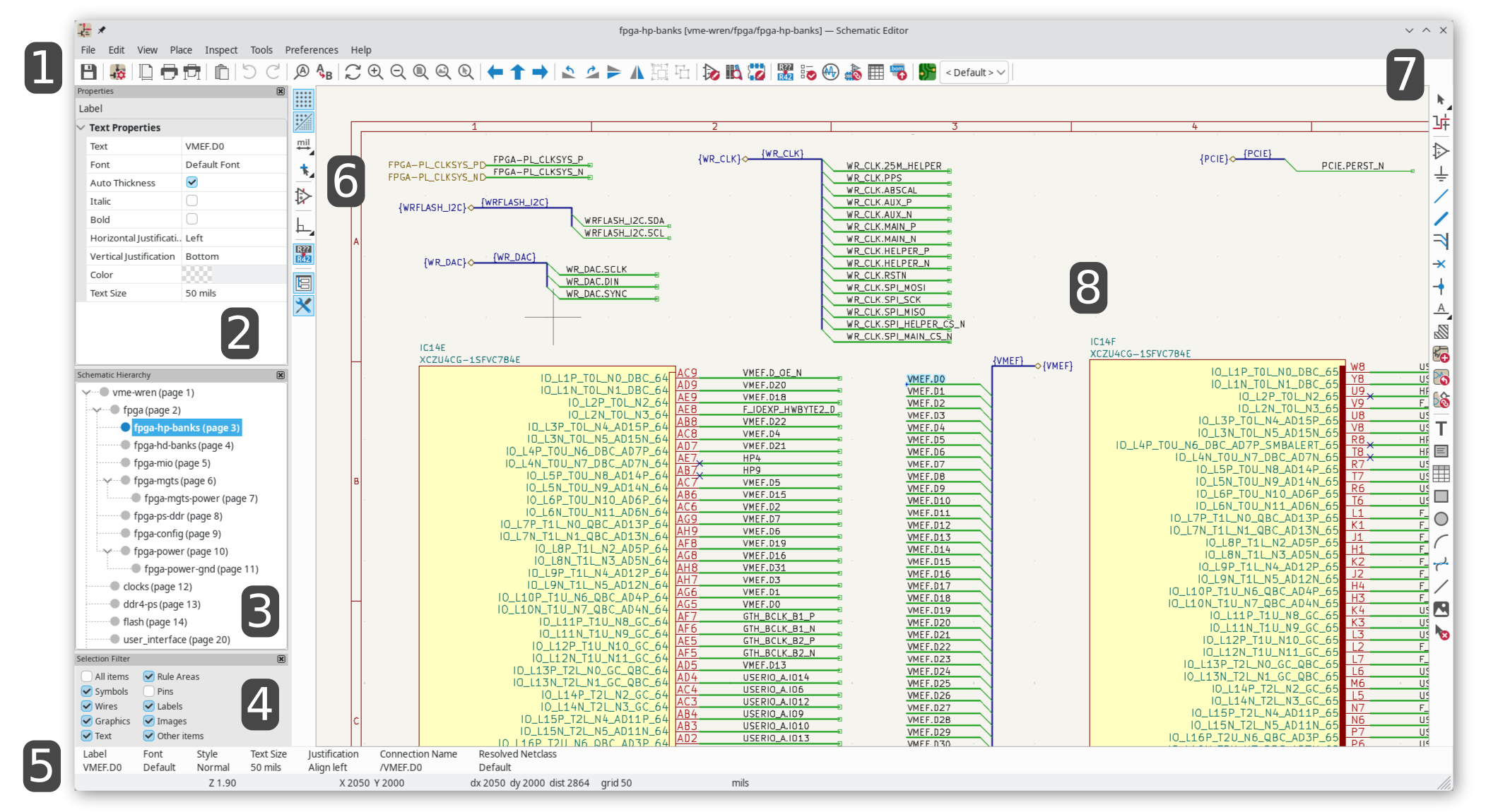
原理图编辑器的用户界面
The main Schematic Editor user interface is shown above, with some key elements indicated:
-
顶部工具栏(文件管理、缩放工具、编辑工具)。
-
Message panel and status bar
-
Editing canvas
浏览编辑画布
编辑画布显示正在设计的原理图。你可以平移和缩放到原理图的不同部分,并打开设计中的任何原理图页。
默认情况下,用鼠标中键或右键拖动会平移画布视图,滚动鼠标滚轮会放大或缩小视图。你可以在偏好设置中的鼠标和触摸板部分改变这一行为(详见配置和定制 )。
在顶部的工具栏中还有其他几个缩放工具:
-
 放大视口中心。
 -
 缩小视口中心。
 -
 放大到适合原理图页大小。
 -
 缩放到适合原理图中的每个对象(不包括图框)。例如,如果有对象放置在图框之外,在放大到对象之后,它们就会显现出来。
 -
 允许你画一个方框来确定缩放的区域。
光标的当前位置显示在窗口的底部(X 和 Y),还有当前的缩放系数(Z)、光标的相对位置(dx、dy 和 dist)、网格设置和显示单位。
按 Space 可以将相对坐标重置为零(dx, dy, and dist)。这对于测量两点之间的距离或对齐物体很有用。
快捷键
按 Ctrl+F1 快捷键显示当前快捷键列表。默认的快捷键列表包括在本手册的 操作参考 部分。
本手册中描述的快捷键使用了标准 PC 键盘上的按键布局。在苹果键盘布局中,使用 Cmd 键来代替 Ctrl,使用 Option 键来代替 Alt。
许多操作默认没有分配快捷键,但可以使用快捷键编辑器(偏好设置 → 偏好设置… → 快捷键)分配或重新定义快捷键。
| 许多通过快捷键进行的操作也可以在上下文菜单中使用。要访问上下文菜单,在编辑画布上点击右键。 根据所选择的内容或所使用的工具,将有不同的操作。 |
快捷键存储在 KiCad 的配置目录下的 user.hotkeys 文件中。这个位置是平台相关的:
-
Windows:
%APPDATA%\kicad\10.0\user.hotkeys -
Linux:
~/.config/kicad/10.0/user.hotkeys -
macOS:
~/Library/Preferences/kicad/10.0/user.hotkeys
KiCad 可以使用快捷键编辑器中的 导入快捷键 按钮从 user.hotkeys 文件中导入快捷键设置。
Selection and the selection filter
Selecting items in the editing canvas is done with the left mouse button. When no tool is active, single-clicking on an object will select it. Pressing Esc will always cancel the current tool or operation and return to the selection tool. Pressing Esc while the selection tool is active will clear the current selection.
You can also select items using a rectangle or lasso selection. These tools can be useful for selecting many items at once. You can switch between rectangular and lasso selection modes using the ![]() /
/ ![]() palette in the right toolbar.
palette in the right toolbar.
| To switch between multiple tools in a palette, show the palette by clicking and holding the left mouse button on the tool icon or by clicking and dragging the mouse from the tool icon. Release the mouse button on the desired tool to choose it. |
With the rectangular selection mode active (![]() ), clicking and dragging will perform a rectangular selection. A rectangular selection from left to right will only select items that are fully inside the box. A rectangular selection from right to left will select any items that touch the box. A left-to-right selection box is drawn in yellow, with a cursor that indicates exclusive selection, and a right-to-left selection box is drawn in blue with a cursor that indicates inclusive selection.
), clicking and dragging will perform a rectangular selection. A rectangular selection from left to right will only select items that are fully inside the box. A rectangular selection from right to left will select any items that touch the box. A left-to-right selection box is drawn in yellow, with a cursor that indicates exclusive selection, and a right-to-left selection box is drawn in blue with a cursor that indicates inclusive selection.
With the lasso selection mode active (![]() ), clicking and dragging will begin a lasso selection. Any items in the existing selection are deselected. Dragging with the left mouse button held draws a freeform shape. Releasing the button stops drawing the freeform shape and starts drawing a straight line. Clicking again completes the straight line. Any number of freeform or straight segments can be drawn by repeatedly clicking or dragging. Double click to finish drawing the lasso. Similar to a rectangular selection, a lasso drawn in a clockwise direction will only select items that are fully inside the lasso. A lasso drawn in a counter-clockwise direction will select any items that touch the lasso. A clockwise lasso is drawn in yellow, with a cursor that indicates exclusive selection, and a counter-clockwise lasso is drawn in blue with a cursor that indicates inclusive selection.
), clicking and dragging will begin a lasso selection. Any items in the existing selection are deselected. Dragging with the left mouse button held draws a freeform shape. Releasing the button stops drawing the freeform shape and starts drawing a straight line. Clicking again completes the straight line. Any number of freeform or straight segments can be drawn by repeatedly clicking or dragging. Double click to finish drawing the lasso. Similar to a rectangular selection, a lasso drawn in a clockwise direction will only select items that are fully inside the lasso. A lasso drawn in a counter-clockwise direction will select any items that touch the lasso. A clockwise lasso is drawn in yellow, with a cursor that indicates exclusive selection, and a counter-clockwise lasso is drawn in blue with a cursor that indicates inclusive selection.
The selection action can be modified by holding modifier keys while clicking or dragging. Modifiers cannot be used with lasso selections.
The following modifier keys apply when clicking to select single items:
| Modifier Keys (Windows) | Modifier Keys (Linux) | Modifier Keys (macOS) | Selection Effect |
|---|---|---|---|
Ctrl |
Ctrl |
Cmd |
Toggle selection. |
Shift |
Shift |
Shift |
Add the item to the existing selection. |
Ctrl+Shift |
Ctrl+Shift |
Cmd+Shift |
Remove the item from the existing selection. |
long click |
long click or Alt |
long click or Option |
Clarify selection from a pop-up menu. |
The following modifier keys apply when dragging to perform a rectangular selection:
| Modifier Keys (Windows) | Modifier Keys (Linux) | Modifier Keys (macOS) | Selection Effect |
|---|---|---|---|
Ctrl |
Ctrl |
Cmd |
Toggle selection. |
Shift |
Shift |
Shift |
Add item(s) to the existing selection. |
Ctrl+Shift |
Ctrl+Shift |
Cmd+Shift |
Remove item(s) from the existing selection. |
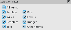
The selection filter panel in the lower left corner of the Schematic Editor window controls which types of objects can be selected with the mouse. Turning off selection of unwanted object types makes it easier to select items in a busy schematic.
The All items checkbox is a shortcut to turn the other items on and off. You can right-click any object type in the selection filter to quickly change the filter to only allow selecting that type of object.
If you repeatedly try to select an object whose type is disabled in the selection filter, the selection filter will visually flash the checkbox for that object type as a reminder that selecting that object type is disabled.
选择一个对象会在窗口底部的信息面板上显示该对象的信息。双击一个对象可以打开一个窗口来编辑该对象的属性。
左侧工具栏显示控制
左侧工具栏提供了改变原理图编辑器中对象显示的选项。
Some toolbar buttons have more than one item available in a palette. These buttons are indicated with a small arrow in the lower-right corner of the button: 
To show the palette, you can click and hold the mouse button on the button or click and drag the mouse. The palette will show the selected item when it is closed.
The default contents of the left toolbar are shown below.
| You can edit the toolbar’s contents in the Toolbar page of the Schematic Editor Preferences. |
|
Turns grid display on/off. Note: by default, hiding the grid does not disable grid snapping. This behavior can be changed in the Display Options section of Preferences. |
|
Turns item-specific grid overrides on/off. |
|
Display/entry of coordinates and dimensions in inches, mils, or millimeters. Clicking the button toggles to the next unit, or you can choose a unit directly by expanding the palette (click and hold/drag). |
|
Switches the cursor crosshair between small, fullscreen, and 45-degree-rotated fullscreen. Clicking the button toggles to the next crosshair type, or you can choose a crosshair directly by expanding the palette (click and hold/drag). |
|
Turns invisible pin display on/off. |
|
Switches the line mode between free angle, 90 degree mode, and 45 degree mode for placement of new wires, buses, and graphical shapes. Clicking the button toggles to the next line mode, or you can choose a line mode directly by expanding the palette (click and hold/drag). You can also toggle between line modes using Shift+Space. |
|
Turns automatic symbol annotation on/off. When on, symbols will have their reference designators automatically set to the lowest available reference when they are added to the schematic. |
|
Opens and closes the docked Hierarchy Navigator panel. |
|
Opens and closes the docked Properties Manager panel. |
原理图创建和编辑
简介
用 KiCad 设计的原理图不仅仅是一个电子设计的简单图形表示。它通常是开发链的切入点,可用于:
原理图主要由符号、导线、标签、结点、总线和电源符号组成。为了使原理图更清晰,你可以放置纯图形元素,如总线入口、注释和折线。
符号是从符号库中添加到原理图中的。原理图制作完成后,网络连接和封装的集合被导入 PCB 编辑器,用于设计电路板。
原理图可以使用单一的原理图页面,也可以分割成多个原理图页面。在 KiCad 中,多张原理图是按层次组织的,有一个根原理图和子原理图。每个原理图都是它自己的 .kicad_sch 文件,它本身就是一个完整的 KiCad 原理图。层次原理图的工作在层次原理图章节中描述。
原理图编辑操作
原理图编辑工具位于右侧工具栏中。 当一个工具被激活时,它将一直处于活动状态,直到选择了另一个工具或用 Esc 键取消该工具。当其他工具被取消时,选择工具总是被激活。
Some toolbar buttons have more than one tool available in a palette. These tools are indicated with a small arrow in the lower-right corner of the button:
To show the palette, you can click and hold the mouse button on the button or click and drag the mouse. The palette will show the most recently selected item when it is closed.
The default contents of the right toolbar are shown below.
| You can edit the toolbar’s contents in the Toolbar page of the Schematic Editor Preferences. |
|
Selection tool (the default tool) When the rectangular selection mode is active, clicking and dragging performs a rectangular selection. When the lasso selection mode is active, clicking and dragging performs a lasso selection. Only one selection mode is visible in the toolbar at a time; you can expand the palette to choose another tool by clicking and holding/dragging. |
|
Highlight a net by marking its wires and net labels with a different color. If the PCB Editor is also open then copper corresponding to the selected net will be highlighted as well. Net highlighting can be cleared by clicking with the highlight tool in an empty space, or by using the Clear Net Highlighting hotkey (~). |
|
Display the symbol selector dialog to place a new symbol. |
|
Display the power symbol selector dialog to place a new power symbol. |
|
|
|
|
|
Draw wire-to-bus entry points. These elements are only graphical and do not create a connection, thus they should not be used to connect wires together. |
|
Place a "no-connection" flag. These flags should be placed on symbol pins which are meant to be left unconnected. "No-connection" flags indicate to the Electrical Rule Checker that the pin is intentionally unconnected and not an error. They also affect schematic connectivity for stacked symbol pins. |
|
Place a junction. This connects two crossing wires or a wire and a pin, which can sometimes be ambiguous without a junction (i.e. if a wire end or a pin is not directly connected to another wire end). |
|
Place a local label, directive label, global label, or hierarchical label. Local labels connect items located in the same sheet. Local labels with the same name are connected as long as they are in the same sheet. Global labels connect items located anywhere in the schematic. All global labels with the same name are connected, even when located on different sheets. Hierarchical labels are used to create a connection between a subsheet and the sheet’s parent sheet. See the Hierarchical Schematics section for more information about hierarchical labels, sheets, and pins. Directive labels are used to assign net classes to individual nets. They can also be used to assign net classes and component classes to nets and symbols, respectively, inside rule areas. Only one label type is visible in the toolbar at a time; you can expand the palette to choose another tool by clicking and holding/dragging. |
|
Place a rule area. |
|
Place a hierarchical subsheet. You must specify the file name for this subsheet. |
|
Place a hierarchical sheet pin on a sheet corresponding to a hierarchical label that has been added in the target sheet. |
|
Sync hierarchical sheet pins and hierarchical labels. This displays a list of all the hierarchical labels in each subsheet and lets you manage the corresponding hierarchical sheet pins. |
|
|
|
|
|
|
|
|
|
|
|
|
|
|
|
Note: Lines are graphical objects and are not the same as wires placed with the Wire tool. They do not connect anything. |
|
|
|
Delete clicked items. |
网格和捕获
Schematic elements such as symbols, wires, text, and graphic lines are snapped to the grid when moving, dragging, and drawing them. Additionally, the wire and label tools snap to other connected items such as pins, wires, and labels even when grid snapping is disabled.
Both grid and connected object snapping can be disabled while moving the mouse by using the modifier keys in the table below.
| 在苹果键盘上,使用 Cmd 键而不是 Ctrl。 |
| Modifier Key | Effect |
|---|---|
Ctrl |
Disable grid snapping. |
Shift |
Disable connected object snapping. |
The default grid size is 50 mil (0.050") or 1.27 millimeters. This is the recommended grid for placing symbols and wires in a schematic and for placing pins when designing a symbol in the Symbol Editor. Smaller grids can also be used, but this is intended only for text and symbol graphics, and not recommended for placing pins and wires.
| 导线只有在两端完全重合的情况下才能与其他导线或引脚连接。因此,保持符号引脚和导线与网格对齐是非常重要的。建议在放置符号和绘制导线时始终使用 50 mil 的网格,因为 KiCad 标准符号库和所有遵循其风格的库也使用 50 mil 的网格。使用 50 mil 以外的网格尺寸将导致原理图没有正确的连接!。 |
| 符号、导线和其他没有对准网格的元素,可以通过选择它们,点击右键,并点击 将元素对准网格,将它们重新对准网格。 |
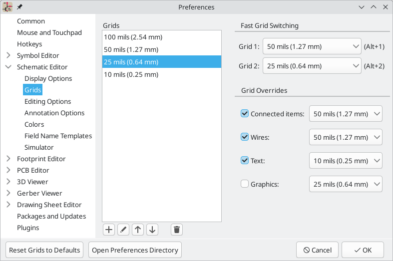
You can adjust the grid size by right-clicking and selecting a new grid from the list in the Grid submenu. Pressing the n or N hotkeys will cycle to the next and previous grid in the list, respectively.
You can also select a new grid or edit the available grids in the Grids pane of the preferences dialog. As a shortcut to reach this dialog, right click the ![]() button on the left toolbar and select Edit Grids….
button on the left toolbar and select Edit Grids….
In this dialog you can select an active grid from the list of grids, reorder the list of grids (![]() /
/ ![]() ), and add (
), and add (![]() ), remove (
), remove (![]() ), or edit (
), or edit (![]() ) grids. Grids defined in this dialog can have unequal X and Y spacing as well as an optional name. The grid spacing and name are specified when you create or edit a grid.
) grids. Grids defined in this dialog can have unequal X and Y spacing as well as an optional name. The grid spacing and name are specified when you create or edit a grid.
This dialog also lets you designate two grids from the list as "Fast Grids", which can be quickly selected using Alt+1 and Alt+2.
Finally, you can configure grid overrides for different types of objects. Grid overrides let you set particular grid sizes for different types of objects which will be used instead of the default grid when working with those objects. For example, you can set a 50 mil grid for wires and connected items while using smaller grids to finely position text and graphics. Grid overrides can be individually enabled and disabled in this dialog, or globally enabled and disabled using the ![]() button on the left toolbar (Ctrl+Shift+G).
button on the left toolbar (Ctrl+Shift+G).
The visual appearance of the grid can also be customized in several ways. You can change the thickness of the grid markings, switch their shape (dots, lines, or crosses), and set the minimum displayed spacing in the Display Options page of the preferences dialog, and you can change the grid color in the Colors page of the preferences dialog.
The grid can be shown or hidden using the ![]() button on the left-hand toolbar. By default the grid is still active even if it is hidden, but this is configurable in the Display Options preferences page. There you can set the grid to be disabled when it is hidden or even disable the grid entirely.
button on the left-hand toolbar. By default the grid is still active even if it is hidden, but this is configurable in the Display Options preferences page. There you can set the grid to be disabled when it is hidden or even disable the grid entirely.
编辑对象属性
All objects have properties that are editable in a dialog. Use the hotkey E or select Properties from the right-click context menu to edit the properties of selected item(s). You can only open the properties dialog if all the items you have selected are of the same type. For many object types, like symbols, you can only edit the properties of a single item at one time. To edit the properties of multiple items at once, including items with different types, you can use the Properties Manager.
You can only use the properties dialog to edit one item at a time. To edit multiple items, use the Properties Manager, described below. There are also other tools that can be used to edit specific types of objects in bulk, such as the Edit Text and Graphics tool for editing visual properties of text, symbol fields, labels, and graphic shapes, or the Symbol Fields Table for editing symbol fields in bulk.
You can also view and edit item properties using the Properties Manager. The Properties Manager is a docked panel that displays the properties of the selected item or items for editing. If multiple types of items are selected at once, the properties panel displays only the properties shared by all of the selected item types.
Editing a property in the Properties Manager immediately applies the change. When multiple items are selected, property modifications are applied to each selected item individually, not to the whole selection as a group. For example, when changing the orientation of multiple items, each item is individually rotated around its own origin, not the group’s origin.
Show the Properties Manager with View → Panels → Properties or the ![]() button on the left toolbar.
button on the left toolbar.
In properties dialogs and many other dialogs, any field that contains a numeric value can also accept a basic math expression that results in a numeric value.
For example, a dimension may be entered as 2 * 2mm, resulting in a value of 4mm. Basic arithmetic operators as well as parentheses for defining order of operations are supported. Units can also be specified, and unit conversions are performed automatically, so 1in + 1mm evaluates to 26.4mm.
使用符号
放置符号
要将符号摆放到原理图中,可以使用图标 ![]() 或者快捷键 A 。 出现选择符号对话框,让您选择要添加的符号。 符号按符号库分组。
或者快捷键 A 。 出现选择符号对话框,让您选择要添加的符号。 符号按符号库分组。
默认情况下,仅显示符号/库名称和描述列。 可以通过右键单击列标题并选择“选择列”来添加其他列。
The Choose Symbol dialog filters symbols by name, keywords, description, and all additional symbol fields according to what you type into the search field. You can choose to sort search results alphabetically or by best match by clicking on the ![]() button.
button.
有一些高级筛选器可用:
-
Wildcards:
*matches any number of any characters, including none, and?matches any single character. -
Key-value pairs: if a library part’s description or keywords contain a tag of the format "Key:123", you can match relative to that by typing "Key>123" (greater than), "Key<123" (less than), etc. Numbers may include one of the following case-insensitive suffixes:
p
n
u
m
k
meg
g
t
10-12
10-9
10-6
10-3
103
106
109
1012
ki
mi
gi
ti
210
220
230
240
-
Regular expressions: if you’re familiar with regular expressions, these can be used too. The regular expression flavor used is the wxWidgets Advanced Regular Expression style, which is similar to Perl regular expressions.
如果符号指定了一个默认的封装,这个封装将在右下方预览。如果符号包括封装过滤器,可以在右边的封装下拉菜单中选择满足封装过滤器的备用封装。
选择一个要放置的符号后,该符号将被吸附在光标上。 左键点击原理图中所需要摆放的位置,将符号放入原理图中。在将符号放入原理图之前,可以通过快捷键或右键菜单来旋转、镜像或编辑它的字段。这些操作也可以在放置后进行。
如果 放置重复副本 选项被选中,在放置一个符号后 KiCad 将开始放置该符号的另一个副本。这个过程一直持续到用户按下 Esc。
对于有多个单元的符号,如果 放置所有单元 选项被选中,在放置符号后 KiCad 将开始放置该符号中的下一个单元。 这将持续到最后一个单元被放置或用户按下 Esc。
放置电源符号
电源符号是代表与电源网络连接的符号。 这些符号被分组在 power 库中,所以可以使用符号选择器来放置。 然而,由于电源的放置很频繁,![]() 工具是可用的。这个工具使用方法类似,只是搜索是直接在
工具是可用的。这个工具使用方法类似,只是搜索是直接在 power 库和其他包含电源符号的库中进行。
移动符号
符号可以用移动(M)或拖动(G)工具移动。这些工具将作用于选定的符号,如果没有选定符号,则作用于光标下的符号。
移动 工具移动符号本身,而不保持与符号引脚的导线连接。
拖动 工具在移动符号时不会破坏其引脚的导线连接,因此也会移动连接的导线。
你也可以用鼠标点击并拖动符号,这取决于偏好设置中 鼠标和触摸板 部分的 左键拖动手势 设置。
符号也可以旋转(R)或在X(X)或Y(Y)方向上进行镜像。
编辑符号属性
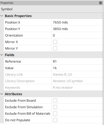
Symbols in the schematic can be individually edited, both in terms of their properties (fields, attributes, etc.) and in terms of their pins and graphics. Editing a symbol in the schematic only affects that particular instance of the symbol; it does not affect any other copies of that symbol in the schematic, and it does not affect the library symbol.
To edit the properties of a symbol in the schematic, open its properties dialog (E). You can also double-click the symbol.
The majority of the settings in this dialog are the same as in the symbol editor. You can edit the symbol’s fields, attributes, pin functions, and embedded files, as in the symbol editor.
The Symbol Properties window displays all the fields of a symbol in a table. New fields can be added, and existing fields can be deleted, edited, reordered, moved, or resized. Fields can be arbitrarily named, but names beginning with ki_, e.g. ki_description, are reserved by KiCad and should not be used for user fields. All symbol fields will be added to the symbol’s corresponding footprint when the PCB is updated from the schematic.
每个字段的名称和值可以是可见的或隐藏的,并且有几个格式化选项:水平和垂直对齐、方向、位置、字体、文本颜色、文本大小和黑体/斜体。字段的自动放置也可以在每个字段的基础上启用。显示位置始终针对正常显示的符号(无旋转或镜像)指示,并且与符号的锚点相关。
| 符号字段的格式化选项可以通过右击符号字段表的标题行来显示或隐藏,并启用或禁用所需的列。默认情况下,不是所有的列都显示。 |
Several fields have special behavior:
-
The Footprint field defines which footprint will correspond to the symbol in the board design. When the footprint field is selected, you can click the
 button to open the footprint chooser to assign a footprint to the symbol. See the Assigning Footprints section for other ways to assign footprints.
 -
The Datasheet field can contain the manufacturer’s datasheet for the symbol. You can right click a symbol in the editing canvas and choose Show Datasheet (D) to open the datasheet listed in the symbol. A symbol’s datasheet can be a local file or a file at a remote URL, like the manufacturer’s website. You can choose a local file using a file browser by selecting the datasheet field in the symbol’s properties, then clicking the
 button. If you enable the Embed File checkbox in the file browser, the datasheet will be embedded in the schematic instead of being referenced as an an external file. This means the datasheet will be available on any computer. For more information, see the embedded files documentation.
符号有几个属性,它们会影响 KiCad 其他部分对符号的处理方式。
-
Exclude from simulation prevents the symbol from being included in SPICE simulations. Symbols that are excluded from simulation are drawn with a grey outline around them and a simulation waveform icon to their bottom right, as shown below. The color of the outline and icon is configurable by editing the "Excluded-from-simulation Markers" color in the selected colorscheme. The visual marker (the outline and the icon) can be disabled completely by disabling View → Mark items which are excluded from simulation.

-
Exclude from bill of materials prevents the component from being included in BOM exports.
-
Exclude from board means that the symbol is schematic-only, and a corresponding footprint will not be added to the PCB.
-
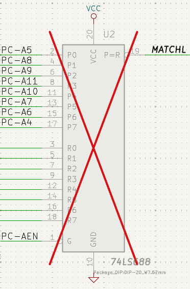
Do not populate means that the component should not be attached to the PCB, although a corresponding footprint should still be added to the board. DNP symbols appear desaturated and with a red "X" over them in the schematic, as shown below. The color of the "X" is configurable by editing the "DNP Markers" color in the selected colorscheme.
To edit the symbols’s form, i.e. its pins and graphics, you need to use the symbol editor. There are two buttons for opening a symbol in the editor, depending on whether you want to edit a single copy of a symbol in the schematic or a symbol’s source copy in the library.
-
Edit Symbol… will open the specific instance of the symbol in the symbol editor. Editing this symbol will only affect this one instance of the symbol in the schematic. It will not affect other instances of the symbol in the schematic, and it will not affect the library copy of the symbol. You can also open a schematic symbol in the symbol editor by right clicking the symbol in the schematic and selecting Edit with symbol editor (Ctrl+E).
-
Edit Library Symbol… will open the library copy of the symbol in the symbol editor. Editing the library copy of the symbol will edit the symbol in the symbol library, but will not immediately affect any instances of that symbol in the schematic. To update symbols in the schematic with changes to the library symbol, use the Update Symbol from Library… tool. Editing the library symbol in this way is equivalent to opening the symbol editor, opening the appropriate symbol in its library, and editing it.
The Update Symbol from Library… button is used to update the schematic’s copy of the symbol to match the copy in the library. The Change Symbol… button is used to swap the current symbol to a different symbol in the library. These functions are described later.
The Simulation Model… button opens the Simulation Model Editor for specifying the symbol’s behavior in SPICE simulations.
单独编辑符号字段
可以用 E 快捷键直接编辑单个符号文本字段(选择字段而不是符号),或者双击字段。
一些符号字段有自己的快捷键,可以直接编辑它们。选定符号后,可分别用 U、V 或 F 快捷键编辑位号、值和封装字段。
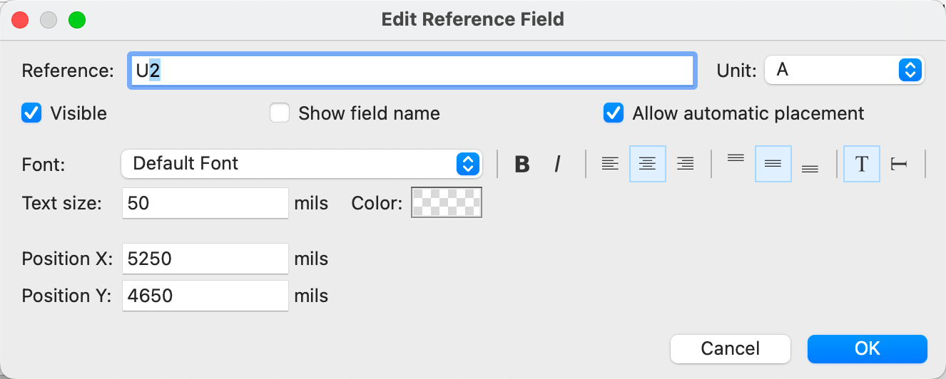
该对话框中的选项与完整的 "符号属性" 对话框中的选项相同,但都是针对单个字段的。
Symbol fields can be automatically moved to an appropriate location with the Autoplace Fields action (select a symbol and press O). Field autoplacement is configurable in the Schematic Editor’s Editing Options, including a setting to always autoplace fields. You can also disable autoplacement for individual fields in the Symbol Properties or Field Properties dialogs.
Alternate pin functions
Symbol pins can have alternate pin functions defined for them. Alternate pin functions allow you to select a different name, electrical type, and graphical style for a pin when a symbol has been placed in the schematic. This can be used for pins that have multiple functions, such as microcontroller pins.
Alternate pin functions are selected once a symbol has been placed in the schematic. The pin function is selected in the Pin Functions tab of the Symbol Properties dialog. Alternate definitions are selectable in the dropdown in the Alternate Assignment column. You can also select an alternate pin by right-clicking the pin and selecting a new function from the Pin Function menu.
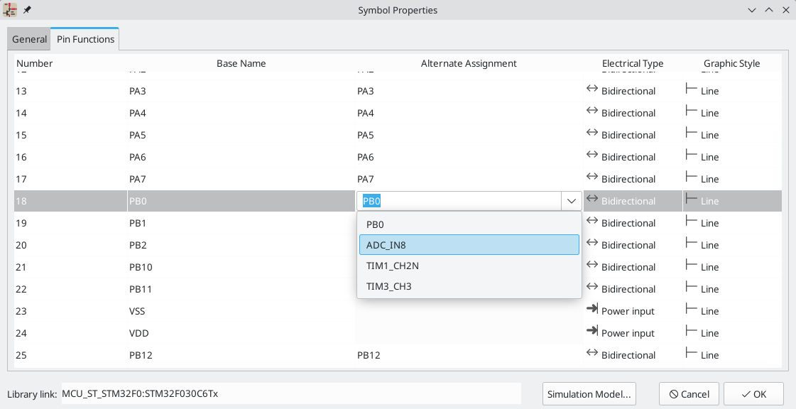
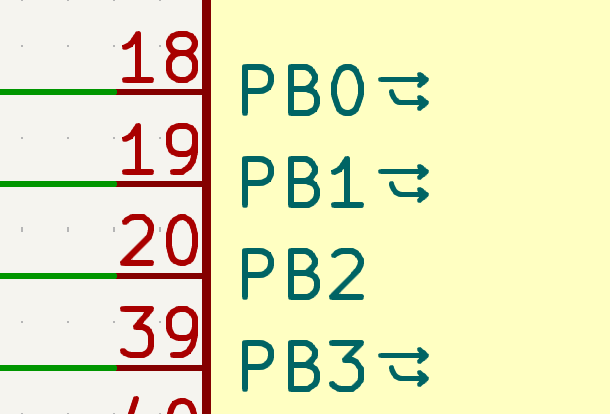
Pins that have alternate functions available are displayed with a small graphical indicator next to the pin name, as shown in the screenshot below. To globally show or hide these indicators, use View → Show Pin Alternate Icons.
For information on how to add alternate pin functions to symbols, see the symbol editor documentation.
Updating and exchanging symbols
When a symbol is added to the schematic, KiCad embeds a copy of the library symbol in the schematic so that the schematic is independent of the system libraries. Symbols that have been added to the schematic are not automatically updated when the library changes. Library symbol changes are manually synced to the schematic so that the schematic does not change unexpectedly.
| You can use the Compare Symbol with Library tool to inspect the differences between a symbol in a schematic with its corresponding library symbol. |
To update symbols in the schematic to match the corresponding library symbol, use Tools → Update Symbols from Library…, or right click a symbol and select Update Symbol…. You can also access the tool from the symbol properties dialog.
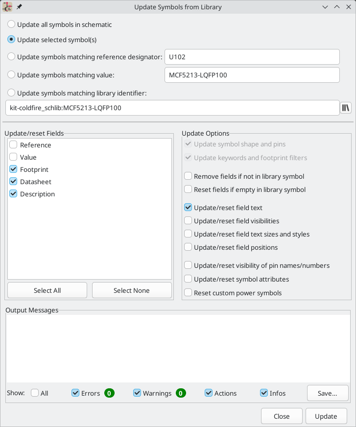
The top of the dialog has options to choose which symbols will be updated:
-
Update all symbols in schematic: all symbols in the schematic will be updated to match the library versions of the symbols.
-
Update selected symbol(s): symbols that are selected in the schematic will be updated.
-
Update symbols matching reference designator: symbols matching the specified reference designator will be updated. The reference designator field supports wildcards:
*matches any number of any characters, including none, and?matches any single character. -
Update symbols matching value: symbols with the specified value will be updated. The value field supports wildcards:
*matches any number of any characters, including none, and?matches any single character. -
Update symbols matching library identifier: symbols that match the specified library identifier will be updated. Library identifiers consist of the symbol library name and the symbol name, separated by
:.
The middle of the dialog has options to control what parts of the symbol will be updated. On the left, you can select which fields will be modified (updated or reset). On the right, you can select how to update those fields:
-
Remove fields if not in library symbol: if selected, any fields that are in the schematic version of the symbol but not the library version will be deleted.
-
Reset fields if empty in library symbol: if selected, any fields that are empty in the library version of the symbol will be set to empty in the schematic version of the symbol.
-
Update/reset field text: if selected, field contents in the schematic version of the symbol will be updated to match the fields in the library version of the symbol. Any fields that are empty in the library version of the symbol will not be updated unless Reset fields if empty in library symbol is selected.
-
Update/reset field visibilities: if selected, fields in the schematic version of the symbol will have their visibility updated to match the library version of the symbol.
-
Update/reset field text sizes and styles: if selected, fields in the schematic version of the symbol will have their text sizes and styles updated to match the library version of the symbol.
-
Update/reset field positions: if selected, fields in the schematic version of the symbol will be moved to match the locations of the fields in the library version of the symbol.
-
Update symbol shape and pins: the symbol’s shape and pins are always updated to match the library version of the symbol.
-
Update keywords and footprint filters: The symbol’s keywords and footprint filters are always updated to match the library version of the symbol.
-
Update/reset pin name/number visibilities: if selected, the visibility of pin names and numbers in the schematic version of the symbol will be updated to match the visibility of the pin names and numbers in the library version of the symbol.
-
Reset alternate pin functions: if selected, alternate pin functions selected for the symbol’s pins will be reset to default pin functions.
-
Update/reset symbol attributes: if selected, the schematic symbol attributes (do not populate, exclude from simulation, exclude from BOM, exclude from board) will be updated to match the library version of the symbol.
-
Reset custom power symbols: if selected, the
Valuefield of power symbols in the schematic will be updated to match the library versions of the symbols. If not selected, theValuefield of power symbols will not be updated, even if theValuefield of other non-power symbols would be updated. Note that changing theValuefield of power symbols will change the global net associated with the power symbol.
The bottom of the dialog displays messages describing the update actions that have been performed, with filters for which types of messages to display (errors, warnings, actions, and/or infos).
To change an existing symbol to a different symbol, use Edit → Change Symbols…, or right click an existing symbol and select Change Symbol…. This dialog is also accessible from the symbol properties dialog.
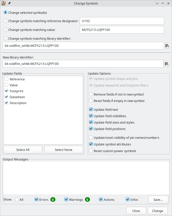
The options for the Change Symbols dialog are very similar to the Update Symbols from Library dialog.
Another way to swap existing symbols for new ones is to use Tools → Edit Symbol Library Links…. This dialog contains a table of every symbol in the design, grouped by current library symbol. By choosing a new symbol in the New Library Reference column, you can make all instances of the existing symbol instead point to the new symbol. If the Update symbol fields from new library option is used, the contents of the existing symbols' fields will be updated to match the new symbols' fields.
The Map Orphans button attempts to automatically remap orphaned symbols to symbols with the same name in an active library. For example, if there is a symbol with the current library reference mylib:symbol123, but the mylib library cannot be found, the Map Orphans button will attempt to find a symbol named symbol123 in any of the libraries that are present. This button is only enabled if orphaned symbols are present in the schematic (see the legacy schematics section).
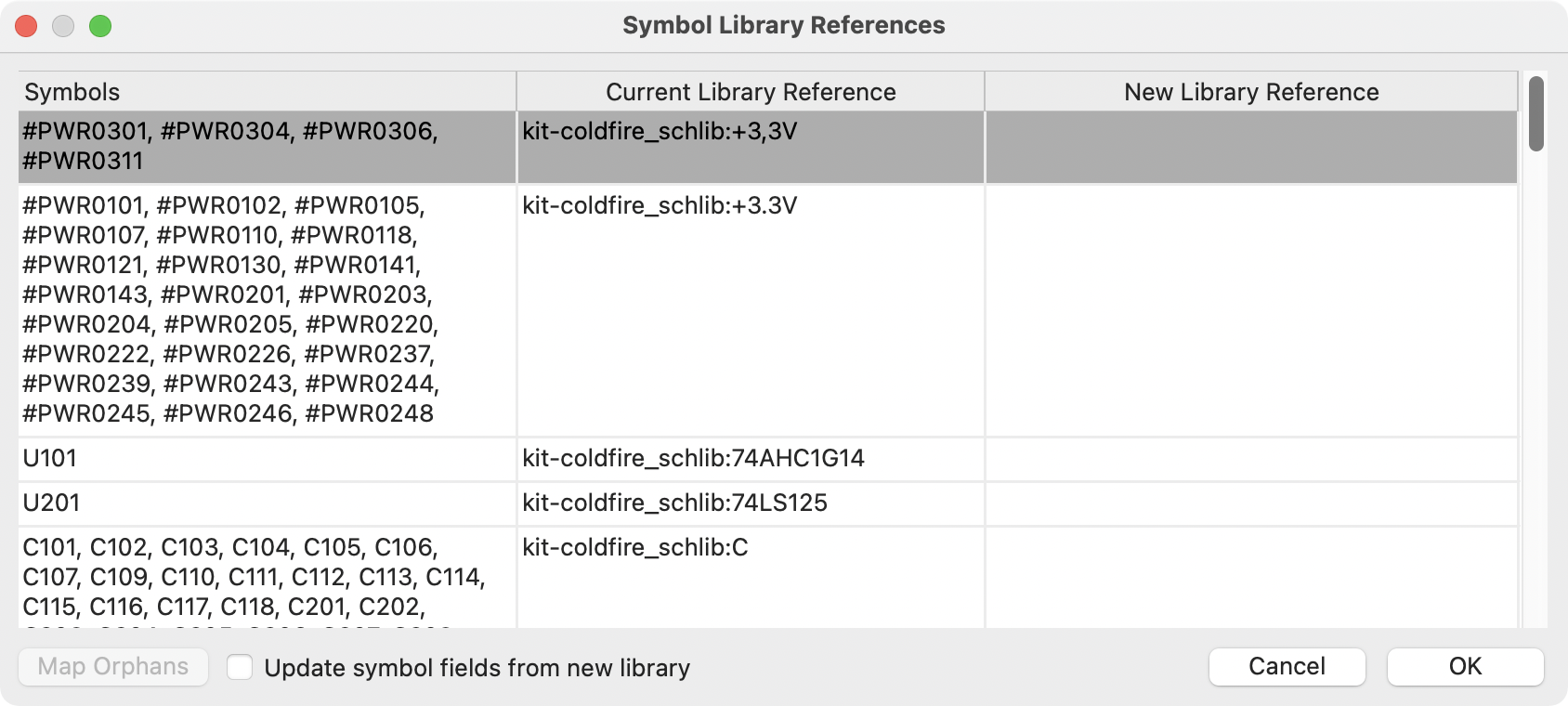
This dialog is primarily useful for managing symbols that appear in multiple libraries, when you want to switch from one library to another. For example, if a schematic uses symbols that are in both a global library and a project-specific library, the Symbol Library References dialog could be used to switch between using the global symbols or the equivalent project-specific symbols. It does not have features for fine-grained control of how fields are updated; for that, use the Change Symbols dialog.
Comparing symbols between schematic and library
When a symbol in a schematic diverges from the corresponding symbol in the original symbol library, you can use the Compare Symbol with Library tool to inspect the differences between the two versions of the symbol. Run the tool using Inspect → Compare Symbol With Library.
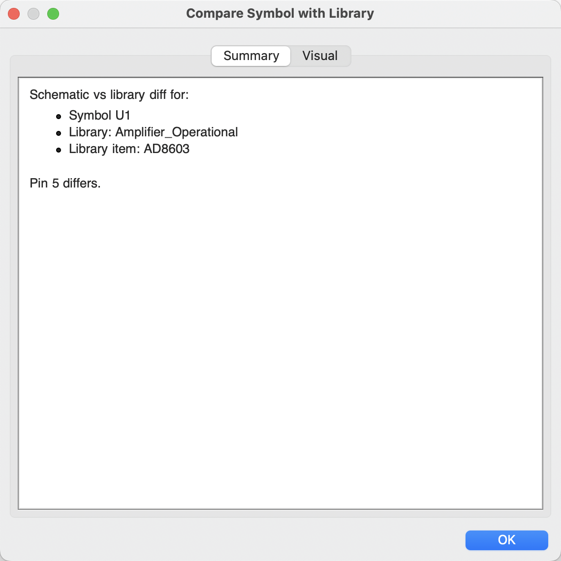
The Summary tab shows the name of the symbol, including its library and schematic reference designator, and provides a list of the differences between the schematic and library versions of the symbol.
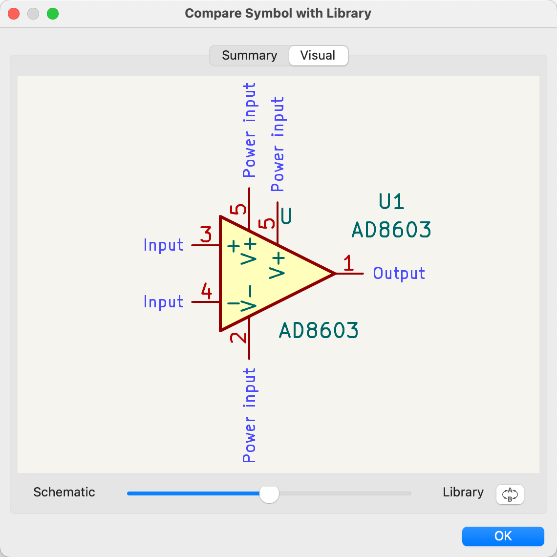
The Visual tab shows a visual comparison of the schematic and library versions of the symbol. This can be used as a visual diff tool.
By default, the comparison displays both versions of the symbol superimposed on each other. To see the changes more easily, you can drag the slider at the bottom of the tab to the right to emphasize the library version of the symbol in the superimposed view (making the schematic version of the symbol more transparent) or drag it to the left to emphasize the schematic version (making the library version more transparent). At the far right and left ends of the slider, the schematic and library versions of the symbol, respectively, are fully hidden. It may be helpful to drag the slider back and forth to see the changes more clearly.
You can press the A/B button, or use the / hotkey, to quickly toggle back and forth between the schematic and library versions.
The Update Symbol from Library… button opens the Update Symbol from Library tool to update the symbol to match the library.
The screenshot above shows a visual comparison with the schematic version of the symbol deemphasized. You can see a partially transparent pin 5 (from the schematic version of the symbol) is in a different location than the fully opaque pin 5 (from the library symbol). This indicates that the pin was moved in either the schematic or library version of the symbol.
符号字段表
The Symbol Fields Table allows you to view and modify field values for all symbols in a spreadsheet interface. The Symbol Fields Table also acts as a BOM export tool. You can open the Symbol Fields Table with the ![]() button.
button.
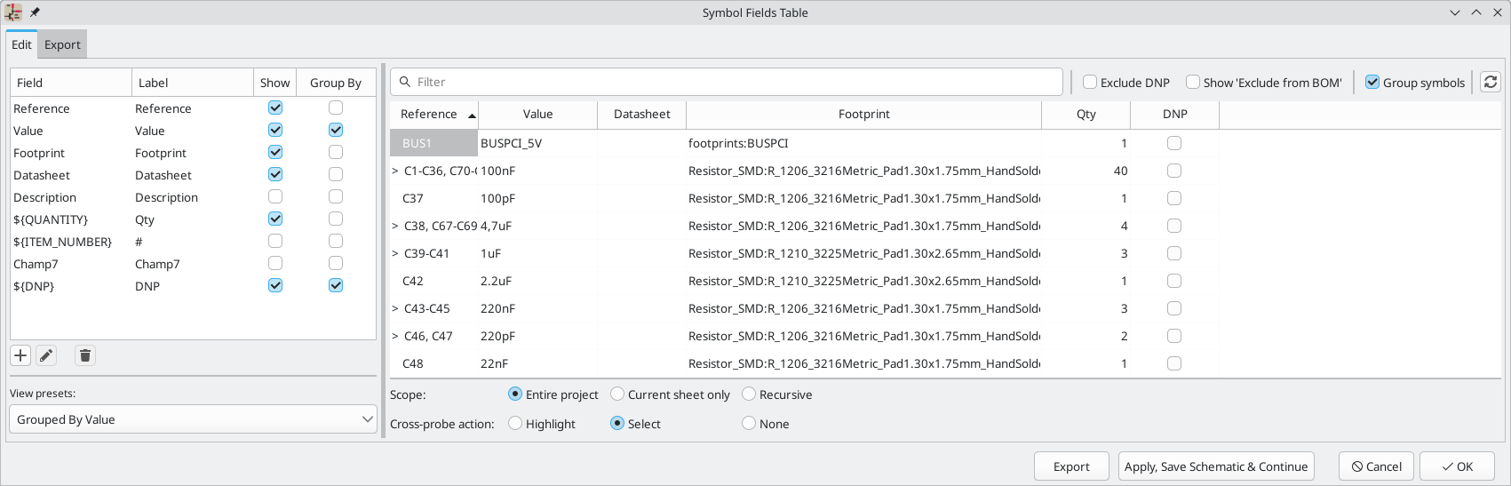
The main table has a row for each symbol and a column for each field. Each cell is editable.
Symbol fields that contain text variables, such as a field set to ${VALUE},
are displayed in the table as their resolved value.
Clicking on the cell to edit it shows the unresolved text variable.
Such cells are shown with a yellow background to indicate the field contains a text variable.
|
Cells are navigated with the arrow keys, or with Tab / Shift+Tab to move right / left and Enter to move down, respectively.
通过点击和拖动可以选择一个单元格范围。选定的整个单元格范围可以通过(Ctrl+C)或(Ctrl+V)进行复制或粘贴。从表中复制单元格的对于创建 BOM 非常有用。下面将介绍复制和粘贴单元格的更多细节。
The left pane contains a list of all available symbol fields, as well as some virtual fields such as Quantity and Item Number. You can add or remove any symbol field from the main table on using the Include checkboxes (fields can also be shown or hidden by right-clicking on the header of the main table). New symbol fields can be added using the ![]() button; a field with that name will be added to every symbol. To rename the field, which changes the field name in all symbols, use the
button; a field with that name will be added to every symbol. To rename the field, which changes the field name in all symbols, use the ![]() button. The
button. The ![]() button deletes the field from all symbols. You can collapse this panel by clicking the
button deletes the field from all symbols. You can collapse this panel by clicking the ![]() button.
button.
Each field has its own column label, which is displayed at the top of the corresponding column in the symbol fields table and in exported BOMs. The column label for each field is shown in the second column of in the left pane. A column label does not have to match the field name. To change a field’s column label, click in the BOM Name column for that field, then enter a new name.
Similar symbols can optionally be grouped by any symbol field using the Group By checkboxes. Symbols are grouped into a single row in the table if all of their Group By fields are identical. The grouped row can be expanded to show the individual symbols by clicking the arrow at the left of the row. The Group symbols checkbox enables or disables symbol grouping, and the ![]() button recalculates groupings.
button recalculates groupings.
预置可用于配置字段列表。预置可存储显示的字段、用于分组的字段以及列顺序。 您可以创建并保存自己的预置,也可以使用多个默认预置之一。 自定义预置可以在此对话框或 《原理图设置,原理图设置》 对话框中删除。
Symbols can be filtered by reference designator using the Filter textbox at the top. The filter supports wildcards: * matches any number of any characters, including none, and ? matches any single character.
You can also change the display scope using the dropdown menu to the right of the filter box. You can show only symbols in the current sheet, the current sheet and all of its subsheets, or the entire project.
The ![]() menu contains some additional options for showing or hiding symbols.
menu contains some additional options for showing or hiding symbols.
-
Include 'DNP' Symbols includes or excludes symbols with the Do Not Populate attribute from both the Edit tab and any BOM exports.
-
Include 'Exclude from BOM' Symbols includes or excludes symbols with the Exclude from BOM attribute from the Edit tab. Symbols with the Exclude from BOM attribute are always excluded from BOM exports.
You can cross-probe from this dialog by selecting a row in the table. Depending on the cross-probe options selected in the ![]() menu, this can highlight the corresponding symbol in the schematic, select the corresponding symbol in the schematic, or do nothing. The selection action can also select the symbol’s footprint in the board editor, depending on the PCB Editor cross-probing settings configured in Preferences.
menu, this can highlight the corresponding symbol in the schematic, select the corresponding symbol in the schematic, or do nothing. The selection action can also select the symbol’s footprint in the board editor, depending on the PCB Editor cross-probing settings configured in Preferences.
The Symbol Fields Table is also a bill of materials tool. You can use the Export button to save the symbol fields to an external file. The fields are exported to the BOM exactly as they are currently shown in the spreadsheet view. File format settings are configured in the Export tab. For more information about exporting a BOM, see the BOM tool documentation.
Virtual fields
If you create a field in the Symbol Fields Table whose name begins with a text variable, a virtual field will be created. Virtual fields have a value that is evaluated for each symbol based on the contents of the field name. For example, a virtual field named ${SYMBOL_NAME} will evaluate to the symbol’s name for each symbol. A virtual field can contain any text, as long as it starts with a text variable, so a virtual field named ${SYMBOL_LIBRARY}:${SYMBOL_NAME} will evaluate to <library name>:<symbol name> for each symbol.
Virtual fields exist only in the Symbol Fields Table and in BOM exports. While they are displayed as a column in the dialog and BOMs, and they can be used to group or sort symbols in BOM exports just like regular fields, adding a virtual field in the Symbol Fields Table does not add a corresponding field to each symbol in the schematic.
Any text variable can be used in virtual fields, including sheet and project text variables.
Text variables that correspond to symbol attributes (${DNP}, ${EXCLUDE_FROM_BOARD}, ${EXCLUDE_FROM_SIM}, ${EXCLUDE_FROM_BOM}) are displayed specially. In the Symbol Fields Table, they are shown as checkboxes for each symbol that directly set or unset the corresponding symbol attribute. In BOM exports, they expand to the friendly name of the attribute if the attribute is set (e.g. Excluded from board for ${EXCLUDE_FROM_BOARD} and DNP for ${DNP}) or to an empty string if the attribute is not set.
Finally, there are two special virtual fields that can be created:
-
${QUANTITY}is a virtual field that contains the number of grouped instances of each symbol. -
${ITEM_NUMBER}is a virtual field that contains the row number of each symbol in the table.
简化填写字段的技巧
电子表格中有几种特殊的复制/粘贴方法,用于将数值粘贴到更大的区域,包括自动增加粘贴的单元格。这些功能在粘贴几个符号中共享的数值时可能很有用。
这些方法如下所示。
| 1. Copy (Ctrl+C) | 2. Select target cells | 3. Paste (Ctrl+V) |
|---|---|---|
|
|
|
|
|
|
|
|
|
|
|
|
|
|
|
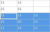
| 这些技巧在其他带有网格控制元素的对话框中也可以使用。 |
Reference designators and symbol annotation
位号是设计中元件的唯一标识符。它们通常被印在 PCB 和装配图上,使你能够将原理图中的符号与电路板上的相应元件相匹配。
在 KiCad 中,位号由一个表示元件类型的字母(R 表示电阻,C 表示电容,U 表示集成电路,等等)及后面的数字组成。如果符号有多个单元,那么位号也会有一个表示单位的尾部字母。没有设置位号的符号有一个 ? 字符,而不是数字。位号必须是唯一的。
位号可以在符号添加到原理图时自动设置,也可以通过手动编辑单个符号的位号字段或使用批注工具批量设置或重置位号。
| 设置一个符号的位号的过程被称为 批注。 |
自动批注
When auto-annotation is enabled, symbols will be automatically annotated when they are added to the schematic. You can enable auto-annotation by checking the Automatically annotate symbols checkbox in the Schematic Editor → Editing Options pane in Preferences. Auto-annotation can also be toggled using the ![]() button in the left toolbar.
button in the left toolbar.
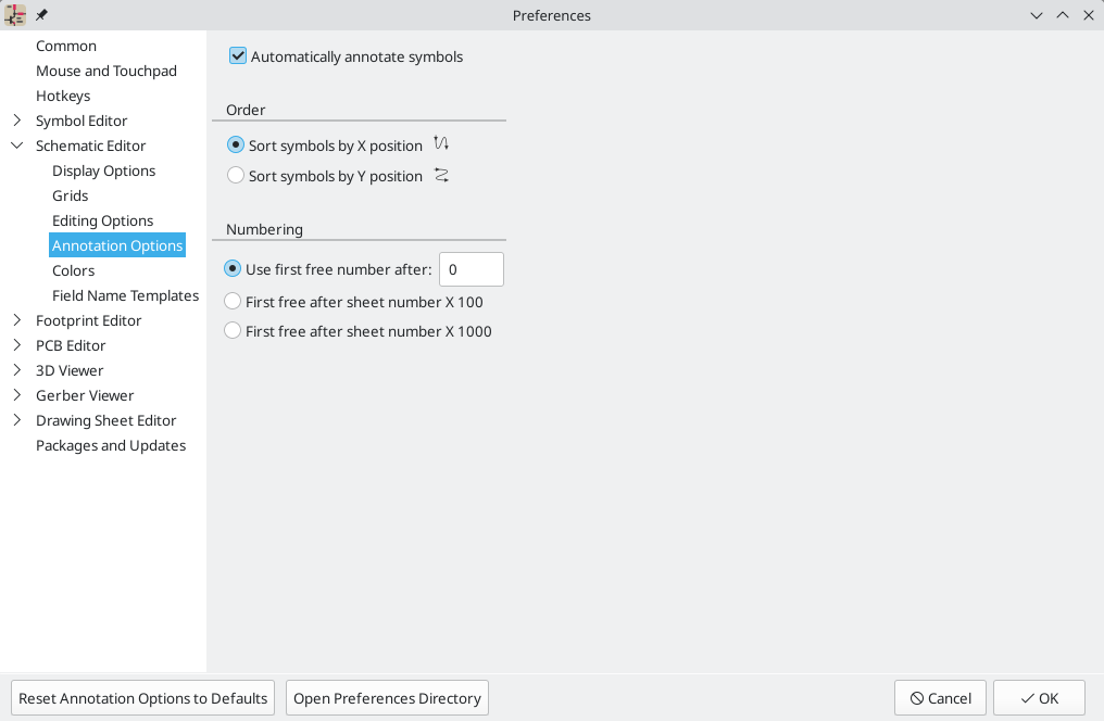
There are options to control how symbols are automatically annotated in the Annotation page of Schematic Setup.
-
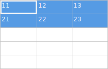
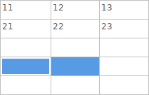
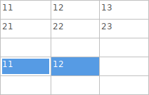
当同时添加多个符号时,它们会根据 顺序 设置进行批注,按 X 或 Y 位置排序。
-
The Numbering option sets the starting number for new reference designators. This can be the lowest available number, or a number based on the sheet number. When Allow reference reuse is enabled, reference designators can be automatically assigned as long as they are not currently used by another symbol. When disabled, a reference designator can never be used again once it has been assigned to a symbol, even if it is not currently in use.
For more information about annotation options, see the documentation for the Annotation page of Schematic Setup.
批注工具
The Annotation tool assigns reference designators to symbols in the schematic. To launch the Annotation tool, click the ![]() button in the top toolbar.
button in the top toolbar.
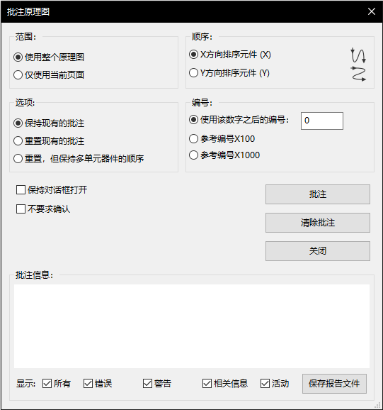
该工具提供了几个选项来控制符号的批注方式。
Scope: Selects whether annotation is applied to the entire schematic, to only the current sheet, or to only the selected symbols. If the Recurse into subsheets option is selected, symbols in subsheets of the selected scope will be reannotated; otherwise symbols in subsheets will not be reannotated. For example, if Recurse into subsheets and Selection only selected, symbols in any selected subsheets will be reannotated.
Options: Selects whether annotation should apply to all symbols and reset existing reference designators, or apply only to unannotated symbols. If the Reset symbol units option is enabled, symbol units will be reannotated individually. This means symbol units may be grouped into symbols differently after reannotation. When it is disabled, each symbol’s units will be reannotated as a group so that they remain together as units of the same symbol.
Order: Chooses the direction of numbering. If symbols are sorted by X position, all symbols on the left side of a schematic sheet will be lower numbered than symbols on the right side of the sheet. If symbols are sorted by Y position, all symbols on the top of a sheet will be lower numbered than symbols at the bottom of the sheet.
Numbering: Selects the starting point for numbering reference designators. The lowest unused number above the starting point is picked for each reference designator. The starting point can be an arbitrary number (typically zero), or it can be the sheet number multiplied by 100 or 1000 so that each part’s reference designator corresponds to the schematic page it is on.
清除批注 按钮可以清除所选范围内的所有位号。
批注信息可以用底部的复选框进行过滤,或用 保存… 按钮保存到报告中。
Electrical connections
Electrical connections in KiCad are known as nets, where each net represents a circuit node. All symbol pins on the same net are considered electrically connected.
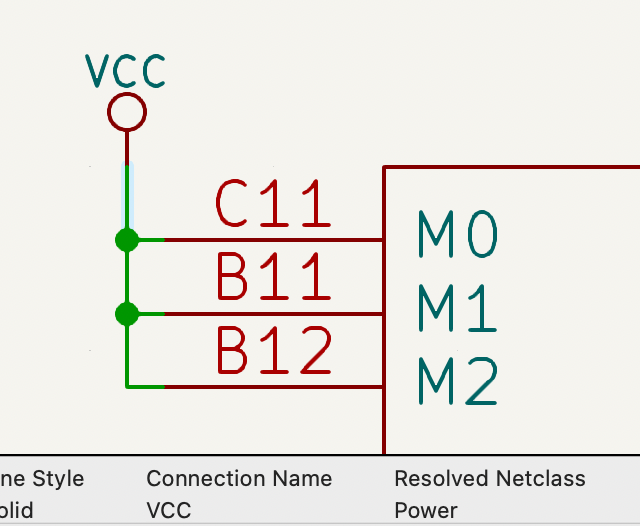
There are two primary ways to establish connections: wires and labels. Wires make direct connections between symbol pins and other wires, while labels connect to other labels with the same name. Both wires and labels are shown in the schematic below.
Connections can also be made with buses and with implicit connections via hidden power pins.
网络名分配规则
Every net in the schematic is assigned a name, whether that name is specified by the user (using a label) or automatically generated by KiCad.
当多个标签附加到同一个网时,最终的网络名将按以下顺序确定,从最高优先级到最低:
-
-
Output sheet pins are higher priority than Input sheet pins
-
如果一个网络有多个同一类型的标签,则按字母顺序排序,使用第一个。
如果一个网络经过层次的多张原理图,它的名字将取决于层次结构中优先级最高的标签。通常,局部标签优先级高于层次标签。
如果以上标签类型都没有添加到网络中,那么网络的名称将根据连接的符号引脚自动生成。
导线
导线用于在两点之间直接建立电气连接。 要建立连接,必须将一段导线的末端与另一段导线或一个引脚相连。只有导线的末端才能建立连接;如果一根导线穿过另一根导线的中间,不会建立连接。
未连接的导线端有一个小方块,表示连接点。 当连接到导线端时,这个方块就会消失。未连接的引脚有一个圆圈,连接完成时时也会消失。
| 导线只有在两端完全重合的情况下才能与其他导线或引脚连接。因此,保持符号引脚和导线与网格对齐很重要。建议在放置符号和绘制导线时始终使用 50 mil 的网格,因为 KiCad 标准符号库和所有遵循其风格的库也使用 50 mil 的网格。 |
| 符号、导线和其他没有对准网格的元素,可以通过选择它们,右键点击,并选择 将元素对准网格,来将它们重新对准网格。 |
绘制和编辑导线
用导线连接对象,请使用右侧工具栏中的导线工具 ![]() (w)。也可以通过点击未连接的符号引脚或导线末端进行导线连接。
(w)。也可以通过点击未连接的符号引脚或导线末端进行导线连接。
可以用左侧工具栏的 ![]() 按钮将导线限制在 90 度角,或者用
按钮将导线限制在 90 度角,或者用 ![]() 按钮将导线限制在 45 度角。
按钮将导线限制在 45 度角。![]() 按钮允许你以任何角度放置导线。可以使用 Shift+Space 在这些模式中循环,或者在 偏好设置 → 原理图编辑器 → 编辑选项 中选择所需的模式。这些模式除了影响导线外,还影响 图形线。
按钮允许你以任何角度放置导线。可以使用 Shift+Space 在这些模式中循环,或者在 偏好设置 → 原理图编辑器 → 编辑选项 中选择所需的模式。这些模式除了影响导线外,还影响 图形线。
与 PCB编辑器中一样, 快捷键 / 切换导线的模式。
可以使用移动(M)或拖动(G)工具来移动和编辑导线。 与符号一样,移动 工具只移动选定的线段,而不保持与其他导线的现有连接。而 拖动 工具则保持现有的连接。
You can select connected wires using the Select Connection tool (Ctrl+4). This tool selects all connected wire segments until it reaches a junction, starting with the selected segment or the segment under the cursor. Using the tool again expands the existing selection to the next junction.
你可以通过右击导线并选择 分割 将一个导线分成两段。该导线将在当前的鼠标位置被分开。你也可以通过右击一个导线并选择 断开 将其与相邻的导线分开。
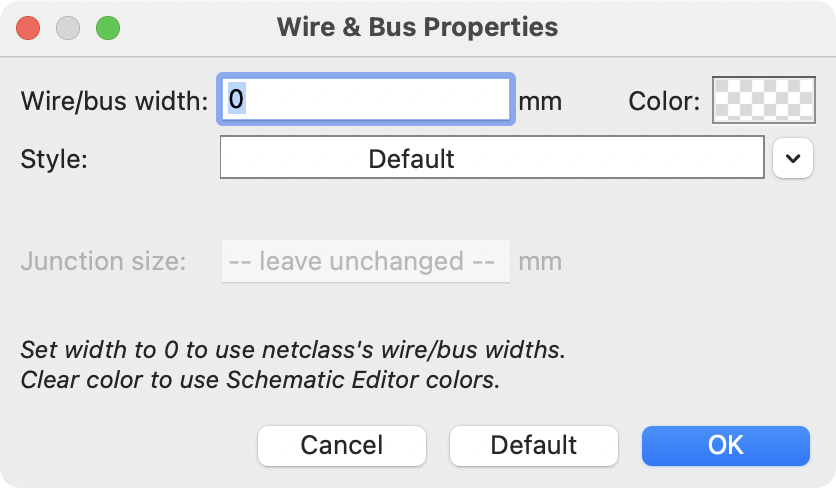
Normally the line style of a wire follows the net’s net class settings (nets are in the Default net class if no other net class is specified). However, the line style for the selected wire segments can be overridden in the wire’s properties dialog (E when a wire segment is selected). The wire’s width, color, and line style (solid, dashed, dotted, etc.) can be set. Setting the width to 0, clearing the color, and using the Default line style uses the default width, color, and style, respectively, from the net class settings. If a wire junction is included in the selection, the junction size can also be edited here.
Wire junctions
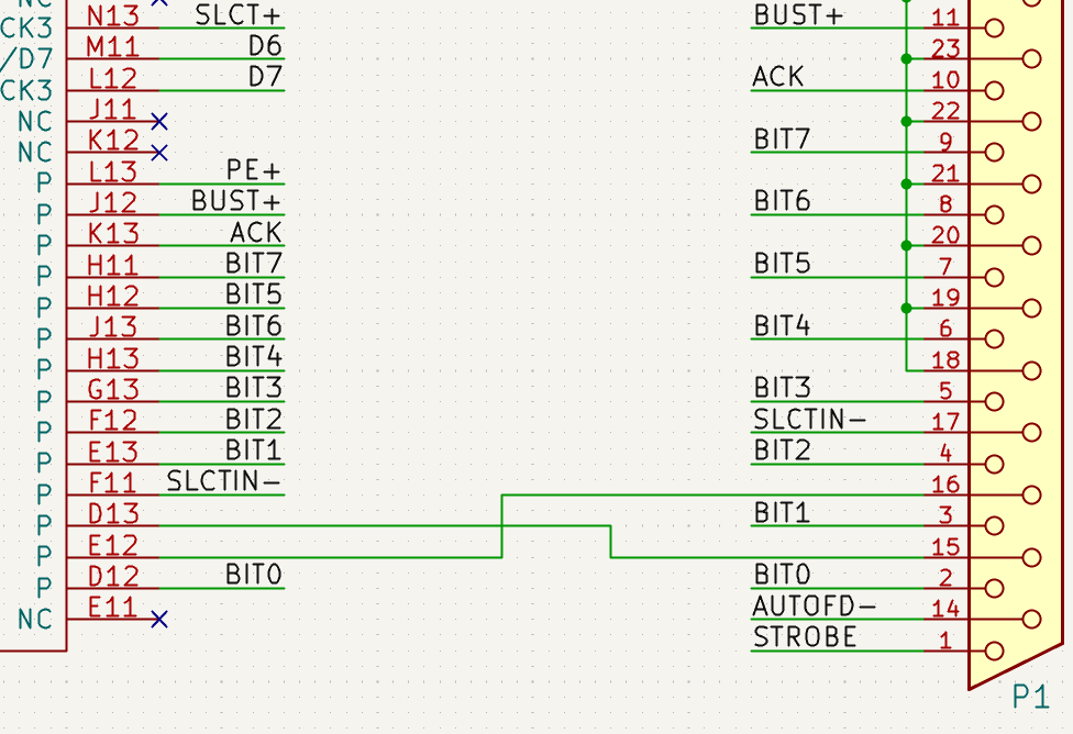
交叉的导线不是隐式连接的。如果需要连接,必须明确地添加结点来连接它们(![]() 按钮在右侧工具栏)。结点将被自动添加到开始或结束于现有导线之上的导线。
按钮在右侧工具栏)。结点将被自动添加到开始或结束于现有导线之上的导线。
在上面的原理图中,连接到 P1 引脚 18、19、20、21、22 和 23 的导线上使用了结点。
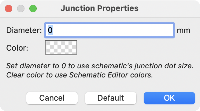
Junction size automatically follows the schematic’s Junction dot size setting in Schematic Setup → General → Formatting. Color follows the net class setting. The automatic size and color can be overridden in each junction dot’s properties; a size of 0 is equivalent to the schematic default size, and clearing the color uses the net class color.
Wire hop-overs
When wires cross without a junction dot, they do not connect. By default, this is drawn simply as one wire crossing through the other wire. However, you can configure such crossovers to be visually indicated with hop-overs instead of simple intersections, as shown in the schematic below. The size of hop-overs is configurable for a given schematic; all hop-overs in the schematic have the same size.
To enable display of hop-overs, open the Formatting page of Schematic Setup and change the Hop-over size setting from None to another size.
标签
标签是用来给导线和引脚分配网络名称的。具有相同网络名称的导线被认为是连接在一起的,所以标签可以用来进行连接,而不需要直接画线连接。
A net can only have one name. If two different labels are placed on the same net, an ERC violation will be generated. Only one of the net names will be used in the netlist. The final net name is determined according to the rules described below.
有三种类型的标签,每种都有不同的连接范围。
-
Local labels, also referred to simply as labels, only make connections within a sheet. Add a local label with the
 button in the right
toolbar.
button in the right
toolbar. -
Global labels make connections anywhere in a schematic, regardless of sheet. Add a global label with the
 button in the right
toolbar.
button in the right
toolbar. -
Hierarchical labels connect to hierarchical sheet pins and are used in hierarchical schematics for connecting child sheets to their parent sheet. Add a hierarchical label with the
 button in the right toolbar.
| 如果在同一个原理图页面,无论标签类型如何,具有相同名称的标签将被连接。 |
| You can convert from one type of label to another type of label using the Change To tools. |
添加和编辑标签
使用相应按钮或快捷键创建标签后,会出现标签属性对话框。
The Label field sets the label’s name, which determines the net that the label assigns to its attached wire or pin. You can choose a label name from a list of nets that are already in the schematic by clicking the dropdown menu next to the label name field.
| Net names can contain any character, including spaces and other special characters. |
Label text supports markup for overbars, subscripts, etc., as well as variable substitution. Use the Syntax help link in the dialog for a summary.
When the Multiple label input option is enabled, the Label field supports entering multiple labels, with one label on each line. In this case, the dialog will create multiple independent labels in sequence, one per line.
| Multiple label input may be useful for copying labels from other sources, such as a spreadsheet. |
有几个选项可以控制标签的外观。你可以改变文本的 字体、大小和颜色,并设置粗体和斜体以便强调。 你还可以设置文本相对于标签连接点的方向。层次和全局标签有几个额外的选项:自动 选项根据连接的原理图元素自动设置标签方向,形状 选项控制标签轮廓的形状(输入、输出、双向、三态 或 被动)。轮廓形状纯粹是视觉上的,没有电气上的影响。
| 在原理图设置对话框 中,全局标签有额外的设置来控制标签文本周围的边距。 |
标签也可以添加字段。有两个字段有特殊的意义("网络类" 和 "页面位号",下面会介绍),但也可以添加任意字段。标签字段的行为类似于符号字段:你可以显示或隐藏它们的名称和值,调整对齐方式、方向、位置、大小、字体、颜色或进行强调。
| 通过右击标签字段表的标题行,可以显示或隐藏标签字段的格式化选项,并启用或禁用所需的列。默认情况下,并非所有的列都显示。 |
与符号字段一样,标签字段可以通过从原理图中打开特定标签字段的属性进行单独编辑(双击标签字段,或使用 E)。
After accepting the label properties, the label is attached to the cursor for placement. The connection point for a label is the small square in the corner of the label. The square disappears when the label is connected to a wire or the end of a pin. If multiple labels were specified in the dialog, each label is attached to the cursor for placement after the previous label is placed.

连接点相对于标签文本的位置可以通过在标签的属性中选择不同的标签方向,或通过镜像/旋转标签来改变。
通过选择一个标签并使用 E 快捷键、双击该标签或在右键菜单中使用 属性…,可以随时访问标签属性对话框。
用标签分配网络类
In addition to assigning net names, labels can be used to assign net classes. A label field named Net Class assigns the specified net class to the net associated with the label. To make it easier to assign net classes in this way, Net Class is the default name for new label fields, and Net Class fields present a dropdown list of all the net classes that have been specified in Schematic Setup or Board Setup.
You can also type in a net class that isn’t explicitly listed in the Schematic/Board Setup priority list. Such implicit net classes can’t be assigned any design settings, like net class color or track width, but they can still be used in DRC rule queries.
If multiple Net Class fields are added to a label, or multiple labels with Net Class fields are applied to a net, all of the specified net classes are assigned to the net.
For more information about assigning net classes, see the net class documentation.
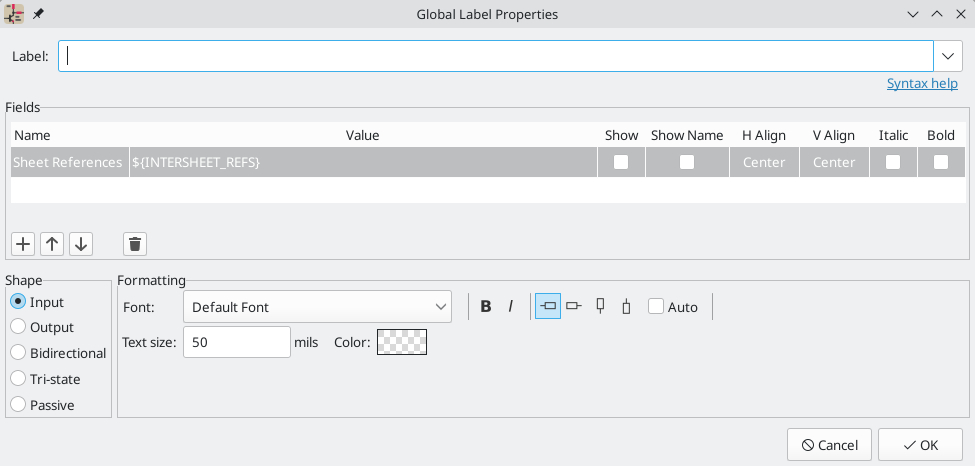
页面间引用
全局标签可以显示页面间引用,它展示了原理图中出现同一全局标签的其他地方的页码列表。 点击页面间引用就可以进入所列出的页面。如果列出了多个引用,点击引用列表会弹出一个菜单来选择所需的页面。
页面间引用在 原理图设置 窗口的格式页面中进行全局控制。 可以启用或禁用引用,并且可以调整列表的显示格式,包括可选的前缀或后缀字符。
下图显示了一个全局标签,其中有对其他两个原理图页面的引用。在原理图设置中,分别添加了前缀和后缀 [ 和 ] 。
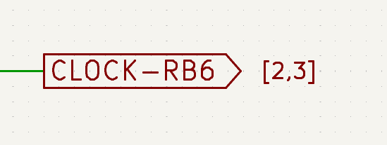
全局标签会自动添加一个 "页面参考" 字段,其值为 "${INTERSHEET_REFS}",用于控制该标签的页面间引用。${INTERSHEET_REFS} 文本变量会被扩展为全局标签页面间引用的完整列表,和在原理图设置中的一致。页面间引用的可见性在 "原理图设置" 中全局控制,而不是通过 "页面间引用" 字段的可见性控制。对于其他类型的标签,"页面间引用" 字段没有意义。
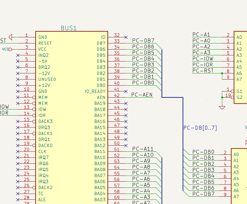
总线
总线是一种在原理图中分组相关信号的方法,以简化复杂的设计。 总线可以像导线一样用总线工具画出来 ![]() ,并像信号线一样用标签命名。
,并像信号线一样用标签命名。
在下面的原理图中,许多引脚都连接到总线上,也就是中间的蓝色粗线。
总线成员
在 KiCad 6.0 及以后版本中,有两种类型的总线:矢量总线和分组总线。
一个 矢量总线 是一个信号的集合,以一个共同的前缀开始,以一个数字结束。 矢量总线被命名为 <前缀>[M..N],其中`前缀`是任何有效的信号名称,M 是第一个后缀数字,N 是最后的后缀数字。 例如,总线 DATA[0…7] 包含信号 DATA0、DATA1,以此类推,直到 DATA7。 指定 M 和 N 的顺序并不重要,但两者必须是非负数。
Vector bus prefixes cannot contain the characters {, }, [, or ], except as part of markup for superscripts, subscripts, overbars, or text variables. Prefixes may contain spaces, but the spaces must be escaped. You can escape spaces in the prefix either by preceding the space with a backslash (\) or by surrounding the entire prefix with double quotes ("). For example, DATA\ BUS[0..7] and "DATA BUS"[0..7] are both valid vector bus names.
一个 分组总线 是一个或多个信号和/或矢量总线的集合。 分组总线可以用来把相关的信号捆绑在一起,即使它们有不同的名字。 分组总线使用一种特殊的标签语法:
‘<OPTIONAL_NAME>{SIGNAL1 SIGNAL2 SIGNAL3}’
该分组的成员被列在大括号({})内,用空格字符隔开。 在大括号的前面有一个可选的分组名。 如果分组总线没有命名,PCB 中产生的网络将作为该分组内的信号名称。 如果分组总线有名字,产生的网络将以名字为前缀,用句号(.)分隔前缀和信号名称。
例如,总线 {SCL SDA} 有两个信号成员,在网表中这些信号将是 SCL 和 SDA。 总线 USB1{DP DM} 将产生名为 USB1.DP 和 USB1.DM 的网表。 对于在几个类似电路中重复出现的较大的总线的设计,使用这种技术可以节省时间。
分组总线也可以包含矢量总线。 例如,总线 MEMORY{A[7..0] D[7..0] OE WE} 同时包含了矢量总线和普通信号,并将在 PCB 上形成 MEMORY.A7 和 MEMORY.OE 这样的网络。
Group bus names cannot contain the characters {, }, [, or ], except as part of markup for superscripts, subscripts, overbars, or text variables. Group bus names and the constituent net names may contain spaces, but the spaces must be escaped. You can escape spaces either by preceding the space with a backslash (\) or by surrounding the entire group bus name or net name with double quotes ("). For example, DATA\ BUS{SIGNAL\ 1 SIGNAL\ 2}, "DATA BUS"{"SIGNAL 1" "SIGNAL 2"}, and "DATA BUS"{SIGNAL\ 1 "SIGNAL 2"} are all valid (and equivalent) labels for group buses.
总线的绘制和连接方式与信号线相同,包括使用结点来创建交叉线之间的连接。 与信号线一样,总线不能有一个以上的名称—如果在同一总线上有两个冲突的标签,将产生一个 ERC 违规。
总线成员之间的连接
总线相同成员之间连接的引脚必须通过标签连接。不可能将一个引脚直接连接到总线上;这种连接方式将被 KiCad 忽略。
在上面的例子中,连接是通过放置在连接到引脚的导线上的标签来实现的。连接总线的总线入口(45 度的线段)只是图形化的,并不是形成逻辑连接的必要条件。
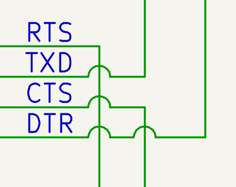
事实上,使用重复命令(Insert),如果元件引脚以递增的顺序排列,可以非常快速地进行连接(在实践中,这种情况常见于存储器、微处理器等元件):
-
放置第一个标签(例如:
PCA0)。 -
尽量使用重复命令来放置成员。 KiCad 将自动创建下一个标签(
PCA1,PCA2…)垂直对齐,理论上是在其他引脚的位置上。 -
在第一个标签下画线。然后使用重复命令将其他导线放在标签下。
-
如果需要,以同样的方式放置总线入口(放置第一个入口,然后使用重复命令)。
|
在偏好设置菜单的 原理图编辑器 → 编辑选项 部分,你可以设置重复的参数:
|
总线展开
展开工具允许你快速地从总线上分离出信号。 要展开一个信号,请右击一个总线对象(一个总线导线等),并选择 从总线上展开。 或者,当光标在一个总线对象上时,使用 展开总线 快捷键(默认:C)。 该菜单允许你选择要展开的总线成员。
在选择总线成员后,下一次点击将把总线成员的标签放在所需的位置。 该工具会自动生成一个总线入口和通向标签位置的导线。 放置完标签后,你可以继续放置额外的导线(例如,连接到一个元件引脚),并以任何正常方式完成布线。
总线别名
总线别名是一种快捷方式,可以让你更有效地处理大型分组总线。 它允许你定义一个分组总线,并给它一个简短的名称,然后可以在整个原理图中代替完整的分组名称。
要创建总线别名,请在原理图设置中打开 总线别名定义 窗格。
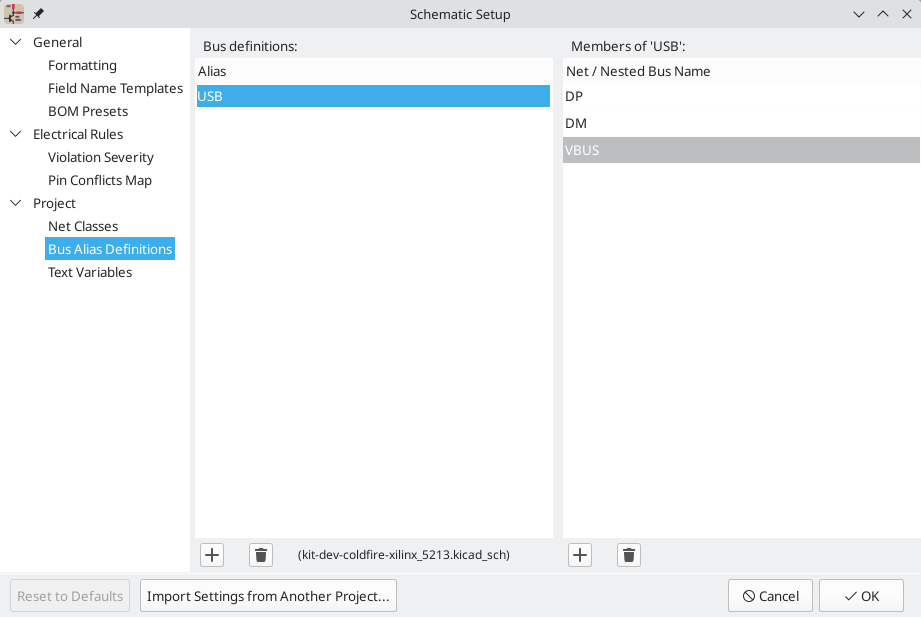
一个别名可以被命名为任何有效的信号名称。 使用该对话框,你可以向别名添加信号或矢量总线。 作为一种快捷方式,你可以输入或粘贴信号和/或总线的列表,用空格隔开,它们将全部被添加到别名定义中。 在这个例子中,我们定义了一个名为 USB 的别名,成员为 DP、DM 和 VBUS。
After defining an alias, it can be used in a group bus label by putting the alias name inside the curly braces of the group bus: {USB}. This has the same effect as labeling the bus {DP DM VBUS}: the nets will be DP, DM, and VBUS. You can also add a prefix name to the group, such as USB1{USB}, which results in nets such as USB1.DP. For complicated buses, using aliases can make the labels on your schematic much shorter. Keep in mind that the aliases are just a shortcut, and the name of the alias is not included in the netlist.
总线别名被保存在创建别名时打开的原理图文件中。在 总线别名定义 窗口中,与所选别名相关的原理图文件显示在别名列表的底部。在一个给定的原理图页面中创建的任何别名都可以在同一层次设计中的任何其他原理图页面中使用。如果一个层次设计中的多个原理图包含相同名称的总线别名,这些别名必须都有相同的成员。如果多个同名的总线别名没有一致的成员,ERC 将报告违规情况。
Bus example
In the schematic below, a bus alias named USB is defined with members DP, DN.
The root sheet has three buses, one with label {USB}, with no prefix, and two with prefixes: USB1{USB} and USB2{USB}. The first bus results in nets DP and DN, the second results in nets USB1.DP and USB1.DN, and the third results in nets USB2.DP and USB2.DN.
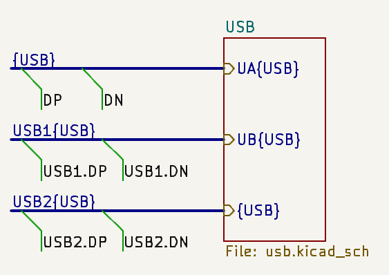
When connecting to a sub-sheet, the hierarchical labels (and therefore hierarchical sheet pins) are named with the same syntax. They need the same members as the connected bus. As for bus labels, hierarchical labels can define a prefix or not. In this case, the hierarchical labels are named {USB} (i.e. no prefix) and UA{USB} and UB{USB}.
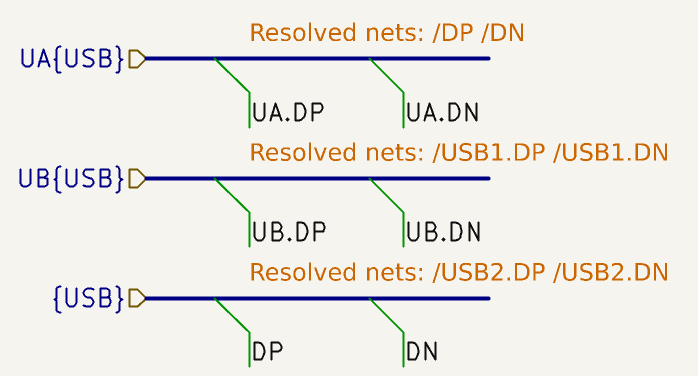
Within the subsheet, the hierarchical labels for the bus are what define the prefixes of displayed labels of unfolded bus members on that sheet. However, the nets resolve according to the connectivity with the parent sheet.
For example, the bus member labeled UB.DP in the subsheet has the label prefix UB due to the hierarchical label, and the resolved net name /USB1.DP due to the name of the bus in the parent sheet that connects to that hierarchical label.
有多个标签的总线
KiCad 5.0 或更早的版本允许将具有不同标签的总线连接在一起,并在网表编制时将这些总线的成员连接起来。这种行为在 KiCad 6.0 中被移除了,因为它与分组总线不兼容,而且还会导致网表的混乱,因为一个给定的信号将得到的名称不容易预测。
如果您在现代版本的 KiCad 中打开使用此功能的设计,您将看到“迁移总线”对话框,该对话框将指导您更新原理图,以便在任何给定的总线线路上只存在一个标签。
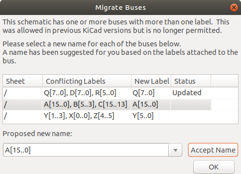
对于具有多个标签的每组总线,您必须选择要保留的标签。 下拉名称框允许您在设计中存在的标签之间进行选择,或者您可以选择一个不同的名称并手动将新名称输入名称字段。
Power symbols
Power symbols are symbols that are conventionally used to represent a connection to a power net, such as VCC or GND. Power symbols are virtual: they do not represent a physical component on the PCB.
In addition to being a visual indicator that the attached net is a power rail, power symbols make global connections: two power symbols with the Value connect to each other anywhere in the schematic, regardless of sheet. The power symbol’s Value field determines the name of the attached net.
| In previous versions of KiCad, power symbols used invisible power input pins, which make implicit global connections based on the pin name as described below. Beginning in KiCad 8, power symbols do not need to use invisible pins, and the global connection is made based on the power symbol’s value. |
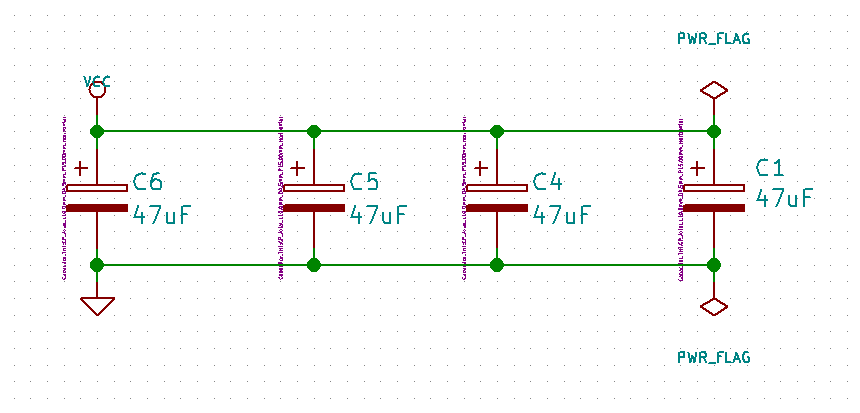
在下图中,电源符号用于将电容器的正负极分别连接到 VCC 和 GND 网络上。
In the KiCad standard library, power symbols are found in the power library, but power symbols can be created in any library. Creating custom power symbols is described in the symbol editor documentation. Instead of making a new symbol, you can also modify an existing power symbol in the schematic: changing its Value field will change the net the power symbol connects to.
PWR_FLAG
上面的截图中可以看到两个 PWR_FLAG 符号。它们向 ERC 表明,两个电源网络 VCC 和 GND 实际上连接到一个电源上,虽然没有明确的电源输出(如电压调节器输出)连接到以上两个网络。
如果没有这两个标志,ERC 工具会诊断出:错误:输入电源引脚没有被任何输出电源引脚驱动。
PWR_FLAG 符号可以在 power 符号库中找到。将任何电源输出引脚连接到网络上,可以达到同样的效果。
Hidden power pins
When the power pins of a symbol are visible, they must be connected, as with any other signal. However, symbols are sometimes drawn with hidden power input pins, which are connected implicitly. KiCad automatically connects invisible pins with type Power Input to a global net with the same name as the pin. For example, if a symbol has a hidden power input pin named VCC, this pin will be globally connected to the VCC net on all sheets. This kind of implicit connection is not recommended in new designs.
| Care must be taken with hidden power input pins because they can create unintentional connections. By nature, hidden pins are invisible and do not display their pin name. This makes it easy to accidentally connect two power pins to the same net. For this reason, using invisible power pins in symbols is not recommended and is only supported for compatibility with legacy designs and symbols. |
|
隐藏的引脚可以在原理图中显示,方法是在 原理图编辑器 → 偏好设置的 显示选项 部分勾选 显示隐藏的引脚,或者选择 视图 → 显示隐藏的引脚。在左侧工具栏上还有一个切换是否显示隐藏引脚的图标 |
No-connection flags
No-connection flags (![]() ) are used to indicate that a pin is intentionally unconnected. These flags prevent "unconnected pin" ERC warnings for pins that are intentionally unconnected. Also, while symbol pins that are stacked on top of each other are normally connected to the same net, if a no-connection flag is added to the stacked pins they will instead be connected to separate nets.
) are used to indicate that a pin is intentionally unconnected. These flags prevent "unconnected pin" ERC warnings for pins that are intentionally unconnected. Also, while symbol pins that are stacked on top of each other are normally connected to the same net, if a no-connection flag is added to the stacked pins they will instead be connected to separate nets.
Note that no-connection flags are distinct from the "unconnected" symbol pin type, although they both prevent "unconnected pin" ERC warnings on the pin in question and prevent stacked pins from connecting to each other.
网络类
Net classes are named groupings of nets that can be assigned design rules (for the PCB) and graphical properties (for the schematic).
More than one net class can be assigned to a net (through a combination of graphical assignments and net class patterns). For nets with multiple net classes assigned, an effective aggregate net class is formed, taking any net class properties from the highest priority net class which has that property set. Net class priority is determined by the ordering in the Schematic or Board Setup dialogs. The Default net class is used as a fallback for any missing properties after all explicit net classes have been considered; this means that nets may be part of the Default net class even if they have other net classes explicitly assigned.
Net classes may be created and edited in either the Schematic or Board Setup dialogs. Nets can be added to net classes in either the schematic or board using pattern-based assignments described below. Nets can also be assigned to net classes in the schematic using graphical assignments with net class directives or net labels.
Selecting a wire or label displays the net’s net class in the message panel at the bottom of the window.
Managing net classes in Schematic Setup
Net classes are managed in the Net Classes panel of the Schematic Setup dialog.
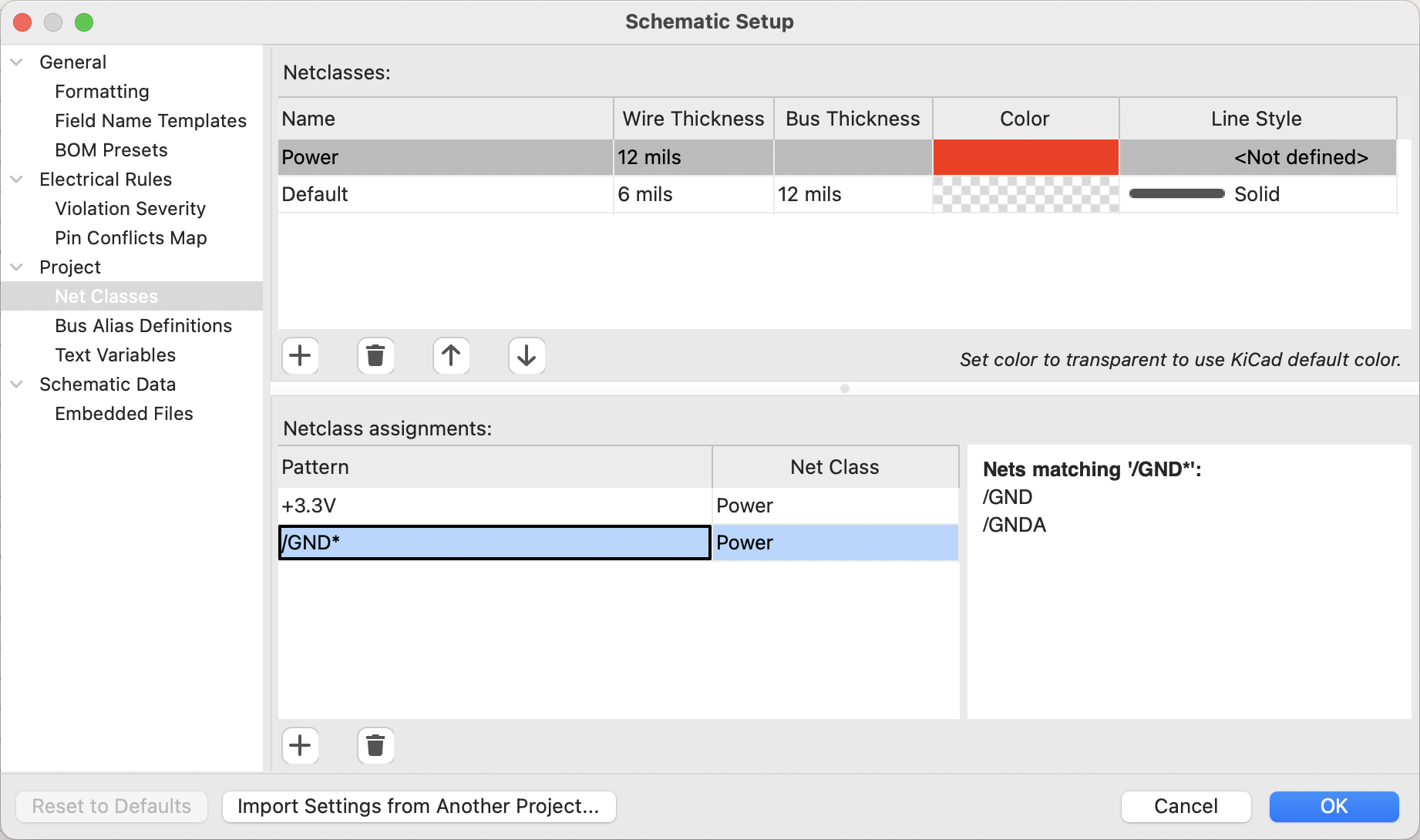
The top pane lists the net classes that exist in the design. The Default net class always exists, and you can add additional net classes with the ![]() button or remove the selected net class with the
button or remove the selected net class with the ![]() button.
button.
Net classes can be moved up and down in priority order with the ![]() and
and ![]() buttons. Note that the
buttons. Note that the Default net class will always be the lowest priority net class and can therefore not be moved.
Each net class can have unique graphic properties that determine how wires of that net class are displayed in the schematic. Wire and bus thicknesses, color, and line style (solid, dashed, dotted, etc.) can all be adjusted. Setting the color to transparent will use the theme’s default wire/bus color for the net class, which is configurable in Preferences. By default any color that is configured for a net class controls the color is used to draw wires in that net class. If the Highlight netclass colors setting is enabled in the Display Options section of the Schematic Editor preferences, this color will instead be used to draw a highlight around wires in that netclass, and the wires themselves will always be drawn with the color scheme’s wire color.
You can also set board design rules for each net class, although the DRC fields are hidden by default. Right click the header row to show or hide additional columns. For more information about setting net class design rules, see the PCB editor documentation.
All net class parameters for user-defined net classes are optional. However, all properties belonging to the Default net class must be set. When a net has more than one net class assigned, the appropriate value for graphic properties or board design rules is taken from the highest priority assigned net class with the relevant value set. If only one net class is assigned which contains missing properties, any missing values will be taken from the Default net class.
The bottom pane lists pattern-based net class assignments. Each row has a net name pattern and a net class; nets with names that match the pattern are assigned to the specified net class. If a net matches multiple patterns, the net is assigned to all of the matching net classes. You can sort the list of net class assignment patterns by pattern or by net class name by clicking on the corresponding column header.
Pattern-based net class assignments are dynamic: when a new net is added that matches an existing pattern, it will be assigned to the associated net class automatically. Net patterns can use both wildcards (* to match any number of any characters, including none, and ? to match any character) and regular expressions. The nets that match the selected pattern are displayed to the right of the pattern list.
例如, net* 模式匹配名为 net , net1, network, 和任何其他以 net 开头的网络名称的网络。 因为 * 在正则表达式中的含义略有不同(* 匹配零个或多个前面的字符), net* 模式也匹配名为 ne 的网络。
记住,网络名必须包括完整的原理图页面路径。例如,一个在根原理图中本地标记的网络有一个以 / 为前缀的名称。
|
Use the ![]() button to add a net class assignment pattern or the
button to add a net class assignment pattern or the ![]() button to remove a pattern.
button to remove a pattern.
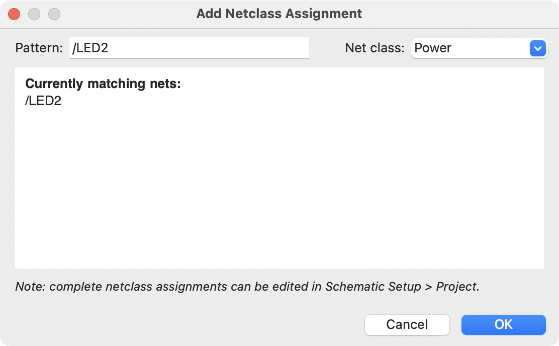
Instead of adding net class patterns in the Schematic Setup dialog, you can directly create net class patterns from the schematic canvas. Right click a net and select Assign Netclass… to bring up the Add Netclass Assignment dialog. The net class pattern is pre-filled with the name of the selected net, but the pattern can be changed if desired. All nets matching the pattern are displayed in the dialog. This method can only be used on nets with an assigned name.
Graphically assigning net classes in the schematic
As an alternative to pattern-based net class assignment, net classes can be graphically assigned to nets in the schematic using either directive labels, net labels, or rule areas.
In the image below, a directive label is used to assign signals to the 50R net class.
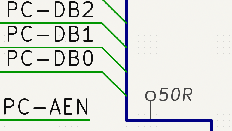
Directive labels are added with the ![]() button in the right toolbar. They behave like labels, except that they cannot be used to name a net. The attached net is assigned a net class according to the value of the directive’s
button in the right toolbar. They behave like labels, except that they cannot be used to name a net. The attached net is assigned a net class according to the value of the directive’s Net Class field. The Net Class field presents a dropdown list of all the net classes that have been specified in Schematic Setup or Board Setup.
You can also type in a net class that isn’t explicitly listed in the Schematic/Board Setup priority list. Such implicit net classes can’t be assigned any design settings, like net class color or track width, but they can still be used in DRC rule queries.
If multiple Net Class fields are added to a directive label, or multiple directive labels with Net Class fields are applied to a net, all of the specified net classes are assigned to the net.
如果一个标识符被附加到一个总线上,总线上的所有成员都被分配到指定的网络类。
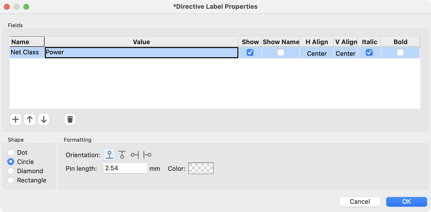
In addition to the associated net class, you can edit the directive’s shape (dot, circle, diamond, or rectangle), orientation, pin length, and color in the directive’s properties.
Net labels can also be used to assign net classes to
nets by adding a Net Class field to the label.
|
The Rule Area tool (![]() ) can be used to draw a shape to which net class directives can be attached. Any wire, bus, label, or symbol pin which crosses or is inside the rule area will be assigned the net class of a net class directive attached to the rule area border. An example is shown in the image below; all wires passing through the rule area will be assigned the
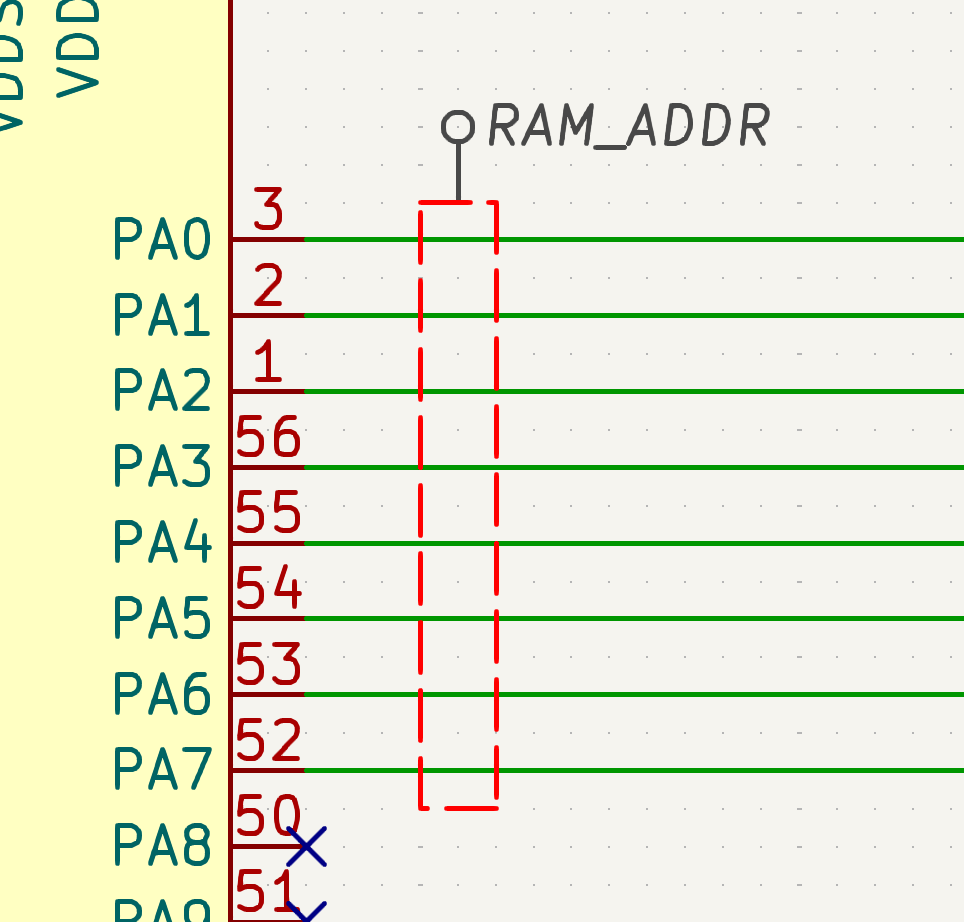
) can be used to draw a shape to which net class directives can be attached. Any wire, bus, label, or symbol pin which crosses or is inside the rule area will be assigned the net class of a net class directive attached to the rule area border. An example is shown in the image below; all wires passing through the rule area will be assigned the RAM_ADDR net class.
You can show or hide directive labels in the schematic using the View → Show Directive Labels option.
Component classes
Component classes are named groupings of components: they are assigned to symbols in the schematic or to footprints in the board, but however they are assigned they apply to both the symbols and the corresponding footprints. They can be used to group symbols into channels for multichannel designs and can also be used to group footprints in custom DRC rules.
To assign a component class to a symbol, you can add a symbol field named Component Class to the symbol. The symbol will then be a member of the component class named by the field.
You can also assign component classes using directive labels (![]() ) in combination with rule areas (
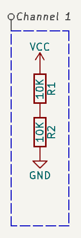
) in combination with rule areas (![]() ). The Rule Area tool can be used to draw a shape to which directive labels can be attached. Any symbol which crosses or is inside the rule area will be assigned to the component class specified by the directive label attached to the rule area border. An example is shown in the image below; R1 and R2 will be assigned to the
). The Rule Area tool can be used to draw a shape to which directive labels can be attached. Any symbol which crosses or is inside the rule area will be assigned to the component class specified by the directive label attached to the rule area border. An example is shown in the image below; R1 and R2 will be assigned to the Channel 1 component class.
Component classes can also be assigned in the PCB Editor by creating rules for automatic component class assignment.
Components can have more than one class, and symbols take on a class if any of their sub-units have that class. If multiple Component Class fields are added to a directive label, or multiple directive labels with Component Class fields are applied to a rule area, the symbols in the rule area will take on all of the specified component classes.
Rule areas
Rule areas are regions of the schematic that apply certain properties to the symbols and nets inside the area.
You can use rule areas to apply any of the following attributes to the symbols inside the rule area:
-
Exclude from simulation
-
Exclude from bill of materials
-
Exclude from board
-
Do not populate
A rule area that has any of those attributes enabled will apply the enabled attributes to all symbols that are fully or partially enclosed by the rule area.
You can also use a rule area, in combination with a directive label, to apply net classes and component classes to symbols and nets inside the rule area. Any wire, bus, label, or symbol pin which crosses or is inside the rule area will be assigned the net class specified by any directive labels attached to the rule area border. Any symbols that are fully or partially enclosed by the rule area will be assigned the component class specified by any attached directive labels.
In the image below, all wires passing through the rule area will be assigned the RAM_ADDR net class.
To draw a rule area, use the Rule Area tool (![]() button).
button).
-
Click in the canvas to begin drawing the rule area outline.
-
Click to place additional corners.
-
Double click to complete the outline.
The rule area tool obeys the selected line mode: the outline is restricted to horizontal, vertical, and 45 degree lines unless free angle mode is enabled.
|
You can switch line modes using Shift+Space or using the |
To use a rule area to assign a net class or component class, you must add a directive label to the rule area.
-
Activate the directive label tool (
 button on the right toolbar). By default, the directive label tool is grouped in a palette with the other label tools and therefore may be hidden.
 -
In the directive label’s properties dialog, set the label’s
Net Classand/orComponent Classfields to the desired net class or component class, respectively. -
Place the directive label in the canvas so that the label’s connection point is on the border of the rule area, as shown in the screenshot above.
To enable attributes (exclude from simulation, exclude from BOM, exclude from board, or DNP) for the rule area, open the rule area’s properties dialog (E). Any attributes that are enabled in the rule area’s properties are applied to symbols that are fully or partially enclosed by the rule area.
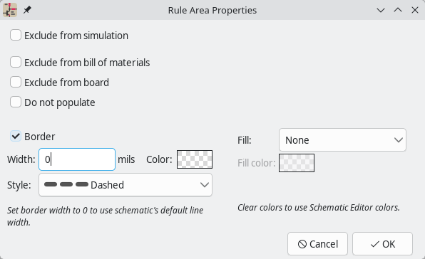
You can also configure the graphical style of the rule area’s border and fill here. The border can be set to any color or line width, and various line styles (solid, dashed, dotted, etc.) are available. If the line width is set to 0, the default line width from the Formatting page of Schematic Setup is used. The fill can be set to None (default), Solid, or one of several types of hatching. You can also configure the fill color. If either the border or fill color is not set, that color is taken from the Rule Areas color in the color theme.
Graphics and text
文字、图形和图像可以被添加到原理图中,用于文档的目的。这些对象对原理图没有任何电气影响。
下面的图片除了符号和几种类型的标签外,还显示了图形线和文字("COMMUNICATION DSP")。
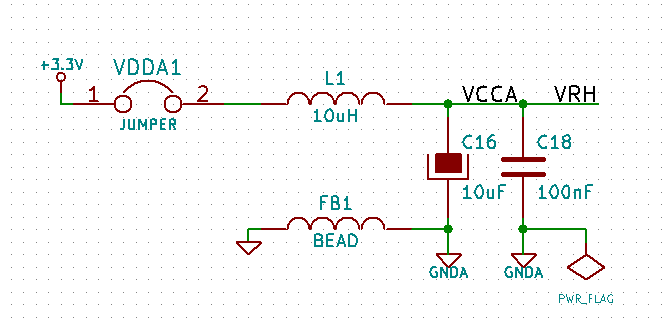
Text and text boxes
Two kinds of text can be added to schematics, which are referred to as text (![]() ) and text boxes (
) and text boxes (![]() ). Both are added using their respective buttons in the right toolbar. Text boxes are similar to regular text except that they have an optional border and they automatically reflow text within that border.
). Both are added using their respective buttons in the right toolbar. Text boxes are similar to regular text except that they have an optional border and they automatically reflow text within that border.
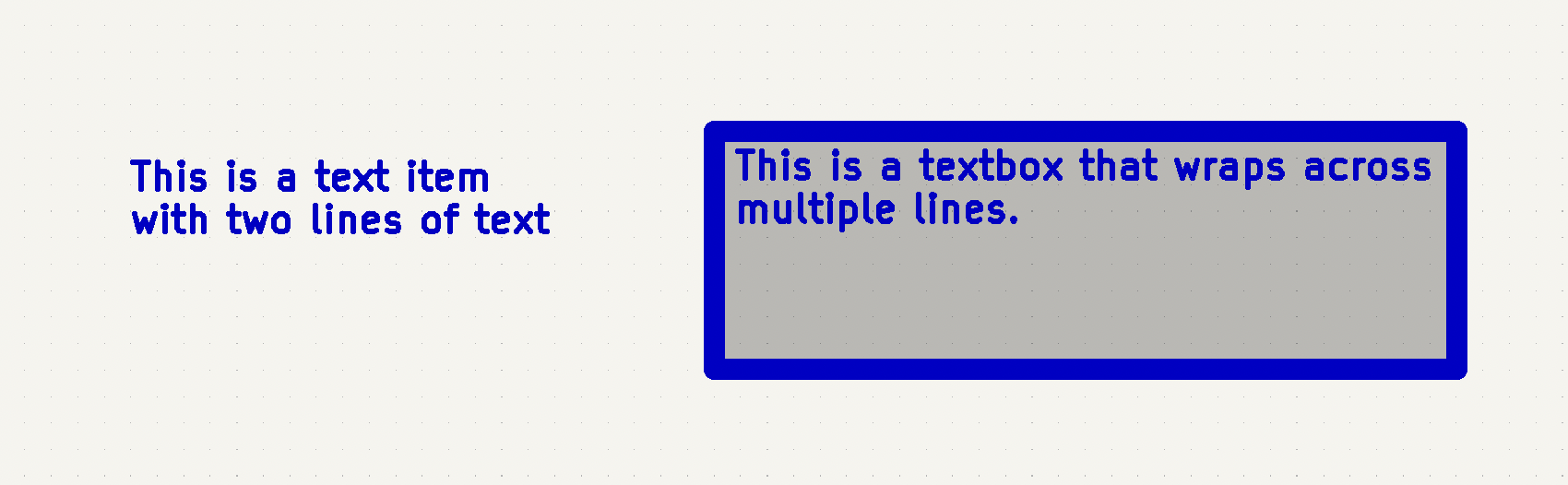
Both kinds of text item support multiline text and basic formatting features, but text boxes wrap text to fit in the outline and have additional formatting options. All text has adjustable fonts, color, size, bold and italic emphasis, left and right alignment, and vertical and horizontal orientation. Text boxes additionally support horizontal centering, vertical alignment options, and colored borders and fill. You can also adjust the padding on each side of text in a text box (padding can be set using the Properties Manager, but not using the Text Box Properties dialog).
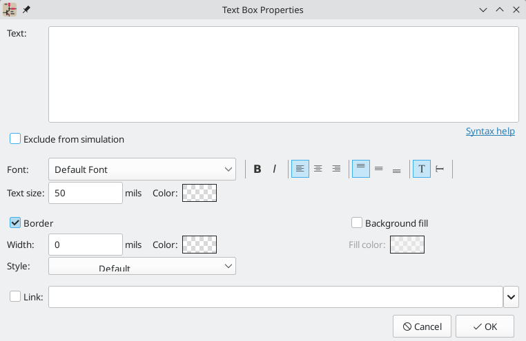
链接
In a text object, text box, or table cell, any text beginning with http:// or https:// is treated as a URL and automatically turned into a link. Clicking on such a link opens the URL in your web browser. If the text contains multiple URLs, each URL is turned into a separate link.
Alternatively, you can explicitly turn an entire text object or text box into a link by entering a target in the Link box in the text properties. This turns the entire text item or text box into a clickable link. Such text can only link to a single URL, but the displayed text can be anything, rather than simply the URL.
You can link to different kinds of resources depending on the link target. The target of an explicit link can be:
-
a sheet in the current schematic, using
#followed by the page number -
a local file on your machine, using a URL with the
file://scheme -
a website, using a URL with the
http://orhttps://scheme -
another resource, using a URL with the appropriate scheme, e.g.
ftp://
If no protocol prefix is used, the target is assumed to be a local file as if the file:// scheme was used.
Sheet, file, and web links can be autofilled using the dropdown meu in the link target box. Other kinds of links cannot be autofilled but will work if your system can handle them.
字体
文本和文本框支持自定义字体,可通过文本的属性对话框中的 字体 下拉选择。除了 KiCad 字体外,你还可以使用安装在你电脑上的任何 TTF 字体。
| 用户字体不会被嵌入工程中。如果该工程在另一台没有安装所选字体的计算机上打开,将会被替换为不同的字体。为了获得最大的兼容性,请使用 KiCad 字体。 |
Text markup
文本标记支持上标, 下标, 评估工程变量和访问符号字段值。
| Feature | Markup Syntax | Result |
|---|---|---|
Superscript |
|
textsuperscript |
Subscript |
|
textsubscript |
Overbar |
|
text |
|
variable_value |
|
|
field_value of symbol refdes |
| Project text variables must be defined in Schematic Setup before they can be used. There are also a number of built-in system text variables. |
Simulation directives
Text and textboxes can contain simulation directives for SPICE simulations. The Exclude from simulation checkbox prevents text from being interpreted as a simulation directive.
Tables
You can use a table to organize text in a tabular format. Tables have customizable borders, cell sizes, colors, and headers.
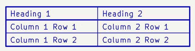
To place a table, use the ![]() button in the right toolbar. Click in the canvas to place the top left corner of the table, then click again to place the bottom right corner of the table and finish drawing the table. The bigger you draw the table, the more rows and columns will be added by default, but rows and columns can be added or deleted after the table is created.
button in the right toolbar. Click in the canvas to place the top left corner of the table, then click again to place the bottom right corner of the table and finish drawing the table. The bigger you draw the table, the more rows and columns will be added by default, but rows and columns can be added or deleted after the table is created.
Once you have created a table, you can edit the table as a whole or edit cells individually. Creating a new table automatically opens the Table Properties dialog to edit the entire table.
You can export a table from KiCad into a CSV file by right clicking a table or table cell and clicking Export Table to CSV….
Editing a whole table
You can edit an entire table with the Table Properties dialog. There are several ways to open the Table Properties dialog:
-
Create a new table. The Table Properties dialog opens automatically when the table is created.
-
Select any cell in the table, right click, and select Edit Table (Ctrl + E).
-
Select the entire table, right click, and select Properties… (E). You can select the entire table with a drag selection or by selecting a single cell, then right clicking and selecting Select Table.
-
Click the Edit Table… button in the Table Cell Properties dialog.
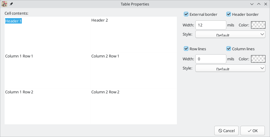
This dialog lets you edit the properties of the entire table, including the text in each cell and the separators between cells. To change the formatting of text in a cell, edit the properties of individual cells, instead of the properties for the entire table.
| The properties for a table can also be edited in the Properties Manager when the entire table is selected. |
The left side of the dialog displays an editable grid of the entire table. You can edit the contents of any cell by clicking on the cell in the grid. You can also edit the text in a cell by selecting the cell and using the Properties Manager. If you have tabular content in a spreadsheet or other table, you can copy and paste that content into the grid here.
| Text in table cells supports the markup described in the text markup section (superscripts, subscripts, strikethroughs, etc.). |
The right side of the dialog contains formatting options for the table.
-
The Locked checkbox controls whether or not the table is locked. Locked objects may not be manipulated or moved, and cannot be selected unless the Locked Items option is enabled in the Selection Filter panel.
-
The External border and Header border checkboxes control whether there is a border drawn around the entire table and the cells in the top row, respectively. When Header border is enabled, the border below the cells in the top row is styled using these external border settings rather than the row/column line settings. The line width of the header borders is controlled by the Width field. When set to 0, the line width uses the default symbol line width configured in the Formatting panel of Schematic Setup. The line color is controlled by the Color picker, and the line style can be set to solid, dashed, dotted, dash-dot, or dash-dot-dot using the Style dropdown menu.
-
The Row Lines and Column lines checkboxes enable horizontal lines between rows and vertical lines between columns, respectively. These have the same formatting options as the external and header borders.
Editing individual table cells
Instead of editing the properties of an entire table, you can also edit the properties of individual cells. This modifies selected cells, but does not affect other cells. To open the Table Cell Properties dialog, double click on a cell, or select a cell, right click, and choose Properties… (E). If you select multiple cells, the properties dialog will act on all of them at once.
| You can select multiple cells by clicking and dragging. |
| To select all cells in a row or column, select a cell in that row or column, right click, and choose Select Row(s) or Select Column(s). You can select multiple rows or columns in this way by starting with multiple cells selected. |
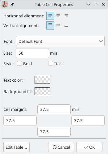
The left side of the dialog lets you edit the contents of the selected cell. The right side of the dialog contains formatting options for the selected cell.
-
Horizontal alignment and Vertical alignment control how text is positioned within the cell.
-
The Font dropdown lets you select a font for the text. You can use any TTF font available on your system, or the built-in KiCad stroke font.
-
Size controls the size of the text in the cell.
-
The Bold and Italic checkboxes bold and italicize the text, respectively. These are three-state checkboxes, which can be set to off, on, or no change. No change is useful when multiple cells with different bold/italic settings are being edited at the same time.
-
The Text color and Background fill color pickers control the color of the text and the cell background, respectively.
-
The Cell margins textboxes control the amount of spacing around the top, bottom, left, and right of the text in the cell.
You can click the Edit Table… button to open the properties dialog for the entire table.
| The properties for a table cell can also be edited in the Properties Manager when one or more table cells is selected. |
Editing table layout
The layout of a table (size and number of columns and rows) is initially set when you create a table, but you can also edit the layout after creation.
To resize a row or column, select a cell in that row or column, then drag the handle on the right (to change the column width) or the bottom (to change the row height) to the desired size.
To add rows or columns, select a cell next to where the new row or column should go, right click, then choose Add Row Above, Add Row Below, Add Column Before, or Add Column After, as desired.
To delete rows or columns, select a cell in the row or column you want to delete, then right click and choose Delete Row(s) or Delete Column(s). To delete multiple rows or columns, start with a selection that spans all the rows or columns you want to delete.
You can merge multiple cells into a single cell by selecting all the cells you want to merge, right clicking, and choosing Merge Cells. To unmerge them, select the merged cell, right click, and choose Unmerge Cells.
Graphic shapes
Graphic rectangles (![]() ), circles (
), circles (![]() ), arcs (
), arcs (![]() ), and lines (
), and lines (![]() ) can all be added using their respective buttons in the right toolbar.
) can all be added using their respective buttons in the right toolbar.

线宽、颜色和样式(实线、虚线或点线)可以在每个图形(E)的属性对话框中进行配置。矩形、圆形和弧形也可以设置填充颜色并去除其轮廓线。
将形状的线宽设置为 0,则使用原理图的默认线宽,该线宽可在 <schematic-setup,原理图设置>> 中配置。虚线的间距也可以在那里配置。移除线条或填充物的颜色将会使用颜色主题的图形颜色,这可以在 偏好设置 中配置。
与导线一样,图形的线条服从线条的绘制模式设置(90 度,45 度,或自由角度),可以用左侧工具栏的切换按钮来设置 (![]() ,
, ![]() , and
, and ![]() )。 Shift+Space 循环切换这些模式。
)。 Shift+Space 循环切换这些模式。
与 PCB 布线一样 ,/ 快捷键切换线条模式。
Importing bitmap images
KiCad supports inserting images into the schematic. These are purely for reference during the design process and play no electrical role.
To add a bitmap image, use the ![]() button on the right toolbar and select the desired bitmap image file. Click in the canvas to place the image.
button on the right toolbar and select the desired bitmap image file. Click in the canvas to place the image.
| You can also import a bitmap image by dragging and dropping it onto the editing canvas. |
Once the image has been added to the canvas, you can reposition it using the move tool (M) or by dragging it in the canvas. You can scale it by dragging the editing handles at the corners of the image. The image is scaled around its reference point; in other words, the reference point is the point in the image that always stays in the same position in the canvas, no matter how the image is scaled. The reference point is shown as a fifth editing handle. Initially it is at the center of the image, but you can reposition the reference point by dragging it in the canvas.
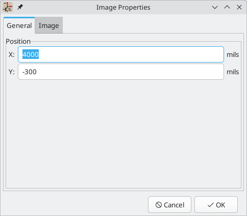
You can also reposition or scale the image in its properties dialog (E). Position and scale in this dialog are relative to the center of the image, not its interactive reference point. You can also Convert to Greyscale if you wish.
Importing vector graphics
You can add graphic shapes from an external vector graphics file by importing the file into KiCad. DXF and SVG files are supported. To import the file, use File → Import → Graphics… (Ctrl+Shift+F).
| You can also import a vector graphics file by dragging and dropping it onto the editing canvas. |
Imported vector graphics are part of the design like any other graphic shape. In other words, they have an assigned board layer, they are included in fabrication outputs, and shapes on copper layers can make electrical connections.
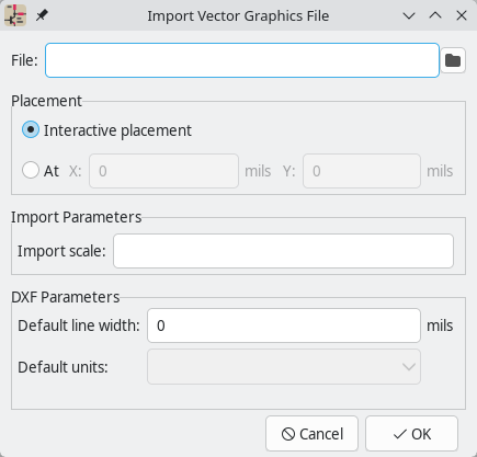
The Import Vector Graphics File dialog has several options:
-
File specifies the vector graphics file to import.
-
If Interactive Placement is selected, you can place the graphics interactively in the canvas after importing. If At is selected, the graphics will instead be placed at the specified coordinates.
-
Import Scale sets the scale factor for the import.
-
DXF default line width sets the line width for any items in a DXF file that do not specify a line width. It has no effect when not importing DXF files.
-
DXF default units sets the default unit for DXF files with unspecified units. It has no effect when not importing DXF files.
批量编辑文本和图形
Properties of text and graphics, including symbol fields, can be edited in bulk using the Edit Text and Graphic Properties dialog (Edit → Edit Text and Graphic Properties…). The tool can also modify visual properties of wires and buses.
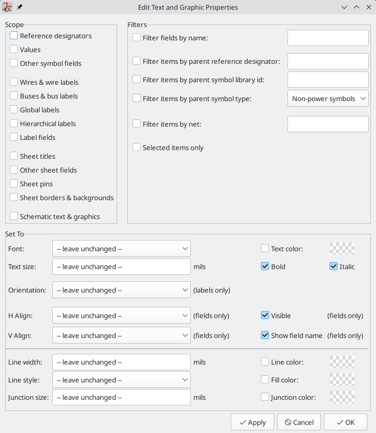
范围和筛选器
Scope settings restrict the tool to editing only certain types of objects. If no scopes are selected, nothing will be edited.
Filters restrict the tool to editing particular objects in the selected scope.
Objects will only be modified if they match all enabled and relevant filters
(some filters do not apply to certain types of objects. For example, symbol
field filters do not apply to wires and are ignored for the purpose of changing
wire properties). If no filters are enabled, all objects in the selected scope
will be modified. For filters with a text box, wildcards are supported: *
matches any number of any characters, including none, and ? matches any single
character.
-
By field name filters to the specified symbol field, label field, or sheet field.
-
By parent reference designator filters to fields in the symbol with the specified reference designator.
-
By parent symbol library id filters to fields in symbols with the specified library identifier.
-
By parent symbol type filters to fields in symbols of the selected type (power or non-power).
-
By net filters to wires and labels on the specified net.
-
Only include selected items filters to the current selection.
可编辑的属性
可以在对话框的底部为被筛选对象的属性设置新值。
Drop-down lists and text boxes can be set to -- leave unchanged -- to preserve existing values. Checkboxes can be checked or unchecked to enable or disable a change, but can also be toggled to a third "leave unchanged" state. Color properties must be checked to change the value; a checkerboard swatch indicates that the color will be inherited from the default value from the the schematic settings or net class properties.
可以修改的文本属性有 字体、文本大小、文本方向(右/上/左/下)、水平 和 垂直对齐、文本颜色、强调(粗体*和*斜体)以及字段和字段名的 可见性。
可以修改的图形和导线属性有:线宽、线样式(实线、虚线和点线)、线颜色、图形的 填充颜色,以及导线结点的 结点尺寸 和 结点颜色。
原理图标题栏
The drawing sheet’s title block is edited with the Page Settings tool (![]() ). You can also open this tool by double clicking anywhere on any part of the drawing sheet.
). You can also open this tool by double clicking anywhere on any part of the drawing sheet.
可以编辑标题栏中的每个字段,以及纸张大小和方向。 如果为某个字段选中了 导出到其他原理图页 选项,则该字段将在所有原理图页的标题栏中更新,而不仅仅是当前原理图页。
You can set the date to today’s or any other date by pressing the left arrow button next to Issue Date. Note that the date listed in the schematic title block is not automatically updated. It is only updated when changed in this dialog.
A drawing sheet file can also be selected to replace the default drawing sheet. When choosing a drawing sheet, you can enable the Embed File checkbox in the file browser to embed the drawing sheet in the schematic instead of referencing an external file. This means the schematic will appear the same when it is opened on another computer that does not have the drawing sheet file available at the same external file path. For more information, see the embedded files documentation.
原理图页码(页面X/Y)会自动更新,也可以用 编辑 → 编辑原理图页码… 手动设置。
Groups
Groups let you treat multiple objects as a single object for the purposes of moving or rotating them. Each object in the group will maintain its position relative to the other objects in the group. When objects are grouped, it is difficult to accidentally edit them or move them relative to the other members of the group. Groups can have a name, which is displayed in the editing canvas when the group is selected.
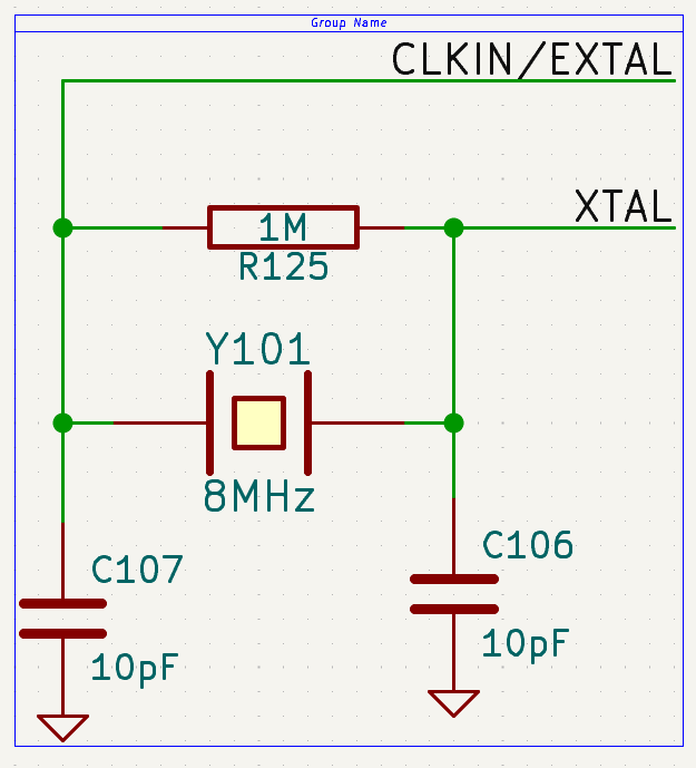
Most types of objects in the Schematic Editor can be grouped: symbols, wires, labels, graphic items, and even other groups. Groups can contain multiple different types of objects at once.
To add objects to a group, select them, then right click and choose Grouping → Group Items, or click the ![]() button in the top toolbar. To remove all items from a group, select the group, right click, and choose Grouping → Ungroup Items, or click the
button in the top toolbar. To remove all items from a group, select the group, right click, and choose Grouping → Ungroup Items, or click the ![]() button in the top toolbar.
button in the top toolbar.
Once objects have been added to a group, selecting any of the objects will select the group as a whole instead of the constituent objects. To edit a specific object within a group, first select the group, the right click and choose Enter Group. Double clicking on a group also enters the group. When a group has been entered, objects within the group can be selected and edited individually without affecting the other objects in the group. To leave the group and stop editing its members individually, right click and select Leave Group, select an object outside the group, or use Esc.
There are several ways to modify which objects belong to a group. To remove objects from an existing group, enter the group, then select the objects you want to remove, right click, and choose Grouping → Remove Items. To add items to a group, first ungroup all the items from the group. This will leave the group’s former members selected. Then add the new item to the selection and group the selection. Note that without first ungrouping, this process would create a nested group: a new group containing the new item and the entire original group, not just the items in the original group.
You can also add or remove objects from a group in the group’s properties dialog. To open a group’s properties dialog, press E or right click and click Properties…. The properties dialog lists the objects contained in the group. To add an additional object to the group, click the ![]() button, then click on the desired object in the editing canvas. The object you click on will be added to the group. To remove an object, select it in the list, then click the
button, then click on the desired object in the editing canvas. The object you click on will be added to the group. To remove an object, select it in the list, then click the ![]() button.
button.
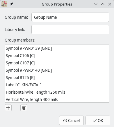
The Library link field is used for design blocks. It specifies the group’s linked design block name and library in the format <library>:<block>. This field must be filled out correctly to link design block schematic groups to the corresponding block in the board and in the design block library.
You can optionally transfer groups from the schematic to the PCB using the Update PCB from Schematic tool. If the Group footprints based on symbol group option is enabled, footprints in the PCB will be grouped if their linked symbols are grouped in the schematic.
Aligning objects
The align tool moves a selection of objects so that they are all aligned with a reference object. There are six different alignments to choose from, depending on which part of the objects you wish to align. Objects can be horizontally aligned by their left, center, or right edges, or they can be vertically aligned by their top, center, or bottom edges. Objects are only moved in one dimension, so objects stay in the same horizontal position when aligned vertically, and vice versa. To align objects by a given edge, select the objects, then right click and choose Align/Distribute → Align to Left (or another alignment as desired).
If the cursor is over an object in the selection, that object is used as the reference object. Otherwise, the reference object is the object in the selection which is located furthest in the alignment direction, for example the leftmost object when aligning by left edge, or the topmost object when aligning by top edge. The topmost object is used when aligning by vertical center, and the leftmost when aligning by horizontal center.
Before alignment
After alignment
In the example above, two circles are vertically aligned by their top edges, with the large circle as the reference object. The first image shows them before alignment and the second image shows them after alignment. In this case, the large circle is the topmost object before alignment, so it is chosen as the reference object if the cursor is not over the other circle. After alignment, the top edges of the circles are at the same position, but the horizontal positions of the circles are unchanged.
| Symbols, labels, and other objects with pin connections are always moved so that their connection points remain on the grid, even if this results in imperfect alignment with the other objects. |
Schematic editing convenience functions
There are several convenience features in the Schematic Editor that make some common editing and connection operations faster.
Pin helpers
You can quickly add wires, labels, or no-connection markers to a selection of pins using the Pin Helpers tools in the right-click context menu. This can help you quickly break out unconnected pins from a symbol or hierarchical sheet. By selecting Pin Helpers → Wire, the wire tool will begin drawing a wire from all selected pins at once. If you select No Connect, no-connection markers will be added to the end of each selected pin. And if you choose Net Label, Hierarchical Label, or Global Label, a label of the respective type will be placed at the end of each selected pin. Each label’s name will be set to the corresponding pin name. The new labels will remain selected, so you can easily move them away from the symbol using M or G, depending on whether you wish to maintain a wired connection between the pins and the labels.
| Pin helpers require you to select individual pins, not their parent symbol or sheet. Symbol pins cannot be individually selected if the clicking on a pin selects the symbol option is enabled in the Editing Options pane of the Schematic Editor preferences. Therefore, this option must be disabled to use the Pin Helper tools. |
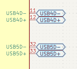
Converting between object types
Existing labels and text objects can be changed to another type of label or text by right clicking the object(s) and selecting the target object type from the Change To submenu. The allowed types for source and target objects are local labels, global labels, hierarchical labels, directive labels, text objects, and text boxes. The value of the original object is preserved in the resulting object: when a text object is converted to a label, the label’s value (net name) will be the original text, and vice versa.
Swapping objects
You can swap the position of two selected objects using the Swap command (Alt+S; also available in the right-click context menu). This works on many schematic items, including symbols, symbol fields, labels, graphical items, and text. The first object is assigned the location and rotation of the second object, and vice versa. If there are more than two objects selected, the locations are cycled: the last object gets the position of the first object, the first object gets the location of the second, and so on.
| One possible use of the swap command is to exchange two units within a symbol, for example the two amplifiers in a dual op-amp. You could also use swap with a selection of labels to modify net assignments to symbol pins. These tasks, and other related operations, can be quickly accomplished using the pin swap and gate swap functions, which work similarly to the generic swap command but are focused on swapping labels, pins, and gates. |
Swapping pins and pin labels
Pin swapping exchanges the assigned nets between a selection of symbol pins, so that the net that was assigned to one pin is moved to a different pin, and vice versa. For example, this could be used to swap the connections between two GPIO pins on a microcontroller. The pins must be part of the same symbol, but otherwise there are no restrictions on which pins can be used in a pin swap.
Pin swaps are unconstrained, which means that KiCad allows you to swap any pins. The tool does not check that the swapped pins are equivalent.
| It is up to you to ensure that the new pin connections are valid after a pin swap. |
There are two forms of pin swapping in the Schematic Editor.
-
Swap the labels connected to each pin by selecting the pins, right clicking, and choosing Swap Pin Labels.
-
Swap the pins, leaving the connected wires/labels in the same place but changing the locations of the pins themselves, by selecting the pins, right clicking, and choosing Swap Pins. This modifies the pin locations in the symbol itself (this modifies the schematic’s copy of the symbol but does not affect the library symbol).
Because the Swap Pins tool modifies symbols in the schematic, it is not available unless the Allow unconstrained pin swaps option is enabled in the Editing Options page of the Schematic Editor preferences. If this option is not enabled, pin labels can be swapped, but pins themselves cannot.
Both forms of pin swapping result in the nets being exchanged between the selected pins. If there are more than two objects selected, the locations are cycled: the last object gets the position of the first object, the first object gets the location of the second, and so on.
Gate (unit) swaps
Gate swaps exchange the connections between two or more units ("gates") of the same multi-unit symbol. All of the nets attached to one symbol unit’s pins are exchanged with the corresponding nets from another unit of the same symbol. For example, this could be used to swap between two opamp units in the same package, or two resistors in a resistor array. In this context, gate refers to to a symbol unit.
Gate swaps are unconstrained, which means that KiCad allows you to swap any units. The tool does not check that the swapped units are equivalent.
You can perform gate swaps in two ways.
-
Swap the units themselves by selecting the units, right clicking, and choosing Swap (Alt+S). In this case, the symbol units exchange places, but the surrounding connections are not changed. Use this option when you don’t want to disturb the schematic connections surrounding each symbol unit.
Swapping units in this way is equivalent to manually changing the unit for each unit you wish to swap. Another fast way to swap symbol units is to right click a single unit and choose another unit from the Symbol Unit submenu. If the new unit was already placed, KiCad will give you the option to swap the units. -
Swap the labels on each unit, while keeping the symbol units themselves in the same place, by selecting the units, right clicking, and choosing Swap Unit Labels. This can only be used when each pin of the symbol unit is connected to a single net label and nothing else. If the schematic connections to the pins are not merely net labels, use the other option instead. This function can also only be used on units that are part of the same symbol and have the same number of pins.
原理图设置
The Schematic Setup window is used to set schematic options that are specific to the currently active schematic. For example, the Schematic Setup window contains formatting options, electrical rule configuration, net class setup, and schematic text variable setup.
To open Schematic Setup, use File → Schematic Setup… or press the ![]() button in the top toolbar.
button in the top toolbar.
原理图格式
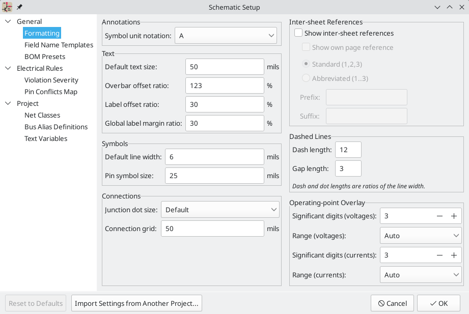
格式化面板包含符号、文本、标签、图形和导线的外观设置。
Symbol unit notation sets how each unit of a multi-unit symbol is referred to
in its reference designator. By default, a different letter for each unit is
appended to the reference designator with no separator, for example U1B for
the second unit of symbol U1, but this can be changed. Numbers can be used
instead of letters, and various separators can be used between the symbol
designator and the unit identifier (., -, _, or none).
Default text size sets the default text height used by the text, text box, and
label tools. Overbar offset ratio controls the vertical spacing between text
and an overbar (~{}) over that text, as a ratio of the text height.
Label offset ratio controls the vertical spacing between a local label’s text
and the attached wire, relative to the label’s text size. This also affects the
spacing between symbol pins and their pin number. Global label margin ratio
defines the size of the box around a global label, relative to the global
label’s text size. Increasing the margin may be useful to avoid overlapping text
with overbars (~{}) or letters with descenders, but this may cause closely
packed global labels to overlap with each other.
Default line width sets the default line width for symbol graphics, if the symbol does not override the default line width. Pin symbol size scales symbol pin graphic style annotations, such as the bubble on an inverted pin.
Hop-over size sets the size of wire hop-overs, which are optionally drawn when one wire crosses another wire without connecting. By default the size is set to None, which means hop-overs are not drawn.
Junction dot size sets the schematic’s default wire junction dot size. The default size can be overridden by editing an individual junction dot’s properties. Connection width specifies the grid size used for the Symbol pin or wire end off connection grid ERC check. Schematics typically use a 50 mil grid for electrical connections, so this should usually remain set at 50 mils.
The Operating Point Overlay settings configure how operating point simulation annotations are displayed on the schematic canvas. The significant digits settings control the number of significant digits printed on voltage and current overlays. The range settings control the units used to display voltage and current measurements.
Show inter-sheet references enables or disables the display of
inter-sheet references, which are a list of page
numbers next to a global labels that link to other places in the schematic where
the same global label appears. Show own page reference controls whether the
current page is included in the list of page numbers. Standard and
abbreviated determine whether to display the complete list of page numbers or
only the first and last page numbers. The prefix and suffix fields add
optional characters before and after the list of page numbers. In the image
of an inter-sheet reference below, a prefix and suffix of [ and ],
respectively, have been added.
虚线外观在格式部分中控制。 虚线长度 控制破折号的长度,而 间隙长度 控制破折号和点之间的间距。 破折号和间隙长度是相对于线宽的:间隙长度为 2 则表示线宽的两倍。
Annotation options
The Annotation panel contains settings for how symbols are annotated.
Symbol unit notation sets how each unit of a multi-unit symbol is referred to
in its reference designator. By default, a different letter for each unit is
appended to the reference designator with no separator, for example U1B for
the second unit of symbol U1, but this can be changed. Numbers can be used
instead of letters, and various separators can be used between the symbol
designator and the unit identifier (., -, _, or none).
The Order and Numbering sections control how symbols are automatically annotated.
-
当同时添加多个符号时,它们会根据 顺序 设置进行批注,按 X 或 Y 位置排序。
-
The Numbering option sets the starting number for new reference designators. This can be the lowest available number, or a number based on the sheet number. When Allow reference reuse is enabled, reference designators can be automatically assigned as long as they are not currently used by another symbol. When disabled, a reference designator can never be used again once it has been assigned to a symbol, even if it is not currently in use.
字段名称模板
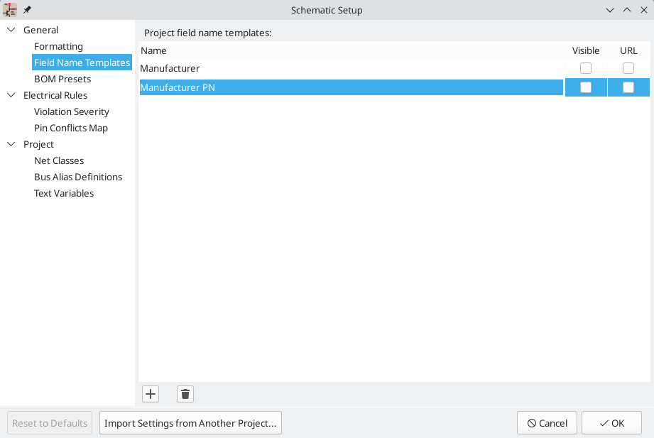
字段名称模板是空的符号字段,会自动添加到原理图中的所有符号。 当原理图中的每个符号都需要在符号中定义的默认字段之外的其他字段时,这可能很有用,例如制造商部件号的字段。
模板字段可以设置为可见或不可见,也可以设置为URL 字段。
在原理图设置中定义的字段名称模板仅适用于当前项目。 字段名称模板也可以在偏好设置中定义,它适用于在您的计算机上编辑的所有项目。
BOM presets
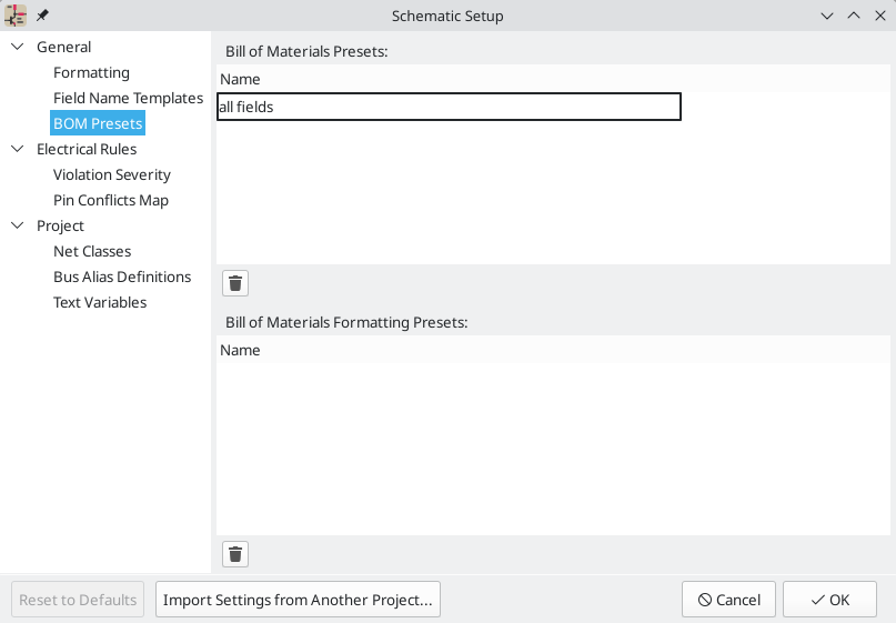
BOM presets are saved configurations for the Symbol Fields Table and BOM export tool. There are two types of presets. BOM presets configure which fields are displayed in the symbol fields table, which order they are displayed in, and how they are used to group symbols. These fields are also directly used in the BOM output. BOM formatting presets configure the output BOM file format, including which separator characters are used to separate fields. Both types of presets are created in the Symbol Fields Table, but can are listed and can be deleted here.
ERC 违规严重性和管脚冲突映射
违规严重性 面板可让您配置应将哪些类型的 ERC 消息报告为错误、警告或忽略。
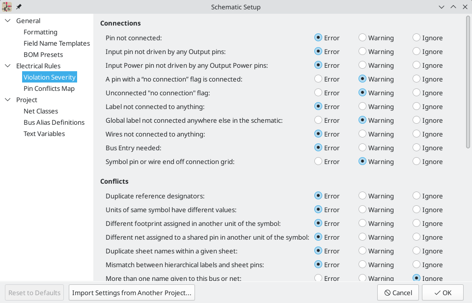
引脚冲突映射 允许您配置连接规则,以根据相互连接的引脚类型定义错误和警告的电气条件。 例如,默认情况下,当输出引脚连接到另一个输出引脚时会产生错误。
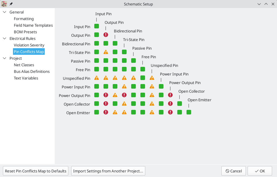
这些面板在 [ERC - 配置,ERC 章节] 中有更详细的解释。
网络类
The Net Classes panel allows you to manage net classes for the project and assign nets to net classes with patterns. Managing net classes in this panel is equivalent to managing them in the Board Setup dialog. Nets can also be assigned to net classes in the schematic using graphical assignments with net class directives or net labels.
Pattern-based net class assigment is explained in more detail in the net classes section.
文本变量
Text variables can be created in the Text Variables section. KiCad will substitute the variable name with the text string assigned to the variable. This substitution happens anywhere the variable name is used inside the variable replacement syntax of ${VARIABLENAME}.
For example, you could create a variable named VERSION and set the text substitution to 1.0. Now, in any text object in the schematic, you can enter ${VERSION} and KiCad will display this as 1.0. If you change the value to 2.0, every text object that includes ${VERSION} will be updated automatically. You can also mix regular text and variables. For example, you can create a text object with the text Version: ${VERSION} which will be displayed as Version: 1.0.
文本变量也可以在 电路板设置中创建。 文本变量是项目范围的; 在原理图编辑器中创建的变量在电路板编辑器中也可用,反之亦然。
还有一些内置系统文本变量。
Embedding files
External files can be embedded within a schematic. Embedding a file stores a copy of the file inside the schematic file. The design can then refer to the embedded copy of the file instead of the external file, which makes the project more portable as it doesn’t rely on an external file. Fonts, datasheets, drawing sheets, SPICE models, and footprint 3D models can be embedded and used within KiCad. Other arbitrary files can also be embedded to store them in the project for later export, but they are not used by any KiCad functionality. Files embedded in a schematic necessarily increase the schematic’s file size, although files are compressed before being embedded to minimize the space required.
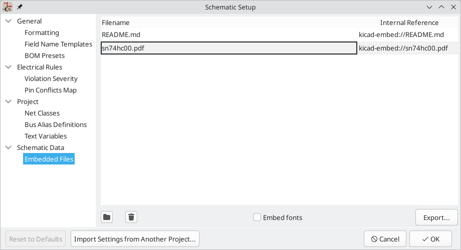
Embedded files are managed in the Embedded Files section of Schematic Setup. All files embedded in a schematic are shown here. To embed a file inside a schematic, click the ![]() button and select the file. The file is then embedded inside the schematic and is listed in the embedded files list along with its embedded reference. The embedded reference is a unique identifier for the embedded file that begins with
button and select the file. The file is then embedded inside the schematic and is listed in the embedded files list along with its embedded reference. The embedded reference is a unique identifier for the embedded file that begins with kicad-embed://. You can use the embedded reference elsewhere in the Schematic Editor to refer to the embedded file as if it were an external file path. You can copy the embedded reference by right clicking and selecting Copy Embedded Reference. To remove an embedded file, click the ![]() button. Any remaining links to the removed file will become invalid.
button. Any remaining links to the removed file will become invalid.
| Datasheets, SPICE models, and drawing sheets can be embedded directly using the file browser when you add them to a symbol (datasheets and SPICE models) or to a schematic (drawing sheets) by enabling the Embed Files option in the file browser. This is a single-step shortcut for adding the files in Schematic Setup and then referring to them by their embedded reference; the result is the same. |
To embed any fonts used in a schematic, check the Embed fonts checkbox. All fonts used in the schematic will be embedded, so text using that font can be edited on any computer regardless of whether the font file is installed.
You can also embed files in a symbol. Such files will be available within the symbol, but not within the larger schematic or in other symbols. Files embedded in a symbol are deduplicated when the symbol is added to a schematic: if a file is embedded in a symbol, and multiple instances of that symbol are added to the schematic, only one copy of the file will be embedded, and all of the symbol instances will refer to the same embedded file.
As an example, to embed a datasheet in a project and use it within several symbols, you could embed the datasheet using the schematic setup dialog, copy the internal reference, and paste the internal reference into the datasheet field of each symbol that uses that datasheet. Each symbol would then have a portable reference to the embedded datasheet. Alternatively, you could embed the datasheet within the library symbol. In this case, each symbol will already have the datasheet embedded when the symbol is added to a schematic. A more convenient way to achieve the same thing, however, is to open the symbol’s properties dialog, browse for a datasheet file, and enable the Embed File option in the file browser. Again, this could be done for a symbol in the schematic or for a symbol in the source symbol library.
Files can also be embedded in boards.
Importing settings
You can import some or all of the schematic setup from an existing schematic. This allows you to choose a schematic to use as a template and select which settings to import.
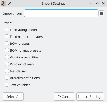
To import settings, click the Import Settings from Another Project… button at the bottom of the Schematic Setup dialog and then choose the .kicad_sch file you want to import from. Select which settings you want to import and the current settings will be overwritten with the values from the chosen schematic.
The settings that are available to import are:
-
Formatting preferences
-
Annotation preferences
-
字段名称模板
-
BOM presets
-
BOM format presets
-
Violation severities
-
Pin conflict map
-
网络类
-
总线别名的定义
-
文本变量
Opening legacy schematics
Modern versions of KiCad can always open projects created in older versions of KiCad. However, schematics created in some older versions of KiCad have special considerations that must be observed when opening them in order to prevent any data loss.
Opening KiCad 5.0 and 5.1 schematics
Modern versions of KiCad can open schematics created in versions prior to KiCad 6.0, but the cache library file (<projectname>-cache.lib) must be present to load the schematic correctly.
Since version 6.0, KiCad stores all symbols used in a project in the schematic. This means that you can open a schematic made in KiCad 6.0 or later on any computer, even if the libraries used in the project are not installed or have changed. Modern KiCad schematic files use the .kicad_sch extension.
Prior to version 6.0, KiCad did not store symbols in the schematic. Instead, KiCad stored references to the symbols and their libraries. It also stored a copy of every symbol used by the project in a separate cache library file (<projectname>-cache.lib). As long as the cache library was included with the project, the project could be distributed without the system library files, because KiCad could load any needed symbols from the cache library as a fallback if the libraries referenced in the schematic were missing. Legacy KiCad schematic files use the .sch extension.
When you open a legacy schematic, KiCad will look in the cache library to find all of the symbols used in the schematic in the cache library. When you save the legacy schematic, KiCad will save it as a new file in the modern schematic format (.kicad_sch), with the necessary symbols embedded in the schematic itself. The original legacy schematic and the cache library will remain, unmodified, but they are no longer necessary once the schematic has been saved in the modern format.
| Projects created in KiCad prior to version 6.0 must have a cache library. If the cache library is missing, the schematic will lose symbol information if the system symbol libraries are modified, reorganized, moved, or deleted. The libraries included with legacy versions of KiCad are substantially different than the modern KiCad libraries, so in practice KiCad will almost always fail to open legacy projects unless the cache library is present. |
When you open a legacy schematic, KiCad may display the Project Rescue Helper dialog. This means that one or more symbols in the cache library do not match the corresponding symbol in the external library. The dialog helps you "rescue" symbols from the cache library into your schematic, if desired. You can also open the rescue dialog at any time using Tools → Rescue Symbols…. The cache library file must be present in order to use the rescue tool.
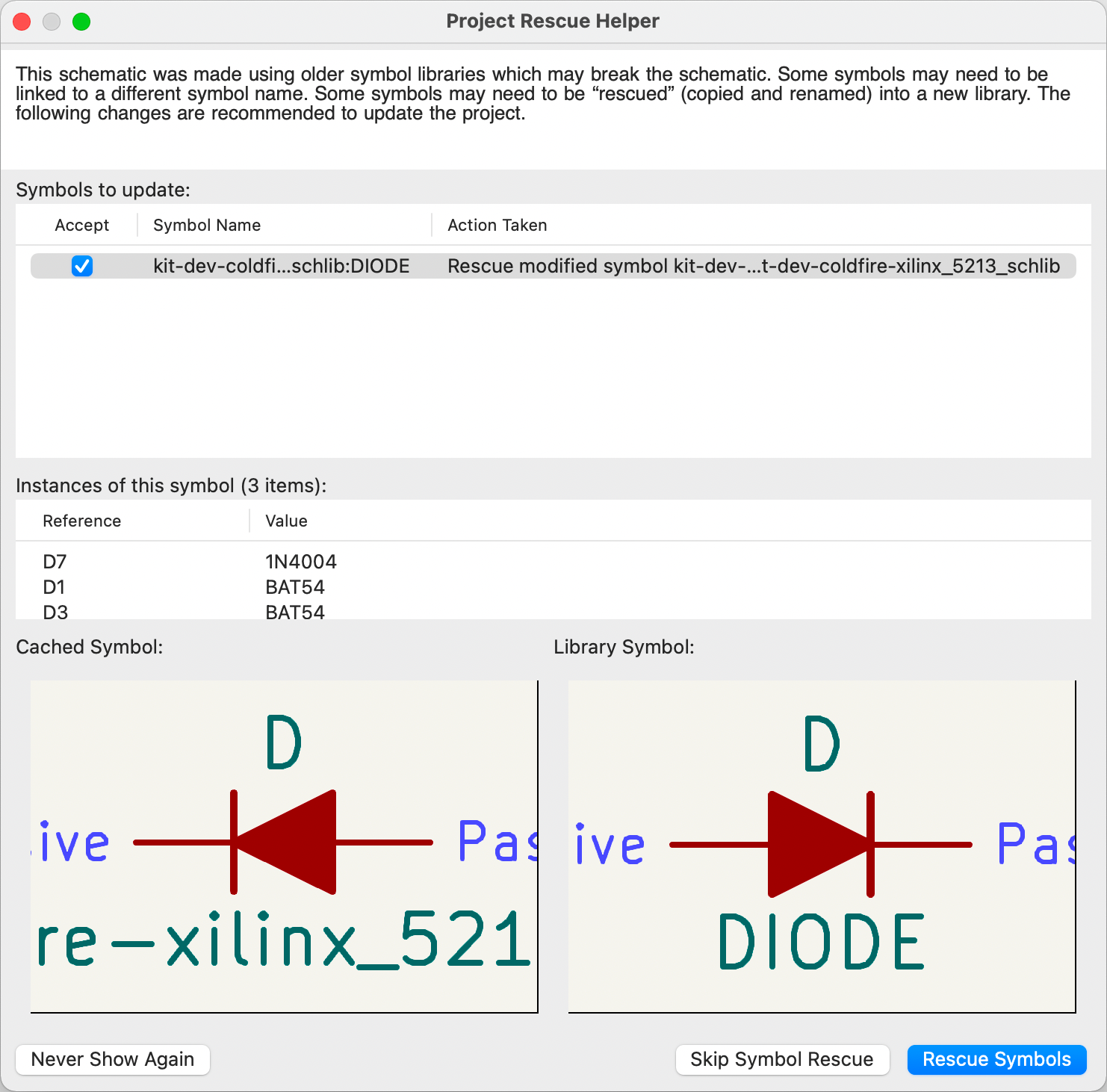
The rescue dialog lists all symbols that don’t match between the cache library and the external symbol library. The discrepancy can be because:
-
the cached symbol or the library symbol has been modified, so the two symbols no longer match, or
-
the cached symbol does not have a corresponding symbol in the symbol library, because the symbol or library was moved, renamed, deleted, or is not present on the current computer.
For each symbol in the list, selecting the symbol displays the reference designator and value for each instance of the symbol, and shows a visual preview of the symbol. If a corresponding symbol exists in the system symbol library, the dialog shows both copies of the symbol for comparison. If the symbol only exists in the cache library, the dialog only shows the cached symbol.
In this example, the project originally used a diode with the cathode facing left, but the library now contains one with the cathode facing right. This change would break the design, so it would be important to use the cached symbol as the original designer intended.
Pressing Rescue Symbols here will cause the selected symbols from the cache library to be saved into a special rescue library (<projectname>-rescue.kicad_sym). The corresponding symbols in the schematic will be updated to use the newly rescued symbols. Any unselected symbols will not be rescued, but their symbol linkage can be updated in the schematic later.
Alternatively, pressing Skip Symbol Rescue will exit the dialog without rescuing any symbols. KiCad will use the versions of the symbols found in the external libraries. You can run the rescue function again with Tools → Rescue Symbols…, or manually edit symbol linkage in the symbol’s properties.
If you would prefer not to see this dialog, you can press Never Show Again. This has the same effect as pressing Skip Symbol Rescue for the current schematic and all future schematics.
If a symbol in a legacy schematic cannot be found in either the cache library or the external library, KiCad cannot rescue that symbol. A placeholder symbol is inserted into the schematic in its place, as shown below.
You can attempt to remap these orphaned symbols using the Change Symbols or Edit Symbol Library Links dialogs, but either option may require manual corrections to the schematic. These tools are explained in more detail in the Updating and exchanging symbols section.
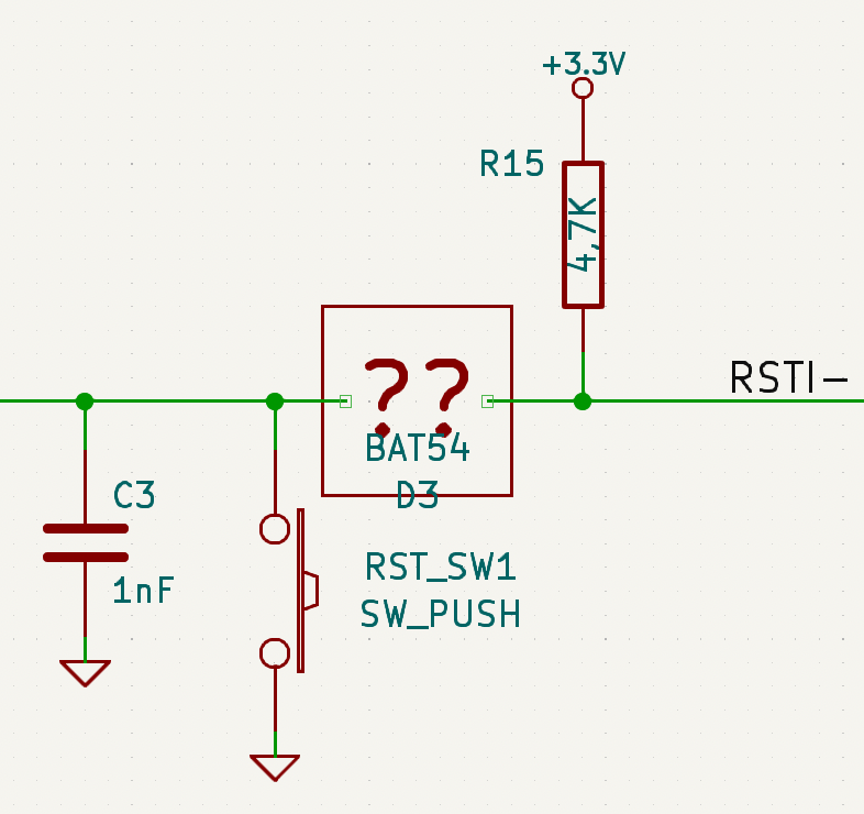
Opening pre-5.0 schematics
Modern versions of KiCad can open schematics created in versions prior to KiCad 5.0, but you will need to go through a symbol remapping process to open the schematic without losing symbol information.
Since version 5.0, KiCad schematics refer to specific symbols using both the symbol and library name. Even if multiple libraries each contain a symbol with the same name, the designer’s intended symbol is unambiguously specified.
Prior to version 5.0, KiCad schematics stored only the symbol name, not the library name. Symbols in the schematic were indirectly mapped back to the original library by searching through the project’s library list for a matching symbol. When you open a pre-5.0 schematic, KiCad will attempt to automatically "remap" the symbols so that each bare symbol name is replaced with a fully-specified symbol library and symbol name pair. The original schematics will be backed up in a rescue-backup folder.
You can skip the automatic remapping, but you will need to remap the symbols yourself using the Change Symbols dialog. You can also re-run the Remap Symbols tool using Tools → Remap Legacy Library Symbols….
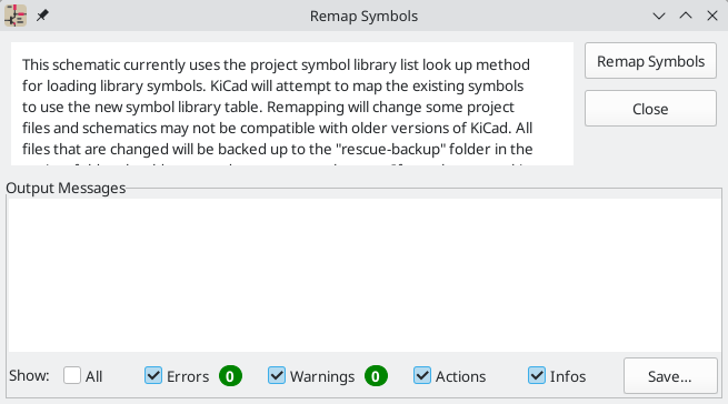
Multiple sheets and hierarchical schematics
Schematics can contain multiple sheets, which can be arranged and connected to each other in several ways. Schematic sheets are organized in a hierarchy, with some sheets organized at the top level of the hierarchy ("top-level sheets"), and others organized as subsheets of top-level sheets or other subsheets ("hierarchical sheets"). Hierarchical sheets are drawn inside another sheet and are organized under that sheet in the schematic hierarchy. Hierarchical sheets can be included in a hierarchy multiple times, if desired.
| Before KiCad 10.0, all multi-sheet schematics in KiCad were hierarchical. Schematics could only have a single top-level sheet, and all other sheets were created as subsheets of the root sheet or other subsheets. Beginning in KiCad 10.0, schematics can have multiple top-level sheets. |
Creating a multi-sheet schematic starts from the first sheet. The process is to create a new sheet, either as a top-level sheet or a hierarchical sheet, then draw the circuit in the subsheet and make the necessary electrical connections between sheets. Connections can be made between nets in different sheets using global labels. For hierarchical sheets, you can also make connections from a subsheet to the parent sheet using hierarchical labels and hierarchical sheet pins.
Carefully considering the best way to organize sheets in a schematic, including whether to draw the schematic hierarchically, improves schematic legibility and reduces repetitive drawing.
Adding top-level sheets to a design
The most basic way to add new sheets to a design in KiCad is to add new top-level sheets. This puts new sheets at the same level of the hierarchy as the existing root sheet, creating a flat schematic where sheets are at the same level rather than nested. Unlike hierarchical subsheets, top-level sheets are not subsheets and are not displayed as sheet symbols in another sheet. You cannot make hierarchical connections between top-level sheets; net connections between top-level sheets can only be made using global labels and global power symbols. Each top-level sheet is saved as a separate .kicad_sch file.
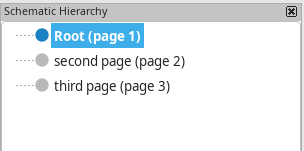
To create a new top-level sheet, right click in the Schematic Hierarchy panel and choose New Top-Level Sheet (if the Schematic Hierarchy panel is not shown, you can show it with View → Panels → Hierarchy Navigator). After choosing a sheet name for the new sheet, the sheet is added to the hierarchy. You can choose a new page number for the sheet by right clicking it in the hierarchy and choosing Edit Page Number or rename the sheet by right clicking and choosing Rename.
Adding hierarchical subsheets to a design
Another way to add additional sheets to a design is using hierarchical subsheets. Subsheets are drawn as a sheet symbol inside of another sheet. The new subsheet is placed beneath the parent sheet in the sheet hierarchy. A net in a sheet can be connected to a subsheet, and vice versa, through a hierarchical sheet pin at the parent sheet level and a matching hierarchical label in the subsheet. Like top-level sheets, each new hierarchical subsheet is saved as a separate .kicad_sch file.
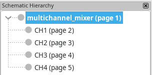
When you add a hierarchical subsheet, you can either create a new sheet or reuse an existing sheet. By reusing an existing sheet, you can use the sheet multiple times in a design. The existing sheet file is used for each instantiation; no new sheet file is created when it is reused. Any edits to the contents of one hierarchical sheet instantiation also affect the other instantiations. The only thing that varies between instantiations of a hierarchical sheet are the reference designators of the symbols in the sheet, which are unique between instantiations.
| 原理图文件可以在多个工程之间共享,以允许在工程之间的设计复用。然而,对路径可移植性的考量,以及在编辑共享图纸时无意中改变其他工程的风险,不建议这样做。 |
You can add a hierarchical subsheet to a design with the Add Hierarchical Sheet tool (S hotkey, or the ![]() button in the right toolbar). Launch the tool, then click twice in the canvas to draw the upper left and lower right corners of the subsheet symbol (you can also click and drag). Make the sheet outline large enough to fit the hierarchical pins you will add later.
button in the right toolbar). Launch the tool, then click twice in the canvas to draw the upper left and lower right corners of the subsheet symbol (you can also click and drag). Make the sheet outline large enough to fit the hierarchical pins you will add later.
原理图属性对话框将出现,并提示输入原理图名称和文件名。
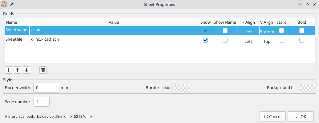
The sheet name must be unique, as it is used in the full net name for any nets in the subsheet. For example, a net with the local label net1 in the sheet sheet1 would have a full net name of /sheet1/net1. The sheet name is also used to refer to the sheet in various places in the GUI, including the title block and the hierarchy navigator. The sheet name can also be changed in the hierarchy navigator.
Sheetfile 原理图文件指定将被保存或加载的原理图文件。原理图文件的路径可以是相对的或绝对的。通常最好是将子原理图文件保存在工程目录中,并使用相对路径,这样便于工程的移植。
通过为每个重复的原理图指定相同的文件名,一个原理图文件可以在一个工程中使用多次;原理图中绘制的电路将在每次使用时被实例化一次,任意实例中的任何编辑都将反映在其他实例中。
The sheet’s page number is configurable here. The page number is displayed in the sheet title block and the hierarchy navigator, and sheets are sorted by page number in the hierarchy navigator and when printing or plotting. The sheet number can also be changed in the hierarchy navigator or for the current page with Edit → Edit Sheet Page Number….
Other attributes for sheets are Exclude from simulation, Exclude from bill of materials, Exclude from board, and Do not populate. When any of these attributes are set for a sheet, they are inherited by all symbols in that sheet, as if they were set on the symbols themselves.
还有几个图形选项可用。边界宽度 设置图纸形状周围的边界宽度。边界颜色 和 背景填充 分别设置图纸形状的边界和填充的颜色。如果没有设置颜色,就会显示一个棋盘式的色块,并使用颜色主题的默认值。
原理图页支持任意自定义字段,可以分别使用 ![]() 和
和 ![]() 按钮添加和删除。 通过选中它们的 显示 框,可以选择在原理图上显示页面字段,并且可以使用 文本变量 从图纸内部或其他图纸字段中访问它们。
按钮添加和删除。 通过选中它们的 显示 框,可以选择在原理图上显示页面字段,并且可以使用 文本变量 从图纸内部或其他图纸字段中访问它们。
通过选择一个页面符并使用 E 快捷键,或者通过右键单击页面符并选择 属性…,可以随时访问页面符属性对话框。
Once a new sheet has been added, you can open it to draw a circuit in it as you would in any other schematic sheet.
| You can also drag and drop a selection of existing circuit elements onto the child sheet symbol, which moves the selection into the child sheet. |
原理图之间导航器
你可以通过双击父原理图的图框,或右击图框并选择 进入原理图,从父原理图进入一个层次化的子原理图。
通过使用顶部工具栏中的 ![]() 按钮,或者在原理图的空白部分点击右键,然后点击 离开原理图,返回到父原理图。
按钮,或者在原理图的空白部分点击右键,然后点击 离开原理图,返回到父原理图。
你可以用 ![]() 按钮跳到下一个原理图,或者用
按钮跳到下一个原理图,或者用 ![]() 按钮跳到上一个原理图。
按钮跳到上一个原理图。
Alternatively, you can jump to any sheet with the hierarchy navigator. To open the hierarchy navigator, click the ![]() button in the left toolbar. The hierarchy navigator docks at the left of the screen. Each sheet in the design is displayed as an item in the tree. Clicking a sheet name opens that sheet in the editing canvas. You can also use the hierarchy navigator to rename or renumber a sheet by right clicking on the sheet name and selecting Edit page number or Rename.
button in the left toolbar. The hierarchy navigator docks at the left of the screen. Each sheet in the design is displayed as an item in the tree. Clicking a sheet name opens that sheet in the editing canvas. You can also use the hierarchy navigator to rename or renumber a sheet by right clicking on the sheet name and selecting Edit page number or Rename.
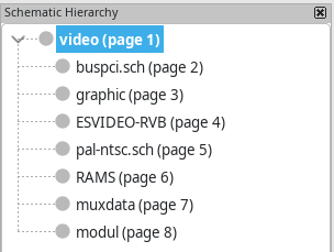
原理图之间的电气连接
原理图之间的电气连接是通过 标签进行的。在 KiCad 中,有几种标签,每种都有不同的连接范围。
-
Local labels only make connections within a sheet. Therefore local labels cannot be used to connect between sheets. Local labels are added with the
button. -
Global labels make connections anywhere in a schematic, regardless of sheet. Therefore global labels can be used to make connections between sheets whether the sheets are top-level or hierarchical. Global labels are added with the
button. -
Hierarchical labels in a hierarchical subsheet connect to hierarchical sheet pins accessible in the parent sheet. Hierarchical designs rely on hierarchical labels and pins to make connections between parent sheets and child sheets. You can think of sheet pins as defining the interface for a subsheet; hierarchical labels within the child sheet connect to corresponding sheet pins which are visible in the parent sheet. Hierarchical labels are added inside a child sheet using the
button.
| 如果在同一个原理图页面,无论标签类型如何,具有相同名称的标签将被连接。 |
| 隐藏电源引脚也可以被认为是全局标签,因为它们可以连接到原理图层次结构中的任何地方。 |
层次原理图引脚
After placing hierarchical labels within a subsheet, matching hierarchical sheet pins can be added to the subsheet symbol in the parent sheet. You can then make connections to the hierarchical pins with wires, labels, and buses. Hierarchical sheet pins in a subsheet symbol are connected to the matching hierarchical labels in the subsheet itself.
| 在原理图页面符中导入相应的层次原理图引脚之前,必须先在子原理图中定义层次化标签。 |
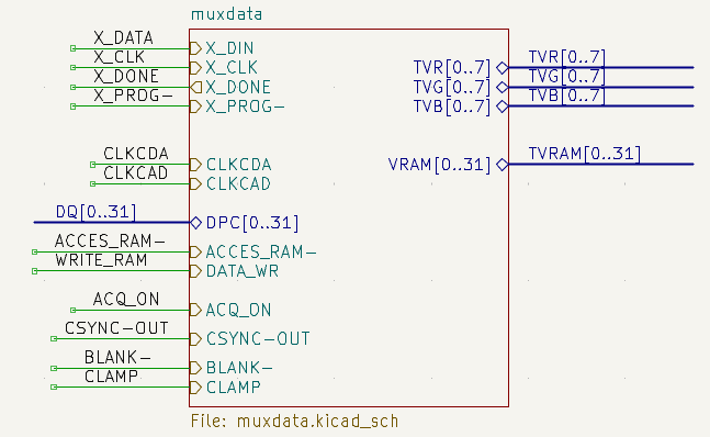
For every hierarchical label in the subsheet, add the corresponding hierarchical pin onto the sheet symbol by clicking the ![]() button in the right toolbar, then clicking on the sheet symbol. A sheet pin for the first unmatched hierarchical label will be attached to the cursor, where it can be placed anywhere along the border of the sheet symbol. Clicking again with the tool will continue to add additional sheet pins until all of the hierarchical labels in the subsheet have a matching sheet pin on the sheet symbol. Sheet pins can also be imported by selecting Place Sheet Pin in a sheet symbol’s right-click context menu.
button in the right toolbar, then clicking on the sheet symbol. A sheet pin for the first unmatched hierarchical label will be attached to the cursor, where it can be placed anywhere along the border of the sheet symbol. Clicking again with the tool will continue to add additional sheet pins until all of the hierarchical labels in the subsheet have a matching sheet pin on the sheet symbol. Sheet pins can also be imported by selecting Place Sheet Pin in a sheet symbol’s right-click context menu.
你可以在原理图页面引脚属性对话框中编辑页面引脚的属性。 通过双击原理图页面引脚,或选择页面引脚并使用快捷键 E ,或者右击原理图页面引脚并选择 属性… 来打开这个对话框。
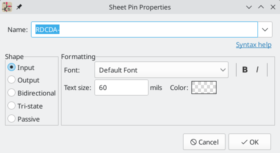
The sheet pin’s name can be edited in the textbox or by selecting from the dropdown list of hierarchical labels in the subsheet. A sheet pin’s name has to match the corresponding hierarchical label in the subsheet, so if you change a pin name you must change the label name as well.
Shape changes the shape of the sheet pin, and has no electrical effect. It can be set to Input, Output, Bidirectional, Tri-state, or Passive. The pin’s font, text size, color, and emphasis (bold or italic) can also be changed.
Syncing sheet pins
Another way to manage the connections between hierarchical labels and sheet pins is to use the Sync Sheet Pins tool. Launch this tool using the ![]() button in the right toolbar or with Sync Sheet Pins in a sheet symbol’s right click context menu.
button in the right toolbar or with Sync Sheet Pins in a sheet symbol’s right click context menu.
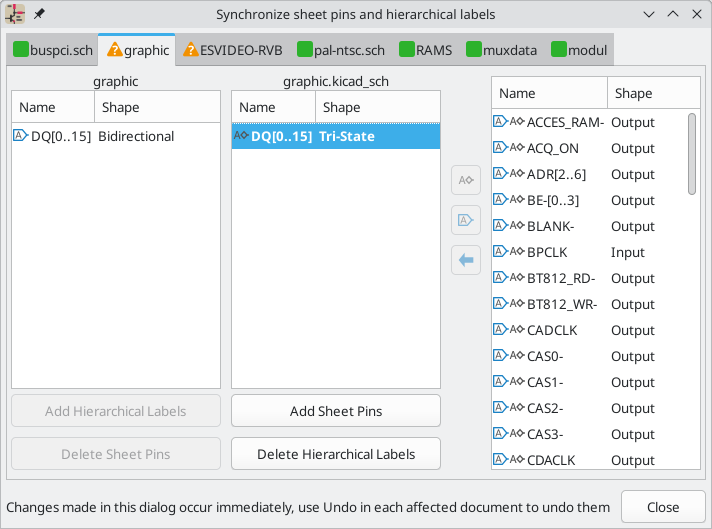
This dialog shows the hierarchical labels and hierarchical sheet pins for each hierarchical sheet. If the tool was launched from the context menu of a sheet symbol, only one tab will be available, with the labels and sheet pins for that specific sheet. If the tool was started globally, i.e. with the ![]() button or with Place → Sync Sheet Pins, a tab will be shown for each hierarchical sheet. If a sheet was selected in the editing canvas when the tool was launched, the dialog will open to that sheet’s tab.
button or with Place → Sync Sheet Pins, a tab will be shown for each hierarchical sheet. If a sheet was selected in the editing canvas when the tool was launched, the dialog will open to that sheet’s tab.
The icon in each tab indicates whether the hierarchical sheet pins on the sheet symbol are correctly matched with the hierarchical labels inside the sheet. If the tab has a ![]() icon, then there is a hierarchical label in the sheet without a matching sheet pin, or a sheet pin without a corresponding hierarchical label, or both. If the tab has a
icon, then there is a hierarchical label in the sheet without a matching sheet pin, or a sheet pin without a corresponding hierarchical label, or both. If the tab has a ![]() icon, then the hierarchical labels and hierarchical sheet pins are matched up correctly. Sheet pins and labels are considered matching if they have the same name and the same graphic shape (input, output, bidirectional, tri-state, or passive).
icon, then the hierarchical labels and hierarchical sheet pins are matched up correctly. Sheet pins and labels are considered matching if they have the same name and the same graphic shape (input, output, bidirectional, tri-state, or passive).
The column on the left lists sheet pins for the current sheet that do not have a corresponding hierarchical label in the sheet. The middle column lists hierarchical labels in the current sheet that do not have a corresponding hierarchical sheet pin on the sheet symbol. The right column lists pairs of matching sheet pins and hierarchical labels. The name of each pin or label is shown along with its graphic shape.
If you click the Add Hierarchical Labels button, new hierarchical labels corresponding to the selected sheet pins will be created for you to place sequentially in the sheet. The selected sheet pins are then removed from the left column and added to to the right column for matching sheet pins and labels. Clicking Delete Sheet Pins will delete the selected sheet pins from the sheet symbol.
If you click the Add Sheet Pins button, new sheet pins corresponding to the selected hierarchical labels will be created for you to place on the sheet symbol. The hierarchical labels are then removed from the middle column and added to the right column for matching sheet pins and labels. Clicking Delete Hierarchical Labels will delete the selected hierarchical labels from inside the sheet.
Clicking the ![]() button will match the selected sheet pin and hierarchical label by renaming the sheet pin to match the hierarchical label’s name. Clicking the
button will match the selected sheet pin and hierarchical label by renaming the sheet pin to match the hierarchical label’s name. Clicking the ![]() button will do the opposite, matching the selected sheet pin and hierarchical label by renaming the label to match the sheet pin.
button will do the opposite, matching the selected sheet pin and hierarchical label by renaming the label to match the sheet pin.
Clicking the ![]() button will unmatch a matched pair, moving both the sheet pin and the hierarchical label back to their respective unmatched columns. The unmatched sheet pin and hierarchical label can then be edited or rematched as desired.
button will unmatch a matched pair, moving both the sheet pin and the hierarchical label back to their respective unmatched columns. The unmatched sheet pin and hierarchical label can then be edited or rematched as desired.
Any changes made in the Sync Sheet Pins dialog are applied immediately, before the dialog is closed. To cancel a change made in the Sync Sheet Pins dialog, use Undo.
Multipage and hierarchical design examples
Multipage schematics in KiCad can be arranged in several ways. Which schematic organization is most appropriate depends on the design.
A design that conceptually contains nested blocks lends itself well to a hierarchical organization, especially if some of the blocks are repeated, because each block can be represented as a hierarchical subsheet. On the other hand, designs that conceptually don’t contain a hierarchy might be better represented using top-level sheets. You can also both strategies in the same schematic, using multiple top-level sheets while also using hierarchical subsheets.
Some examples of different schematic organizations are shown below.
Flat schematics
Flat schematics contain multiple top-level sheets; each top-level sheet follows the previous sheet, and all top-level sheets are at the same level of the hierarchy. None of the top-level sheets are nested under another sheet.
In the example below there are three top-level sheets, each with a name and a page number. They are not hierarchically nested, so hierarchical connections with hierarchical labels and sheet pins are impossible. Any net connections between sheets must be made with global labels (and global power symbols).
层次原理图
An example of a hierarchical design is the video demo project included with KiCad. The root sheet contains seven unique subsheets, each with hierarchical labels and sheet pins linking the sheets to each other in the root sheet. Each of the seven subsheets is used once; none are reused (see the next section for an example of reusing subsheets). Two of the subsheet symbols are shown below.
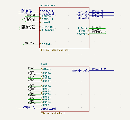
The subsheets are drawn as sheet symbols in the root sheet, meaning they are placed under the root sheet in the schematic hierarchy.
Reusing hierarchical subsheets
The multichannel demo project is an example of using a subsheet multiple times. The root sheet contains four subsheet symbols, which both refer to the same sheet file (channel_strip.kicad_sch). This allows the design to include four copies of the same audio mixer channel circuit. Although the four sheet symbols all refer to the same filename, the sheet names are unique (CH1, CH2, CH3, and CH4). Inside each subsheet the circuits are identical except for the reference designators, which as always are unique. The subsheets each have a single hierarchical label/pin connection to the root sheet, which contains the summing amplifier circuit that combines the output of each channel.
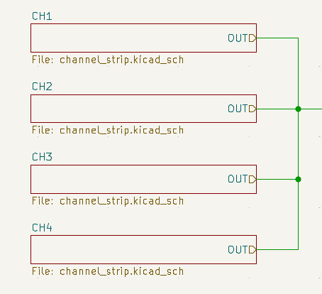
The subsheets are drawn as sheet symbols in the root sheet, meaning they are placed under the root sheet in the schematic hierarchy.
检查原理图
查找工具
查找工具在原理图中搜索文本,包括位号、引脚名称、符号字段和图形文本。当该工具找到一个匹配的文本时,画布会被放大并居中显示该匹配的文本。使用顶部工具栏上的 ![]() 按钮启动该工具。
按钮启动该工具。
查找工具有几个选项:
-
Match case: Selects whether the search is case-sensitive.
-
Whole words only: When selected, the search will only match the search term with complete words in the schematic. When unselected, the search will match if the search term is part of a larger word in the schematic.
-
Regular Expression: When selected, regular expressions can be used in the search terms.
-
Search pin names and numbers: Selects whether the search should apply to pin names and numbers.
-
Search net names: Selects whether the search should apply to net names (labels, symbol pins, sheet pins, and bus members).
-
Include hidden fields: Selects whether the search should apply only to visible fields or if it should include hidden symbol fields.
-
Search the current sheet only: Selects whether the search should be limited to the current schematic sheet.
-
Search the current selection only: Selects whether the search should be limited to the current selection.
还有一个查找和替换工具,可以通过顶部工具栏上的 ![]() 按钮激活。这个工具的作用与查找工具相同,但还可以用不同的文本替换部分或全部匹配的文本。
按钮激活。这个工具的作用与查找工具相同,但还可以用不同的文本替换部分或全部匹配的文本。
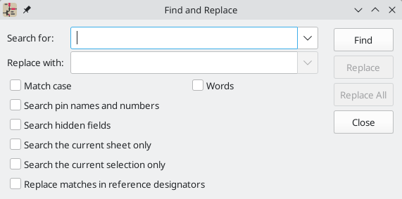
The Find and Replace tool has the same options as the Find tool, with one addition:
-
Replace matches in reference designators: When selected, reference designators will be modified if they contain matching text. Otherwise reference designators will not be affected.
Search panel
The search panel is a docked panel that lists information about symbols, text, labels, and groups from the schematic. Show or hide the search panel with View → Panels → Search or use the Ctrl+G shortcut.
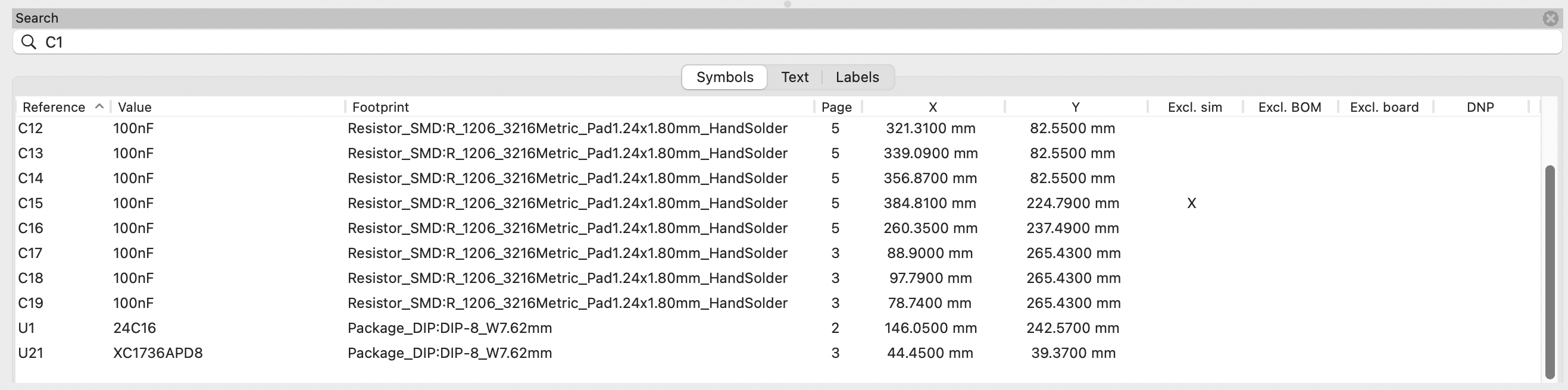
You can optionally filter the list based on a search string. When no filter is used, all items in the design are listed in the corresponding tab. Items from the entire schematic are listed, not just items in the current sheet. Items are filtered based on their properties:
-
Symbols and power symbols are filtered by the contents of their fields. You can select whether to search hidden fields by enabling the Search Hidden Fields option in the
 menu. Symbols are also filtered by their metadata (library link, description, and keywords) if Search Metadata is enabled in the menu.
 -
Text (text and textboxes) is filtered by the text content.
-
Labels are filtered by their netnames.
-
Groups are filtered by the group name.
You can sort the filtered results in ascending or descending order of the value in a particular column by clicking on that column header.
过滤器支持通配符:* 匹配任何字符,? 匹配任何单个字符。您还可以使用 正则表达式,如 /符号值/。
The displayed information depends on the item type:
-
All items list their name and/or value, page number, and X/Y location in the sheet as applicable.
-
Symbols additionally list their reference designator, footprint, attributes (Exclude from Simulation, Exclude from BOM, Exclude from Board, and Do Not Populate), library link (library name and symbol name), and description.
-
Power symbols additionally list their reference designator.
-
Text and labels additionally list their type, e.g. textbox or hierarchical.
When you click an item in the search panel, the schematic editor switches to the item’s schematic sheet, and the item is selected in the editing canvas. Depending on what is configured in the ![]() menu, the schematic editor will also pan and/or zoom to the selected item in the editing canvas. Double-clicking an item in the search panel opens its properties dialog.
menu, the schematic editor will also pan and/or zoom to the selected item in the editing canvas. Double-clicking an item in the search panel opens its properties dialog.
网络高亮显示
在原理图编辑器中,电气网络可以在原理图中所有出现的位置高亮显示。网络高亮显示可以在原理图编辑器中激活,也可以在启用交叉探测高亮时在 PCB 编辑器中高亮相应的网络是激活(见下文)。当网络高亮显示激活时,高亮的网络将以不同的颜色显示。默认情况下,这种颜色是粉红色,但可以在 "偏好设置" 对话框的颜色部分进行配置。
可以通过点击右边工具栏中的高亮显示网络工具(![]() )高亮显示网络。另外,高亮网络的快捷键(`)也可以高亮显示光标下的网络。
)高亮显示网络。另外,高亮网络的快捷键(`)也可以高亮显示光标下的网络。
可以使用清除网络高亮操作(快捷键 ~)或在原理图中的空白区域使用网络高亮显示工具来清除网络高亮网络。 默认情况下,Esc 也可以清除网络高亮显示,但如果需要,可以在 首选项 → 原理图编辑器 → 编辑选项 中将其禁用。
Net navigator
The net navigator is a docked panel that shows the location of every occurrence of a highlighted net in a schematic. Show or hide the net navigator with View → Panels → Net Navigator.
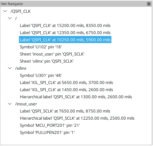
当您高亮显示原理图中的一个网络时,该网络在原理图中显示的每个位置都会在网络导航面板中列出。与该网络连接的所有标签、符号引脚和工作表引脚都会列出。每个出现点都在其原理图工作表下排序。单击一个出现点可在编辑画布中显示该项目。
When no net is highlighted, the net navigator displays this information for all nets in the schematic.
| The net navigator displays highlighted nets, not selected nets. |
You can filter the displayed nets by typing part of a net name in the Filter nets textbox. If Wildcard Search is enabled in the ![]() menu, you can use wildcards in the filter string:
menu, you can use wildcards in the filter string: * matches any characters, and ? matches any single character. If Regex Search is enabled instead, you can use regular expressions.
With the net navigator open and a net highlighted, you can quickly select various items on that net (net labels, sheet pins, and symbol pins) by selecting one of the items on the highlighted net in the schematic canvas and pressing Tab/Shift+Tab to cycle through the net items. Pressing Tab selects the next item on the net, while Shift+Tab selects the previous item.
从 PCB 上交叉探测
KiCad 允许在原理图和 PCB 之间进行双向交叉探测。 有几种不同类型的交叉探测。
Selection cross-probing allows you to select a symbol or pin in the schematic to select the corresponding footprint or pad in the PCB (if one exists) and vice-versa.
Cross-probing also works in the 3D Viewer. When a component is selected in the 3D Viewer, it is also selected in the schematic and PCB, and when a component is selected in the schematic or PCB, it is also selected in the 3D Viewer.
By default, cross-probing will result in the display centering on the cross-probed item and zooming to fit. You can disable the centering and zooming behavior, or disable selection cross-probing entirely, in the Display Options section of the Preferences dialog. When the Flash cross-probed selection setting is enabled, selection cross probing will cause the cross-probed item to flash three times, making it easier to spot.
Even when selection cross-probing is disabled, you can manually cross-probe from the schematic to the PCB by right-clicking an object and selecting Select on PCB, or from the PCB to the schematic by right-clicking an object and choosing Select → Select on Schematic.
Highlight cross-probing allows you to highlight a net in the schematic and PCB at the same time. If the option "Highlight cross-probed nets" is enabled in the Display Options section of the Preferences dialog, highlighting a net or bus in the schematic editor will cause the corresponding net or nets to be highlighted in the PCB editor, and vice versa.
Electrical rules checking
The Electrical Rules Checker (ERC) tool checks for certain errors in your schematic, such as unconnected pins, unconnected hierarchical symbols, shorted outputs or other illegal connections, etc. ERC violations are reported as errors or warnings depending on the severity of the issue detected.
ERC does not detect all errors, but it can detect many common issues and oversights. All detected issues should be checked and addressed before proceeding. The quality of the ERC is directly related to the care taken in declaring electrical pin properties during symbol creation. If symbols are designed incorrectly, ERC will not report accurate information.
ERC 可以通过点击顶部工具栏的 ![]() 按钮并点击 运行 ERC 按钮来启动。
按钮并点击 运行 ERC 按钮来启动。
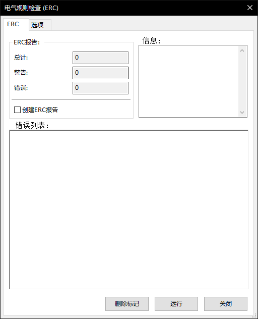
Any warnings or errors are reported in the Violations tab, and markers for each violation are placed in the schematic so that they point to the relevant part of the schematic. Warnings are indicated by yellow arrows, and errors have red arrows. Excluded violations are shown as green arrows. A list of the ignored tests are shown in the Ignored Tests tab. A report file in plain text format can be created after running DRC using the Save… button.
|
Selecting a violation in the ERC window jumps to the selected violation
marker in the schematic, according to the settings in the |
Certain types of violations have contextual actions in the context menu. For example, unannotated symbol violations have an action to run the annotation tool on the violating items. For schematic vs. library symbol mismatch violations, there is an action to run the Compare Symbol with Library tool and another action to update the symbol from the library. These actions can help to quickly fix or identify the reason for a particular violation.
The numbers at the bottom of the window show the number of errors, warnings, and exclusions. Each type of violation can be filtered from the list using the respective checkboxes. Clicking Delete Marker will clear the selected violation until ERC is run again, while clicking Delete All Markers will clear all violations until the next ERC run.
可以在对话框中右键点击违规行为,以忽略它们或改变其严重程度:
-
Exclude this violation: ignores this particular violation, but does not affect any other violations. You can un-exclude a violation by right clicking the excluded violation and selecting Remove exclusion for this violation.
-
Exclude with comment…: the same as Exclude this violation, but prompts for a comment explaining the reason for the exclusion. When excluded violations are unhidden (using the Exclusions checkbox), exclusion comments are shown with the corresponding excluded violation. To edit an existing exclusion comment or add a comment to an existing exclusion, right click an excluded violation and select Edit exclusion comment….
-
Change severity: changes a type of violation from warning to error, or error to warning. This affects all violations of a given type.
-
Ignore all: ignores all violations of a given type. This test will now appear in the Ignored Tests tab rather than the Violations tab. You can un-ignore the test again by right clicking the test in the Ignored Tests tab, or in the Violation Severity panel in Schematic Setup.
-
Edit violation severities…: opens the Violation Severity panel in Schematic Setup, for editing the severities of all DRC violation types.
你也可以用 检查 → 排除标记 排除所选标记,用 查看 菜单显示或隐藏每一类标记(错误、警告和排除)。
Excluded and ignored violations are remembered between runs of the design rule checker. Excluded violations are hidden unless the Exclusions checkbox is enabled. Ignored violations are not shown, but there is a list of ignored tests in the Ignored Tests tab.
ERC 例子
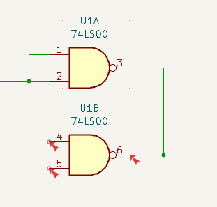
在上面的截图中,有三个错误。
-
两个输出被连接在一起(右边的红色箭头)。
-
有两个输入没有连接(左边的红色箭头)。实际上每个引脚都有两个错误:引脚未连接,而且每个引脚都是没有被输出引脚驱动的输入引脚。
选择一个 ERC 标记会在窗口底部的信息窗格中显示违规描述。
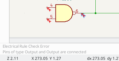
Per-net ERC markers
Some violations are reported only once per net. For example, the "Input Power pin not driven by any Output Power pins" error technically applies to each Input Power pin on an un-driven net, but only one marker is shown per net. This is to avoid producing a large number of markers for a single root cause. In this case, exactly where the marker is placed in the schematic is arbitrary and does not necessarily indicate the ideal location for fixing the issue.
|
All errors for a given net will be reported when the Show all errors option is enabled in the |
In the example below, there are four un-driven Input Power pins (one per power symbol), but only two ERC markers. Adding two PWR_FLAG symbols, one to each un-driven net, will clear the errors. The "correct" location for the PWR_FLAG symbol depends on the schematic and may not be near the particular power symbol where the marker was placed, or even in the same schematic sheet.
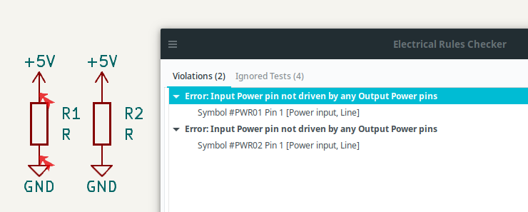
电源引脚和电源标志
如下面的例子所示,在电源引脚上出现 "输入电源引脚未被任何输出电源引脚驱动" 的错误是很常见的,即使电源引脚似乎正确地连接到电源导线。这种情况发生在通过连接器或其他没有被标记为电源输出的元件提供电源的设计中。在这些情况下,ERC 不会检测到任何连接到网络的输出电源引脚,而会判断输入电源引脚没有被电源驱动。
For example, in the below schematic, VCC and GND are connected to a connector with passive pins, so the Input Power pins of U1 are not considered driven by a power source.
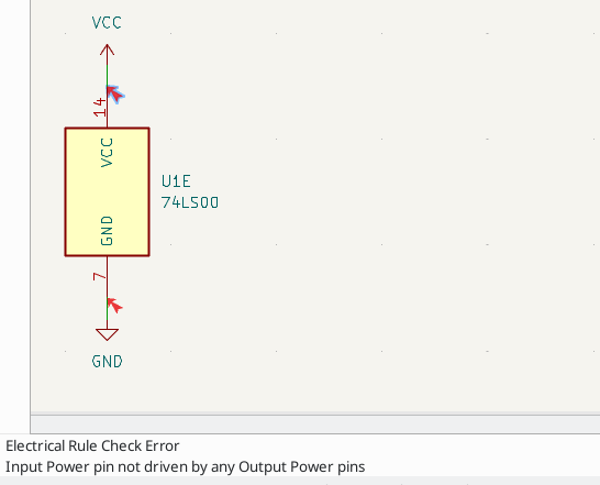
To avoid this warning, connect the net to PWR_FLAG symbol on such a power net as shown in the following example. The PWR_FLAG symbol is found in the power symbol library. Alternatively, connect any Output Power pin to the net; PWR_FLAG is simply a symbol with a single Output Power pin.
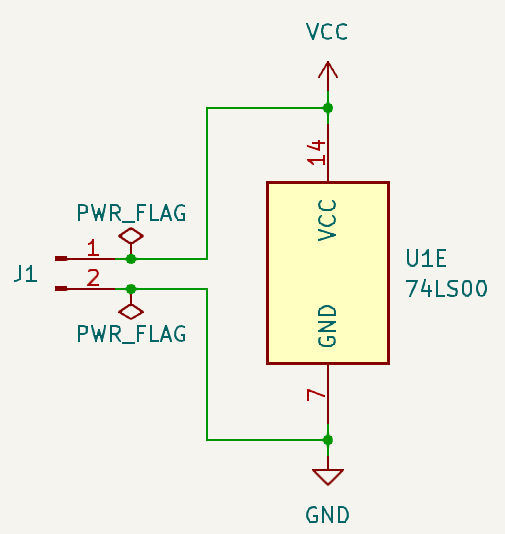
Ground nets often need a PWR_FLAG to be manually added, even when power rails do not, because voltage regulators have outputs declared as Output Power, but their ground pins are typically marked as Power Inputs. Therefore grounds are not considered driven by these voltage regulators. This is so multiple regulators can share a common ground without errors caused by two Output Power pins being connected together.
Power nets do not "jump" across components, so, components like passive inline filtering elements may need a PWR_FLAG on their downstream side to indicate that the net is still connected to a power source.
In the below schematic, although there is a PWR_FLAG on the nets connected to the connectors (VCC_IN and GND_IN), a PWR_FLAG is also needed to mark each of VCC and GND as power nets, because the filter FL1 has only Passive pins.
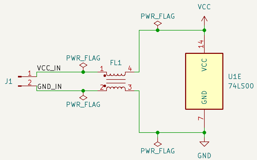
This would be the case also if the VCC_IN and GND_IN nets were connected to a symbol with Output Power pins. In fact, in this schematic, the PWR_FLAG symbols are on VCC_IN and GND_IN are not required, as there are no Input Power pins on those nets.
关于电源引脚和电源标志的更多信息,请参见PWR_FLAG 文档。
ERC 配置
原理图设置中的 违规严重性 面板让你配置哪些类型的 ERC 应被报告为错误、警告或忽略。
原理图设置中的 引脚冲突映射 面板允许你配置连接规则,根据哪些类型的引脚相互连接来定义错误和警告的电气条件。例如,默认情况下,当一个输出引脚与另一个输出引脚连接时,会产生错误。
可以通过点击矩阵中的方块来改变规则,使其在各种选择中循环:允许、警告、错误。
ERC 检查清单
下表列出了 KiCad 检查的电气规则和每个检查的默认违规严重程度。所有严重程度都是可配置的。
Connections ERC checks
These ERC checks look for issues with wire and label connections in the schematic.
| Violation | 描述 | Default Severity |
|---|---|---|
Pin not connected |
This violation occurs when a symbol pin is not connected to a net, unless the pin has a no-connect flag or has electrical type Unconnected. |
错误 |
Input pin not driven by any Output pins |
This violation occurs when a symbol pin with electrical type Input is not connected to a driving pin. Driving pins are pins with the type output, bidirectional, tristate, power output, or passive pins. |
错误 |
Input Power pin not driven by any Output Power pins |
This violation occurs when a symbol pin with electrical type Input Power is not connected to an Output Power pin. A common cause of this violation is described above. |
错误 |
A pin with a "no connection" flag is connected |
The violation occurs when a symbol pin with a no connection flag is connected to a net. |
警告 |
Unconnected "no connection" flag |
This violation occurs when a No connection flag is not connected to a pin or label. |
警告 |
Label not connected |
This violation occurs when a global, hierarchical, local, or directive label is not connected to a pin or another label. |
错误 |
Label connected to only one pin |
This violation occurs when a label is connected to a net with fewer than two symbol pins on it. This indicates the label isn’t being used to connect anything, as it it is only connected to a single symbol pin. |
警告 |
Global label only appears once in the schematic |
This violation occurs when a global label only appears once in the schematic, meaning that the label is not forming any global connections. This violation is ignored by default to allow users to use global labels to label nets, even if the net does not connect anywhere else. |
Ignore |
Local and global labels have the same name |
This violation occurs when a local label has the same name as a global label. If these labels are on separate sheets, they will not connect, although they may have been intended to connect. Note that while a local label and a global label with the same name won’t connect if they are on different sheets, they will connect if they are on the same sheet. |
警告 |
Local and global power symbols have the same name |
This violation occurs when a local power symbol has the same name as a global symbol. If these power symbols are on separate sheets, they will not connect, although they may have been intended to connect. Note that while a local symbol and a global power symbol with the same name won’t connect if they are on different sheets, they will connect if they are on the same sheet. |
警告 |
Wires not connected to anything |
This violation occurs when a wire is not connected to any pin or label. |
错误 |
Bus Entry needed |
This violation only applies to projects imported from EAGLE projects. It indicates places where the importer was unable to automatically add bus entries to the imported schematic, so you must add them by hand. |
错误 |
Symbol pin or wire end off connection grid |
This violation occurs when a symbol pin or wire end is not aligned to the connection grid. Symbol pins and wire ends need to be aligned to the grid in order to connect to each other. The grid used for this check is defined by the connection grid setting in Schematic Setup → Formatting → Connection grid. |
警告 |
Four connection points are joined together |
This violation occurs when wires join in a four-way (cross) junction. Such junctions are sometimes considered harmful because it can be unclear if all four wires are intended to be joined or if two wires were intended to cross without a junction. |
Ignore |
Duplicate pins with different nets |
This violation occurs when two pins in the same symbol have the same pin number but are connected to different nets. Symbol pins do not need to be uniquely numbered within a symbol, but all pins with the same pin number need to be connected to the same net. This violation is always an error. |
Error (not configurable) |
Label connects more than one wire |
This violation occurs when a label anchor connects to two wires (where two wires cross without connecting). In this situation is not possible to determine which net the label should connect to. |
警告 |
Unconnected wire endpoint |
This violation occurs when a wire endpoint is not connected to anything. |
警告 |
Conflicts ERC checks
These ERC checks look for conflicting information in symbols, sheets, and buses.
| Violation | 描述 | Default Severity |
|---|---|---|
Duplicate reference designators |
This violation occurs when two symbols have the same reference designator. |
错误 |
Units of same symbol have different values |
This violation occurs when units of a single symbol have different values. |
错误 |
Different footprint assigned in another unit of the symbol |
This violation occurs when units of a single symbol have different assigned footprints. |
错误 |
Different net assigned to a shared pin in another unit of the symbol |
This violation occurs when a pin that is shared between multiple units of a symbol is not connected to the same net in each unit. |
错误 |
Duplicate sheet names within a given sheet |
This violation occurs when two hierarchical sheets in the same parent sheet have the same name. |
错误 |
Mismatch between hierarchical labels and sheet pins |
This violation occurs when a hierarchical label does not have a corresponding hierarchical sheet pin in the parent sheet, or a hierarchical sheet pin does not have a corresponding hierarchical label in the child sheet. |
错误 |
More than one name given given to this bus or net |
This violation occurs when a net has multiple labels attached. Nets can only have a single name, so if multiple labels are attached to a net, one name will be selected and used as the canonical name. |
警告 |
Conflict between bus alias definitions across schematic sheets |
This violation occurs when a bus alias has different members in different sheets. If the same bus alias name is used in multiple sheets, the members of the alias must be the same for each sheet. |
错误 |
Buses are graphically connected but share no bus members |
This violation occurs when buses that are graphically connected do not have bus members in common. |
错误 |
Invalid connection between bus and net items |
This violation occurs when a bus is connected to a net item, such as a wire, a label referring to a single net, or a sheet pin referring to a single net. Labels and sheet pins can only be connected to buses if they refer to buses rather than individual signals. |
错误 |
Net is graphically connected to a bus but not a bus member |
This violation occurs when a net is connected to a bus with a bus entry but the net is not a member of that bus. |
警告 |
Ground pin not connected to ground net |
This violation occurs when a power input or power output pin with a name containing "GND" is connected to a net with a name that doesn’t contain "GND", but another power pin in the same symbol is connected to a "GND" net. This indicates that the GND pin is likely misconnected. The comparison is case-insensitive, so "GND", "gnd", and any other combination of uppercase and lowercase letters are all considered GND pins/nets. |
警告 |
Miscellaneous ERC checks
These ERC checks look for other miscellaneous issues in the schematic.
| Violation | 描述 | Default Severity |
|---|---|---|
Pin name resembles stacked pin |
This violation occurs when a symbol’s pin number resembles a stacked pin range but is malformed or invalid, and therefore the pin is not treated as a stacked pin. |
警告 |
Field name has leading or trailing whitespace |
This violation occurs when a symbol or sheet field starts or ends wth whitespace. Leading or trailing whitespace isn’t necessarily a problem, but it can be undesired and hard to notice. |
警告 |
Symbol is not annotated |
This violation occurs when a symbol is not annotated with a unique reference designator. |
错误 |
Unresolved text variable |
This violation occurs when a text variable ( |
错误 |
Undefined netclass |
This violation occurs when a netclass is assigned graphically
(i.e. in the |
错误 |
SPICE model issue |
This violation occurs when a SPICE model has a syntax error or other problem. |
Ignore |
Labels are similar (lower/upper case difference only) |
This violation occurs when two labels are similar and differ only by the case of some letters. This may be a typo causing two labels to be disconnected when they are intended to be connected. |
警告 |
Power pins are similar (lower/upper case difference only) |
This violation occurs when the net names driven by two global power pins are similar and differ only by the case of some letters. This may be a typo causing two global power pins to be disconnected when they are intended to be connected. |
警告 |
Power pin and label are similar (lower/upper case difference only) |
This violation occurs when a label and the net name driven by a global power pin are similar and differ only by the case of some letters. This may be a typo causing two global power pins to be disconnected when they are intended to be connected. |
警告 |
Library symbol issue |
This violation occurs when one of several symbol library issues is detected:
|
警告 |
Symbol doesn’t match copy in library |
This violation occurs when a symbol in the schematic is different than the library version of the symbol. You can compare between the schematic and library versions of the symbol using the Compare Symbol with Library tool, which is available by right clicking the violation in the ERC window. If desired, you can update the schematic symbol to match the library symbol. |
警告 |
Footprint link issue |
This violation occurs when one of several footprint assignment issues is detected:
|
警告 |
Assigned footprint doesn’t match footprint filters |
This violation occurs when the footprint assigned to a symbol does not match the symbol’s footprint filters. If the symbol doesn’t have any footprint filters, no violation occurs. |
警告 |
Symbol has more units than are defined |
This violation occurs when a symbol has more units placed in the schematic than are defined in the symbol. Units in the schematic must correspond exactly to the symbol definition. |
错误 |
Symbol has units that are not placed |
This violation occurs when a unit from a multi-unit symbol is not placed in the schematic. Unplaced units will not be connected to anything. |
警告 |
Symbol has input pins that are not placed |
This violation occurs when a multi-unit symbol has units with input pins that are not placed, so those input pins will not be connected to anything. |
警告 |
Symbol has bidirectional pins that are not placed |
This violation occurs when a multi-unit symbol has units with bidirectional pins that are not placed, so those input pins will not be connected to anything. |
警告 |
Symbol has power input pins that are not placed |
This violation occurs when a multi-unit symbol has units with power input pins that are not placed, so those input pins will not be connected to anything. |
错误 |
Conflict problem between pins |
This violation occurs when a connection between pins is not allowed per the allowed connections in the Pin Conflicts Map. |
From Pin Conflicts Map |
User-definable ERC violations
You can manually trigger schematic ERC warnings or errors using special text variables. These items will appear as errors or warnings when ERC runs. This can be useful to flag items for later followup or review.
To cause an ERC violation, use the text variable ${ERC_ERROR <violation name>} or ${ERC_WARNING <violation name>} depending on whether an error or warning is desired. You can place this in a text item, text box, or field, including symbol fields, sheet fields, and label fields. When ERC runs, this will generate a ERC violation with the given violation name. These text variables resolve to an empty string in the schematic, and any text after the braces is included in the ERC violation’s description. The text variable must be placed at the start of the text object in order to trigger a violation.
For example, a text item containing ${ERC_ERROR TODO}Calculate resistor value will appear in the board as just the text "Calculate resistor value", and will generate an ERC error named "TODO" with "Calculate resistor value" in the description.
ERC 报告文件
An ERC report file can be generated and saved by clicking the Save… button in the ERC dialog. The file extension for ERC report files is .rpt.
ERC reports can also be generated by the kicad-cli tool in either text (.rpt) format or JSON.
|
分配封装
在对 PCB 进行布线之前,需要为每一个将要装配在电路板上的元件选择封装。封装定义了物理元件和电路板上的布线之间的铜连接。
有些符号预分配了封装,但对许多符号来说,有多种可能的封装,所以用户需要选择合适的封装。
KiCad 提供了几种分配封装的方法:
-
符号属性
-
符号属性对话框
-
符号字段表
-
-
在放置符号的同时
-
封装分配工具
下面将对每种方法进行解释。使用哪种方法是一个偏好的问题;根据情况,某种方法可能更方便。所有这些方法都是等效的,它们在符号的 封装 字段中存储所选封装的名称。
| 封装库表需要在分配封装之前进行配置。关于配置封装库表的信息, 请参见 PCB Editor manual。 |
在符号属性中分配封装
符号的 封装 字段可以直接在符号的属性窗口中编辑。
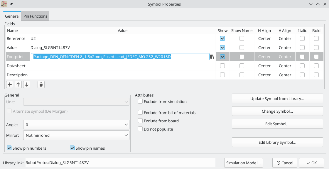
Clicking the ![]() button in the
button in the Footprint field opens the Footprint Chooser, which shows the available footprints sorted by footprint libraries.
The Footprint Chooser filters footprints by name, description, and keywords, as well as any fields that are shown as columns, according to what you type into the search field. * and ? wildcards are available. The footprint search behaves the same as in the symbol chooser dialog. You can choose to sort search results alphabetically or by best match using the options in the ![]() menu.
menu.
If the symbol defines any footprint filters, the apply footprint filters option can be used to hide footprints that don’t match those filters. If the filter by pin count option is selected, only footprints that match the symbol’s pincount will be listed.
Single clicking a footprint name selects the footprint, shows its name, description, and keywords in the bottom pane, and displays it in the preview pane on the right. Clicking the ![]() button shows or hides the description pane. You can show and hide 2D and 3D previews of the footprint by clicking the
button shows or hides the description pane. You can show and hide 2D and 3D previews of the footprint by clicking the ![]() and
and ![]() buttons (Show 3D viewer in own window causes the 3D preview to be opened in a new window).
buttons (Show 3D viewer in own window causes the 3D preview to be opened in a new window).
Double clicking on a footprint closes the chooser and sets the symbol’s Footprint field to the selected footprint.
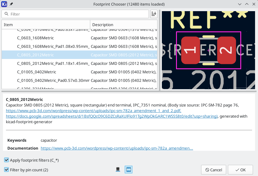
用符号字段表分配封装
和单独编辑每个符号的属性相比,符号字段表可以用来在一个地方查看和编辑设计中所有符号的属性。这包括通过编辑每个符号的 封装 字段来分配封装。
符号字段表可以通过 工具 → 编辑符号字段…,或者通过顶部工具栏上的 ![]() 按钮进入。
按钮进入。
`封装`字段在这里的作用与符号属性窗口的作用相同:可以直接编辑,也可以用封装库浏览器直观地选择封装。
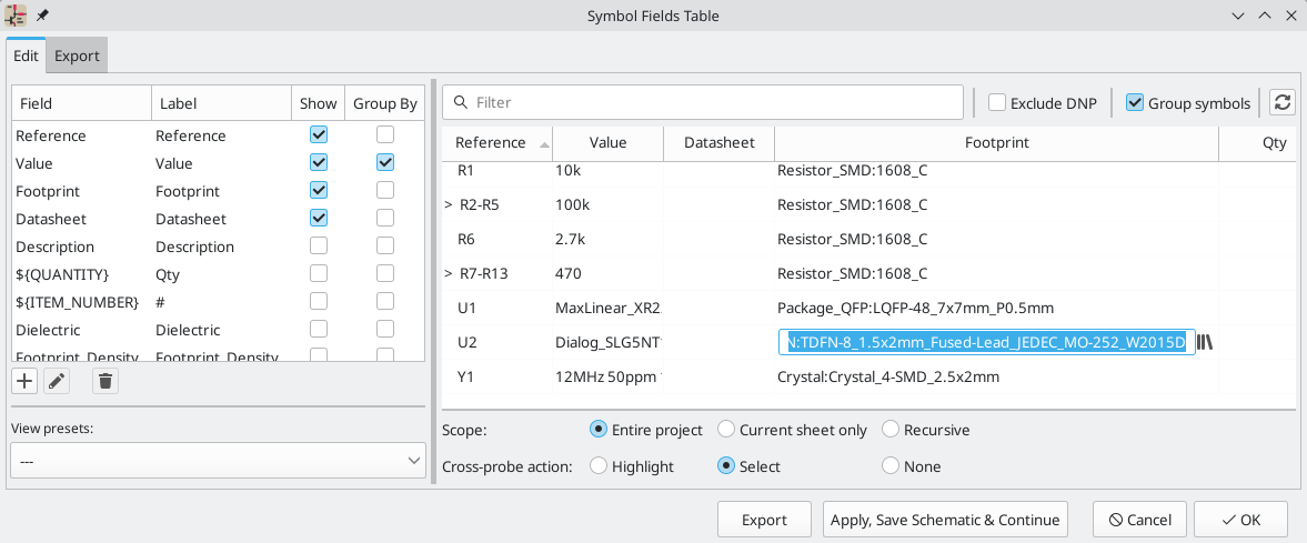
关于符号字段表的更多信息,请参见关于编辑符号属性章节。
放置符号时分配封装
当符号第一次被添加到原理图中时,可以为符号分配封装。
Some symbols are defined with a default footprint. These symbols will have this footprint preassigned when they are added to the schematic. If a symbol has a default footprint, the footprint will be graphically previewed in the symbol chooser dialog when the symbol is selected. For symbols without a default symbol defined, the footprint dropdown will say "No default footprint", and the footprint preview canvas will say "No footprint specified".
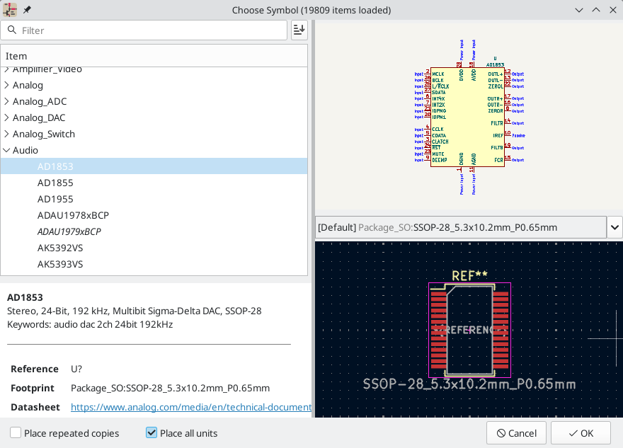
符号可以有封装过滤器,指定哪些封装适合与该符号一起使用。如果为选定的符号定义了封装过滤器,那么所有符合封装过滤器的封装都会作为选项出现在封装下拉菜单中。选定的封装将显示在预览画布中,当符号被添加到原理图中时,将被分配给该符号。
| 除非加载封装库,否则封装选项不会出现在封装下拉菜单中。在一个会话中第一次打开 "封装编辑器" 或 "封装库浏览器" 时,将加载封装库。 |
关于封装过滤器的更多信息,请参阅符号编辑器文档。
用封装分配工具分配封装
封装分配工具允许你将原理图中的符号与印制电路板布线时用到的封装关联起来。它提供了封装列表过滤、封装查看和3D元件模型查看,以确保将正确的封装与每个元件联系起来。
元件可以手动或通过创建等效文件(.equ 文件)自动分配到其相应的封装。等效文件是将每个元件与它的封装联系起来的查找表。
点击 工具 → 分配封装… 来运行该工具,或者点击顶部工具栏上的 ![]() 图标。
图标。
封装分配工具概述
下面的图片显示了封装分配工具的主窗口。
-
左边的窗格包含了与该工程相关的可用封装库的列表。
-
中间窗格包含原理图中的符号列表。
-
右边的窗格包含了从工程封装库加载的可用封装列表。
-
底部的窗格描述了应用于封装列表的过滤器,并打印了在最右边窗格中选择的封装的信息。
顶部的工具条包含以下命令:
|
Transfer the current footprint associations to the schematic. |
|
Edit the global and project footprint library tables. |
|
View the selected footprint in the footprint viewer. |
|
Select the previous symbol without a footprint association. |
|
Select the next symbol without a footprint association. |
|
Undo last edit. |
|
Redo last edit. |
|
Perform automatic footprint association using an equivalence file. |
|
Delete all footprint assignments. |
|
Filter footprint list by footprint filters defined in the selected symbol. |
|
Filter footprint list by pin count of the selected symbol. |
|
Filter footprint list by selected library. |
下表列出了封装分配工具的键盘命令:
Right Arrow / Tab |
Activate the pane to the right of the currently activated pane. Wrap around to the first pane if the last pane is currently activated. |
Left Arrow |
Activate the pane to the left of the currently activated pane. Wrap around to the last pane if the first pane is currently activated. |
Up Arrow |
Select the previous item of the currently selected list. |
Down Arrow |
Select the next item of the currently selected list. |
Page Up |
Select the item one full page upwards of the currently selected item. |
Page Down |
Select the item one full page downwards of the currently selected item. |
Home |
Select the first item of the currently selected list. |
End |
Select the last item of the currently selected list. |
使用 "封装分配工具" 手动分配 "封装"
要手动将一个封装与一个元件关联起来,首先在元件(中间)窗格中选择一个元件。然后在封装(右)窗格中选择一个封装,双击所需封装的名称。封装将被分配给选定的元件,而下一个没有分配封装的元件将被自动选择。
| 如果没有封装出现在封装窗格中,检查封装过滤选项是否正确应用。 |
当所有的元件都有封装时,点击 OK 按钮来保存分配并退出工具。或者,点击 取消,放弃更新的赋值,或者点击 应用,保存原理图并继续,保存新的赋值,而不退出工具。
筛选 "封装" 列表
有四个过滤选项可以限制哪些封装显示在封装窗格中。过滤选项是通过顶部工具栏的三个按钮和一个文本框来启用和禁用的。
-
 :激活 过滤器可以在每个符号中定义。 例如,一个运算放大器符号可以定义过滤器,只显示 SOIC 和 DIP 封装。
 -
 :只显示符合所选符号引脚数的封装。
 -
 :只显示左侧窗格中选择的库的封装。
 -
在文本框中输入文本,会隐藏与文本不匹配的封装。当文本框为空时,该过滤器被禁用。
当所有的过滤器被禁用时,会显示完整的封装列表。
窗口的底部窗格中描述了应用的过滤器,以及符合所选过滤器的封装数量。例如,当符号的封装过滤器和引脚数过滤器被启用时,底部窗格会打印封装过滤器和引脚数:
可以同时使用多个过滤器来帮助缩小封装窗格中可能合适的封装列表。KiCad 标准库中的符号定义了封装过滤器,旨在与引脚数过滤器结合使用。
使用封装分配工具自动分配封装
封装分配工具允许你在一个外部文件中存储封装分配,并在以后加载这些分配,甚至在不同的工程中。这使你能够自动将符号与适当的封装联系起来。
外部文件被称为等效文件,它存储了一个符号到相应的封装的映射。等效文件通常使用 .equ 文件扩展名。等效文件是具有简单语法的纯文本文件,必须由用户用文本编辑器来创建。语法描述如下。
你可以在 "封装分配工具" 中点击 偏好设置 → 管理 "封装关联文件" 来选择使用哪些等效文件。
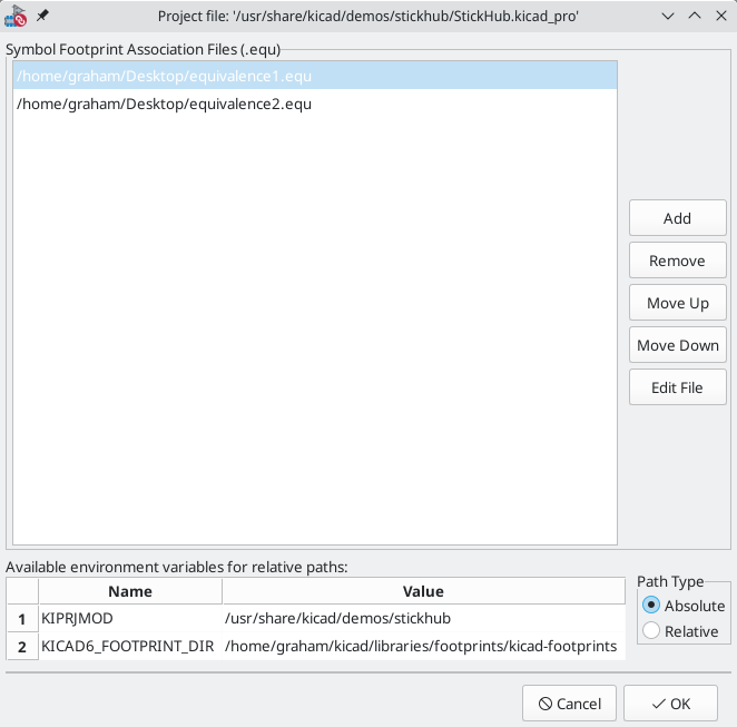
-
通过点击 添加 按钮添加新的等效文件。
-
点击 删除 按钮,删除所选的等效文件。
-
通过点击 上移 和 下移 按钮改变等效文件的优先级。如果一个符号的值在多个等效文件中被发现,最后一个匹配的等效文件的封装将覆盖早期的等效文件。
-
点击 编辑文件 按钮,打开所选的等效文件。
相关的环境变量显示在窗口的底部。当 相对 路径选项被选中时,这些环境变量将被自动用于使所选等效文件的路径与项目或封装库相对。
一旦所需的等效文件以正确的顺序载入,就可以通过点击封装分配工具顶部工具栏上的 ![]() 按钮来进行自动封装分配。
按钮来进行自动封装分配。
所有在加载的等效文件中找到的符号都将自动分配其封装。然而,已经分配了封装的符号将不会被更新。
等效文件格式
等效文件中每一行代表一个符号。每行都有以下结构:
'<symbol value>' '<footprint library>:<footprint name>'
每个名称/值必须用单引号(')包围,并由一个或多个空格隔开。以 # 开头的行是注释。
例如,如果你想让所有值为 LM4562 的符号被分配到 Package_SO:SOIC-8_3.9x4.9_P1.27mm 的封装,等效文件中的一行应该是:
'LM4562' 'Package_SO:SOIC-8_3.9x4.9_P1.27mm'
下面是一个等效文件的例子:
#integrated circuits (smd):
'74LV14' 'Package_SO:SOIC-14_3.9x8.7mm_P1.27mm'
'EL7242C' 'Package_SO:SOIC-8_3.9x4.9_P1.27mm'
'DS1302N' 'Package_SO:SOIC-8_3.9x4.9_P1.27mm'
'LM324N' 'Package_SO:SOIC-14_3.9x8.7mm_P1.27mm'
'LM358' 'Package_SO:SOIC-8_3.9x4.9_P1.27mm'
'LTC1878' 'Package_SO:MSOP-8_3x3mm_P0.65mm'
'24LC512I/SM' 'Package_SO:SOIC-8_3.9x4.9_P1.27mm'
'LM2903M' 'Package_SO:SOIC-8_3.9x4.9_P1.27mm'
'LT1129_SO8' 'Package_SO:SOIC-8_3.9x4.9_P1.27mm'
'LT1129CS8-3.3' 'Package_SO:SOIC-8_3.9x4.9_P1.27mm'
'LT1129CS8' 'Package_SO:SOIC-8_3.9x4.9_P1.27mm'
'LM358M' 'Package_SO:SOIC-8_3.9x4.9_P1.27mm'
'TL7702BID' 'Package_SO:SOIC-8_3.9x4.9_P1.27mm'
'TL7702BCD' 'Package_SO:SOIC-8_3.9x4.9_P1.27mm'
'U2270B' 'Package_SO:SOIC-16_3.9x9.9_P1.27mm'

#regulators
'LP2985LV' 'Package_TO_SOT_SMD:SOT-23-5_HandSoldering'
查看当前封装
封装分配工具包含一个封装查看器。点击顶部工具栏上的 ![]() 按钮可以启动封装查看器,并显示选定的封装。
按钮可以启动封装查看器,并显示选定的封装。
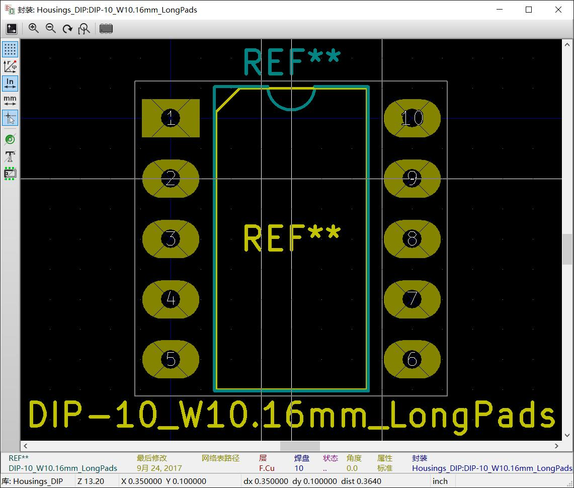
顶部的工具条包含以下命令:
|
Refresh view |
|
Zoom in |
|
Zoom out |
|
Zoom to fit drawing in display area |
|
Show 3D viewer |
左边的工具条包含以下命令:
|
Use the select tool |
|
Interactively measure between two points |
|
Display grid dots or lines |
|
Switch between polar and cartesian coordinate systems |
|
Use inches |
|
Display coordinates in mils (1/1000 of an inch) |
|
Display coordinates in millimeters |
|
Toggle display of full-window crosshairs |
|
Toggle between drawing pads in sketch or normal mode |
|
Toggle between drawing pads in normal mode or outline mode |
|
Toggle between drawing text in normal mode or outline mode |
|
Toggle between drawing graphic lines in normal mode or outline mode |

正向和反向批注
从原理图更新 PCB(正向批注)
使用 "从原理图更新 PCB" 工具将设计信息从原理图编辑器同步到电路板编辑器。在原理图编辑器和电路板编辑器中都可以用 工具 → 从原理图更新 PCB(F8)来访问该工具。你也可以使用电路板编辑器顶部工具栏上的 ![]() 图标。这个过程通常被称为正向批注。
图标。这个过程通常被称为正向批注。
| 从原理图更新 PCB 是将设计信息从原理图转移到 PCB 的首选方法。在旧版本的 KiCad 中,相应的过程是将网表从原理图编辑器中导出并导入到电路板编辑器中。现在已经没有必要使用网表文件了。 |
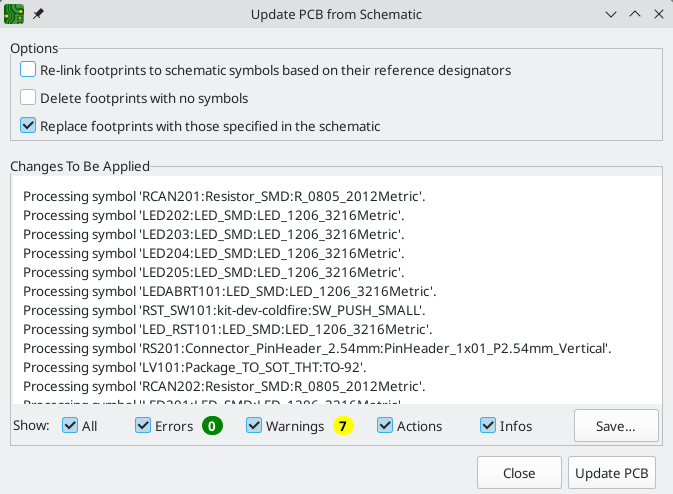
该工具将每个符号的封装添加到电路板上,并将更新的原理图信息传输到电路板上。同时,电路板的网络连接会被更新以匹配原理图。带有排除在电路板属性之外 的符号不会被更新到 PCB 上。
将对 PCB 进行的修改列在 待应用修改 窗格中。点击 更新 PCB 按钮之前,PCB 不会被修改。
你可以使用窗口底部的复选框来显示或隐藏不同类型的信息。可以使用 保存… 按钮将更改的报告保存到文件中。
选项
该工具有几个选项可以控制其行为。
| Option | 描述 |
|---|---|
Re-link footprints to schematic symbols based on their reference designators |
Footprints are normally linked to schematic symbols via a unique identifier created when the symbol is added to the schematic. A symbol’s unique identifier cannot be changed, but will be lost when the symbol is deleted, even if a symbol with the same reference designator replaces it. If checked, each footprint in the PCB will be re-linked such that each footprint has its unique identifier updated to match the symbol that has the same reference designator as the footprint. This option should generally be left unchecked. See below for more details on when to use this option. |
Group footprints based on symbol group |
If checked, footprints will be added to groups in the PCB if their linked symbols are grouped. |
Replace footprints with those specified by symbols |
If checked, footprints in the PCB will be replaced with the footprint that is specified in the corresponding schematic symbol. If unchecked, footprints that are already in the PCB will not be changed, even if the schematic symbol is updated to specify a different footprint. |
Delete footprints with no symbols |
If checked, any footprint in the PCB without a corresponding symbol in the schematic will be deleted from the PCB. Footprints with the "Not in schematic" attribute will be unaffected. If unchecked, footprints without a corresponding symbol will not be deleted. |
Override locks |
If checked, locking a footprint will not affect whether a footprint is deleted or replaced based on changes in the schematic. If unchecked, locked footprints will never be deleted or replaced even if they otherwise would be. |
Update footprint fields from symbols |
If checked, new and updated fields in symbols will be transferred to the corresponding footprints, keeping symbol and footprint fields in sync. If unchecked, footprint fields will not be updated when fields change in the corresponding symbols. |
Remove footprint fields not found in symbols |
If checked, footprint fields will be removed if they do not exist in the corresponding symbol. If unchecked, footprint fields that do not exist in the corresponding symbol will not be removed, allowing footprints to have additional fields compared to the corresponding symbols. |
Re-linking symbols and footprints
Symbols and footprints are linked together using unique identifiers (also called UUIDs). These are handled automatically within KiCad and are not usually visible to users. They allow a symbol and its partner footprint to keep their connection between schematic and PCB, even if the reference designator is changed. New objects get assigned their identifiers upon creation.
Re-linking by unique identifier (default)
In normal use, the Re-link footprints to schematic symbols based on their reference designators option should be unchecked. In this mode, symbols with the same identifier as a footprint will update that footprint, regardless of the reference designator. Symbols which have an identifier that doesn’t match any footprint will add a new footprint linked to that identifier.
For example, in the below schematic, both R1 and R2 are linked via their unique IDs to footprints on the PCB:
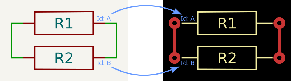
If symbol reference designators are changed in the schematic (e.g. by re-annotation), running the Update PCB from Schematic process will update the reference designators on the PCB.
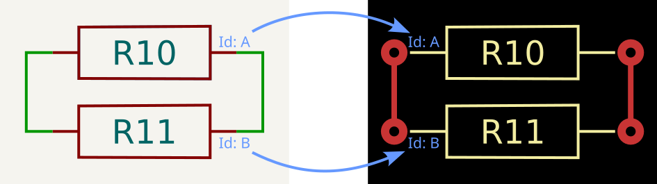
Re-linking by reference designator
If the checkbox is checked, the linking process is done using the reference designators. This can be useful for workflows that result in a symbol being deleted and replaced by another one, rather than being updated in-place. For example, cut-and-pasting a block of schematic or a sheet and copy-pasting and re-annotating will usually break the identifier-based links.
For example in the below case, the resistors R1 and R2 have been deleted and replaced, then re-annotated. While the reference designators are the same, the internal identifiers have changed. Updating the PCB by identifier would cause the existing footprints to be deleted and new ones added - to KiCad, the existing footprints have no matching symbol. This would cause the footprints to lose their positions and need placing again.
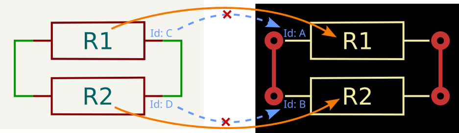
Re-linking the footprints by reference designator causes KiCad to re-create the links, using the matching reference designators as a guide.
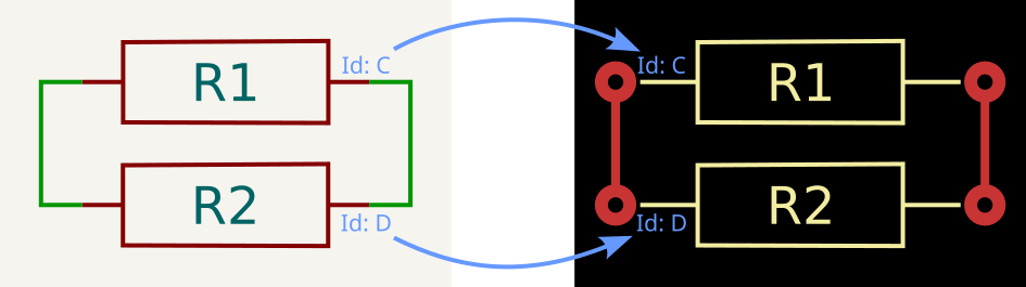
Because the links have been re-established, the next forward annotation should use the normal identifier-based linking (i.e. the checkbox should be unchecked).
从 PCB 上更新原理图(反向批注)
KiCad 的典型工作流程是在原理图中进行修改,然后使用 "从原理图更新 PCB" 工具将修改内容同步到电路板上。然而,相反的过程也是可行的:可以在电路板上进行设计修改,然后在原理图或电路板编辑器中使用 工具 → 从 PCB 更新原理图 同步回原理图。这个过程也被称为 "反向批注"。
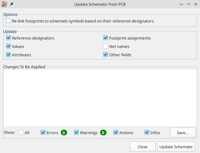
The tool syncs changes in reference designators, values, attributes (like DNP or Exclude From BOM), footprint assignments, other fields, and net names from the board to the schematic. Each type of change can be individually enabled or disabled.
将对原理图进行的修改列在 待应用的修改 窗格中。在您点击 更新原理图 按钮之前,原理图不会被修改。
你可以使用窗口底部的复选框来显示或隐藏不同类型的信息。可以使用 保存… 按钮将更改的报告保存到文件中。
选项
该工具有几个选项可以控制其行为。
Option |
描述 |
Re-link footprints to schematic symbols based on their reference designators |
If checked, each footprint in the PCB will be re-linked to the symbol that has the same reference designator as the footprint. This option is incompatible with updating symbol reference designators. If unchecked, footprints and symbols will be linked by unique identifier as usual, rather than by reference designator. This option should generally be left unchecked. See the PCB Editor documentation for more details on when to use this option. |
Reference designators |
If checked, symbol reference designators will be updated to match the reference designators of the linked footprints. If unchecked, symbol reference designators will not be updated. |
Values |
If checked, symbol values will be updated to match the values of the linked footprints. If unchecked, symbol values will not be updated. |
Attributes |
If checked, symbol attributes (like exclude from BOM and DNP) will be updated to match the corresponding attributes of the linked footprints. If unchecked, symbol attributes will not be updated. |
Other fields |
If checked, other symbol fields will be updated to match the corresponding fields of the linked footprints. Reference designator, value, and footprint are each controlled by their own separate option. If unchecked, other fields will not be updated in the schematic. |
Footprint assignments |
If checked, footprint assignments will be updated for symbols which have had their footprints changed or replaced in the board. If unchecked, symbol footprint assignments will not be updated. |
Net names |
If checked, the schematic will be updated with any net name changes that have been made in the board. Net labels will be updated or added to the schematic as necessary to match the board. If unchecked, net names will not be updated in the schematic. |
Prefer symbol unit swaps over label swaps |
The tool will detect situations where net connections within a multi-unit symbol have changed due to entire symbol units (gates) being swapped. Such swaps will be detected whether they were performed using the PCB Editor’s gate swap tool or whether the equivalent net changes were made manually. If checked, in these situations the schematic will be updated to match the PCB by swapping symbol units rather than swapping the net labels attached to the pins on each symbol unit. If unchecked, symbol unit swaps will be represented in the schematic by swapping net labels rather than swapping symbol units. |
Prefer symbol pin swaps over label swaps |
The tool will detect situations where net connections have swapped between two pins within a symbol. Such swaps will be detected whether they were performed using the pin swap tool or whether the equivalent net changes were made manually. If checked, in these situations the schematic will be updated to match the PCB by swapping symbol pins in the symbol rather than swapping the net labels attached to the pins, if possible. Symbol pins can only be swapped if the Allow unconstrained pin swaps option is enabled in the Editing Options page of the Schematic Editor’s preferences. If unchecked, symbol pin swaps will be represented in the schematic by swapping net labels rather than swapping pins in the symbol. |
| The 按位置重新批注 该功能可以与反向批注位号结合使用 根据设计中的元件的位置重新批注所有元件。 |
用 CMP 文件进行反向批注
通过从 PCB 编辑器中导出 CMP 文件(文件 → 导出 → 封装关联(.cmp)文件…)并在原理图编辑器中导入(文件 → 导入 → 封装分配…),也可以将变化从 PCB 同步到原理图。
| 这种方法只能同步对封装分配和封装字段的修改。建议使用 "从 PCB 更新原理图" 工具来代替。 |
生成输出
打印
KiCad 可以使用 文件 → 打印… 将原理图发送到标准打印机。
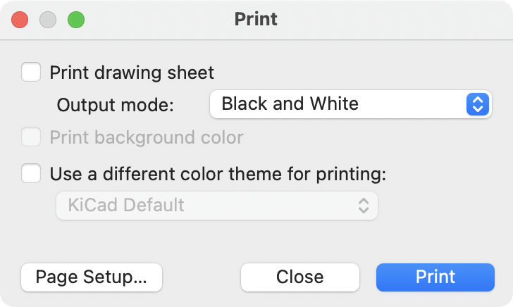
打印选项
-
Print drawing sheet: Include the drawing sheet border and title block in the printed schematic.
-
Output mode: Print the schematic in color or black and white.
-
Print background color: Include the background color in the printed schematic. This option is only enabled when printing in color.
-
Use a different color theme for printing: Select a different color scheme for printing than the one selected for display in the Schematic Editor.
-
Page Setup…: Opens a page setup dialog for setting paper size and orientation.
-
Close: Closes the dialog without printing.
-
Print: Opens the system print dialog.
| 打印时使用平台及打印机特有的驱动程序,可能会产生意想不到的结果。当打印到一个文件时,建议使用 绘图 而不是 打印。 |
绘图
KiCad 可以使用 文件 → 绘图… 将原理图绘制到文件中。
The supported output formats are Postscript, PDF, SVG, DXF, and PNG.
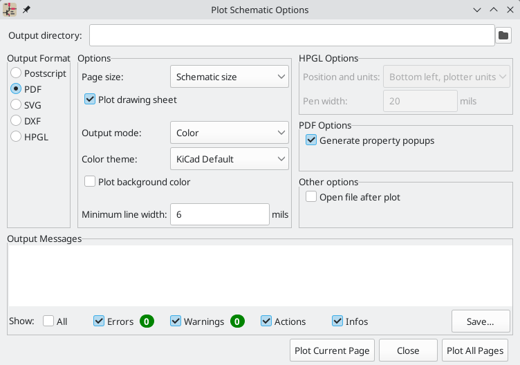
输出信息 窗格显示有关生成文件的信息。 可以用复选框显示或隐藏不同种类的信息,还可以用 保存… 按钮将信息保存到文件中。
点击绘制当前页 按钮绘制原理图的当前页。绘制全部页面 按钮可以绘制原理图的所有页面。每一页都会生成一个文件,但 PDF 输出除外,它将原理图的每一页作为单独的一页绘制在一个 PDF 文件中。
绘制选项
-
Output directory: Specify the location to save plotted files. If this is a relative path, it is created relative to the project directory. This path can use text variables, including both project text variables and built-in text variables.
-
Design variant: Select the design variant to plot.
-
Output Format: Select the format to plot in. Some formats have different options than others.
-
Page size: Sets the page size to use for the plotted output. This can be set to match the schematic size or to another sheet size.
-
Plot drawing sheet: Include the drawing sheet border and title block in the printed schematic.
-
Output mode: Sets the output to color or black and white. Not all output formats support color.
-
Color theme: Selects the color theme to use for the plotted output.
-
Plot background color: Includes the schematic background color in the plotted output. The background color will not be plotted if the output format does not support color or the output mode is black and white.
-
Minimum line width: Selects the minimum width for lines. Any lines narrower than this width will be plotted with this minimum width.
-
Generate property popups: Enables the interactive PDF features described below. This option only applies for PDF output.
-
Generate clickable links for hierarchical elements: Enables clickable hierarchical sheets, hierarchical sheet pins, and hierarchical labels. When enabled, clicking a hierarchical sheet or sheet pin in the PDF will open the PDF page for that subsheet. Clicking a hierarchical label will open the page for the parent sheet. If Generate property popups is also enabled, links will be generated instead of property popups for hierarchical sheets, pins, and labels (i.e. this option takes priority). This option only applies for PDF output.
-
Generate metadata from AUTHOR and SUBJECT variables: Sets the Author and Subject PDF document properties for the generated PDF based on the
AUTHORandSUBJECTproject text variables, if you have defined them. This option only applies for PDF output. -
Export units: Sets the units (inches or millimeters) in the exported DXF file.
-
DPI: Sets the pixel density of the output file (PNG only).
-
Anti-alias: Controls whether the output file should be anti-aliased (PNG only).
-
Open file after plot: automatically opens the plotted output file when plotting is complete.
PDF 交互功能
Plotted PDFs can optionally have several interactive features.
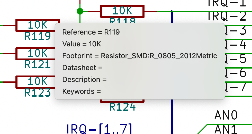
-
可以点击超链接。
-
目录中填充了原理图页以及每张页面中的符号和层次标签。
-
点击原理图对象会弹出一个包含相关信息的菜单。
-
符号显示其符号字段。
-
Hierarchical subsheets display their sheetname and filename, as well as an option to enter the sheet itself. This is replaced by a direct link to the subsheet if the Generate clickable links for hierarchical elements option is enabled.
-
标签显示已解决的网络和网络类。
-
总线显示其成员。
-
| Some of these features are not supported in all PDF readers. The clickable links generated by the Generate clickable links for hierarchical elements option are more widely supported than other interactive features. |
Generating a bill of materials
KiCad 可以生成物料清单,列出设计中的所有元件。物料清单是可配置的:您可以选择包括哪些元件、元件的排序方式、包括哪些符号字段和顺序,以及输出格式。
使用《符号字段表,符号字段表》导出物料清单。作为打开此对话框的 导出 选项卡的快捷方式,您可以选择* 工具 → 生成物料清单…* ,或使用顶部工具栏上的 ![]() 按钮。
按钮。
物料清单的内容在 编辑 选项卡中配置。导出 BOM 文件的格式在 导出 选项卡中配置。按下对话框底部的 导出 按钮后,BOM 即被写入。
BOM 内容
The exported BOM will contain the components (rows) and fields (columns) shown in the Edit tab, with the same grouping and sorting.
The Exclude from BOM and Do not Populate attributes affect the Edit tab and the exported BOM as follows:
-
Components with the Exclude from BOM attribute set are always excluded from BOM exports. They are shown in the Edit tab unless the Include 'Exclude from BOM' Symbols option is unchecked in the
menu. -
Components with the Do not Populate (DNP) attribute set are included in BOM exports and shown in the Edit tab unless the Include 'DNP' Symbols option is unchecked in the
menu.
You can filter the components that are exported by typing in the Filter textbox. This matches against symbols' references. Wildcards are supported: * matches any number of any characters, including none, and ? matches any single character.
You can also limit the displayed components to those in the current sheet, the current sheet and all of its subsheets, or the entire schematic using the dropdown menu next to the filter box.
The panel on the left side of the dialog contains a list of columns that are available to show in the Edit tab and include in the BOM. You can collapse this panel by clicking the ![]() button.
button.
Fields with the Include box checked will be shown in the Edit tab and included as columns in the BOM. You can also show or hide columns by right clicking the column header in the right part of the dialog and selecting the desired columns. To reorder the columns, drag a column header to the left or right. You can set an arbitrary name for each column by clicking in the BOM Name column and entering a new name.
Fields with the Group By box checked are used to group components together. Components are grouped into the same line if all of their Group By fields are identical and the Group symbols box at the top of the dialog is checked.
Presets
预置可用于配置字段列表。预置可存储显示的字段、用于分组的字段以及列顺序。 您可以创建并保存自己的预置,也可以使用多个默认预置之一。 自定义预置可以在此对话框或 《原理图设置,原理图设置》 对话框中删除。
There are several built-in presets:
-
"Grouped By Value" and "Grouped By Value and Footprint" replicate legacy BOM scripts. These group the symbols in the BOM by their
Valuefield and theirValueandFootprintfields, respectively. -
"Attributes" shows only the reference and value fields and the DNP, exclude from board, exclude from simulation, and exclude from BOM attributes.
Virtual fields
Some virtual fields are available that may be useful in BOM exports. Adding a field in the Symbol Fields Table beginning with a text variable will not create a new field in the symbols, but will create a special column in the table and BOM with auto-generated values for each component. The following variables may be especially useful for creating virtual fields in custom BOM formats:
-
${QUANTITY}创建一个字段,其中包含该元件的分组实例数。 -
${ITEM_NUMBER}创建一个包含 BOM 中元件行号的字段。 -
${SYMBOL_NAME}creates a field that contains the name of the schematic symbol. -
${SYMBOL_LIBRARY}creates a field that contains the name of the schematic symbol library. -
${DNP}创建一个带有复选框的字段,用于控制组件的 DNP 属性。在 BOM 中,如果元件的 DNP 属性已设置,则该字段解析为字符串 "DNP",否则解析为空字符串。 -
`${EXCLUDE_FROM_BOARD}`创建了一个带有复选框的字段,用于控制元件的从电路板排除属性。在 BOM 中,如果元件的电路板排除属性已设置,则该字段解析为字符串 "电路板排除",否则解析为空字符串。
-
`${EXCLUDE_FROM_SIM}`创建一个带有复选框的字段,用于控制元件的 "从仿真中排除 " 属性。在 BOM 中,如果与元件的 "从仿真中排除" 属性已设置,则该字段解析为字符串 "从仿真中排除",否则解析为空字符串。
-
${EXCLUDE_FROM_BOM}创建一个带有复选框的字段,用于控制元件的 BOM 排除属性。设置了排除在 BOM 之外属性的元件不会包含在 BOM 中。
Other text variables are also available.
The full functionality of the Edit tab, including virtual field behavior, is explained in more detail in the Symbol Fields Table documentation.
BOM format
导出 选项卡包含有关 BOM 输出文件格式的设置,并显示原始 BOM 输出文件的预览。
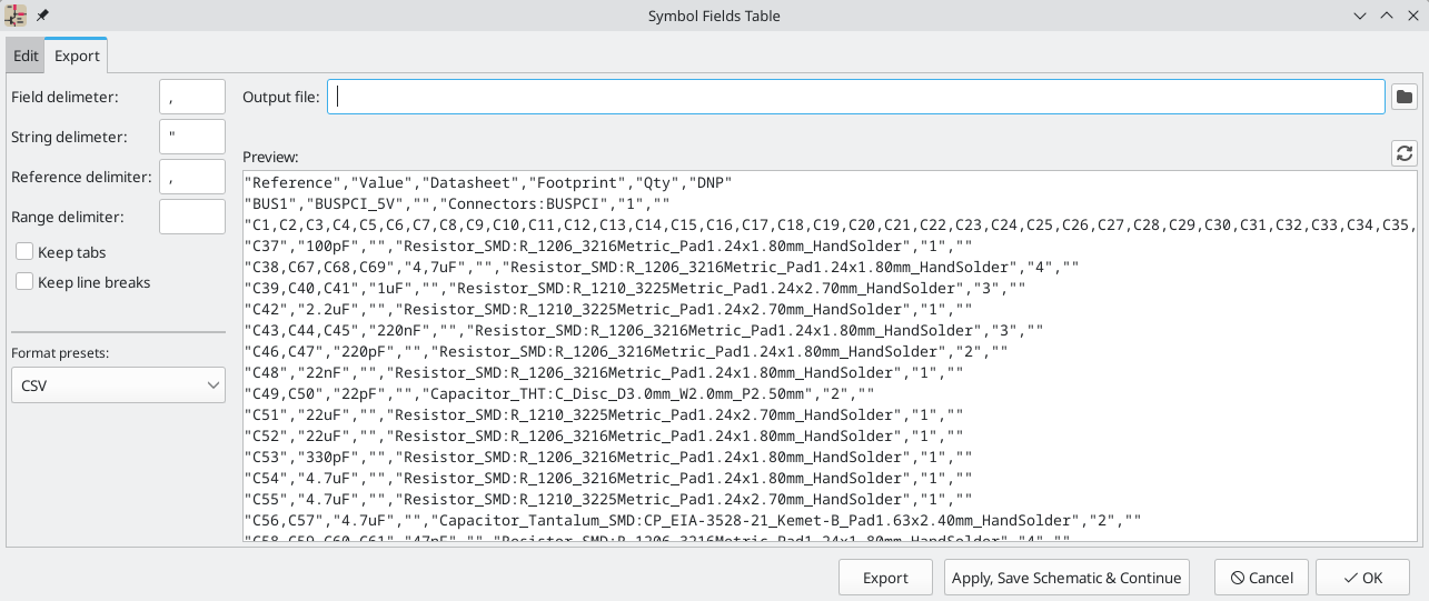
您可以在顶部指定输出文件。按下 导出 按钮将把 BOM 写入该文件路径。该路径可以包含 《文本变量,文本变量》。
左侧的设置控制 BOM 信息在文件中的格式。您可以更改字段之间的分隔符、围绕每个字段的分隔符、分隔引用序列的分隔符(例如,R1,R3 中的逗号)以及引用范围的分隔符(例如,R1-R3 中的破折号)。如果没有给出范围分隔符,则不会使用范围: 例如,R1-R3 将被写成`R1,R2,R3`,假定 , 为引用分隔符。根据 保留制表符 和 保留换行符 的设置,可以保留或删除字段中的制表符和换行符。
有多种默认格式预设可供选择。您可以选择逗号分隔值 (CSV) 格式、制表符分隔值 (TSV) 格式或分号分隔格式。您还可以创建和保存自己的预设。自定义预置可在此对话框或 《示意图设置,示意图设置》 对话框中删除。
Legacy BOM generation
以前版本的 KiCad 使用外部脚本将设计信息处理成所需的输出格式。选择 工具 → 生成传统物料清单… ,仍可使用此物料清单生成工具。
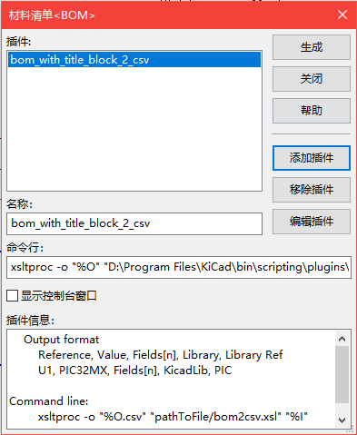
Several BOM generator scripts are included with KiCad, and users can also create their own. BOM generator scripts generally use Python or XSLT, but other tools can be used as long as you can specify a command line for KiCad to execute when running the generator.
您可以在 BOM 发生器脚本 列表中选择要使用的 BOM 生成器。 对话框的其余部分显示所选生成器的信息。您可以用 生成器昵称 文本框来改变生成器的显示名称。
右边的窗格显示所选脚本的信息。当生成器被执行时,右边的窗格会显示脚本的输出。
底部的文本框包含了 KiCad 用来执行生成器的命令。当选择脚本时,该文本框会自动填充,但对于某些生成器来说,该命令可能需要手工编辑。当关闭 BOM 工具时,KiCad 会保存每个生成器的命令行,因此定制的命令行会被保留下来。关于命令行的更多细节,请参阅 高级文档。
在 Windows 下,BOM 生成器对话框有一个额外的 *显示控制台窗口*选项。当这个选项未被选中时,BOM 生成器在一个隐藏的控制台窗口中运行,任何输出都会被重定向并打印在对话框中。当该选项被选中时,BOM 生成器在一个可见的控制台窗口中运行,如果生成器插件提供了一个图形用户界面,这可能是必要的。
BOM 生成器脚本
By default, the legacy BOM tool presents three output script options.
-
bom_csv_grouped_extraoutputs a CSV with a single section containing every component in the design. Components are grouped by value, footprint, DNP (do not populate), and any additional fields that are specified on the command line. To specify extra fields, add the desired field names as quoted strings at the end of the command line. For example, to include theMPNfield, the end of the command line would be:<path to script>/bom_csv_grouped_extra.py "%I" "%O.csv" "MPN". The columns in the BOM are:-
行编号
-
位号
-
数量
-
值
-
封装
-
不安装
-
指定的额外字段
-
-
bom_csv_grouped_by_value输出的CSV有两个部分。第一部分包含了设计中的每个元件,每行都有一个元件。 第二部分也包含每个元件,但元件是按符号名称、值、封装和 DNP(不安装)分组的。BOM 中的列是:-
行编号
-
数量
-
位号
-
值
-
符号库和符号名称
-
封装
-
数据手册
-
不安装
-
任何其他符号字段
-
-
bom_csv_grouped_by_value_with_fp输出一个 CSV,其中有一个单独的部分,包含设计中的每个元件。元件按值、封装和 DNP(不安装)进行分组。BOM 中的列是:-
位号
-
数量
-
值
-
符号名称
-
封装
-
符号描述
-
供应商
-
不安装
-
额外的生成器脚本与 KiCad 一起安装,但默认情况下不会在生成器脚本列表中填入。这些脚本的位置取决于操作系统,并可能根据安装位置而有所不同。
| Operating System | Location |
|---|---|
Windows |
|
Linux |
|
macOS |
|
通过点击 ![]() 按钮,可以在 BOM 生成器脚本列表中添加其他脚本。点击
按钮,可以在 BOM 生成器脚本列表中添加其他脚本。点击 ![]() 按钮,可以删除脚本。
按钮,可以删除脚本。![]() 按钮在文本编辑器中打开所选的脚本。
按钮在文本编辑器中打开所选的脚本。
关于创建和使用自定义 BOM 生成器的更多信息,请参见 高级文档。
从 PCB 编辑器导出 BOM
The PCB Editor can export a BOM through File → Fabrication Outputs → BOM…. This method provides no control over the output format and does not include all symbol information, but is useful for PCB-only workflows that do not involve a schematic. In general, it is recommended to use the schematic editor’s BOM export tool instead.
生成网表
网表是一个描述符号引脚之间电气连接的文件。 这些连接被称为网络。网表文件包含:
-
符号及其引脚的列表。
-
符号引脚之间的连接(网络)列表。
存在许多不同的网表格式。有时符号表和网表是两个独立的文件。网表是使用原理图设计软件的基础,因为网表建立了与其他电子 CAD 软件,如 PCB 布局软件、仿真器和可编程逻辑编译器的联系。
KiCad 支持几种网表格式:
-
KiCad 格式,可由 KiCad PCB 编辑器导入。然而,应该使用 "从原理图更新 PCB" 工具而不是将 KiCad 网表导入 PCB 编辑器。
-
OrCAD PCB2 格式,用于 OrCAD 设计 PCB。
-
Allegro format, for designing PCBs with Allegro.
-
PADS format, for designing PCBs with PADS.
-
CADSTAR 格式,用于 CADSTAR 设计 PCB。
-
Spice 格式,用于各种外部电路仿真器。
| 在 KiCad 5.0 及以后的版本中,将设计从原理图编辑器转移到 PCB 编辑器时,没有必要创建网表。推荐使用 "从原理图更新PCB" 工具。 |
| 其他使用网表的软件工具可能对元件名称、引脚、网络和其他字段中的空格和特殊字符有限制。为了兼容性,请注意其他工具中的这种限制,并相应地命名元件、网络等。 |
网表格式
网表是通过导出网表对话框(文件 → 导出 → 网表…)导出的。
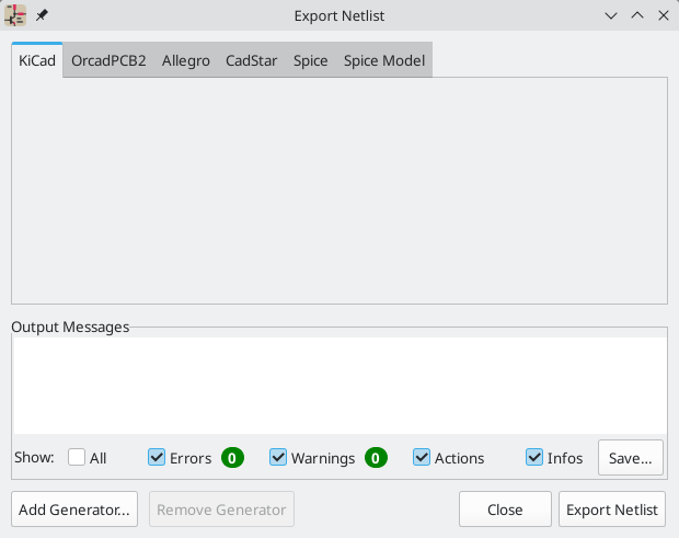
KiCad supports exporting netlists in several formats: KiCad, OrcadPCB2, Allegro, PADS, CADSTAR, Spice, and Spice Model. Each format can be selected by selecting the corresponding tab at the top of the window. Some netlist formats have additional options.
点击 导出网表 按钮,会提示输入网表文件名并保存网表。
| 对于大型原理图,网表的生成可能需要几分钟。 |
其他网表格式的自定义生成器可以通过点击 添加生成器… 按钮添加。自定义生成器是由 KiCad 调用的外部工具,例如 Python 脚本或 XSLT 样式表。关于自定义网表生成器的更多信息,请参见添加自定义网表生成器章节。
Spice 网表格式
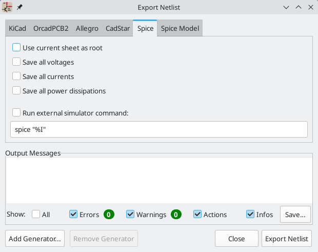
Spice 网表格式提供了几个选项。
-
当选择 使用当前图纸作为根图纸 时,只有当前页图纸导出到子电路模型中。否则,所有原理图图纸将被导出。
-
The Save all voltages option adds a
.save allcommand to the netlist, which causes the simulator to save all node voltages. -
The Save all currents option adds a
.probe allicommand to the netlist, which causes the simulator save all node currents. -
The Save all power dissipations adds
.probecommands to save the power dissipation in each component. -
The Save all digital event data removes the
esave nonecommand from the netlist, which causes digital event data to be saved. Digital event data may consume a lot of memory.
| 不同仿真工具之间的行为可能有所不同。 |
无源符号值会自动调整,以便与各种 Spice 仿真器兼容。具体而言:
-
μandMas unit prefixes are replaced withuandMeg, respectively -
Units are removed (e.g.
4.7kΩis changed to4.7k) -
RKM 格式的数值被改写为与 Spice 兼容(例如,
4u7被改成4.7u)
Spice 网表导出器还提供了一种简单的方法,可以用外部仿真器对生成的网表进行仿真。这对于在不使用KiCad 的内部 ngspice 仿真器的情况下运行仿真,或者使用 KiCad 的仿真器工具不支持的选项运行 ngspice 仿真是很有用的。
Enter the path to the external simulator in the text box, with %I representing the generated netlist. Check the run external simulator command box to generate the netlist and automatically run the simulator.
默认的仿真器命令(spice "%I")必须调整为指向系统上安装的仿真器。
|
Spice 仿真器预期仿真命令(.PROBE, .AC, .TRAN 等)包含在网表中。原理图中包含的任何以句号(.)开始的文本行都将被包含在网表中。如果一个文本对象包含多行,只有以句号开头的行将被包含在内。
根据原理图中符号的 Spice 模型设置,用于包括模型库文件的 .include 指令被自动添加到网表。
Spice 模型网表格式
KiCad 还可以将原理图的网表导出为 Spice 子电路模型,这可以包含在一个单独的 Spice 仿真中。原理图中的任何层次标签都被用作子电路模型的引脚。模型中的每个引脚都有批注,描述该引脚的电气方向:
-
输入的层次标签被映射到一个输入的批注上 -
输出的层次化标签被映射到输出批注上 -
双向层次标签被映射到输入输出批注上 -
三态的层次标签被映射到三态批注上 -
被动层次标签被映射到被动批注上
当选择 使用当前图纸作为根图纸 时,只有当前页图纸导出到子电路模型中。否则,所有原理图图纸将被导出。
网表示例
下面是 KiCad 仿真示例的 sallen_key 工程的原理图。
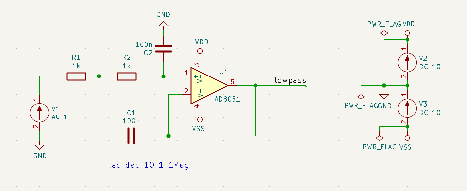
该原理图的 KiCad 格式网表如下:
(export (version "E")
  (design
    (source "/usr/share/kicad/demos/simulation/sallen_key/sallen_key.kicad_sch")
    (date "Sun 01 May 2022 03:14:05 PM EDT")
    (tool "Eeschema (6.0.4)")
    (sheet (number "1") (name "/") (tstamps "/")
      (title_block
        (title)
        (company)
        (rev)
        (date)
        (source "sallen_key.kicad_sch")
        (comment (number "1") (value ""))
        (comment (number "2") (value ""))
        (comment (number "3") (value ""))
        (comment (number "4") (value ""))
        (comment (number "5") (value ""))
        (comment (number "6") (value ""))
        (comment (number "7") (value ""))
        (comment (number "8") (value ""))
        (comment (number "9") (value "")))))
  (components
    (comp (ref "C1")
      (value "100n")
      (libsource (lib "sallen_key_schlib") (part "C") (description ""))
      (property (name "Sheetname") (value ""))
      (property (name "Sheetfile") (value "sallen_key.kicad_sch"))
      (sheetpath (names "/") (tstamps "/"))
      (tstamps "00000000-0000-0000-0000-00005789077d"))
    (comp (ref "C2")
      (value "100n")
      (fields
        (field (name "Fieldname") "Value")
        (field (name "SpiceMapping") "1 2")
        (field (name "Spice_Primitive") "C"))
      (libsource (lib "sallen_key_schlib") (part "C") (description ""))
      (property (name "Fieldname") (value "Value"))
      (property (name "Spice_Primitive") (value "C"))
      (property (name "SpiceMapping") (value "1 2"))
      (property (name "Sheetname") (value ""))
      (property (name "Sheetfile") (value "sallen_key.kicad_sch"))
      (sheetpath (names "/") (tstamps "/"))
      (tstamps "00000000-0000-0000-0000-00005789085b"))
    (comp (ref "R1")
      (value "1k")
      (fields
        (field (name "Fieldname") "Value")
        (field (name "SpiceMapping") "1 2")
        (field (name "Spice_Primitive") "R"))
      (libsource (lib "sallen_key_schlib") (part "R") (description ""))
      (property (name "Fieldname") (value "Value"))
      (property (name "SpiceMapping") (value "1 2"))
      (property (name "Spice_Primitive") (value "R"))
      (property (name "Sheetname") (value ""))
      (property (name "Sheetfile") (value "sallen_key.kicad_sch"))
      (sheetpath (names "/") (tstamps "/"))
      (tstamps "00000000-0000-0000-0000-0000578906ff"))
    (comp (ref "R2")
      (value "1k")
      (fields
        (field (name "Fieldname") "Value")
        (field (name "SpiceMapping") "1 2")
        (field (name "Spice_Primitive") "R"))
      (libsource (lib "sallen_key_schlib") (part "R") (description ""))
      (property (name "Fieldname") (value "Value"))
      (property (name "SpiceMapping") (value "1 2"))
      (property (name "Spice_Primitive") (value "R"))
      (property (name "Sheetname") (value ""))
      (property (name "Sheetfile") (value "sallen_key.kicad_sch"))
      (sheetpath (names "/") (tstamps "/"))
      (tstamps "00000000-0000-0000-0000-000057890691"))
    (comp (ref "U1")
      (value "AD8051")
      (fields
        (field (name "Spice_Lib_File") "ad8051.lib")
        (field (name "Spice_Model") "AD8051")
        (field (name "Spice_Netlist_Enabled") "Y")
        (field (name "Spice_Primitive") "X"))
      (libsource (lib "sallen_key_schlib") (part "Generic_Opamp") (description ""))
      (property (name "Spice_Primitive") (value "X"))
      (property (name "Spice_Model") (value "AD8051"))
      (property (name "Spice_Lib_File") (value "ad8051.lib"))
      (property (name "Spice_Netlist_Enabled") (value "Y"))
      (property (name "Sheetname") (value ""))
      (property (name "Sheetfile") (value "sallen_key.kicad_sch"))
      (sheetpath (names "/") (tstamps "/"))
      (tstamps "00000000-0000-0000-0000-00005788ff9f"))
    (comp (ref "V1")
      (value "AC 1")
      (libsource (lib "sallen_key_schlib") (part "VSOURCE") (description ""))
      (property (name "Sheetname") (value ""))
      (property (name "Sheetfile") (value "sallen_key.kicad_sch"))
      (sheetpath (names "/") (tstamps "/"))
      (tstamps "00000000-0000-0000-0000-000057336052"))
    (comp (ref "V2")
      (value "DC 10")
      (fields
        (field (name "Fieldname") "Value")
        (field (name "Spice_Node_Sequence") "1 2")
        (field (name "Spice_Primitive") "V"))
      (libsource (lib "sallen_key_schlib") (part "VSOURCE") (description ""))
      (property (name "Fieldname") (value "Value"))
      (property (name "Spice_Primitive") (value "V"))
      (property (name "Spice_Node_Sequence") (value "1 2"))
      (property (name "Sheetname") (value ""))
      (property (name "Sheetfile") (value "sallen_key.kicad_sch"))
      (sheetpath (names "/") (tstamps "/"))
      (tstamps "00000000-0000-0000-0000-0000578900ba"))
    (comp (ref "V3")
      (value "DC 10")
      (fields
        (field (name "Fieldname") "Value")
        (field (name "Spice_Node_Sequence") "1 2")
        (field (name "Spice_Primitive") "V"))
      (libsource (lib "sallen_key_schlib") (part "VSOURCE") (description ""))
      (property (name "Fieldname") (value "Value"))
      (property (name "Spice_Primitive") (value "V"))
      (property (name "Spice_Node_Sequence") (value "1 2"))
      (property (name "Sheetname") (value ""))
      (property (name "Sheetfile") (value "sallen_key.kicad_sch"))
      (sheetpath (names "/") (tstamps "/"))
      (tstamps "00000000-0000-0000-0000-000057890232")))
  (libparts
    (libpart (lib "sallen_key_schlib") (part "C")
      (footprints
        (fp "C?")
        (fp "C_????_*")
        (fp "C_????")
        (fp "SMD*_c")
        (fp "Capacitor*"))
      (fields
        (field (name "Reference") "C")
        (field (name "Value") "C"))
      (pins
        (pin (num "1") (name "") (type "passive"))
        (pin (num "2") (name "") (type "passive"))))
    (libpart (lib "sallen_key_schlib") (part "Generic_Opamp")
      (fields
        (field (name "Reference") "U")
        (field (name "Value") "Generic_Opamp"))
      (pins
        (pin (num "1") (name "+") (type "input"))
        (pin (num "2") (name "-") (type "input"))
        (pin (num "3") (name "V+") (type "power_in"))
        (pin (num "4") (name "V-") (type "power_in"))
        (pin (num "5") (name "") (type "output"))))
    (libpart (lib "sallen_key_schlib") (part "R")
      (footprints
        (fp "R_*")
        (fp "Resistor_*"))
      (fields
        (field (name "Reference") "R")
        (field (name "Value") "R"))
      (pins
        (pin (num "1") (name "") (type "passive"))
        (pin (num "2") (name "") (type "passive"))))
    (libpart (lib "sallen_key_schlib") (part "VSOURCE")
      (fields
        (field (name "Reference") "V")
        (field (name "Value") "VSOURCE")
        (field (name "Fieldname") "Value")
        (field (name "Spice_Primitive") "V")
        (field (name "Spice_Node_Sequence") "1 2"))
      (pins
        (pin (num "1") (name "") (type "input"))
        (pin (num "2") (name "") (type "input")))))
  (libraries
    (library (logical "sallen_key_schlib")
      (uri "/usr/share/kicad/demos/simulation/sallen_key/sallen_key_schlib.kicad_sym")))
  (nets
    (net (code "1") (name "/lowpass")
      (node (ref "C1") (pin "1") (pintype "passive"))
      (node (ref "U1") (pin "2") (pinfunction "-") (pintype "input"))
      (node (ref "U1") (pin "5") (pintype "output")))
    (net (code "2") (name "GND")
      (node (ref "C2") (pin "2") (pintype "passive"))
      (node (ref "V1") (pin "2") (pintype "input"))
      (node (ref "V2") (pin "2") (pintype "input"))
      (node (ref "V3") (pin "1") (pintype "input")))
    (net (code "3") (name "Net-(C1-Pad2)")
      (node (ref "C1") (pin "2") (pintype "passive"))
      (node (ref "R1") (pin "1") (pintype "passive"))
      (node (ref "R2") (pin "2") (pintype "passive")))
    (net (code "4") (name "Net-(C2-Pad1)")
      (node (ref "C2") (pin "1") (pintype "passive"))
      (node (ref "R2") (pin "1") (pintype "passive"))
      (node (ref "U1") (pin "1") (pinfunction "+") (pintype "input")))
    (net (code "5") (name "Net-(R1-Pad2)")
      (node (ref "R1") (pin "2") (pintype "passive"))
      (node (ref "V1") (pin "1") (pintype "input")))
    (net (code "6") (name "VDD")
      (node (ref "U1") (pin "3") (pinfunction "V+") (pintype "power_in"))
      (node (ref "V2") (pin "1") (pintype "input")))
    (net (code "7") (name "VSS")
      (node (ref "U1") (pin "4") (pinfunction "V-") (pintype "power_in"))
      (node (ref "V3") (pin "2") (pintype "input")))))
在 Spice 格式中,网表如下:
.title KiCad schematic
.include "ad8051.lib"
XU1 Net-_C2-Pad1_ /lowpass VDD VSS /lowpass AD8051
C2 Net-_C2-Pad1_ GND 100n
C1 /lowpass Net-_C1-Pad2_ 100n
R2 Net-_C2-Pad1_ Net-_C1-Pad2_ 1k
R1 Net-_C1-Pad2_ Net-_R1-Pad2_ 1k
V1 Net-_R1-Pad2_ GND AC 1
V2 VDD GND DC 10
V3 GND VSS DC 10
.ac dec 10 1 1Meg
.end
Design variants
Many products share a common circuit board but are sold in different configurations. A consumer router might come in WiFi-only and WiFi+Bluetooth models; an industrial controller might ship with different sensor front-ends for different markets. Traditionally, each configuration requires its own schematic and board, which means duplicated work and diverging designs.
Design variants solve this problem. A variant is a named set of overrides applied on top of a single base design. Each variant can change which components are populated, swap field values such as the component value or footprint, and control which components appear in the BOM or position files. The base design remains the source of truth, and each variant records only what differs.
| Design variants are an assembly-level feature. All variants share the same copper, the same netlist, and the same board outline. If your product configurations require different copper or different board shapes, you need separate board designs. |
Understanding design variants
Every KiCad project starts with a single implicit variant called the default variant. The default variant represents the base design with no overrides. When you create additional named variants, each one begins as an exact copy of the default and can then be customized independently.
Variant data is stored per symbol instance in the schematic. This means that the same symbol used in different places in a hierarchical design can have different variant overrides at each location. When you run Update PCB from Schematic, the variant data is transferred to the corresponding footprints on the board.
The active variant is selected from a dropdown in the main toolbar of both the Schematic Editor and the PCB Editor. Selecting a variant immediately updates the display to reflect that variant’s overrides, including field text, DNP markings, and exclusion indicators.
Types of variation
Fitted and not fitted
The most common use of variants is to mark certain components as Do Not Populate (DNP) in one variant while keeping them fitted in another. A component marked DNP in the active variant is displayed with an X through it on the schematic and on the fabrication layers of the board.
For example, a Bluetooth module and its supporting passives might be fitted in a "WiFi+BT" variant but marked DNP in a "WiFi-only" variant.
Field overrides
Variants can override any symbol field on a per-component, per-variant basis. Common uses include changing the Value field to select a different resistance or capacitance, changing the Footprint field to substitute a different package, or updating a custom Manufacturer Part Number field to point to an alternate sourcing option.
When a field has been overridden for the active variant, the Symbol Fields Table highlights the cell with a colored background so you can see at a glance which values differ from the base design.
| The Reference field cannot be overridden by a variant. Changing a reference designator would effectively create a different netlist, which is outside the scope of assembly variants. |
Excluding from outputs
In addition to the DNP flag, each variant can independently control whether a component is excluded from:
-
BOM — the component will not appear in the bill of materials for that variant
-
Position files — the component will be omitted from pick-and-place output
-
Simulation — the component will be excluded from SPICE simulation
These flags are independent of each other and independent of DNP. For instance, you might want a test point to appear in the BOM but not in the position file for a specific variant.
Sheet-level variants
Variant overrides can also be applied to entire hierarchical sheets. Marking a sheet as DNP for a variant marks every component on that sheet (and all nested sub-sheets) as not fitted. This is useful when a hierarchical sheet represents a functional block that is present in some product configurations and absent in others.
Sheet-level exclusion flags (BOM, position files, simulation) work the same way, applying to all components within the sheet for that variant.
Creating and managing variants
Creating a new variant
There are two ways to create a new variant:
-
From the toolbar: Click the variant selector dropdown in the main toolbar and choose Add New Design Variant… at the bottom of the list. A dialog appears where you enter a name and an optional description.
-
From the Symbol Fields Table: Open the Symbol Fields Table (Tools → Bulk Edit Symbol Fields…), then click the Add button in the variant list on the left side of the dialog.
Variant names must be unique (comparison is case-insensitive) and cannot use the reserved name <Default>.
Switching between variants
Select the desired variant from the dropdown in the main toolbar. The schematic view updates immediately to show the overridden field values and DNP markings for that variant. Selecting <Default> returns to the base design with no overrides.
Managing variants in the Symbol Fields Table
The Symbol Fields Table provides a variant list on the left side of the dialog with buttons for common management operations:
-
Add — create a new variant (same dialog as the toolbar method).
-
Delete — remove the selected variant and all of its overrides.
-
Rename — change the name of the selected variant.
-
Copy — duplicate the selected variant under a new name, preserving all of its overrides.
-
Edit Variant Description — change the description of the selected variant. You can also edit the description of the active variant using Tools → Variants → Edit Variant Description…
| The default variant cannot be deleted, renamed, or copied. It always exists as the base design. |
Selecting a variant in the list switches the grid to display that variant’s data. Any pending edits to the previously active variant are committed automatically.
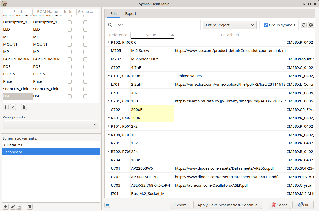
Editing variant data
When a non-default variant is selected in the toolbar, editing the schematic modifies that variant rather than the base design. Edit variant data in bulk through the Symbol Fields Table, or one symbol at a time with the normal schematic editing tools.
Editing fields in the Symbol Fields Table
The Symbol Fields Table is the primary tool for bulk-editing variant data. Select a variant from the list on the left, then edit cell values directly in the grid. The grid shows the effective value for each field in the selected variant.
Cells that differ from the default variant are highlighted with a colored background (yellow in light themes, gold in dark themes). This makes it easy to review all overrides at a glance.
To set a field back to its default value, clear the cell or set it to match the default variant’s value. The override is removed and the highlight disappears.
The same grid supports editing DNP and exclusion flags. The DNP, Exclude from BOM, Exclude from Position Files, and Exclude from Simulation columns contain checkboxes that can be toggled per variant.
Editing variants in the canvas
While a non-default variant is active, any edit made in the canvas updates that variant’s overrides. The base design is unchanged. This applies to all the normal editing tools:
-
The Properties panel on the left shows the effective field values and attribute flags for the active variant. Edits here update the variant’s overrides for the selected symbol.
-
The Symbol Properties dialog (double-click a symbol) shows the active variant name in its title bar so you know edits apply to that variant.
-
In-place field edits on the canvas and attribute changes from the right-click menu also apply to the active variant.
To mark a component as DNP for a specific variant, select the variant from the toolbar dropdown, select the symbol, and check the Do not populate checkbox in the Properties panel. The symbol is immediately drawn with an X overlay; switching back to the default variant shows the symbol without the X (assuming it is fitted in the base design). The same procedure works for the Exclude from BOM, Exclude from position files, and Exclude from simulation checkboxes.
For bulk editing across many components at once, use the Symbol Fields Table.
Generating variant-aware outputs
BOM export with variants
Open the Symbol Fields Table via Tools → Generate Bill of Materials…. The exported BOM reflects the active variant’s field values and respects its DNP and BOM exclusion flags.
To generate separate BOM files for each variant automatically, use the ${VARIANT} text variable in the output file path. For example, an output path of bom_${VARIANT}.csv produces bom_WiFi-only.csv and bom_WiFi-BT.csv when the project has those two variants defined.
Schematic plotting with variants
The Plot Schematic dialog (File → Plot…) includes a variant selector. Choose a variant to generate schematic plots that show the correct field values and DNP markings for that configuration. The default variant produces a plot of the base design.
Command-line variant support
Several sch export commands in the KiCad command-line interface support the --variant argument, including sch export bom, sch export pdf, sch export svg, sch export dxf, sch export ps, and sch export netlist. This enables scripted generation of schematic output for one or more variants.
To export a schematic PDF for a specific variant:
kicad-cli sch export pdf --variant "WiFi-only" my_project.kicad_schTo generate output for multiple variants in a single command, specify --variant more than once and use ${VARIANT} in the output path to produce separate files:
kicad-cli sch export pdf \
    --variant "WiFi-only" \
    --variant "WiFi-BT" \
    -o "schematic_${VARIANT}.pdf" \
    my_project.kicad_sch
When --variant is not specified, the default variant is used.
For a complete list of sch export commands and their variant-related options, see the Command-Line Interface reference.
文本变量
Two text variables are available for use in title blocks, text labels, and other text items:
-
${VARIANT}— resolves to the name of the currently active variant, or an empty string when the default variant is active -
${VARIANT_DESC}— resolves to the description of the currently active variant
These variables update dynamically when you switch variants and are included in plotted output, making it straightforward to identify which variant a printed schematic represents.
Transferring variants to the PCB editor
Variant data is transferred from the schematic to the PCB when you run Update PCB from Schematic (Tools → Update PCB from Schematic…). The update process synchronizes DNP flags, exclusion flags, and field overrides from each symbol to the corresponding footprint. This happens for every variant.
If a variant override has been removed in the schematic, the corresponding footprint override is reset to the base value during the update.
| Variant data flows from the schematic to the PCB, not the other way around. Always define and edit variants in the Schematic Editor, then update the PCB. |
After the update, the PCB Editor’s toolbar variant selector is populated with the same variant names. See Design variants in the PCB Editor manual for details on working with variants in the board layout.
符号和符号库
KiCad 将符号组织到符号库中,符号库是符号的集合。原理图中的每个符号都由一个完整的名称作为唯一标识,完整的名称由库的名称和符号名称组成。例如,标识符 Audio:AD1853 是指 Audio 库中的 AD1853 符号。
管理符号库
KiCad uses a table of symbol libraries to map a symbol library nickname to an underlying symbol library on disk. Kicad uses a global symbol library table as well as a table specific to each project. Libraries are not loaded unless they are included in either the global or project-specific library table.
To edit either symbol library table, use Preferences → Manage Symbol Libraries….
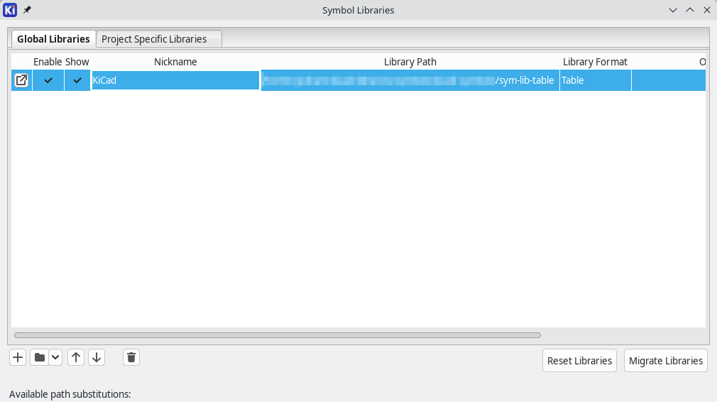
全局符号库表包含了无论当前加载的工程是什么,都可以使用的库列表。该表保存在 KiCad 配置文件夹下的 sym-lib-table 文件中。该文件夹的位置 取决于使用的操作系统。
工程专用的符号库表包含了专门为当前加载工程提供的库的列表。如果有任何工程专用的符号库,该表将保存在工程文件夹下的 sym-lib-table 文件中。
Many (or even all) of the loaded libraries may be contained in a nested library table, as shown in the screenshot above. To expand a nested library table and view its contents, press the ![]() button next to the nested library table entry. This opens the nested table in a new tab, as shown below.
button next to the nested library table entry. This opens the nested table in a new tab, as shown below.
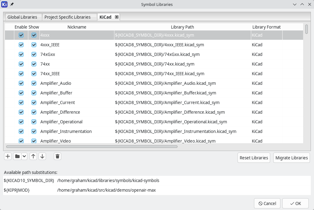
KiCad’s symbol library management system allows directly using many types of symbol libraries, including formats that are native to other non-KiCad EDA tools:
-
KiCad symbol libraries (
.kicad_symfiles, or folders of.kicad_symfiles) -
KiCad Legacy symbol libraries (
.libfiles) -
Altium Designer libraries (
.SchLibor.IntLibfiles) -
CADSTAR Schematic Archive libraries (
.libfiles) -
KiCad database library configuration files (
.kicad_dblfiles) -
Eagle libraries (
.xmlfiles) -
EasyEDA (JLCEDA) Standard Edition libraries (
.jsonfiles) -
EasyEDA (JLCEDA) Professional Edition libraries (
.elibz,.epro, or.zipfiles) -
KiCad HTTP library configuration files (
.kicad_httplibfiles)
Non-KiCad symbol libraries, including KiCad Legacy symbol libraries, can be migrated to KiCad .kicad_sym format using the Migrate Libraries button (see the migrating libraries section).
KiCad only supports writing to KiCad’s native .kicad_sym format symbol libraries. All other symbol library formats are read-only. To modify a non-KiCad format symbol library, you must first convert it to KiCad format.
|
Library tables can also include other library tables, which are called nested library tables. When a nested library table is used, the libraries in the nested table are loaded as if they were included directly in the main table.
Initial configuration
The first time KiCad runs (or any time KiCad runs and no configuration is found), KiCad will guide you through creating a new configuration or importing a configuration from a previous version. This includes setting up a new footprint library table. This process is described in the Project Manager documentation.
You can reset your footprint library table to the default by clicking the Reset Libraries button in the footprint library table dialog.
| Resetting your footprint library table will permanently change your footprint library table on disk. |
The default symbol library table contains a single entry, which points to another symbol library table containing all of KiCad’s default symbol libraries. This nested library table is maintained as part of the KiCad libraries and is updated along with KiCad and its libraries. You should not edit it yourself.
| KiCad’s default symbol libraries are included in your library table via a nested library. This allows the list of default KiCad libraries to be updated when KiCad and its libraries are updated, without affecting your personal library configuration. Your personal library table configuration can be maintained between KiCad versions, while still allowing you to receive updates to the default libraries. |
Managing table entries
Symbol libraries can only be used if they have been added to either the global or project-specific symbol library table (or to a nested table included in either top-level table).
通过点击 ![]() 按钮然后选择一个库或点击
按钮然后选择一个库或点击 ![]() 按钮然后输入库文件的路径来添加一个库。选定的库将被添加到当前打开的库表中(全局或特定工程)。可以通过选择所需的库条目并点击
按钮然后输入库文件的路径来添加一个库。选定的库将被添加到当前打开的库表中(全局或特定工程)。可以通过选择所需的库条目并点击 ![]() 按钮来删除库。
按钮来删除库。
When an entry in the library table is itself another library table, you can open this nested table by clicking the ![]() button next to the nested table’s entry. This opens the nested table in a new tab, where you can see and edit the libraries included in the nested table. To add a nested library table, click the downwards arrow next to the
button next to the nested table’s entry. This opens the nested table in a new tab, where you can see and edit the libraries included in the nested table. To add a nested library table, click the downwards arrow next to the ![]() button, choose the Table library type, then browse to the table file.
button, choose the Table library type, then browse to the table file.
The ![]() and
and ![]() buttons move the selected library up and down in the library table. This does not affect the display order of libraries in the Symbol Editor or Symbol Chooser.
buttons move the selected library up and down in the library table. This does not affect the display order of libraries in the Symbol Editor or Symbol Chooser.
Libraries can be disabled by unchecking the Enable checkbox in the first column. Inactive libraries are still in the library table but do not appear in any library browsers and are not loaded from disk, which can reduce loading times. Alternatively, you can hide a library from the library browsers while still loading it from disk by unchecking the Show checkbox.
| Hiding a library is primarily useful in conjunction with database libraries. Database libraries define symbols by adding metadata to symbol definitions from another symbol library. This base symbol library needs to be loaded, so it cannot be disabled, but for convenience the library can be hidden if it is not needed beyond the database library definition. |
通过点击范围内的第一个库,然后 Shift - 点击范围内的最后一个库,可以选择一系列的库。
每个库必须有一个独特的名称:在同一个表中不允许有重复的库名称。然而,名称可以在全局和工程库表中重复。工程表中的库比全局表中的同名库优先级更高。
库的名称不一定要与库的文件名或路径有关。冒号字符(:)不能在库的名称或符号名称中使用,因为它被用作名称和符号之间的分隔符。
Each library entry must have a valid path. Paths can be defined as absolute, relative, or by path variable substitution.
The appropriate library format must be selected in order for the library to be properly read. The supported formats are listed above. Only KiCad format libraries (.kicad_sym) can be saved. Other symbol library formats are read-only and must be converted to KiCad format before you can modify them.
有一个可选的描述字段,用于添加库条目的描述。选项字段目前不使用,所以添加选项在加载库时不会有任何影响。
Nested library tables
In addition to containing libraries, library tables can also contain other library tables. Library tables that are referenced by other library tables in this way are called nested library tables. Any libraries in a nested library table are loaded as if they were directly listed in the top-level library table.
Nested library tables let you separate groups of libraries into different library table files, then include all of the individual tables into the main top-level library table. This could be used, for example, to make a standard library table for your company, and share that table with everyone who needs it. Each user can then access the standard set of company libraries after they add the shared table as a nested library table in their own global table.
When KiCad is configured to its default library table configuration, the global library table contains a single entry, which is a nested library table. This nested table is part of KiCad’s default libraries and lists all of the KiCad default symbol libraries. When KiCad is updated, this nested table is also updated, which allows you to receive an updated list of KiCad’s default libraries without disturbing your personal library configuration.
Path variable substitution
The symbol library tables support path variable substitution, which allows you to define path variables containing custom paths to where your libraries are stored. Path variable substitution is supported by using the syntax ${PATH_VAR_NAME} in the symbol library path.
By default, KiCad defines several path variables which are described in the project manager documentation. Path variables can be configured in the Preferences → Configure Paths… dialog.
Using path variables in the symbol library tables allows libraries to be relocated without breaking the symbol library tables, so long as the path variables are updated when the library location changes.
KiCad will automatically resolve versioned path variables from
older versions of KiCad to the value of the corresponding variable from
the current KiCad version, as long as the old variable is not explicitly
defined itself. For example, ${KICAD9_SYMBOL_DIR} will
automatically resolve to the value of ${KICAD10_SYMBOL_DIR} if there
is no KICAD9_SYMBOL_DIR variable defined.
|
${KIPRJMOD} is a special path variable that always expands to the absolute path of the current project directory. ${KIPRJMOD} allows libraries to be stored in the project folder without having to use an absolute path in the project library table. This makes it possible to relocate projects without breaking their project library tables.
Usage patterns
符号库可以全局定义,也可以专门为当前加载的工程定义。在用户的全局表中定义的符号库总是可用的,并存储在用户的 KiCad 配置文件夹中的 sym-lib-table 文件中。工程专用的符号库表只对当前打开的工程文件有效。
每种方法都有其优点和缺点。在全局表中定义所有的库意味着它们在需要时总是可用的。这样做的缺点是,加载时间会增加。
在工程的基础上定义所有的符号库,意味着你只有工程所需的库,这减少了符号库的加载时间。缺点是你总是要记住添加每个工程所需的每个符号库。
一种使用模式是在全局范围内定义常用的库,并在工程专用的库表中定义工程所需的库。对于如何定义库没有任何限制。
Migrating symbol libraries to KiCad format
Non-KiCad format libraries, including legacy libraries (.lib files), are read-only. They need to be converted to KiCad format (.kicad_sym files) before you can save changes to them.
| As with most KiCad files, newer versions of KiCad can open older-format library files, but older versions of KiCad cannot read files once they have been saved by a newer version of KiCad. |
Libraries in other formats can be converted to KiCad libraries by selecting them in the symbol library table and clicking the Migrate Libraries button. Multiple libraries can be selected and migrated at once by Ctrl-clicking or shift-clicking.
也可以一次转换一个库,方法是在符号编辑器中打开它们并将它们另存为新库。
Unpacked libraries
A KiCad symbol library is typically in the form of a single .kicad_sym file that contains multiple symbols. This is known as a packed library, in the sense that multiple symbols are packed into a single file.
Beginning in KiCad 10.0, symbol libraries can also take the form of a folder containing multiple .kicad_sym files, with each file containing one or more symbols. The folder and the .kicad_sym files in it comprise a single symbol library, but each .kicad_sym file is otherwise in the same format as a packed library. This is known as an unpacked library.
By convention, unpacked symbol libraries use the .kicad_symdir "extension" on the folder name, but this is not required.
| Unpacked libraries have the same structure as footprint libraries. A folder represents the library, and the files inside are the contents of the library. |
In most cases, packed libraries are preferred because they offer greater performance for libraries with many symbols. Unpacked libraries may be more convenient, however, if multiple people may be editing a symbol library at the same time, as the multiple-file structure avoids multiple conflicting edits to the same file.
Legacy project remapping
当加载在符号库表实现之前创建的原理图时,KiCad 将尝试将原理图中的符号库链接重新映射到适当的库表符号。 这个过程的成功与否取决于几个因素:
-
原理图中使用的原始库仍然可用,并且与符号被添加到原理图中时相比没有变化。
-
所有恢复操作都是在检测到创建恢复库或保持现有恢复库最新时进行的。
-
工程符号缓存库的完整性没有被破坏。
|
重新映射将在工程文件夹中的 |
|
即使恢复操作已被禁用,也会被执行,以确保正确的符号可用于重新映射。 不要取消这个操作,否则重新映射将不能正确地重新映射原理图符号。 任何错误的符号链接将不得不手动修复。 |
|
如果原来的库已经被删除,并且没有进行恢复,作为最后的手段,缓存库可以作为恢复库使用。将缓存库复制到一个新的文件名,并使用符号库表实现之前的 KiCad 版本将新的库文件添加到库列表的顶部。 |
浏览符号库
The Symbol Library Browser allows you to quickly examine the contents of symbol libraries. The Symbol Library Viewer can be accessed by clicking ![]() icon on the main Symbol Editor toolbar or with View → Symbol Library Browser.
icon on the main Symbol Editor toolbar or with View → Symbol Library Browser.
To examine the contents of a library, select a library from the list in the left hand panel. All symbols in the selected library will appear in the second panel. Select a symbol name to view the symbol.
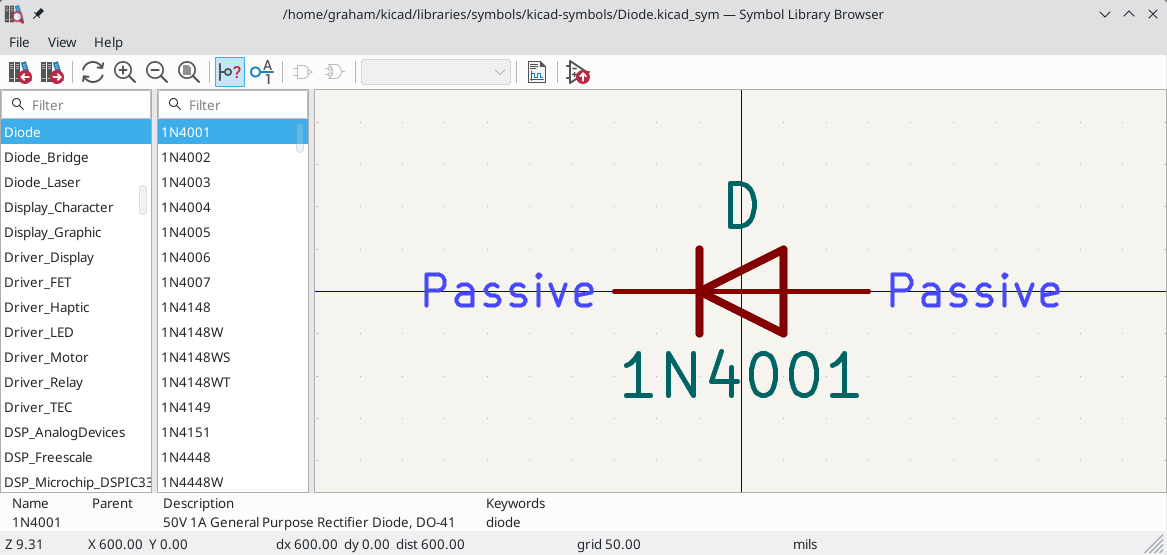
双击符号名称或使用 ![]() 按钮将符号添加到原理图中。
按钮将符号添加到原理图中。
顶部的工具条包含以下命令:
|
Select previous symbol in library. |
|
Select next symbol in library. |
|
Zoom tools. |
|
Toggle display of pin electrical types. |
|
Toggle display of pin numbers. |
|
Select the body style of a symbol with multiple body styles. |
|
Select the unit of a multi-unit symbol. |
|
Open the symbol’s datasheet, if it is defined. |
|
Insert current symbol into the schematic. |
创建和编辑符号
符号是一个元件的在原理图上的表述。一个符号由以下部分组成:
-
图形对象(直线、圆形、圆弧、文字等),决定了符号在原理图中的外观。
-
Pins, which connect to wires in the schematic and correspond to footprint pads in the PCB. Pins have both graphic properties (line, clock, inverted, low level active, etc.) and electrical properties (input, output, bidirectional, etc.) used by the Electrical Rules Check (ERC) tool.
-
字段,如位号、值、PCB 设计的对应封装名称等。
A symbol library is composed of one or more symbols. Generally the symbols are logically grouped by function, type, and/or manufacturer. Each symbol library is a single file with the .kicad_sym extension.
Symbols can be derived from another symbol in the same library. Derived symbols share the basic shape and pin definitions of a base symbol, but can override the base symbol’s metadata. For more information, see the derived symbol section.
符号编辑器概述
KiCad provides a symbol editing tool that allows you to create libraries; add, edit, delete, or transfer symbols between libraries; export symbols to files; and import symbols from files. The Symbol Editor can be launched from the KiCad Project Manager or from the Schematic Editor (Tools → Symbol Editor). You can also open the Symbol Editor from the a symbol in the schematic; in this way you can edit either the library copy or the schematic copy of that symbol in the editor.
| Editing the library version of a symbol will not affect any copies of that symbol that have been added to a schematic until the schematic copy is updated from the library. Conversely, editing the schematic version of a symbol will not affect the library version of a symbol or any other copies of that symbol in a schematic. |
一般来说,设计一个符号的流程包括:
-
定义符号是否由一个或多个单元组成。
-
定义符号是否有替代的主体风格(也称为德摩根代号)。
-
使用直线、矩形、圆形、多边形和文字设计其符号外观。
-
添加引脚,并仔细定义每个引脚的图形元素、名称、编号和电气属性(输入、输出、三态、电源输出等)。
-
Determining if the symbol should be derived from another symbol with the same graphical design and pin definition.
-
添加可选的字段,如 PCB 设计软件使用的封装名称和/或定义其可见性。
-
通过添加描述字符串和数据手册链接来记录该符号,等等。
-
将其保存在所需的库中。
The Symbol Editor main window is shown below. It has three toolbars for quick access to common features and a symbol viewing/editing canvas. Not all commands are available on the toolbars, but all commands are available in the menus.
| You can edit the toolbars' contents in the Toolbar page of the Symbol Editor Preferences. |
In addition to the toolbars, there are collapsible panels for the symbol tree, Properties Manager, and selection filter on the left. The bottom of the window contains a message panel that shows details about the selected object.
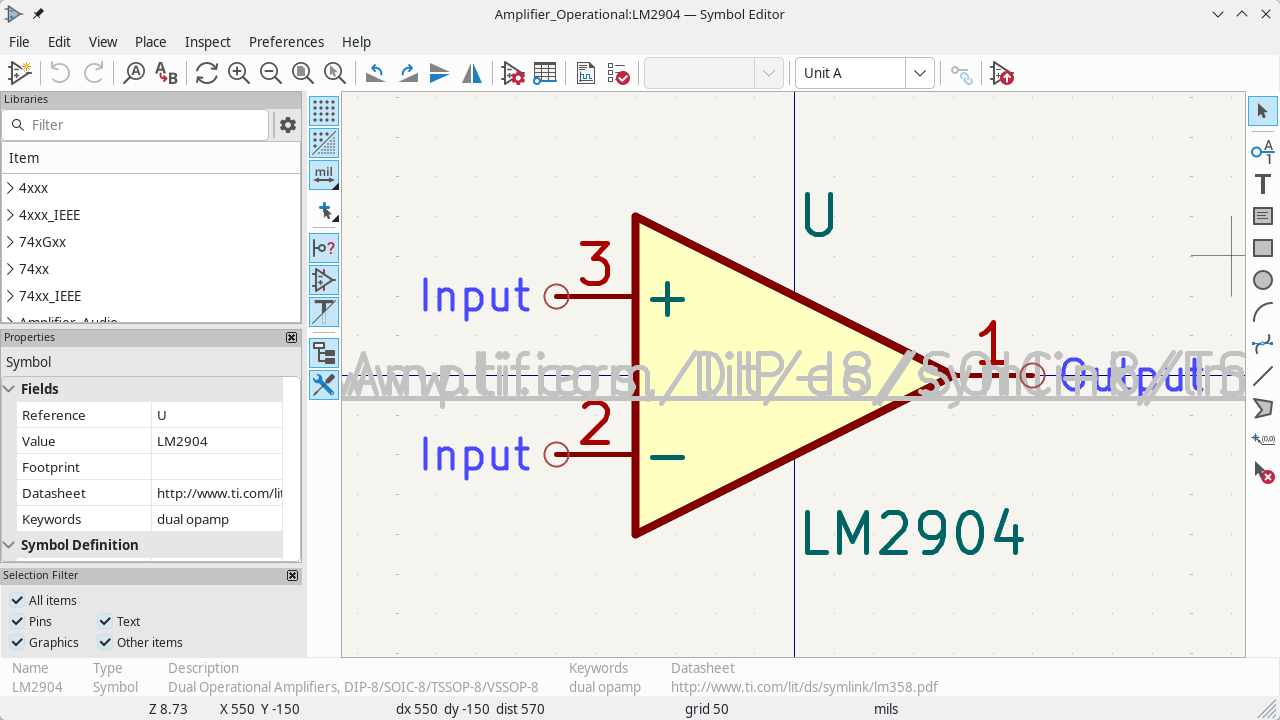
Top toolbar
主工具栏位于主窗口的顶部。工具栏的按钮包括撤销/重做命令、缩放命令、符号属性对话框和单元外观管理控制等。
|
Create a new symbol in the selected library. |
|
Save the currently selected library. All modified symbols in the library will be saved. |
|
Undo last edit. |
|
Redo last undo. |
|
Refresh display. |
|
Zoom in. |
|
Zoom out. |
|
Zoom to fit symbol in display. |
|
Zoom to fit selection. |
|
Rotate counter-clockwise. |
|
Rotate clockwise. |
|
Mirror horizontally. |
|
Mirror vertically. |
|
Edit the current symbol’s properties. |
|
Edit the symbol’s pins in a tabular interface. |
|
Open the symbol’s datasheet, if it is defined. |
|
Run the symbol checker to test the current symbol for design errors. |
|
Select the body style to display. The drop down control will be disabled if the current symbol does not have multiple body styles. |
|
Select the unit of a multi-unit symbol to display. The drop down control will be disabled if the current symbol does not have multiple units. |
|
Enable synchronized pin edit mode. When this mode is enabled, any pin modifications are propagated to all other symbol units. Pin number changes are not propagated. This mode is automatically enabled for symbols with multiple interchangeable units and cannot be enabled for symbols with only one unit. |
|
Insert current symbol into the schematic. |
左侧工具栏显示控制
The left toolbar provides options to change the display of items in the Symbol Editor.
|
Toggle grid visibility on and off. |
|
Toggle item-specific grid overrides on and off. |
|
Set units to inches, mils (0.001 inch), or millimeters. Clicking the button toggles to the next unit, or you can choose a unit directly by expanding the palette (click and hold/drag). |
|
Switches the cursor crosshair between small, fullscreen, and 45-degree-rotated fullscreen. Clicking the button toggles to the next crosshair type, or you can choose a crosshair directly by expanding the palette (click and hold/drag). |
|
Toggle display of pin electrical types. |
|
Toggle display of hidden (invisible) pins. |
|
Toggle display of hidden (invisible) fields. |
|
Toggle display of library and symbol tree. |
|
Toggle display of Properties Manager panel. |
Right toolbar tools
Placement and drawing tools are located in the right toolbar.
|
Select tool. Right-clicking with the select tool opens the context menu for the object under the cursor. Left-clicking with the select tool displays the attributes of the object under the cursor in the message panel at the bottom of the main window. Double-left-clicking with the select tool will open the properties dialog for the object under the cursor. |
|
Pin tool. Left-click to add a new pin. |
|
Graphical text tool. Left-click to add a new graphical text item. |
|
Graphical textbox tool. Left-click to add a new graphical textbox item. |
|
Rectangle tool. Left-click to begin drawing the first corner of a graphical rectangle. Left-click again to place the opposite corner of the rectangle. |
|
Circle tool. Left-click to begin drawing a new graphical circle from the center. Left-click again to define the radius of the circle. |
|
Arc tool. Left-click to begin drawing a new graphical arc item from the first arc end point. Left-click again to define the second arc end point. Adjust the radius by dragging the arc center point. |
|
Bezier curve tool. Left-click to begin drawing a new graphical bezier curve item. First click for the start point, then for the control points and the end point. Adjust the curve by dragging the points. |
|
Connected line tool. Left-click to begin drawing a new graphical line item in the current symbol. Left-click for each additional connected line. Double-left-click to complete the line. |
|
Connected line tool. Left-click to begin drawing a new graphical line item in the current symbol. Left-click for each additional connected line. Double-left-click to complete the line. |
|
Anchor tool. Left-click to set the anchor position of the symbol. |
|
Delete tool. Left-click to delete an object from the current symbol. |
Browsing, modifying, and saving symbols
The ![]() button displays or hides the list of available libraries, which allows you to select an active library. When a new symbol is created, it will be placed in the active library.
button displays or hides the list of available libraries, which allows you to select an active library. When a new symbol is created, it will be placed in the active library.
Clicking on a symbol name opens that symbol in the editor, and hovering the cursor over the name of a symbol displays a preview of the symbol.
| Some symbols are derived from other symbols. Derived symbol names are displayed in italics in the treeview. If a derived symbol is opened, its symbol graphics will not be editable. Its symbol fields will be editable as normal. To edit the graphics of a base symbol and all of its derived symbols, open the base symbol. |
After modification, a symbol can be saved in the current library or a different library. To save the modified symbol in the current library, click the ![]() icon.
icon.
| 保存一个修改过的符号也会保存同一库中所有其他修改过的符号。 |
To save the symbol changes to a new symbol, click File → Save As…. The symbol can be saved in the current library or a different library (including a new library), and a new name can be set for the symbol. Alternatively, you can use File → Save Copy As…, which behaves the same as Save As except that the original symbol remains open rather than switching to the new symbol.
To create a new file containing only the current symbol, click File → Export → Symbol…. This file will be a standard symbol library file which will contain only one symbol. The library will not be added to your library table.
The editor can also open symbols from the schematic. To edit a symbol from the schematic, right click a symbol in the Schematic Editor and select Open in Schematic Editor (Ctrl+E).
Editing and saving the schematic copy of a symbol will only update that symbol in the schematic; it will not update other copies of that symbol in the schematic, and it will not change the original library copy of the symbol. When you open the schematic copy of a symbol, the Schematic Editor displays an info bar that warns you the library copy will not be modified. You can click the link in this info bar to open the library version of the symbol instead, or press Ctrl+Shift+E.
Creating a new symbol library
You can create a new symbol library by clicking File → New Library…. This opens a file browser for you to choose a location and name for the new library. Symbol libraries are saved as a file; the file name is the library name plus the suffix .kicad_sym.
The file browser also lets you choose whether the new library should be added to the global symbol library table or the project symbol library table. Libraries in the global library table will be available to all projects, while libraries in the project library table will only be available in the current project.
| The global and project symbol library tables are managed using Preferences → Manage Symbol Libraries…. This includes deleting and renaming symbol libraries. For more information about managing library tables, see the symbol library table documentation. |
After choosing a name, location, and library table, a new, empty library is created. When you create new symbols, you can save them in this library.
创建一个新符号
To create a new symbol in the current symbol library, click the ![]() button. You will be asked for a number of symbol properties.
button. You will be asked for a number of symbol properties.
-
A symbol name.
-
An optional base symbol to derive the new symbol from. The new symbol will use the base symbol’s graphical shape and pin configuration, but other symbol information can be modified in the derived symbol. The base symbol must be in the same library as the new derived symbol.
-
位号前缀(
U,C,R)。 -
每个符号的单元数,以及这些单元是否可以互换(例如,一个 7400 四路 NAND 符号可以有 4 个单元,每个门一个)。
-
是否需要另一种主体样式(有时被称为 "德-摩根等价")。
-
Whether the symbol is a power symbol. Power symbols appear in the Add Power Symbol dialog in the Schematic editor, make global net connections based on their value, cannot be assigned a footprint, and are excluded from the PCB and bill of materials.
-
该符号是否应从物料清单中排除。
-
该符号是否应从 PCB 中排除。
还有几种图形选项。
-
每个引脚的末端和它的引脚名称之间的偏移。
-
是否应显示引脚编号和引脚名称。
-
引脚名称是否应显示在引脚旁边,或显示在符号主体内的引脚末端。
这些属性以后也可以在符号属性窗口中修改。
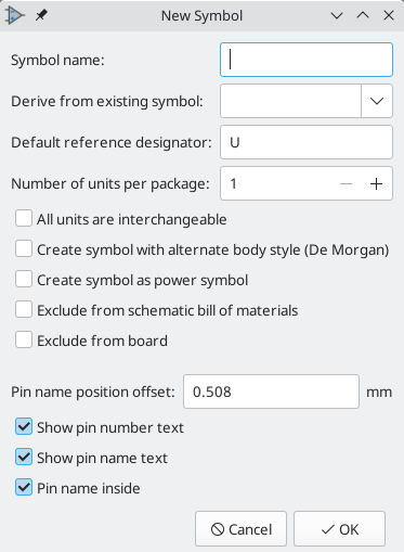
A new symbol will be created in the selected library using the given properties. The new symbol is opened in the editor.
The blue cross in the center is the symbol anchor, which specifies the symbol origin i.e. the coordinates (0, 0). The anchor can be repositioned by selecting the ![]() button and clicking on the new desired anchor position.
button and clicking on the new desired anchor position.
编辑符号属性
Symbols have a number of properties and metadata items that can be defined. These include text fields, attributes that can be set or not (such as Do Not Populate), pin connection settings, and filters for appropriate footprints. These are initially defined in the library copy of the symbol, but they can be modified on a per-instance basis once a symbol is added to a schematic. In other words, two copies of the same symbol in a single schematic can have their properties edited separately.
To change the symbol properties, click on the ![]() button to show the Symbol Properties dialog. You can also double click an empty spot in the editing canvas.
button to show the Symbol Properties dialog. You can also double click an empty spot in the editing canvas.
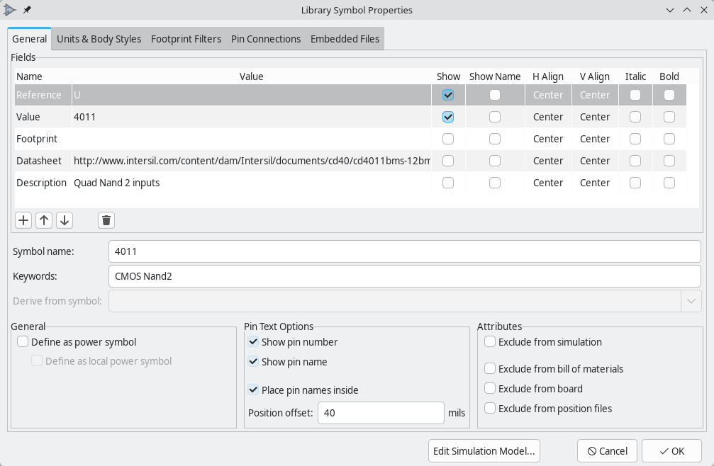
The most important settings are in the General tab. Here you can edit symbol fields as well as many basic properties for the symbol. Other tabs contain options for multiple units and body styles, footprint filters, jumper pins, and embedded files.
Symbol fields are explained in a separate section. The other settings in the general tab are:
-
Symbol name is the symbol’s name in the library. Symbols are identified by a combination of the library and symbol name. In older versions of KiCad, the symbol name was linked to the
Valuefield. This link is removed in KiCad 7.0 and later. -
The keywords should contain additional terms related to the component. Keywords are primarily used, in combination with the symbol name and the
Descriptionfield, for searching for the symbol in the Symbol Chooser and the Symbol Editor. Those three items are also displayed when you select a symbol in the Symbol Chooser. -
Define as power symbol and Define as local power symbol control whether the symbol acts as a power symbol, making connections between otherwise separate nets.
-
The graphic options Show pin number and Show pin name control the visibility of the pin number and pin name text.
-
Place pin names inside controls the pin name position relative to the pin body. The pin names will be displayed inside the symbol outline if the option is checked. In this case the Pin Name Position Offset property defines the shift of the text away from the body end of the pin. A value from
0.02to0.05inches is usually reasonable. -
Exclude from simulation, Exclude from bill of materials, Exclude from board, and Exclude from position files set the default state of these symbol attributes when the symbol is added to the schematic.
下面的例子显示了一个没有勾选 将引脚名称置于内部 选项的符号。注意名称和引脚编号的位置。
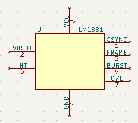
Symbol units and alternate body styles
Symbols can have more than one unit per package, each with different graphics and pin configurations. This is often used for logic gates, opamps, or other components that have multiple subunits within one physical package. Each symbol unit can be placed separately in the schematic, which can make it easier to draw neat schematics.
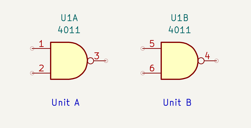
Symbols can also have multiple body styles, which are alternate graphical representations of the same symbol. For example, the symbol for a NAND gate could have one body style showing an ANSI-style AND gate with inverting "bubble" on the output, another body style drawn as an OR gate with inverting "bubbles" on the inputs, and a third body style with an IEC-style rectangular NAND gate symbol.
| Before KiCad 10.0, a maximum of one alternate body style per symbol was possible, and a symbol’s alternate body style was sometimes referred to as a "De Morgan equivalent". Beginning in KiCad 10.0, multiple alternate body styles are possible. |
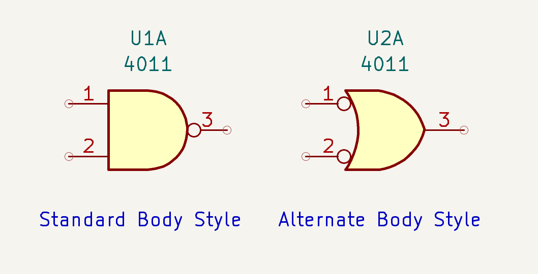
By default, pins are part of a single unit and body style in the symbol. Alternatively, pins can be set as common to all units or common to all body styles. When a pin is common to all units or all body styles, it only needs to be created once, no matter how many units or body styles are used. Graphics and text may also be set as common to all units or body styles, but typically graphics are specific to a single body style so that each body style can have a unique appearance.
The settings for adjusting a symbol’s units and body styles are in the Units & Body Styles tab of the Symbol Properties dialog.
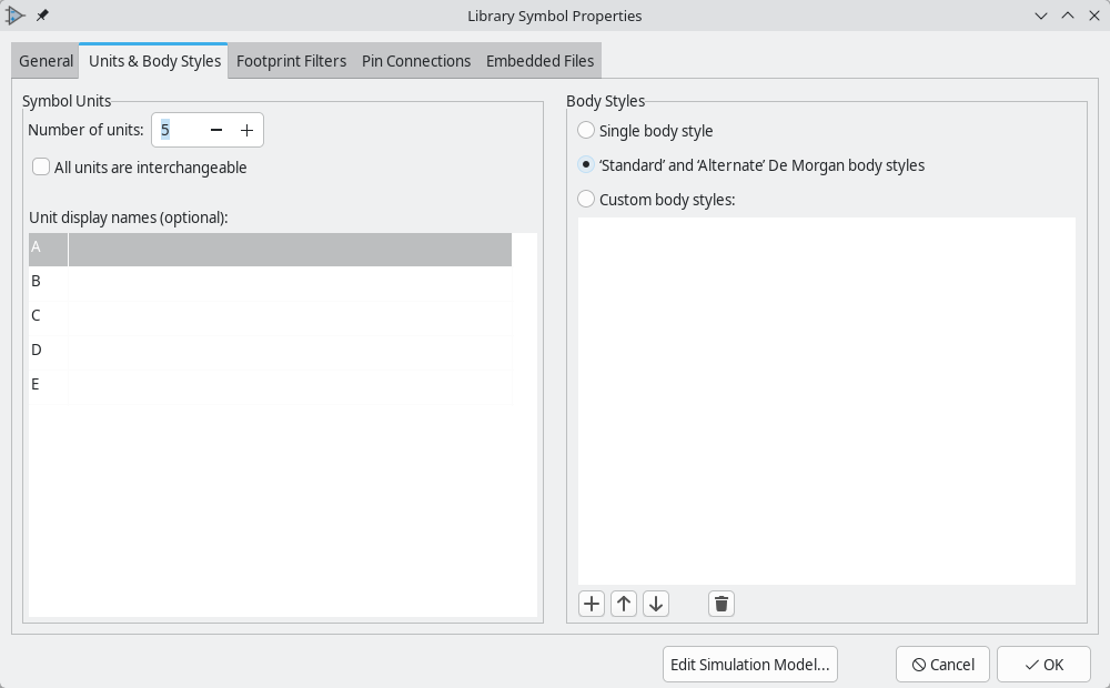
-
Number of Units controls the number of symbol units.
-
All units are interchangeable should be set if all symbol units are equivalent. If all units are interchangeable, you can use the Synchronized Pin Edits mode to quickly make changes to all units.
-
The Unit Display Names table lets you set an optional name for each unit. If you do not configure display names, symbol units are named
Unit A,Unit B, etc. -
The Body Styles options let you select between a single body style, two body styles for traditional "Standard" and "De Morgan" representations of a symbol, and an arbitrary number of custom body styles. If you enable custom body styles, you can set the name for each style.
You can only view and edit one symbol unit and body style at a time in the symbol editor’s editing canvas. Use the  unit selection dropdown to select the unit you wish to edit, and use the
  body style selection dropdown to select a body style.
|
Synchronized Pins Edit Mode can be enabled by clicking the
|
Symbol graphics
Graphical elements create the visual representation of a symbol and contain no electrical connection information. You can draw new graphic shapes using the buttons on the right toolbar. The following types of objects are available:
-
Lines (
 ) and polygons (
 ) defined by start and end points.
 -
Rectangles (
 ) defined by two diagonal corners.
 -
Circles (
 ) defined by the center and radius.
 -
Arcs (
 ) defined by the starting and ending point of the arc and its center.
 -
Graphical text (
 ) and textboxes (
 ), which is automatically oriented to be readable, even when the symbol is mirrored. Note that graphic text items are not the same as symbol fields.
Each graphic item (line, arc, circle, etc.) can be defined as common to all units and/or body styles or specific to a given unit and/or body style.
Element options can be quickly accessed by right-clicking on the element to display the context menu for the selected element. You can also double-left-click on an element to modify its properties, or edit its properties using the Properties Manager panel.
Below is the properties dialog for a polygon element.
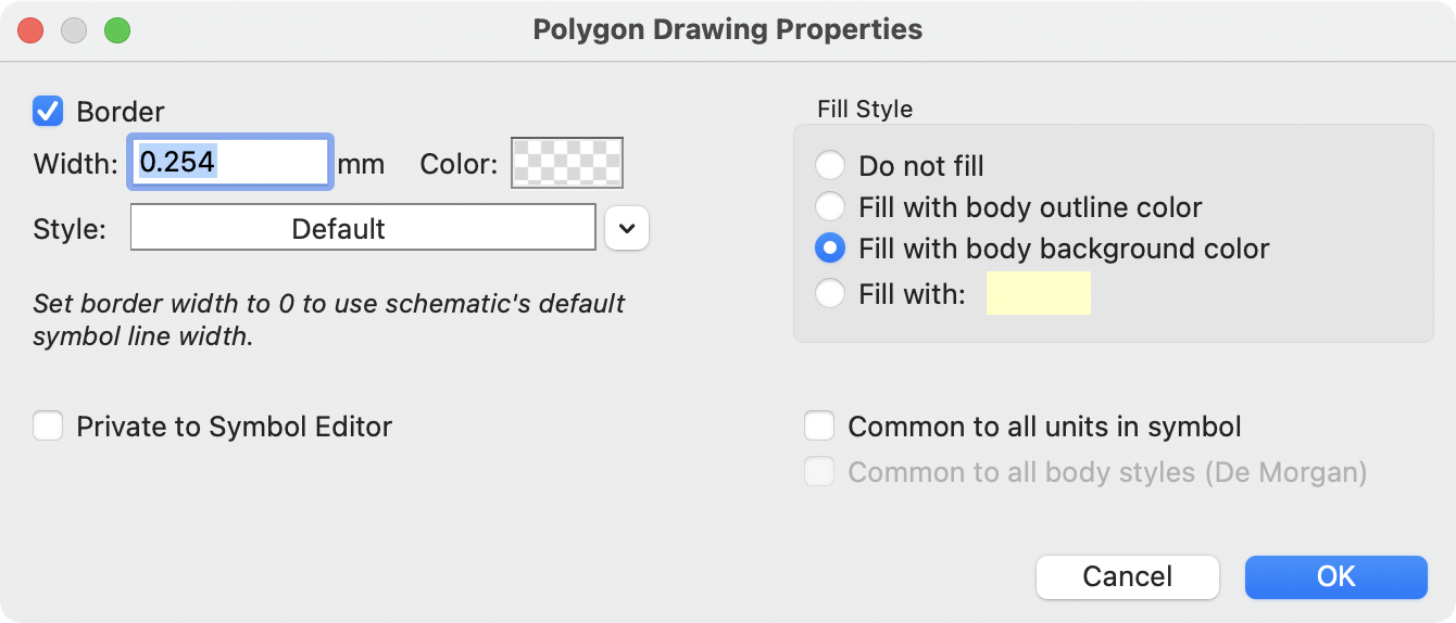
图形元素的属性是:
-
Border determines whether the the shape’s outline should be drawn.
-
Width and color define the line width and color of the border. A border width of
0uses the schematic’s default symbol line width. Style determines the line style of the border (solid, dashed, dotted, etc.). -
Fill Style determines if the shape defined by the graphical element is to be drawn unfilled or filled. The fill color can be the color theme’s body outline color, body background color, or a custom color.
-
Common to all units in symbol determines if the graphical element is drawn for each unit in symbol with more than one unit per package or if the graphical element is only drawn for the current unit.
-
Common to all body styles determines if the graphical element is drawn for each symbolic representation in symbols with an alternate body style or if the graphical element is only drawn for the current body style.
-
Private to Symbol Editor causes the shape to be visible only when the symbol is edited in the Symbol Editor. The shape will be hidden when the symbol is added to a schematic.
Symbol pins
Symbol pins are the parts of a symbol that connect to wires in the schematic. Each symbol pin corresponds to a footprint pad in the PCB, and pins are matched to pads by number, so each pin’s number must match the corresponding pad number in the footprint.
You can create and insert a pin by clicking on the ![]() button. This opens the Pin Properties dialog, then allows you to place the pin in the symbol. After placing a pin, you can edit its properties by reopening its Properties dialog (E or double click on the pin) or by using the Properties Manager.
button. This opens the Pin Properties dialog, then allows you to place the pin in the symbol. After placing a pin, you can edit its properties by reopening its Properties dialog (E or double click on the pin) or by using the Properties Manager.
| You can edit all of a symbol’s pins at once using the Pin Table. This may be a more convenient way to edit pins, especially for symbols with many pins. |
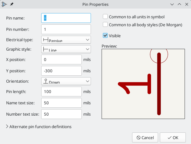
Pins have the following properties:
-
Pin name is an optional name for the pin. Pin names can be displayed as part of the symbol, and if present they are used as part of automatically generated net names for unnamed nets attached to the pin. Pin names cannot contain spaces; any spaces in a pin name are automatically replaced with underscores. To define a pin name with an inverted signal (overbar) use the
~(tilde) character followed by the text to invert in braces. For example,~{FO}Owould display FO O. -
Pin number is a string that uniquely identifies the pin. Symbol pins are matched to footprint pads by pin/pad number, so pin numbers should correspond to pad numbers. Pin numbers are typically unique within a symbol. In addition to numbers, pin numbers can contain letters or symbols. Pin numbers cannot contain spaces; any spaces in a pin number are automatically replaced with underscores.
-
Electrical type describes how the pin behaves electrically, such as input, output, or open collector. Electrical types affect ERC and some other behavior.
-
Graphic style controls the appearance of the pin, such as an inverted pin or a clock input, but does not have any other effects.
-
X position and Y position are the location of the pin relative to the symbol’s anchor.
-
Orientation is the direction the pin extends (left, right, up, or down) relative to its wire attachment point.
-
Pin length is the length of the pin.
-
Name text size and Number text size are the size that the pin name and number, respectively, are displayed at.
-
Common to all units in symbol controls whether the pin is part of all symbol units or only the currently active symbol unit.
-
Common to all body styles controls whether the pin is shown in all body styles or only the currently active body style.
-
Visible controls whether the pin is shown or hidden. Note that hidden power input pins have special behavior.
-
Alternate pin definitions are optional additional combinations of pin name, electrical type, and graphic style that can be selected in the schematic instead of the default pin definition. These can be used, for example, to represent selectable pin functions in a microcontroller.
Pin electrical types
Each pin in a symbol has an electrical type, such as input, output, or tri-state.
选择正确的电气类型对原理图 ERC 工具很重要。 ERC 将检查引脚的连接是否恰当,例如,确保输入引脚被驱动,电源输入从适当的来源接收电源。
You can use the Pin Conflicts Map in the schematic editor to configure which pin types are allowed to connect and which will conflict. The default Pin Conflicts settings are briefly explained below. For more information, see the ERC documentation.
Additionally, some pin types have special behavior outside of ERC. In the router, pads corresponding to a free pin can be connected to copper of any other net without causing a DRC error, and multiple pads corresponding to a single unconnected pin do not need to be connected to each other in the board.
| The pin type that produces the optimal ERC pin conflict checking behavior is not always the same as the pin’s conceptual pin type. When selecting a pin type, you should consider how that type will interact with the pin type of other connected pins and whether that will result in the desired ERC behavior. An example is an analog control pin that generates a current and senses the voltage generated by that current flowing through an external resistor. This pin could be considered an input pin because it senses a voltage provided externally. However, in a schematic this pin will be connected to a resistor pin (passive) and not to an output pin. There shouldn’t be an ERC violation if the pin isn’t connected to an output pin; in fact, there should be an ERC violation if the pin does connect to another output pin, as the pin would be sourcing a current on a net that is already driven. Therefore such a pin should have the Output pin type even though it is sensing a voltage and could be considered an input. |
Pin Type |
描述 |
Input |
A pin which is exclusively an input. The default Pin Conflicts settings allow input pins to connect to most other types of pin. Also, an ERC violation will be produced if an input pin is not driven, i.e. it is not connected to a pin with type output, bidirectional, tristate, power output, or passive. |
Output |
A pin which is exclusively an output. The default Pin Conflicts settings allow output pins to connect to most types of pin that aren’t also outputs. |
Bidirectional |
A pin that can be either an input or an output, such as a microcontroller data bus pin. The default Pin Conflicts settings allow bidirectional pins to connect to most other types of pins, though there are a few more restrictions than with input pins. |
Tri-state |
A three state output pin (high, low, or high impedance). The default Pin Conflicts settings allow tri-state pins to connect to most other types of pins, but warnings are generated when they are connected to most types of output or power pins. |
无源 |
A pin that is not connected to active electronics, for example pins on a resistor or connector. The default Pin Conflicts settings allow passive pins to connect to most other types of pin. |
Free |
A pin that does not electrically affect the operation of the device. These pins typically represent package leads that are not internally connected to the chip. The default Pin Conflicts settings allow free pins to connect to most other types of pin. In the PCB editor, pads corresponding to free pins can be connected to copper of any other net without causing a DRC error. |
Unspecified |
A pin which has an unspecified type. With the default Pin Conflicts settings, ERC generates warnings when unspecified pins are connected to most other types of pins. |
Power input |
A pin that powers the device. The default Pin Conflicts settings allow power input pins to connect to most other pin types. However, power input pins that are not connected to a power output pin generate an ERC violation. Additionally, power input pins that are marked invisible are automatically connected to the net with the same name as the pin. This behavior is supported primarily for legacy projects and is not recommended for new designs. See the Hidden Power Pin section for more information. |
Power output |
A pin that provides power to other pins, such as a regulator output. The default Pin Conflicts settings allow power output pins to connect to most types of input pins, but not output pins. |
Open collector |
An open collector logic output. The default Pin Conflicts settings allow open collector pins to connect to most input pins and other open collector pins, but not to most other types of outputs. |
Open emitter |
An open emitter logic output. The default Pin Conflicts settings allow open collector pins to connect to most input pins and other open emitter pins, but not to most other types of outputs. |
Unconnected |
A pin that should not be connected to anything. ERC does not allow pins of type unconnected to connect to any other type of pin, and ERC will not generate an "unconnected pin" violation when pins of this type are left unconnected. Unconnected pins are not configurable in the ERC Pin Conflicts map. If a footprint has multiple pads corresponding to a single unconnected pin, the pads do not need to be connected to each other in the board. When multiple pins of type unconnected are stacked in a symbol, they are connected to separate nets, whereas stacked pins of other types are connected to the same net. Note that this pin type is different than placing a no connect flag on a pin in the schematic. The unconnected pin type indicates that the pin should never be connected in any schematic, while a no connect flag indicates that the pin is intentionally unconnected in the current schematic. |
Pin stacks
When a symbol has multiple pins that should always be connected to each other, you can choose to draw the symbol so that those pins are stacked. Because the pins are in the exact same location, all pins in the stack are always connected to each other and to any attached wires or labels. As an example, ground (or power) pins are often stacked in symbols where the ground pins should always be connected together.
There are two ways to draw stacked pins in the Symbol Editor; both are equivalent.
-
You can place multiple individual pins in the same location so that they are literally stacked on top of each other. Each pin in the stack corresponds to a physical pin in the package (and to a pad in the footprint). Each pin in the stack has its own pin number. Because only the top pin in the stack is shown, it can be hard to tell which other pins are in the stack. Before KiCad 10.0, stacking multiple pins was the only way to create pin stacks.
-
You can place a single pin and enter multiple numbers in square brackets (
[]) as the pin number. For example, a pin with the pin number given as[1-3]represents pins 1, 2, and 3.[1,2,3]and[1-2,3]also represent the same set of pins. Despite being shown as a single pin, all the pin numbers are displayed. This method was introduced in KiCad 10.0.
Both forms of pin stacks are equivalent and result in the same electrical connections on the PCB. The second method has the advantage of visually showing all of the stack’s pin numbers.
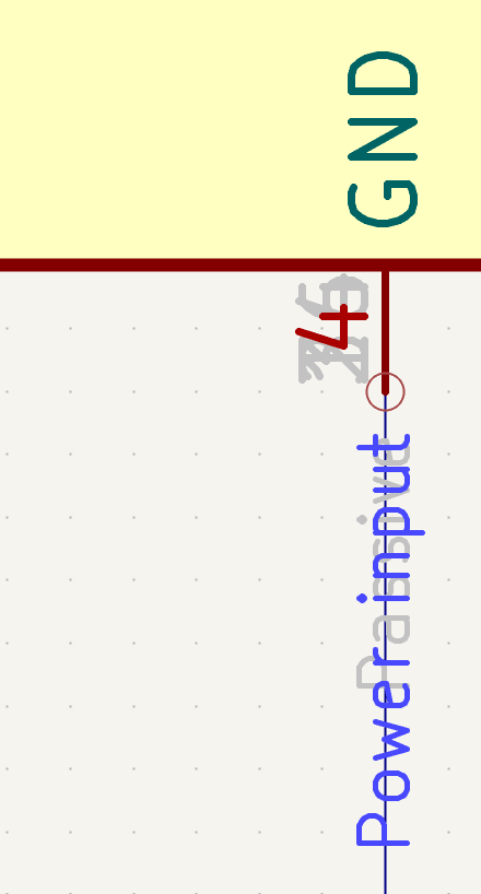
Exploded pin stack (separate pins)
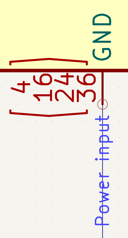
Single pin with multiple pin numbers
You can convert an exploded pin stack (a stack of individual pins) to a single pin with multiple pin numbers by right clicking the pin stack and choosing Convert Stacked Pins. You can do the reverse operation, converting a single pin with multiple pin numbers to a stack of individual pins, by right clicking the pin and choosing Explode Stacked Pin.
When working with exploded pin stacks (a stack of separate pins), there are several considerations to keep in mind.
-
Typically, the top pin in the stack is visible, but the other pins in the stack should be marked as invisible. This has the advantage of avoiding the crowded appearance of multiple pins, their numbers, and their names printed on top of each other, but the disadvantage of not clearly showing that the additional pins exist.
-
The top pin can be set to the most appropriate electrical type, but the other pins should usually be set to the Passive electrical type. This allows ERC to check connections to the pin stack, while avoiding ERC conflicts between pins in the stack. If the pin type is Power Input, it’s especially important to set the hidden pins to Passive because this avoids creating hidden power input pins, which act as global labels.
| Invisible pins with the Power Input type act like global labels. |
Defining pins for multiple units and body styles
Symbols with multiple units and/or graphical representations are particularly problematic when creating and editing pins. Most commonly, pins are specific to each symbol unit (because each unit has a different set of pins) and to each body style (because the form and position is different between the normal body style and the alternate form).
符号库编辑器允许同时创建引脚。默认情况下,对引脚所做的修改是针对一个多单元符号的所有单元,以及对具有替代符号主题样式的两种表示法。 唯一的例外是引脚的图形类型和名称,它们在符号单元和主体样式之间保持无关联。建立这种依赖关系是为了在大多数情况下更容易创建和编辑引脚。这个依赖关系可以通过切换主工具栏上的 ![]() 图标来禁用。这将允许你完全独立地为每个单元和代表创建引脚。
图标来禁用。这将允许你完全独立地为每个单元和代表创建引脚。
引脚可以是共用的,也可以是不同单元所特有的。引脚可以是两个符号主体样式共有的,也可以是每个符号主体特有的。当一个引脚对所有单元都通用时,它只需要绘制一次。引脚可以在引脚属性对话框中设置为通用或特定。
An example is the output pin in the 7400 quad dual input NAND gate. Since there are four units and two symbolic representations, there are eight separate output pins defined in the symbol definition. When creating a new 7400 symbol, unit A of the normal symbolic representation will be shown in the library editor. To edit the pin style in the alternate symbolic representation, it must first be enabled by selecting the alternate representation with the dropdown control. To edit the pin number for each unit, select the appropriate unit using the drop down control.
Alternate pin function definitions
Symbol pins can have alternate pin functions defined for them. Alternate pin functions allow you to select a different name, electrical type, and graphical style for a pin when a symbol has been placed in the schematic. This can be used for pins that have multiple functions, such as microcontroller pins.
Alternate pin functions are added in the Pin Properties dialog as shown below. Each alternate definition contains a pin name, electrical type, and graphic style. This microcontroller pin has all of its peripheral functions defined in the symbol as alternate pin names.
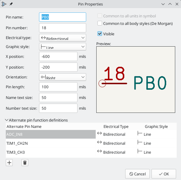
Alternate pin functions are selected in the Schematic Editor once the symbol has been placed in the schematic. For information on using alternate pin functions in the schematic, see the schematic editor symbol documentation.
Pushing pin properties to other pins
你可以通过右击一个引脚,并分别选择 推送引脚长度、推送引脚名称大小 或 推送引脚编号大小,将该引脚的长度、名称大小或数字大小应用于符号中的其他引脚。符号中的所有其他引脚将被更新。
引脚表
Another way to edit pins is to use the Pin Table, which is accessible via the ![]() button. The Pin Table displays all of the pins in the symbol and their properties in a table view, so it is useful for making bulk pin changes.
button. The Pin Table displays all of the pins in the symbol and their properties in a table view, so it is useful for making bulk pin changes.
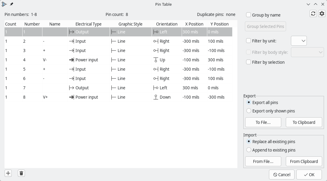
任何引脚属性都可以通过点击相应的单元格进行编辑。可以用 ![]() 和
和 ![]() 图标分别添加和删除引脚。
图标分别添加和删除引脚。
| 通过右键单击标题行并勾选或取消附加列,可以显示或隐藏引脚表的各列。有些列是默认隐藏的。 |
You can edit the same property for multiple pins simultaneously by grouping pins. Pins can be automatically grouped by name with the Group by name checkbox, or you manually group several pins by selecting them and clicking Group Selected Pins. Click the ![]() button to clear the manual grouping. You can also filter the table to only display pins in certain units or body styles, or filter to the pins selected in the symbol editor.
button to clear the manual grouping. You can also filter the table to only display pins in certain units or body styles, or filter to the pins selected in the symbol editor.
If Highlight on cross-probe is enabled in the ![]() menu, pins will be highlighted in the symbol editor when you select them in the pin table.
menu, pins will be highlighted in the symbol editor when you select them in the pin table.
You can also import and export pins from the pin table. This lets you define and edit pins in an external spreadsheet tool. Especially for symbols with many pins, this may be more convenient than editing them within KiCad.
To export pins from the table, click either the To File… or To Clipboard button. The pins are exported in a comma-separated (CSV) format. All columns are exported, even if they are hidden in the table. If Export all pins is selected, all pins in the symbol are included. If Export only shown pins is selected, only the pins shown in the table are included.
To import pins into the table, click either the From File… or From Clipboard button. Data for import needs to be in either comma-separated (CSV) or tab-separated (TSV) format. A header row with column names is required: columns in the imported data are mapped to columns in the pin table by name. Any columns in the imported data that don’t match a column in the pin table will be skipped, and any columns that are missing in the imported data will be filled with default values in the pin table. If Replace all existing pins is selected, the pins in the table are completely replaced by the imported pins. If Append to existing pins is selected, the imported pins are added to the table without modifying or replacing the existing pins.
Symbol fields
Symbols contain multiple fields, which are named values containing information related to the symbol. Fields can be displayed on the schematic or hidden and only shown in the symbol’s properties. Some fields have special meaning to KiCad: Reference and Footprint are both critical for creating a PCB, for example. Other fields may contain information that is important for a design but is not interpreted by KiCad, like pricing or stock information for a part.
Any fields defined in a library symbol will be included in the symbol when it is added to a schematic. You can also add new fields to symbols in the schematic. Whether they are in the library symbol or not, these fields can then be edited on a per-symbol basis in the schematic. They are also transferred to the symbol’s corresponding footprint in the PCB.
| Symbol fields are different than graphic text. In addition to being named, fields can be moved and edited in the schematic, while symbol text can only be edited in the symbol editor. |
All library symbols are defined with five default fields: Reference, Value, Footprint, Datasheet, and Description, which are added whenever a symbol is created. These default fields cannot be deleted. Only the Reference field is required to have a value: the contents of a library symbol’s Reference field is used as the reference designator prefix when the symbol is added to a schematic. In the schematic, the symbol’s Reference field contains the entire reference designator.
如果使用 封装 字段,则包含符号与封装关联。格式是 LIBNAME:FOOTPRINTNAME,其中 LIBNAME 是封装库表中的封装库名称(见 PCB 编辑器手册中的 封装库表部分),FOOTPRINTNAME 是 LIBNAME 库中的封装名称。
The Description field can contain text describing the symbol such as the component function, distinguishing features, and package options. Together with the symbol’s name and keywords, text in this field is used when searching for symbols in the Symbol Chooser or Symbol Editor. Before KiCad version 8.0, this was a dedicated property (like the symbol name and keywords) rather than a symbol field.
Symbols defined in libraries are typically defined with only these five default fields. Additional fields such as vendor, part number, unit cost, etc. can be added to library symbols but generally this is done in the schematic editor so the additional fields can be added to every symbol in the schematic, not just all symbols of one type.
| 创建额外的空符号字段的一种便捷方法是使用定义字段名称模板。字段名称模板定义空字段,当每个符号插入原理图时,这些字段会被添加到每个符号中。字段名称模板可以在原理图编辑器首选项中全局定义(针对所有原理图),也可以在原理图设置对话框中局部定义(针对每个工程)。 |
| 如果你想在符号字段中管理大量的元件数据,可以考虑使用数据库关联库。 |
要编辑一个现有的符号字段,请双击该字段,选择它或悬停并按 E,或右击字段文本并选择 属性…。
To add new fields, delete optional fields, or edit existing fields, use the ![]() icon on the main tool bar to open the Symbol Properties dialog. Fields can be arbitrarily named, but names starting with
icon on the main tool bar to open the Symbol Properties dialog. Fields can be arbitrarily named, but names starting with ki_, e.g. ki_description, are reserved by KiCad and should not be used for user fields.
Fields have a number of properties, each of which is shown as a column in the properties grid. Not all columns are shown by default; columns can be shown or hidden by right clicking on the grid header and selecting or deselecting columns from the menu.
| You can edit fields for many symbols at once using the Symbol Fields Table, which lets you edit the fields of all symbols in the same library at once. |
封装筛选器
封装筛选器标签用于定义哪些封装适合与符号一起使用。筛选器可以在封装分配工具中使用,以便只显示每个符号合适的封装。
可以定义多个封装筛选器。符合任何一个筛选器的封装将被显示;如果没有定义筛选器,那么所有的封装都将被显示。
筛选器可以使用通配符。* 匹配任何数量的字符,包括零,而 ? 匹配零或一个字符。例如,SOIC-* 将匹配 SOIC-8_3.9x4.9mm_P1.27mm 封装以及任何其他以 SOIC- 开头的封装。筛选器 SOT?23 匹配 SOT23 以及 SOT-23。
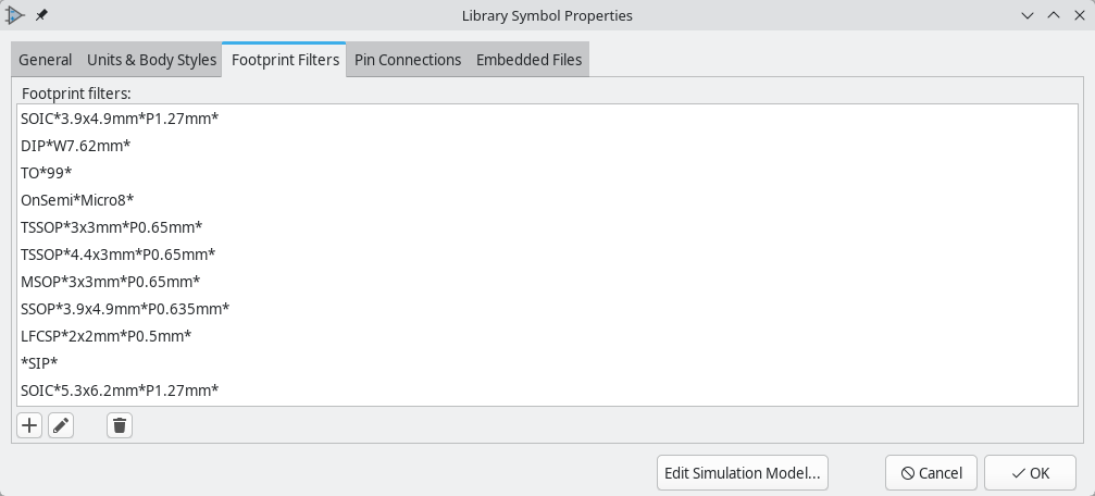
Jumper pins
You can configure a symbol to jumper some or all of its pins internally. Any jumpered pins will always have the same net; they are considered shorted together, even if they are not explicitly connected together in the schematic and PCB.
Symbols with jumper pins represent components that internally short together multiple pins. Examples of such components are wire jumpers, connectors with multiple connected shield pins, and switches with multiple shorted pins on each side of the switch.
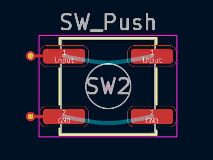
A footprint without jumpered pads. The ratsnest shows missing connections between same-numbered pads.
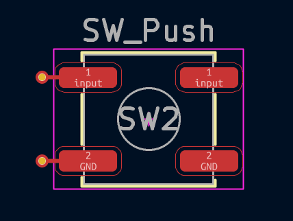
The same footprint in the same circuit with same-number pads jumpered (internally connected by the component). PCB connections between the same-numbered pads are no longer required.
Because KiCad considers the jumpered pins to be shorted by the component, you only need to connect to one of the shorted pins in the schematic and PCB.
| Jumper pins are different than net ties. A net tie allows copper to bridge two different nets, and each pad in the net tie has a different net. With jumper pins, each pin has the same net, and the electrical connection between jumper pins is assumed to be off-board in the attached component. |
You can configure jumper pins in the Pin Connections tab of a symbol’s Properties.
When the All pins with duplicate numbers are jumpers setting is enabled, all pins (and pads in the linked footprint) will be jumpered to the other pins with the same number. For example, all pins numbered 1 will be considered connected to each other.
You can also configure jumper pin groups for pins that don’t have the same number by adding Explicit pin jumper groups with the ![]() button. Enter multiple pin numbers separated by spaces or commas. A pin jumper group with the text
button. Enter multiple pin numbers separated by spaces or commas. A pin jumper group with the text 1 2 or 1, 2 will jumper together pins 1 and 2. A group with 3 4 5 or 3, 4, 5 will jumper together pins 3, 4, and 5.
| Like many other symbol properties, a symbol’s jumper pin settings are transferred to the linked footprint. You can also configure a footprint’s jumper pads using the Footprint Editor. |
Embedding files
External files can be embedded within a symbol. Embedding a file stores a copy of the file inside the symbol. The symbol can then refer to the embedded copy of the file instead of the external file, which makes the symbol more portable as it doesn’t rely on an external file, although the symbol library’s filesize is increased as a result. In symbols this is especially useful for embedding datasheets and SPICE models.
In the symbol editor, you can embed files into library symbols in the Embedded Files tab of a symbol’s properies.
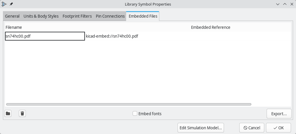
| You can add a datasheet, or a SPICE model, to a symbol and embed it in one step. To do so, browse for a datasheet (in the Symbol Properties dialog) or a SPICE model (in the SPICE Model Editor) and enable the Embed File checkbox in the file browser while choosing a file. This embeds the file and automatically uses the embedded reference as the file path instead of the path to the external file. |
Files embedded in a symbol are deduplicated when the symbol is added to a schematic: if a file is embedded in a symbol, and multiple instances of that symbol are added to the schematic, only one copy of the file will be embedded, and all of the schematic instances will refer to the same embedded file.
When a symbol is derived from a symbol with embedded files, the derived symbol can access both its own embedded files and the files embedded in the parent symbol. Files embedded in a symbol cannot be referred to in the parent schematic outside of the symbol.
File embedding is explained in more detail in the Schematic Setup documentation.
Creating power symbols
Power symbols are symbols that are used to label a wire as part of a global power net, like VCC or GND. The power symbol’s Value field determines the net label. The behavior of power symbols is described in the electrical connections section. Power symbols are handled and created the same way as normal symbols, but there are several additional considerations described below.
将电源符号放在一个专门的库中可能是有用的。KiCad 的符号库将电源符号放在 power 库中,用户可以创建库来存储自己的电源符号。如果在符号的属性中勾选了 定义为电源符号 框,该符号就会出现在原理图编辑器的 添加电源符号 对话框中,以便于访问。
Power symbols consist of a single pin of type Power Input. They must also have the Define as power symbol property checked.
In previous versions of KiCad, a power symbol’s pin needed to be both a
power input pin and invisible, and the pin’s name determined the name of
the net that the power symbol connected with. Beginning in KiCad version
8, the pin in a power symbol does not need to be invisible, and the net is
determined by the power symbol’s Value field.
|
下面是一个 GND 电源符号的例子。
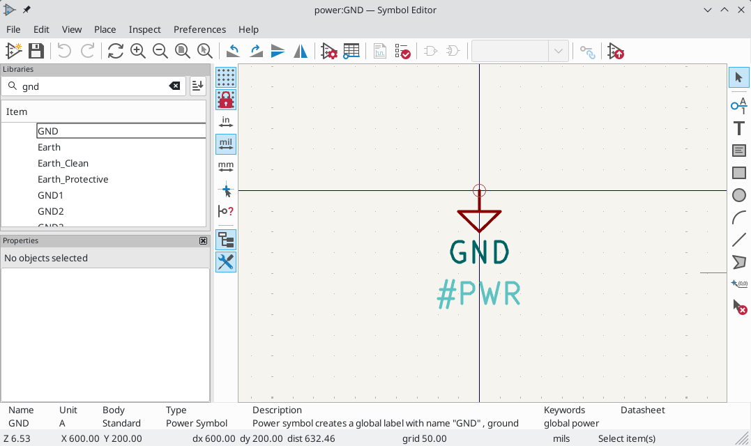
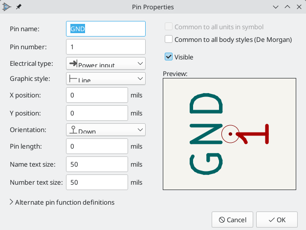
要创建一个电源符号,请使用以下步骤:
-
Add a pin of type Power input. Make the pin number
1, the length0, set the graphic style to Line, and make the pin visible. The pin number, name, length, and line style do not matter electrically. -
Place the pin on the symbol anchor. This is not required but makes it easier to place the power symbol in the schematic.
-
使用形状工具来绘制符号图形。
-
Set the symbol value to the desired net name. The symbol value is electrically important: it determines the symbol’s connected net name. This field can be changed later, after the symbol has been placed in the schematic, which will change which net the symbol connects to.
-
Check the Define as power symbol box in Symbol Properties window. This makes the symbol appear in the Add Power Symbol dialog, prevents the symbol from being assigned a footprint, and excludes the symbol from the board, BOM, and netlists.
-
Also deselect the Show pin number and Show pin name options in the Symbol Properties window. This is not necessary but improves the symbol’s appearance.
-
设置符号的位号并取消勾选 显示 框。位号第一个字符应为
#,后续文本并不重要。对于上面所示的电源符号,位号可以是#GND。位号以#开头的符号不会被添加到 PCB 上,不包括在物料清单的输出或网表中,也不会在封装分配工具中分配一个封装。如果一个电源符号的位号不是以\#开头,当运行批注或封装分配工具时,该符号会被自动插入到符号表中。
An easier method to create a new power symbol is to use another symbol as a starting point.
Creating derived symbols
Symbols can be derived from another symbol in the same library. Derived symbols share the base symbol’s graphical shape and pin definitions, but can override the base symbol’s metadata (value, footprint, datasheet, other fields, description, footprint filters, etc.). Any user-defined fields from the base symbol that are not overridden by the derived symbol are directly inherited.
Derived symbols can be used to define symbols that are similar to a base part. For example, 74LS00, 74HC00, and 7437 symbols could all be derived from a 7400 symbol, because they are all quad NAND gates with the same pinout.
| In previous versions of KiCad, derived symbols were referred to as aliases. |
To create a derived symbol, click the ![]() button. This will create a new symbol in the active symbol library.
button. This will create a new symbol in the active symbol library.
| The derived symbol must be created in the same library as the base symbol. |
Choose a name for the symbol in the Symbol name field, and choose a base symbol from the Derive from existing symbol dropdown.
| As a shortcut for choosing a base symbol for a new derived symbol, you can right click an existing symbol in the library tree and choose Derive from existing symbol…. This opens the New Symbol dialog and preselects the existing symbol as the base symbol. |
When you are creating a derived symbol, most options in this dialog are disabled because the settings are taken from the base symbol. Several options are only applicable to derived symbols, however:
-
Keep linked datasheet: if enabled, the value of the
Datasheetfield from the base symbol is also used in the derived symbol. If not enabled, theDatasheetfield is empty in the derived symbol. -
Keep linked footprint: if enabled, the value of the
Footprintfield from the base symbol is also used in the derived symbol. If not enabled, theFootprintfield is empty in the derived symbol. -
Transfer user-defined fields: if enabled, each user-defined field in the base symbol will also be created as an empty field in the derived symbol. If this option is not selected, the derived symbol automatically inherits the fields and their values from the base symbol.
-
Keep content of user-defined fields: if enabled, the value of each user-defined field in the base symbol will also be set in the derived symbol.
When you click OK, a new derived symbol will be created in the active library.
The derived symbol has the same graphics and pins as the base symbol; therefore, its graphics and pins are not editable. You can only edit the graphics and pins of a derived symbol by editing its base symbol; this will affect the base symbol and any other symbols that are derived from it.
Derived symbols inherit all user-defined fields from the base symbol. This means that derived symbols automatically have all the user-defined fields (and their values) from the base symbol. Inherited fields are displayed in italics to show that they are inherited from the base symbol. You can override an inherited field by giving the field a different value in the derived symbol.
Derived symbols are required to be in the same symbol library as their base symbol. If you perform a Save As on a derived symbol to move it into a new library, the base symbol will also be saved in the new library. To save a derived symbol into a new library without its base symbol, you can flatten the derived symbol.
Flattening derived symbols
You can convert an existing derived symbol into a fully-defined base symbol by right clicking the derived symbol in the library tree and choosing Flatten Symbol. This breaks the derived relationship between the derived symbol and its base symbol. After flattening, all of the graphics, pin definitions, fields, and other metadata are fully defined in the formerly-derived symbol, but are otherwise identical to what they were before the symbol was flattened.
| Derived symbols must be in the same library as their base symbol. Flattening a derived symbol allows the formerly-derived symbol to be moved to a different library. |
You can also flatten derived symbols while performing a Save As operation. Ordinarily, performing a Save As on a derived symbol maintains the existing derived relationship between the derived symbol and its base symbol: the newly saved symbol is still derived from the original base symbol. But if the Flatten/remove symbol inheritance option is checked in the Save As dialog, the derived symbol will be saved as a base symbol.
Bulk editing symbol fields
The Symbol Fields Table allows you to view and modify field values for all symbols in a library using a spreadsheet interface. This is similar to the Symbol Fields Table in the Schematic Editor, but it contains the fields for all symbols in a given library rather than all symbols in a schematic.
You can open the Symbol Fields Table by right clicking on a symbol in the Library Tree panel and choosing Bulk Edit Symbol Fields…. This opens the Symbol Fields Table to edit the fields of all symbols in the same library.
If the symbol is derived or has other symbols that derive from it, you can alternatively choose Bulk Edit Related Symbol Fields…. This also opens the Symbol Fields Table, but shows the fields for the base symbol and all symbols that derive from it.
When the dialog is open, you can switch between editing the whole library’s symbols and just related symbols using the dropdown menu at the top of the window.
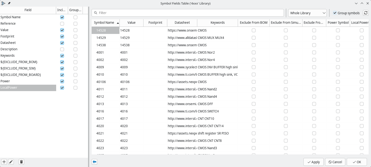
The main table has a row for each symbol and a column for each field. Each cell is editable. Symbol attributes (Exclude From BOM, Exclude From Simulation, Exclude From Board, Power, and Local Power) are shown as checkboxes.
The left pane contains a list of all available symbol fields and attributes. You can add or remove any symbol field from the main table on using the Include checkboxes (fields can also be shown or hidden by right-clicking on the header of the main table). New symbol fields can be added using the ![]() button; a field with that name will be added to every symbol. To rename the field, which changes the field name in all symbols, use the
button; a field with that name will be added to every symbol. To rename the field, which changes the field name in all symbols, use the ![]() button. The
button. The ![]() button deletes the field from all symbols. You can collapse this panel by clicking the
button deletes the field from all symbols. You can collapse this panel by clicking the ![]() button.
button.
Similar symbols can optionally be grouped by any symbol field using the Group By checkboxes. Symbols are grouped into a single row in the table if all of their Group By fields are identical. The grouped row can be expanded to show the individual symbols by clicking the arrow at the left of the row. The Group symbols checkbox enables or disables symbol grouping, and the ![]() button recalculates groupings.
button recalculates groupings.
Symbols can be filtered by symbol name using the Filter textbox at the top. The filter supports wildcards: * matches any number of any characters, including none, and ? matches any single character.
Checking symbols
符号编辑器可以检查符号中的常见问题。使用顶部工具栏上的 ![]() 按钮运行符号检查器。
按钮运行符号检查器。
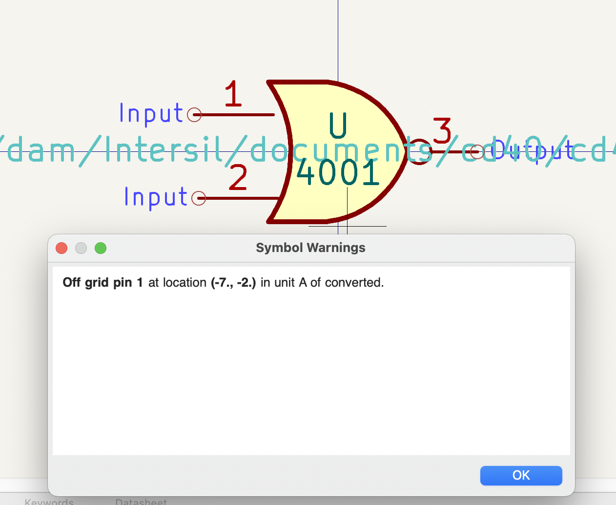
符号检查器检查的是:
-
Pins that are off-grid (pins are considered off grid if their position is not a multiple of the current symbol editor grid. It is strongly recommended to use a 50 mil grid for symbol pins)
-
Pins that are duplicated
-
Issues with graphical shapes, such as zero-sized shapes
-
非法的位号前缀:位号前缀不能用数字或
? -
设计不正确的《电源符号,电源符号》。电源符号应该有:
-
单个引脚
-
没有备用的主体样式
-
单个引脚,其类型为电源输出(见《电源标记,电源标记》),或可见且类型为电源输入(见《电源符号,电源符号》)。
-
-
在非电源符号中,出现了《隐藏的电源输入引脚,隐藏的电源输入引脚》:这将产生隐形的连接,不推荐使用
| In previous versions of KiCad, power symbols required an invisible power input pin so that they would make a global connection. In KiCad 8, the power input pin does not need to be invisible. Therefore the symbol checker will report if invisible power input pins are detected. |
Importing symbols
You can import symbols from an external KiCad library into one of your symbol libraries using File → Import → Symbol…. The source library does not have to be part of your library configuration, but the destination must be a loaded library.
| If you a KiCad symbol from the internet, importing it is a good way to add it to your libraries. |
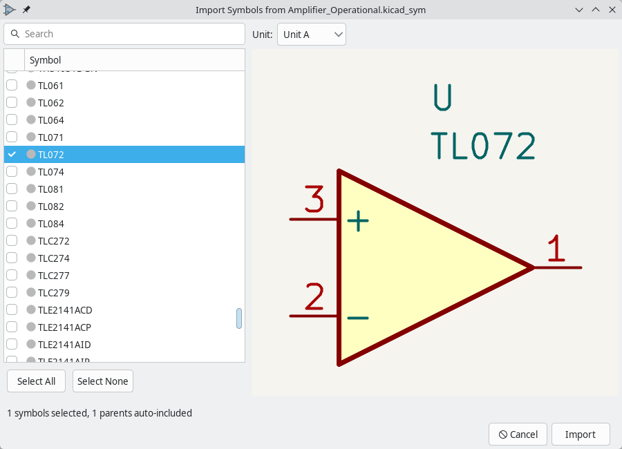
When you start the symbol importer, you are first asked to browse to a library that contains the symbol(s) you want to import. The destination library is the library that is active in the Symbol Editor.
Once you select a source library, all of the symbols in that library are listed. Clicking a symbol in the list shows it in the preview canvas. Any symbols that are selected using the checkboxes next to their names are imported when you click the Import button.
Derived symbols are indicated with a circle in front of their names. Derived symbols cannot be imported by themselves; when you import a derived symbol, the base symbol is automatically imported as well.
| If the source library is already part of your library configuration, an easier way to transfer a symbol from one library to another is to use File → Save As… (or Save Copy As…). |
Importing schematics from other applications
KiCad can import complete schematics saved in several third-party EDA tool formats, converting them to KiCad’s native format in a single step. This allows you to migrate existing designs without having to recreate them from scratch.
Importing a schematic replaces the current schematic with the contents of the imported
file. It does not merge the foreign schematic into an existing KiCad design. After
import, save the schematic using File → Save to create a KiCad .kicad_sch file.
|
How to import a schematic
To import a schematic from a supported third-party format, use File → Import → Non-KiCad Schematic….
An "Import Schematic" file dialog will open. The dialog presents an "All supported formats" filter that includes all importable file types, as well as individual format filters. Select the desired source file and click Open.
KiCad reads the foreign file, converts it to KiCad format, and loads the result into the schematic editor. If the importer encounters any issues during conversion, a report dialog will appear listing warnings and unsupported features.
| If you open a file using File → Open… and the file is not a KiCad schematic, the Schematic Editor will display a message directing you to use File → Import → Non-KiCad Schematic… instead. |
Supported formats
KiCad supports importing schematics from the following EDA tools:
| Source EDA Tool | File Extension(s) | Notes |
|---|---|---|
Altium Designer |
|
Multi-sheet designs are supported; each |
Eagle (Autodesk) |
|
Eagle version 6.x and later (XML format). |
LTspice |
|
LTspice schematic and simulation files. |
PADS Logic |
|
PADS Logic ASCII export format. |
CADSTAR Schematic Archive |
|
Zuken CADSTAR schematic archive files. |
gEDA / Lepton EDA |
|
gEDA gschem and Lepton EDA schematic files. |
EasyEDA (JLCEDA) Standard |
|
EasyEDA Standard edition JSON export. |
EasyEDA (JLCEDA) Professional |
|
EasyEDA Professional edition project files. |
The Eagle .sch extension and the gEDA .sch extension are both used by their
respective tools. KiCad identifies the correct format automatically based on the
file contents.
|
The PADS Logic .asc extension is shared with LTspice. KiCad inspects the file
header to determine which format applies.
|
Format-specific notes
Altium Designer
KiCad imports Altium Designer schematic files (.SchDoc). Altium projects can contain multiple sheets, each saved as a separate .SchDoc file. When you import one sheet, KiCad will also attempt to load the other sheets referenced by that project, reconstructing the sheet hierarchy.
Symbols found in the source file are placed into a generated symbol library that is saved alongside the imported schematic.
If you have a complete Altium project (.PrjPcb) with both schematic and PCB files,
the KiCad Project Manager can import both in a single step. Use File →
Import Non-KiCad Project… → Altium Project… and select the .PrjPcb
file. The .SchDoc import described here is for schematic files imported on their
own.
|
Eagle (Autodesk)
KiCad imports Eagle XML schematic files (.sch), which are the format produced by Eagle version 6.x and later. Eagle schematics store all sheets in a single file.
Symbols are extracted from the embedded Eagle libraries and placed into a generated KiCad symbol library.
| Binary Eagle files created by versions earlier than 6.x are not supported. Open the file in Eagle first and re-save it to convert to the XML format before importing. |
LTspice
KiCad imports LTspice schematic files (.asc). These are the simulation schematics created by LTspice, which uses its own symbol library and netlist conventions.
After import, the schematic will reflect the circuit topology from LTspice, but simulation directives and LTspice-specific elements such as SPICE parameters and behavioral sources may not convert fully. Review the imported schematic and the KiCad SPICE simulator documentation before attempting to run simulations on an imported LTspice design.
PADS Logic
KiCad imports PADS Logic schematic files (.asc or .txt). These are the ASCII text exports produced by the PADS Logic schematic editor. To generate this file from PADS Logic, use File → Export and select the ASCII format.
CADSTAR Schematic Archive
KiCad imports CADSTAR Schematic Archive files (.csa) from Zuken’s CADSTAR tool.
In addition to full schematic import, KiCad can use CADSTAR Parts Library files (.lib) as read-only symbol libraries through the Symbol Library Manager.
gEDA / Lepton EDA
KiCad imports gEDA gschem and Lepton EDA schematic files (.sch). These are ASCII text files produced by the gEDA suite or its fork, Lepton EDA.
Symbols in gEDA schematics reference external .sym files from the gEDA system symbol library. KiCad will search standard gEDA library locations for these symbol files during import. Symbols that cannot be found are replaced with a fallback rectangular symbol. Hierarchical sheets are supported; KiCad will recursively import sub-schematics referenced by source= attributes on component instances.
EasyEDA (JLCEDA) Standard
KiCad imports EasyEDA Standard edition schematic files (.json). To obtain a file for import, export your design from EasyEDA using the Export EasyEDA option, which produces a JSON file.
Symbols are extracted from the embedded library data within the JSON file and placed into a generated KiCad symbol library.
EasyEDA (JLCEDA) Professional
KiCad imports EasyEDA Professional edition project files (.epro or .zip).
For projects containing multiple schematics, KiCad will present a project chooser dialog so you can select which schematic within the project to import.
After importing
After importing a schematic from a third-party tool, review the result and perform any necessary cleanup:
-
Save the schematic: Use File → Save to save the imported design as a KiCad
.kicad_schfile. The file will be placed in the current project directory with the project name. -
Run the Electrical Rules Check (ERC): Select Inspect → Electrical Rules Checker to identify any connectivity or symbol issues introduced during import.
-
Review the import report: If the importer produced warnings, the report dialog will have been shown automatically. Review any warnings about unsupported features or items that could not be converted.
-
Remap symbols: Imported symbols are stored in a generated library created alongside the schematic. If you want to use KiCad standard library symbols instead, use Tools → Edit Symbol Fields to reassign symbols to your preferred library. The symbol remapping tool may also be useful.
-
Assign footprints: Third-party schematics rarely use KiCad footprint references. Use Tools → Assign Footprints to link each symbol to an appropriate KiCad footprint before proceeding to board layout.
-
Check the drawing sheet: Imported schematics do not carry a KiCad drawing sheet (title block). The schematic editor will use an empty drawing sheet after import. To add a title block, open File → Page Settings and choose a drawing sheet template.
Design blocks
Design blocks are a design-reuse feature that lets you save a portion of a schematic (and optionally a corresponding PCB layout) as a named, reusable fragment stored in a design block library. You can instantiate a design block any number of times within the same project or across different projects. Design blocks are organized in libraries in the same way that symbols and footprints are organized in their respective libraries.
A single design block can contain a schematic fragment, a PCB layout fragment, or both. When you place a schematic design block, the saved schematic fragment is inserted into the current schematic sheet or into a new hierarchical subsheet. If the design block also contains a layout fragment, you can later apply that layout to the footprints that were placed as a result of the schematic fragment. This makes design blocks well suited for circuits that appear repeatedly across projects, such as power supply subcircuits, filter networks, protection circuits, and interface conditioning stages.
Typically, design blocks are created first as a schematic fragment, with the layout added later once the circuit has been placed and routed on a board. Reusing layout fragments in design blocks is covered in the PCB Editor manual.
Design block concepts
Two ways to place a design block
When you place a design block into a schematic you choose between two fundamentally different placement modes:
Place inline (no sheet): The contents of the design block are inserted directly into the current schematic sheet alongside all other schematic objects. The content becomes part of the current sheet and can be edited in place.
Place as sheet: The contents of the design block are placed into a new hierarchical subsheet. The current schematic sheet receives a hierarchical sheet symbol whose contents are the design block’s schematic. Placing as a sheet is useful when the design block represents a logically distinct functional block, when you want the design block contents to be visually separate from the parent schematic, or when you plan to reuse the same sheet multiple times as a repeated hierarchical sheet. Default fields defined in the design block’s properties are applied as hierarchical sheet fields when placing as a sheet.
In either mode, also enable the Place as group option to wrap the placed content in a group with a library link. Without a group, features including saving changes back to the library, placing additional linked instances, and applying the stored layout to the corresponding footprints in the PCB editor are not available. The Place as group option works with both placement modes: when enabled alongside Place as sheet, a group wrapping the sheet symbol is added to the parent schematic.
| Design blocks do not support nested hierarchical sheets. If the sheet you are saving as a design block contains hierarchical sheet symbols (subsheets), the save operation will be rejected. |
The library link
When a design block is placed as a group, the group stores a library link in the format <library>:<block> — for example, analog_filters:sallen_key_lowpass. This link connects the placed instance to its source in the library and enables the following operations:
-
Save to Linked Design Block — push edits made to the placed group back to the library, updating the stored design block schematic.
-
Place Linked Design Block — place another instance of the same design block as a new linked group, without reopening the Design Blocks panel.
-
Apply Design Block Layout — in the PCB editor, apply the layout stored in the linked design block to the group of footprints corresponding to this design block instance. As an alternative, the multichannel tool can replicate a manually completed layout from one group to another without requiring a stored layout fragment in the design block.
A group that does not have a library link cannot use any of these operations. If you manually grouped the contents of a design block without using the Design Blocks panel, you can add the library link retroactively in the group’s properties dialog (see Setting a library link manually).
Setting a library link manually
If you have a group in your schematic that contains the same content as an existing design block but the group does not have a library link, you can add the link without re-placing the design block:
-
Select the group and open its properties (right click → Group Properties…, or press E with the group selected).
-
In the Library link field, enter the design block identifier in the format
<library>:<block>. For example,power_circuits:ldo_3v3. -
Click OK.
The group will now behave as a linked group and all library-linked operations will be available.
If you want the design block’s schematic contents to also be grouped in the PCB, either for organizational purposes or so you can apply a design block layout, use the Update PCB from Schematic tool with the Group footprints based on symbol groups option enabled.
Design block library structure
Design block libraries are stored as directories on the filesystem. The directory structure has two levels of nesting:
-
The library itself is a directory whose name ends with
.kicad_blocks(for example,my_power_circuits.kicad_blocks). -
Each design block within the library is a subdirectory inside the library directory, with the suffix
.kicad_block(for example,ldo_3v3.kicad_block). -
Inside each design block directory, KiCad stores:
-
A schematic file (
<block_name>.kicad_sch) — present if the design block contains a schematic fragment. -
A board file (
<block_name>.kicad_pcb) — present if the design block contains a layout fragment. -
A metadata file (
<block_name>.json) — always present; stores the design block’s description, keywords, and default fields.
-
Because libraries and design blocks are plain filesystem directories, they can be managed with ordinary file manager tools, version control systems, or shared over a network filesystem. The library tables (see below) must be updated if library directories are moved or renamed outside of KiCad.
Global and project library tables
As with symbol and footprint libraries, design block libraries are registered in library tables before KiCad can use them. There are two library tables:
-
The global design block library table lists libraries that are available in every KiCad project. The global table is shared across all projects on the same machine.
-
The project design block library table lists libraries that are available only in the current project. The project table is stored alongside the project files.
Both tables are managed through Preferences → Manage Design Block Libraries…. The dialog behaves identically to the symbol and footprint library table dialogs. See the symbol library table documentation for a full description of the library table interface.
The Design Blocks panel
To use schematic design blocks, first show the Design Blocks panel by clicking View → Panels → Design Blocks. This opens a docked panel on the right side of the schematic editor. To close the panel, use the same menu entry again, click the close button in the top right of the panel, or right click in the panel and choose Hide Library Tree.
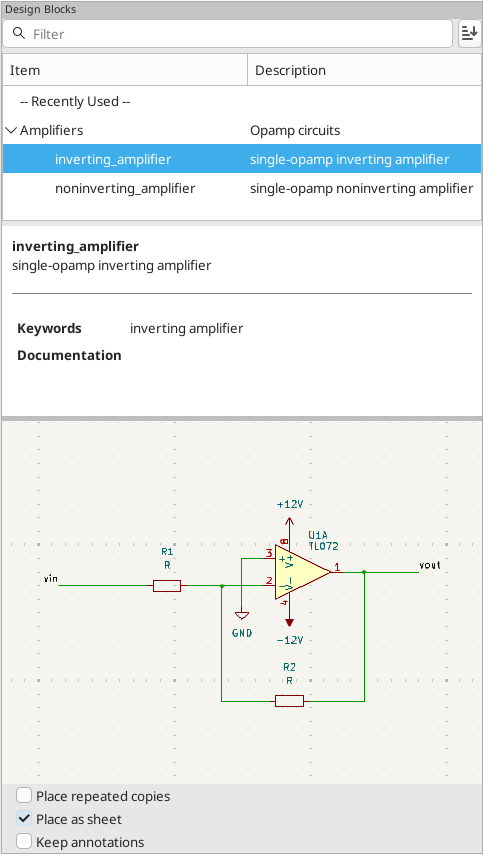
The Design Blocks panel lets you create design block libraries and create, edit, and place design blocks in the schematic.
The panel has three main areas:
-
A filter textbox at the top, for searching across all libraries by name, description, and keywords. By default results are ranked by best match. To sort alphabetically instead, select Sort Alphabetically under the
settings menu. -
A library tree that lists all registered design block libraries and the design blocks they contain. Libraries can be expanded or collapsed. A Recently Used pseudo-library at the top of the tree records design blocks you have placed recently. Right click a library and choose Pin Library to keep it at the top of the list regardless of recent usage.
-
A preview area below the tree that shows the name, description, keywords, and a graphical preview of the currently selected design block.
Creating and managing design blocks
Design blocks are saved in design block libraries, so you need to add a library before you can save any design blocks.
Creating a new design block library
To create a new library, right click in the library tree and select New Library…. This opens a file browser for you to choose a location and name for the new library. Design block libraries are saved as a folder; the folder name is the library name plus the suffix .kicad_blocks.
The file browser also lets you choose whether the new library should be added to the global design block library table or the project design block library table. Libraries in the global library table will be available to all projects, while libraries in the project library table will only be available in the current project.
| The global and project design block library tables are managed using Preferences → Manage Design Block Libraries…. This includes deleting and renaming design block libraries. The design block library tables behave in the same way as the symbol and footprint library tables. For more information about managing library tables, see the symbol library table documentation. |
After choosing a name, location, and library table, a new, empty library is created. When you create new design blocks, you can save them in this library.
Creating a new design block
In the schematic editor, design blocks can be created either from the entire contents of a schematic sheet or from a selection of schematic objects. To create and save a new design block, select the desired source objects, either by opening the desired sheet or selecting the objects in the editing canvas. Then right click the design block library that will contain the block and select Save Current Sheet as Design Block… or Save Selection as Design Block… as appropriate.
The two creation commands differ in what they capture:
-
Save Current Sheet as Design Block captures everything on the current schematic sheet. Navigate to the sheet you want to save before invoking this command. This is the most convenient option when the circuit you want to capture already exists on its own dedicated sheet.
-
Save Selection as Design Block captures only the objects that are currently selected in the canvas. Select the symbols, wires, labels, and other schematic objects you want to include before invoking this command. If the selection is a single hierarchical sheet symbol, KiCad saves the contents of that subsheet (equivalent to Save Current Sheet for that sheet). If the selection contains multiple items or a single group, those items are saved as the design block content.
After invoking either command, the Design Block Properties dialog opens.
This brings up the Design Block Properties dialog, where you can edit the properties of the new design block.
-
Name: this is the name of the new design block, which is shown in the library tree and the preview pane. It is also used when filtering design blocks with the filter textbox. When design blocks are added as a group or as a schematic sheet, this is the default name of the new group or sheet. The name may not contain the characters
/ : ; \ | < > " * ?or any character that is illegal in a library item name. -
Keywords: these are space-separated keywords describing the design block. They are displayed in the design block preview pane and used when filtering design blocks with the filter textbox.
-
Description: this is a description of the design block, which is shown in the library tree and the preview pane. It is also used when filtering design blocks with the filter textbox.
-
Default Fields: these are key/value pairs which are included as hierarchical sheet fields when the design block’s schematic is placed as a sheet. Fields are ignored when the design block is not placed as a sheet. Use default fields to pre-populate sheet-level parameters such as supply voltage, channel number, or other values that are expected to be overridden when the design block is placed as a sheet.
After filling in the properties and clicking OK, the design block is saved to the selected library. If a design block with the same name already exists in the library, KiCad will ask for confirmation before overwriting it.
When you save a selection as a design block (as opposed to saving an entire sheet), KiCad automatically groups the selected objects and sets the group’s library link to point to the newly created design block. This means the selection is ready for further design block operations immediately after saving.
You can edit a design block’s properties after creating it by right clicking the design block in the design block library tree and selecting Properties….
Deleting a design block
To delete a design block from a library, right click the design block in the library tree and select Delete Design Block. KiCad will ask for confirmation before permanently removing the design block and its directory from the filesystem. This operation cannot be undone.
Deleting a design block from the library does not affect any schematic objects that were previously placed from that design block. Existing placed groups that had a library link to the deleted design block retain their content; they simply lose the ability to use library-linked operations.
Updating an existing design block
There are multiple ways to push schematic changes back to an existing design block in the library. All of them replace the schematic content stored in the design block with new content; they do not merge changes.
Updating from a selection
This is the most general approach and works regardless of how the design block was originally placed:
-
Select the schematic objects that represent the new content for the design block.
-
In the Design Blocks panel, right click the design block you want to update and choose Update Design Block from Selection.
The stored schematic of the design block is replaced by the selection. If the design block previously had a schematic but you are updating with a new one, KiCad will ask for confirmation before overwriting.
Updating from the current sheet
If the current sheet contains exactly the content you want to store in the design block (for example, if the design block was originally placed as a hierarchical sheet and the sheet has since been edited):
-
Navigate to the sheet whose contents you want to store.
-
In the Design Blocks panel, right click the design block you want to update and choose Update Design Block from Current Sheet.
The stored schematic of the design block is replaced by everything on the current sheet.
Saving from a linked group
If the design block was placed as a group and the group has a library link:
-
Edit the schematic contents inside the group.
-
Right click the group in the canvas and choose Save to Linked Design Block.
This is the most direct workflow when iterating on a placed design block instance: edit in place, then push back to the library with a single right click.
| Updating a design block in the library does not automatically update previously placed instances of that design block. Placed instances are independent copies of the design block content at the time they were placed. To bring an existing placed instance in line with the current library version, delete it and place the updated design block again. |
Using design blocks in a schematic
You can place a design block into a schematic using the Design Blocks panel.
The Design Blocks panel contains a library tree that lists your design block libraries and the design blocks contained in each library. Each library can be expanded or collapsed to show or hide the design blocks in that library. There is a Recently Used pseudo-library at the top of the tree that contains any design blocks that you have recently placed. You can pin any libraries to the top of the list by right clicking the library and selecting Pin Library.
You can filter design blocks by their name, description, and keywords using the filter textbox at the top of the Design Blocks panel. By default, matches are sorted by best match, but you can change to sorting alphabetically by selecting Sort Alphabetically under the ![]() menu.
menu.
When you select a design block in the library tree, the design block’s name and metadata are displayed below the library tree along with a graphical preview of the design block. The metadata includes the block’s description and keywords.
To add a design block to the schematic, double click it in the library tree or right click a design block and select Place Design Block.
Placement options
There are several options controlling how the design block is placed:
-
If the Place repeated copies checkbox is enabled, KiCad will begin placing the design block again when you finish placing the previous block. To cancel placing the next block, press Esc or right click and select Cancel.
-
If the Place as group checkbox is enabled, the contents of the design block will be added to a group in the schematic, and the group’s library link will be set to point to the source design block and library. Grouping a design block keeps its contents together as a single unit in the schematic and enables library-linked operations such as saving changes back to the library, placing additional linked instances, and applying the design block layout in the PCB editor. The group can also be copied to the corresponding footprints in the board.
-
If the Place as sheet checkbox is enabled, you will need to click twice in the editing canvas to place two corners of a hierarchical sheet. The design block contents will be placed in the new sheet. If the Place as sheet checkbox is not enabled, clicking once in the canvas will place the contents of the design block directly into the current schematic. Place as group and Place as sheet can be enabled simultaneously: when both are enabled, a new hierarchical sheet is created and a group containing the sheet symbol is added to the parent schematic.
-
If the Keep annotations checkbox is enabled, KiCad will insert the design block without changing the symbol annotations as defined in the saved design block. If it is not enabled, KiCad will reset the symbol annotations while inserting the design block and reannotate all of the symbols in the block according to the current annotation settings. Keeping annotations is useful when you intend to place only a single instance of the design block in the schematic and the original reference designators are meaningful. When placing multiple instances, disable this option so that KiCad assigns unique reference designators to each instance automatically.
After placement
Once placed in a schematic, the contents of a design block behave the same as any other schematic objects and can be edited, moved, deleted, etc. exactly as if they were added to the schematic normally. If the design block was placed as a group, the group boundary is visible in the canvas. You can enter the group to edit individual items inside it, or select the entire group as a unit to move, copy, or delete all of its contents together.
Practical workflows
Workflow: creating a reusable power circuit
This workflow demonstrates saving a power supply subcircuit as a design block and reusing it in multiple projects.
-
Draw the circuit. In the schematic editor, draw the power supply circuit including symbols, wires, net labels, and power symbols. Annotate the schematic and verify it passes ERC.
-
Create or select a library. Open the Design Blocks panel (View → Panels → Design Blocks). If you do not already have a suitable library, right click in the library tree and choose New Library…. Give the library a descriptive name (for example,
power_circuits) and save it to an appropriate location. Add it to the global library table so it is available in all projects. -
Select the circuit. In the canvas, draw a selection box around all the symbols, wires, and labels that make up the power supply circuit.
-
Save as design block. Right click the target library in the Design Blocks panel and choose Save Selection as Design Block…. In the Design Block Properties dialog, enter a meaningful name, a brief description, and relevant keywords (for example,
LDO 3.3V linear regulator). Click OK. KiCad saves the design block and automatically groups the selected objects with a library link to the new design block. -
Reuse in another project. Open a different project. Open the Design Blocks panel and expand the
power_circuitslibrary. Find the design block you created (use the filter if needed). Enable Place as group and, if the reference designators should be reassigned, disable Keep annotations. Double click the design block to begin placement and click in the canvas to place it. -
Update the design block later. If you improve the power supply circuit, select the placed group, edit it as needed, then right click the group and choose Save to Linked Design Block to push the changes back to the library.
Workflow: sheet-based reuse with hierarchical parameters
This workflow is suited for a design block that represents a complete functional block with parameters that vary between instances, such as a per-channel analog conditioning circuit.
-
Draw the circuit on a dedicated sheet. Create a hierarchical sheet in your project and draw the channel circuit on it, using hierarchical labels for signals that connect to the parent sheet. If the circuit has configurable values (such as a gain-setting resistor value), note which sheet fields you will use to communicate these.
-
Define default fields. Open the Design Blocks panel and save the sheet as a design block using Save Current Sheet as Design Block…. In the Design Block Properties dialog, add default fields for each hierarchical parameter. For example, add a field named
GAIN_Rwith a default value of10k. -
Place as a sheet. In the parent schematic, open the Design Blocks panel, select the design block, enable Place as sheet, and click twice in the canvas to define the sheet symbol boundary. KiCad creates a new hierarchical sheet symbol and populates it with the default fields from the design block.
-
Customize each instance. For each placed hierarchical sheet, open the sheet properties and adjust the field values to match the requirements for that particular instance (for example, different resistor values for different gain settings). The sheet contents are shared (all instances use the same underlying schematic file from the design block), but the field values are per-instance.
-
Updating. If the underlying circuit changes, save the modified sheet as an update to the design block using Update Design Block from Current Sheet. All instances of the hierarchical sheet in the project will automatically reflect the updated schematic, because they all reference the same subsheet file.
仿真器
KiCad provides an embedded electrical circuit simulator using ngspice as the simulation engine. ngspice is a SPICE simulator derived from the original widely used Berkeley SPICE program. KiCad’s simulator can also run simulations using IBIS models of device pins.
The process of creating and running a simulation in KiCad has two main parts:
-
Drawing a simulation schematic in KiCad’s Schematic Editor. Schematics for simulations are similar to normal schematics (and can even be identical), but they typically include simulation-specific devices, such as sources, and may exclude devices that are irrelevant for simulation, such as connectors. Creating a schematic simulation requires ensuring all symbols in the schematic have appropriate models assigned. Finding or creating simulation models, and then validating them, can be a significant portion of the process. KiCad includes some simple simulation models for basic devices such as sources, passive devices, and generic semiconductor devices, but beyond those you will need to find or create your own models.
-
Running the simulation using the simulator tool. This includes choosing the type of analysis (transient, AC, etc.) and configuring its options. Multiple different analyses can be performed. The simulator provides a plot window to view and analyze simulation results.
When drawing schematics for simulation, the Simulation_SPICE symbol library, installed with KiCad by default, may be useful. It contains common elements used for simulation such as voltage and current sources, generic semiconductor symbols, and other simulation-specific devices. The symbols in this library are described in detail below.
While these elements enable a great variety of simulation work, users familiar with SPICE in other environments will be used to incorporating models of commercially-available semiconductors, integrated circuits, and other devices as more complex SPICE models. Indeed, semiconductor manufacturers often freely supply these to help users simulate and develop circuits using their parts. Note that while KiCad does not include any commercial SPICE models in its distribution, you are free to use any models you may have, or have used with other circuit simulators, in KiCad’s simulator.
In general, if a model works with other SPICE simulators, it should work with the KiCad simulator, although some SPICE simulators implement extensions that are unsupported by ngspice. ngspice offers several compatibility modes to improve compatibility with other simulators.
Finally, to quickly showcase the capabilities of the KiCad simulator, some demonstration projects are included in the KiCad distribution. They can be found in the demos/simulation directory.
分配模型
您需要先将仿真模型分配给符号,然后才能仿真您的电路。
每个符号只能分配一个模型, 即使该符号包含多个单元也是如此。 对于具有多个单元的符号, 您应该将模型分配给第一个单元。
SPICE 模型信息以文本形式存储在符号字段中。 因此,您可以在符号编辑器或原理图编辑器中定义它。 要将仿真模型分配给符号,请打开符号属性对话框并单击 仿真模型… 按钮,这将打开仿真模型编辑器对话框。
You can exclude a symbol from simulation entirely by checking the exclude from simulation checkbox in the Symbol Properties dialog. Symbols with this attribute set are drawn with a grey outline and a small simulation icon next to them, as shown below.
推断模型
电阻、电感和电容的模型是可以推断,这意味着 KiCad 将检测到它们是无源的并自动分配适当的仿真模型。 因此它们不需要任何特殊设置; 用户只需要设置符号的 值 字段即可。
KiCad 根据以下标准推断符号的仿真模型:
-
该符号恰好有两个引脚,
-
位号以
R,L或C开头。
Inferred models are ideal models. If the simulation requires a non-ideal model, for example an inductor with parasitic capacitance included, you must explicitly assign a model that includes it.
内置模型
KiCad offers several standard simulation models. They do not require an external model file, and their parameters can be edited in KiCad’s Simulation Model Editor GUI. The following devices are available:
-
Resistors (including potentiometers)
-
Capacitors
-
Inductors
-
传输线
-
开关
-
电压源和电流源
-
二极管
-
Transistors (BJTs, MOSFETs, MESFETs, and JFETs)
-
XSPICE code models
-
原始SPICE元素
To add a built-in model to a symbol, open the Simulation Model Editor dialog (Symbol Properties → Simulation Model…) and select Built-in SPICE model. You can then select the kind of device from the device dropdown and the device subtype from the device type dropdown.
Refer to the ngspice documentation for more details about these models and their parameters.
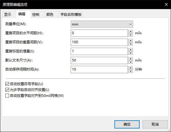
Device sets the type of device to simulate: a resistor, BJT, voltage source,
etc. This value is stored in the symbol’s Sim.Device field.
Device type selects the type of model to use for the device. Most devices
have several types of models to choose from. Models may vary in their degree of
accuracy, which characteristics they are optimized for, what parameters they
have available, and how many pins they have. For example, the ideal
resistor type models a simple resistor with two terminals and a single
resistance parameter, while the potentiometer resistor type models an
adjustable resistor with three terminals and an additional parameter for wiper
position. Some devices have an especially large number of types to choose from:
N-channel MOSFETs, for example, have 17 available types, each of which uses a
different mathematical model to simulate the transistor behavior. One model may
be more or less appropriate than another for simulating a specific device or
circuit or for performing a particular analysis. Refer to the
ngspice documentation for detailed
information about models and their parameters. The device type value is
stored in the symbol’s Sim.Type field.
参数 选项卡显示元件的参数并允许您编辑它们。 例如,电阻器的电阻、电压源的波形、MOSFET 的宽度和长度等。任何与模型默认值不同的参数都存储在符号的 Sim.Params 字段中。
编码 选项卡显示生成的 SPICE 模型,因为它将被写入 SPICE 网表以进行仿真。
在值字段中的保存参数 '<parameter name>' 复选框使用符号的 值 字段而不是 Sim.Params 字段来存储参数。 这可以更轻松地从原理图编辑简单模型,而无需打开仿真模型编辑器。 此选项仅适用于理想的无源模型(R、L、C)和直流电源。 如果符号中存在 Sim.Params 字段,它将优先于 值 字段。
External models
KiCad can also load SPICE models from external files. This is typically how you will add a SPICE model of a specific commercially-available part (for example, a 555 timer or a TL071 operational amplifier) to your simulation. Models such as these are readily available from numerous sources, including manufacturers' web sites. These models must be in a standard SPICE format and must not be encrypted.
An external model can be one of the following types:
-
A device model (
.model). This is an intrinsic device (a passive, diode, transistor, etc.) with a set of parameter values defining its behavior. The parameters for a device model are editable in the Simulation Model Editor GUI. -
A subcircuit model (
.subckt). This is a model that uses a collection of other ngspice circuit elements to define its behavior. If a subcircuit model contains parameters (in aparams:sequence in its definition), the parameters are editable in the Simulation Model Editor GUI.
要从外部文件加载模型,请打开仿真模型编辑器对话框(符号属性 → 仿真模型…)并从文件中选择 SPICE 模型。
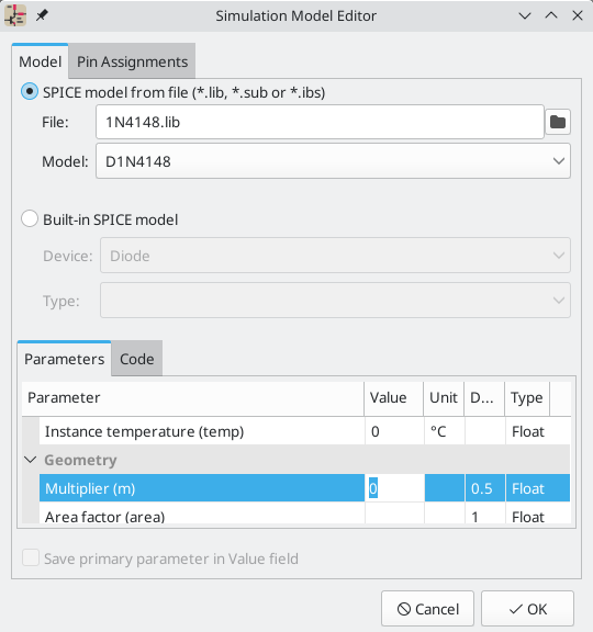
File is the path to the model file to use. Unencrypted model files are plain, human-readable text files and often have extensions such as .lib, .sub etc., although KiCad will accept a valid model with any extension.
The path to the file can be absolute, or relative to the project folder. The path can also be relative to the value of SPICE_LIB_DIR if you have defined that path variable. If you enable the Embed File checkbox in the file browser, the library file will be embedded in the schematic (or symbol library). This makes the schematic (or schematic) more portable as it doesn’t rely on an external library file. The library filename is saved in the symbol’s Sim.Library field.
Model is the name of the desired model in the model file. A model file may contain multiple models, and if so they will all be shown in the list. You can filter the list of models using the search box. The selected model is listed in the symbol’s Sim.Name field.
Parameters can be overridden (or additional parameters specified) using the Parameters tab. For device models, all parameters for that type of device are editable. For subcircuit models, any parameters included in the subcircuit definition are editable. Any parameters that are overridden in the Parameters tab are stored in the symbol’s Sim.Params field.
The Code tab displays the generated SPICE model as it will be written to the SPICE netlist for simulation.
| KiCad is not distributed with SPICE models for specific commercial devices. These models are usually available from device manufacturers or other internet sources. |
IBIS models
IBIS(I/O 缓冲区信息规范)文件是 SPICE 模型的替代品,用于对数字部件上的输入/输出缓冲区的行为进行建模。 为了加载 IBIS 文件,用户应遵循 SPICE 库模型的相关流程,并提供一个 .ibs 文件。
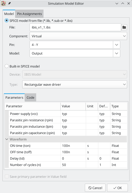
File is the path to the model file to use. The path can be absolute or
relative to the project folder. The path can also be relative to the value of
SPICE_LIB_DIR if you have
defined that path variable.
The library filename is saved in the symbol’s Sim.Library field. If an IBIS
model file is loaded, the remaining fields in the dialog will relate to the IBIS
model.
Component selects which component from the IBIS file to use, as IBIS files
can contain multiple components. The component name is saved in the symbol’s
Sim.Name field.
Pin selects which pin in the IBIS model to simulate. The selected pin must
be mapped to a symbol pin in the Pin Assignments tab. The chosen pin’s
number is saved in the symbol’s Sim.Ibis.Pin field.
Model is the list of models available for the selected pin, for example an
input or an output. The chosen model name is saved in the symbol’s
Sim.Ibis.Model field.
Type selects what the pin should do in the simulation. A pin can be a passive
device that doesn’t drive any value; it can be a DC driver that drives
high, low, or high-impedance; or it can be a rectangular wave or
PRBS driver. This value is stored in the symbol’s Sim.Type field.
参数 选项卡可让您查看和编辑模型的参数。 对于每个参数,您可以在 IBIS 文件中定义的最小值、典型值或最大值之间切换。 您还可以根据引脚选择的类型来选择驱动波形的参数。 任何不同于默认值的参数都存储在符号的 Sim.Params 字段中。
| KiCad 不附带符号的 IBIS 模型。 IBIS 模型通常可从设备制造商处获得。 |
KiCad 的 Simulation_SPICE 符号库提供了几个可能对 IBIS 仿真有用的符号。 IBIS_DEVICE 可用于元件(输入)引脚,而 IBIS_DRIVER 可用于仿真驱动器引脚。 每个差分引脚也有类似符号。
|
引脚分配
Simulation models may have their pins numbered differently than the corresponding symbol. For example, SPICE models for diodes usually consider pin 1 to be the anode, while schematic symbols are usually drawn with pin 1 as the cathode. Operational amplifier models are also very likely to have model pin assignments that do not match package or schematic pin numbers.
您可以使用仿真模型编辑器的 引脚分配 选项卡将符号的引脚映射到仿真模型引脚。
| Always make sure symbol pins are correctly mapped to simulation model pins. Mistakes here can lead to erroneous or confusing simulation results, or a failure to simulate at all. |
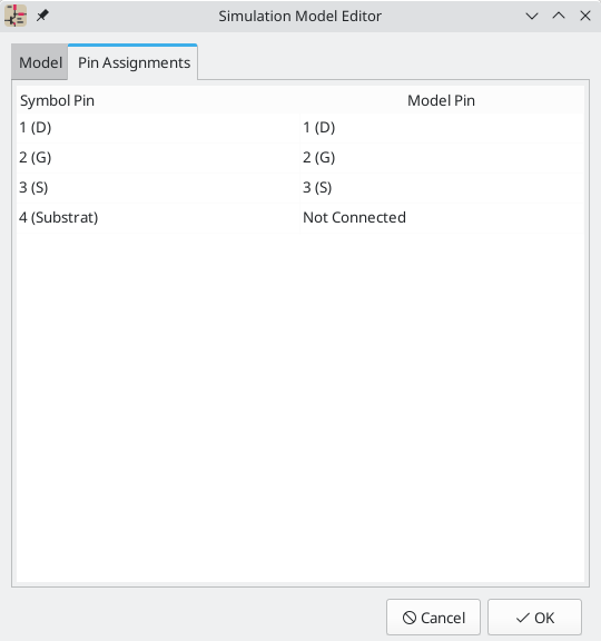
The left column displays the name and number of each symbol pin, i.e. the pin numbers and names that appear on the schematic part in KiCad. The right column displays the corresponding pin as defined in the model file in use. For each symbol pin, you can select the corresponding pin from the simulation model in the dropdown in the right column. In the cases where a schematic part has pins that are not in the model, as in the case of an operational amplifier with 'nulling' pins that are not modeled, the schematic part pin may be assigned to the 'Not Connected' option in the Pin Assignments dropdown. Unlike other pin assignments, 'Not Connected' may be assigned to multiple pins if necessary.
When you use a subcircuit model, the dialog displays the model’s code under the pin assignments for use as a reference while assigning pins. A well-written model will often include a helpful reference section (as a set of comments) to inform the user how the model pins are mapped.
值的表示
The simulator supports several notations for writing numerical values in simulation model parameters, simulation analysis setup options, and SPICE directives:
-
简单表示法 :
10100,0.003, -
科学表示法:
1.01e4,3e-3, -
前缀表示法:
10.1k,3m. -
RKM 表示法:
4k7,10R.
You can mix prefix and scientific notations. As such, 3e-4k is a valid input and is equivalent to 0.3. The list of valid prefixes is shown below. They are case sensitive.
| Prefix | Name | Multiplier |
|---|---|---|
a |
atto |
10-18 |
f |
femto |
10-15 |
p |
pico |
10-12 |
n |
nano |
10-9 |
u |
micro |
10-6 |
m |
milli |
10-3 |
k |
kilo |
103 |
M |
mega |
106 |
G |
giga |
109 |
T |
tera |
1012 |
P |
peta |
1015 |
E |
exa |
1015 |
Raw SPICE Element models and directives are passed to ngspice directly, without KiCad reformatting the values for ngspice to consume. ngspice uses a different, case-insensitive notation: 1 mega (106) is denoted there as 1Meg, while 1M is 1 milli (10-3). Depending on the compatibility mode selected, ngspice may not support the same value notations as KiCad, so care should be taken when using raw SPICE elements and simulation directives.
|
SPICE 标识符
可以在原理图图纸的文本字段中放置 SPICE 标识符。 这种方法便于定义默认模拟类型。 文本字段中支持的标识符列表是:
-
以点开头的标识符(例如
.tran 10n 1m) -
电感耦合系数(例如
K1 L1 L2 0.89)
无法使用文本字段放置其他元件。
If a simulation command is included in schematic text, the simulator will use it as the simulation command when you open the simulator. However, you can override it by choosing a different simulation type in the Simulation Command dialog. You can also specify simulation commands with raw SPICE commands by using the Custom analysis type.
有关 SPICE 标识符的更多详细信息,请参阅 ngspice 文档。
运行仿真
Circuits for simulation are drawn in the Schematic Editor, but simulations are run in the Simulator window.
After creating a schematic for simulation, the following steps are needed to run a simulation:
-
Open the simulator window by clicking Inspect → Simulator in the Schematic Editor or using the
 button in the top toolbar.
 -
Create at least one analysis by clicking Simulation → New Analysis Tab… (Ctrl+N) or using the
 button. This lets you choose a type of simulation and configure its options. These options are explained below. Each analysis has its own tab, and multiple analyses can be created. The options for an analysis can be adjusted after it is created with Simulation → Edit Analysis Tab… or by clicking on the
  button.
 -
Run the simulation by clicking Simulation → Run Simulation (R) or by clicking the
 button. This only runs the simulation in the active analysis tab. You can stop a running simulation at its current point by clicking the
  button.
 -
Examine the simulation results. Most analyses result in plots; for these you will need to select the signals to be plotted. Other analyses print their results in the output log window.
| Once a simulation has been set up, the configuration can be saved in a workbook. |
Simulator window
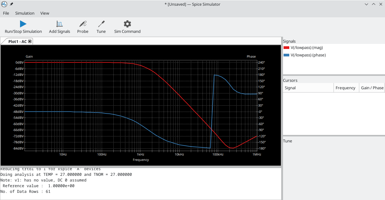
The simulator window is divided into several sections:
-
窗口顶部有一个工具栏,其中包含常用操作的按钮。
-
The main part of the window graphically shows the simulation results. The simulation needs to run and signals need to be selected from the list of available signals or probed before they are displayed in the plot.
-
Below the plot panel, the output log window shows logs from the ngspice simulation engine. Some types of analyses print their results here.
-
The right side of the window displays a list of signals, a list of active cursors, measurements, and a tuning tool for adjusting component values based on simulation results.
Simulation types
Each simulation is a specific type of analysis. The following analysis types are available:
Each analysis type and its options are explained below. You can configure an analysis when you create it (![]() button) or by editing an existing analysis (
button) or by editing an existing analysis (![]() button). These analysis types are explained in more detail in the ngspice documentation.
button). These analysis types are explained in more detail in the ngspice documentation.
| Another way to configure a simulation is to type SPICE directives into text fields on schematics. Any text field directives related to a simulation command are overridden by the settings selected in the dialog. This means that once a simulation has run, the dialog overrides the schematic directives until the simulator is reopened. |
Operating point analysis (OP)

Calculates the DC operating point of the circuit. This analysis has no options.
Operating point analyses do not have any plotted results. Results are printed in the output log window. You can also display the node voltages and device currents calculated by this analysis as annotations in the schematic.
DC sweep analysis (DC)
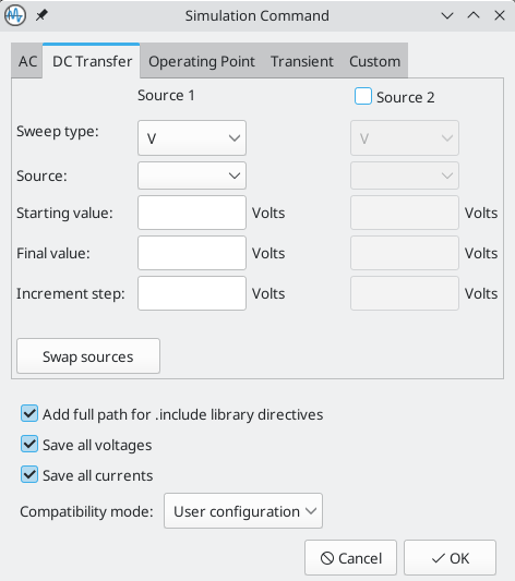
Calculates the DC behavior of the circuit while sweeping one or two parameters. The following parameters can be swept:
-
value of an independent voltage source
-
value of an independent current source
-
value of a resistor
-
simulation temperature
DC analyses have the following options, which are listed here with the corresponding ngspice parameter name:
-
Sweep type: the type of variable to sweep. This can be a voltage source, a current source, a resistor, or the simulation temperature.
-
Source: the particular voltage source, current source, or resistor to sweep (
srcnam). The list is populated with each item in the schematic of the relevant type. It is disabled for temperature sweeps. -
Starting value: the starting value for the sweep (
vstart). -
Final value: the ending value for the sweep (
vstop). -
Increment step: the amount to increase the value at each step of the sweep (
vincr). Smaller increments result in more output points.
If Source 2 is enabled, the same options are available to simultaneously sweep a second source. When sweeping two sources, Source 1 is swept over its entire range for each value of Source 2. In other words, each value for Source 2 results in a separate curve, and each curve shows a full sweep of Source 1 with Source 2 held constant at a particular value.
Clicking the Swap sources buttons swaps Source 1 with Source 2.
输出显示为绘图。
| The tuning tool is another way to see how component values affect circuit behavior. Unlike DC sweeps, the tuning tool can be used with other types of simulations, like transient or AC analyses. |
AC small-signal analysis (AC)
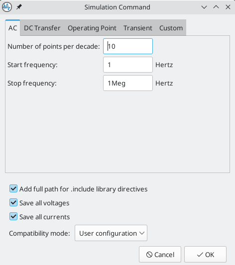
Calculates the small-signal AC behavior of the circuit in response to a stimulus. Performs a decade sweep of stimulus frequency.
To run an AC analysis you must choose a number of points to measure per decade and the start and end frequencies for the decade sweep.
AC analyses have the following options, which are listed here with the corresponding ngspice parameter name:
-
Number of points per decade: the number of points to calculate per decade (
nd). -
Start frequency: the lower bound of the frequency range to analyze (
fstart). -
Stop frequency: the upper bound of the frequency range to analyze (
fstop).
The output is displayed as a Bode plot (output magnitude and phase vs. frequency).
Transient analysis (TRAN)
计算电路的时变行为。
Transient analyses have the following options, which are listed here with the corresponding ngspice parameter name:
-
Time step: a suggested time step (
tstep). -
Final time: the time at which the simulation will end (
tstop). -
Initial time: the time at which the simulation will start (
tstart). If not specified, this defaults to 0. -
Max time step: the maximum time step (
tmax). If not specified, this defaults to the suggested time step or the total simulation duration divided by 50, whichever is smaller. -
Use initial conditions: if enabled, the simulator will not calculate the quiescent operating point before starting the transient simulation. Instead, the simulation will use the initial conditions specified in a
.icdirective and elementICparameters. This corresponds to ngspice’suicoption.
输出显示为绘图。
Pole-zero analysis (PZ)
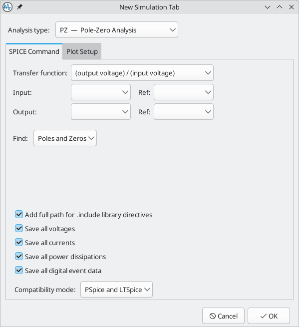
Calculates the poles and zeroes of the small-signal (AC) transfer function of the circuit.
Pole-zero analyses have the following options, which are listed here with the corresponding ngspice parameter name:
-
Transfer function: selects between calculating the transfer function as output voltage divided by input voltage or output voltage divided by input current. These correspond to ngspice’s
volandcuroptions, respectively. -
Input: the input node (
node1) and the reference node for the input (node2). -
Output: the output node (
node3) and the reference node for the output (node4). -
Find: selects between calculating poles and zeroes, only poles, or only zeroes. These correspond to ngspice’s
pz,pol, andzeroptions, respectively.
Operating point analyses do not have any plotted results. Results are printed in the output log window.
Noise analysis (NOISE)
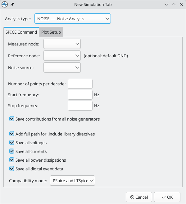
Calculates the noise generated by the devices in the circuit, both as output noise and input-referred noise. The noise spectrum (V/√Hz or A/√Hz) of the circuit can be plotted, and the total noise over the specified frequency range is reported. Optionally, the noise contributions of each device are reported individually.
Noise analyses have the following options, which are listed here with the corresponding ngspice parameter name:
-
Measured node: the node at which output noise is measured (
output). -
Reference node: the reference node for measuring the output noise (
ref). The output noise is calculated as the noise at the measured node minus the noise at the reference node. If it is not specified, the default is the ground node. -
Noise source: a source that is considered the circuit’s input for the purposes of calculating input-referred noise (
src). The source must specify an AC magnitude, i.e. the source must have anacparameter. -
Number of points per decade: the number of points to calculate per decade (
pts). -
Start frequency: the lower bound of the frequency range to analyze (
fstart). -
Stop frequency: the upper bound of the frequency range to analyze (
fstop). -
Save contributions from all noise generators: if enabled, noise magnitudes of individual noise generators are saved and reported. If disabled, only the overall output and input-referred noise over the specified frequency range are reported.
The output and input-referred noise spectra can be plotted. Total noise values for the specified frequency range are printed in the output log window.
S-parameter analysis (SP)
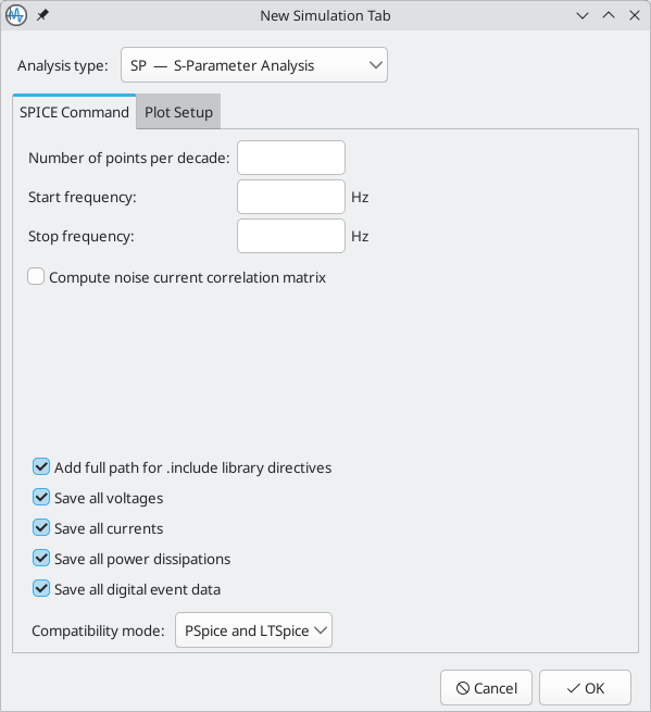
Calculates the scattering parameters, admittance matrix, and impedance matrix for the circuit. Optionally calculates the noise current correlation matrix. Note that this analysis requires at least two voltage sources configured as RF ports as described in the ngspice manual.
S-parameter analyses have the following options, which are listed here with the corresponding ngspice parameter name:
-
Number of points per decade: the number of points to calculate per decade (
nd). -
Start frequency: the lower bound of the frequency range to analyze (
fstart). -
Stop frequency: the upper bound of the frequency range to analyze (
fstop). -
Compute noise current correlation matrix: if enabled, the noise current correlation matrix is also calculated. This corresponds to ngspice’s
donoiseoption.
输出显示为绘图。
Frequency content analysis (FFT)
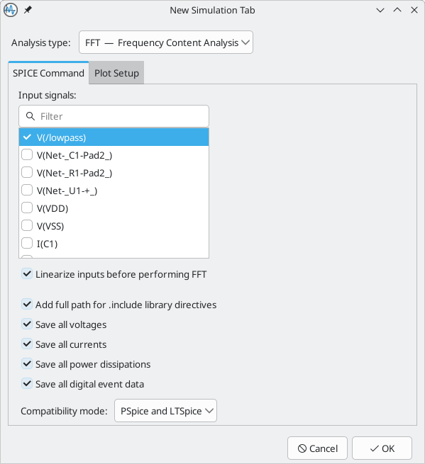
Calculates an FFT based on an existing analysis tab. Any of the signals from an existing analysis can be used as inputs to the FFT. The signals are windowed using a Hanning window.
FFT analyses have the following options, which are listed here with the corresponding ngspice parameter name:
-
Input signals: the signal(s) to perform an FFT on. An FFT is independently applied to each selected signal.
-
Linearize inputs before performing FFT: When enabled, the input vector is converted to have equidistant time points prior to performing the FFT. Corresponds to ngspice’s
linearizecommand.
输出显示为绘图。
Custom analysis
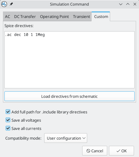
Performs a SPICE analysis defined by raw SPICE analysis commands (.tran, .ac, .dc, .noise, etc.). For details on such analysis commands and their syntax, refer to the ngspice documentation.
The analysis commands given on each line of the SPICE directives textbox are run as separate analyses. If you click the Load Directives from Schematic button, any SPICE directives in schematic text are copied into the textbox.
额外的仿真设置
There are several simulation options that apply to all types of simulations. These are located at the bottom of the dialog.
-
Add full path for .include library directives: if enabled, relative paths to SPICE models will be converted to absolute paths in the SPICE netlist.
-
Save all voltages: if enabled, the simulator will save voltages for each node in the simulation results so that they can be plotted. This corresponds to ngspice’s
.save allcommand in the SPICE netlist. If disabled, voltages will not be saved in the results, and therefore cannot be plotted, unless a SPICE directive is used to manually probe a node voltage. -
Save all currents: if enabled, the simulator will save currents through each device pin in the simulation results so that they can be plotted. This corresponds to ngspice’s
.probe allicommand in the SPICE netlist. If disabled, currents will not be saved in the results, and therefore cannot be plotted, unless a SPICE directive is used to manually probe a current. -
Save all power dissipations: if enabled, the simulator will save power dissipations for each device in the simulation results so that they can be plotted. This corresponds to ngspice’s
.probe P(<device>)command in the SPICE netlist for each device in the schematic. If disabled, power dissipations will not be saved in the results, and therefore cannot be plotted, unless a SPICE directive is used to manually probe a power dissipation. -
Save all digital event data: if enabled, the simulator will save digital event data for digital (event-driven) simulation models. This corresponds to ngspice’s
.esave allcommand. If disabled, digital event data will be discarded. -
兼容模式下拉列表选择仿真器用于加载模型的兼容模式。 用户配置 选项是指用户的
.spiceinitngspice 配置文件。 兼容模式在 ngspice 文档 中进行了描述。
Viewing simulation results
Each analysis has its own tab, containing its own separate plot, signal list, and output log window. Only the active tab is updated when a simulation is run. In this way it is possible to compare simulation results between different runs.
Simulation results from most analysis types are visualized as plots. However, DC Operating Point (OP) and Pole-zero (PZ) analyses do not generate plots. Instead, they print their results in the output log at the bottom of the simulator window. OP analysis results can additionally be displayed as annotations on the schematic canvas.
Plotted results
Most types of analyses display their results in a plot. The type of plot depends on the analysis: transient simulations display signal values over time, for example, while AC simulations display results in a Bode plot.
You can zoom and move a plot using the following gestures:
-
Scroll mouse wheel to zoom in/out. Shift, Ctrl, and Alt can modify the scroll action depending on the configuration in the Simulator panel in the Schematic Editor Preferences.
-
Right click to open a context menu to adjust the view.
-
Draw a selection rectangle to zoom in the selected area.
-
Drag a cursor marker to move the cursor.
The list of signals that can be plotted in the active plot is shown in the Signals pane on the right side of the simulator window. The following types of signals can be plotted:
-
Node voltages: the voltage of each net in the schematic, displayed as
V(<net>). -
Device node currents: the current for each device in the schematic, displayed as
I(<device>)orI(<device:terminal>). For two-terminal devices, the device’s current is listed as a single signal corresponding to the current into the device’s pin 1. For devices with more than two terminals, the current into each terminal is a separate signal. -
Device power dissipations: the power dissipated by each component, displayed as
P(<device>). -
User-defined signals: custom signals defined as an expression based on other signals. User-defined signals can be arbitrary mathematical expressions. One common use for user-defined signals is to plot a voltage differential, i.e. the voltage between two points.
To plot a signal, check the box in the plot column next to the signal of interest. To remove a signal from the plot, clear its checkbox.
You can also interactively select signals to plot by using the Probe Schematic tool. To activate the tool, use Simulation → Probe Schematic… (P) or click the (![]() ) button. When activated, the tool lets you click elements in the schematic to plot the corresponding signal. Different types of signals are probed depending on what you click:
) button. When activated, the tool lets you click elements in the schematic to plot the corresponding signal. Different types of signals are probed depending on what you click:
-
Clicking on a wire plots the voltage of that net. When you hover over a wire, the net is highlighted to indicate that its voltage can be probed.
-
Clicking on a symbol pin plots the current going into that pin. When you hover over a pin, the cursor changes to a current clamp to indicate that clicking will probe the current.
KiCad does not support ngspice’s .plot directive. This directive has no
effect when a simulation is run using KiCad.
|
Plot settings and appearance
Colors of individual signals may be set by clicking the color field associated with each signal in the Signals grid. You may choose from a predefined palette (Defined Colors), or select a custom color (Color Picker). You can toggle the color of the plot background from black to white with View → Dark Mode Plots (this affects all analysis tabs, not just the active tab).
Many plot settings can be configured in the Plot Setup tab of the Analysis Setup window (![]() button).
button).
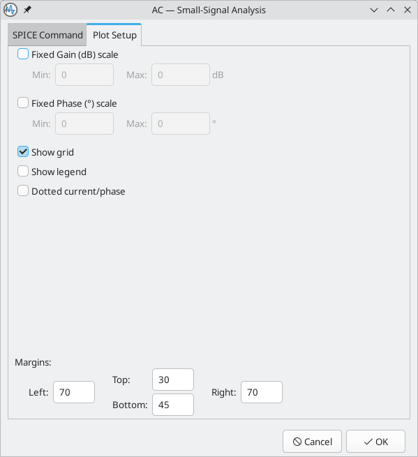
-
Fixed scale: when enabled, this fixes the vertical and/or horizontal plot scales to the specified ranges. Manually zooming will not affect an axis if its scale is fixed.
-
Show grid: when enabled, a grid will be shown behind the plotted signals. You can also turn the grid on or off with View → Show Grid.
-
Show legend: when enabled, a legend will be shown on the plot for the enabled signals. You can reposition the legend by dragging it.
-
Dotted current/phase: when enabled, plotted signals representing current (transient simulations) or phase (AC simulations) are displayed using dotted lines instead of solid lines. You can also enable this setting with View → Dotted Current/Phase.
-
Margins: this controls the padding on each side of the plot.
Cursors
For precise measurement, cursors are available in the plot window. You can add a cursor to a signal by checking the Cursor 1 or Cursor 2 checkbox for the signal in the signal grid on the right. Each cursor always tracks its signal: the intersection of the cursor’s horizontal and vertical lines is always exactly on the signal.
Once cursors have been added, the horizontal position of each cursor is shown by a number in a triangular marker at the top of the plot display. You can reposition each cursor by clicking and dragging its marker. The vertical position of each cursor tracks its assigned signal. The horizontal and vertical value for each cursor are shown in the cursor grid on the right of the simulator window. If cursors 1 and 2 are both enabled, the difference between them is also shown.
When you are tuning in Multi Run mode, and multiple curves are plotted for each signal, you can move a cursor from one plotted curve to another curve of the same signal by dragging it with the mouse. The cursor will follow the plotted curve that is closest to the mouse position.
To precisely position a cursor, you can directly edit its horizontal position in the cursors grid. You can also modify the display format (unit range and number of significant digits) by right clicking a value in the cursors grid and clicking Format for the relevant quantity.
You can also add more cursors beyond the two default cursors. To create more cursors, right click on a signal in the signals grid and click Create new cursor. To remove an extra cursor, right click in a one of the extra cursor columns and click Delete cursor 3 (or whichever cursor you want to delete).
Measurements
You can add automatically calculated measurements for any plotted signal, such as a minimum, average, or peak-to-peak measurement.
| Measurements are made over all the data resulting from the simulation, not just the data that is visible in the plot window at the current zoom setting. |
| It is not necessary to have selected a signal for plotting (by selecting its Plot checkbox) in order to make a measurement on it. Even unplotted signals can be measured. |
To add a predefined measurement to a signal, right click on a signal in the signals grid and select a measurement. The following measurements are available:
-
Measure Min: measures the minimum value of the entire signal
-
Measure Max: measures the minimum value of the entire signal
-
Measure RMS: measures the root-mean-square value of the entire signal
-
Measure Peak-to-peak: measures the peak-to-peak value of the entire signal
-
Measure Time of Min: measures the time at which the minimum value of the entire signal occurs
-
Measure Time of Max: measures the time at which the maximum value of the entire signal occurs
-
Measure Integral: computes the time integral value of the entire signal
-
Perform Fourier Analysis: performs a Fourier analysis of the selected signal based on a specified fundamental frequency. Calculates the amplitude of the harmonics of the fundamental as well as the total harmonic distortion. This measurement is only available for transient analyses, and its results are printed in the simulation log window instead of in the measurement panel.
Measurement results are displayed in the Measurement pane at the lower right of the simulator window. Multiple measurements will display as multiple rows in this area. You can delete a measurement by right clicking it and clicking Delete Measurement. To modify the display format of a measurement result (unit range and number of significant digits), right click the value and click Format Value….
The above context menu options are a shortcut for directly specifying measurements in the the Measurement pane. To manually create a new measurement, click in an empty row in the Measurement pane and type in an ngspice measurement function. You can also edit existing measurements by clicking on them. For more information about measurements and their syntax, refer to the ngspice manual.
Numerical results
While most analyses display their results as plots, DC Operating Point (OP) and Pole-zero (PZ) analyses do not result in plots. Instead, these analyses print their results as text in the simulation log window.

Operating point annotations
For the OP analysis, annotations can also be added to the schematic indicating the operating point voltage and current values at the nodes. Operating point voltage annotations can be shown or hidden for every node with View → Show OP Voltages. Operating point current annotations can be shown or hidden for every symbol pin with View → Show OP Currents. These annotations are globally shown or hidden for every node or every pin. You can control the formatting of these annotations in the Formatting panel of Schematic Setup.

You can also display operating point results using text variables. Using text variables requires more work to set up but provides more control over how the data is displayed. For example, you can use text variables to display only certain voltages or currents, or to control the display formatting of particular values. You can also use text variables to display power dissipation measurements.
To use text variables to display an operating point voltage for a net, add a label to the net, then add a field to that label. The label can contain any text as long as it contains the ${OP} text variable. The text variable can contain formatting specifiers in the form ${OP.<precision><unit>}, but both the precision and unit are optional. Precision is the number of significant digits to display, which is 3 by default. Unit is the unit to use, including a prefix, such as mV for millivolts.
As an example, a label field containing the text Vout: ${OP}, attached to a net with an operating point voltage of 5.123V, displays as "Vout: 5.12V". The text ${OP.4mV} displays as "5123mV", ${OP.2} displays as "5.1V", and ${OP.mV} displays as "512mV".
Using text variables to display an operating point current into a device pin is similar, but uses symbol fields instead of label fields. The field can contain any text as long as it contains the ${OP:<pin>} text variable. The pin can be specified as a pin name or a pin number. For two-terminal devices, the pin can be omitted, and the current into the device’s pin 1 will be reported. The same optional formatting specifiers are supported as for voltages, in the form ${OP:<pin>.<precision><unit>}.
For example, in a symbol with an operating point current of 5.123mA through pin 1 (pin name C), a symbol field containing the text Ic: ${OP:C} displays as "Ic: 5.12mA". The text ${OP:C.2mA} displays as "5.1mA", ${OP:1.4} displays as "5.123mA", and ${OP:C.A} displays as "0.00512A".
You can also use text variables to display a device’s power dissipation. This works identically to current, but with power instead of a pin name or number. For example, in a symbol with an operating point power dissipation of 5.123mW, a symbol field containing ${OP:power.2mW} displays as "5.1mW".
| Don’t forget to set the label field or symbol field to visible, or it will not be displayed. |
User-defined signals
In addition to the list of signals that come from the nets in the schematic, you can define your own signals which behave like normal signals in most respects. User defined signals are defined as mathematical operations on one or more basic signals.
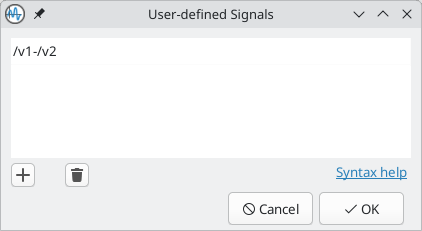
To add a user-defined signal, open the User-defined Signal dialog with Simulation → User-defined Signals… (![]() button) and add a signal. The new signal will appear in the Signal grid, where it can be plotted and used like any other signal. User-defined signals are also included in OP results.
button) and add a signal. The new signal will appear in the Signal grid, where it can be plotted and used like any other signal. User-defined signals are also included in OP results.
| Unlike normal signals, which are plotted incrementally as a simulation progresses, user-defined signals are not plotted until the simulation completes. |
One use for user-defined signals is to plot a differential voltage, i.e. the voltage between two arbitrary nodes. For example, to plot the voltage difference between the nets /v1 and /v2, you can create a user-defined signal with the expression /v1-/v2 and then plot it. This expression could also be written in a number of different ways, for example V(/v1)-V(/v2) or V(/v1,/v2), which are both equivalent.
A number of mathematical functions are available for use in user-defined signals. To see a list, click the Syntax help link in the User-defined Signals dialog. Refer to the ngspice manual for details on each of these functions.
Net names may contain special characters that have particular meaning to
the ngspice interpreter. In particular, ngspice interprets the dash
character (-) as a subtraction operation. To ensure that net names are
interpreted correctly, surround the net name with double quote (")
characters when referring to it in a user-defined signal.
|
调整元件
The simulator has a tuning tool, which lets you observe how changing a component value affects the simulation results. Each time the component value is tuned, the simulation is re-run with the new component value. You can then save the tuned component value back to the schematic if desired.
The following components can be tuned:
-
Resistors
-
Inductors
-
Capacitors
-
DC Voltage sources
-
DC Current sources
| You can only tune components when running analyses that result in a plot. In other words, you cannot tune components when running an operating point analysis. |
To tune a component, use Simulation → Add Tuned Value…, the keyboard shortcut T, or the ![]() button in the toolbar, and then click on the component to tune in the schematic. This adds a tuning control for that component in the bottom right corner of the simulator window. Multiple components can be tuned at once, with a separate tuning control per component.
button in the toolbar, and then click on the component to tune in the schematic. This adds a tuning control for that component in the bottom right corner of the simulator window. Multiple components can be tuned at once, with a separate tuning control per component.
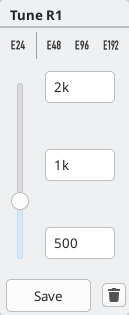
-
The dropdown menu at the top switches between Single Run and Multi Run modes.
-
In Single Run mode, the simulation is run using the tuned value from the middle text field. Each time this value changes, the simulation is re-run with the new value, and the new results replace the old results.
-
In Multi Run mode, the simulation is run multiple times using different values for the tuned value. All runs are plotted simultaneously to show the spread of results. The Steps control sets the number of runs. The minimum is two runs, as the minimum and maximum values of the tuning range are always included.
-
-
The top text field sets the top end of the tuning range. In Multi Run mode, this sets the value for the last simulation run.
-
The bottom text field sets the bottom end of the tuning range. In Multi Run mode, this sets the value for the first simulation run.
-
The middle text field sets the actual component value that is used in the simulation in Single Run mode. This value can also be adjusted using the slider. In Multi Run mode, the middle text field is disabled.
-
The Save button updates the schematic symbol with the tuned value. Until you press the Save button, the schematic symbol will keep its original value. In Multi Run mode, the Save button is disabled because there is no single value to save back to the schematic.
-
单击
 按钮将元件从调整面板中删除并恢复其原始值。
In addition, it is possible to restrict the component values to those from a particular series of Preferred Values — either of the E24, E48, E96 or E192 series. This is particularly useful when it is necessary to restrict component values to commercially available parts.
Saving simulation setups
You can save a simulation setup in a workbook. Workbooks are files that store information about a simulation setup, including which analyses are configured and what their settings are, which signals are plotted for each analysis, user-defined signals, measurements, cursors, and display settings. A workbook can be saved and reloaded later to restore the previously configured settings in a new session. Workbooks can include more than one simulation: for example, it may contain separate tabs for transient, operating point, and AC analyses which you added as you worked.
You can save a workbook using File → Save Workbook and load one using File → Open Workbook. The most recently used workbook is automatically loaded when the simulator is opened.
| Workbooks store simulation setup information, but they do not store simulation results. You can export simulation results to PNG (graphics) or CSV (simulation data values) with File → Export Current Plot as PNG… and File → Export Current Plot as CSV…. To recreate the results of simulations stored in a workbook, select the appropriate analysis tab in the Simulator window and run the simulation again (R or Simulation → Run Simulation). |
Exporting simulation results
KiCad 的仿真器提供了两种导出结果的方式:
-
as a PNG (Portable Network Graphics format) image of a simulation data plot,
-
as a plain text file of simulation data values, in CSV (Comma-Separated Value) format.
Only simulations that produce plots (see above) can be exported as an image or a CSV file. The results of OP and PZ analyses cannot be exported in this way.
Exporting results as graphics
The currently-visible Simulator plot may be exported as a PNG file using the command File → Export Current Plot as PNG….
The size and aspect-ratio of the saved image will match that of the displayed plot in the Simulator.
You can also copy an image of the active plot to the clipboard using File → Export Current Plot to Clipboard, or insert an image of the active plot into the schematic using File → Export Current Plot to Schematic. Exporting a plot to the schematic is equivalent to exporting the plot to the clipboard and then pasting it into the schematic.
Exporting results as numerical data
The currently-visible Simulator plot may be exported as a CSV file using the command File → Export Current Plot as CSV….
The data in the simulation plot is exported as multiple columns. The precise format is dependent upon the analysis type. In general, there will be multiple columns of data, one corresponding to each variable selected for plotting. The first row of the file is a header row, containing the name of the variable in the column (i.e. 'time', 'V(/Vout)1' or similar).
| When exporting to CSV, only variables selected using their Plot checkbox will be included in the exported file. |
| The data in the exported file contains all the data that would be plotted if the entire plot were displayed. If the plot is zoomed in to show a particular region this will still be the case, resulting in the output file containing more data than the user might expect. |
This function exports the data with data separated by semicolons (;) rather than commas. Programs reading this data may need to be configured to expect a semicolon as a delimiter.
|
Troubleshooting simulations
Sometimes a simulation will fail, either with or without errors being reported. Paying attention to the error messages reported, taking care in the development and entry into KiCad of the circuit to be simulated, and making use of the KiCad, ngspice and general SPICE documentation and information from fellow users in forums is very worthwhile and can often point the way to a solution.
It’s worth noting, for users unfamiliar with SPICE, ngspice or circuit simulation in general that some 'common' and interesting circuits can sometimes be tricky to simulate accurately or reliably. These include apparently simple circuits such as oscillators, which in some cases may fail to oscillate at all! It is nearly always possible to build a working simulation but sometimes this can more require SPICE experience than might be initially apparent, or the guidance of someone who already has it. The ngspice documentation, once again, is worth reading for insights into good and effective simulation practices if you are encountering difficulty.
网表不正确
It is possible to inspect the SPICE netlist with Simulation → Show SPICE netlist… (![]() button). This method of troubleshooting requires some SPICE knowledge, but spotting errors in the netlist can help determine the cause of simulation problems, as well as providing confirmation of what input ngspice is actually acting on.
button). This method of troubleshooting requires some SPICE knowledge, but spotting errors in the netlist can help determine the cause of simulation problems, as well as providing confirmation of what input ngspice is actually acting on.
Simulation error messages
The output console displays messages from the simulator. It is advisable to check the console output to verify there are no errors or warnings. Messages appearing in the console may be conveniently selected, copied, and pasted if you wish to share them.
A common error message is "timestep too small". This message means that the simulation engine is unable to calculate the next point in the simulation, even when using the minimum possible time increment. This error can have many causes, including numerical convergence issues with a simulation model used in the circuit or with the circuit itself. It can also be caused by mistakes in drawing the circuit, such as incorrectly assigning pins to the simulation model or forgetting to provide a voltage supply.
收敛问题
In case the simulation does not converge in a reasonable amount of time (or not at all), it is possible to add the following SPICE directives. More information is available in the ngspice manual.
| 更改收敛选项可能会导致错误的结果。 应谨慎使用这些选项。 |
.options gmin=1e-10
.options abstol=1e-10
.options reltol=0.003
.options cshunt=1e-15
-
gminis the minimum conductance allowed by the program. The default value is1e-12(1 pS). -
abstolis the absolute current error tolerance of the program. The default value is1e-12(1 pA). -
reltol是程序的相对容错度。 默认值为0.001(0.1%)。 -
cshuntadds a capacitor of the specified value from each voltage node in the circuit to ground.
Simulation pin assignments
If unexpected results are generated by a simulation despite it running without obvious errors, it is worth double-checking that the assignments between the pins of the part instance in the KiCad schematic and that of the associated model are correct. These have to be correct for each instance of the model in the schematic.
Helpful hints
Some helpful tips, hints and advice to help you get the most from using ngspice in KiCad for simulation.
The ngspice manual is your friend!
Fundamentally the KiCad Simulator is a user-friendly front-end to the powerful ngspice circuit simulator. Therefore problems with the details of simulation, the correct use of SPICE elements, models, etc. is beyond the scope of the KiCad documentation but is very likely to be fully and completely addressed in the ngspice documentation itself. It’s therefore recommended not to overlook this valuable resource.
| KiCad updates may result in changes to the ngspice version used by the simulator. The current version of ngspice used in a particular version of KiCad is shown on the Help → About KiCad dialog, under the Version tab. Referring to the online ngspice documentation will ensure you always have access to the latest information for reference. |
Organizing third-party models
Although it is certainly possible to keep simulation models (i.e. .lib, .sub files) in the directories associated with individual KiCad projects, this will likely result in unnecessary copies of model files proliferating as you create simulations. Consider creating a dedicated storage location (directory, folder) for models, perhaps organized by manufacturer or device type, to hold these files. Then they may simply be referenced in simulations at a common location.
Simulation symbols and models in KiCad’s libraries
The KiCad libraries provide a number of symbols for simulation in the Simulation_SPICE symbol library. Most of these symbols have SPICE models already assigned as appropriate, although you may need to adjust the model parameters in order to obtain the desired simulation behavior.
The Simulation_SPICE symbol library contains the following symbols:
Symbol Name |
描述 |
0 |
A ground (node 0) symbol. Note that a standard GND symbol from another library can also be used. |
BSOURCE |
A symbol for a SPICE B-source (nonlinear dependent voltage or current source). Refer to the ngspice manual for information on B-sources. |
D |
A diode symbol. Note that the pin assignment is appropriate for both simulation and PCB layout. |
ESOURCE |
A symbol for a SPICE E-source (linear voltage-controlled voltage source). By default it is set up with a gain of 1 V/V. Refer to the ngspice manual for more information on E-sources. |
GSOURCE |
A symbol for a SPICE G-source (linear voltage-controlled current source). By default it is set up with a gain of 1 A/V. Refer to the ngspice manual for more information on G-sources. |
IAM |
A symbol for a SPICE amplitude-modulated independent current source. Refer to the ngspice manual for more information on independent current sources. |
IBIS_DEVICE |
An IBIS device symbol representing a digital input pin. This symbol is not preconfigured with a simulation model. It is intended to be used with an external IBIS model for a device. |
IBIS_DEVICE_DIFF |
An IBIS device symbol representing a digital differential input pin. This symbol is not preconfigured with a simulation model. It is intended to be used with an external IBIS model for a differential device. |
IBIS_DRIVER |
An IBIS driver symbol representing a digital output pin. This symbol is not preconfigured with a simulation model. It is intended to be used with an external IBIS model for a driver. |
IBIS_DRIVER_DIFF |
An IBIS driver symbol representing a pair of digital differential output pins. This symbol is not preconfigured with a simulation model. It is intended to be used with an external IBIS model for a differential driver. |
IDC |
A symbol for a SPICE DC independent current source. Refer to the ngspice manual for more information on independent current sources. |
IEXP |
A symbol for a SPICE exponential independent current source. Refer to the ngspice manual for more information on independent current sources. |
IPULSE |
A symbol for a SPICE pulsed independent current source. Refer to the ngspice manual for more information on independent current sources. |
IPWL |
A symbol for a SPICE piecewise linear independent current source. The waveform is specified as space-separated time-current pairs. Refer to the ngspice manual for more information on independent current sources. |
ISFFM |
A symbol for a SPICE single-frequency frequency-modulated independent current source. Refer to the ngspice manual for more information on independent current sources. |
ISIN |
A symbol for a SPICE sinusoidal independent current source. Refer to the ngspice manual for more information on independent current sources. |
ITRNOISE |
A symbol for a SPICE transient noise independent current source. Refer to the ngspice manual for more information on independent current sources. |
ITRRANDOM |
A symbol for a SPICE transient random independent current source. Refer to the ngspice manual for more information on independent current sources. |
NJFET |
A symbol for an N-channel JFET with drain, gate, and source terminals, suitable for use with 3-terminal N-JFET models. |
NMOS |
A symbol for an N-channel MOSFET with drain, gate, and source terminals, suitable for use with 3-terminal N-MOSFET models. |
NMOS_Substrate |
A symbol for an N-channel MOSFET with drain, gate, source, and substrate (bulk) terminals, suitable for use with 4-terminal N-MOSFET models. |
NPN |
A symbol for an NPN transistor with collector, base, and emitter terminals, suitable for use with 3-terminal NPN models. |
NPN_Substrate |
A symbol for an NPN transistor with collector, base, emitter, and substrate terminals, suitable for use with 4-terminal NPN models. |
OPAMP |
A generic single-pole operational amplifier symbol. There are parameters for pole frequency, open loop gain, offset voltage, and output resistance. These parameters can be edited in the Parameters grid of the SPICE Model Editor dialog. |
PJFET |
A symbol for a P-channel JFET with drain, gate, and source terminals, suitable for use with 3-terminal P-JFET models. |
PMOS |
A symbol for a P-channel MOSFET with drain, gate, and source terminals, suitable for use with 3-terminal P-MOSFET models. |
PMOS_Substrate |
A symbol for a P-channel MOSFET with drain, gate, source, and substrate (bulk) terminals, suitable for use with 4-terminal P-MOSFET models. |
PNP |
A symbol for a PNP transistor with collector, base, and emitter terminals, suitable for use with 3-terminal PNP models. |
PNP_Substrate |
A symbol for a PNP transistor with collector, base, emitter, and substrate terminals, suitable for use with 4-terminal PNP models. |
SWITCH |
A symbol for a voltage-controlled switch. Refer to the ngspice manual for more information on switches. |
TLINE |
A symbol for a transmission line. By default it is set up as a lossless transmission line but it can also be used for a lossy transmission line. Refer to the ngspice manual for more information on transmission lines. |
VAM |
A symbol for a SPICE amplitude-modulated independent voltage source. Refer to the ngspice manual for more information on independent voltage sources. |
VDC |
A symbol for a SPICE DC independent voltage source. Refer to the ngspice manual for more information on independent voltage sources. |
VEXP |
A symbol for a SPICE exponential independent voltage source. Refer to the ngspice manual for more information on independent voltage sources. |
VOLTMETER_DIFF |
A differential voltmeter symbol that can be used to measure the voltage
between two arbitrary nodes. The voltage difference between the |
VPULSE |
A symbol for a SPICE pulsed independent voltage source. Refer to the ngspice manual for more information on independent voltage sources. |
VPWL |
A symbol for a SPICE piecewise linear independent voltage source. The waveform is specified as space-separated time-voltage pairs. Refer to the ngspice manual for more information on independent voltage sources. |
VSFFM |
A symbol for a SPICE single-frequency frequency-modulated independent voltage source. Refer to the ngspice manual for more information on independent voltage sources. |
VSIN |
A symbol for a SPICE sinusoidal independent voltage source. Refer to the ngspice manual for more information on independent voltage sources. |
VTRNOISE |
A symbol for a SPICE transient noise independent voltage source. Refer to the ngspice manual for more information on independent voltage sources. |
VTRRANDOM |
A symbol for a SPICE transient random independent voltage source. Refer to the ngspice manual for more information on independent voltage sources. |
Most of these symbols in the Simulation_SPICE library use built-in models, but several symbols use external models from the Simulation_SPICE.sp simulation model library. The simulation model library is a separate file in the same folder as the symbol library. This simulation model library also contains SPICE models that may be useful for use with other symbols.
The Simulation_SPICE.sp simulation model library contains the following models:
Model Name |
描述 |
kicad_builtin_opamp |
A generic single-pole operational amplifier model. This model is used by the
OPAMP symbol in the |
kicad_builtin_opamp_dual |
A dual version of the kicad_builtin_opamp model, with the same parameters.
This model is not assigned to any symbols in the |
kicad_builtin_opamp_quad |
A quad version of the kicad_builtin_opamp model, with the same parameters.
This model is not assigned to any symbols in the |
kicad_builtin_varistor |
A generic varistor model. This model is not assigned to any symbols in the
|
kicad_builtin_vdiff |
A differential voltmeter model. The voltage difference between the first two
terminals is output as a ground-referenced voltage on the third terminal.
This model is used by the VOLTMETER_DIFF symbol in the |
高级主题
配置和定制
| KiCad 文档的这一部分尚未编写。 感谢您的耐心等待,我们的志愿文档编写者正在努力更新和扩展文档。 |
文本变量
KiCad supports text variables, which allow you to reference predefined variables by name in many kinds of text. KiCad will substitute the variable name with the text string assigned to the variable. Text variables can be used in schematic and PCB graphic text, symbol and footprint text, symbol and footprint fields, drawing sheet fields, label names, label fields, hierarchical sheet fields, and other text contexts. This substitution happens anywhere the variable name is used inside the variable replacement syntax of ${VARIABLENAME}.
For example, you could create a variable named VERSION and set the text substitution to 1.0. Now, in any text object in the schematic, you can enter ${VERSION} and KiCad will display this as 1.0. If you change the value to 2.0, every text object that includes ${VERSION} will be updated automatically. You can also mix regular text and variables: a text object with the text Version: ${VERSION} will be displayed as Version: 1.0.
You can define project text variables in the schematic or board setup dialogs. These are referred to as project text variables because they are defined for the whole project, so a project text variable defined in the Schematic Editor can also be used in the Board Editor, and vice versa.
The Schematic Editor also has a number of built-in system text variables, which are listed in the table below. System text variables may be available in some contexts and not others. There is an equivalent list of variables for the PCB Editor.
除非另有说明,否则层次化原理图字段中使用的变量指的是子原理图页的属性,而不是父图的属性。 例如,${#} 在层次化原理图字段中使用时返回子原理图的页码,在父原理图中的图形文本中使用时才返回父原理图的页码。
变量也可用于字段名。以变量作为名称的字段,其值将自动设置为相同的变量。例如,在一个将项目变量 MY_VAR 设为 MY_VALUE`的工程中,用户创建的名为 `${MY_VAR} 的符号字段将自动将其值设为 ${MY_VAR},然后解析为 MY_VALUE。如果设置了字段的 显示名称 属性,变量名称将作为字段名称显示,例如 MY_VAR: MY_VALUE。
| Variable name | 描述 |
|---|---|
|
Sheet number. |
|
Total number of schematic sheets. |
|
Column (letter) and row (zero-indexed number) address of current table cell. This variable is only available in table cells. |
|
Contents of the table cell indexed by |
|
Column number (zero-indexed) of current table cell. This variable is only available in table cells. |
|
Contents of drawing sheet’s |
|
Contents of drawing sheet’s |
|
Today’s date, in ISO format. |
|
The current time, in |
|
The current time, in your current locale’s time format. |
|
Filename of the root schematic sheet, with a file extension. |
|
Full file path of the root schematic sheet, with a file extension. |
|
Contents of drawing sheet’s |
|
Current version of KiCad. This variable is only available in drawing sheet fields. |
|
Current sheet’s paper size. This variable is only available in drawing sheet fields. |
|
Project name, without a file extension. |
|
Contents of drawing sheet’s |
|
Row number (zero-indexed) of current table cell. This variable is only available in table cells. |
|
Filename of the current sheet, with a file extension. |
|
Sheet name of the current sheet. |
|
Sheet path of the current sheet. |
|
Contents of drawing sheet’s |
|
Name of the currently active design variant. Resolves to an empty string when the default variant is active. |
|
Description of the currently active design variant. Resolves to an empty string when the default variant is active or the active variant has no description. |
|
Full hash of the project’s current Git commit. If the project is not part of a Git repository, resolves to "no hash". |
|
Short (8 character) hash of the project’s current Git commit. If the project is not part of a Git repository, resolves to "no hash". |
|
Contents of project text variable
|
|
Contents of symbol field, symbol attribute, hierarchical sheet field, or
label field Both built-in and user-defined fields are available. Built-in fields use all
uppercase letters: for example, to access a symbol’s value, use Built-in symbol fields are
Built-in symbol attributes are
Built-in sheet fields are
Built-in label fields are
|
|
Contents of field or attribute Both built-in and user-defined fields are available. Built-in fields use all
uppercase letters: for example, to access the value of Built-in symbol fields are
Built-in symbol attributes are
Note: If the symbol referenced by |
|
Generates an ERC error named For example, a text item containing |
|
Generates an ERC warning named |
Text expressions
KiCad has a system for evaluating text expressions, which allows you to manipulate text, evaluate mathematical expressions in strings, and dynamically create strings based on other information. Text expressions can be used in schematic and PCB graphic text, symbol and footprint text, symbol and footprint fields, drawing sheet fields, and other text contexts.
Text expressions are evaluated when the @{expression} syntax is used. Everything inside the braces is evaluated, and the entire expression, including the surrounding @{}, is replaced by the evaluated results. If the expression cannot be evaluated, the expression is not replaced and the original text is retained.
As a basic example, a text object containing 1 plus 1 is @{1 + 1} will read 1 plus 1 is 2.
Many expression functions are provided to perform more complex operations. The available expression functions are detailed in the tables below. For example, the absolute value of a number can be calculated using the abs function: @{abs(-1)} evaluates to 1.
A single text item can contain multiple text evaluations, and evaluations can be nested. You can also combine text evaluations with text variables. For example, @{max(1, 2, 3)}, @{max(4, 5, 6)} evaluates to 3, 6. If the text variable var is defined as -10, a text item containing @{max(abs(${var}), 5)} evaluates to 10.
Numbers can be written in scientific notation, so @{2e3 + 1} evaluates to 2001.
Text expressions support units. Results are always printed in SI units, and the unit is not printed. For example, @{1mm + 1in} evaluates to 26.4.
In addition to numbers, some expression functions operate on strings. A string is text that is enclosed with single or double quotes, like 'string 1' or "string 2". An example of an expression function that operates on strings is upper, which converts a string to uppercase. @{upper("string")} evaluates to STRING.
You can concatenate multiple strings or strings and numbers using the concat expression function or using the + operator: @{concat("hello ", "world")} and @{"hello " + "world"} both evaluate to hello world. @{concat("revision ", 1)} and @{"revision " + 1} both evaluate to revision 1.
Mathematical and logical expressions
The following arithmetic operations are available for operations between two numbers. The operators are all infix operators and obey order of operations. Parentheses can be used for grouping. For example, @{3 + 4 * 3} evaluates to 15, and @{(3 + 4) * 3} evaluates to 21.
| Arithmetic operator | 描述 | Example |
|---|---|---|
|
Addition Note: |
|
|
Subtraction |
|
|
Multiplication |
|
|
Division (the expression is not evaluated if the divisor is |
|
|
Modulo (the expression is not evaluated if the divisor is |
|
|
Exponentiation (right-associative) |
|
The following expression functions are available for performing mathematical functions. For example, @{abs(-1)} evaluates to 1.
| Expression function | 描述 | Example |
|---|---|---|
|
Evaluates to the absolute value of |
|
|
Evaluates to the square root of |
|
|
Evaluates to |
|
|
Evaluates to the greatest integer less than or equal to |
|
|
Evaluates to the smallest integer greater than or equal to |
|
|
Evaluates to |
|
|
Evaluates to the minimum of the given comma-separated values. |
|
|
Evaluates to the maximum of the given comma-separated values. |
|
|
Evaluates to the sum of the given comma-separated values. |
|
|
Evaluates to the average of the given comma-separated values. |
|
|
Evaluates to a random number between |
|
|
Evaluates to the equivalent resistance of the two parallel resistances |
|
|
Converts the power ratio |
|
|
Converts the voltage or current ratio |
|
|
Converts the quantity |
|
|
Converts the quantity |
|
|
Evaluates to the closest E-series standard value to |
|
|
Evaluates to the closest E-series standard value greater than |
|
|
Evaluates to the closest E-series standard value less than |
|
Boolean expressions
The following boolean operations are available. These operations evaluate to 1 if the expression is true or 0 if it is false.
| Arithmetic operator | 描述 | Example |
|---|---|---|
|
Less than |
|
|
Less than or equal to |
|
|
Greater than |
|
|
Greater than or equal to |
|
|
Equal to |
|
|
Not equal to |
|
The following expression functions are available for operating on the result of a boolean or mathematical expression.
| Expression function | 描述 | Example |
|---|---|---|
|
Evaluates to |
|
String manipulation
The following expression functions are available for manipulating strings.
Strings are text that is surrounded by single or double quotes.
For example, "this is a string" and 'this is also a string'.
|
| Expression function | 描述 | Example |
|---|---|---|
|
Evaluates to |
|
|
Evaluates to |
|
|
Evaluates to the given comma-separated strings or numbers concatenated together. Note: strings and numbers can also be concatenated using the |
|
|
Evaluates to the portion of |
|
|
Evaluates to the portion of |
|
|
Evaluates to the portion of |
|
|
Evaluates to the portion of |
|
|
Evaluates to |
|
|
Formats Note: |
|
|
Formats Note: |
|
|
Formats |
|
Date and time formatting
The following expression functions are available for manipulating dates and times.
| Expression function | 描述 | Example |
|---|---|---|
|
Evaluates to the current date, represented as the number of days since the Unix epoch (00:00:00 UTC on 1970-01-01). Note: this value can be formatted in various ways using the |
|
|
Evaluates to the current timestamp, represented as the number of seconds since the Unix epoch (00:00:00 UTC on 1970-01-01). Note: you can add or subtract numbers to this value to get timestamps relative to the current timestamp. |
|
|
Formats |
|
|
Evaluates to the day of the week of the date represented by |
|
|
Formats |
|
Version control expressions
The following expression functions are available for extracting version control system information about the project. If the project is not under version control, each expression function evaluates to <unknown>.
Git is the only supported version control system for these expression functions.
| Expression function | 描述 |
|---|---|
|
Evaluates to the current HEAD commit identifier, truncated to |
|
Evaluates to the current branch name. |
|
Evaluates to the current HEAD commit’s author’s name. |
|
Evaluates to the current HEAD commit’s author’s email address. |
|
Evaluates to the current HEAD commit’s committer’s name. |
|
Evaluates to the current HEAD commit’s committer’s email address. |
|
Evaluates to the current HEAD commit’s commit date.
Valid values for |
|
Evaluates to the name of the matching tag closest to the HEAD commit.
|
|
Evaluates to the number of commits between HEAD and the matching tag closest to the HEAD commit.
|
|
Evaluates to |
|
Evaluates to the given |
|
Evaluates to the commit identifier of the last commit that modified the specified |
|
Evaluates to the name of the author of the last commit that modified the specified |
|
Evaluates to the email address of the author of the last commit that modified the specified |
|
Evaluates to the name of the committer of the last commit that modified the specified |
|
Evaluates to the email address of the committer of the last commit that modified the specified |
|
Evaluates to the commit date of the last commit that modified the specified |
数据库关联库文件
数据库关联库是 KiCad 符号库的一种类型,它在外部 SQL 数据库中保存有关零件的数据。 数据基础库本身不包含任何符号或封装的定义。 相反,它们 引用 其他 KiCad 库中的符号和封装。每个数据库关联库文件条目都将一个 KiCad 符号(来自其他库)映射到一组属性(字段),通常还有一个 KiCad 封装(来自封装库)。
使用数据库关联库可以抛开 KiCad 符号库和封装,而创建完全自定义的元件(也可称为 最小元件),而无需在符号库中存储所有元件属性。 外部数据库可以链接到第三方工具,用于管理元件数据和生命周期。 数据库关联库的工作流程通常比标准 KiCad 库的工作流程更复杂,因此这种类型的库通常只用于大规模的元件库,因为完全自定义的元件库可以使得效率提高(这在组织或团队协同中很常见)。
KiCad 不提供编辑 SQL 数据库或定义数据库关联库的图形界面。 用户可以自行寻找最合适的工作流程和工具链来创建并更新数据库。 有些用户可能希望通过第三方数据库客户端直接编辑数据库,有些用户可能使用其他第三方软件,如元件生命周期管理(PLM)工具来创建和编辑数据。
在数据库关联库中,有一个或多个 表,每个表通常代表单一类型的元件(如电阻或电容)。 每个表可以有一个独立的结构,这意味着不同类型的元件可以有不同的属性,这些属性在 KiCad 中被转化为符号字段。 每个表必须有一个唯一的 ID 列,作为从该表放置的符号的标识符。 这个唯一的 ID 通常是一个物料号(制造商零件编号,或内部组织的零件编号)。 每张表还必须有一列包含 KiCad 符号的映射,形式为 LibraryNickname:SymbolName。 LibraryNickname 必须与 KiCad 库表中的符号库相匹配。 表也可以包含一个包含 KiCad 封装的列,形式为 LibraryNickname:FootprintName。 如果这一列存在,从表中放置的符号将包括一个封装映射。
表也可以包含任意的额外列,这些列可以选择性地映射到 KiCad 中的符号字段。 KiCad 数据库关联库的配置文件控制这些字段的命名方式,是否使字段可见,以及是否将字段包含在符号选择器中显示的数据。
数据库关联库配置文件
要创建一个数据库关联库,你必须创建一个配置文件,其中包含 KiCad 连接到你的数据库的必要信息并从表中获取数据。 将下面的模板复制到一个新文件中,并以 kicad_dbl 为扩展名保存。 然后你可以使用配置符号库对话框将此文件添加到你的全局符号库表中。
{
    "meta": {
        "version": 0
    },
    "name": "My Database Library",
    "description": "A database of components",
    "globally_unique_keys": false,
    "source": {
        "type": "odbc",
        "dsn": "",
        "username": "",
        "password": "",
        "timeout_seconds": 2,
        "connection_string": ""
    },
    "libraries": [
        {
            "name": "Resistors",
            "table": "Resistors",
            "key": "Part ID",
            "symbols": "Symbols",
            "footprints": "Footprints",
            "fields": [
                {
                    "column": "MPN",
                    "name": "MPN",
                    "visible_on_add": false,
                    "visible_in_chooser": true,
                    "show_name": true,
                    "inherit_properties": true
                },
                {
                    "column": "Value",
                    "name": "Value",
                    "visible_on_add": true,
                    "visible_in_chooser": true,
                    "show_name": false
                }
            ],
            "properties": {
                "description": "Description",
                "footprint_filters": "Footprint Filters",
                "keywords": "Keywords",
                "exclude_from_bom": "No BOM",
                "exclude_from_board": "Schematic Only"
            }
        }
    ]
}| 数据库库文件采用 JSON 格式。 标准 JSON 语法规则适用。 要检查文件是否包含语法错误,可使用 JSON 验证器或线程(可在线获取)。 |
Configuring top level settings
name: The name of the library.
description: A description of the library.
globally_unique_keys: optional, defaults to false. Controls the format of the library link when placing parts in schematics. If true library link format is LIB_NAME:KEY. If false library link format is LIB_NAME:SUB_LIB_NAME/KEY. If true keys must be unique across all sub-libraries. When enabled this allows parts to be moved between sub-libraries without breaking the link in schematics (useful for library refactors and fixing miscategorized parts). When false keys only need to be unique within each individual sub-library.
Changing globally_unique_keys on an existing library will break library links for parts previously placed in schematics.
|
配置数据源
KiCad 目前只支持 ODBC 连接到 SQL 数据库。 你可以用 DSN 或连接字符串进行连接。 如果提供了 DSN 名称,可选的 username 和 password 字段将被用来连接到 DSN。 如果提供了一个连接字符串,dsn, username, 和 password 字段将被忽略。 连接字符串将直接传递给 ODBC 驱动程序,这样就可以包含 ODBC 驱动程序支持的任何参数。
使用 DSN 连接时,将 connection_string 属性留空或从文件中省略。 使用连接字符串时,应将 dsn、username 和`password` 字段留空或从文件中省略。 连接字符串必须以 `Driver ` 键开头,向 ODBC 管理器指明应使用哪个驱动程序,并可包含其他取决于特定驱动程序的键。 详情请查阅 ODBC 驱动程序的文档。 在配置数据库连接时,您可能还会发现 connectionstrings.com 这样的参考网站很有用。
KiCad 不推荐或认可任何特定的 ODBC 驱动程序或数据库服务器,但经测试可与 Sqlite、MySQL、MariaDB 和 PostgreSQL 兼容。
Windows 用户:在 JSON 引用字符串中包含反斜线字符 (\) 时,必须使用第二个反斜线转义。 如果在连接字符串中包含文件路径,请确保使用双反斜线 (\\)。
|
Flatpak 用户: 您需要安装相应的 ODBC 驱动程序作为 Flatpak 扩展。 您可以通过软件管理器(即 GNOME 软件)中 KiCad 的 "加载项 "部分,或通过命令行进行安装: 为 SQLite 运行 flatpak install org.kicad.KiCad.ODBCDriver.sqliteodbc,为 MariaDB 或 MySQL 运行 flatpak install org.kicad.KiCad.ODBCDriver.mariadb-connector-odbc,或为 PostgreSQL 运行 flatpak install org.kicad.KiCad.ODBCDriver.psqlodbc。
|
Flatpak users: Due to Flatpak sandboxing, a possible way to connect to database servers running on your local machine is via TCP/IP. Make sure that your database server allows TCP/IP connections, then add the required Port parameter to your connection string. For example, add Port=3306; for the default TCP port of MySQL/MariaDB, or Server=localhost;Port=5432; to force PostgreSQL to use a TCP connection to the local server. Using the default UNIX domain socket connections for MySQL, MariaDB, or PostgreSQL is only possible when overriding host file system permissions via flatpak override.
|
配置库
每个数据库关联库可以包含映射到单个数据库表的 "子库"。 配置文件中的 libraries 条目包含一个对象列表,每个对象定义一个库。 每个库必须存在以下设置:
name: 子库(表)的名称,该名称将显示在 KiCad UI 中,并作为前缀包含在该子库的每个符号名称中。 该名称可以包含符号名称的任何有效字符,但正斜杠 (/) 除外,因为斜杠字符将用作子库名称和符号名称之间的分隔符。 如果该字段留空,则不会为该子库中的符号添加前缀。
table: 数据库中的表的名称。
key: 包含唯一键的列名,将用于识别表中的器件。
symbols: 包含 KiCad 符号引用的列名。
footprints: 包含 KiCad 封装引用的列名。
fields: 一个字段定义的列表。 在这里定义的每个字段都会在符号被放置在原理图上时被添加到符号中。 如果源符号中已经定义了一个名称相同的字段,那么数据库表中的值将覆盖源符号中定义的任何值。每个字段定义都可以包含:
column: 应该被映射到一个字段的数据库表列的名称。
name: 要从数据库中填充的 KiCad 字段的名称。
visible_on_add: 如果是 true,当符号被添加时,这个字段将在原理图中可见。如果没有指定这个设置,它将默认为 false。
visible_in_chooser: 如果 true,这个字段将在符号选择器中显示为一个列。如果没有指定这个设置,它将默认为 false。
show_name: 如果是 true,除显示其值之外,该字段的名称将在原理图中显示。 如果没有指定这个设置,将默认为 false。
inherit_properties: 如果是 true,并且源符号中已经存在一个给定的 name 字段,那么只有字段内容将从数据库中更新,其他属性(visible_on_add,show_name 等)将保持源符号中的设置。 如果给定的字段名在源符号中不存在,这个设置将被忽略。 如果没有指定这个设置,它将默认为 false。
properties: 符号属性与数据库列的映射。 所有的属性都是可选的;任何没有在数据库库配置中指定的属性都将从为源符号设置的值中继承下来。 支持以下属性:
description: 符号的描述属性。
footprint_filters: 预留给未来的扩展。
keywords: 符号的关键词属性。
exclude_from_bom: 符号的 "不包括在 BOM 中" 设置。 该列必须是数字类型,并将被视为布尔值(0 代表假,1 代表真)。
exclude_from_board: 符号的 "排除在 PCB 之外" 设置。该列必须是数字类型,并将被当作布尔值(0 代表假,1 代表真)。
exclude_from_sim: The symbol’s "Exclude from simulation" setting. The column named here must be a numeric type, and will be taken as a boolean (0 for false, 1 for true).
数据库列可以被映射到自定义(用户定义的)字段,或某些内置的 KiCad 字段,包括 Value 和 Datasheet。
| KiCad 仅支持文本(字符串)字段。 如果映射包含数值 SQL 数据类型的数据库列,将使用通用转换算法将其转换为字符串,对于非常大或非常小的数字,将转换为科学符号。 用户无法对这种格式转换进行微调,因此如果需要明确控制数字到字符串的转换,应使用新列或视图在数据库中进行转换。 |
使用数据库关联库
创建配置文件并将其添加到符号库表中后,您可以使用符号选择器从数据库表中放置元件。 从数据库关联库中放置的元件可以使用 "从库中更新符号" 功能进行更新,该功能将更新数据库中被改变的任何字段,以及更新源库中被改变的符号。
请注意,数据库表所引用的任何源库也必须存在于符号库表中,这样数据库关联库库才能正常工作。 如果你想把一个库只作为数据库关联库的符号源,你可以通过清除 "管理符号库" 对话框中的 "可见" 复选框将其从符号选择器中隐藏起来。
HTTP Libraries
HTTP libraries are a type of KiCad symbol library that sources data about parts for an external source such as an ERP system. They do not contain any symbol or footprint definitions as standard KiCad libraries do. Instead, they reference symbols and footprints found in other KiCad libraries.
HTTP 库为只读库,支持 REST 或类似 REST 的应用程序接口。
HTTP Library Configuration Files
要创建 HTTP 库,必须创建一个配置文件,其中包含 KiCad 连接到提供库(API)并从中获取数据所需的信息。
将下面的模板复制到一个新文件中,并使用 .kicad_httplib 文件扩展名保存。然后编辑该文件,用自己的值替换 root_url 和 token 值。保存后,使用 "配置符号库 "对话框将此文件添加到全局符号库表中,该对话框可在 "偏好设置"→"管理符号库…" 下找到。
用户可以选择配置两种超时设置。timeout_parts_seconds 设置决定了部件信息的有效期,而 timeout_categories_seconds 设置决定了类别的有效期。默认值分别设置为 60 秒和 600 秒,但如果这两个设置的数据预计将保持不变,用户可以选择更高的值。这将大大加快符号选择器的打开速度。值得注意的是,无论这些超时设置如何,KiCad 都会在首次启动时重新缓存数据。
{
    "meta": {
        "version": 1.0
    },
    "name": "KiCad HTTP Library",
    "description": "A KiCad library sourced from a REST API",
    "source": {
        "type": "REST_API",
        "api_version": "v1",
        "root_url": "http://localhost:8000/kicad-api",
        "token": "usertokendatastring",
        "timeout_parts_seconds": 60,
        "timeout_categories_seconds": 600
    }
}
Authentication
身份验证仅通过 访问令牌 完成。如果 HTTP 库是由外部维护的,用户需要向管理员申请一个有效的令牌。
类别的缓存行为
KiCad 在打开 "符号选择器对话框 " 时会缓存一次所有可用的 "类别"。随后,在服务器端对类别所做的任何更改都不会被 KiCad 检测到,直到用户重新启动程序。这种实现方式旨在节省带宽资源,因为它可以防止 KiCad 在用户每次打开 "符号选择器对话框 " 时都尝试从 API 获取数据。这种连续的数据获取,尤其是在带宽受限的情况下,会严重影响 KiCad 的性能。
服务器响应代码
如果 KiCad 收到 API 错误,它会向用户显示错误信息。有关 API 错误和服务器响应的更多信息,请参阅 dev-docs.kicad.org 上的 API 和绑定部分。
自定义网表和 BOM 格式
KiCad 可以导出各种格式的网表和 BOM,如果需要,用户可以定义新的格式。
导出网表的过程在 netlist export section中描述。BOM 导出在BOM导出章节中描述。
下文描述了如何为一个新的导出格式创建一个导出器。
添加新的网表生成器
新的网表生成器可以通过点击 添加生成器… 按钮添加到 导出网表 对话框中。
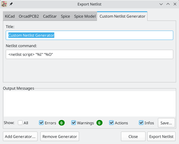
新的生成器需要一个名称和一个命令。名称显示在标签中,只要点击 导出网表 按钮,就会运行该命令。
当网表生成时,KiCad 会创建一个中间的 XML 文件,其中包含原理图中所有的网表信息。然后运行生成器命令,以将中间网表转换为所需的网表格式。
网表命令必须正确设置,以便网表生成器脚本将中间网表文件作为输入并输出所需的网表文件。确切的网表命令将取决于所使用的生成器脚本。下面描述了命令格式。
Python 和 XSLT 是创建自定义网表生成器的常用工具。
添加新的 BOM 生成器
KiCad 还使用中间网表文件,通过 BOM生成工具生成 BOM。
通过点击 ![]() 按钮,可以在 BOM 生成器脚本列表中添加其他脚本。点击
按钮,可以在 BOM 生成器脚本列表中添加其他脚本。点击 ![]() 按钮,可以删除脚本。
按钮,可以删除脚本。![]() 按钮在文本编辑器中打开所选的脚本。
按钮在文本编辑器中打开所选的脚本。
用 Python 和 XSLT 编写的生成器脚本可以包含一个标题注释,描述生成器的功能和用法。这个标题注释会作为每个生成器的描述显示在 BOM 对话框中。标题注释必须包含字符串 @package。该字符串之后直到注释结束的所有内容都被用作生成器的描述。
当添加新的生成器脚本时,KiCad 会自动填充命令行字段,但根据生成器脚本的情况,可能需要手工调整命令行。KiCad 试图从生成器脚本标题中的示例命令行自动确定输出文件扩展名。
生成器命令行格式
网表或 BOM 导出器的命令行定义了 KiCad 将运行的命令,用以生成所选输出文件。
对于使用 xsltproc 的网表导出器,以下为一个示例:
xsltproc -o %O.net /usr/share/kicad/plugins/netlist_form_pads-pcb.asc.xsl %I
对于使用 Python 的 BOM 导出器,以下为一个示例:
/usr/bin/python3 /usr/share/kicad/plugins/bom_csv_grouped_by_value.py "%I" "%O.csv"
建议在命令行中用引号 (") 将参数括起来,以防它们包含空格或其他特殊字符。
|
某些字符序列(如 %I 和 %O)在命令行中具有特殊含义,因为 KiCad 在执行命令之前将它们替换为文件名或路径。
| Parameter | Replaced with… | 描述 |
|---|---|---|
|
|
Absolute path and filename of the intermediate netlist file, which is the input to the BOM or netlist generator plugin |
|
|
Absolute path and filename of the output BOM or netlist file (without file
extension). An appropriate file extension may need to be specified after the
|
|
|
Base filename of the output BOM or netlist file (without path or file
extension). An appropriate file extension may need to be specified after the
|
|
|
Absolute path of the project directory, without trailing slash. |
中间网表文件格式
当输出 BOM 文件和网表时,KiCad 会创建一个中间网表文件,然后运行一个单独的工具,将中间网表后期处理成所需的网表或 BOM 格式。
中间网表使用 XML 语法。它包含有关设计的大量数据。根据输出(BOM 或网表),完整中间网表文件的不同子集将包含在最终输出文件中。
中间网表文件的结构详述 如下。
由于从中间网表文件到输出网表或 BOM 的转换是文本到文本的转换,因此可以使用 Python、XSLT 或任何其他能够将 XML 作为输入的工具编写后处理过滤器。
不建议新的网表或 BOM 导出器使用 XSLT;应该改用 Python 或其他工具。从 KiCad 7 开始,xsltproc 不再随 KiCad 一起安装,尽管它可以单独安装。 不过,下面列出了使用 XSLT 的网表导出器的几个示例。
|
中间网表结构
此示例提供了网表文件格式的概览。
<?xml version="1.0" encoding="utf-8"?>
<export version="D">
  <design>
    <source>F:\kicad_aux\netlist_test\netlist_test.sch</source>
    <date>29/08/2010 21:07:51</date>
    <tool>eeschema (2010-08-28 BZR 2458)-unstable</tool>
  </design>
  <components>
    <comp ref="P1">
      <value>CONN_4</value>
      <libsource lib="conn" part="CONN_4"/>
      <sheetpath names="/" tstamps="/"/>
      <tstamps>4C6E2141</tstamps>
    </comp>
    <comp ref="U2">
      <value>74LS74</value>
      <libsource lib="74xx" part="74LS74"/>
      <sheetpath names="/" tstamps="/"/>
      <tstamps>4C6E20BA</tstamps>
    </comp>
    <comp ref="U1">
      <value>74LS04</value>
      <libsource lib="74xx" part="74LS04"/>
      <sheetpath names="/" tstamps="/"/>
      <tstamps>4C6E20A6</tstamps>
    </comp>
    <comp ref="C1">
      <value>CP</value>
      <libsource lib="device" part="CP"/>
      <sheetpath names="/" tstamps="/"/>
      <tstamps>4C6E2094</tstamps>
    <comp ref="R1">
      <value>R</value>
      <libsource lib="device" part="R"/>
      <sheetpath names="/" tstamps="/"/>
      <tstamps>4C6E208A</tstamps>
    </comp>
  </components>
  <libparts/>
  <libraries/>
  <nets>
    <net code="1" name="GND">
      <node ref="U1" pin="7"/>
      <node ref="C1" pin="2"/>
      <node ref="U2" pin="7"/>
      <node ref="P1" pin="4"/>
    </net>
    <net code="2" name="VCC">
      <node ref="R1" pin="1"/>
      <node ref="U1" pin="14"/>
      <node ref="U2" pin="4"/>
      <node ref="U2" pin="1"/>
      <node ref="U2" pin="14"/>
      <node ref="P1" pin="1"/>
    </net>
    <net code="3" name="">
      <node ref="U2" pin="6"/>
    </net>
    <net code="4" name="">
      <node ref="U1" pin="2"/>
      <node ref="U2" pin="3"/>
    </net>
    <net code="5" name="/SIG_OUT">
      <node ref="P1" pin="2"/>
      <node ref="U2" pin="5"/>
      <node ref="U2" pin="2"/>
    </net>
    <net code="6" name="/CLOCK_IN">
      <node ref="R1" pin="2"/>
      <node ref="C1" pin="1"/>
      <node ref="U1" pin="1"/>
      <node ref="P1" pin="3"/>
    </net>
  </nets>
</export>
通用网表文件结构
中间网表由五个部分组成。
-
“标题” 部分。
-
“元件” 部分。
-
“库元件” 部分。
-
“库” 部分。
-
“网络” 部分。
文件内容带有分隔符 <export>
<export version="D">
...
</export>
“标题”部分
标题带有分隔符 <design>
<design>
<source>F:\kicad_aux\netlist_test\netlist_test.sch</source>
<date>21/08/2010 08:12:08</date>
<tool>eeschema (2010-08-09 BZR 2439)-unstable</tool>
</design>
此部分可视为评论。
“元件”部分
元件部分带有分隔符 <components>
<components>
<comp ref="P1">
<value>CONN_4</value>
<libsource lib="conn" part="CONN_4"/>
<sheetpath names="/" tstamps="/"/>
<tstamps>4C6E2141</tstamps>
</comp>
</components>
本部分包含原理图中的元件列表。 每个元件都是这样描述的:
<comp ref="P1">
<value>CONN_4</value>
<libsource lib="conn" part="CONN_4"/>
<sheetpath names="/" tstamps="/"/>
<tstamps>4C6E2141</tstamps>
</comp>| Element name | Element description |
|---|---|
|
name of the lib where this component was found. |
|
component name inside this library. |
|
path of the sheet inside the hierarchy: identify the sheet within the full schematic hierarchy. |
|
timestamp of the component. |
关于元件时间戳的注意事项
为了识别网表中的元件以及电路板上的元件,时间戳引用作为每个元件的唯一标识。然而,KiCad 提供了一种辅助的方式来识别一个元件,即电路板上的对应封装。在原理图工程中重新标注元件,不会失去元件和其封装之间的联系。
时间戳是原理图工程中每个元件或图纸的唯一标识符。但是, 在复杂的层次结构中, 同一个图纸会被多次使用, 因此该图纸包含具有相同时间戳的元件。
在一个复杂的层次结构中,一个给定的图纸有一个唯一的标识符:它的图纸路径。一个给定的元件(在一个复杂的层次结构内)有一个唯一的标识符:图纸路径和它的时间戳。
“库文件”部分
库文件部分带有分隔符 <libparts> 该部分的内容在原理图库中定义。
<libparts>
<libpart lib="device" part="CP">
  <description>Condensateur polarise</description>
  <footprints>
    <fp>CP*</fp>
    <fp>SM*</fp>
  </footprints>
  <fields>
    <field name="Reference">C</field>
    <field name="Valeur">CP</field>
  </fields>
  <pins>
    <pin num="1" name="1" type="passive"/>
    <pin num="2" name="2" type="passive"/>
  </pins>
</libpart>
</libparts>| Element name | Element description |
|---|---|
|
The symbol’s footprint filters. Each footprint filter is in a separate |
|
The symbol’s fields. Each field’s name and value is given in a separate `<field name="fieldname">…</field> tag. |
|
The symbol’s pins. Each pin is given in a separate |
可能的电气引脚类型有:
| Pintype | 描述 |
|---|---|
Input |
Usual input pin |
Output |
Usual output |
Bidirectional |
Input or Output |
Tri-state |
Bus input/output |
无源 |
Usual ends of passive components |
Unspecified |
Unknown electrical type |
Power input |
Power input of a component |
Power output |
Power output like a regulator output |
Open collector |
Open collector often found in analog comparators |
Open emitter |
Open emitter sometimes found in logic |
Not connected |
Must be left open in schematic |
库部分
库部分带有分隔符 <libraries>。该部分包含工程中使用的原理图库的列表。
<libraries>
  <library logical="device">
    <uri>F:\kicad\share\library\device.lib</uri>
  </library>
  <library logical="conn">
    <uri>F:\kicad\share\library\conn.lib</uri>
  </library>
</libraries>
“网络” 部分
网络部分的分隔符为 <nets>。这一部分通过列出所有的网络和连接到每个网络的引脚来描述原理图的连接性。
<nets>
  <net code="1" name="GND">
    <node ref="U1" pin="7"/>
    <node ref="C1" pin="2"/>
    <node ref="U2" pin="7"/>
    <node ref="P1" pin="4"/>
  </net>
  <net code="2" name="VCC">
    <node ref="R1" pin="1"/>
    <node ref="U1" pin="14"/>
    <node ref="U2" pin="4"/>
    <node ref="U2" pin="1"/>
    <node ref="U2" pin="14"/>
    <node ref="P1" pin="1"/>
  </net>
</nets>
一个网络可能包含以下内容。
<net code="1" name="GND">
  <node ref="U1" pin="7"/>
  <node ref="C1" pin="2"/>
  <node ref="U2" pin="7"/>
  <node ref="P1" pin="4"/>
</net>| Element name | Element Description |
|---|---|
|
an internal identifier for this net |
|
the net name |
|
the pin (identified by |
网表导出器实例
下面包括一些使用 XSLT 的网表导出器的例子。
XSLT 本身是一种 XML 语言,非常适用于 XML 转换。 xsltproc 程序 可以用来读取中间的 XML 网表输入文件,应用样式表来转换输入,并将结果保存在输出文件中。使用 xsltproc 需要一个使用 XSLT 惯例的样式表文件。整个转换过程由 KiCad 处理,在它被配置为以特定方式运行 xsltproc 之后。
描述 XSL 变换(XSLT)的文件可在此获得: http://www.w3.org/TR/xslt
| 当编写一个新的网表导出器时,考虑使用 Python 或其他工具而不是 XSLT。 |
使用 XSLT 的 PADS 网表实例
下面的例子显示了如何使用 xlstproc 为 PADS 网表格式创建一个输出器。
PADS 网表格式由两部分组成:
-
封装列表
-
一个网络的列表,以及与每个网络相连的焊盘。
下面是一个 XSL 样式表,将中间网表文件转换为 PADS 网表格式。
<?xml version="1.0" encoding="ISO-8859-1"?>
<!--XSL style sheet to Eeschema Generic Netlist Format to PADS netlist format
Copyright (C) 2010, SoftPLC Corporation.
GPL v2.
如何使用:
https://lists.launchpad.net/kicad-developers/msg05157.html
-->
<!DOCTYPE xsl:stylesheet [
<!ENTITY nl "
"> <!--new line CR, LF -->
]>
<xsl:stylesheet version="1.0" xmlns:xsl="http://www.w3.org/1999/XSL/Transform">
<xsl:output method="text" omit-xml-declaration="yes" indent="no"/>
<xsl:template match="/export">
<xsl:text>*PADS-PCB*&nl;*PART*&nl;</xsl:text>
<xsl:apply-templates select="components/comp"/>
<xsl:text>&nl;*NET*&nl;</xsl:text>
<xsl:apply-templates select="nets/net"/>
<xsl:text>*END*&nl;</xsl:text>
</xsl:template>
<!-- for each component -->
<xsl:template match="comp">
<xsl:text> </xsl:text>
<xsl:value-of select="@ref"/>
<xsl:text> </xsl:text>
<xsl:choose>
<xsl:when test = "footprint != '' ">
<xsl:apply-templates select="footprint"/>
</xsl:when>
<xsl:otherwise>
<xsl:text>unknown</xsl:text>
</xsl:otherwise>
</xsl:choose>
<xsl:text>&nl;</xsl:text>
</xsl:template>
<!-- for each net -->
<xsl:template match="net">
<!-- nets are output only if there is more than one pin in net -->
<xsl:if test="count(node)>1">
<xsl:text>*SIGNAL* </xsl:text>
<xsl:choose>
<xsl:when test = "@name != '' ">
<xsl:value-of select="@name"/>
</xsl:when>
<xsl:otherwise>
<xsl:text>N-</xsl:text>
<xsl:value-of select="@code"/>
</xsl:otherwise>
</xsl:choose>
<xsl:text>&nl;</xsl:text>
<xsl:apply-templates select="node"/>
</xsl:if>
</xsl:template>
<!-- for each node -->
<xsl:template match="node">
<xsl:text> </xsl:text>
<xsl:value-of select="@ref"/>
<xsl:text>.</xsl:text>
<xsl:value-of select="@pin"/>
<xsl:text>&nl;</xsl:text>
</xsl:template>
</xsl:stylesheet>这是运行 xsltproc 后的 PADS 网表输出文件:
*PADS-PCB*
*PART*
P1 unknown
U2 unknown
U1 unknown
C1 unknown
R1 unknown
*NET*
*SIGNAL* GND
U1.7
C1.2
U2.7
P1.4
*SIGNAL* VCC
R1.1
U1.14
U2.4
U2.1
U2.14
P1.1
*SIGNAL* N-4
U1.2
U2.3
*SIGNAL* /SIG_OUT
P1.2
U2.5
U2.2
*SIGNAL* /CLOCK_IN
R1.2
C1.1
U1.1
P1.3

*END*
进行这种转换的命令行是:
kicad\\bin\\xsltproc.exe -o test.net kicad\\bin\\plugins\\netlist_form_pads-pcb.xsl test.tmp
使用 XSLT 的 Cadstar 网表例子
下面的例子显示了如何使用 xlstproc 为 Cadstar 网表格式创建一个输出器。
Cadstar 的格式由两部分组成:
-
封装列表
-
网络列表:按网络对焊盘进行分组
下面是一个 XSL 样式表,将中间网表文件转换为 Cadstar 网表格式。
<?xml version="1.0" encoding="ISO-8859-1"?>
<!--XSL style sheet to Eeschema Generic Netlist Format to CADSTAR netlist format
Copyright (C) 2010, Jean-Pierre Charras.
Copyright (C) 2010, SoftPLC Corporation.
GPL v2. -->
<!DOCTYPE xsl:stylesheet [
<!ENTITY nl "
"> <!--new line CR, LF -->
]>
<xsl:stylesheet version="1.0" xmlns:xsl="http://www.w3.org/1999/XSL/Transform">
<xsl:output method="text" omit-xml-declaration="yes" indent="no"/>
<!-- Netlist header -->
<xsl:template match="/export">
<xsl:text>.HEA&nl;</xsl:text>
<xsl:apply-templates select="design/date"/> <!-- Generate line .TIM <time> -->
<xsl:apply-templates select="design/tool"/> <!-- Generate line .APP <eeschema version> -->
<xsl:apply-templates select="components/comp"/> <!-- Generate list of components -->
<xsl:text>&nl;&nl;</xsl:text>
<xsl:apply-templates select="nets/net"/> <!-- Generate list of nets and connections -->
<xsl:text>&nl;.END&nl;</xsl:text>
</xsl:template>
<!-- Generate line .TIM 20/08/2010 10:45:33 -->
<xsl:template match="tool">
<xsl:text>.APP "</xsl:text>
<xsl:apply-templates/>
<xsl:text>"&nl;</xsl:text>
</xsl:template>
<!-- Generate line .APP "eeschema (2010-08-17 BZR 2450)-unstable" -->
<xsl:template match="date">
<xsl:text>.TIM </xsl:text>
<xsl:apply-templates/>
<xsl:text>&nl;</xsl:text>
</xsl:template>
<!-- for each component -->
<xsl:template match="comp">
<xsl:text>.ADD_COM </xsl:text>
<xsl:value-of select="@ref"/>
<xsl:text> </xsl:text>
<xsl:choose>
<xsl:when test = "value != '' ">
<xsl:text>"</xsl:text> <xsl:apply-templates select="value"/> <xsl:text>"</xsl:text>
</xsl:when>
<xsl:otherwise>
<xsl:text>""</xsl:text>
</xsl:otherwise>
</xsl:choose>
<xsl:text>&nl;</xsl:text>
</xsl:template>
<!-- for each net -->
<xsl:template match="net">
<!-- nets are output only if there is more than one pin in net -->
<xsl:if test="count(node)>1">
<xsl:variable name="netname">
<xsl:text>"</xsl:text>
<xsl:choose>
<xsl:when test = "@name != '' ">
<xsl:value-of select="@name"/>
</xsl:when>
<xsl:otherwise>
<xsl:text>N-</xsl:text>
<xsl:value-of select="@code"/>
</xsl:otherwise>
</xsl:choose>
<xsl:text>"&nl;</xsl:text>
</xsl:variable>
<xsl:apply-templates select="node" mode="first"/>
<xsl:value-of select="$netname"/>
<xsl:apply-templates select="node" mode="others"/>
</xsl:if>
</xsl:template>
<!-- for each node -->
<xsl:template match="node" mode="first">
<xsl:if test="position()=1">
<xsl:text>.ADD_TER </xsl:text>
<xsl:value-of select="@ref"/>
<xsl:text>.</xsl:text>
<xsl:value-of select="@pin"/>
<xsl:text> </xsl:text>
</xsl:if>
</xsl:template>
<xsl:template match="node" mode="others">
<xsl:choose>
<xsl:when test='position()=1'>
</xsl:when>
<xsl:when test='position()=2'>
<xsl:text>.TER </xsl:text>
</xsl:when>
<xsl:otherwise>
<xsl:text> </xsl:text>
</xsl:otherwise>
</xsl:choose>
<xsl:if test="position()>1">
<xsl:value-of select="@ref"/>
<xsl:text>.</xsl:text>
<xsl:value-of select="@pin"/>
<xsl:text>&nl;</xsl:text>
</xsl:if>
</xsl:template>
</xsl:stylesheet>这是 Cadstar 输出文件。
.HEA
.TIM 21/08/2010 08:12:08
.APP "eeschema (2010-08-09 BZR 2439)-unstable"
.ADD_COM P1 "CONN_4"
.ADD_COM U2 "74LS74"
.ADD_COM U1 "74LS04"
.ADD_COM C1 "CP"
.ADD_COM R1 "R"


.ADD_TER U1.7 "GND"
.TER     C1.2
         U2.7
         P1.4
.ADD_TER R1.1 "VCC"
.TER     U1.14
         U2.4
         U2.1
         U2.14
         P1.1
.ADD_TER U1.2 "N-4"
.TER     U2.3
.ADD_TER P1.2 "/SIG_OUT"
.TER     U2.5
         U2.2
.ADD_TER R1.2 "/CLOCK_IN"
.TER     C1.1
         U1.1
         P1.3

.END
使用 XSLT 的 OrcadPCB2 网表示例
这种格式只有一个部分,就是封装列表。每个封装都包括其焊盘的列表,并引用一个网络。
下面是一个 XSL 样式表,将中间网表文件转换为 Orcad 网表格式。
<?xml version="1.0" encoding="ISO-8859-1"?>
<!--XSL style sheet to Eeschema Generic Netlist Format to CADSTAR netlist format
Copyright (C) 2010, SoftPLC Corporation.
GPL v2.
如何使用:
https://lists.launchpad.net/kicad-developers/msg05157.html
-->
<!DOCTYPE xsl:stylesheet [
<!ENTITY nl "
"> <!--new line CR, LF -->
]>
<xsl:stylesheet version="1.0" xmlns:xsl="http://www.w3.org/1999/XSL/Transform">
<xsl:output method="text" omit-xml-declaration="yes" indent="no"/>
<!--
Netlist header
Creates the entire netlist
(can be seen as equivalent to main function in C
-->
<xsl:template match="/export">
<xsl:text>( { Eeschema Netlist Version 1.1 </xsl:text>
<!-- Generate line .TIM <time> -->
<xsl:apply-templates select="design/date"/>
<!-- Generate line eeschema version ... -->
<xsl:apply-templates select="design/tool"/>
<xsl:text>}&nl;</xsl:text>
<!-- Generate the list of components -->
<xsl:apply-templates select="components/comp"/> <!-- Generate list of components -->
<!-- end of file -->
<xsl:text>)&nl;*&nl;</xsl:text>
</xsl:template>
<!--
Generate id in header like "eeschema (2010-08-17 BZR 2450)-unstable"
-->
<xsl:template match="tool">
<xsl:apply-templates/>
</xsl:template>
<!--
Generate date in header like "20/08/2010 10:45:33"
-->
<xsl:template match="date">
<xsl:apply-templates/>
<xsl:text>&nl;</xsl:text>
</xsl:template>
<!--
This template read each component
(path = /export/components/comp)
creates lines:
( 3EBF7DBD $noname U1 74LS125
... pin list ...
)
and calls "create_pin_list" template to build the pin list
-->
<xsl:template match="comp">
<xsl:text> ( </xsl:text>
<xsl:choose>
<xsl:when test = "tstamp != '' ">
<xsl:apply-templates select="tstamp"/>
</xsl:when>
<xsl:otherwise>
<xsl:text>00000000</xsl:text>
</xsl:otherwise>
</xsl:choose>
<xsl:text> </xsl:text>
<xsl:choose>
<xsl:when test = "footprint != '' ">
<xsl:apply-templates select="footprint"/>
</xsl:when>
<xsl:otherwise>
<xsl:text>$noname</xsl:text>
</xsl:otherwise>
</xsl:choose>
<xsl:text> </xsl:text>
<xsl:value-of select="@ref"/>
<xsl:text> </xsl:text>
<xsl:choose>
<xsl:when test = "value != '' ">
<xsl:apply-templates select="value"/>
</xsl:when>
<xsl:otherwise>
<xsl:text>"~"</xsl:text>
</xsl:otherwise>
</xsl:choose>
<xsl:text>&nl;</xsl:text>
<xsl:call-template name="Search_pin_list" >
<xsl:with-param name="cmplib_id" select="libsource/@part"/>
<xsl:with-param name="cmp_ref" select="@ref"/>
</xsl:call-template>
<xsl:text> )&nl;</xsl:text>
</xsl:template>
<!--
This template search for a given lib component description in list
lib component descriptions are in /export/libparts,
and each description start at ./libpart
We search here for the list of pins of the given component
This template has 2 parameters:
"cmplib_id" (reference in libparts)
"cmp_ref" (schematic reference of the given component)
-->
<xsl:template name="Search_pin_list" >
<xsl:param name="cmplib_id" select="0" />
<xsl:param name="cmp_ref" select="0" />
<xsl:for-each select="/export/libparts/libpart">
<xsl:if test = "@part = $cmplib_id ">
<xsl:apply-templates name="build_pin_list" select="pins/pin">
<xsl:with-param name="cmp_ref" select="$cmp_ref"/>
</xsl:apply-templates>
</xsl:if>
</xsl:for-each>
</xsl:template>
<!--
This template writes the pin list of a component
from the pin list of the library description
The pin list from library description is something like
<pins>
<pin num="1" type="passive"/>
<pin num="2" type="passive"/>
</pins>
Output pin list is ( <pin num> <net name> )
something like
( 1 VCC )
( 2 GND )
-->
<xsl:template name="build_pin_list" match="pin">
<xsl:param name="cmp_ref" select="0" />
<!-- write pin numner and separator -->
<xsl:text> ( </xsl:text>
<xsl:value-of select="@num"/>
<xsl:text> </xsl:text>
<!-- search net name in nets section and write it: -->
<xsl:variable name="pinNum" select="@num" />
<xsl:for-each select="/export/nets/net">
<!-- net name is output only if there is more than one pin in net
else use "?" as net name, so count items in this net
-->
<xsl:variable name="pinCnt" select="count(node)" />
<xsl:apply-templates name="Search_pin_netname" select="node">
<xsl:with-param name="cmp_ref" select="$cmp_ref"/>
<xsl:with-param name="pin_cnt_in_net" select="$pinCnt"/>
<xsl:with-param name="pin_num"> <xsl:value-of select="$pinNum"/>
</xsl:with-param>
</xsl:apply-templates>
</xsl:for-each>
<!-- close line -->
<xsl:text> )&nl;</xsl:text>
</xsl:template>
<!--
This template writes the pin netname of a given pin of a given component
from the nets list
The nets list description is something like
<nets>
<net code="1" name="GND">
<node ref="J1" pin="20"/>
<node ref="C2" pin="2"/>
</net>
<net code="2" name="">
<node ref="U2" pin="11"/>
</net>
</nets>
This template has 2 parameters:
"cmp_ref" (schematic reference of the given component)
"pin_num" (pin number)
-->
<xsl:template name="Search_pin_netname" match="node">
<xsl:param name="cmp_ref" select="0" />
<xsl:param name="pin_num" select="0" />
<xsl:param name="pin_cnt_in_net" select="0" />
<xsl:if test = "@ref = $cmp_ref ">
<xsl:if test = "@pin = $pin_num">
<!-- net name is output only if there is more than one pin in net
else use "?" as net name
-->
<xsl:if test = "$pin_cnt_in_net>1">
<xsl:choose>
<!-- if a net has a name, use it,
else build a name from its net code
-->
<xsl:when test = "../@name != '' ">
<xsl:value-of select="../@name"/>
</xsl:when>
<xsl:otherwise>
<xsl:text>$N-0</xsl:text><xsl:value-of select="../@code"/>
</xsl:otherwise>
</xsl:choose>
</xsl:if>
<xsl:if test = "$pin_cnt_in_net <2">
<xsl:text>?</xsl:text>
</xsl:if>
</xsl:if>
</xsl:if>
</xsl:template>
</xsl:stylesheet>这是 OrcadPCB2 输出文件。
( { Eeschema Netlist Version 1.1  29/08/2010 21:07:51
eeschema (2010-08-28 BZR 2458)-unstable}
 ( 4C6E2141 $noname P1 CONN_4
  (  1 VCC )
  (  2 /SIG_OUT )
  (  3 /CLOCK_IN )
  (  4 GND )
 )
 ( 4C6E20BA $noname U2 74LS74
  (  1 VCC )
  (  2 /SIG_OUT )
  (  3 N-04 )
  (  4 VCC )
  (  5 /SIG_OUT )
  (  6 ? )
  (  7 GND )
  (  14 VCC )
 )
 ( 4C6E20A6 $noname U1 74LS04
  (  1 /CLOCK_IN )
  (  2 N-04 )
  (  7 GND )
  (  14 VCC )
 )
 ( 4C6E2094 $noname C1 CP
  (  1 /CLOCK_IN )
  (  2 GND )
 )
 ( 4C6E208A $noname R1 R
  (  1 VCC )
  (  2 /CLOCK_IN )
 )
)
*
操作参考
以下是 KiCad 原理图编辑器中可用 操作 的列表:您可以为以下命令设置快捷键。
原理图编辑器
以下操作在原理图编辑器中可用。可以在偏好设置的 快捷键 部分中将快捷键分配给这些操作中的任何一个。
| Action | Default Hotkey | 描述 |
|---|---|---|
Align to Bottom |
Aligns selected items to the bottom edge of the item under the cursor |
|
Align to Horizontal Center |
Aligns selected items to the horizontal center of the item under the cursor |
|
Align to Vertical Center |
Aligns selected items to the vertical center of the item under the cursor |
|
Align to Left |
Aligns selected items to the left edge of the item under the cursor |
|
Align to Right |
Aligns selected items to the right edge of the item under the cursor |
|
Align to Top |
Aligns selected items to the top edge of the item under the cursor |
|
Align Items to Grid |
||
Add Design Variant… |
Add new design variant to the schematic. |
|
Annotate Schematic… |
Fill in schematic symbol reference designators |
|
Annotate Automatically |
Toggle automatic annotation of new symbols |
|
Assign Footprints… |
Run footprint assignment tool |
|
Clear Net Highlighting |
~ |
Clear any existing net highlighting |
Export Drawing to Clipboard |
Export drawing of current sheet to clipboard |
|
Edit Library Symbol… |
Ctrl+Shift+E |
Open the library symbol in the Symbol Editor |
Edit Sheet Page Number… |
Edit the page number of the current or selected sheet |
|
Bulk Edit Symbol Fields… |
Edit a table of fields from all symbols in the schematic |
|
Bulk Edit Symbol Library Links… |
Edit a table of links between schematic and library symbols |
|
Edit with Symbol Editor |
Ctrl+E |
Open the selected symbol in the Symbol Editor |
Export Netlist… |
Export file containing netlist in one of several formats |
|
Export Symbols… |
Add symbols from schematic to a new or an existing symbol library (does not remove other symbols from this library) |
|
Generate Bill of Materials… |
Generate a bill of materials for the current schematic |
|
Generate Bill of Materials (External)… |
Generate a bill of materials for the current schematic using external generator |
|
Generate Legacy Bill of Materials… |
Generate a bill of materials for the current schematic (Legacy Generator) |
|
Highlight Net |
` |
Highlight net under cursor |
Highlight Nets |
Highlight wires and pins of a net |
|
Import Footprint Assignments… |
Import symbol footprint assignments from .cmp file created by board editor |
|
Import Graphics… |
Ctrl+Shift+F |
Import 2D drawing file |
Increment Annotations From… |
Increment a subset of reference designators starting at a particular symbol |
|
Line Mode for Wires and Buses |
Constrain drawing and dragging to horizontal, vertical, or 45-degree angle motions |
|
Line Mode for Wires and Buses |
Draw and drag at any angle |
|
Line Mode for Wires and Buses |
Shift+Space |
Switch to next angle snapping mode |
Line Mode for Wires and Buses |
Constrain drawing and dragging to horizontal or vertical motions |
|
Mark items excluded from simulation |
Draw 'X’s over items which have been excluded from simulation |
|
Next Net Item |
Tab |
Select next item on the current net |
Next Symbol Unit |
Open the next unit of the symbol |
|
Previous Net Item |
Shift+Tab |
Select previous item on the current net |
Previous Symbol Unit |
Open the previous unit of the symbol |
|
Remap Legacy Library Symbols… |
Remap library symbol references in legacy schematics to the symbol library table |
|
Remove Design Variant… |
Remove an existing design variant from the schematic. |
|
Rescue Symbols… |
Find old symbols in project and rename/rescue them |
|
Save Current Sheet Copy As… |
Save a copy of the current sheet to another location or name |
|
Schematic Setup… |
Edit schematic setup including annotation styles and electrical rules |
|
Select on PCB |
Select corresponding items in PCB editor |
|
Do not Populate |
Set the do not populate attribute |
|
Exclude from Bill of Materials |
Set the exclude from bill of materials attribute |
|
Exclude from Board |
Set the exclude from board attribute |
|
Exclude from Simulation |
Set the exclude from simulation attribute |
|
Show Directive Labels |
||
Show ERC Errors |
Show markers for electrical rules checker errors |
|
Show ERC Exclusions |
Show markers for excluded electrical rules checker violations |
|
Show ERC Warnings |
Show markers for electrical rules checker warnings |
|
Show Hidden Fields |
||
Show Hidden Pins |
||
Net Navigator |
Show/hide the net navigator |
|
Show OP Currents |
Show operating point current data from simulation |
|
Show OP Voltages |
Show operating point voltage data from simulation |
|
Switch to PCB Editor |
Open PCB in board editor |
|
仿真器 |
Show simulation window for running SPICE or IBIS simulations. |
|
Show Pin Alternate Icons |
Show indicator icons for pins with alternate modes |
|
Hierarchy Navigator |
Ctrl+H |
Show/hide the schematic sheet hierarchy navigator |
Symbol Checker |
Show the symbol checker window |
|
Compare Symbol with Library |
Show differences between schematic symbol and its library equivalent |
|
Electrical Rules Checker |
Show the electrical rules checker window |
|
Show Bus Syntax Help |
||
Decrement Primary |
Decrement the primary field of the selected item(s) |
|
Decrement Secondary |
Decrement the secondary field of the selected item(s) |
|
Increment |
Increment the selected item(s) |
|
Increment Primary |
Increment the primary field of the selected item(s) |
|
Increment Secondary |
Increment the secondary field of the selected item(s) |
|
Autoplace All Sheet Pins |
Imports and auto places all sheet pins |
|
Close Outline |
Close the in-progress outline |
|
Delete Last Point |
Delete the last point added to the current item |
|
Draw Arcs |
||
Draw Bezier Curve |
||
Draw Circles |
||
Draw Rectangles |
||
Draw Rule Areas |
||
Draw Hierarchical Sheets |
S |
|
Draw Sheet from Design Block |
Copy design block into project as a sheet on current sheet |
|
Draw Sheet from File |
Copy sheet into project and draw on current sheet |
|
Draw Tables |
||
Draw Text Boxes |
||
Import Sheet… |
Import sheet into project |
|
Place Wire to Bus Entries |
Z |
|
Place Directive Labels |
||
Place Design Block |
Shift+B |
Add selected design block to current sheet |
Place Global Labels |
Ctrl+L |
|
Place Hierarchical Labels |
H |
|
Place Images |
||
Place Junctions |
J |
|
Place Net Labels |
L |
|
Place Linked Design Block |
Place design block linked to selected group |
|
Place Next Symbol Unit |
Place the next unit of the current symbol that is missing from the schematic |
|
Place No Connect Flags |
Q |
|
Place Power Symbols |
P |
|
Draw Text |
T |
|
Place Pins from Sheet |
Add sheet pins from existing hierarchical labels found on that sheet |
|
Place Symbols |
A |
|
Save to Linked Design Block |
Save selected group to linked design block |
|
Sync All Sheet Pins… |
Synchronize all sheet pins and hierarchical labels |
|
Sync Selected Sheet Pins… |
Synchronize selected sheet pins and hierarchical labels |
|
Draw Buses |
B |
|
Draw Lines |
I |
|
Draw Wires |
W |
|
Switch Segment Posture |
/ |
Switches posture of the current segment. |
Undo Last Segment |
Back |
Walks the current line back one segment. |
Unfold from Bus |
C |
Break a wire out of a bus |
Assign Netclass… |
Assign a netclass to nets matching a pattern |
|
Autoplace Fields |
O |
Runs the automatic placement algorithm on the symbol’s (or sheet’s) fields |
Break |
Divide into connected segments |
|
Change Symbol… |
Assign a different symbol from the library |
|
Change Symbols… |
Assign different symbols from the library |
|
Cleanup Sheet Pins |
Delete unreferenced sheet pins |
|
Convert Stacked Pins |
Convert multiple pins at the same location to a single pin with stacked notation |
|
Edit Footprint… |
F |
|
Edit Reference Designator… |
U |
|
Edit Text & Graphics Properties… |
Edit text and graphics properties globally across schematic |
|
Edit Value… |
V |
|
Explode Stacked Pin |
Convert a pin with stacked notation to multiple individual pins |
|
Find in Net Navigator |
Locate the selected net in the net navigator |
|
Mirror Horizontally |
X |
Flips selected item(s) from left to right |
Mirror Vertically |
Y |
Flips selected item(s) from top to bottom |
Pin Table… |
Displays pin table for bulk editing of pins |
|
Properties… |
E |
|
Repeat Last Item |
Ins |
Duplicates the last drawn item |
Rotate Counterclockwise |
R |
|
Rotate Clockwise |
Shift+R |
|
Slice |
Divide into unconnected segments |
|
Swap |
Alt+S |
Swap positions of selected items |
Swap Pin Labels |
Swap the labels attached to selected pins |
|
Swap Pins |
Swap the selected symbol pins' positions |
|
Swap Unit Labels |
Swap labels between selected units |
|
Symbol Properties… |
||
Change to Directive Label |
Change existing item to a directive label |
|
Change to Global Label |
Change existing item to a global label |
|
Change to Hierarchical Label |
Change existing item to a hierarchical label |
|
Change to Label |
Change existing item to a label |
|
Change to Text |
Change existing item to a text comment |
|
Change to Text Box |
Change existing item to a text box |
|
Cycle Body Style |
Switch between De Morgan (or other) representations |
|
Update Symbol… |
Update symbol to include any changes from the library |
|
Update Symbols from Library… |
Update symbols to include any changes from the library |
|
Drag |
G |
Move items while keeping their connections |
Move |
M |
|
Select/Expand Connection |
Ctrl+4 |
Selects a connection or expands an existing selection to pins, symbols, or entire connections |
Select Node |
Alt+3 |
Select a connection item under the cursor |
Navigate Back |
Alt+Left |
Move backward in sheet navigation history |
Change Sheet |
Change to provided sheet’s contents in the schematic editor |
|
Enter Sheet |
Display the selected sheet’s contents in the schematic editor |
|
Navigate Forward |
Alt+Right |
Move forward in sheet navigation history |
Leave Sheet |
Alt+Back |
Display the parent sheet in the schematic editor |
Next Sheet |
PgDn |
Move to next sheet by number |
Previous Sheet |
PgUp |
Move to previous sheet by number |
Navigate Up |
Alt+Up |
Navigate up one sheet in the hierarchy |
Push Pin Length |
Copy pin length to other pins in symbol |
|
Push Pin Name Size |
Copy pin name size to other pins in symbol |
|
Push Pin Number Size |
Copy pin number size to other pins in symbol |
|
Create Corner |
||
Remove Corner |
||
Remote Symbols |
Show/hide the remote symbol panel |
|
Delete Design Block |
Remove the selected design block from its library |
|
Properties… |
Edit properties of design block |
|
Save Selection as Design Block… |
Create a new design block from the current selection |
|
Save Current Sheet as Design Block… |
Create a new design block from the current sheet |
|
Design Blocks |
Show/hide design blocks library |
|
Update Design Block from Selection |
Set design block schematic to current selection |
|
Update Design Block from Current Sheet |
Set design block schematic to current sheet |
|
User-defined Signals… |
Add, edit or delete user-defined simulation signals |
|
New Analysis Tab… |
Ctrl+N |
Create a new tab containing a simulation analysis |
Open Workbook… |
Ctrl+O |
Open a saved set of analysis tabs and settings |
Probe Schematic… |
Shift+P |
Add a simulator probe |
Run Simulation |
R |
|
Save Workbook |
Ctrl+S |
Save the current set of analysis tabs and settings |
Save Workbook As… |
Ctrl+Shift+S |
Save the current set of analysis tabs and settings to another location |
Show SPICE Netlist |
||
Edit Analysis Tab… |
Edit the current analysis tab’s SPICE command and plot setup |
|
Stop Simulation |
||
Add Tuned Value… |
Shift+T |
Select a value to be tuned |
Export Current Plot as CSV… |
||
Export Current Plot as PNG… |
||
Export Current Plot to Schematic |
||
Export Current Plot to Clipboard |
||
Dark Mode Plots |
Draw plots with a black background |
|
Dotted Current/Phase |
Draw secondary signal trace (current or phase) with a dotted line |
|
Show Legend |
||
Show Simulation Console Panel |
||
Show Simulation Side Panel |
||
Draw Lines |
Draw connected graphic lines |
|
Draw Polygons |
||
Draw Text Boxes |
||
Move Symbol Anchor |
||
Draw Pins |
P |
|
Draw Text |
||
Add Symbol to Schematic |
Add the current symbol to the schematic |
|
Copy |
||
Cut |
||
Delete Symbol |
Remove the selected symbol from its library |
|
Derive from Existing Symbol… |
Create a new symbol, derived from an existing symbol |
|
Duplicate Symbol |
||
Edit Symbol |
Show selected symbol on editor canvas |
|
Export… |
Export a symbol to a new library file |
|
Export Symbol as SVG… |
Create SVG file from the current symbol |
|
Export View as PNG… |
Create PNG file from the current view |
|
Flatten Symbol |
Remove inheritance from symbol |
|
Import Symbol… |
Import a symbol to the current library |
|
New Symbol… |
Ctrl+N |
Create a new symbol in an existing library |
Display next symbol |
||
Paste Symbol |
||
Display previous symbol |
||
Rename Symbol… |
||
Save Library As… |
Ctrl+Shift+S |
Save the current library to a new file |
Save As… |
Save the current symbol to a different library or name |
|
Save Copy As… |
Save a copy of the current symbol to a different library or name |
|
Show Pin Electrical Types |
Annotate pins with their electrical types |
|
Show Hidden Fields |
||
Show Hidden Pins |
||
Bulk Edit Symbol Fields… |
Edit a table of fields from all symbols in the library |
|
Show Pin Numbers |
Annotate pins with their numbers |
|
Bulk Edit Related Symbol Fields… |
Edit a table of fields from all symbols related to the selected symbol |
|
Synchronized Pins Mode |
Synchronized Pins Mode When enabled propagates all changes (except pin numbers) to other units. Enabled by default for multiunit parts with interchangeable units. |
|
Update Symbol Fields… |
Update symbol to match changes made in parent symbol |
通用
以下操作可在 KiCad 中使用,包括在原理图编辑器中。 可以在偏好设置的 快捷键 页面将快捷键分配给这些操作中的任何一个。
| Action | Default Hotkey | 描述 |
|---|---|---|
Close |
Ctrl+W |
|
Quit |
Ctrl+Q |
|
Refresh Plugins |
Reload all python plugins and refresh plugin menus |
|
Exclude Marker |
Mark current violation in Checker window as an exclusion |
|
Next Marker |
||
Previous Marker |
||
Add Library… |
Add an existing library folder |
|
Center Justify |
Center-justify fields and text items |
|
Pan to Center Selected Objects |
||
Collapse All |
||
45 Degree Crosshairs |
Display full-window crosshairs aligned at 45 and 135 degrees |
|
Click |
Return |
Performs left mouse button click |
Double-click |
End |
Performs left mouse button double-click |
Cursor Down |
Down |
|
Cursor Down Fast |
Ctrl+Down |
|
Full-Window Crosshairs |
Display full-window crosshairs aligned at 0 and 90 degrees |
|
Cursor Left |
Left |
|
Cursor Left Fast |
Ctrl+Left |
|
Cursor Right |
Right |
|
Cursor Right Fast |
Ctrl+Right |
|
Small crosshairs |
Use small crosshairs aligned at 0 and 90 degrees |
|
Cursor Up |
Up |
|
Cursor Up Fast |
Ctrl+Up |
|
Grid Origin… |
Set the grid origin point |
|
Edit Grids… |
Edit grid definitions |
|
Expand All |
||
Switch to Fast Grid 1 |
Alt+1 |
|
Switch to Fast Grid 2 |
Alt+2 |
|
Cycle Fast Grid |
Alt+4 |
|
Switch to Next Grid |
N |
|
Switch to Previous Grid |
Shift+N |
|
Reset Grid Origin |
||
Grid Origin |
Place the grid origin point |
|
Hide Library Tree |
||
Inactive Layer View Mode |
Toggle inactive layers between normal and dimmed |
|
Inactive Layer View Mode (3-state) |
H |
Cycle inactive layers between normal, dimmed, and hidden |
Inches |
||
Left Justify |
Left-justify fields and text items |
|
Focus Library Tree Search Field |
Ctrl+L |
|
Snap to Objects on the Active Layer Only |
Enables snapping to objects on the active layer only |
|
Snap to Objects on All Layers |
Enables snapping to objects on all visible layers |
|
Toggle Snapping Between Active and All Layers |
Shift+S |
Toggles between snapping on all visible layers and only the active area |
Millimeters |
||
Mils |
||
New… |
Ctrl+N |
Create a new document in the editor |
New Library… |
Create a new library folder |
|
Open… |
Ctrl+O |
Open existing document |
Open in file explorer… |
Open a library file with system file explorer |
|
Edit in a Text Editor… |
Open a library file with a text editor |
|
Page Settings… |
Settings for paper size and title block info |
|
Pan Down |
Shift+Down |
|
Pan Left |
Shift+Left |
|
Pan Right |
Shift+Right |
|
Pan Up |
Shift+Up |
|
Pin Library |
Keep the library at the top of the list |
|
Plot… |
||
Print… |
Ctrl+P |
|
Quit |
Close the current editor |
|
Redo Last Zoom |
Return zoom to level prior to last zoom undo |
|
Reset Local Coordinates |
Space |
|
Revert |
Throw away changes |
|
Right Justify |
Right-justify fields and text items |
|
Save |
Ctrl+S |
Save changes |
Save All |
Save all changes |
|
Save As… |
Ctrl+Shift+S |
Save current document to another location |
Save a Copy… |
Save a copy of the current document to another location |
|
Select Columns… |
||
3D Viewer |
Alt+3 |
Show 3D viewer window |
Calculator Tools |
Run component calculations, track width calculations, etc. |
|
Show Context Menu |
Perform the right-mouse-button action |
|
Show Datasheet |
D |
Open the datasheet in a browser |
Footprint Library Browser |
||
Footprint Editor |
Create, delete and edit board footprints |
|
Library Tree |
||
Switch to Project Manager |
Show project window |
|
属性 |
Show/hide the properties manager |
|
符号库浏览器 |
||
Symbol Editor |
Create, delete and edit schematic symbols |
|
Draw Bounding Boxes |
||
Always Show Crosshairs |
Display crosshairs even when not drawing objects |
|
Show Grid |
Display background grid in the edit window |
|
Grid Overrides |
Ctrl+Shift+G |
Enables item-specific grids that override the current grid |
Polar Coordinates |
Switch between polar and cartesian coordinate systems |
|
Switch units |
Ctrl+U |
Switch between imperial and metric units |
Undo Last Zoom |
Return zoom to level prior to last zoom action |
|
Unpin Library |
No longer keep the library at the top of the list |
|
Update PCB from Schematic… |
F8 |
Update PCB with changes made to schematic |
Update Schematic from PCB… |
Update schematic with changes made to PCB |
|
Center on Cursor |
F4 |
|
Zoom to All Objects |
Ctrl+Home |
Zoom to all objects on screen |
Zoom to Fit |
Home |
Zoom to worksheet area if exists or edited object |
Zoom to Selected Objects |
Zoom to items currently selected |
|
Zoom In at Cursor |
F1 |
|
Zoom In |
||
Zoom In Horizontally |
Zoom in horizontally the plot area |
|
Zoom In Vertically |
Zoom in vertically the plot area |
|
Zoom Out at Cursor |
F2 |
|
Zoom Out |
||
Zoom Out Horizontally |
Zoom out horizontally the plot area |
|
Zoom Out Vertically |
Zoom out vertically the plot area |
|
Refresh |
F5 |
|
Zoom to Selection Area |
Ctrl+F5 |
Zoom to an area selection created by a mouse drag |
Embedded Files |
Manage embedded files |
|
Extract File |
Extract an embedded file |
|
Remove File |
Remove an embedded file |
|
Add Items |
Add items to group |
|
Cancel |
Cancel current tool |
|
Copy |
Ctrl+C |
Copy selected item(s) to clipboard |
Copy as Text |
Ctrl+Shift+C |
Copy selected item(s) to clipboard as text |
Cut |
Ctrl+X |
Cut selected item(s) to clipboard |
Cycle Arc Editing Mode |
Ctrl+Space |
Switch to a different method of editing arcs |
Delete |
Del |
Delete selected item(s) |
Interactive Delete Tool |
Delete clicked items |
|
Duplicate |
Ctrl+D |
Duplicates the selected item(s) |
Find |
Ctrl+F |
|
Find and Replace |
Ctrl+Alt+F |
|
Find Next |
F3 |
|
Find Next Marker |
Ctrl+Shift+F3 |
|
Find Previous |
Shift+F3 |
|
Finish |
End |
Finish current tool |
Group Items |
Group the selected items so that they are treated as a single item |
|
Enter Group |
Enter the group to edit items |
|
Leave Group |
Leave the current group |
|
Measure Tool |
Ctrl+Shift+M |
Interactively measure distance between points |
Paste |
Ctrl+V |
Paste item(s) from clipboard |
Paste Special… |
Ctrl+Shift+V |
Paste item(s) from clipboard with options |
Redo |
Ctrl+Y |
|
Remove Items |
Remove items from group |
|
Replace All |
||
Replace and Find Next |
||
Search |
Ctrl+G |
Show/hide the search panel |
Select All |
Ctrl+A |
Select all items on screen |
Lasso |
Set selection mode to use polygon lasso |
|
Rectangle |
Set selection mode to use rectangle |
|
Undo |
Ctrl+Z |
|
Ungroup Items |
Ungroup any selected groups |
|
Unselect All |
Ctrl+Shift+A |
Unselect all items on screen |
Select Row(s) |
Select complete row(s) containing the current selected cell(s) |
|
Select Column(s) |
Select complete column(s) containing the current selected cell(s) |
|
Select Table |
Select parent table of selected cell(s) |
|
Select item(s) |
||
About KiCad |
||
Configure Paths… |
Edit path configuration environment variables |
|
Donate |
Open "Donate to KiCad" in a web browser |
|
Get Involved |
Open "Contribute to KiCad" in a web browser |
|
Getting Started with KiCad |
Open “Getting Started in KiCad” guide for beginners |
|
Help |
Open product documentation in a web browser |
|
List Hotkeys… |
Ctrl+F1 |
Displays current hotkeys table and corresponding commands |
Preferences… |
Ctrl+, |
Show preferences for all open tools |
Report Bug |
Report a problem with KiCad |
|
Manage Design Block Libraries… |
Edit the global and project design block library lists |
|
Manage Footprint Libraries… |
Edit the global and project footprint library lists |
|
Manage Symbol Libraries… |
Edit the global and project symbol library lists |
|
Add Column After |
Insert a new table column after the selected cell(s) |
|
Add Column Before |
Insert a new table column before the selected cell(s) |
|
Add Row Above |
Insert a new table row above the selected cell(s) |
|
Add Row Below |
Insert a new table row below the selected cell(s) |
|
Delete Column(s) |
Delete columns containing the currently selected cell(s) |
|
Delete Row(s) |
Delete rows containing the currently selected cell(s) |
|
Merge Cells |
Turn selected table cells into a single cell |
|
Unmerge Cells |
Turn merged table cells back into separate cells. |