检查电路板
Design rules checking
The Design Rules Checker (DRC) tool is used to verify that the PCB meets all the requirements established in the Board Setup dialog and that all pads are connected according to the netlist or schematic. KiCad can automatically prevent some design rule violations while routing tracks, but many others cannot be prevented automatically. This means it is important to use the design rule checker before creating manufacturing files for a PCB.
要使用设计规则检查器,请点击顶部工具栏的 ![]() 图标,或从 检查 菜单中选择 设计规则检查器。
图标,或从 检查 菜单中选择 设计规则检查器。
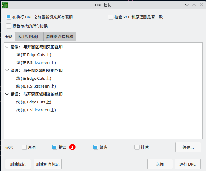
DRC 控制窗口的顶部部分包含一些控制设计规则检查器的选项:
Refill all zones before performing DRC: when enabled, zones will be refilled every time the design rule checker is run. Disabling this option may result in incorrect DRC results if zones have not been refilled manually.
Report all errors for each track: when enabled, all clearance errors will be reported for each track segment. When disabled, only the first error will be reported. Enabling this option will result in the design rule checker running more slowly.
Test for parity between PCB and schematic: when enabled, the design rule checker will test for differences between the schematic and PCB in addition to testing the PCB design rules. This option has no effect when running the PCB editor in standalone mode.
After running DRC, any violations will be shown in the center part of the DRC window. Rule violations, unconnected items, and differences between the schematic and the PCB are shown in three different tabs. A list of the ignored tests is shown in the fourth tab. A report file in plain text format can be created after running DRC using the Save… button.
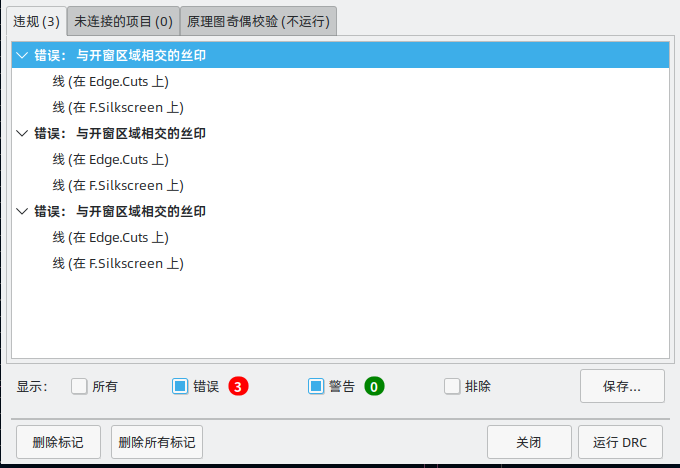
每个违规行为都涉及 PCB 上的一个或多个对象。 在违规列表中,涉及的对象列在违规行为下面。 点击列表中的违规行为将移动 “PCB 编辑器” 的视图,使受影响的区域居中。 点击违规所涉及的对象之一将高亮显示该对象。
Certain types of violations have contextual actions in the context menu. For example, clearance violations have an action to run the clearance resolution tool on the violating items, while custom rule violations have an action to run the constraint resolution tool. For board vs. library footprint mismatch violations, there is an action to run the Compare Footprint with Library tool. These actions can help to quickly identify the reason for a particular violation.
The numbers at the bottom of the window show the number of errors, warnings, and exclusions. Each type of violation can be filtered from the list using the respective checkboxes. Clicking Delete Marker will clear the selected violation until DRC is run again, while clicking Delete All Markers will clear all violations until the next DRC run.
可以在对话框中右键单击违规行为,以忽略它们或改变其严重程度:
-
Exclude this violation: ignores this particular violation, but does not affect any other violations. You can un-exclude a violation by right clicking the excluded violation and selecting Remove exclusion for this violation.
-
Exclude with comment…: the same as Exclude this violation, but prompts for a comment explaining the reason for the exclusion. When excluded violations are unhidden (using the Exclusions checkbox), exclusion comments are shown with the corresponding excluded violation. To edit an existing exclusion comment or add a comment to an existing exclusion, right click an excluded violation and select Edit exclusion comment….
-
Exclude all violations of rule: the same as Exclude this violation, but excludes all violations caused by the same custom DRC rule. This action only appears in the context menu for violations caused by custom design rules. If you right click on a custom design rule violation that is already excluded, you can instead Remove all exclusions for violations of rule.
-
Change severity: changes a type of violation from warning to error, or error to warning. This affects all violations of a given type.
-
Ignore all: ignores all violations of a given type. This test will now appear in the Ignored Tests tab rather than the Violations tab. You can un-ignore the test again by right clicking the test in the Ignored Tests tab, or in the Violation Severity panel in Board Setup.
-
Edit violation severities…: opens the Violation Severity panel in Board Setup, for editing the severities of all DRC violation types.
Excluded and ignored violations are remembered between runs of the design rule checker. Excluded violations are hidden unless the Exclusions checkbox is enabled. Ignored violations are not shown, but there is a list of ignored tests in the Ignored Tests tab.
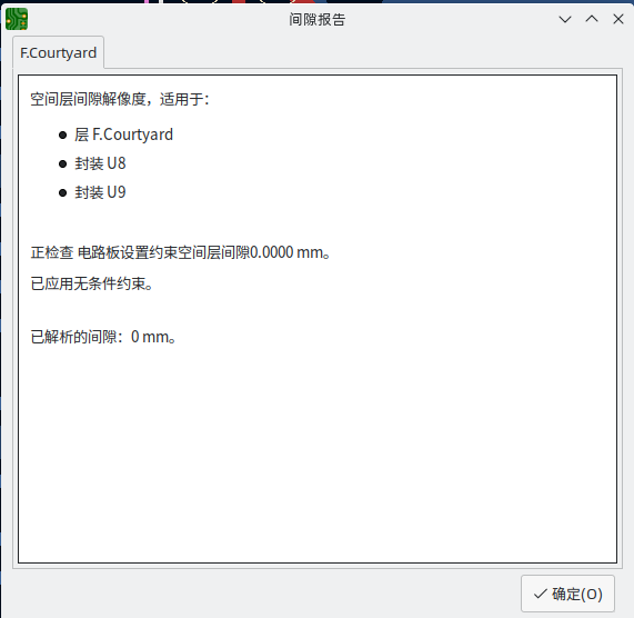
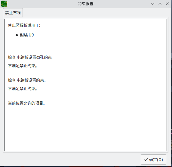
间隙和约束解析
间隙和约束解析工具允许你检查哪些间隙和设计约束规则应用于选定的项目。 当设计具有复杂设计规则的 PCB 时,这些工具可以提供帮助,因为在这种情况下并不总是清楚哪些规则适用于哪些对象。
要检查两个对象之间适用的间隙规则,选择这两个对象并从 检查 菜单中选择 间隙解析。 间隙报告对话框将显示每个铜层上的对象之间所需的间隙,以及产生该间隙的设计规则。
要检查适用于单一对象的设计约束,选择它并从 检查 菜单中选择 约束解析。 约束报告对话框将显示适用于该对象的所有约束。
DRC configuration
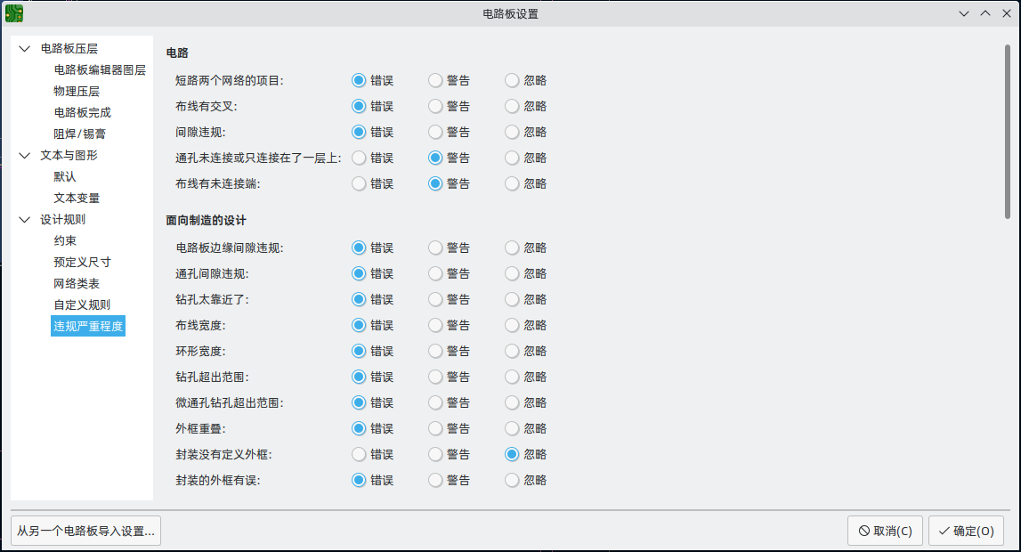
The severity of each DRC check can be configured in the Violation Severity section of the Board Setup dialog. Each rule may be set to create an error marker, a warning marker, or no marker (ignored).
| 在设计规则检查器中可能会忽略个别规则违规。 在违规程度部分中将规则设置为忽略将完全禁用相应的设计规则检查。 请谨慎使用此设置。 |
List of DRC checks
The table below lists the design rules that KiCad checks and the default violation severity for each check. All severities are configurable. Some design are only available through custom design rules.
Electrical DRC checks
These DRC checks look for gross electrical issues on the board such as shorts and clearance violations.
| Violation | Description | Default Severity |
|---|---|---|
Items shorting two nets |
This violation occurs when copper items on different nets collide with each other. If this is intentional, consider using a net tie. |
Error |
Tracks crossing |
This violation occurs when tracks with different nets cross each other. |
Error |
Clearance violation |
This violation occurs when the distance between two copper items with different nets is smaller than the configured clearance for those nets. The allowed clearance between two items can come from the board-level minimum clearance, the net class settings for each net, or from custom rules. To see detailed information about the configured and actual clearances between two selected items, run the clearance resolution tool, which is available by right clicking the violation in the DRC window. The minimum clearance path is highlighted in the editing canvas when a clearance violation is selected in the DRC window. This violation is also reported when the distance between two items is smaller than the configured physical clearance for those two items. Physical clearance constraints are not configured by default; see the custom rule documentation for how to configure physical clearance. |
Error |
Creepage violation |
This violation occurs when the creepage distance between two copper items with different nets is smaller than the configured creepage for those nets. Creepage paths are highlighted in the editing canvas when a creepage violation is selected in the DRC window. Creepage distances can be configured using a |
Error |
Via is not connected or is connected on only one layer |
This violation occurs when a via is connected to copper objects on only one layer or is not connected to anything. As vias are intended to connect copper objects on different layers, this may indicate that an intended connection is missing. |
Warning |
Track has unconnected end |
This violation occurs when the end of a track segment is not connected to another copper object, such as another track segment, a via or pad, or a zone or copper graphical shape. |
Warning |
Thermal relief connection to zone incomplete |
This violation occurs when a pad’s connection to a zone does not have enough connected thermal relief spokes. The minimum allowed number of spokes can come from the board-level minimum thermal relief spoke count or can be configured with more granularity using custom rules. This check counts automatically generated spokes as well as manually drawn connections, so if the pad and zone geometry prevent enough spokes from being generated, you can manually add additional connections using tracks between the pad and the zone. |
Error |
Design for manufacturing DRC checks
These DRC checks look for issues in the board that may cause manufacturing problems.
| Violation | Description | Default Severity |
|---|---|---|
Board edge clearance violation |
This violation occurs when the distance between a copper object and the
board edge is smaller than the configured copper to edge clearance for those
items. For the purposes of this check, oval holes (which are routed rather
than drilled) are counted as board edges in addition to any graphic items
on the The allowed edge clearance between two items can come from the board-level minimum copper to edge clearance or from custom rules. A negative edge clearance allows objects to overlap with the board edge. To see detailed information about the configured and actual edge clearances between two selected items, run the clearance resolution tool. |
Error |
Hole clearance violation |
This violation occurs when the distance between a hole (pad or via) and another copper object (pad, track, via, or zone) is smaller than the configured copper to hole clearance for those objects. Objects are only considered in this check if they have layers in common. The allowed hole clearance between two items can come from the board-level minimum copper to hole clearance or from custom rules. To see detailed information about the configured and actual hole clearances between two selected items, run the clearance resolution tool. This violation is also reported when the distance between a hole and another object is smaller than the configured physical hole clearance for those two items. Physical hole clearance constraints are not configured by default; see the custom rule documentation for how to configure physical hole clearance. |
Error |
Drilled hole too close to other hole |
This violation occurs when the distance between a drilled hole and another hole is smaller than the configured hole to hole clearance. Through vias, blind/buried vias, and through holes in pads are considered drilled holes because the holes are made with a physical drill bit, which can shift or be damaged if other holes (drilled or otherwise) are too close. Micro vias are not considered drilled holes because they are drilled using a laser, which is not affected by other nearby holes. At least one of the holes must be mechanically drilled in order to be considered in this check. Blind/buried vias are only considered in this check when they share layers with the other hole. Non-circular holes are not included in this check because they are routed rather than drilled. Routing is typically performed after holes are drilled and with a stronger tool. |
Error |
Drilled holes co-located |
This violation occurs when a drilled hole and another hole are in the exact same location. The same types of holes are considered in this check as for the "Drilled hole too close to other hole" check. |
Warning |
布线宽度 |
This violation occurs when the width of a track is outside of the configured range. The allowed width for a track can come from the board-level minimum track width or from custom rules. Note that an optimal track width can be configured for each net class in the net class settings, which sets a track width for the interactive router to use, but it does not set a minimum and maximum track width. No DRC violations will be reported for net class track width settings unless a minimum and/or maximum are configured using custom rules. To see detailed information about the configured track width for a particular track, run the constraints resolution tool. |
Error |
Track angle |
This violation occurs when the angle between two connected track segments is outside the configured range. Minimum and/or maximum allowable track angles can be configured using a
|
Error |
Track segment length |
This violation occurs when the length of a track segment is outside the configured range. Minimum and/or maximum allowable track segment lengths can be configured
using a |
Error |
Annular width |
This violation occurs when a pad or via’s annular width is outside of the configured range. Board-level minimum annular width can be configured in board setup constraints. Board-level maximum width, as well as more specific rules, can be configured using custom rules. |
Error |
Hole size out of range |
This violation occurs when a drilled hole’s diameter is outside of the configured range. This check represents the smallest hole that can be drilled, i.e. the smallest drill bit size the manufacturer will use. This check therefore includes through vias, blind/buried vias, and through holes in pads. Micro vias are not included in this check because they are made using a laser rather than a physical drill bit. Board-level minimum through hole size can be configured in board setup constraints. Board-level maximum hole size, as well as more specific rules, can be configured using custom rules. |
Error |
Micro via hole size out of range |
This violation occurs when a micro via’s hole diameter is outside of the configured range. This check represents the smallest hole that can be laser drilled and therefore only applies to micro vias. Board-level minimum micro via hole size can be configured in board setup constraints. Board-level maximum hole size, as well as more specific rules, can be configured using custom rules. |
Error |
Courtyards overlap |
This violation occurs when a footprint’s courtyard overlaps with another
footprint’s courtyard. A nonzero clearance between two courtyards can be
configured using a |
Error |
Footprint has no courtyard defined |
This violation occurs when a footprint does not contain any graphic
shapes on its |
Ignore |
Footprint has malformed courtyard |
This violation occurs when a footprint has a courtyard containing non-closed shapes. Courtyards may contain multiple unconnected shapes without being considered malformed, as long as each shape is individually closed. |
Error |
Board has malformed outline |
This violation occurs when the shapes on the |
Error |
Copper sliver |
This violation occurs when small, wedge-shaped protrusions of copper are detected. These slivers can cause manufacturing, reliability, or electrical issues. |
Warning |
Solder mask aperture bridges items with different nets |
This violation occurs when a single opening in the soldermask exposes multiple copper items with different nets. This can result in solder shorting the two copper items during assembly. |
Error |
Copper connection too narrow |
This violation occurs when a copper connection necks down to a width that is narrower than the configured minimum connection width. The minimum connection width setting can come from the board-level minimum connection width or can be configured with more granularity using custom rules. |
Warning |
Schematic parity DRC checks
These DRC checks look for differences between the schematic and the board.
| Violation | Description | Default Severity |
|---|---|---|
Duplicate footprints |
This violation occurs when the board contains multiple footprints with the same reference designator are in the board. It is not reported if the footprints do not correspond to schematic symbols, however (if the footprints only exist in the board). |
Warning |
Missing footprint |
This violation occurs when a footprint is not in the board but is expected based on a corresponding symbol in the schematic. |
Warning |
Extra footprint |
This violation occurs when a footprint is in the board without a corresponding symbol in the schematic. |
Warning |
Footprint attributes don’t match symbol |
This violation occurs when a footprint’s Typically this is fixed by performing an Update PCB from Schematic or Update Schematic from PCB action to sync the fields and attributes, depending on whether the symbol or footprint, respectively, is correct. |
Warning |
Footprint doesn’t match symbol’s footprint filters |
This violation occurs when a footprint does not match footprint filters in the corresponding symbol. If the symbol doesn’t have any footprint filters, no violation occurs. |
Ignore |
Pad net doesn’t match schematic |
This violation occurs when a net does not match between a footprint pad and the corresponding symbol pin. This can be because the symbol pin’s net is different than the footprint pad’s net, because the footprint pad does not have a corresponding symbol pin, or because the symbol pin does not have a corresponding footprint pad. |
Warning |
Missing connection between items |
This violation occurs when two copper objects with the same net are not connected on the board. |
Error |
Signal integrity DRC checks
These DRC checks look for signal integrity issues in the board.
| Violation | Description | Default Severity |
|---|---|---|
Track length out of range |
This violation occurs when a track in a differential pair is too long or too
short compared to the configured minimum and maximum length for that track.
The allowable track length for different tracks can be configured using the
|
Error |
Skew between tracks out of range |
This violation occurs when the difference between the length of a track and the maximum length of all tracks being considered is longer than the configured maximum skew for that set of tracks. For calculating the skew of a differential pair (two tracks), the skew therefore is calculated as the length difference between tracks. The allowable maximum skew for a set of tracks, as well as which tracks the
rule applies to, can be configured using the |
Error |
Too many or too few vias on a connection |
This violation occurs when the number of vias assigned to a net is too low
or too high compared to the configured minimum and maximum for that net. The
allowable via count for different nets can be configured using the
|
Error |
Differential pair gap out of range |
This violation occurs when the gap between the two tracks in a differential pair is too small or too large compared to the configured minimum and maximum for that differential pair. The gap is only checked on coupled (i.e. parallel) portions of the differential pair. The minimum and maximum allowable gap for a differential pair can be
configured using the Note that an optimal differential pair gap can be configured for each net class in the net class settings, which sets a gap for the differential pair router to use, but it does not set a minimum and maximum gap. No DRC violations will be reported unless a minimum and/or maximum are configured using custom rules. |
Error |
Differential uncoupled length too long |
This violation occurs when the portion of a differential pair that is uncoupled is longer than the configured maximum. A differential pair is considered uncoupled when its tracks are not parallel, for example when fanning out from a footprint. The maximum allowable uncoupled length for a differential pair can be
configured using the |
Error |
Readability DRC checks
These DRC checks look for issues that may affect legibility of text and other silkscreen objects on the board.
| Violation | Description | Default Severity |
|---|---|---|
Silkscreen overlap |
This violation occurs when a silkscreen object intersects another silkscreen object, which may affect readability. This check does not apply to silkscreen objects within the same footprint. The allowable distance between silkscreen objects can also be set to a nonzero number to enforce a silk to silk clearance using the board-level silkscreen minimum item clearance or using custom rules. A negative silkscreen clearance allows silkscreen to intersect other objects. |
Warning |
Silkscreen clipped by solder mask |
This violation occurs when a silkscreen object intersects a solder mask opening. This may result in silkscreen printed on bare copper or substrate. Board manufacturers may also discard any silkscreen that does not have solder mask underneath. Such outcomes could affect board assembly as well as silkscreen durability and readability. |
Warning |
Silkscreen clipped by board edge |
This violation occurs when a silkscreen object intersects a board edge, meaning that part of the silkscreen is outside of the board area. The allowable distance between silkscreen and the board edge can also be set to a nonzero number to enforce a clearance to the board edge using the board-level silkscreen minimum item clearance or using custom rules. A negative silkscreen clearance allows silkscreen to intersect other objects. |
Warning |
Text height out of range |
This violation occurs when a text object’s text height is outside of the configured range. Board-level minimum text height can be configured in board setup constraints. Board-level maximum height, as well as more specific rules, can be configured using custom rules. |
Warning |
Text thickness out of range |
This violation occurs when a text object’s text thickness is outside of the configured range. For the built-in KiCad stroke font, the thickness is the text thickness setting in the text object’s properties. For external fonts, this is the minimum physical thickness of all glyphs in the text object; this depends on the font geometry in combination with the font size, bold, and italic settings. Board-level minimum text thickness can be configured in board setup constraints. Board-level maximum thickness, as well as more specific rules, can be configured using custom rules. |
Warning |
Mirrored text on front layer |
This violation occurs when a text object on a front layer has the mirrored attribute set. When looking at the front of the board, the text will therefore appear backwards. |
Ignore |
Non-Mirrored text on back layer |
This violation occurs when a text object on a back layer doesn’t have the mirrored attribute set. When looking at the back of the board, the text will therefore appear backwards. |
Ignore |
Miscellaneous DRC checks
These DRC checks look for other miscellaneous issues in the board.
| Violation | Description | Default Severity |
|---|---|---|
Items not allowed |
This violation occurs when objects are placed in a location where they are
not allowed. This can be due to a rule area with a keep
out rule for the object’s type or due to a |
Error |
Copper zones intersect |
This violation occurs when copper zones with different nets collide with each other, shorting the two nets. |
Error |
Isolated copper fill |
This violation occurs when part of a copper fill is not connected to any other copper items with the same net. This is also referred to as an island. |
Warning |
Footprint is not valid |
This violation occurs when a footprint’s net tie group contains a pad that doesn’t exist in the footprint, or when a pad is in more than one net tie group. |
Error |
Padstack is questionable |
This violation occurs when a footprint pad has unusual settings that are probably a mistake. The settings that are checked are:
|
Warning |
PTH inside courtyard |
This violation occurs if a footprint’s plated through hole pad is within the courtyard of another footprint. Pads with the "heatsink pad" fabrication property are allowed, however. |
Warning |
NPTH inside courtyard |
This violation occurs if a footprint’s nonplated through hole pad is within the courtyard of another footprint. |
Warning |
Item on a disabled copper layer |
This violation occurs if an item, for example a pad or via, is on a copper layer that does not exist in the board stackup. |
Error |
Unresolved text variable |
This violation occurs when a text variable in the board design or drawing sheet does not resolve (there is no defined value for the variable). |
Error |
Footprint component type doesn’t match footprint pads |
This violation occurs when a footprint’s component type (SMD, through hole, or unspecified) doesn’t match the expected type based on the footprint’s pads. If a footprint contains any through hole pads, it is expected to have the through hole component type. If it contains SMD pads and no through hole pads, its component type is expected to be SMD. If a footprint’s component type is unspecified, the footprint is not compared against its pads. |
Ignore |
Footprint not found in libraries |
This violation occurs when a footprint in the board is not in an active library in the global library table or the project-specific library table. This can be because the footprint’s library does not contain the footprint, the footprint’s library is not listed in either library table, or because the library is listed in a table but is disabled. As a consequence, you will not be able to update the footprint from the library or compare changes between the board and library versions of the footprint. |
Warning |
Footprint doesn’t match copy in library |
This violation occurs when a footprint in the board is different than the library version of the footprint. You can compare between the board and library versions of the footprint using the Compare Footprint with Library tool, which is available by right clicking the violation in the DRC window. If desired, you can update the board footprint to match the library footprint. |
Warning |
Through hole pad has no hole |
This violation occurs when a through hole footprint pad does not have a hole. |
Error |
User-definable DRC violations
You can manually trigger board DRC warnings or errors using special text variables. These items will appear as errors or warnings when DRC runs. This can be useful to flag items for later followup or review.
To cause a DRC violation, use the text variable ${DRC_ERROR <violation name>} or ${DRC_WARNING <violation name>} depending on whether an error or warning is desired. You can place this in a text item or text box on any board layer. When DRC runs, this will generate a DRC violation with the given violation name. These text variables resolve to an empty string in the board, and any text after the braces is included in the DRC violation’s description. The text variable must be placed at the start of the text object in order to trigger a violation.
For example, a text item containing ${DRC_ERROR TODO}Length match tracks will appear in the board as just the text "Length match tracks", and will generate a DRC error named "TODO" with "Length matches tracks" in the description.
DRC report file
An DRC report file can be generated and saved by clicking the Save… button in the DRC dialog. The file extension for DRC report files is .rpt. An example DRC report file is given below.
** Drc report for pic_programmer.kicad_pcb **
** Created on 2024-11-02T15:54:52-0400 **

** Found 4 DRC violations **
[starved_thermal]: Thermal relief connection to zone incomplete (layer bottom_layer; 1 spokes connected to isolated island)
    Local override; error
    @(223.5200 mm, 138.4300 mm): Zone [GND] on bottom_layer
    @(175.2600 mm, 68.5800 mm): PTH pad 8 [GND] of P3
[starved_thermal]: Thermal relief connection to zone incomplete (layer bottom_layer; zone min spoke count 2; actual 1)
    Local override; error
    @(223.5200 mm, 138.4300 mm): Zone [GND] on bottom_layer
    @(207.8990 mm, 118.1100 mm): PTH pad 5 [GND] of U5
[starved_thermal]: Thermal relief connection to zone incomplete (layer bottom_layer; 1 spokes connected to isolated island)
    Local override; error
    @(223.5200 mm, 138.4300 mm): Zone [GND] on bottom_layer
    @(125.7300 mm, 111.7600 mm): PTH pad 10 [GND] of U2
[starved_thermal]: Thermal relief connection to zone incomplete (layer bottom_layer; zone min spoke count 2; actual 1)
    Local override; error
    @(223.5200 mm, 138.4300 mm): Zone [GND] on bottom_layer
    @(118.1100 mm, 111.7600 mm): PTH pad 13 [GND] of U2

** Found 0 unconnected pads **

** Found 0 Footprint errors **

** End of Report **
Board Statistics
The Board Statistics dialog shows a summary of the board’s contents, including the size of the board and counts of various types of items. Open the Board Statistics dialog with Inspect → Show Board Statistics.
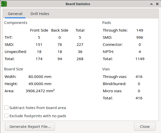
The General tab gives counts of various types of objects:
-
Footprints, separated by type (THT, SMD, or unspecified) and board side
-
Pads, separated by type (THT, SMD, connector, or NPTH)
-
Vias, separated by type (through, blind/buried, or micro)
It also displays the board width, height, and area.
The Drill Holes tab lists every unique type of drill hole on the board. Each type of hole is listed with its characteristics (shape, X and Y size, plating, pad or via type, and start and stop layers) and the count of that type of hole.
You can save the board statistics to a file by clicking the Generate Report File… button.
测量工具
测量工具允许你在 PCB 上的各点之间进行距离和角度测量。 要激活该工具,请点击右侧工具栏的 ![]() 图标,或使用快捷键 Ctrl+Shift+M。 一旦该工具被激活,点击一次以设置测量起点,然后再点击一次以完成测量。
图标,或使用快捷键 Ctrl+Shift+M。 一旦该工具被激活,点击一次以设置测量起点,然后再点击一次以完成测量。
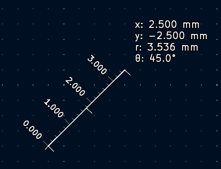
The tool displays the total (radial) distance between the points, the distance in X and Y directions, and the measured angle from horizontal. In other words, both the Cartesian and radial (polar) distances are displayed.
| 测量工具用于不需要永久显示的快速测量。 您所做的任何测量都将仅在该工具处于活动状态时显示。 要创建将显示在打印输出和打印中的永久性尺寸标注,请使用尺寸标注工具。 |
查找工具
查找工具在 PCB 中搜索文本,包括位号、封装字段和图形文本。当该工具找到一个匹配的文本时,画布会被放大,并将其置于匹配文本的中心位置,同时文本被高亮显示。使用顶部工具栏中的(![]() )按钮启动该工具。
)按钮启动该工具。
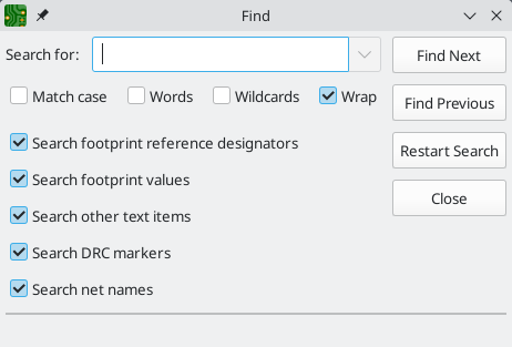
查找工具有几个选项:
Match case: Selects whether the search is case-sensitive.
Whole words only: When selected, the search will only match the search term with complete words in the PCB. When unselected, the search will match if the search term is part of a larger word in the PCB.
Wildcards: When selected, wildcards can be used in the search terms. ?
matches any single character, and * matches any number of characters. Note
that when this option is selected, partial matches are not returned: searching
for abc* will match the string abcd, but searching for abc will not.
Wrap: When selected, search results will return to the first hit after reaching the last hit.
Search footprint reference designators: Selects whether the search should apply to footprint reference designators.
Search footprint values: Selects whether the search should apply to footprint value fields.
Search other text items: Selects whether the search should apply to other text items, including graphical text and footprint fields other than value and reference.
Search DRC markers: Selects whether the search should apply to the violation descriptions of DRC markers shown on the board.
Search net names: Selects whether the search should apply to the names of nets in the board.
搜索面板
The search panel is a docked panel that lists information about footprints, zones, nets, ratsnest lines (unrouted segments), and text from the PCB. Show or hide the search panel with View → Panels → Search or use the Ctrl+G shortcut.
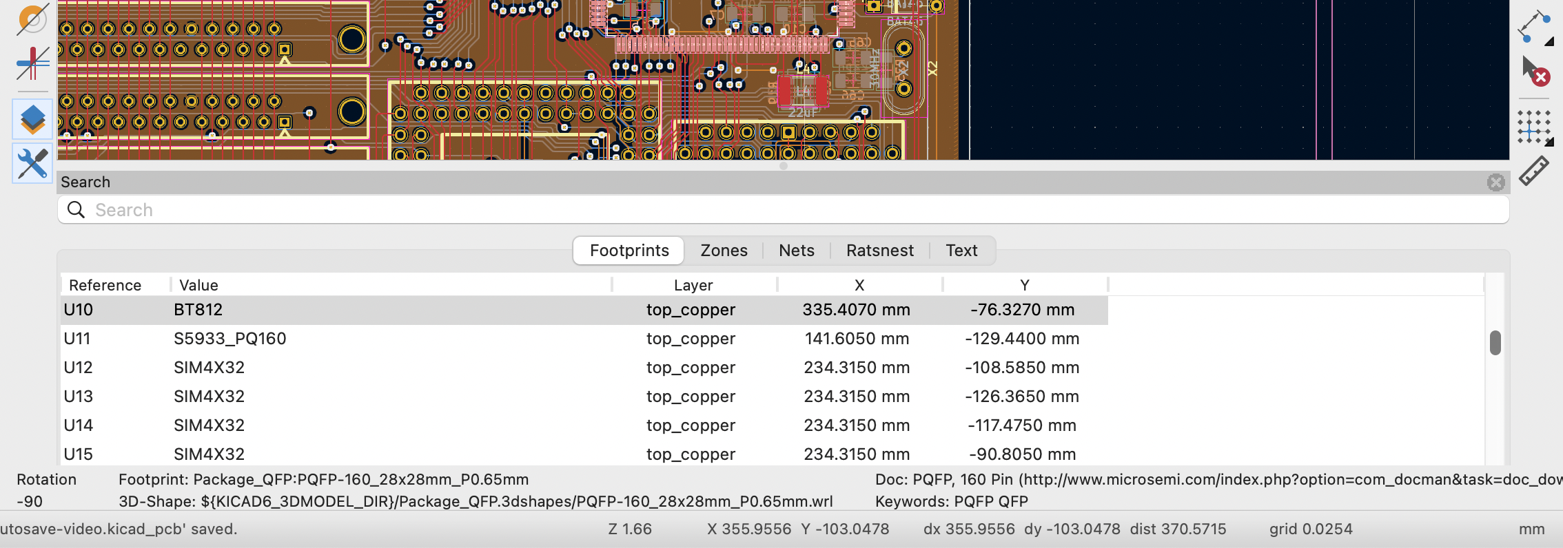
You can optionally filter the list based on a search string. When no filter is used, all items in the design are listed in the corresponding tab. Items are filtered based on their properties:
-
Footprints are filtered by the contents of their fields. You can select whether to search hidden fields by enabling the Search Hidden Fields option in the
 menu. Footprints are also filtered by their metadata (library link, description, and keywords) if Search Metadata is enabled in the menu.
 -
Zones are filtered by the zone name.
-
Net and ratsnest items are filtered by the net name.
-
Text (text, textboxes, and dimensions) is filtered by the text content.
You can sort the filtered results in ascending or descending order of the value in a particular column by clicking on that column header.
Filters support wildcards: * matches any characters, and ? matches any single character. You can also use regular expressions, such as /footprint value/.
The displayed information depends on the item type:
-
All items list their name and/or value.
-
Physical items (footprints, zones, and text) additionally list their layer and X/Y location.
-
Footprints additionally list their library link (library name and footprint name) and description.
-
Text additionally lists the type of text object (text, textbox, or dimension).
-
Net and ratsnest items additionally list their net name and net class.
When you click an item in the search panel, the item is selected in the editing canvas. Depending on what is configured in the ![]() menu, the board editor will also pan and/or zoom to the selected item in the editing canvas. Double-clicking an item in the search panel opens its properties dialog (for net and ratsnest items, the net classes dialog is opened instead).
menu, the board editor will also pan and/or zoom to the selected item in the editing canvas. Double-clicking an item in the search panel opens its properties dialog (for net and ratsnest items, the net classes dialog is opened instead).
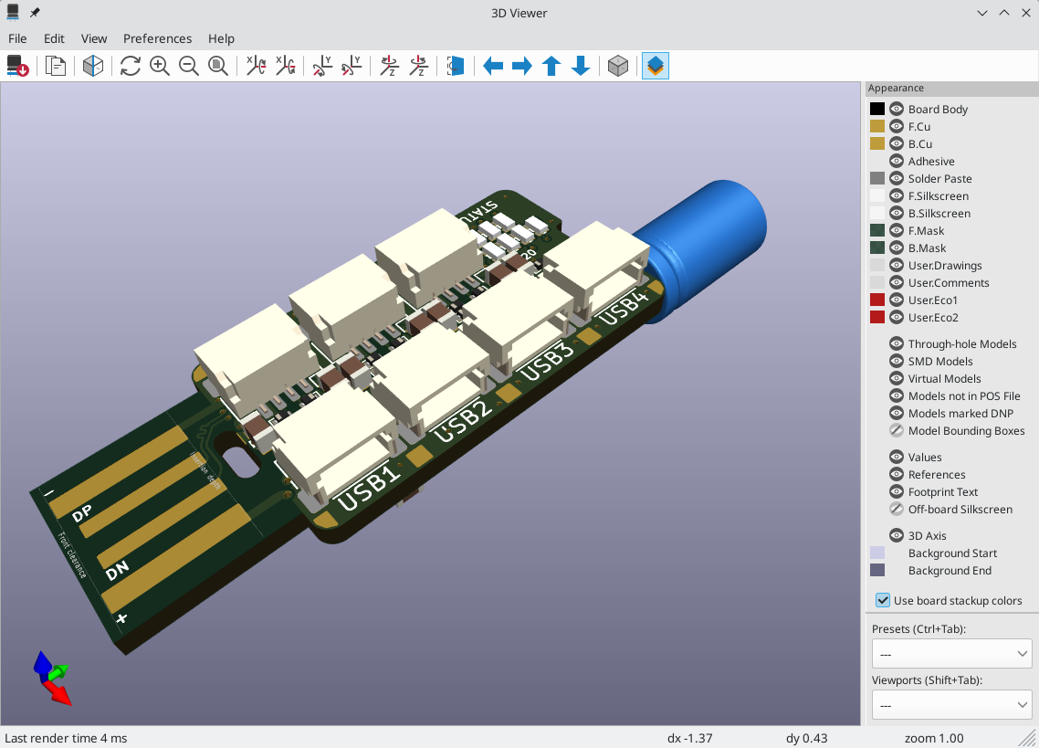
3D 查看器
The 3D Viewer shows a 3-dimensional view of the board and the components on the board. You can view the board from different perspectives, show or hide different types of components, cross-probe from the PCB Editor to the 3D viewer, and generate raytraced renders of the board. Show the 3D Viewer with View → 3D Viewer or use the Alt+3 shortcut.
| 仅当 3D 模型文件存在并且已被 分配到封装 时,元件的 3D 模型才会出现。 |
| KiCad 标准库中的许多封装还没有为它们创建模型文件。然而,这些封装可能包含一个指向尚不存在的 3D 模型的路径,以期待将来创建 3D 模型。 |
浏览 3D 视图
用鼠标左键拖动将旋转 3D 视图。 默认情况下,这是电路板的中心,但可以通过将光标移动到所需点上并按 Space 将轴心点重置为电路板上的新点。 滚动鼠标滚轮将放大或缩小视图。 按住 Ctrl 滚动可左右平移视图,按住 Shift 滚动可上下平移视图。 使用鼠标中键拖动也可以平移视图。
Different sized 3D grids can be set using the View → 3D Grid menu. Bounding boxes for each component can be enabled with Preferences → Show Model Bounding Boxes.
当 PCB 编辑器和 3D 查看器同时打开时,在 PCB 编辑器中选择一个封装也会在 3D 查看器中高亮显示该元件。高亮显示的颜色可以在 偏好设置 → 偏好设置… → 3D 查看器 → 实时渲染器 → 选择颜色 中调整。
Appearance Manager
The Appearance Manager is a panel at the right of the viewer which provides controls to manage the visibility, color, and opacity of different types of objects and board layers in the 3D view.
Each layer or type of object in the list can be individually shown or hidden by clicking its corresponding visibility icon. PCB layers can have their colors customized; double-click on the color swatch next to the item type to edit the item’s color and opacity. To use the colors selected in the Board Setup dialog’s Physical Stackup editor, enable the use board stackup colors option. If you enable the use PCB editor copper colors option, copper layers in the 3D viewer will use the colors configured in the PCB editor canvas.
You can save an appearance configuration as a preset, or load a configuration from a preset, using the Preset selector at the bottom. The Ctrl+Tab hotkey cycles through presets; press Tab repeatedly while holding Ctrl to cycle through multiple presets. Several built-in presets are available: "Follow PCB Editor" matches the visibility settings in the PCB editor, "Follow PCB Plot Settings" matches the visibility settings selected in the Plot dialog, and "legacy colors" matches the default 3D Viewer color settings from older versions of KiCad.
Finally, you can save a viewport for later retrieval using the Viewports selector at the bottom. You can quickly cycle between saved viewports using Shift+Tab; pressing Tab repeatedly while holding Shift will cycle through multiple viewports.
用 3D 查看器生成图像
当前的 3D 视图可以用 文件 → 将当前视图导出为 PNG… 或 将当前视图导出为 JPG…,根据所需的图像格式,将其保存为一个图像。也可以用 ![]() 按钮,或 编辑 → 复制 3D 图像 将当前视图复制到剪贴板上。
按钮,或 编辑 → 复制 3D 图像 将当前视图复制到剪贴板上。
3D 查看器有一个光线跟踪渲染模式,它使用比默认渲染模式更精确的物理渲染模型来显示电路板。 光线追踪比默认渲染模式慢,但当需要最吸引人的视觉效果时,可以使用它。使用 ![]() 按钮,或者使用 偏好设置→光线追踪 来启用光线追踪模式。在光线追踪模式下,3D 网格和选择高亮不会显示。
按钮,或者使用 偏好设置→光线追踪 来启用光线追踪模式。在光线追踪模式下,3D 网格和选择高亮不会显示。
颜色和其他渲染选项,包括光线跟踪和非光线跟踪模式,都可以在 偏好设置 → 偏好设置… → 3D查看器 中调整。
3D 查看器控制
许多查看选项是通过顶部的工具栏控制的。
|
Reload the 3D model |
|
Copy 3D image to clipboard |
|
Render current view using raytracing |
|
Redraw |
|
Zoom in |
|
Zoom out |
|
Fit drawing in display area |
|
Rotate X clockwise |
|
Rotate X counterclockwise |
|
Rotate Y clockwise |
|
Rotate Y counterclockwise |
|
Rotate Z clockwise |
|
Rotate Z counterclockwise |
|
Flip board view |
|
Pan board left |
|
Pan board right |
|
Pan board up |
|
Pan board down |
|
Enable/disable orthographic projection |
|
Show/hide the Appearance Manager |
网络检查
The Net Inspector is a docked panel that allows you to view statistics about all the nets in a board. It also lets you add, remove, and rename nets. To open the inspector, click the ![]() icon at the top of the Nets section of the Appearance panel, or select View → Panels → Net Inspector.
icon at the top of the Nets section of the Appearance panel, or select View → Panels → Net Inspector.
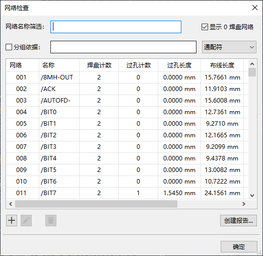
Double-clicking a net in the list will highlight that net on the board. You can also highlight a net by right clicking it and selecting Highlight Selected Net. If multiple nets are selected, this lets you highlight all of them at once. You can remove the net highlighting by right clicking the net’s row in the Net Inspector and selecting Clear Net Highlighting, in addition to the usual ways of removing net highlighting.
Clicking a column title allows you to sort the list of nets by that column. The Filter box lets you limit the listed nets to those that match the filter string. By default, the filter matches against both net names and net class names, but you can filter by just one or the other by selecting or deselecting Filter by Net Name or Filter by Netclass under the ![]() menu.
menu.
By default, nets with no connections and nets with no pads are not shown. You can choose to show them by selecting Show Unconnected Nets and Show Zero Pad Nets under the ![]() menu.
menu.
The Net Inspector shows the following statistics for each net:
-
Pad Count is the number of pads with that net, counting both surface mount and through hole pads.
-
Via Count is the number of vias with that net.
-
Via Length is the sum total length of all vias with that net. The full height of each via is always counted, even if the connections to the via are such that the full via height is not electrically used. In other words, Via Length is equal to Via Count multiplied by the stackup height of the board.
-
Track Length is the total length of all track segments in a net, not accounting for topology. For example, in a branching net structure all branches are included in the total length. The track length is also reported per copper layer.
-
Die Length is the total of all Pad to Die Length values set for pads on the net.
Each column can be shown or hidden in the ![]() → Show / Hide Columns menu. You can save the Net Inspector statistics to a CSV file by clicking
→ Show / Hide Columns menu. You can save the Net Inspector statistics to a CSV file by clicking ![]() → Save Net Inspector Report. The generated report includes all nets and columns, even if they are currently filtered or hidden in the Net Inspector.
→ Save Net Inspector Report. The generated report includes all nets and columns, even if they are currently filtered or hidden in the Net Inspector.
Grouping nets
You can group nets in the Net Inspector to organize them and view them more easily. Each group displays the total statistics for all its members, as if the group were a single net. For example, if you have a signal with a series resistor breaking the signal into two nets, you could create a group that contains both of these nets. This would allow you to analyze the total length of both nets, rather than each individually.
You can group nets by their net class by clicking ![]() → Group by netclass. Alternatively, you can create custom groups based on net name patterns. To create a new custom group, click
→ Group by netclass. Alternatively, you can create custom groups based on net name patterns. To create a new custom group, click ![]() → Add Custom Group. Any nets that contain the specified pattern in their name will be shown as part of the group and not shown outside of the group. For example, the pattern
→ Add Custom Group. Any nets that contain the specified pattern in their name will be shown as part of the group and not shown outside of the group. For example, the pattern CAN matches the nets CAN_RX and CAN_TX. Patterns are not case sensitive.
The pattern can also use regular expressions to match nets if the pattern is surrounded in slashes. For example, the pattern /^AN/ matches nets AN0, AN1, etc., but not CAN.
To remove a group and release its members back into the full list of nets, click ![]() → Remove Selected Custom Group. This action is also available in the right click menu. To remove all groups at once, click
→ Remove Selected Custom Group. This action is also available in the right click menu. To remove all groups at once, click ![]() → Remove All Custom Groups.
→ Remove All Custom Groups.
Editing nets
The Net Inspector allows you to create new nets in the board and remove or rename existing nets. To create a new net, right click in the Net Inspector and select Add Net, then provide a name for the new net. To delete a net, right click it in the list of nets and choose Delete Selected Net. If multiple nets are selected, they will all be deleted. To rename a net, right click it and choose Rename Selected Net, then provide a new name.
| Nets are usually not edited in the board. Instead, it is recommended to define nets in the schematic. Nets are typically managed in the board by creating or modifying a schematic and then using the Update PCB From Schematic tool to update the nets in the board based on the schematic design. The Net Inspector can be used to manage nets in alternate workflows that do not use a schematic. |
| Nets that are modified in the Board Editor will not effect the schematic until the schematic is updated from the PCB through the back-annotation process. |
Differences between Net Inspector and Length Tuner
The Net Inspector may report different net lengths than the length tuner, because the two tools have different purposes and calculate track/net lengths differently. In short, the Net Inspector sums up the total length of each track segment and via on a net, while the length tuner calculates the effective electrical length of a path between two points on a net. The specific differences are as follows:
-
The Net Inspector reports track length as a simple sum of the length of each track segment on a net. The length tuner calculates an effective electrical length of a net, which includes optimizing paths through pads to calculate the shortest possible path.
-
If a routed net has a branching topology, the Net Inspector total includes the length of each branch in the total. The length tuner calculates a point-to-point length; if there are any branches, the length tuner will stop at the closest branch and report the length up to the branch.
-
The Net Inspector always includes the effective via height in its via length and total length calculations. If a via connects to tracks on both the top and bottom layers, the full via height is included in the length calculation. Otherwise, only the stackup height between the connected layers is included. The length tuner calculates effective via height in the same way as the Net Inspector, but via height is only included in the length calculation when the use stackup height setting is enabled board constraint settings. If the setting is disabled, the length tuner will not include vias in its calculations at all.