KiCad Nightly Reference Manual
| This manual is in the process of being revised to cover the latest stable release version of KiCad. It contains some sections that have not yet been completed. We ask for your patience while our volunteer technical writers work on this task, and we welcome new contributors who would like to help make KiCad’s documentation better than ever. |
Copyright
This document is Copyright The KiCad Documentation Contributors. You may distribute it and/or modify it under the terms of either the GNU General Public License (http://www.gnu.org/licenses/gpl.html), version 3 or later, or the Creative Commons Attribution License (http://creativecommons.org/licenses/by/3.0/), version 3.0 or later.
Todas las marcas mencionadas en esta guía pertenecen a sus legítimos propietarios.
Contribuidores
Jean-Pierre Charras, Fabrizio Tappero, Wayne Stambaugh, Graham Keeth
Traducción
Antonio Morales <[email protected]>, 2015
Realimentación
The KiCad project welcomes feedback, bug reports, and suggestions related to the software or its documentation. For more information on how to submit feedback or report an issue, please see the instructions at https://www.kicad.org/help/report-an-issue/
Software and Documentation Version
This user manual is based on KiCad 10.99. Functionality and appearance may be different in other versions of KiCad.
Documentation revision: 2e473680.
Introduction to the KiCad Schematic Editor
The KiCad Schematic Editor is a schematic capture application distributed as a part of KiCad and available for the following operating systems:
-
Linux
-
Apple macOS
-
Windows
Regardless of the OS, all KiCad files are 100% compatible from one OS to another.
The Schematic Editor is an integrated application where all functions of schematic drawing, PCB footprint selection, library management, and data transfer to and from the PCB design software are carried out within the editor itself.
The KiCad Schematic Editor is intended to communicate directly with the KiCad PCB Editor for designing printed circuit boards without using any intermediate files. It can also export netlist files, which list all the electrical connections, for other packages.
The Schematic Editor includes a symbol library editor, which can create and edit symbols and manage libraries. It also integrates the following additional but essential functions needed for modern schematic capture software:
-
Electrical rules check (ERC) for automatic detection of incorrect and missing connections
-
Circuit simulation using ngspice
-
Exportación de ficheros de plano en múltiples formatos (Postscript, PDF, HPGL y SVG)
-
Bill of Materials generation (via Python or XSLT scripts, which allow many flexible formats).
The Schematic Editor supports multi-sheet schematics in several ways:
-
Flat hierarchies (schematic sheets are not explicitly connected in a master diagram).
-
Simple hierarchies (each schematic sheet is used only once).
-
Complex hierarchies (some schematic sheets are used multiple times).
Hierarchical schematics are described in detail later in the manual.
The Schematic Editor User Interface
The main Schematic Editor user interface is shown above, with some key elements indicated:
-
Top toolbars (file management, zoom tools, editing tools)
-
Message panel and status bar
-
Editing canvas
Navigating the editing canvas
The editing canvas displays the schematic being designed. You can pan and zoom to different parts of the schematic and open any schematic sheet in the design.
By default, dragging with the middle or right mouse button will pan the canvas view and scrolling the mouse wheel will zoom the view in or out. You can change this behavior in the Mouse and Touchpad section of the preferences (see Configuration and Customization for details).
Several other zoom tools are available in the top toolbar:
-
 zooms in on the center of the viewport.
 -
 zooms out from the center of the viewport.
 -
 zooms to fit the frame around the drawing sheet.
 -
 zooms to fit every item in the schematic (not including the drawing sheet). For instance, if there are items placed outside of the drawing sheet, they will be visible after zooming to objects.
 -
 allows you to draw a box to determine the zoomed area.
The cursor’s current position is displayed at the bottom of the window (X and Y), along with the current zoom factor (Z), the cursor’s relative position (dx, dy, and dist), the grid setting, and the display units.
The relative coordinates can be reset to zero by pressing Space. This is useful for measuring distance between two points or aligning objects.
Teclas rápidas
The Ctrl+F1 shortcut displays the current hotkey list. The default hotkey list is included in the Actions Reference section of the manual.
The hotkeys described in this manual use the key labels that appear on a standard PC keyboard. On an Apple keyboard layout, use the Cmd key in place of Ctrl, and the Option key in place of Alt.
Many actions do not have hotkeys assigned by default, but hotkeys can be assigned or redefined using the hotkey editor (Preferences → Preferences… → Hotkeys).
| Many of the actions available through hotkeys are also available in context menus. To access the context menu, right-click in the editing canvas. Different actions will be available depending on what is selected or what tool is active. |
Hotkeys are stored in the file user.hotkeys in KiCad’s configuration directory. The location is platform-specific:
-
Windows:
%APPDATA%\kicad\10.0\user.hotkeys -
Linux:
~/.config/kicad/10.0/user.hotkeys -
macOS:
~/Library/Preferences/kicad/10.0/user.hotkeys
KiCad can import hotkey settings from a user.hotkeys file using the Import Hotkeys button in the hotkey editor.
Selection and the selection filter
Selecting items in the editing canvas is done with the left mouse button. When no tool is active, single-clicking on an object will select it. Pressing Esc will always cancel the current tool or operation and return to the selection tool. Pressing Esc while the selection tool is active will clear the current selection.
You can also select items using a rectangle or lasso selection. These tools can be useful for selecting many items at once. You can switch between rectangular and lasso selection modes using the ![]() /
/ ![]() palette in the right toolbar.
palette in the right toolbar.
| To switch between multiple tools in a palette, show the palette by clicking and holding the left mouse button on the tool icon or by clicking and dragging the mouse from the tool icon. Release the mouse button on the desired tool to choose it. |
With the rectangular selection mode active (![]() ), clicking and dragging will perform a rectangular selection. A rectangular selection from left to right will only select items that are fully inside the box. A rectangular selection from right to left will select any items that touch the box. A left-to-right selection box is drawn in yellow, with a cursor that indicates exclusive selection, and a right-to-left selection box is drawn in blue with a cursor that indicates inclusive selection.
), clicking and dragging will perform a rectangular selection. A rectangular selection from left to right will only select items that are fully inside the box. A rectangular selection from right to left will select any items that touch the box. A left-to-right selection box is drawn in yellow, with a cursor that indicates exclusive selection, and a right-to-left selection box is drawn in blue with a cursor that indicates inclusive selection.
With the lasso selection mode active (![]() ), clicking and dragging will begin a lasso selection. Any items in the existing selection are deselected. Dragging with the left mouse button held draws a freeform shape. Releasing the button stops drawing the freeform shape and starts drawing a straight line. Clicking again completes the straight line. Any number of freeform or straight segments can be drawn by repeatedly clicking or dragging. Double click to finish drawing the lasso. Similar to a rectangular selection, a lasso drawn in a clockwise direction will only select items that are fully inside the lasso. A lasso drawn in a counter-clockwise direction will select any items that touch the lasso. A clockwise lasso is drawn in yellow, with a cursor that indicates exclusive selection, and a counter-clockwise lasso is drawn in blue with a cursor that indicates inclusive selection.
), clicking and dragging will begin a lasso selection. Any items in the existing selection are deselected. Dragging with the left mouse button held draws a freeform shape. Releasing the button stops drawing the freeform shape and starts drawing a straight line. Clicking again completes the straight line. Any number of freeform or straight segments can be drawn by repeatedly clicking or dragging. Double click to finish drawing the lasso. Similar to a rectangular selection, a lasso drawn in a clockwise direction will only select items that are fully inside the lasso. A lasso drawn in a counter-clockwise direction will select any items that touch the lasso. A clockwise lasso is drawn in yellow, with a cursor that indicates exclusive selection, and a counter-clockwise lasso is drawn in blue with a cursor that indicates inclusive selection.
The selection action can be modified by holding modifier keys while clicking or dragging. Modifiers cannot be used with lasso selections.
The following modifier keys apply when clicking to select single items:
| Modifier Keys (Windows) | Modifier Keys (Linux) | Modifier Keys (macOS) | Selection Effect |
|---|---|---|---|
Ctrl |
Ctrl |
Cmd |
Toggle selection. |
Shift |
Shift |
Shift |
Add the item to the existing selection. |
Ctrl+Shift |
Ctrl+Shift |
Cmd+Shift |
Remove the item from the existing selection. |
long click |
long click or Alt |
long click or Option |
Clarify selection from a pop-up menu. |
The following modifier keys apply when dragging to perform a rectangular selection:
| Modifier Keys (Windows) | Modifier Keys (Linux) | Modifier Keys (macOS) | Selection Effect |
|---|---|---|---|
Ctrl |
Ctrl |
Cmd |
Toggle selection. |
Shift |
Shift |
Shift |
Add item(s) to the existing selection. |
Ctrl+Shift |
Ctrl+Shift |
Cmd+Shift |
Remove item(s) from the existing selection. |
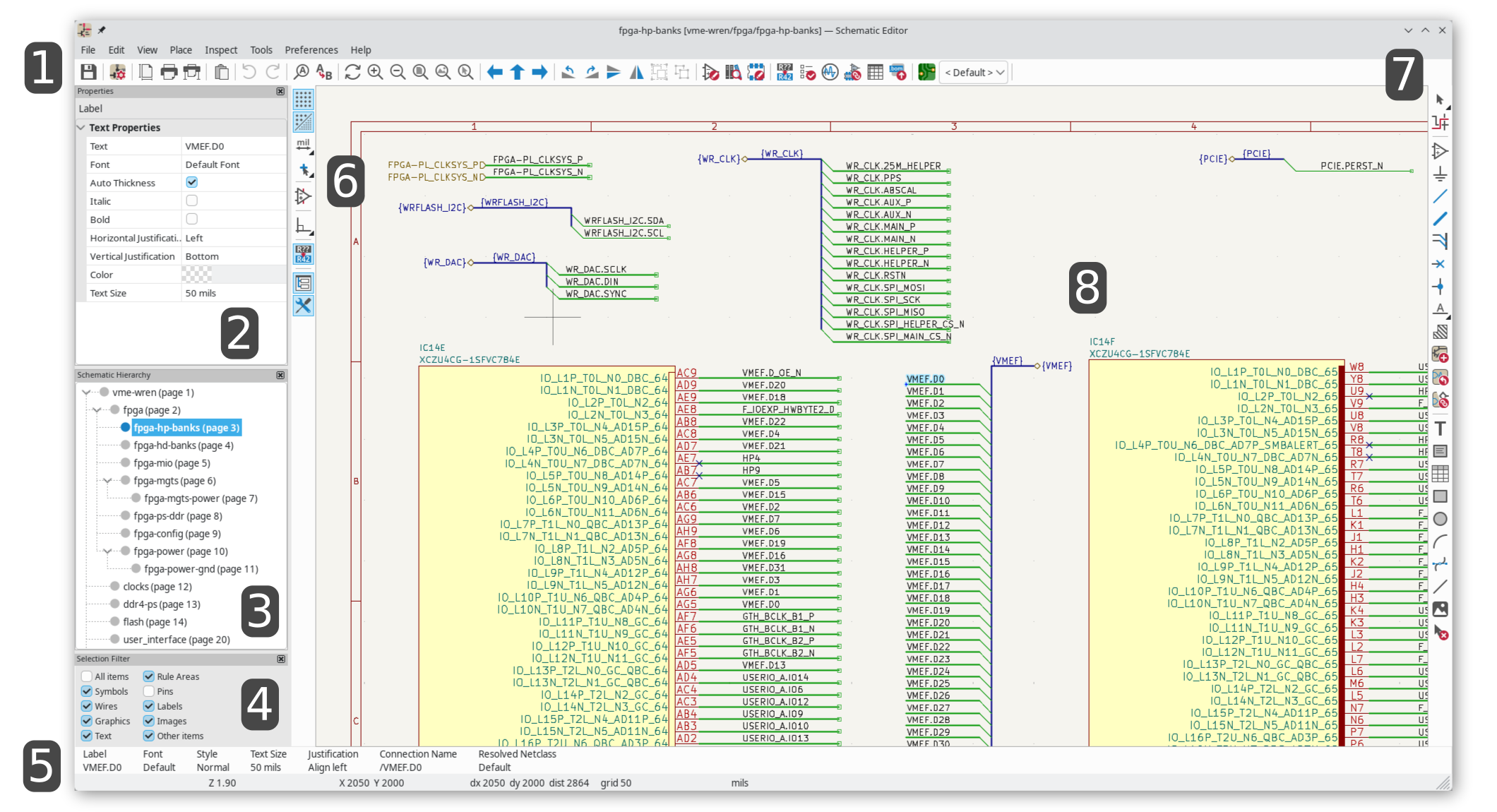
The selection filter panel in the lower left corner of the Schematic Editor window controls which types of objects can be selected with the mouse. Turning off selection of unwanted object types makes it easier to select items in a busy schematic.
The All items checkbox is a shortcut to turn the other items on and off. You can right-click any object type in the selection filter to quickly change the filter to only allow selecting that type of object.
If you repeatedly try to select an object whose type is disabled in the selection filter, the selection filter will visually flash the checkbox for that object type as a reminder that selecting that object type is disabled.
Selecting an object displays information about the object in the message panel at the bottom of the window. Double-clicking an object opens a window to edit the object’s properties.
Left toolbar display controls
The left toolbar provides options to change the display of items in the Schematic Editor.
Some toolbar buttons have more than one item available in a palette. These buttons are indicated with a small arrow in the lower-right corner of the button: 
To show the palette, you can click and hold the mouse button on the button or click and drag the mouse. The palette will show the selected item when it is closed.
The default contents of the left toolbar are shown below.
| You can edit the toolbar’s contents in the Toolbar page of the Schematic Editor Preferences. |
|
Turns grid display on/off. Note: by default, hiding the grid does not disable grid snapping. This behavior can be changed in the Display Options section of Preferences. |
|
Turns item-specific grid overrides on/off. |
|
Display/entry of coordinates and dimensions in inches, mils, or millimeters. Clicking the button toggles to the next unit, or you can choose a unit directly by expanding the palette (click and hold/drag). |
|
Switches the cursor crosshair between small, fullscreen, and 45-degree-rotated fullscreen. Clicking the button toggles to the next crosshair type, or you can choose a crosshair directly by expanding the palette (click and hold/drag). |
|
Turns invisible pin display on/off. |
|
Switches the line mode between free angle, 90 degree mode, and 45 degree mode for placement of new wires, buses, and graphical shapes. Clicking the button toggles to the next line mode, or you can choose a line mode directly by expanding the palette (click and hold/drag). You can also toggle between line modes using Shift+Space. |
|
Turns automatic symbol annotation on/off. When on, symbols will have their reference designators automatically set to the lowest available reference when they are added to the schematic. |
|
Opens and closes the docked Hierarchy Navigator panel. |
|
Opens and closes the docked Properties Manager panel. |
Creación y Edición de Esquemas
Introducción
A schematic designed with KiCad is more than a simple graphic representation of an electronic device. It is normally the entry point of a development chain that allows for:
-
Validar una serie de reglas (Comprobador de Reglas Eléctricas) para detectar errores y omisiones.
-
Automatically generating a bill of materials.
-
Generando netlist parar software de simulación como SPICE
-
Defining a circuit for transferring to PCB layout.
A schematic mainly consists of symbols, wires, labels, junctions, buses and power symbols. For clarity in the schematic, you can place purely graphical elements like bus entries, comments, and polylines.
Symbols are added to the schematic from symbol libraries. After the schematic is made, the set of connections and footprints is imported into the PCB editor for designing a board.
Schematics can be contained in a single sheet or split among multiple sheets. In KiCad, multi-sheet schematics are organized hierarchically, with a root sheet and sub-sheet(s). Each sheet is its own .kicad_sch file and is itself a complete KiCad schematic. Working with hierarchical schematics is described in the Hierarchical Schematics chapter.
Schematic editing operations
Schematic editing tools are located in the right toolbar. When a tool is activated, it stays active until a different tool is selected or the tool is canceled with the Esc key. The selection tool is always activated when any other tool is canceled.
Some toolbar buttons have more than one tool available in a palette. These tools are indicated with a small arrow in the lower-right corner of the button:
To show the palette, you can click and hold the mouse button on the button or click and drag the mouse. The palette will show the most recently selected item when it is closed.
The default contents of the right toolbar are shown below.
| You can edit the toolbar’s contents in the Toolbar page of the Schematic Editor Preferences. |
|
Selection tool (the default tool) When the rectangular selection mode is active, clicking and dragging performs a rectangular selection. When the lasso selection mode is active, clicking and dragging performs a lasso selection. Only one selection mode is visible in the toolbar at a time; you can expand the palette to choose another tool by clicking and holding/dragging. |
|
Highlight a net by marking its wires and net labels with a different color. If the PCB Editor is also open then copper corresponding to the selected net will be highlighted as well. Net highlighting can be cleared by clicking with the highlight tool in an empty space, or by using the Clear Net Highlighting hotkey (~). |
|
Display the symbol selector dialog to place a new symbol. |
|
Display the power symbol selector dialog to place a new power symbol. |
|
|
|
|
|
Draw wire-to-bus entry points. These elements are only graphical and do not create a connection, thus they should not be used to connect wires together. |
|
Place a "no-connection" flag. These flags should be placed on symbol pins which are meant to be left unconnected. "No-connection" flags indicate to the Electrical Rule Checker that the pin is intentionally unconnected and not an error. They also affect schematic connectivity for stacked symbol pins. |
|
Place a junction. This connects two crossing wires or a wire and a pin, which can sometimes be ambiguous without a junction (i.e. if a wire end or a pin is not directly connected to another wire end). |
|
Place a local label, directive label, global label, or hierarchical label. Local labels connect items located in the same sheet. Local labels with the same name are connected as long as they are in the same sheet. Global labels connect items located anywhere in the schematic. All global labels with the same name are connected, even when located on different sheets. Hierarchical labels are used to create a connection between a subsheet and the sheet’s parent sheet. See the Hierarchical Schematics section for more information about hierarchical labels, sheets, and pins. Directive labels are used to assign net classes to individual nets. They can also be used to assign net classes and component classes to nets and symbols, respectively, inside rule areas. Only one label type is visible in the toolbar at a time; you can expand the palette to choose another tool by clicking and holding/dragging. |
|
Place a rule area. |
|
Place a hierarchical subsheet. You must specify the file name for this subsheet. |
|
Place a hierarchical sheet pin on a sheet corresponding to a hierarchical label that has been added in the target sheet. |
|
Sync hierarchical sheet pins and hierarchical labels. This displays a list of all the hierarchical labels in each subsheet and lets you manage the corresponding hierarchical sheet pins. |
|
|
|
|
|
|
|
|
|
|
|
|
|
|
|
Note: Lines are graphical objects and are not the same as wires placed with the Wire tool. They do not connect anything. |
|
|
|
Delete clicked items. |
Grids and snapping
Schematic elements such as symbols, wires, text, and graphic lines are snapped to the grid when moving, dragging, and drawing them. Additionally, the wire and label tools snap to other connected items such as pins, wires, and labels even when grid snapping is disabled.
Both grid and connected object snapping can be disabled while moving the mouse by using the modifier keys in the table below.
| On Apple keyboards, use the Cmd key instead of Ctrl. |
| Modifier Key | Effect |
|---|---|
Ctrl |
Disable grid snapping. |
Shift |
Disable connected object snapping. |
The default grid size is 50 mil (0.050") or 1.27 millimeters. This is the recommended grid for placing symbols and wires in a schematic and for placing pins when designing a symbol in the Symbol Editor. Smaller grids can also be used, but this is intended only for text and symbol graphics, and not recommended for placing pins and wires.
| Wires connect with other wires or pins only if their ends coincide exactly. Therefore it is very important to keep symbol pins and wires aligned to the grid. It is recommended to always use a 50 mil grid when placing symbols and drawing wires because the KiCad standard symbol library and all libraries that follow its style also use a 50 mil grid. Using a grid size other than 50 mil will result in schematics without proper connectivity! |
| Symbols, wires, and other elements that are not aligned to the grid can be snapped back to the grid by selecting them, right clicking, and clicking Align Elements to Grid. |
You can adjust the grid size by right-clicking and selecting a new grid from the list in the Grid submenu. Pressing the n or N hotkeys will cycle to the next and previous grid in the list, respectively.
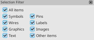
You can also select a new grid or edit the available grids in the Grids pane of the preferences dialog. As a shortcut to reach this dialog, right click the ![]() button on the left toolbar and select Edit Grids….
button on the left toolbar and select Edit Grids….
In this dialog you can select an active grid from the list of grids, reorder the list of grids (![]() /
/ ![]() ), and add (
), and add (![]() ), remove (
), remove (![]() ), or edit (
), or edit (![]() ) grids. Grids defined in this dialog can have unequal X and Y spacing as well as an optional name. The grid spacing and name are specified when you create or edit a grid.
) grids. Grids defined in this dialog can have unequal X and Y spacing as well as an optional name. The grid spacing and name are specified when you create or edit a grid.
This dialog also lets you designate two grids from the list as "Fast Grids", which can be quickly selected using Alt+1 and Alt+2.
Finally, you can configure grid overrides for different types of objects. Grid overrides let you set particular grid sizes for different types of objects which will be used instead of the default grid when working with those objects. For example, you can set a 50 mil grid for wires and connected items while using smaller grids to finely position text and graphics. Grid overrides can be individually enabled and disabled in this dialog, or globally enabled and disabled using the ![]() button on the left toolbar (Ctrl+Shift+G).
button on the left toolbar (Ctrl+Shift+G).
The visual appearance of the grid can also be customized in several ways. You can change the thickness of the grid markings, switch their shape (dots, lines, or crosses), and set the minimum displayed spacing in the Display Options page of the preferences dialog, and you can change the grid color in the Colors page of the preferences dialog.
The grid can be shown or hidden using the ![]() button on the left-hand toolbar. By default the grid is still active even if it is hidden, but this is configurable in the Display Options preferences page. There you can set the grid to be disabled when it is hidden or even disable the grid entirely.
button on the left-hand toolbar. By default the grid is still active even if it is hidden, but this is configurable in the Display Options preferences page. There you can set the grid to be disabled when it is hidden or even disable the grid entirely.
Editing object properties
All objects have properties that are editable in a dialog. Use the hotkey E or select Properties from the right-click context menu to edit the properties of selected item(s). You can only open the properties dialog if all the items you have selected are of the same type. For many object types, like symbols, you can only edit the properties of a single item at one time. To edit the properties of multiple items at once, including items with different types, you can use the Properties Manager.
You can only use the properties dialog to edit one item at a time. To edit multiple items, use the Properties Manager, described below. There are also other tools that can be used to edit specific types of objects in bulk, such as the Edit Text and Graphics tool for editing visual properties of text, symbol fields, labels, and graphic shapes, or the Symbol Fields Table for editing symbol fields in bulk.
You can also view and edit item properties using the Properties Manager. The Properties Manager is a docked panel that displays the properties of the selected item or items for editing. If multiple types of items are selected at once, the properties panel displays only the properties shared by all of the selected item types.
Editing a property in the Properties Manager immediately applies the change. When multiple items are selected, property modifications are applied to each selected item individually, not to the whole selection as a group. For example, when changing the orientation of multiple items, each item is individually rotated around its own origin, not the group’s origin.
Show the Properties Manager with View → Panels → Properties or the ![]() button on the left toolbar.
button on the left toolbar.
In properties dialogs and many other dialogs, any field that contains a numeric value can also accept a basic math expression that results in a numeric value.
For example, a dimension may be entered as 2 * 2mm, resulting in a value of 4mm. Basic arithmetic operators as well as parentheses for defining order of operations are supported. Units can also be specified, and unit conversions are performed automatically, so 1in + 1mm evaluates to 26.4mm.
Working with symbols
Placing symbols
To place a symbol in your schematic, use the ![]() button or the A hotkey. The Choose Symbols dialog appears and lets you select a symbol to add. Symbols are grouped by symbol library.
button or the A hotkey. The Choose Symbols dialog appears and lets you select a symbol to add. Symbols are grouped by symbol library.
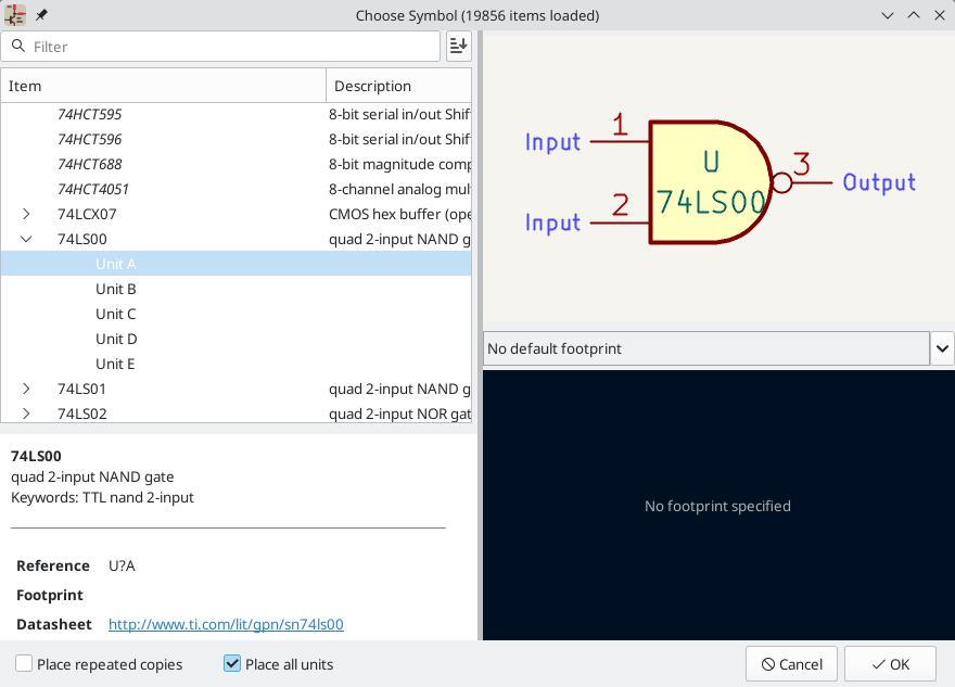
By default, only the symbol/library name and description columns are shown. Additional columns can be added by right-clicking the column header and selecting Select Columns.
The Choose Symbol dialog filters symbols by name, keywords, description, and all additional symbol fields according to what you type into the search field. You can choose to sort search results alphabetically or by best match by clicking on the ![]() button.
button.
Some advanced filters are available:
-
Wildcards:
*matches any number of any characters, including none, and?matches any single character. -
Key-value pairs: if a library part’s description or keywords contain a tag of the format "Key:123", you can match relative to that by typing "Key>123" (greater than), "Key<123" (less than), etc. Numbers may include one of the following case-insensitive suffixes:
p
n
u
m
k
meg
g
t
10-12
10-9
10-6
10-3
103
106
109
1012
ki
mi
gi
ti
210
220
230
240
-
Regular expressions: if you’re familiar with regular expressions, these can be used too. The regular expression flavor used is the wxWidgets Advanced Regular Expression style, which is similar to Perl regular expressions.
If the symbol specifies a default footprint, this footprint will be previewed in the lower right. If the symbol includes footprint filters, alternate footprints that satisfy the footprint filters can be selected in the footprint dropdown menu at right.
After selecting a symbol to place, the symbol will be attached to the cursor. Left clicking the desired location in the schematic places the symbol into the schematic. Before placing the symbol in the schematic, you can rotate it, mirror it, and edit its fields, by either using the hotkeys or the right-click context menu. These actions can also be performed after placement.
If the Place repeated copies option is checked, after placing a symbol KiCad will start placing another copy of the symbol. This process continues until the user presses Esc.
For symbols with multiple units, if the Place all units option is checked, after placing the symbol KiCad will start placing the next unit in the symbol. This continues until the last unit has been placed or the user presses Esc.
Placing power symbols
A power symbol is a symbol representing a connection to a power net. The symbols are grouped in the power library, so they can be placed using the symbol chooser. However, as power placements are frequent, the ![]() tool is available. This tool is similar, except that the search is done directly in the
tool is available. This tool is similar, except that the search is done directly in the power library and any other library that contains power symbols.
Moving symbols
Symbols can be moved using the Move (M) or Drag (G) tools. These tools act on the selected symbol, or if no symbol is selected they act on the symbol under the cursor.
The Move tool moves the symbol itself without maintaining wired connections to the symbol pins.
The Drag tool moves the symbol without breaking wired connections to its pins, and therefore moves the connected wires as well.
You can also Drag symbols by clicking and dragging them with the mouse, depending on the Left button drag gesture setting in the Mouse and Touchpad section of Preferences.
Symbols can also be rotated (R) or mirrored in the X (X) or Y (Y) directions.
Editing symbol properties
Symbols in the schematic can be individually edited, both in terms of their properties (fields, attributes, etc.) and in terms of their pins and graphics. Editing a symbol in the schematic only affects that particular instance of the symbol; it does not affect any other copies of that symbol in the schematic, and it does not affect the library symbol.
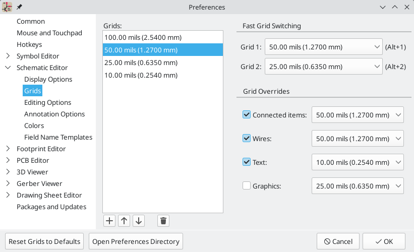
To edit the properties of a symbol in the schematic, open its properties dialog (E). You can also double-click the symbol.
The majority of the settings in this dialog are the same as in the symbol editor. You can edit the symbol’s fields, attributes, pin functions, and embedded files, as in the symbol editor.
The Symbol Properties window displays all the fields of a symbol in a table. New fields can be added, and existing fields can be deleted, edited, reordered, moved, or resized. Fields can be arbitrarily named, but names beginning with ki_, e.g. ki_description, are reserved by KiCad and should not be used for user fields. All symbol fields will be added to the symbol’s corresponding footprint when the PCB is updated from the schematic.
Each field’s name and value can be visible or hidden, and there are several formatting options: horizontal and vertical alignment, orientation, position, font, text color, text size, and bold/italic emphasis. Field autoplacement can also be enabled on a per-field basis. The displayed position is always indicated for a normally displayed symbol (no rotation or mirroring) and is relative to the anchor point of the symbol.
| Formatting options for symbol fields can be shown or hidden by right-clicking on the header row of the symbol field table and enabling or disabling the desired columns. Not all columns are shown by default. |
Several fields have special behavior:
-
The Footprint field defines which footprint will correspond to the symbol in the board design. When the footprint field is selected, you can click the
 button to open the footprint chooser to assign a footprint to the symbol. See the Assigning Footprints section for other ways to assign footprints.
 -
The Datasheet field can contain the manufacturer’s datasheet for the symbol. You can right click a symbol in the editing canvas and choose Show Datasheet (D) to open the datasheet listed in the symbol. A symbol’s datasheet can be a local file or a file at a remote URL, like the manufacturer’s website. You can choose a local file using a file browser by selecting the datasheet field in the symbol’s properties, then clicking the
 button. If you enable the Embed File checkbox in the file browser, the datasheet will be embedded in the schematic instead of being referenced as an an external file. This means the datasheet will be available on any computer. For more information, see the embedded files documentation.
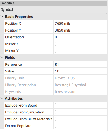
Symbols have several attributes that affect how the symbols are treated by other parts of KiCad.
-
Exclude from simulation prevents the symbol from being included in SPICE simulations. Symbols that are excluded from simulation are drawn with a grey outline around them and a simulation waveform icon to their bottom right, as shown below. The color of the outline and icon is configurable by editing the "Excluded-from-simulation Markers" color in the selected colorscheme. The visual marker (the outline and the icon) can be disabled completely by disabling View → Mark items which are excluded from simulation.

-
Exclude from bill of materials prevents the component from being included in BOM exports.
-
Exclude from board means that the symbol is schematic-only, and a corresponding footprint will not be added to the PCB.
-
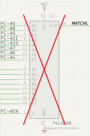
Do not populate means that the component should not be attached to the PCB, although a corresponding footprint should still be added to the board. DNP symbols appear desaturated and with a red "X" over them in the schematic, as shown below. The color of the "X" is configurable by editing the "DNP Markers" color in the selected colorscheme.
To edit the symbols’s form, i.e. its pins and graphics, you need to use the symbol editor. There are two buttons for opening a symbol in the editor, depending on whether you want to edit a single copy of a symbol in the schematic or a symbol’s source copy in the library.
-
Edit Symbol… will open the specific instance of the symbol in the symbol editor. Editing this symbol will only affect this one instance of the symbol in the schematic. It will not affect other instances of the symbol in the schematic, and it will not affect the library copy of the symbol. You can also open a schematic symbol in the symbol editor by right clicking the symbol in the schematic and selecting Edit with symbol editor (Ctrl+E).
-
Edit Library Symbol… will open the library copy of the symbol in the symbol editor. Editing the library copy of the symbol will edit the symbol in the symbol library, but will not immediately affect any instances of that symbol in the schematic. To update symbols in the schematic with changes to the library symbol, use the Update Symbol from Library… tool. Editing the library symbol in this way is equivalent to opening the symbol editor, opening the appropriate symbol in its library, and editing it.
The Update Symbol from Library… button is used to update the schematic’s copy of the symbol to match the copy in the library. The Change Symbol… button is used to swap the current symbol to a different symbol in the library. These functions are described later.
The Simulation Model… button opens the Simulation Model Editor for specifying the symbol’s behavior in SPICE simulations.
Editing symbol fields individually
An individual symbol text field can be edited directly with the E hotkey (with a field selected instead of a symbol) or by double-clicking on the field.
Some symbol fields have their own hotkey to edit them directly. With the symbol selected, the Reference, Value, and Footprint fields can be edited with the U, V, or F hotkeys, respectively.
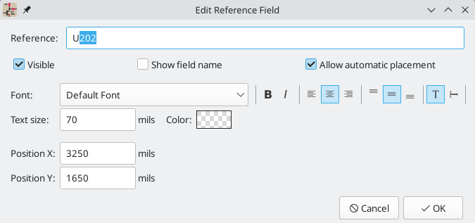
The options in this dialog are the same as those in the full Symbol Properties dialog, but are specific to a single field.
Symbol fields can be automatically moved to an appropriate location with the Autoplace Fields action (select a symbol and press O). Field autoplacement is configurable in the Schematic Editor’s Editing Options, including a setting to always autoplace fields. You can also disable autoplacement for individual fields in the Symbol Properties or Field Properties dialogs.
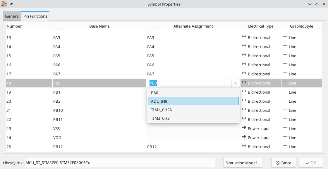
Alternate pin functions
Symbol pins can have alternate pin functions defined for them. Alternate pin functions allow you to select a different name, electrical type, and graphical style for a pin when a symbol has been placed in the schematic. This can be used for pins that have multiple functions, such as microcontroller pins.
Alternate pin functions are selected once a symbol has been placed in the schematic. The pin function is selected in the Pin Functions tab of the Symbol Properties dialog. Alternate definitions are selectable in the dropdown in the Alternate Assignment column. You can also select an alternate pin by right-clicking the pin and selecting a new function from the Pin Function menu.
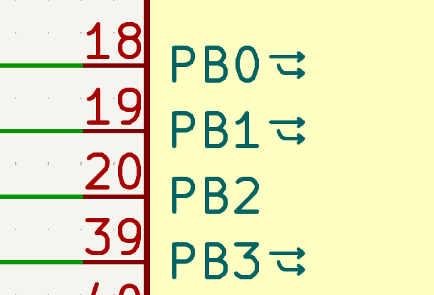
Pins that have alternate functions available are displayed with a small graphical indicator next to the pin name, as shown in the screenshot below. To globally show or hide these indicators, use View → Show Pin Alternate Icons.
For information on how to add alternate pin functions to symbols, see the symbol editor documentation.
Updating and exchanging symbols
When a symbol is added to the schematic, KiCad embeds a copy of the library symbol in the schematic so that the schematic is independent of the system libraries. Symbols that have been added to the schematic are not automatically updated when the library changes. Library symbol changes are manually synced to the schematic so that the schematic does not change unexpectedly.
| You can use the Compare Symbol with Library tool to inspect the differences between a symbol in a schematic with its corresponding library symbol. |
To update symbols in the schematic to match the corresponding library symbol, use Tools → Update Symbols from Library…, or right click a symbol and select Update Symbol…. You can also access the tool from the symbol properties dialog.
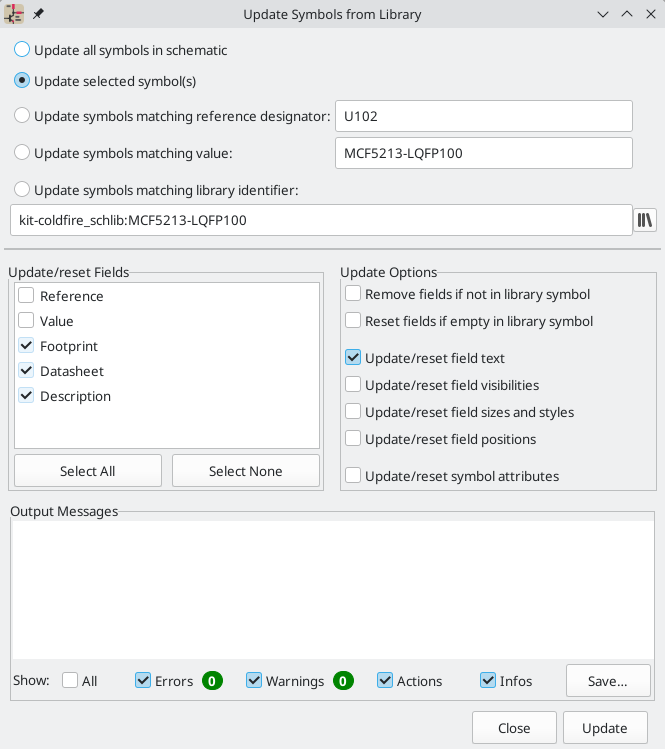
The top of the dialog has options to choose which symbols will be updated:
-
Update all symbols in schematic: all symbols in the schematic will be updated to match the library versions of the symbols.
-
Update selected symbol(s): symbols that are selected in the schematic will be updated.
-
Update symbols matching reference designator: symbols matching the specified reference designator will be updated. The reference designator field supports wildcards:
*matches any number of any characters, including none, and?matches any single character. -
Update symbols matching value: symbols with the specified value will be updated. The value field supports wildcards:
*matches any number of any characters, including none, and?matches any single character. -
Update symbols matching library identifier: symbols that match the specified library identifier will be updated. Library identifiers consist of the symbol library name and the symbol name, separated by
:.
The middle of the dialog has options to control what parts of the symbol will be updated. On the left, you can select which fields will be modified (updated or reset). On the right, you can select how to update those fields:
-
Remove fields if not in library symbol: if selected, any fields that are in the schematic version of the symbol but not the library version will be deleted.
-
Reset fields if empty in library symbol: if selected, any fields that are empty in the library version of the symbol will be set to empty in the schematic version of the symbol.
-
Update/reset field text: if selected, field contents in the schematic version of the symbol will be updated to match the fields in the library version of the symbol. Any fields that are empty in the library version of the symbol will not be updated unless Reset fields if empty in library symbol is selected.
-
Update/reset field visibilities: if selected, fields in the schematic version of the symbol will have their visibility updated to match the library version of the symbol.
-
Update/reset field text sizes and styles: if selected, fields in the schematic version of the symbol will have their text sizes and styles updated to match the library version of the symbol.
-
Update/reset field positions: if selected, fields in the schematic version of the symbol will be moved to match the locations of the fields in the library version of the symbol.
-
Update symbol shape and pins: the symbol’s shape and pins are always updated to match the library version of the symbol.
-
Update keywords and footprint filters: The symbol’s keywords and footprint filters are always updated to match the library version of the symbol.
-
Update/reset pin name/number visibilities: if selected, the visibility of pin names and numbers in the schematic version of the symbol will be updated to match the visibility of the pin names and numbers in the library version of the symbol.
-
Reset alternate pin functions: if selected, alternate pin functions selected for the symbol’s pins will be reset to default pin functions.
-
Update/reset symbol attributes: if selected, the schematic symbol attributes (do not populate, exclude from simulation, exclude from BOM, exclude from board) will be updated to match the library version of the symbol.
-
Reset custom power symbols: if selected, the
Valuefield of power symbols in the schematic will be updated to match the library versions of the symbols. If not selected, theValuefield of power symbols will not be updated, even if theValuefield of other non-power symbols would be updated. Note that changing theValuefield of power symbols will change the global net associated with the power symbol.
The bottom of the dialog displays messages describing the update actions that have been performed, with filters for which types of messages to display (errors, warnings, actions, and/or infos).
To change an existing symbol to a different symbol, use Edit → Change Symbols…, or right click an existing symbol and select Change Symbol…. This dialog is also accessible from the symbol properties dialog.
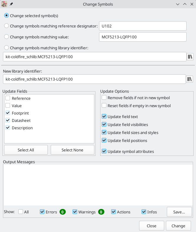
The options for the Change Symbols dialog are very similar to the Update Symbols from Library dialog.
Another way to swap existing symbols for new ones is to use Tools → Edit Symbol Library Links…. This dialog contains a table of every symbol in the design, grouped by current library symbol. By choosing a new symbol in the New Library Reference column, you can make all instances of the existing symbol instead point to the new symbol. If the Update symbol fields from new library option is used, the contents of the existing symbols' fields will be updated to match the new symbols' fields.
The Map Orphans button attempts to automatically remap orphaned symbols to symbols with the same name in an active library. For example, if there is a symbol with the current library reference mylib:symbol123, but the mylib library cannot be found, the Map Orphans button will attempt to find a symbol named symbol123 in any of the libraries that are present. This button is only enabled if orphaned symbols are present in the schematic (see the legacy schematics section).
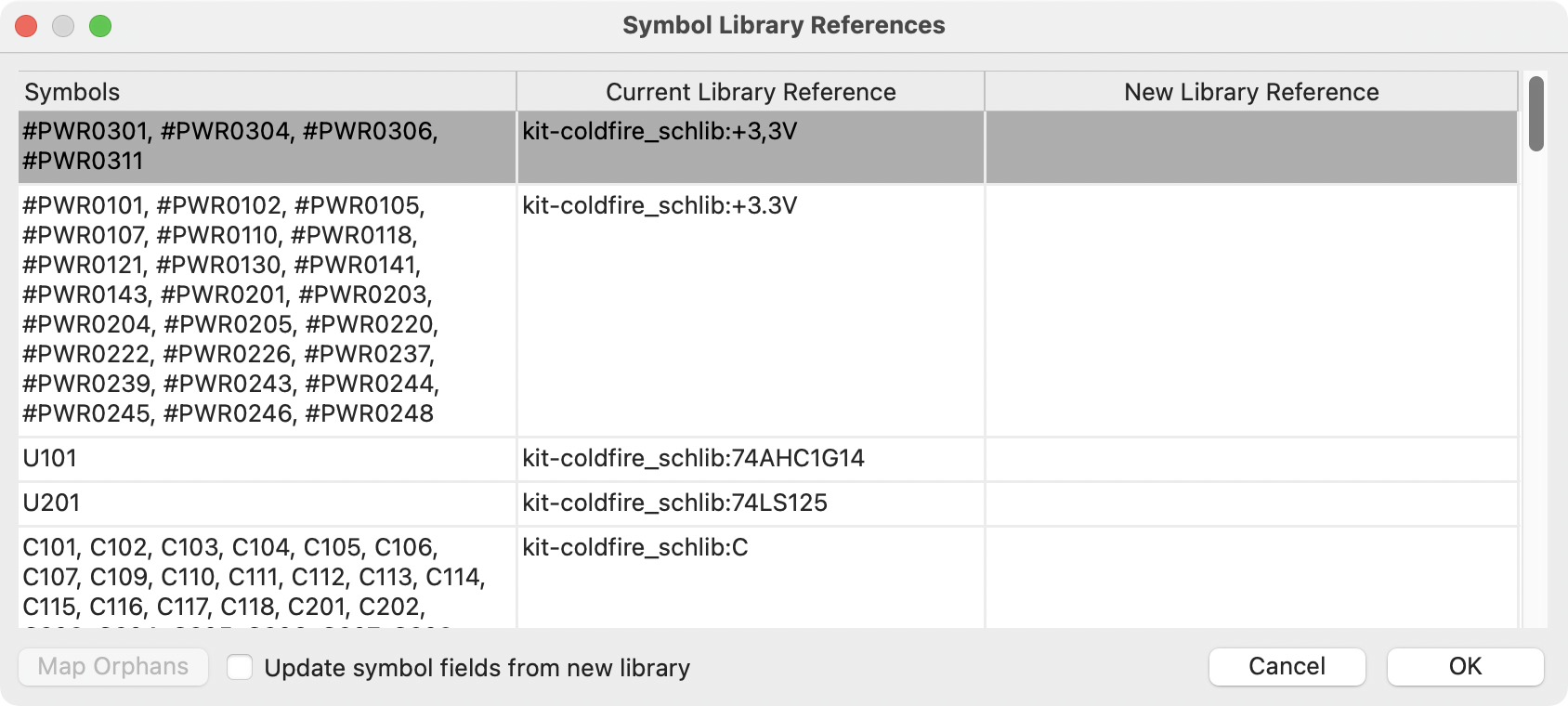
This dialog is primarily useful for managing symbols that appear in multiple libraries, when you want to switch from one library to another. For example, if a schematic uses symbols that are in both a global library and a project-specific library, the Symbol Library References dialog could be used to switch between using the global symbols or the equivalent project-specific symbols. It does not have features for fine-grained control of how fields are updated; for that, use the Change Symbols dialog.
Comparing symbols between schematic and library
When a symbol in a schematic diverges from the corresponding symbol in the original symbol library, you can use the Compare Symbol with Library tool to inspect the differences between the two versions of the symbol. Run the tool using Inspect → Compare Symbol With Library.
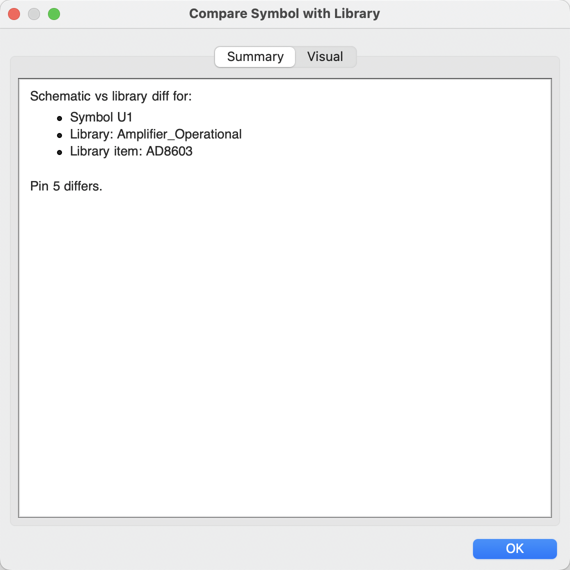
The Summary tab shows the name of the symbol, including its library and schematic reference designator, and provides a list of the differences between the schematic and library versions of the symbol.
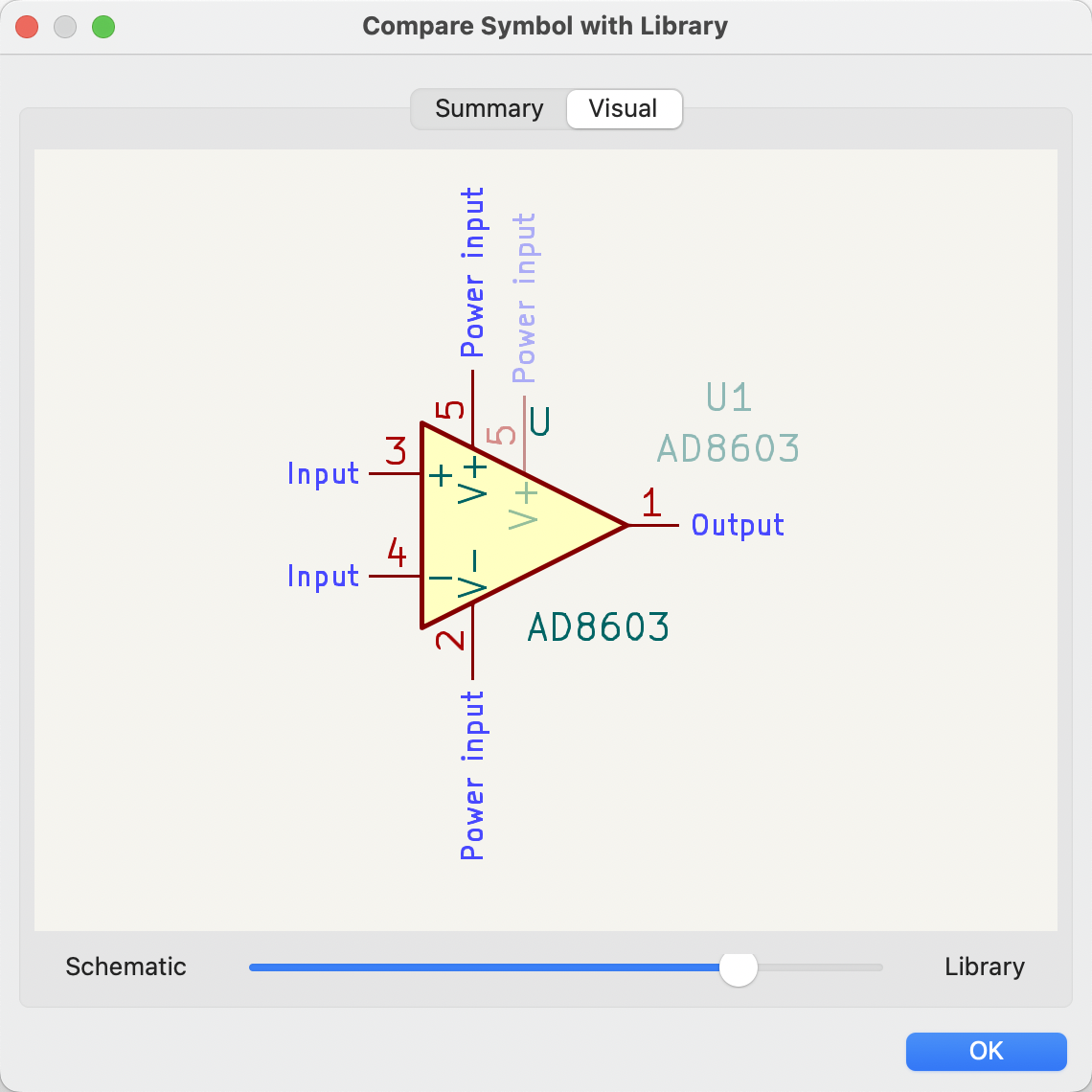
The Visual tab shows a visual comparison of the schematic and library versions of the symbol. This can be used as a visual diff tool.
By default, the comparison displays both versions of the symbol superimposed on each other. To see the changes more easily, you can drag the slider at the bottom of the tab to the right to emphasize the library version of the symbol in the superimposed view (making the schematic version of the symbol more transparent) or drag it to the left to emphasize the schematic version (making the library version more transparent). At the far right and left ends of the slider, the schematic and library versions of the symbol, respectively, are fully hidden. It may be helpful to drag the slider back and forth to see the changes more clearly.
You can press the A/B button, or use the / hotkey, to quickly toggle back and forth between the schematic and library versions.
The Update Symbol from Library… button opens the Update Symbol from Library tool to update the symbol to match the library.
The screenshot above shows a visual comparison with the schematic version of the symbol deemphasized. You can see a partially transparent pin 5 (from the schematic version of the symbol) is in a different location than the fully opaque pin 5 (from the library symbol). This indicates that the pin was moved in either the schematic or library version of the symbol.
Symbol Fields Table
The Symbol Fields Table allows you to view and modify field values for all symbols in a spreadsheet interface. The Symbol Fields Table also acts as a BOM export tool. You can open the Symbol Fields Table with the ![]() button.
button.
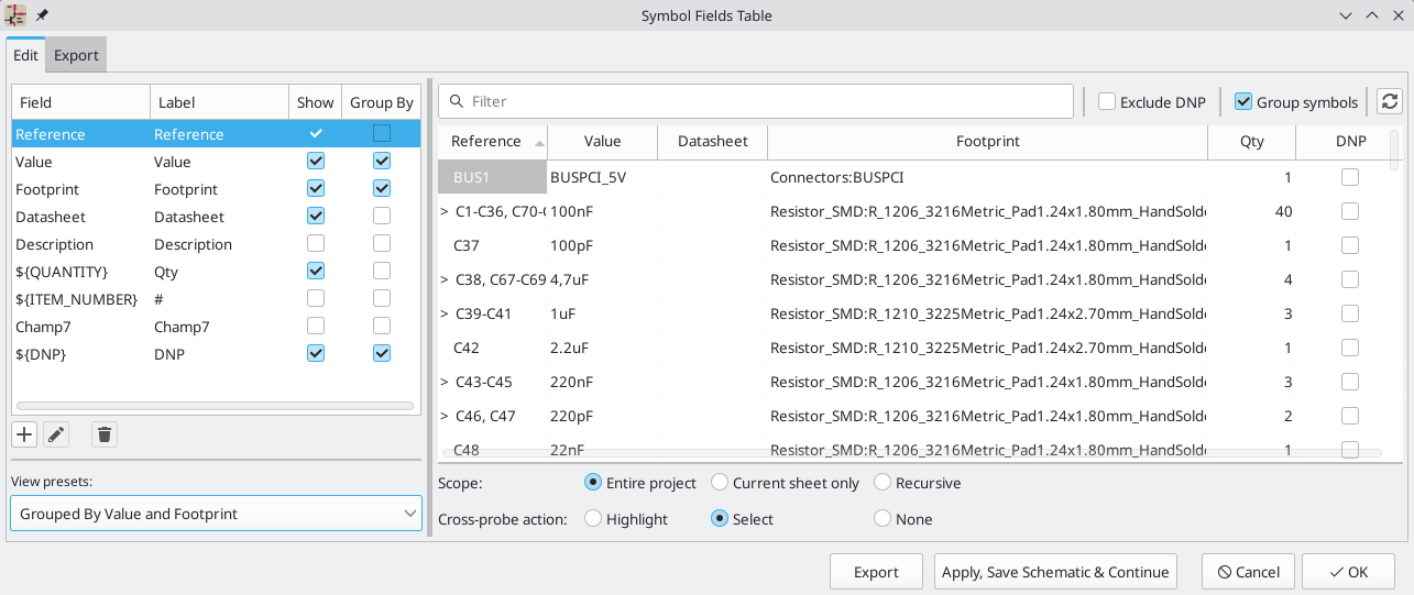
The main table has a row for each symbol and a column for each field. Each cell is editable.
Symbol fields that contain text variables, such as a field set to ${VALUE},
are displayed in the table as their resolved value.
Clicking on the cell to edit it shows the unresolved text variable.
Such cells are shown with a yellow background to indicate the field contains a text variable.
|
Cells are navigated with the arrow keys, or with Tab / Shift+Tab to move right / left and Enter to move down, respectively.
A range of cells can be selected by clicking and dragging. The whole range of selected cells will be copied (Ctrl+C) or pasted into (Ctrl+V) on a copy or paste action. Copying a range of cells from the table can be useful for creating a BOM. More details of copying and pasting cells are described below.
The left pane contains a list of all available symbol fields, as well as some virtual fields such as Quantity and Item Number. You can add or remove any symbol field from the main table on using the Include checkboxes (fields can also be shown or hidden by right-clicking on the header of the main table). New symbol fields can be added using the ![]() button; a field with that name will be added to every symbol. To rename the field, which changes the field name in all symbols, use the
button; a field with that name will be added to every symbol. To rename the field, which changes the field name in all symbols, use the ![]() button. The
button. The ![]() button deletes the field from all symbols. You can collapse this panel by clicking the
button deletes the field from all symbols. You can collapse this panel by clicking the ![]() button.
button.
Each field has its own column label, which is displayed at the top of the corresponding column in the symbol fields table and in exported BOMs. The column label for each field is shown in the second column of in the left pane. A column label does not have to match the field name. To change a field’s column label, click in the BOM Name column for that field, then enter a new name.
Similar symbols can optionally be grouped by any symbol field using the Group By checkboxes. Symbols are grouped into a single row in the table if all of their Group By fields are identical. The grouped row can be expanded to show the individual symbols by clicking the arrow at the left of the row. The Group symbols checkbox enables or disables symbol grouping, and the ![]() button recalculates groupings.
button recalculates groupings.
Presets are available to configure the list of fields. Presets store which fields are displayed, which fields are used for grouping, and the column order. You can create and save your own presets or use one of several default presets. Custom presets can be deleted in this dialog or in the Schematic Setup dialog.
Symbols can be filtered by reference designator using the Filter textbox at the top. The filter supports wildcards: * matches any number of any characters, including none, and ? matches any single character.
You can also change the display scope using the dropdown menu to the right of the filter box. You can show only symbols in the current sheet, the current sheet and all of its subsheets, or the entire project.
The ![]() menu contains some additional options for showing or hiding symbols.
menu contains some additional options for showing or hiding symbols.
-
Include 'DNP' Symbols includes or excludes symbols with the Do Not Populate attribute from both the Edit tab and any BOM exports.
-
Include 'Exclude from BOM' Symbols includes or excludes symbols with the Exclude from BOM attribute from the Edit tab. Symbols with the Exclude from BOM attribute are always excluded from BOM exports.
You can cross-probe from this dialog by selecting a row in the table. Depending on the cross-probe options selected in the ![]() menu, this can highlight the corresponding symbol in the schematic, select the corresponding symbol in the schematic, or do nothing. The selection action can also select the symbol’s footprint in the board editor, depending on the PCB Editor cross-probing settings configured in Preferences.
menu, this can highlight the corresponding symbol in the schematic, select the corresponding symbol in the schematic, or do nothing. The selection action can also select the symbol’s footprint in the board editor, depending on the PCB Editor cross-probing settings configured in Preferences.
The Symbol Fields Table is also a bill of materials tool. You can use the Export button to save the symbol fields to an external file. The fields are exported to the BOM exactly as they are currently shown in the spreadsheet view. File format settings are configured in the Export tab. For more information about exporting a BOM, see the BOM tool documentation.
Virtual fields
If you create a field in the Symbol Fields Table whose name begins with a text variable, a virtual field will be created. Virtual fields have a value that is evaluated for each symbol based on the contents of the field name. For example, a virtual field named ${SYMBOL_NAME} will evaluate to the symbol’s name for each symbol. A virtual field can contain any text, as long as it starts with a text variable, so a virtual field named ${SYMBOL_LIBRARY}:${SYMBOL_NAME} will evaluate to <library name>:<symbol name> for each symbol.
Virtual fields exist only in the Symbol Fields Table and in BOM exports. While they are displayed as a column in the dialog and BOMs, and they can be used to group or sort symbols in BOM exports just like regular fields, adding a virtual field in the Symbol Fields Table does not add a corresponding field to each symbol in the schematic.
Any text variable can be used in virtual fields, including sheet and project text variables.
Text variables that correspond to symbol attributes (${DNP}, ${EXCLUDE_FROM_BOARD}, ${EXCLUDE_FROM_SIM}, ${EXCLUDE_FROM_BOM}) are displayed specially. In the Symbol Fields Table, they are shown as checkboxes for each symbol that directly set or unset the corresponding symbol attribute. In BOM exports, they expand to the friendly name of the attribute if the attribute is set (e.g. Excluded from board for ${EXCLUDE_FROM_BOARD} and DNP for ${DNP}) or to an empty string if the attribute is not set.
Finally, there are two special virtual fields that can be created:
-
${QUANTITY}is a virtual field that contains the number of grouped instances of each symbol. -
${ITEM_NUMBER}is a virtual field that contains the row number of each symbol in the table.
Tricks to simplify filling fields
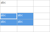
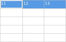
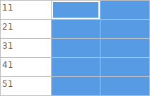
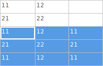
There are several special copy/paste methods in the spreadsheet for pasting values into larger regions, including auto-incrementing pasted cells. These features may be useful when pasting values that are shared in several symbols.
These methods are illustrated below.
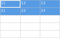
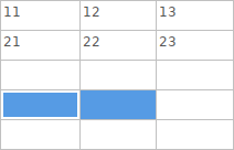
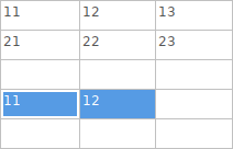
| 1. Copy (Ctrl+C) | 2. Select target cells | 3. Paste (Ctrl+V) |
|---|---|---|
|
|
|
|
|
|
|
|
|
|
|
|
|
|
|
| These techniques are also available in other dialogs with a grid control element. |
Reference designators and symbol annotation
Reference designators are unique identifiers for components in a design. They are often printed on a PCB and in assembly diagrams, and allow you to match symbols in a schematic to the corresponding components on a board.
In KiCad, reference designators consist of a letter indicating the type of component (R for resistor, C for capacitor, U for IC, etc.) followed by a number. If the symbol has multiple units then the reference designator will also have a trailing letter indicating the unit. Symbols that don’t have a reference designator set have a ? character instead of the number. Reference designators must be unique.
Reference designators can be automatically set when symbols are added to the schematic, and you can set or reset reference designators yourself by manually editing an individual symbol’s reference designator field or in bulk using the Annotation tool.
| The process of setting a symbol’s reference designator is called annotation. |
Auto-annotation
When auto-annotation is enabled, symbols will be automatically annotated when they are added to the schematic. You can enable auto-annotation by checking the Automatically annotate symbols checkbox in the Schematic Editor → Editing Options pane in Preferences. Auto-annotation can also be toggled using the ![]() button in the left toolbar.
button in the left toolbar.
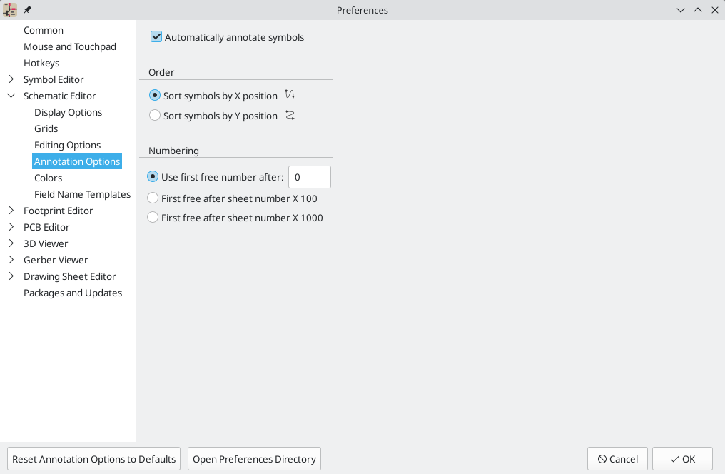
There are options to control how symbols are automatically annotated in the Annotation page of Schematic Setup.
-
When multiple symbols are added simultaneously, they are annotated according to the Order setting, sorted by either X or Y position.
-
The Numbering option sets the starting number for new reference designators. This can be the lowest available number, or a number based on the sheet number. When Allow reference reuse is enabled, reference designators can be automatically assigned as long as they are not currently used by another symbol. When disabled, a reference designator can never be used again once it has been assigned to a symbol, even if it is not currently in use.
For more information about annotation options, see the documentation for the Annotation page of Schematic Setup.
Herramienta de Anotado
The Annotation tool assigns reference designators to symbols in the schematic. To launch the Annotation tool, click the ![]() button in the top toolbar.
button in the top toolbar.
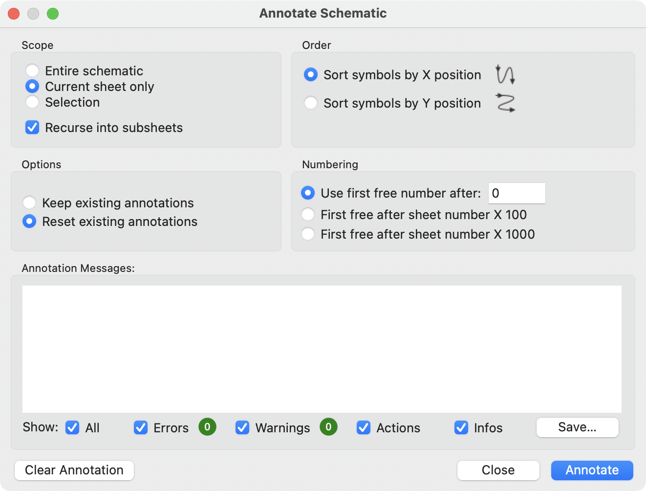
The tool provides several options to control how symbols are annotated.
Scope: Selects whether annotation is applied to the entire schematic, to only the current sheet, or to only the selected symbols. If the Recurse into subsheets option is selected, symbols in subsheets of the selected scope will be reannotated; otherwise symbols in subsheets will not be reannotated. For example, if Recurse into subsheets and Selection only selected, symbols in any selected subsheets will be reannotated.
Options: Selects whether annotation should apply to all symbols and reset existing reference designators, or apply only to unannotated symbols. If the Reset symbol units option is enabled, symbol units will be reannotated individually. This means symbol units may be grouped into symbols differently after reannotation. When it is disabled, each symbol’s units will be reannotated as a group so that they remain together as units of the same symbol.
Order: Chooses the direction of numbering. If symbols are sorted by X position, all symbols on the left side of a schematic sheet will be lower numbered than symbols on the right side of the sheet. If symbols are sorted by Y position, all symbols on the top of a sheet will be lower numbered than symbols at the bottom of the sheet.
Numbering: Selects the starting point for numbering reference designators. The lowest unused number above the starting point is picked for each reference designator. The starting point can be an arbitrary number (typically zero), or it can be the sheet number multiplied by 100 or 1000 so that each part’s reference designator corresponds to the schematic page it is on.
The Clear Annotation button clears all reference designators in the selected scope.
Annotation messages can be filtered with the checkboxes at the bottom or saved to a report using the Save… button.
Electrical connections
Electrical connections in KiCad are known as nets, where each net represents a circuit node. All symbol pins on the same net are considered electrically connected.
There are two primary ways to establish connections: wires and labels. Wires make direct connections between symbol pins and other wires, while labels connect to other labels with the same name. Both wires and labels are shown in the schematic below.
Connections can also be made with buses and with implicit connections via hidden power pins.
Net name assignment rules
Every net in the schematic is assigned a name, whether that name is specified by the user (using a label) or automatically generated by KiCad.
When multiple labels are attached to the same net, the final net name is determined in the following order, from highest priority to lowest:
-
-
Output sheet pins are higher priority than Input sheet pins
-
If there are multiple labels of one type attached to a net, the names are sorted alphabetically and the first is used.
If a net travels through multiple sheets of a hierarchy, it will take its name from the highest level of the hierarchy where it has a hierarchical label or local label. As usual, local labels take priority over hierarchical labels.
If none of the label types above are attached to a net, the net’s name is automatically generated based on the connected symbol pins.
Wires
Wires are used to directly establish electrical connections between two points. To establish a connection, a segment of wire must be connected by its end to another segment or to a pin. Only wire ends create connections; if a wire crosses the middle of another wire, a connection will not be made.
Unconnected wire ends have a small square that indicates the connection point. The square disappears when a connection is made to the wire end. Unconnected pins have a circle, which also disappears when a connection is made.
| Wires connect with other wires or pins only if their ends coincide exactly. Therefore it is important to keep symbol pins and wires aligned to the grid. It is recommended to always use a 50 mil grid when placing symbols and drawing wires because the KiCad standard symbol library and all libraries that follow its style also use a 50 mil grid. |
| Symbols, wires, and other elements that are not aligned to the grid can be snapped back to the grid by selecting them, right clicking, and selecting Align Elements to Grid. |
Drawing and editing wires
To begin connecting elements with wire, use the Wire tool ![]() in the right toolbar (w). Wires can also be automatically started by clicking on an unconnected symbol pin or wire end.
in the right toolbar (w). Wires can also be automatically started by clicking on an unconnected symbol pin or wire end.
You can restrict wires to 90 degree angles using the ![]() button in the left toolbar, or to 45 degree angles with the
button in the left toolbar, or to 45 degree angles with the ![]() button. The
button. The ![]() button allows you to place wires at any angle. You can cycle through these modes using Shift+Space, or select the desired mode in Preferences → Schematic Editor → Editing Options. These modes affect graphic lines in addition to wires.
button allows you to place wires at any angle. You can cycle through these modes using Shift+Space, or select the desired mode in Preferences → Schematic Editor → Editing Options. These modes affect graphic lines in addition to wires.
As in the PCB editor, the / hotkey switches wire posture.
Wires can be moved and edited using the Move (M) or Drag (G) tools. As with symbols, the Move tool moves only the selected segment, without maintaining existing connections to other segments. The Drag tool maintains existing connections.
You can select connected wires using the Select Connection tool (Ctrl+4). This tool selects all connected wire segments until it reaches a junction, starting with the selected segment or the segment under the cursor. Using the tool again expands the existing selection to the next junction.
You can break a wire segment into two pieces by right-clicking a wire and selecting Slice. The segment will be separated at the current mouse position. You can also separate a wire segment from the adjacent segments by right-clicking the segment and selecting Break.
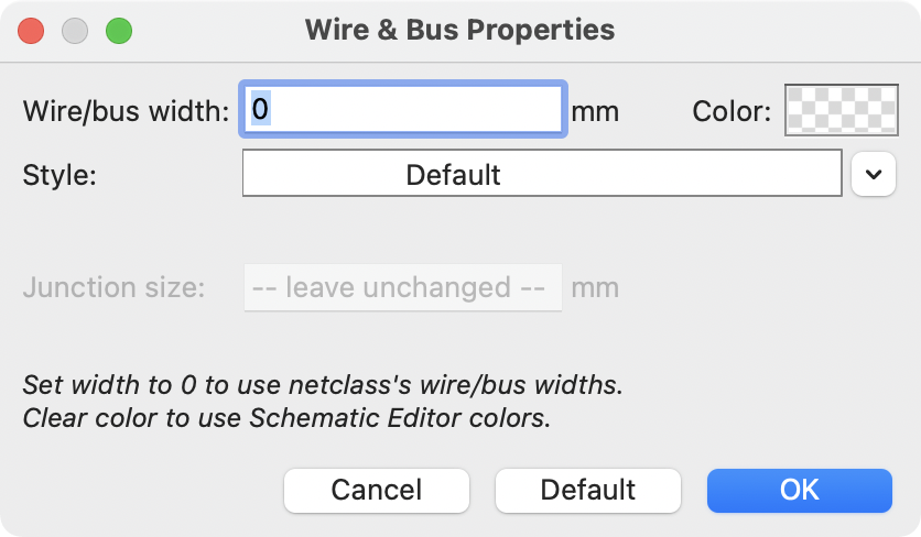
Normally the line style of a wire follows the net’s net class settings (nets are in the Default net class if no other net class is specified). However, the line style for the selected wire segments can be overridden in the wire’s properties dialog (E when a wire segment is selected). The wire’s width, color, and line style (solid, dashed, dotted, etc.) can be set. Setting the width to 0, clearing the color, and using the Default line style uses the default width, color, and style, respectively, from the net class settings. If a wire junction is included in the selection, the junction size can also be edited here.
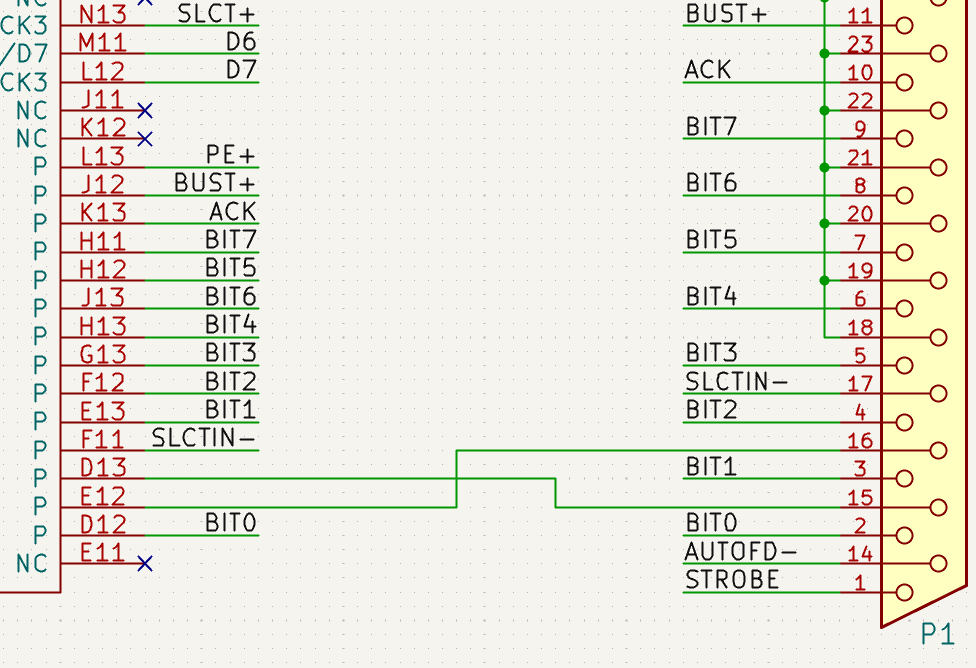
Wire junctions
Wires that cross are not implicitly connected. It is necessary to join them by explicitly adding a junction dot if a connection is desired (![]() button in the right toolbar). Junction dots will be automatically added to wires that start or end on top of an existing wire.
button in the right toolbar). Junction dots will be automatically added to wires that start or end on top of an existing wire.
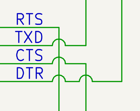
Junction dots are used in the schematic figure above on the wires connected to P1 pins 18, 19, 20, 21, 22, and 23.
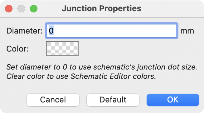
Junction size automatically follows the schematic’s Junction dot size setting in Schematic Setup → General → Formatting. Color follows the net class setting. The automatic size and color can be overridden in each junction dot’s properties; a size of 0 is equivalent to the schematic default size, and clearing the color uses the net class color.
Wire hop-overs
When wires cross without a junction dot, they do not connect. By default, this is drawn simply as one wire crossing through the other wire. However, you can configure such crossovers to be visually indicated with hop-overs instead of simple intersections, as shown in the schematic below. The size of hop-overs is configurable for a given schematic; all hop-overs in the schematic have the same size.
To enable display of hop-overs, open the Formatting page of Schematic Setup and change the Hop-over size setting from None to another size.
Labels
Labels are used to assign net names to wires and pins. Wires with the same net name are considered to be connected, so labels can be used to make connections without drawing direct wire connections.
A net can only have one name. If two different labels are placed on the same net, an ERC violation will be generated. Only one of the net names will be used in the netlist. The final net name is determined according to the rules described below.
There are three types of labels, each with a different connection scope.
-
Local labels, also referred to simply as labels, only make connections within a sheet. Add a local label with the
 button in the right
toolbar.
button in the right
toolbar. -
Global labels make connections anywhere in a schematic, regardless of sheet. Add a global label with the
 button in the right
toolbar.
button in the right
toolbar. -
Hierarchical labels connect to hierarchical sheet pins and are used in hierarchical schematics for connecting child sheets to their parent sheet. Add a hierarchical label with the
 button in the right toolbar.
| Labels that have the same name will connect, regardless of the label type, if they are in the same sheet. |
| You can convert from one type of label to another type of label using the Change To tools. |
Adding and editing labels
After using the appropriate button or hotkey to create a label, the Label Properties dialog appears.
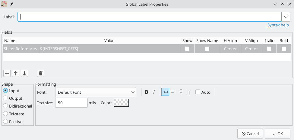
The Label field sets the label’s name, which determines the net that the label assigns to its attached wire or pin. You can choose a label name from a list of nets that are already in the schematic by clicking the dropdown menu next to the label name field.
| Net names can contain any character, including spaces and other special characters. |
Label text supports markup for overbars, subscripts, etc., as well as variable substitution. Use the Syntax help link in the dialog for a summary.
When the Multiple label input option is enabled, the Label field supports entering multiple labels, with one label on each line. In this case, the dialog will create multiple independent labels in sequence, one per line.
| Multiple label input may be useful for copying labels from other sources, such as a spreadsheet. |
There are several options to control the label’s appearance. You can change the font, size, and color of the text, and set bold and italic emphasis. You can also set the orientation of the text relative to the label’s connection point. Hierarchical and global labels have several additional options: the Auto option automatically sets the label orientation based on the connected schematic elements, and Shape option controls the shape of the label outline (Input, Output, Bidirectional, Tri-state, or Passive). The outline shape is purely visual and has no electrical consequence.
| The default text size can be set for a schematic in Schematic Setup, and the default font can be set in Preferences. |
| Global labels have additional settings to control margins around the label text in the Schematic Setup dialog. |
Labels can also have fields added to them. Two fields have special meaning (Net Class and Sheet References, described below), but arbitrary fields can also be added. Label fields behave like symbol fields: you can show or hide their name and value and adjust the alignment, orientation, position, size, font, color, and emphasis.
| Formatting options for label fields can be shown or hidden by right-clicking on the header row of the label field table and enabling or disabling the desired columns. Not all columns are shown by default. |
Like symbol fields, label fields can be edited individually by opening the properties of a specific label field from the schematic (double click the label field, or use E).
After accepting the label properties, the label is attached to the cursor for placement. The connection point for a label is the small square in the corner of the label. The square disappears when the label is connected to a wire or the end of a pin. If multiple labels were specified in the dialog, each label is attached to the cursor for placement after the previous label is placed.

The connection point’s position relative to the label text can be changed by choosing a different label orientation in the label’s properties, or by mirroring/rotating the label.
The Label Properties dialog can be accessed at any time by selecting a label and using the E hotkey, double-clicking on the label, or with Properties… in the right-click context menu.
Assigning net classes with labels
In addition to assigning net names, labels can be used to assign net classes. A label field named Net Class assigns the specified net class to the net associated with the label. To make it easier to assign net classes in this way, Net Class is the default name for new label fields, and Net Class fields present a dropdown list of all the net classes that have been specified in Schematic Setup or Board Setup.
You can also type in a net class that isn’t explicitly listed in the Schematic/Board Setup priority list. Such implicit net classes can’t be assigned any design settings, like net class color or track width, but they can still be used in DRC rule queries.
If multiple Net Class fields are added to a label, or multiple labels with Net Class fields are applied to a net, all of the specified net classes are assigned to the net.
For more information about assigning net classes, see the net class documentation.
Inter-sheet references
Global labels can display inter-sheet references, which are a list of page numbers for other places in the schematic where the same global label appears. Clicking an inter-sheet reference travels to the listed page. If multiple references are listed, clicking the reference list brings up a menu to select the desired page.
Inter-sheet references are globally controlled in the Schematic Setup window’s Formatting page. References can be enabled or disabled, and the displayed format for the list can be adjusted, including with optional prefix or suffix characters.
The image below shows a global label with inter-sheet references to two other schematic pages. A prefix and suffix of [ and ], respectively, were added in Schematic Setup.
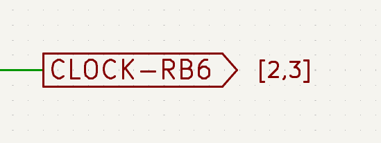
A Sheet References field with value ${INTERSHEET_REFS} is automatically added to global labels, and is used to control the appearance of inter-sheet references for that label. The ${INTERSHEET_REFS} text variable gets expanded to the full list of inter-sheet references for the global label, as configured in Schematic Setup. Visibility of inter-sheet references is globally controlled in Schematic Setup rather than with the Sheet References field visibility control. The Sheet References field has no meaning for other types of labels.
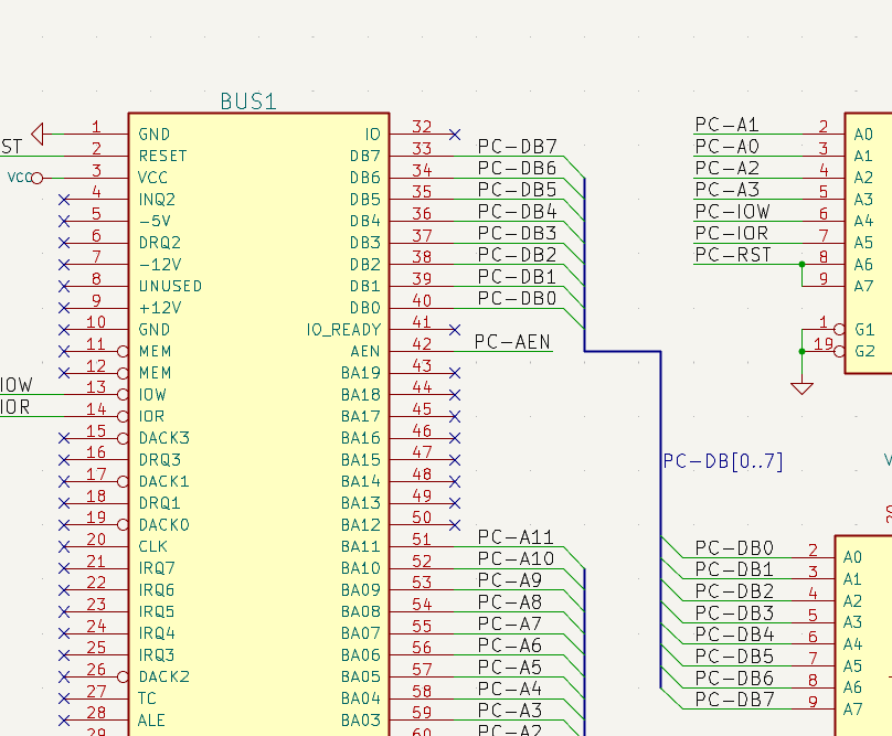
Buses
Buses are a way to group related signals in the schematic in order to simplify complicated designs. Buses can be drawn like wires using the bus tool ![]() , and are named using labels the same way signal wires are.
, and are named using labels the same way signal wires are.
In the following schematic, many pins are connected to buses, which are the thick blue lines in the center.
Miembros del Bus
There are two types of bus in KiCad 6.0 and later: vector buses and group buses.
A vector bus is a collection of signals that start with a common prefix and end with a number. Vector buses are named <PREFIX>[M..N] where PREFIX is any valid signal name, M is the first suffix number, and N is the last suffix number. For example, the bus DATA[0..7] contains the signals DATA0, DATA1, and so on up to DATA7. It doesn’t matter which order M and N are specified in, but both must be non-negative.
Vector bus prefixes cannot contain the characters {, }, [, or ], except as part of markup for superscripts, subscripts, overbars, or text variables. Prefixes may contain spaces, but the spaces must be escaped. You can escape spaces in the prefix either by preceding the space with a backslash (\) or by surrounding the entire prefix with double quotes ("). For example, DATA\ BUS[0..7] and "DATA BUS"[0..7] are both valid vector bus names.
A group bus is a collection of one or more signals and/or vector buses. Group buses can be used to bundle together related signals even when they have different names. Group buses use a special label syntax:
<OPTIONAL_NAME>{SIGNAL1 SIGNAL2 SIGNAL3}
The members of the group are listed inside curly braces ({}) separated by space characters. An optional name for the group goes before the opening curly brace. If the group bus is unnamed, the resulting nets on the PCB will just be the signal names inside the group. If the group bus has a name, the resulting nets will have the name as a prefix, with a period (.) separating the prefix from the signal name.
For example, the bus {SCL SDA} has two signal members, and in the netlist these signals will be SCL and SDA. The bus USB1{DP DM} will generate nets called USB1.DP and USB1.DM. For designs with larger buses that are repeated across several similar circuits, using this technique can save time.
Group buses can also contain vector buses. For example, the bus MEMORY{A[7..0] D[7..0] OE WE} contains both vector buses and plain signals, and will result in nets such as MEMORY.A7 and MEMORY.OE on the PCB.
Group bus names cannot contain the characters {, }, [, or ], except as part of markup for superscripts, subscripts, overbars, or text variables. Group bus names and the constituent net names may contain spaces, but the spaces must be escaped. You can escape spaces either by preceding the space with a backslash (\) or by surrounding the entire group bus name or net name with double quotes ("). For example, DATA\ BUS{SIGNAL\ 1 SIGNAL\ 2}, "DATA BUS"{"SIGNAL 1" "SIGNAL 2"}, and "DATA BUS"{SIGNAL\ 1 "SIGNAL 2"} are all valid (and equivalent) labels for group buses.
Bus wires can be drawn and connected in the same manner as signal wires, including using junctions to create connections between crossing wires. Like signals, buses cannot have more than one name — if two conflicting labels are attached to the same bus, an ERC violation will be generated.
Conexión entre miembros de bus
Pins connected between the same members of a bus must be connected by labels. It is not possible to connect a pin directly to a bus; this type of connection will be ignored by KiCad.
En el ejemplo anterior, las conexiones son realizas por las etiquetas colocadas sobre los hilos conectados a los pines. Las entradas de bus (segmentos de hilo a 45 grados) son solo representaciones gráficas, y no forman necesariamente conexiones lógicas.
In fact, using the repetition command (Insert), connections can be very quickly made in the following way, if component pins are aligned in increasing order (a common case in practice on components such as memories, microprocessors…):
-
Place the first label (for example
PCA0) -
Use the repetition command as much as needed to place members. KiCad will automatically create the next labels (
PCA1,PCA2…) vertically aligned, theoretically on the position of the other pins. -
Dibuje el hilo bajo la primera etiqueta. Después utilice el comando repetir para colocar los otros hilos bajo el resto de etiquetas.
-
Si fuera necesario, coloque las entradas al bus del mismo modo (coloque la primera entrada y utilice el comando repetir)
|
In the Schematic Editor → Editing Options section of the Preferences menu, you can set the repetition parameters:
|
Bus unfolding
The unfold tool allows you to quickly break out signals from a bus. To unfold a signal, right-click on a bus object (a bus wire, etc) and choose Unfold from Bus. Alternatively, use the Unfold Bus hotkey (default: C) when the cursor is over a bus object. The menu allows you to select which bus member to unfold.
After selecting the bus member, the next click will place the bus member label at the desired location. The tool automatically generates a bus entry and wire leading up to the label location. After placing the label, you can continue placing additional wire segments (for example, to connect to a component pin) and complete the wire in any of the normal ways.
Bus aliases
Bus aliases are shortcuts that allow you to work with large group buses more efficiently. They allow you to define a group bus and give it a short name that can then be used instead of the full group name across the schematic.
To create bus aliases, open the Bus Alias Definitions pane in Schematic Setup.
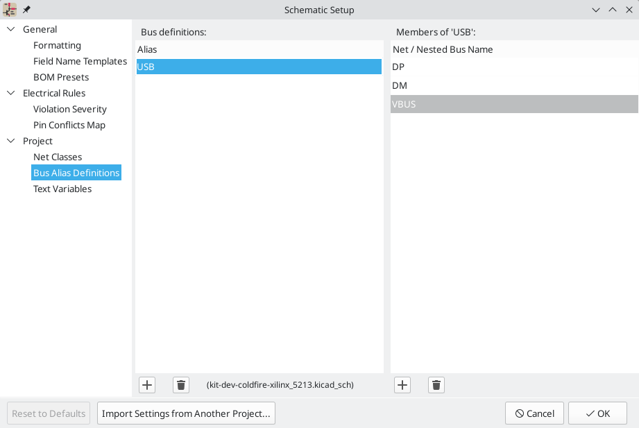
An alias may be named any valid signal name. Using the dialog, you can add signals or vector buses to the alias. As a shortcut, you can type or paste in a list of signals and/or buses separated by spaces, and they will all be added to the alias definition. In this example, we define an alias called USB with members DP, DM, and VBUS.
After defining an alias, it can be used in a group bus label by putting the alias name inside the curly braces of the group bus: {USB}. This has the same effect as labeling the bus {DP DM VBUS}: the nets will be DP, DM, and VBUS. You can also add a prefix name to the group, such as USB1{USB}, which results in nets such as USB1.DP. For complicated buses, using aliases can make the labels on your schematic much shorter. Keep in mind that the aliases are just a shortcut, and the name of the alias is not included in the netlist.
Bus aliases are saved in the schematic file that is opened when the alias is created. The Bus Alias Definitions window shows the schematic file associated with the selected alias at the bottom of the alias list. Any aliases created in a given schematic sheet are available to use in any other schematic sheet that is in the same hierarchical design. If multiple sheets in a hierarchical design contain identically-named bus aliases, the aliases must all have the same members. ERC will report a violation if multiple bus aliases with the same name do not have consistent members.
Bus example
In the schematic below, a bus alias named USB is defined with members DP, DN.
The root sheet has three buses, one with label {USB}, with no prefix, and two with prefixes: USB1{USB} and USB2{USB}. The first bus results in nets DP and DN, the second results in nets USB1.DP and USB1.DN, and the third results in nets USB2.DP and USB2.DN.
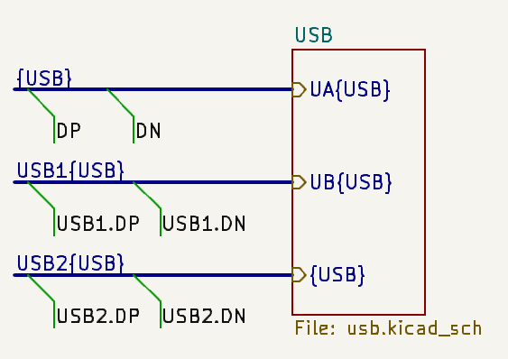
When connecting to a sub-sheet, the hierarchical labels (and therefore hierarchical sheet pins) are named with the same syntax. They need the same members as the connected bus. As for bus labels, hierarchical labels can define a prefix or not. In this case, the hierarchical labels are named {USB} (i.e. no prefix) and UA{USB} and UB{USB}.
Within the subsheet, the hierarchical labels for the bus are what define the prefixes of displayed labels of unfolded bus members on that sheet. However, the nets resolve according to the connectivity with the parent sheet.
For example, the bus member labeled UB.DP in the subsheet has the label prefix UB due to the hierarchical label, and the resolved net name /USB1.DP due to the name of the bus in the parent sheet that connects to that hierarchical label.
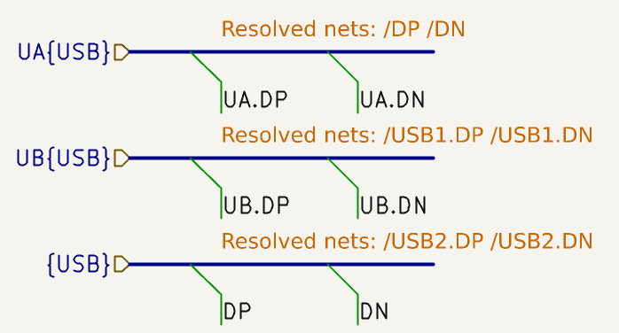
Buses with more than one label
KiCad 5.0 and earlier allowed the connection of bus wires with different labels together, and would join the members of these buses during netlisting. This behavior has been removed in KiCad 6.0 because it is incompatible with group buses, and also leads to confusing netlists because the name that a given signal will receive is not easily predicted.
If you open a design that made use of this feature in a modern version of KiCad, you will see the Migrate Buses dialog which guides you through updating the schematic so that only one label exists on any given set of bus wires.
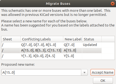
For each set of bus wires that has more than one label, you must choose the label to keep. The drop-down name box lets you choose between the labels that exist in the design, or you can choose a different name by manually entering it into the new name field.
Power symbols
Power symbols are symbols that are conventionally used to represent a connection to a power net, such as VCC or GND. Power symbols are virtual: they do not represent a physical component on the PCB.
In addition to being a visual indicator that the attached net is a power rail, power symbols make global connections: two power symbols with the Value connect to each other anywhere in the schematic, regardless of sheet. The power symbol’s Value field determines the name of the attached net.
| In previous versions of KiCad, power symbols used invisible power input pins, which make implicit global connections based on the pin name as described below. Beginning in KiCad 8, power symbols do not need to use invisible pins, and the global connection is made based on the power symbol’s value. |
In the figure below, power symbols are used to connect the positive and negative terminals of the capacitors to the VCC and GND nets, respectively.
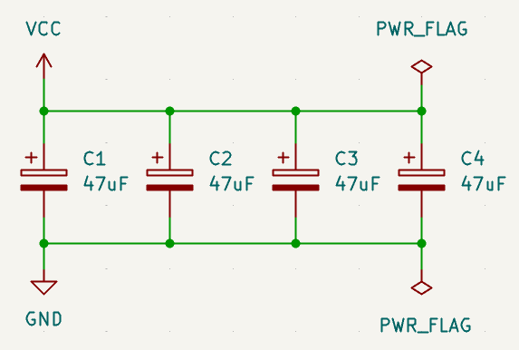
In the KiCad standard library, power symbols are found in the power library, but power symbols can be created in any library. Creating custom power symbols is described in the symbol editor documentation. Instead of making a new symbol, you can also modify an existing power symbol in the schematic: changing its Value field will change the net the power symbol connects to.
PWR_FLAG
Two PWR_FLAG symbols are visible in the screenshot above. They indicate to ERC that the two power nets VCC and GND are actually connected to a power source, as there is no explicit power source such as a voltage regulator output attached to either net.
Without these two flags, the ERC tool would diagnose: Error: Input Power pin not driven by any Output Power pins.
The PWR_FLAG symbol is found in the power symbol library. The same effect can be achieved by connecting any power output pin to the net.
Hidden power pins
When the power pins of a symbol are visible, they must be connected, as with any other signal. However, symbols are sometimes drawn with hidden power input pins, which are connected implicitly. KiCad automatically connects invisible pins with type Power Input to a global net with the same name as the pin. For example, if a symbol has a hidden power input pin named VCC, this pin will be globally connected to the VCC net on all sheets. This kind of implicit connection is not recommended in new designs.
| Care must be taken with hidden power input pins because they can create unintentional connections. By nature, hidden pins are invisible and do not display their pin name. This makes it easy to accidentally connect two power pins to the same net. For this reason, using invisible power pins in symbols is not recommended and is only supported for compatibility with legacy designs and symbols. |
|
Hidden pins can be shown in the schematic by checking the Show hidden
pins option in the Schematic Editor → Display Options section
of the preferences, or by selecting View → Show hidden pins.
There is also a toggle icon |
No-connection flags
No-connection flags (![]() ) are used to indicate that a pin is intentionally unconnected. These flags prevent "unconnected pin" ERC warnings for pins that are intentionally unconnected. Also, while symbol pins that are stacked on top of each other are normally connected to the same net, if a no-connection flag is added to the stacked pins they will instead be connected to separate nets.
) are used to indicate that a pin is intentionally unconnected. These flags prevent "unconnected pin" ERC warnings for pins that are intentionally unconnected. Also, while symbol pins that are stacked on top of each other are normally connected to the same net, if a no-connection flag is added to the stacked pins they will instead be connected to separate nets.
Note that no-connection flags are distinct from the "unconnected" symbol pin type, although they both prevent "unconnected pin" ERC warnings on the pin in question and prevent stacked pins from connecting to each other.
Net classes
Net classes are named groupings of nets that can be assigned design rules (for the PCB) and graphical properties (for the schematic).
More than one net class can be assigned to a net (through a combination of graphical assignments and net class patterns). For nets with multiple net classes assigned, an effective aggregate net class is formed, taking any net class properties from the highest priority net class which has that property set. Net class priority is determined by the ordering in the Schematic or Board Setup dialogs. The Default net class is used as a fallback for any missing properties after all explicit net classes have been considered; this means that nets may be part of the Default net class even if they have other net classes explicitly assigned.
Net classes may be created and edited in either the Schematic or Board Setup dialogs. Nets can be added to net classes in either the schematic or board using pattern-based assignments described below. Nets can also be assigned to net classes in the schematic using graphical assignments with net class directives or net labels.
Selecting a wire or label displays the net’s net class in the message panel at the bottom of the window.
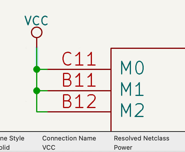
Managing net classes in Schematic Setup
Net classes are managed in the Net Classes panel of the Schematic Setup dialog.
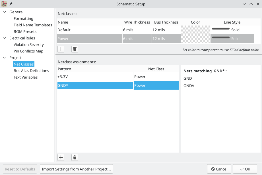
The top pane lists the net classes that exist in the design. The Default net class always exists, and you can add additional net classes with the ![]() button or remove the selected net class with the
button or remove the selected net class with the ![]() button.
button.
Net classes can be moved up and down in priority order with the ![]() and
and ![]() buttons. Note that the
buttons. Note that the Default net class will always be the lowest priority net class and can therefore not be moved.
Each net class can have unique graphic properties that determine how wires of that net class are displayed in the schematic. Wire and bus thicknesses, color, and line style (solid, dashed, dotted, etc.) can all be adjusted. Setting the color to transparent will use the theme’s default wire/bus color for the net class, which is configurable in Preferences. By default any color that is configured for a net class controls the color is used to draw wires in that net class. If the Highlight netclass colors setting is enabled in the Display Options section of the Schematic Editor preferences, this color will instead be used to draw a highlight around wires in that netclass, and the wires themselves will always be drawn with the color scheme’s wire color.
You can also set board design rules for each net class, although the DRC fields are hidden by default. Right click the header row to show or hide additional columns. For more information about setting net class design rules, see the PCB editor documentation.
All net class parameters for user-defined net classes are optional. However, all properties belonging to the Default net class must be set. When a net has more than one net class assigned, the appropriate value for graphic properties or board design rules is taken from the highest priority assigned net class with the relevant value set. If only one net class is assigned which contains missing properties, any missing values will be taken from the Default net class.
The bottom pane lists pattern-based net class assignments. Each row has a net name pattern and a net class; nets with names that match the pattern are assigned to the specified net class. If a net matches multiple patterns, the net is assigned to all of the matching net classes. You can sort the list of net class assignment patterns by pattern or by net class name by clicking on the corresponding column header.
Pattern-based net class assignments are dynamic: when a new net is added that matches an existing pattern, it will be assigned to the associated net class automatically. Net patterns can use both wildcards (* to match any number of any characters, including none, and ? to match any character) and regular expressions. The nets that match the selected pattern are displayed to the right of the pattern list.
For example, the net* pattern matches nets named net, net1, network, and any other net name beginning with net. Because * has a slightly different meaning in a regular expression (* matches zero or more of the preceding character), the net* pattern would also match a net named ne.
Remember that net names must include the full sheet path. For example, a
locally labeled net in the root sheet has a name prefixed with /.
|
Use the ![]() button to add a net class assignment pattern or the
button to add a net class assignment pattern or the ![]() button to remove a pattern.
button to remove a pattern.
Instead of adding net class patterns in the Schematic Setup dialog, you can directly create net class patterns from the schematic canvas. Right click a net and select Assign Netclass… to bring up the Add Netclass Assignment dialog. The net class pattern is pre-filled with the name of the selected net, but the pattern can be changed if desired. All nets matching the pattern are displayed in the dialog. This method can only be used on nets with an assigned name.
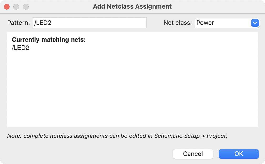
Graphically assigning net classes in the schematic
As an alternative to pattern-based net class assignment, net classes can be graphically assigned to nets in the schematic using either directive labels, net labels, or rule areas.
In the image below, a directive label is used to assign signals to the 50R net class.
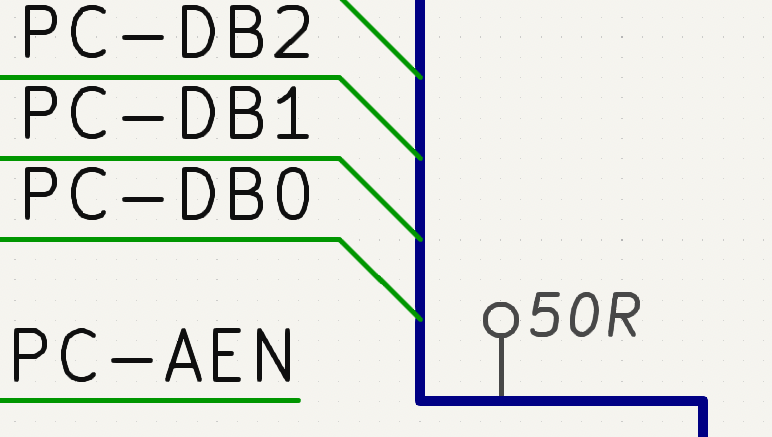
Directive labels are added with the ![]() button in the right toolbar. They behave like labels, except that they cannot be used to name a net. The attached net is assigned a net class according to the value of the directive’s
button in the right toolbar. They behave like labels, except that they cannot be used to name a net. The attached net is assigned a net class according to the value of the directive’s Net Class field. The Net Class field presents a dropdown list of all the net classes that have been specified in Schematic Setup or Board Setup.
You can also type in a net class that isn’t explicitly listed in the Schematic/Board Setup priority list. Such implicit net classes can’t be assigned any design settings, like net class color or track width, but they can still be used in DRC rule queries.
If multiple Net Class fields are added to a directive label, or multiple directive labels with Net Class fields are applied to a net, all of the specified net classes are assigned to the net.
If a directive is attached to a bus, all members of the bus are assigned to the specified net class.
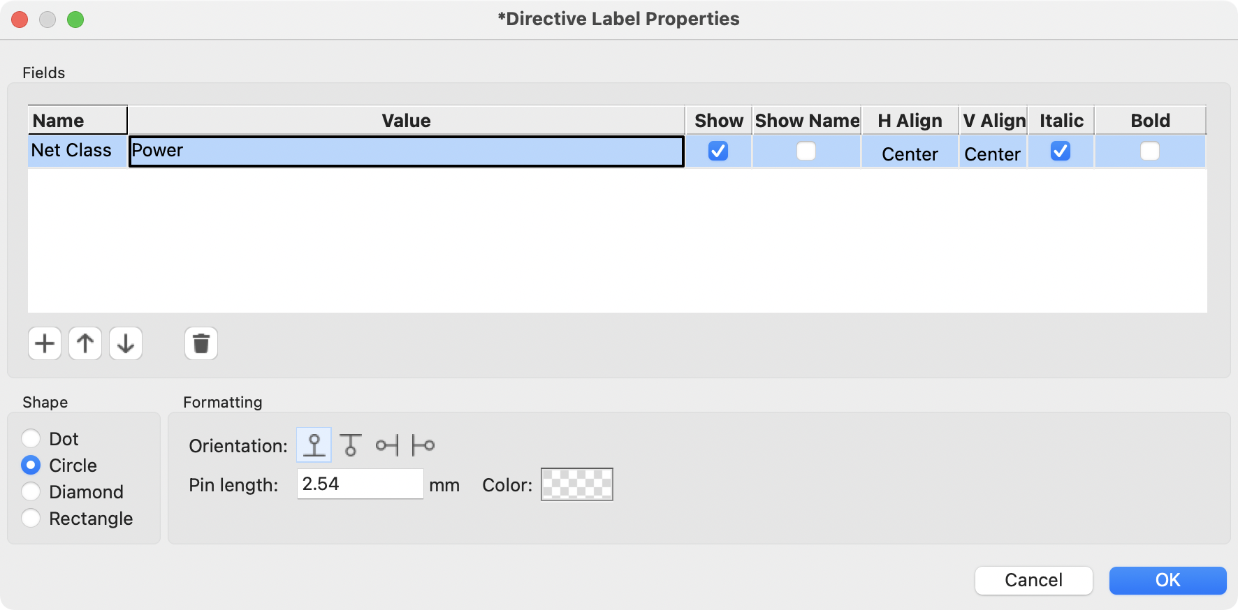
In addition to the associated net class, you can edit the directive’s shape (dot, circle, diamond, or rectangle), orientation, pin length, and color in the directive’s properties.
Net labels can also be used to assign net classes to
nets by adding a Net Class field to the label.
|
The Rule Area tool (![]() ) can be used to draw a shape to which net class directives can be attached. Any wire, bus, label, or symbol pin which crosses or is inside the rule area will be assigned the net class of a net class directive attached to the rule area border. An example is shown in the image below; all wires passing through the rule area will be assigned the
) can be used to draw a shape to which net class directives can be attached. Any wire, bus, label, or symbol pin which crosses or is inside the rule area will be assigned the net class of a net class directive attached to the rule area border. An example is shown in the image below; all wires passing through the rule area will be assigned the RAM_ADDR net class.
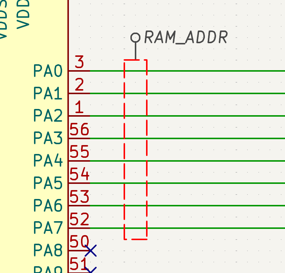
You can show or hide directive labels in the schematic using the View → Show Directive Labels option.
Component classes
Component classes are named groupings of components: they are assigned to symbols in the schematic or to footprints in the board, but however they are assigned they apply to both the symbols and the corresponding footprints. They can be used to group symbols into channels for multichannel designs and can also be used to group footprints in custom DRC rules.
To assign a component class to a symbol, you can add a symbol field named Component Class to the symbol. The symbol will then be a member of the component class named by the field.
You can also assign component classes using directive labels (![]() ) in combination with rule areas (
) in combination with rule areas (![]() ). The Rule Area tool can be used to draw a shape to which directive labels can be attached. Any symbol which crosses or is inside the rule area will be assigned to the component class specified by the directive label attached to the rule area border. An example is shown in the image below; R1 and R2 will be assigned to the
). The Rule Area tool can be used to draw a shape to which directive labels can be attached. Any symbol which crosses or is inside the rule area will be assigned to the component class specified by the directive label attached to the rule area border. An example is shown in the image below; R1 and R2 will be assigned to the Channel 1 component class.
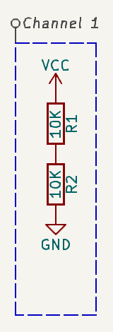
Component classes can also be assigned in the PCB Editor by creating rules for automatic component class assignment.
Components can have more than one class, and symbols take on a class if any of their sub-units have that class. If multiple Component Class fields are added to a directive label, or multiple directive labels with Component Class fields are applied to a rule area, the symbols in the rule area will take on all of the specified component classes.
Rule areas
Rule areas are regions of the schematic that apply certain properties to the symbols and nets inside the area.
You can use rule areas to apply any of the following attributes to the symbols inside the rule area:
-
Exclude from simulation
-
Exclude from bill of materials
-
Exclude from board
-
Do not populate
A rule area that has any of those attributes enabled will apply the enabled attributes to all symbols that are fully or partially enclosed by the rule area.
You can also use a rule area, in combination with a directive label, to apply net classes and component classes to symbols and nets inside the rule area. Any wire, bus, label, or symbol pin which crosses or is inside the rule area will be assigned the net class specified by any directive labels attached to the rule area border. Any symbols that are fully or partially enclosed by the rule area will be assigned the component class specified by any attached directive labels.
In the image below, all wires passing through the rule area will be assigned the RAM_ADDR net class.
To draw a rule area, use the Rule Area tool (![]() button).
button).
-
Click in the canvas to begin drawing the rule area outline.
-
Click to place additional corners.
-
Double click to complete the outline.
The rule area tool obeys the selected line mode: the outline is restricted to horizontal, vertical, and 45 degree lines unless free angle mode is enabled.
|
You can switch line modes using Shift+Space or using the |
To use a rule area to assign a net class or component class, you must add a directive label to the rule area.
-
Activate the directive label tool (
 button on the right toolbar). By default, the directive label tool is grouped in a palette with the other label tools and therefore may be hidden.
 -
In the directive label’s properties dialog, set the label’s
Net Classand/orComponent Classfields to the desired net class or component class, respectively. -
Place the directive label in the canvas so that the label’s connection point is on the border of the rule area, as shown in the screenshot above.
To enable attributes (exclude from simulation, exclude from BOM, exclude from board, or DNP) for the rule area, open the rule area’s properties dialog (E). Any attributes that are enabled in the rule area’s properties are applied to symbols that are fully or partially enclosed by the rule area.
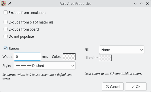
You can also configure the graphical style of the rule area’s border and fill here. The border can be set to any color or line width, and various line styles (solid, dashed, dotted, etc.) are available. If the line width is set to 0, the default line width from the Formatting page of Schematic Setup is used. The fill can be set to None (default), Solid, or one of several types of hatching. You can also configure the fill color. If either the border or fill color is not set, that color is taken from the Rule Areas color in the color theme.
Graphics and text
Text, graphic shapes, and images can be added to schematics for documentation purposes. These items do not have any electrical effect on the schematic.
The image below shows graphic lines and text ("COMMUNICATION DSP") in addition to symbols and several types of labels.
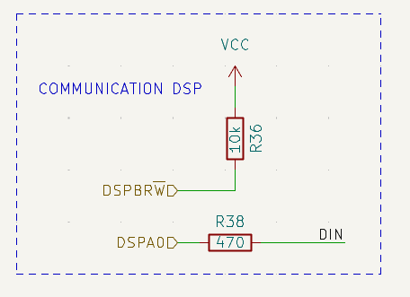
Text and text boxes
Two kinds of text can be added to schematics, which are referred to as text (![]() ) and text boxes (
) and text boxes (![]() ). Both are added using their respective buttons in the right toolbar. Text boxes are similar to regular text except that they have an optional border and they automatically reflow text within that border.
). Both are added using their respective buttons in the right toolbar. Text boxes are similar to regular text except that they have an optional border and they automatically reflow text within that border.
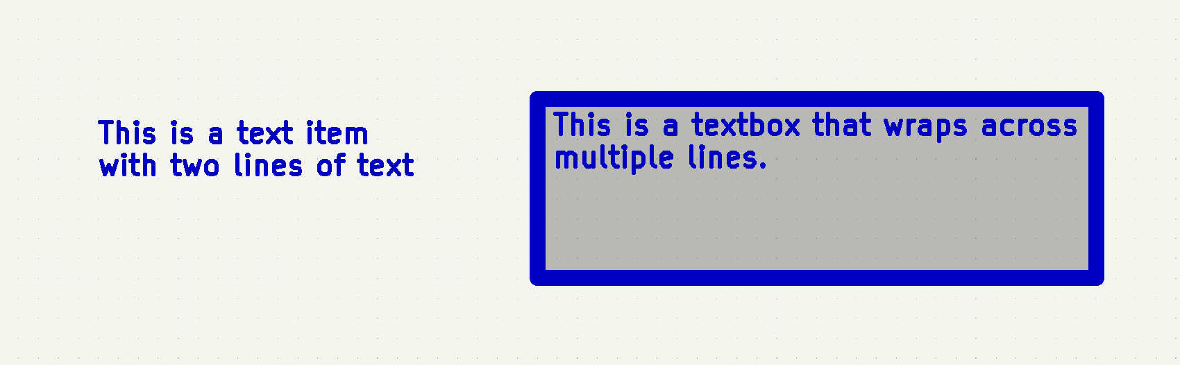
Both kinds of text item support multiline text and basic formatting features, but text boxes wrap text to fit in the outline and have additional formatting options. All text has adjustable fonts, color, size, bold and italic emphasis, left and right alignment, and vertical and horizontal orientation. Text boxes additionally support horizontal centering, vertical alignment options, and colored borders and fill. You can also adjust the padding on each side of text in a text box (padding can be set using the Properties Manager, but not using the Text Box Properties dialog).
| The default text size can be set for a schematic in Schematic Setup, and the default font can be set in Preferences. |
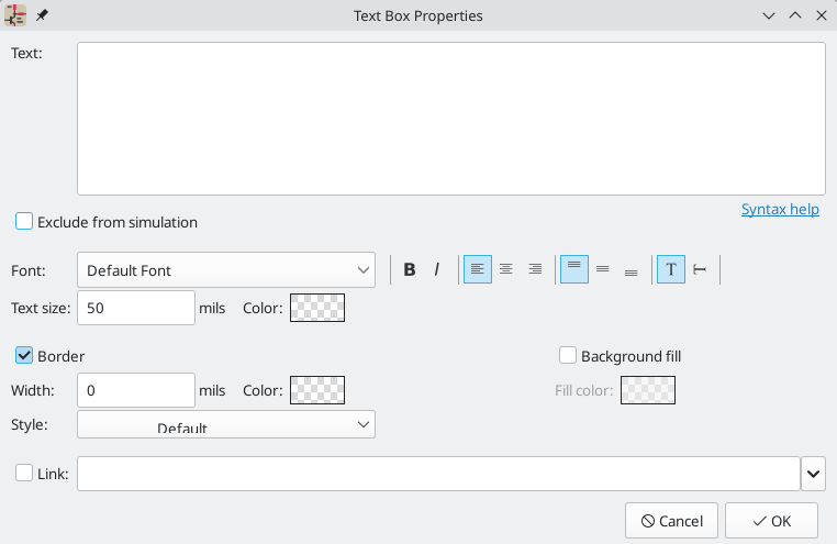
Links
In a text object, text box, or table cell, any text beginning with http:// or https:// is treated as a URL and automatically turned into a link. Clicking on such a link opens the URL in your web browser. If the text contains multiple URLs, each URL is turned into a separate link.
Alternatively, you can explicitly turn an entire text object or text box into a link by entering a target in the Link box in the text properties. This turns the entire text item or text box into a clickable link. Such text can only link to a single URL, but the displayed text can be anything, rather than simply the URL.
You can link to different kinds of resources depending on the link target. The target of an explicit link can be:
-
a sheet in the current schematic, using
#followed by the page number -
a local file on your machine, using a URL with the
file://scheme -
a website, using a URL with the
http://orhttps://scheme -
another resource, using a URL with the appropriate scheme, e.g.
ftp://
If no protocol prefix is used, the target is assumed to be a local file as if the file:// scheme was used.
Sheet, file, and web links can be autofilled using the dropdown meu in the link target box. Other kinds of links cannot be autofilled but will work if your system can handle them.
Fonts
Text and text boxes support custom fonts, which are selectable with the Font dropdown in the properties dialog for the text. In addition to the KiCad font, you can use any TTF font installed on your computer.
| User fonts are not embedded in the project. If the project is opened on another computer that does not have the selected font installed, a different font will be substituted. For maximum compatibility, use the KiCad font. |
Text markup
Text supports markup for superscripts, subscripts, overbars, evaluating project variables, and accessing symbol field values.
| Feature | Markup Syntax | Result |
|---|---|---|
Superscript |
|
textsuperscript |
Subscript |
|
textsubscript |
Overbar |
|
text |
|
variable_value |
|
|
field_value of symbol refdes |
| Project text variables must be defined in Schematic Setup before they can be used. There are also a number of built-in system text variables. |
Simulation directives
Text and textboxes can contain simulation directives for SPICE simulations. The Exclude from simulation checkbox prevents text from being interpreted as a simulation directive.
Tables
You can use a table to organize text in a tabular format. Tables have customizable borders, cell sizes, colors, and headers.
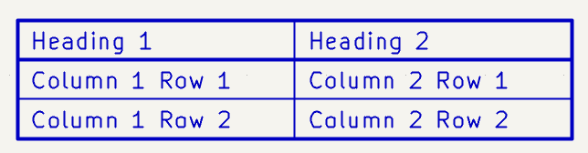
To place a table, use the ![]() button in the right toolbar. Click in the canvas to place the top left corner of the table, then click again to place the bottom right corner of the table and finish drawing the table. The bigger you draw the table, the more rows and columns will be added by default, but rows and columns can be added or deleted after the table is created.
button in the right toolbar. Click in the canvas to place the top left corner of the table, then click again to place the bottom right corner of the table and finish drawing the table. The bigger you draw the table, the more rows and columns will be added by default, but rows and columns can be added or deleted after the table is created.
Once you have created a table, you can edit the table as a whole or edit cells individually. Creating a new table automatically opens the Table Properties dialog to edit the entire table.
You can export a table from KiCad into a CSV file by right clicking a table or table cell and clicking Export Table to CSV….
Editing a whole table
You can edit an entire table with the Table Properties dialog. There are several ways to open the Table Properties dialog:
-
Create a new table. The Table Properties dialog opens automatically when the table is created.
-
Select any cell in the table, right click, and select Edit Table (Ctrl + E).
-
Select the entire table, right click, and select Properties… (E). You can select the entire table with a drag selection or by selecting a single cell, then right clicking and selecting Select Table.
-
Click the Edit Table… button in the Table Cell Properties dialog.
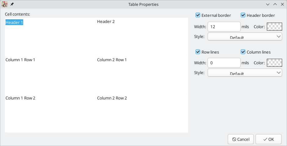
This dialog lets you edit the properties of the entire table, including the text in each cell and the separators between cells. To change the formatting of text in a cell, edit the properties of individual cells, instead of the properties for the entire table.
| The properties for a table can also be edited in the Properties Manager when the entire table is selected. |
The left side of the dialog displays an editable grid of the entire table. You can edit the contents of any cell by clicking on the cell in the grid. You can also edit the text in a cell by selecting the cell and using the Properties Manager. If you have tabular content in a spreadsheet or other table, you can copy and paste that content into the grid here.
| Text in table cells supports the markup described in the text markup section (superscripts, subscripts, strikethroughs, etc.). |
The right side of the dialog contains formatting options for the table.
-
The Locked checkbox controls whether or not the table is locked. Locked objects may not be manipulated or moved, and cannot be selected unless the Locked Items option is enabled in the Selection Filter panel.
-
The External border and Header border checkboxes control whether there is a border drawn around the entire table and the cells in the top row, respectively. When Header border is enabled, the border below the cells in the top row is styled using these external border settings rather than the row/column line settings. The line width of the header borders is controlled by the Width field. When set to 0, the line width uses the default symbol line width configured in the Formatting panel of Schematic Setup. The line color is controlled by the Color picker, and the line style can be set to solid, dashed, dotted, dash-dot, or dash-dot-dot using the Style dropdown menu.
-
The Row Lines and Column lines checkboxes enable horizontal lines between rows and vertical lines between columns, respectively. These have the same formatting options as the external and header borders.
Editing individual table cells
Instead of editing the properties of an entire table, you can also edit the properties of individual cells. This modifies selected cells, but does not affect other cells. To open the Table Cell Properties dialog, double click on a cell, or select a cell, right click, and choose Properties… (E). If you select multiple cells, the properties dialog will act on all of them at once.
| You can select multiple cells by clicking and dragging. |
| To select all cells in a row or column, select a cell in that row or column, right click, and choose Select Row(s) or Select Column(s). You can select multiple rows or columns in this way by starting with multiple cells selected. |
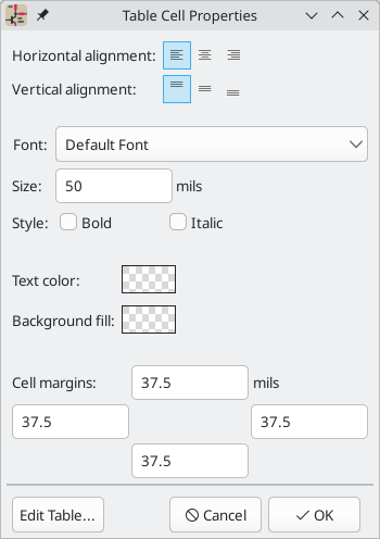
The left side of the dialog lets you edit the contents of the selected cell. The right side of the dialog contains formatting options for the selected cell.
-
Horizontal alignment and Vertical alignment control how text is positioned within the cell.
-
The Font dropdown lets you select a font for the text. You can use any TTF font available on your system, or the built-in KiCad stroke font.
-
Size controls the size of the text in the cell.
-
The Bold and Italic checkboxes bold and italicize the text, respectively. These are three-state checkboxes, which can be set to off, on, or no change. No change is useful when multiple cells with different bold/italic settings are being edited at the same time.
-
The Text color and Background fill color pickers control the color of the text and the cell background, respectively.
-
The Cell margins textboxes control the amount of spacing around the top, bottom, left, and right of the text in the cell.
You can click the Edit Table… button to open the properties dialog for the entire table.
| The properties for a table cell can also be edited in the Properties Manager when one or more table cells is selected. |
Editing table layout
The layout of a table (size and number of columns and rows) is initially set when you create a table, but you can also edit the layout after creation.
To resize a row or column, select a cell in that row or column, then drag the handle on the right (to change the column width) or the bottom (to change the row height) to the desired size.
To add rows or columns, select a cell next to where the new row or column should go, right click, then choose Add Row Above, Add Row Below, Add Column Before, or Add Column After, as desired.
To delete rows or columns, select a cell in the row or column you want to delete, then right click and choose Delete Row(s) or Delete Column(s). To delete multiple rows or columns, start with a selection that spans all the rows or columns you want to delete.
You can merge multiple cells into a single cell by selecting all the cells you want to merge, right clicking, and choosing Merge Cells. To unmerge them, select the merged cell, right click, and choose Unmerge Cells.
Graphic shapes
Graphic rectangles (![]() ), circles (
), circles (![]() ), arcs (
), arcs (![]() ), and lines (
), and lines (![]() ) can all be added using their respective buttons in the right toolbar.
) can all be added using their respective buttons in the right toolbar.

Line width, color, and style (solid, dashed, or dotted) can be configured in the properties dialog for each shape (E). Rectangles, circles, and arcs can also have a fill color set and have their outlines removed.
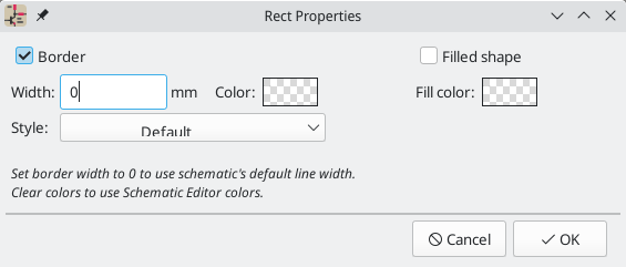
Setting a shape’s line width to 0 uses the schematic default line width, which is configurable in Schematic Setup. Spacing for line dashes is also configurable there. Removing a line or fill color uses the color theme’s graphics color, which is configurable in Preferences.
Like wires, graphic lines obey the line drawing mode setting (90 degree, 45 degree, or free angle), which you can set using the toggle buttons on the left toolbar (![]() ,
, ![]() , and
, and ![]() , respectively). Shift+Space cycles through the modes.
, respectively). Shift+Space cycles through the modes.
As with PCB tracks, the / hotkey switches line posture.
Importing bitmap images
KiCad supports inserting images into the schematic. These are purely for reference during the design process and play no electrical role.
To add a bitmap image, use the ![]() button on the right toolbar and select the desired bitmap image file. Click in the canvas to place the image.
button on the right toolbar and select the desired bitmap image file. Click in the canvas to place the image.
| You can also import a bitmap image by dragging and dropping it onto the editing canvas. |
Once the image has been added to the canvas, you can reposition it using the move tool (M) or by dragging it in the canvas. You can scale it by dragging the editing handles at the corners of the image. The image is scaled around its reference point; in other words, the reference point is the point in the image that always stays in the same position in the canvas, no matter how the image is scaled. The reference point is shown as a fifth editing handle. Initially it is at the center of the image, but you can reposition the reference point by dragging it in the canvas.
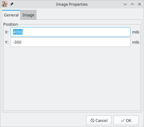
You can also reposition or scale the image in its properties dialog (E). Position and scale in this dialog are relative to the center of the image, not its interactive reference point. You can also Convert to Greyscale if you wish.
Importing vector graphics
You can add graphic shapes from an external vector graphics file by importing the file into KiCad. DXF and SVG files are supported. To import the file, use File → Import → Graphics… (Ctrl+Shift+F).
| You can also import a vector graphics file by dragging and dropping it onto the editing canvas. |
Imported vector graphics are part of the design like any other graphic shape. In other words, they have an assigned board layer, they are included in fabrication outputs, and shapes on copper layers can make electrical connections.
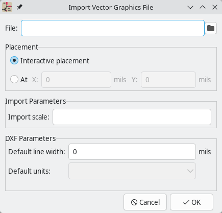
The Import Vector Graphics File dialog has several options:
-
File specifies the vector graphics file to import.
-
If Interactive Placement is selected, you can place the graphics interactively in the canvas after importing. If At is selected, the graphics will instead be placed at the specified coordinates.
-
Import Scale sets the scale factor for the import.
-
DXF default line width sets the line width for any items in a DXF file that do not specify a line width. It has no effect when not importing DXF files.
-
DXF default units sets the default unit for DXF files with unspecified units. It has no effect when not importing DXF files.
Bulk editing text and graphics
Properties of text and graphics, including symbol fields, can be edited in bulk using the Edit Text and Graphic Properties dialog (Edit → Edit Text and Graphic Properties…). The tool can also modify visual properties of wires and buses.
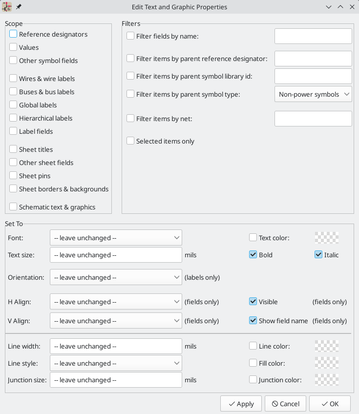
Scope and Filters
Scope settings restrict the tool to editing only certain types of objects. If no scopes are selected, nothing will be edited.
Filters restrict the tool to editing particular objects in the selected scope.
Objects will only be modified if they match all enabled and relevant filters
(some filters do not apply to certain types of objects. For example, symbol
field filters do not apply to wires and are ignored for the purpose of changing
wire properties). If no filters are enabled, all objects in the selected scope
will be modified. For filters with a text box, wildcards are supported: *
matches any number of any characters, including none, and ? matches any single
character.
-
By field name filters to the specified symbol field, label field, or sheet field.
-
By parent reference designator filters to fields in the symbol with the specified reference designator.
-
By parent symbol library id filters to fields in symbols with the specified library identifier.
-
By parent symbol type filters to fields in symbols of the selected type (power or non-power).
-
By net filters to wires and labels on the specified net.
-
Only include selected items filters to the current selection.
Editable Properties
Properties for filtered objects can be set to new values in the bottom part of the dialog.
Drop-down lists and text boxes can be set to -- leave unchanged -- to preserve existing values. Checkboxes can be checked or unchecked to enable or disable a change, but can also be toggled to a third "leave unchanged" state. Color properties must be checked to change the value; a checkerboard swatch indicates that the color will be inherited from the default value from the the schematic settings or net class properties.
Text properties that can be modified are font, text size, text orientation (right/up/leftdown), horizontal and vertical alignment, text color, emphasis (bold and italic), and visibility of fields and field names.
Graphic and wire properties that can be modified are line width, line style (solid, dashed, and dotted lines), line color, fill color for shapes, and junction size and junction color for wire junctions.
Bloque de titulo de la hoja
The drawing sheet’s title block is edited with the Page Settings tool (![]() ). You can also open this tool by double clicking anywhere on any part of the drawing sheet.
). You can also open this tool by double clicking anywhere on any part of the drawing sheet.
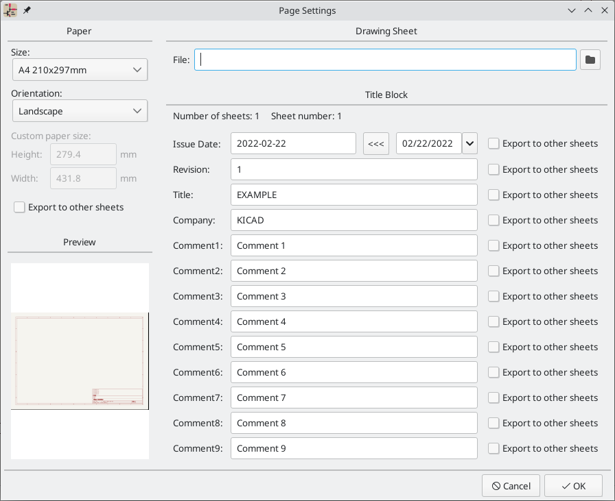
Each field in the title block can be edited, as well as the paper size and orientation. If the Export to other sheets option is checked for a field, that field will be updated in the title block of all sheets, rather than only the current sheet.
You can set the date to today’s or any other date by pressing the left arrow button next to Issue Date. Note that the date listed in the schematic title block is not automatically updated. It is only updated when changed in this dialog.
A drawing sheet file can also be selected to replace the default drawing sheet. When choosing a drawing sheet, you can enable the Embed File checkbox in the file browser to embed the drawing sheet in the schematic instead of referencing an external file. This means the schematic will appear the same when it is opened on another computer that does not have the drawing sheet file available at the same external file path. For more information, see the embedded files documentation.
The sheet number (Sheet X/Y) is automatically updated, but sheet page numbers can also be manually set using Edit → Edit Sheet Page Number….
Groups
Groups let you treat multiple objects as a single object for the purposes of moving or rotating them. Each object in the group will maintain its position relative to the other objects in the group. When objects are grouped, it is difficult to accidentally edit them or move them relative to the other members of the group. Groups can have a name, which is displayed in the editing canvas when the group is selected.
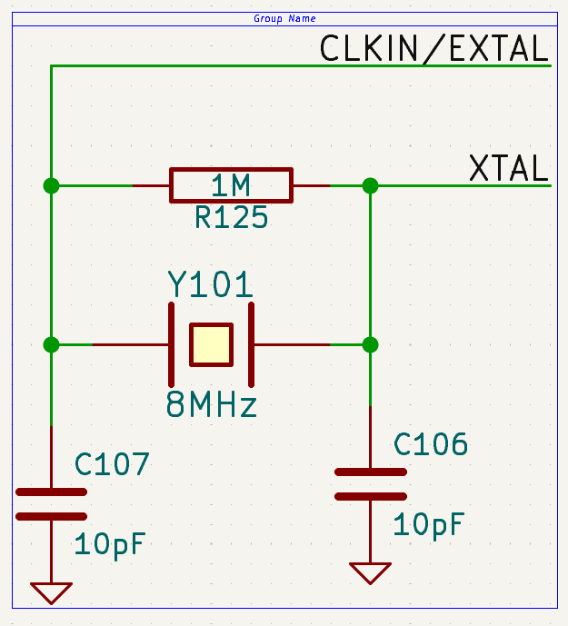
Most types of objects in the Schematic Editor can be grouped: symbols, wires, labels, graphic items, and even other groups. Groups can contain multiple different types of objects at once.
To add objects to a group, select them, then right click and choose Grouping → Group Items, or click the ![]() button in the top toolbar. To remove all items from a group, select the group, right click, and choose Grouping → Ungroup Items, or click the
button in the top toolbar. To remove all items from a group, select the group, right click, and choose Grouping → Ungroup Items, or click the ![]() button in the top toolbar.
button in the top toolbar.
Once objects have been added to a group, selecting any of the objects will select the group as a whole instead of the constituent objects. To edit a specific object within a group, first select the group, the right click and choose Enter Group. Double clicking on a group also enters the group. When a group has been entered, objects within the group can be selected and edited individually without affecting the other objects in the group. To leave the group and stop editing its members individually, right click and select Leave Group, select an object outside the group, or use Esc.
There are several ways to modify which objects belong to a group. To remove objects from an existing group, enter the group, then select the objects you want to remove, right click, and choose Grouping → Remove Items. To add items to a group, first ungroup all the items from the group. This will leave the group’s former members selected. Then add the new item to the selection and group the selection. Note that without first ungrouping, this process would create a nested group: a new group containing the new item and the entire original group, not just the items in the original group.
You can also add or remove objects from a group in the group’s properties dialog. To open a group’s properties dialog, press E or right click and click Properties…. The properties dialog lists the objects contained in the group. To add an additional object to the group, click the ![]() button, then click on the desired object in the editing canvas. The object you click on will be added to the group. To remove an object, select it in the list, then click the
button, then click on the desired object in the editing canvas. The object you click on will be added to the group. To remove an object, select it in the list, then click the ![]() button.
button.
The Library link field is used for design blocks. It specifies the group’s linked design block name and library in the format <library>:<block>. This field must be filled out correctly to link design block schematic groups to the corresponding block in the board and in the design block library.
You can optionally transfer groups from the schematic to the PCB using the Update PCB from Schematic tool. If the Group footprints based on symbol group option is enabled, footprints in the PCB will be grouped if their linked symbols are grouped in the schematic.
Aligning objects
The align tool moves a selection of objects so that they are all aligned with a reference object. There are six different alignments to choose from, depending on which part of the objects you wish to align. Objects can be horizontally aligned by their left, center, or right edges, or they can be vertically aligned by their top, center, or bottom edges. Objects are only moved in one dimension, so objects stay in the same horizontal position when aligned vertically, and vice versa. To align objects by a given edge, select the objects, then right click and choose Align/Distribute → Align to Left (or another alignment as desired).
If the cursor is over an object in the selection, that object is used as the reference object. Otherwise, the reference object is the object in the selection which is located furthest in the alignment direction, for example the leftmost object when aligning by left edge, or the topmost object when aligning by top edge. The topmost object is used when aligning by vertical center, and the leftmost when aligning by horizontal center.
Before alignment
After alignment
In the example above, two circles are vertically aligned by their top edges, with the large circle as the reference object. The first image shows them before alignment and the second image shows them after alignment. In this case, the large circle is the topmost object before alignment, so it is chosen as the reference object if the cursor is not over the other circle. After alignment, the top edges of the circles are at the same position, but the horizontal positions of the circles are unchanged.
| Symbols, labels, and other objects with pin connections are always moved so that their connection points remain on the grid, even if this results in imperfect alignment with the other objects. |
Schematic editing convenience functions
There are several convenience features in the Schematic Editor that make some common editing and connection operations faster.
Pin helpers
You can quickly add wires, labels, or no-connection markers to a selection of pins using the Pin Helpers tools in the right-click context menu. This can help you quickly break out unconnected pins from a symbol or hierarchical sheet. By selecting Pin Helpers → Wire, the wire tool will begin drawing a wire from all selected pins at once. If you select No Connect, no-connection markers will be added to the end of each selected pin. And if you choose Net Label, Hierarchical Label, or Global Label, a label of the respective type will be placed at the end of each selected pin. Each label’s name will be set to the corresponding pin name. The new labels will remain selected, so you can easily move them away from the symbol using M or G, depending on whether you wish to maintain a wired connection between the pins and the labels.
| Pin helpers require you to select individual pins, not their parent symbol or sheet. Symbol pins cannot be individually selected if the clicking on a pin selects the symbol option is enabled in the Editing Options pane of the Schematic Editor preferences. Therefore, this option must be disabled to use the Pin Helper tools. |
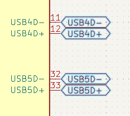
Converting between object types
Existing labels and text objects can be changed to another type of label or text by right clicking the object(s) and selecting the target object type from the Change To submenu. The allowed types for source and target objects are local labels, global labels, hierarchical labels, directive labels, text objects, and text boxes. The value of the original object is preserved in the resulting object: when a text object is converted to a label, the label’s value (net name) will be the original text, and vice versa.
Swapping objects
You can swap the position of two selected objects using the Swap command (Alt+S; also available in the right-click context menu). This works on many schematic items, including symbols, symbol fields, labels, graphical items, and text. The first object is assigned the location and rotation of the second object, and vice versa. If there are more than two objects selected, the locations are cycled: the last object gets the position of the first object, the first object gets the location of the second, and so on.
| One possible use of the swap command is to exchange two units within a symbol, for example the two amplifiers in a dual op-amp. You could also use swap with a selection of labels to modify net assignments to symbol pins. These tasks, and other related operations, can be quickly accomplished using the pin swap and gate swap functions, which work similarly to the generic swap command but are focused on swapping labels, pins, and gates. |
Swapping pins and pin labels
Pin swapping exchanges the assigned nets between a selection of symbol pins, so that the net that was assigned to one pin is moved to a different pin, and vice versa. For example, this could be used to swap the connections between two GPIO pins on a microcontroller. The pins must be part of the same symbol, but otherwise there are no restrictions on which pins can be used in a pin swap.
Pin swaps are unconstrained, which means that KiCad allows you to swap any pins. The tool does not check that the swapped pins are equivalent.
| It is up to you to ensure that the new pin connections are valid after a pin swap. |
There are two forms of pin swapping in the Schematic Editor.
-
Swap the labels connected to each pin by selecting the pins, right clicking, and choosing Swap Pin Labels.
-
Swap the pins, leaving the connected wires/labels in the same place but changing the locations of the pins themselves, by selecting the pins, right clicking, and choosing Swap Pins. This modifies the pin locations in the symbol itself (this modifies the schematic’s copy of the symbol but does not affect the library symbol).
Because the Swap Pins tool modifies symbols in the schematic, it is not available unless the Allow unconstrained pin swaps option is enabled in the Editing Options page of the Schematic Editor preferences. If this option is not enabled, pin labels can be swapped, but pins themselves cannot.
Both forms of pin swapping result in the nets being exchanged between the selected pins. If there are more than two objects selected, the locations are cycled: the last object gets the position of the first object, the first object gets the location of the second, and so on.
Gate (unit) swaps
Gate swaps exchange the connections between two or more units ("gates") of the same multi-unit symbol. All of the nets attached to one symbol unit’s pins are exchanged with the corresponding nets from another unit of the same symbol. For example, this could be used to swap between two opamp units in the same package, or two resistors in a resistor array. In this context, gate refers to to a symbol unit.
Gate swaps are unconstrained, which means that KiCad allows you to swap any units. The tool does not check that the swapped units are equivalent.
You can perform gate swaps in two ways.
-
Swap the units themselves by selecting the units, right clicking, and choosing Swap (Alt+S). In this case, the symbol units exchange places, but the surrounding connections are not changed. Use this option when you don’t want to disturb the schematic connections surrounding each symbol unit.
Swapping units in this way is equivalent to manually changing the unit for each unit you wish to swap. Another fast way to swap symbol units is to right click a single unit and choose another unit from the Symbol Unit submenu. If the new unit was already placed, KiCad will give you the option to swap the units. -
Swap the labels on each unit, while keeping the symbol units themselves in the same place, by selecting the units, right clicking, and choosing Swap Unit Labels. This can only be used when each pin of the symbol unit is connected to a single net label and nothing else. If the schematic connections to the pins are not merely net labels, use the other option instead. This function can also only be used on units that are part of the same symbol and have the same number of pins.
Schematic Setup
The Schematic Setup window is used to set schematic options that are specific to the currently active schematic. For example, the Schematic Setup window contains formatting options, electrical rule configuration, net class setup, and schematic text variable setup.
To open Schematic Setup, use File → Schematic Setup… or press the ![]() button in the top toolbar.
button in the top toolbar.
Schematic formatting
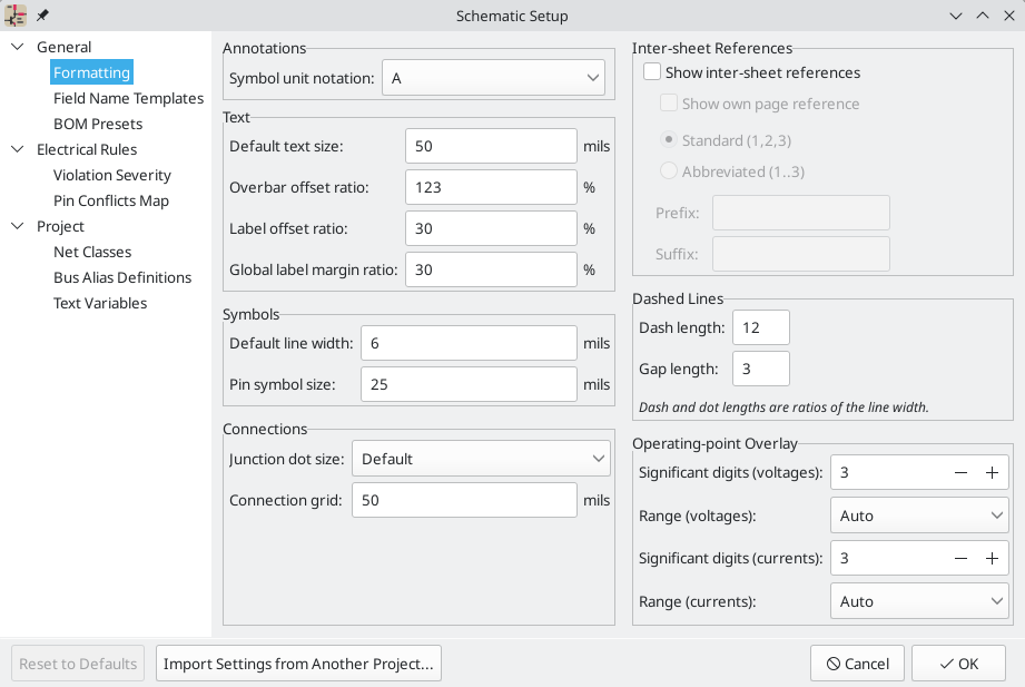
The formatting panel contains settings for the appearance of symbols, text, labels, graphics, and wires.
Symbol unit notation sets how each unit of a multi-unit symbol is referred to
in its reference designator. By default, a different letter for each unit is
appended to the reference designator with no separator, for example U1B for
the second unit of symbol U1, but this can be changed. Numbers can be used
instead of letters, and various separators can be used between the symbol
designator and the unit identifier (., -, _, or none).
Default text size sets the default text height used by the text, text box, and
label tools. Overbar offset ratio controls the vertical spacing between text
and an overbar (~{}) over that text, as a ratio of the text height.
Label offset ratio controls the vertical spacing between a local label’s text
and the attached wire, relative to the label’s text size. This also affects the
spacing between symbol pins and their pin number. Global label margin ratio
defines the size of the box around a global label, relative to the global
label’s text size. Increasing the margin may be useful to avoid overlapping text
with overbars (~{}) or letters with descenders, but this may cause closely
packed global labels to overlap with each other.
Default line width sets the default line width for symbol graphics, if the symbol does not override the default line width. Pin symbol size scales symbol pin graphic style annotations, such as the bubble on an inverted pin.
Hop-over size sets the size of wire hop-overs, which are optionally drawn when one wire crosses another wire without connecting. By default the size is set to None, which means hop-overs are not drawn.
Junction dot size sets the schematic’s default wire junction dot size. The default size can be overridden by editing an individual junction dot’s properties. Connection width specifies the grid size used for the Symbol pin or wire end off connection grid ERC check. Schematics typically use a 50 mil grid for electrical connections, so this should usually remain set at 50 mils.
The Operating Point Overlay settings configure how operating point simulation annotations are displayed on the schematic canvas. The significant digits settings control the number of significant digits printed on voltage and current overlays. The range settings control the units used to display voltage and current measurements.
Show inter-sheet references enables or disables the display of
inter-sheet references, which are a list of page
numbers next to a global labels that link to other places in the schematic where
the same global label appears. Show own page reference controls whether the
current page is included in the list of page numbers. Standard and
abbreviated determine whether to display the complete list of page numbers or
only the first and last page numbers. The prefix and suffix fields add
optional characters before and after the list of page numbers. In the image
of an inter-sheet reference below, a prefix and suffix of [ and ],
respectively, have been added.
Dashed line appearance is controlled in the Formatting section. Dash length controls the length of dashes, while Gap length controls the spacing between dashes and dots. The dash and gap lengths are relative to the line width: a gap length of 2 means twice the width of the line.
Annotation options
The Annotation panel contains settings for how symbols are annotated.
Symbol unit notation sets how each unit of a multi-unit symbol is referred to
in its reference designator. By default, a different letter for each unit is
appended to the reference designator with no separator, for example U1B for
the second unit of symbol U1, but this can be changed. Numbers can be used
instead of letters, and various separators can be used between the symbol
designator and the unit identifier (., -, _, or none).
The Order and Numbering sections control how symbols are automatically annotated.
-
When multiple symbols are added simultaneously, they are annotated according to the Order setting, sorted by either X or Y position.
-
The Numbering option sets the starting number for new reference designators. This can be the lowest available number, or a number based on the sheet number. When Allow reference reuse is enabled, reference designators can be automatically assigned as long as they are not currently used by another symbol. When disabled, a reference designator can never be used again once it has been assigned to a symbol, even if it is not currently in use.
Field name templates
Field name templates are empty symbol fields that are automatically added to all symbols in the schematic. These can be useful when every symbol in the schematic needs additional fields beyond the fields that are defined in the library symbols, for example a field for the manufacturer’s part number.
Template fields can be set as visible or invisible, and can also be set as URL fields.
Field name templates that are defined in schematic setup apply only to the current project. Field name templates can also be defined in Preferences, which apply to all projects edited on your computer.
BOM presets
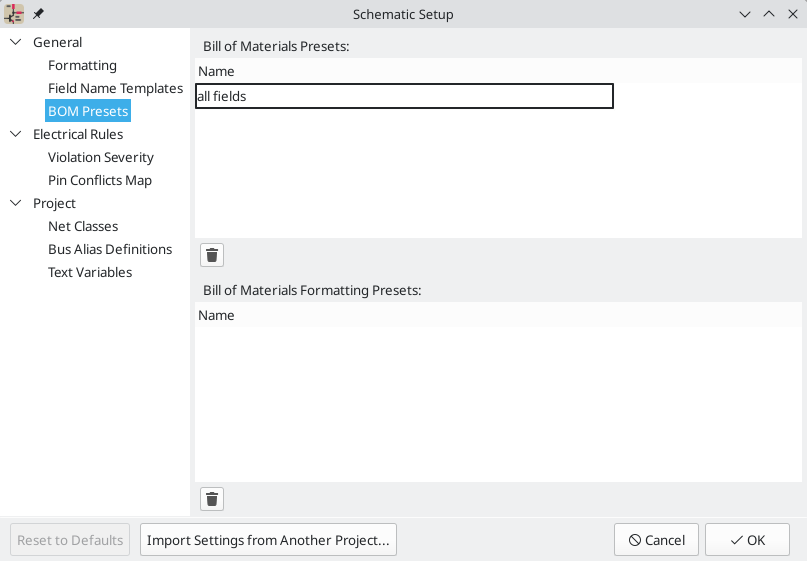
BOM presets are saved configurations for the Symbol Fields Table and BOM export tool. There are two types of presets. BOM presets configure which fields are displayed in the symbol fields table, which order they are displayed in, and how they are used to group symbols. These fields are also directly used in the BOM output. BOM formatting presets configure the output BOM file format, including which separator characters are used to separate fields. Both types of presets are created in the Symbol Fields Table, but can are listed and can be deleted here.
ERC violation severity and pin conflicts map
The Violation Severity panel lets you configure what types of ERC messages should be reported as Errors, Warnings, or ignored.
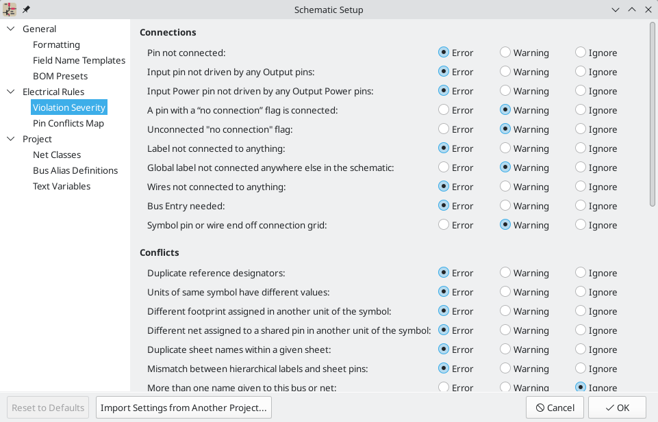
The Pin Conflicts Map allows you to configure connectivity rules to define electrical conditions for errors and warnings based on what types of pins are connected to each other. For example, by default an error is produced when an output pin is connected to another output pin.
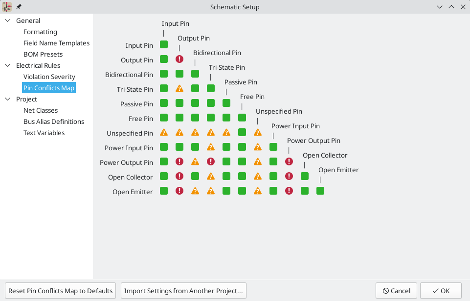
These panels are explained in more detail in the ERC section.
Net classes
The Net Classes panel allows you to manage net classes for the project and assign nets to net classes with patterns. Managing net classes in this panel is equivalent to managing them in the Board Setup dialog. Nets can also be assigned to net classes in the schematic using graphical assignments with net class directives or net labels.
Pattern-based net class assigment is explained in more detail in the net classes section.
Bus alias definitions
The Bus Alias Definitions panel allows you to create bus aliases, which are names for groups of signals in a bus. For more information about bus aliases, see the bus alias documentation.
Text variables
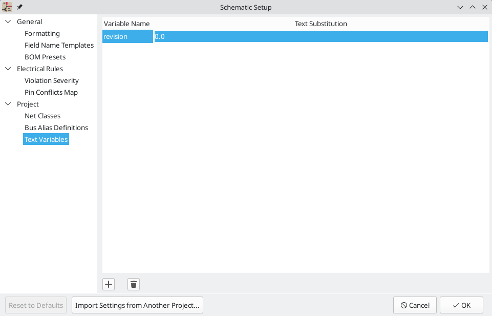
Text variables can be created in the Text Variables section. KiCad will substitute the variable name with the text string assigned to the variable. This substitution happens anywhere the variable name is used inside the variable replacement syntax of ${VARIABLENAME}.
For example, you could create a variable named VERSION and set the text substitution to 1.0. Now, in any text object in the schematic, you can enter ${VERSION} and KiCad will display this as 1.0. If you change the value to 2.0, every text object that includes ${VERSION} will be updated automatically. You can also mix regular text and variables. For example, you can create a text object with the text Version: ${VERSION} which will be displayed as Version: 1.0.
Text variables can also be created in Board Setup. Text variables are project-wide; variables created in the schematic editor are also available in the board editor, and vice versa.
There are also a number of built-in system text variables.
Embedding files
External files can be embedded within a schematic. Embedding a file stores a copy of the file inside the schematic file. The design can then refer to the embedded copy of the file instead of the external file, which makes the project more portable as it doesn’t rely on an external file. Fonts, datasheets, drawing sheets, SPICE models, and footprint 3D models can be embedded and used within KiCad. Other arbitrary files can also be embedded to store them in the project for later export, but they are not used by any KiCad functionality. Files embedded in a schematic necessarily increase the schematic’s file size, although files are compressed before being embedded to minimize the space required.
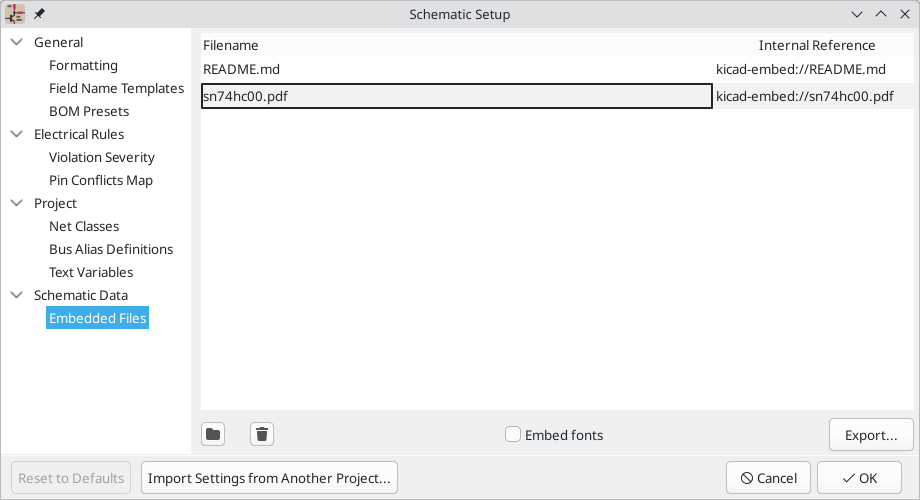
Embedded files are managed in the Embedded Files section of Schematic Setup. All files embedded in a schematic are shown here. To embed a file inside a schematic, click the ![]() button and select the file. The file is then embedded inside the schematic and is listed in the embedded files list along with its embedded reference. The embedded reference is a unique identifier for the embedded file that begins with
button and select the file. The file is then embedded inside the schematic and is listed in the embedded files list along with its embedded reference. The embedded reference is a unique identifier for the embedded file that begins with kicad-embed://. You can use the embedded reference elsewhere in the Schematic Editor to refer to the embedded file as if it were an external file path. You can copy the embedded reference by right clicking and selecting Copy Embedded Reference. To remove an embedded file, click the ![]() button. Any remaining links to the removed file will become invalid.
button. Any remaining links to the removed file will become invalid.
| Datasheets, SPICE models, and drawing sheets can be embedded directly using the file browser when you add them to a symbol (datasheets and SPICE models) or to a schematic (drawing sheets) by enabling the Embed Files option in the file browser. This is a single-step shortcut for adding the files in Schematic Setup and then referring to them by their embedded reference; the result is the same. |
To embed any fonts used in a schematic, check the Embed fonts checkbox. All fonts used in the schematic will be embedded, so text using that font can be edited on any computer regardless of whether the font file is installed.
You can also embed files in a symbol. Such files will be available within the symbol, but not within the larger schematic or in other symbols. Files embedded in a symbol are deduplicated when the symbol is added to a schematic: if a file is embedded in a symbol, and multiple instances of that symbol are added to the schematic, only one copy of the file will be embedded, and all of the symbol instances will refer to the same embedded file.
As an example, to embed a datasheet in a project and use it within several symbols, you could embed the datasheet using the schematic setup dialog, copy the internal reference, and paste the internal reference into the datasheet field of each symbol that uses that datasheet. Each symbol would then have a portable reference to the embedded datasheet. Alternatively, you could embed the datasheet within the library symbol. In this case, each symbol will already have the datasheet embedded when the symbol is added to a schematic. A more convenient way to achieve the same thing, however, is to open the symbol’s properties dialog, browse for a datasheet file, and enable the Embed File option in the file browser. Again, this could be done for a symbol in the schematic or for a symbol in the source symbol library.
Files can also be embedded in boards.
Importing settings
You can import some or all of the schematic setup from an existing schematic. This allows you to choose a schematic to use as a template and select which settings to import.
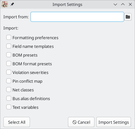
To import settings, click the Import Settings from Another Project… button at the bottom of the Schematic Setup dialog and then choose the .kicad_sch file you want to import from. Select which settings you want to import and the current settings will be overwritten with the values from the chosen schematic.
The settings that are available to import are:
-
Formatting preferences
-
Annotation preferences
-
Field name templates
-
BOM presets
-
BOM format presets
-
Violation severities
-
Pin conflict map
-
Net classes
-
Bus alias definitions
-
Text variables
Opening legacy schematics
Modern versions of KiCad can always open projects created in older versions of KiCad. However, schematics created in some older versions of KiCad have special considerations that must be observed when opening them in order to prevent any data loss.
Opening KiCad 5.0 and 5.1 schematics
Modern versions of KiCad can open schematics created in versions prior to KiCad 6.0, but the cache library file (<projectname>-cache.lib) must be present to load the schematic correctly.
Since version 6.0, KiCad stores all symbols used in a project in the schematic. This means that you can open a schematic made in KiCad 6.0 or later on any computer, even if the libraries used in the project are not installed or have changed. Modern KiCad schematic files use the .kicad_sch extension.
Prior to version 6.0, KiCad did not store symbols in the schematic. Instead, KiCad stored references to the symbols and their libraries. It also stored a copy of every symbol used by the project in a separate cache library file (<projectname>-cache.lib). As long as the cache library was included with the project, the project could be distributed without the system library files, because KiCad could load any needed symbols from the cache library as a fallback if the libraries referenced in the schematic were missing. Legacy KiCad schematic files use the .sch extension.
When you open a legacy schematic, KiCad will look in the cache library to find all of the symbols used in the schematic in the cache library. When you save the legacy schematic, KiCad will save it as a new file in the modern schematic format (.kicad_sch), with the necessary symbols embedded in the schematic itself. The original legacy schematic and the cache library will remain, unmodified, but they are no longer necessary once the schematic has been saved in the modern format.
| Projects created in KiCad prior to version 6.0 must have a cache library. If the cache library is missing, the schematic will lose symbol information if the system symbol libraries are modified, reorganized, moved, or deleted. The libraries included with legacy versions of KiCad are substantially different than the modern KiCad libraries, so in practice KiCad will almost always fail to open legacy projects unless the cache library is present. |
When you open a legacy schematic, KiCad may display the Project Rescue Helper dialog. This means that one or more symbols in the cache library do not match the corresponding symbol in the external library. The dialog helps you "rescue" symbols from the cache library into your schematic, if desired. You can also open the rescue dialog at any time using Tools → Rescue Symbols…. The cache library file must be present in order to use the rescue tool.
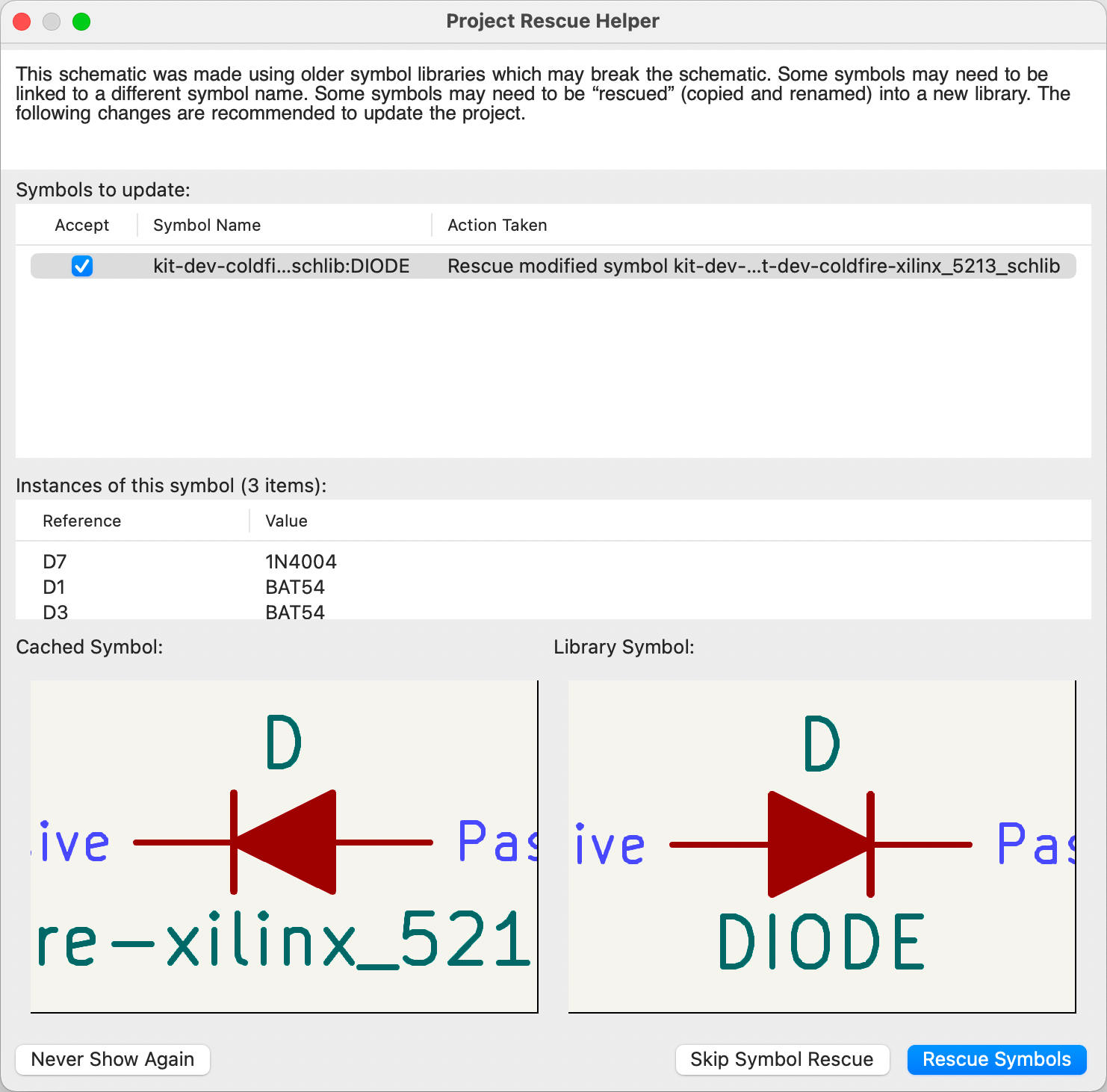
The rescue dialog lists all symbols that don’t match between the cache library and the external symbol library. The discrepancy can be because:
-
the cached symbol or the library symbol has been modified, so the two symbols no longer match, or
-
the cached symbol does not have a corresponding symbol in the symbol library, because the symbol or library was moved, renamed, deleted, or is not present on the current computer.
For each symbol in the list, selecting the symbol displays the reference designator and value for each instance of the symbol, and shows a visual preview of the symbol. If a corresponding symbol exists in the system symbol library, the dialog shows both copies of the symbol for comparison. If the symbol only exists in the cache library, the dialog only shows the cached symbol.
In this example, the project originally used a diode with the cathode facing left, but the library now contains one with the cathode facing right. This change would break the design, so it would be important to use the cached symbol as the original designer intended.
Pressing Rescue Symbols here will cause the selected symbols from the cache library to be saved into a special rescue library (<projectname>-rescue.kicad_sym). The corresponding symbols in the schematic will be updated to use the newly rescued symbols. Any unselected symbols will not be rescued, but their symbol linkage can be updated in the schematic later.
Alternatively, pressing Skip Symbol Rescue will exit the dialog without rescuing any symbols. KiCad will use the versions of the symbols found in the external libraries. You can run the rescue function again with Tools → Rescue Symbols…, or manually edit symbol linkage in the symbol’s properties.
If you would prefer not to see this dialog, you can press Never Show Again. This has the same effect as pressing Skip Symbol Rescue for the current schematic and all future schematics.
If a symbol in a legacy schematic cannot be found in either the cache library or the external library, KiCad cannot rescue that symbol. A placeholder symbol is inserted into the schematic in its place, as shown below.
You can attempt to remap these orphaned symbols using the Change Symbols or Edit Symbol Library Links dialogs, but either option may require manual corrections to the schematic. These tools are explained in more detail in the Updating and exchanging symbols section.
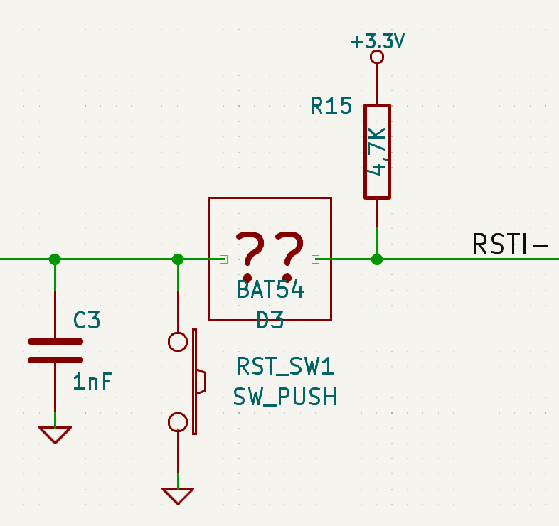
Opening pre-5.0 schematics
Modern versions of KiCad can open schematics created in versions prior to KiCad 5.0, but you will need to go through a symbol remapping process to open the schematic without losing symbol information.
Since version 5.0, KiCad schematics refer to specific symbols using both the symbol and library name. Even if multiple libraries each contain a symbol with the same name, the designer’s intended symbol is unambiguously specified.
Prior to version 5.0, KiCad schematics stored only the symbol name, not the library name. Symbols in the schematic were indirectly mapped back to the original library by searching through the project’s library list for a matching symbol. When you open a pre-5.0 schematic, KiCad will attempt to automatically "remap" the symbols so that each bare symbol name is replaced with a fully-specified symbol library and symbol name pair. The original schematics will be backed up in a rescue-backup folder.
You can skip the automatic remapping, but you will need to remap the symbols yourself using the Change Symbols dialog. You can also re-run the Remap Symbols tool using Tools → Remap Legacy Library Symbols….
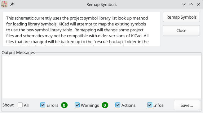
Multiple sheets and hierarchical schematics
Schematics can contain multiple sheets, which can be arranged and connected to each other in several ways. Schematic sheets are organized in a hierarchy, with some sheets organized at the top level of the hierarchy ("top-level sheets"), and others organized as subsheets of top-level sheets or other subsheets ("hierarchical sheets"). Hierarchical sheets are drawn inside another sheet and are organized under that sheet in the schematic hierarchy. Hierarchical sheets can be included in a hierarchy multiple times, if desired.
| Before KiCad 10.0, all multi-sheet schematics in KiCad were hierarchical. Schematics could only have a single top-level sheet, and all other sheets were created as subsheets of the root sheet or other subsheets. Beginning in KiCad 10.0, schematics can have multiple top-level sheets. |
Creating a multi-sheet schematic starts from the first sheet. The process is to create a new sheet, either as a top-level sheet or a hierarchical sheet, then draw the circuit in the subsheet and make the necessary electrical connections between sheets. Connections can be made between nets in different sheets using global labels. For hierarchical sheets, you can also make connections from a subsheet to the parent sheet using hierarchical labels and hierarchical sheet pins.
Carefully considering the best way to organize sheets in a schematic, including whether to draw the schematic hierarchically, improves schematic legibility and reduces repetitive drawing.
Adding top-level sheets to a design
The most basic way to add new sheets to a design in KiCad is to add new top-level sheets. This puts new sheets at the same level of the hierarchy as the existing root sheet, creating a flat schematic where sheets are at the same level rather than nested. Unlike hierarchical subsheets, top-level sheets are not subsheets and are not displayed as sheet symbols in another sheet. You cannot make hierarchical connections between top-level sheets; net connections between top-level sheets can only be made using global labels and global power symbols. Each top-level sheet is saved as a separate .kicad_sch file.
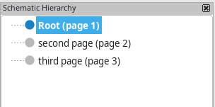
To create a new top-level sheet, right click in the Schematic Hierarchy panel and choose New Top-Level Sheet (if the Schematic Hierarchy panel is not shown, you can show it with View → Panels → Hierarchy Navigator). After choosing a sheet name for the new sheet, the sheet is added to the hierarchy. You can choose a new page number for the sheet by right clicking it in the hierarchy and choosing Edit Page Number or rename the sheet by right clicking and choosing Rename.
Adding hierarchical subsheets to a design
Another way to add additional sheets to a design is using hierarchical subsheets. Subsheets are drawn as a sheet symbol inside of another sheet. The new subsheet is placed beneath the parent sheet in the sheet hierarchy. A net in a sheet can be connected to a subsheet, and vice versa, through a hierarchical sheet pin at the parent sheet level and a matching hierarchical label in the subsheet. Like top-level sheets, each new hierarchical subsheet is saved as a separate .kicad_sch file.
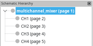
When you add a hierarchical subsheet, you can either create a new sheet or reuse an existing sheet. By reusing an existing sheet, you can use the sheet multiple times in a design. The existing sheet file is used for each instantiation; no new sheet file is created when it is reused. Any edits to the contents of one hierarchical sheet instantiation also affect the other instantiations. The only thing that varies between instantiations of a hierarchical sheet are the reference designators of the symbols in the sheet, which are unique between instantiations.
| Sheet files can be shared between multiple projects to allow design reuse between projects. However, this is not recommended due to path portability concerns and the risk of unintentionally changing other projects while editing a shared sheet. |
You can add a hierarchical subsheet to a design with the Add Hierarchical Sheet tool (S hotkey, or the ![]() button in the right toolbar). Launch the tool, then click twice in the canvas to draw the upper left and lower right corners of the subsheet symbol (you can also click and drag). Make the sheet outline large enough to fit the hierarchical pins you will add later.
button in the right toolbar). Launch the tool, then click twice in the canvas to draw the upper left and lower right corners of the subsheet symbol (you can also click and drag). Make the sheet outline large enough to fit the hierarchical pins you will add later.
The Sheet Properties dialog will appear and prompt you for a sheet name and filename.
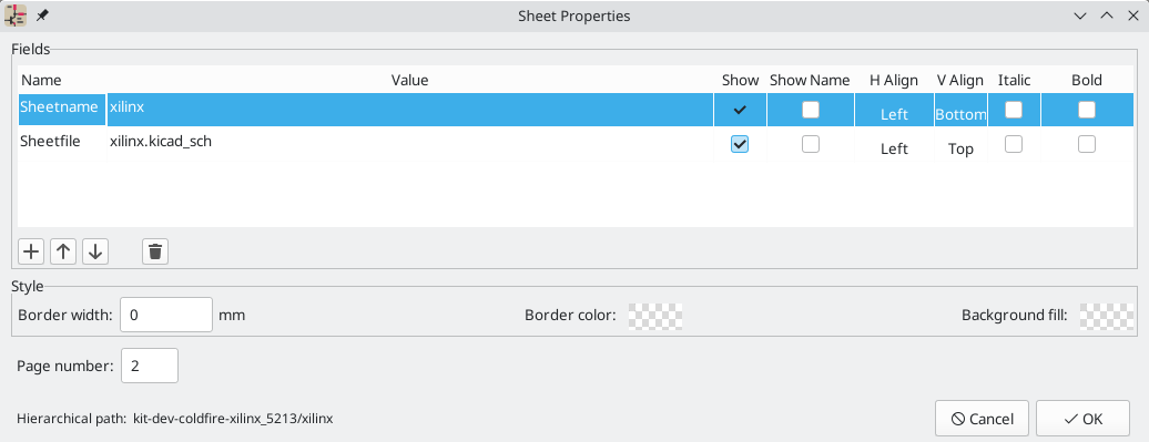
The sheet name must be unique, as it is used in the full net name for any nets in the subsheet. For example, a net with the local label net1 in the sheet sheet1 would have a full net name of /sheet1/net1. The sheet name is also used to refer to the sheet in various places in the GUI, including the title block and the hierarchy navigator. The sheet name can also be changed in the hierarchy navigator.
The sheet file specifies the file that the new sheet will be saved to or loaded from. The path to the sheet file can be relative or absolute. It is usually preferable to save subsheet files in the project directory and use a relative path so that the project is portable.
A single sheet file can be used more than once in a project by specifying the same filename for each repeated sheet; the circuit drawn in the sheet will be instantiated once per usage, and any edits in once instance will be reflected in the other instances.
The sheet’s page number is configurable here. The page number is displayed in the sheet title block and the hierarchy navigator, and sheets are sorted by page number in the hierarchy navigator and when printing or plotting. The sheet number can also be changed in the hierarchy navigator or for the current page with Edit → Edit Sheet Page Number….
Other attributes for sheets are Exclude from simulation, Exclude from bill of materials, Exclude from board, and Do not populate. When any of these attributes are set for a sheet, they are inherited by all symbols in that sheet, as if they were set on the symbols themselves.
Several graphical options are also available. Border width sets the width of the border around the sheet shape. Border color and Background fill set the color for the border and fill of the sheet shape, respectively. If no color is set, a checkerboard swatch is shown and the default values from the color theme are used.
Sheets support arbitrary custom fields, which can be added and removed with the ![]() and
and ![]() buttons, respectively. Sheet fields can be optionally displayed on the schematic by checking their Show box, and they can be accessed from inside the sheet or in other sheet fields using text variables.
buttons, respectively. Sheet fields can be optionally displayed on the schematic by checking their Show box, and they can be accessed from inside the sheet or in other sheet fields using text variables.
The Sheet Properties dialog can be accessed at any time by selecting a sheet symbol and using the E hotkey, or by right-clicking on a sheet symbol and selecting Properties….
Once a new sheet has been added, you can open it to draw a circuit in it as you would in any other schematic sheet.
| You can also drag and drop a selection of existing circuit elements onto the child sheet symbol, which moves the selection into the child sheet. |
Navigating between sheets
You can enter a hierarchical sheet from the parent sheet by double-clicking the child sheet’s shape, or right-clicking the child sheet and selecting Enter Sheet.
Return to the parent sheet by using the ![]() button in the top toolbar, or by right-clicking in an empty part of the schematic and clicking Leave Sheet.
button in the top toolbar, or by right-clicking in an empty part of the schematic and clicking Leave Sheet.
You can jump to the next sheet with the ![]() button, or to the previous sheet with the
button, or to the previous sheet with the ![]() button.
button.
Alternatively, you can jump to any sheet with the hierarchy navigator. To open the hierarchy navigator, click the ![]() button in the left toolbar. The hierarchy navigator docks at the left of the screen. Each sheet in the design is displayed as an item in the tree. Clicking a sheet name opens that sheet in the editing canvas. You can also use the hierarchy navigator to rename or renumber a sheet by right clicking on the sheet name and selecting Edit page number or Rename.
button in the left toolbar. The hierarchy navigator docks at the left of the screen. Each sheet in the design is displayed as an item in the tree. Clicking a sheet name opens that sheet in the editing canvas. You can also use the hierarchy navigator to rename or renumber a sheet by right clicking on the sheet name and selecting Edit page number or Rename.
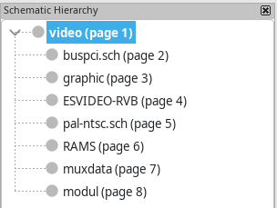
Electrical connections between sheets
Electrical connections between sheets are made with labels. There are several kinds of labels in KiCad, each with a different connection scope.
-
Local labels only make connections within a sheet. Therefore local labels cannot be used to connect between sheets. Local labels are added with the
button. -
Global labels make connections anywhere in a schematic, regardless of sheet. Therefore global labels can be used to make connections between sheets whether the sheets are top-level or hierarchical. Global labels are added with the
button. -
Hierarchical labels in a hierarchical subsheet connect to hierarchical sheet pins accessible in the parent sheet. Hierarchical designs rely on hierarchical labels and pins to make connections between parent sheets and child sheets. You can think of sheet pins as defining the interface for a subsheet; hierarchical labels within the child sheet connect to corresponding sheet pins which are visible in the parent sheet. Hierarchical labels are added inside a child sheet using the
button.
| Labels that have the same name will connect, regardless of the label type, if they are in the same sheet. |
| Hidden power pins can also be considered global labels, because they connect anywhere in the schematic hierarchy. |
Hierarchical sheet pins
After placing hierarchical labels within a subsheet, matching hierarchical sheet pins can be added to the subsheet symbol in the parent sheet. You can then make connections to the hierarchical pins with wires, labels, and buses. Hierarchical sheet pins in a subsheet symbol are connected to the matching hierarchical labels in the subsheet itself.
| Hierarchical labels must be defined in the subsheet before the corresponding hierarchical sheet pin can be imported in the sheet symbol. |
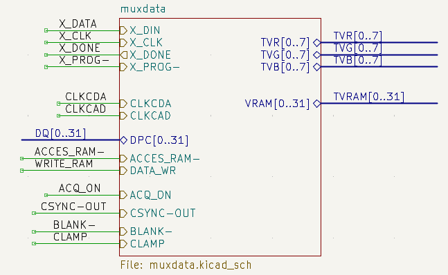
For every hierarchical label in the subsheet, add the corresponding hierarchical pin onto the sheet symbol by clicking the ![]() button in the right toolbar, then clicking on the sheet symbol. A sheet pin for the first unmatched hierarchical label will be attached to the cursor, where it can be placed anywhere along the border of the sheet symbol. Clicking again with the tool will continue to add additional sheet pins until all of the hierarchical labels in the subsheet have a matching sheet pin on the sheet symbol. Sheet pins can also be imported by selecting Place Sheet Pin in a sheet symbol’s right-click context menu.
button in the right toolbar, then clicking on the sheet symbol. A sheet pin for the first unmatched hierarchical label will be attached to the cursor, where it can be placed anywhere along the border of the sheet symbol. Clicking again with the tool will continue to add additional sheet pins until all of the hierarchical labels in the subsheet have a matching sheet pin on the sheet symbol. Sheet pins can also be imported by selecting Place Sheet Pin in a sheet symbol’s right-click context menu.
You can edit the properties of a sheet pin in the Sheet Pin Properties dialog. Open this dialog by double-clicking a sheet pin, selecting a sheet pin and using the E hotkey, or right-clicking a sheet pin and selecting Properties….
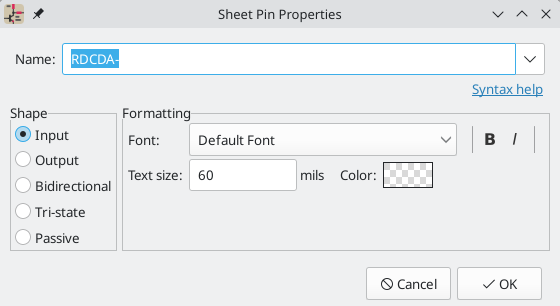
The sheet pin’s name can be edited in the textbox or by selecting from the dropdown list of hierarchical labels in the subsheet. A sheet pin’s name has to match the corresponding hierarchical label in the subsheet, so if you change a pin name you must change the label name as well.
Shape changes the shape of the sheet pin, and has no electrical effect. It can be set to Input, Output, Bidirectional, Tri-state, or Passive. The pin’s font, text size, color, and emphasis (bold or italic) can also be changed.
Syncing sheet pins
Another way to manage the connections between hierarchical labels and sheet pins is to use the Sync Sheet Pins tool. Launch this tool using the ![]() button in the right toolbar or with Sync Sheet Pins in a sheet symbol’s right click context menu.
button in the right toolbar or with Sync Sheet Pins in a sheet symbol’s right click context menu.
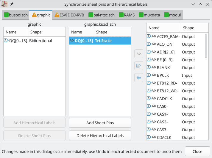
This dialog shows the hierarchical labels and hierarchical sheet pins for each hierarchical sheet. If the tool was launched from the context menu of a sheet symbol, only one tab will be available, with the labels and sheet pins for that specific sheet. If the tool was started globally, i.e. with the ![]() button or with Place → Sync Sheet Pins, a tab will be shown for each hierarchical sheet. If a sheet was selected in the editing canvas when the tool was launched, the dialog will open to that sheet’s tab.
button or with Place → Sync Sheet Pins, a tab will be shown for each hierarchical sheet. If a sheet was selected in the editing canvas when the tool was launched, the dialog will open to that sheet’s tab.
The icon in each tab indicates whether the hierarchical sheet pins on the sheet symbol are correctly matched with the hierarchical labels inside the sheet. If the tab has a ![]() icon, then there is a hierarchical label in the sheet without a matching sheet pin, or a sheet pin without a corresponding hierarchical label, or both. If the tab has a
icon, then there is a hierarchical label in the sheet without a matching sheet pin, or a sheet pin without a corresponding hierarchical label, or both. If the tab has a ![]() icon, then the hierarchical labels and hierarchical sheet pins are matched up correctly. Sheet pins and labels are considered matching if they have the same name and the same graphic shape (input, output, bidirectional, tri-state, or passive).
icon, then the hierarchical labels and hierarchical sheet pins are matched up correctly. Sheet pins and labels are considered matching if they have the same name and the same graphic shape (input, output, bidirectional, tri-state, or passive).
The column on the left lists sheet pins for the current sheet that do not have a corresponding hierarchical label in the sheet. The middle column lists hierarchical labels in the current sheet that do not have a corresponding hierarchical sheet pin on the sheet symbol. The right column lists pairs of matching sheet pins and hierarchical labels. The name of each pin or label is shown along with its graphic shape.
If you click the Add Hierarchical Labels button, new hierarchical labels corresponding to the selected sheet pins will be created for you to place sequentially in the sheet. The selected sheet pins are then removed from the left column and added to to the right column for matching sheet pins and labels. Clicking Delete Sheet Pins will delete the selected sheet pins from the sheet symbol.
If you click the Add Sheet Pins button, new sheet pins corresponding to the selected hierarchical labels will be created for you to place on the sheet symbol. The hierarchical labels are then removed from the middle column and added to the right column for matching sheet pins and labels. Clicking Delete Hierarchical Labels will delete the selected hierarchical labels from inside the sheet.
Clicking the ![]() button will match the selected sheet pin and hierarchical label by renaming the sheet pin to match the hierarchical label’s name. Clicking the
button will match the selected sheet pin and hierarchical label by renaming the sheet pin to match the hierarchical label’s name. Clicking the ![]() button will do the opposite, matching the selected sheet pin and hierarchical label by renaming the label to match the sheet pin.
button will do the opposite, matching the selected sheet pin and hierarchical label by renaming the label to match the sheet pin.
Clicking the ![]() button will unmatch a matched pair, moving both the sheet pin and the hierarchical label back to their respective unmatched columns. The unmatched sheet pin and hierarchical label can then be edited or rematched as desired.
button will unmatch a matched pair, moving both the sheet pin and the hierarchical label back to their respective unmatched columns. The unmatched sheet pin and hierarchical label can then be edited or rematched as desired.
Any changes made in the Sync Sheet Pins dialog are applied immediately, before the dialog is closed. To cancel a change made in the Sync Sheet Pins dialog, use Undo.
Multipage and hierarchical design examples
Multipage schematics in KiCad can be arranged in several ways. Which schematic organization is most appropriate depends on the design.
A design that conceptually contains nested blocks lends itself well to a hierarchical organization, especially if some of the blocks are repeated, because each block can be represented as a hierarchical subsheet. On the other hand, designs that conceptually don’t contain a hierarchy might be better represented using top-level sheets. You can also both strategies in the same schematic, using multiple top-level sheets while also using hierarchical subsheets.
Some examples of different schematic organizations are shown below.
Flat schematics
Flat schematics contain multiple top-level sheets; each top-level sheet follows the previous sheet, and all top-level sheets are at the same level of the hierarchy. None of the top-level sheets are nested under another sheet.
In the example below there are three top-level sheets, each with a name and a page number. They are not hierarchically nested, so hierarchical connections with hierarchical labels and sheet pins are impossible. Any net connections between sheets must be made with global labels (and global power symbols).
Esquemas Jerarquicos
An example of a hierarchical design is the video demo project included with KiCad. The root sheet contains seven unique subsheets, each with hierarchical labels and sheet pins linking the sheets to each other in the root sheet. Each of the seven subsheets is used once; none are reused (see the next section for an example of reusing subsheets). Two of the subsheet symbols are shown below.
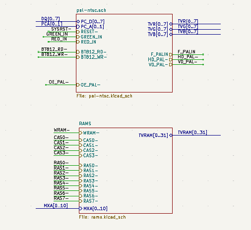
The subsheets are drawn as sheet symbols in the root sheet, meaning they are placed under the root sheet in the schematic hierarchy.
Reusing hierarchical subsheets
The multichannel demo project is an example of using a subsheet multiple times. The root sheet contains four subsheet symbols, which both refer to the same sheet file (channel_strip.kicad_sch). This allows the design to include four copies of the same audio mixer channel circuit. Although the four sheet symbols all refer to the same filename, the sheet names are unique (CH1, CH2, CH3, and CH4). Inside each subsheet the circuits are identical except for the reference designators, which as always are unique. The subsheets each have a single hierarchical label/pin connection to the root sheet, which contains the summing amplifier circuit that combines the output of each channel.
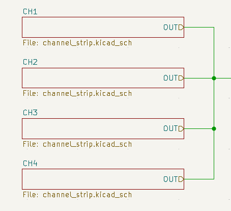
The subsheets are drawn as sheet symbols in the root sheet, meaning they are placed under the root sheet in the schematic hierarchy.
Inspecting a schematic
Find tool
The Find tool searches for text in the schematic, including reference designators, pin names, symbol fields, and graphic text. When the tool finds a match, the canvas is zoomed and centered on the match and the text is highlighted. Launch the tool using the ![]() button in the top toolbar.
button in the top toolbar.
The Find tool has several options:
-
Match case: Selects whether the search is case-sensitive.
-
Whole words only: When selected, the search will only match the search term with complete words in the schematic. When unselected, the search will match if the search term is part of a larger word in the schematic.
-
Regular Expression: When selected, regular expressions can be used in the search terms.
-
Search pin names and numbers: Selects whether the search should apply to pin names and numbers.
-
Search net names: Selects whether the search should apply to net names (labels, symbol pins, sheet pins, and bus members).
-
Include hidden fields: Selects whether the search should apply only to visible fields or if it should include hidden symbol fields.
-
Search the current sheet only: Selects whether the search should be limited to the current schematic sheet.
-
Search the current selection only: Selects whether the search should be limited to the current selection.
There is also a Find and Replace tool which is activated with the ![]() button in the top toolbar. This tool behaves the same as the Find tool, but additionally can replace some or all matches with different text.
button in the top toolbar. This tool behaves the same as the Find tool, but additionally can replace some or all matches with different text.
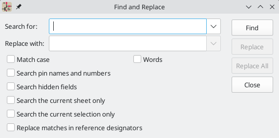
The Find and Replace tool has the same options as the Find tool, with one addition:
-
Replace matches in reference designators: When selected, reference designators will be modified if they contain matching text. Otherwise reference designators will not be affected.
Search panel
The search panel is a docked panel that lists information about symbols, text, labels, and groups from the schematic. Show or hide the search panel with View → Panels → Search or use the Ctrl+G shortcut.
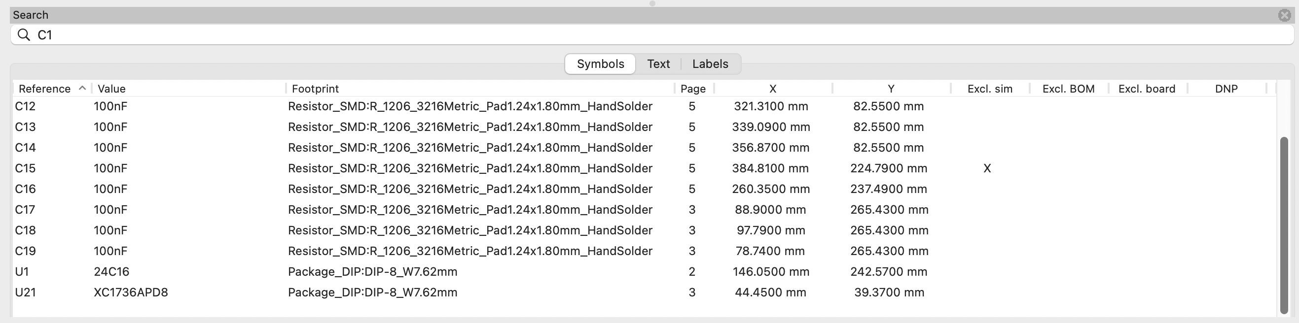
You can optionally filter the list based on a search string. When no filter is used, all items in the design are listed in the corresponding tab. Items from the entire schematic are listed, not just items in the current sheet. Items are filtered based on their properties:
-
Symbols and power symbols are filtered by the contents of their fields. You can select whether to search hidden fields by enabling the Search Hidden Fields option in the
 menu. Symbols are also filtered by their metadata (library link, description, and keywords) if Search Metadata is enabled in the menu.
 -
Text (text and textboxes) is filtered by the text content.
-
Labels are filtered by their netnames.
-
Groups are filtered by the group name.
You can sort the filtered results in ascending or descending order of the value in a particular column by clicking on that column header.
Filters support wildcards: * matches any characters, and ? matches any single character. You can also use regular expressions, such as /symbol value/.
The displayed information depends on the item type:
-
All items list their name and/or value, page number, and X/Y location in the sheet as applicable.
-
Symbols additionally list their reference designator, footprint, attributes (Exclude from Simulation, Exclude from BOM, Exclude from Board, and Do Not Populate), library link (library name and symbol name), and description.
-
Power symbols additionally list their reference designator.
-
Text and labels additionally list their type, e.g. textbox or hierarchical.
When you click an item in the search panel, the schematic editor switches to the item’s schematic sheet, and the item is selected in the editing canvas. Depending on what is configured in the ![]() menu, the schematic editor will also pan and/or zoom to the selected item in the editing canvas. Double-clicking an item in the search panel opens its properties dialog.
menu, the schematic editor will also pan and/or zoom to the selected item in the editing canvas. Double-clicking an item in the search panel opens its properties dialog.
Net highlighting
An electrical net can be highlighted in the schematic editor to visualize all of the places it appears in the schematic. Net highlighting can be activated in the Schematic Editor or by highlighting the corresponding net in the PCB editor when cross-probe highlighting is enabled (see below). When net highlighting is active, the highlighted net will be shown in a different color. By default this color is pink, but it is configurable in the Color section of the Preferences dialog.
Nets can be highlighted by clicking on a wire or pin using the Highlight Net tool in the right toolbar (![]() ). Alternatively, the Highlight Net hotkey (`) highlights the net under the cursor.
). Alternatively, the Highlight Net hotkey (`) highlights the net under the cursor.
Net highlighting can be cleared by using the Clear Net Highlight action (hotkey ~) or by using the Highlight net tool on an empty region in the schematic. By default, Esc also clears net highlighting, but this can be disabled if desired in Preferences → Schematic Editor → Editing Options.
Net navigator
The net navigator is a docked panel that shows the location of every occurrence of a highlighted net in a schematic. Show or hide the net navigator with View → Panels → Net Navigator.
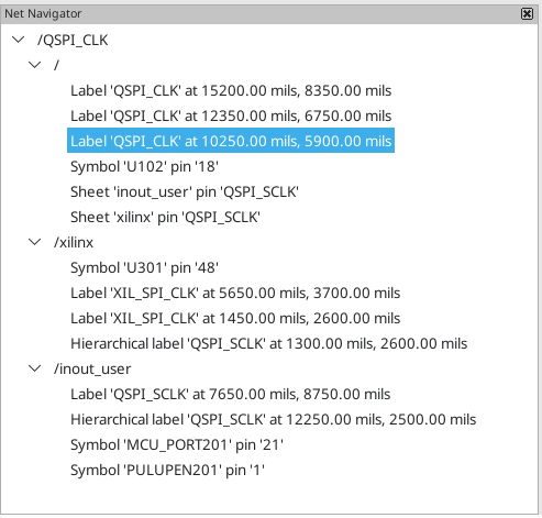
When you highlight a net in the schematic, every place where that net is shown in the schematic is listed in the net navigator panel. All labels, symbol pins, and sheet pins connected to the net are listed. Each occurrence is sorted under its schematic sheet. Clicking on an occurrence displays that item in the editing canvas.
When no net is highlighted, the net navigator displays this information for all nets in the schematic.
| The net navigator displays highlighted nets, not selected nets. |
You can filter the displayed nets by typing part of a net name in the Filter nets textbox. If Wildcard Search is enabled in the ![]() menu, you can use wildcards in the filter string:
menu, you can use wildcards in the filter string: * matches any characters, and ? matches any single character. If Regex Search is enabled instead, you can use regular expressions.
With the net navigator open and a net highlighted, you can quickly select various items on that net (net labels, sheet pins, and symbol pins) by selecting one of the items on the highlighted net in the schematic canvas and pressing Tab/Shift+Tab to cycle through the net items. Pressing Tab selects the next item on the net, while Shift+Tab selects the previous item.
Cross-probing from the PCB
KiCad allows bi-directional cross-probing between the schematic and the PCB. There are several different types of cross-probing.
Selection cross-probing allows you to select a symbol or pin in the schematic to select the corresponding footprint or pad in the PCB (if one exists) and vice-versa.
Cross-probing also works in the 3D Viewer. When a component is selected in the 3D Viewer, it is also selected in the schematic and PCB, and when a component is selected in the schematic or PCB, it is also selected in the 3D Viewer.
By default, cross-probing will result in the display centering on the cross-probed item and zooming to fit. You can disable the centering and zooming behavior, or disable selection cross-probing entirely, in the Display Options section of the Preferences dialog. When the Flash cross-probed selection setting is enabled, selection cross probing will cause the cross-probed item to flash three times, making it easier to spot.
Even when selection cross-probing is disabled, you can manually cross-probe from the schematic to the PCB by right-clicking an object and selecting Select on PCB, or from the PCB to the schematic by right-clicking an object and choosing Select → Select on Schematic.
Highlight cross-probing allows you to highlight a net in the schematic and PCB at the same time. If the option "Highlight cross-probed nets" is enabled in the Display Options section of the Preferences dialog, highlighting a net or bus in the schematic editor will cause the corresponding net or nets to be highlighted in the PCB editor, and vice versa.
Electrical rules checking
The Electrical Rules Checker (ERC) tool checks for certain errors in your schematic, such as unconnected pins, unconnected hierarchical symbols, shorted outputs or other illegal connections, etc. ERC violations are reported as errors or warnings depending on the severity of the issue detected.
ERC does not detect all errors, but it can detect many common issues and oversights. All detected issues should be checked and addressed before proceeding. The quality of the ERC is directly related to the care taken in declaring electrical pin properties during symbol creation. If symbols are designed incorrectly, ERC will not report accurate information.
ERC can be started by clicking on the ![]() button in the top toolbar and clicking the Run ERC button.
button in the top toolbar and clicking the Run ERC button.
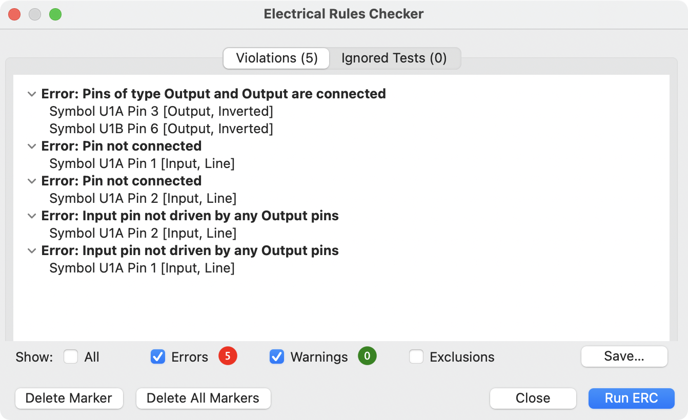
Any warnings or errors are reported in the Violations tab, and markers for each violation are placed in the schematic so that they point to the relevant part of the schematic. Warnings are indicated by yellow arrows, and errors have red arrows. Excluded violations are shown as green arrows. A list of the ignored tests are shown in the Ignored Tests tab. A report file in plain text format can be created after running DRC using the Save… button.
|
Selecting a violation in the ERC window jumps to the selected violation
marker in the schematic, according to the settings in the |
Certain types of violations have contextual actions in the context menu. For example, unannotated symbol violations have an action to run the annotation tool on the violating items. For schematic vs. library symbol mismatch violations, there is an action to run the Compare Symbol with Library tool and another action to update the symbol from the library. These actions can help to quickly fix or identify the reason for a particular violation.
The numbers at the bottom of the window show the number of errors, warnings, and exclusions. Each type of violation can be filtered from the list using the respective checkboxes. Clicking Delete Marker will clear the selected violation until ERC is run again, while clicking Delete All Markers will clear all violations until the next ERC run.
Violations can be right-clicked in the dialog to ignore them or change their severity:
-
Exclude this violation: ignores this particular violation, but does not affect any other violations. You can un-exclude a violation by right clicking the excluded violation and selecting Remove exclusion for this violation.
-
Exclude with comment…: the same as Exclude this violation, but prompts for a comment explaining the reason for the exclusion. When excluded violations are unhidden (using the Exclusions checkbox), exclusion comments are shown with the corresponding excluded violation. To edit an existing exclusion comment or add a comment to an existing exclusion, right click an excluded violation and select Edit exclusion comment….
-
Change severity: changes a type of violation from warning to error, or error to warning. This affects all violations of a given type.
-
Ignore all: ignores all violations of a given type. This test will now appear in the Ignored Tests tab rather than the Violations tab. You can un-ignore the test again by right clicking the test in the Ignored Tests tab, or in the Violation Severity panel in Schematic Setup.
-
Edit violation severities…: opens the Violation Severity panel in Schematic Setup, for editing the severities of all DRC violation types.
You can also exclude the selected marker with Inspect → Exclude Marker, and show or hide each category of marker (errors, warnings, and exclusions) with the View menu.
Excluded and ignored violations are remembered between runs of the design rule checker. Excluded violations are hidden unless the Exclusions checkbox is enabled. Ignored violations are not shown, but there is a list of ignored tests in the Ignored Tests tab.
ERC example
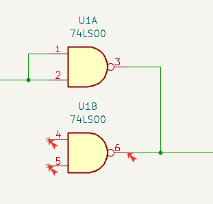
There are three errors in the screenshot above.
-
Two outputs have been connected together (red arrow at right).
-
Two inputs have been left unconnected (red arrows at left). This is actually two errors per pin: each pin is unconnected, and each pin is an input pin that is not driven by an output pin.
Selecting an ERC marker displays a description of the violation in the message pane at the bottom of the window.
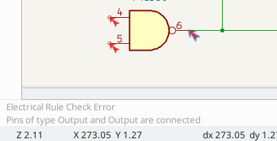
Per-net ERC markers
Some violations are reported only once per net. For example, the "Input Power pin not driven by any Output Power pins" error technically applies to each Input Power pin on an un-driven net, but only one marker is shown per net. This is to avoid producing a large number of markers for a single root cause. In this case, exactly where the marker is placed in the schematic is arbitrary and does not necessarily indicate the ideal location for fixing the issue.
|
All errors for a given net will be reported when the Show all errors option is enabled in the |
In the example below, there are four un-driven Input Power pins (one per power symbol), but only two ERC markers. Adding two PWR_FLAG symbols, one to each un-driven net, will clear the errors. The "correct" location for the PWR_FLAG symbol depends on the schematic and may not be near the particular power symbol where the marker was placed, or even in the same schematic sheet.
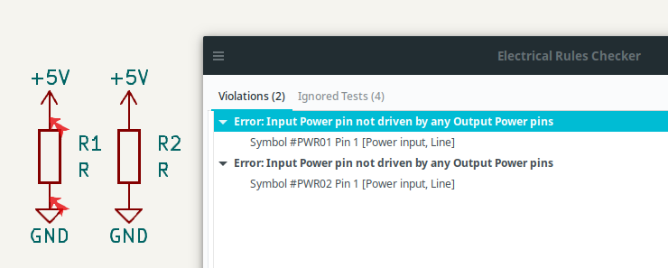
Power pins and power flags
It is common to have an "Input Power pin not driven by any Output Power pins" error on power pins, as shown in the example below, even though the power pins seem to be properly connected to a power rail. This happens in designs where the power is provided through connectors or other components that are not marked as power outputs. In these cases ERC won’t detect any Output Power pins connected to the net and will determine the Input Power pin is not driven by a power source.
For example, in the below schematic, VCC and GND are connected to a connector with passive pins, so the Input Power pins of U1 are not considered driven by a power source.
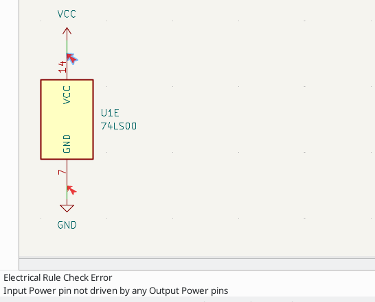
To avoid this warning, connect the net to PWR_FLAG symbol on such a power net as shown in the following example. The PWR_FLAG symbol is found in the power symbol library. Alternatively, connect any Output Power pin to the net; PWR_FLAG is simply a symbol with a single Output Power pin.
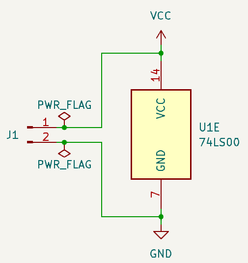
Ground nets often need a PWR_FLAG to be manually added, even when power rails do not, because voltage regulators have outputs declared as Output Power, but their ground pins are typically marked as Power Inputs. Therefore grounds are not considered driven by these voltage regulators. This is so multiple regulators can share a common ground without errors caused by two Output Power pins being connected together.
Power nets do not "jump" across components, so, components like passive inline filtering elements may need a PWR_FLAG on their downstream side to indicate that the net is still connected to a power source.
In the below schematic, although there is a PWR_FLAG on the nets connected to the connectors (VCC_IN and GND_IN), a PWR_FLAG is also needed to mark each of VCC and GND as power nets, because the filter FL1 has only Passive pins.
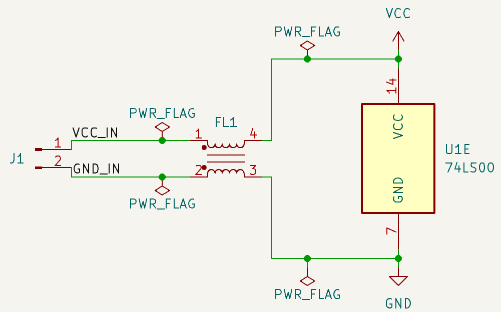
This would be the case also if the VCC_IN and GND_IN nets were connected to a symbol with Output Power pins. In fact, in this schematic, the PWR_FLAG symbols are on VCC_IN and GND_IN are not required, as there are no Input Power pins on those nets.
For more information about power pins and power flags, see the PWR_FLAG documentation.
ERC Configuration
The Violation Severity panel in Schematic Setup lets you configure what types of ERC messages should be reported as Errors, Warnings, or ignored.
The Pin Conflicts Map panel in Schematic Setup allows you to configure connectivity rules to define electrical conditions for errors and warnings based on what types of pins are connected to each other. For example, by default an error is produced when an output pin is connected to another output pin.
Rules can be changed by clicking on the desired square of the matrix, causing it to cycle through the choices: allowed, warning, error.
List of ERC checks
The table below lists the electrical rules that KiCad checks and the default violation severity for each check. All severities are configurable.
Connections ERC checks
These ERC checks look for issues with wire and label connections in the schematic.
| Violation | Descripción | Default Severity |
|---|---|---|
Pin not connected |
This violation occurs when a symbol pin is not connected to a net, unless the pin has a no-connect flag or has electrical type Unconnected. |
Error |
Input pin not driven by any Output pins |
This violation occurs when a symbol pin with electrical type Input is not connected to a driving pin. Driving pins are pins with the type output, bidirectional, tristate, power output, or passive pins. |
Error |
Input Power pin not driven by any Output Power pins |
This violation occurs when a symbol pin with electrical type Input Power is not connected to an Output Power pin. A common cause of this violation is described above. |
Error |
A pin with a "no connection" flag is connected |
The violation occurs when a symbol pin with a no connection flag is connected to a net. |
Aviso |
Unconnected "no connection" flag |
This violation occurs when a No connection flag is not connected to a pin or label. |
Aviso |
Label not connected |
This violation occurs when a global, hierarchical, local, or directive label is not connected to a pin or another label. |
Error |
Label connected to only one pin |
This violation occurs when a label is connected to a net with fewer than two symbol pins on it. This indicates the label isn’t being used to connect anything, as it it is only connected to a single symbol pin. |
Aviso |
Global label only appears once in the schematic |
This violation occurs when a global label only appears once in the schematic, meaning that the label is not forming any global connections. This violation is ignored by default to allow users to use global labels to label nets, even if the net does not connect anywhere else. |
Ignore |
Local and global labels have the same name |
This violation occurs when a local label has the same name as a global label. If these labels are on separate sheets, they will not connect, although they may have been intended to connect. Note that while a local label and a global label with the same name won’t connect if they are on different sheets, they will connect if they are on the same sheet. |
Aviso |
Local and global power symbols have the same name |
This violation occurs when a local power symbol has the same name as a global symbol. If these power symbols are on separate sheets, they will not connect, although they may have been intended to connect. Note that while a local symbol and a global power symbol with the same name won’t connect if they are on different sheets, they will connect if they are on the same sheet. |
Aviso |
Wires not connected to anything |
This violation occurs when a wire is not connected to any pin or label. |
Error |
Bus Entry needed |
This violation only applies to projects imported from EAGLE projects. It indicates places where the importer was unable to automatically add bus entries to the imported schematic, so you must add them by hand. |
Error |
Symbol pin or wire end off connection grid |
This violation occurs when a symbol pin or wire end is not aligned to the connection grid. Symbol pins and wire ends need to be aligned to the grid in order to connect to each other. The grid used for this check is defined by the connection grid setting in Schematic Setup → Formatting → Connection grid. |
Aviso |
Four connection points are joined together |
This violation occurs when wires join in a four-way (cross) junction. Such junctions are sometimes considered harmful because it can be unclear if all four wires are intended to be joined or if two wires were intended to cross without a junction. |
Ignore |
Duplicate pins with different nets |
This violation occurs when two pins in the same symbol have the same pin number but are connected to different nets. Symbol pins do not need to be uniquely numbered within a symbol, but all pins with the same pin number need to be connected to the same net. This violation is always an error. |
Error (not configurable) |
Label connects more than one wire |
This violation occurs when a label anchor connects to two wires (where two wires cross without connecting). In this situation is not possible to determine which net the label should connect to. |
Aviso |
Unconnected wire endpoint |
This violation occurs when a wire endpoint is not connected to anything. |
Aviso |
Conflicts ERC checks
These ERC checks look for conflicting information in symbols, sheets, and buses.
| Violation | Descripción | Default Severity |
|---|---|---|
Duplicate reference designators |
This violation occurs when two symbols have the same reference designator. |
Error |
Units of same symbol have different values |
This violation occurs when units of a single symbol have different values. |
Error |
Different footprint assigned in another unit of the symbol |
This violation occurs when units of a single symbol have different assigned footprints. |
Error |
Different net assigned to a shared pin in another unit of the symbol |
This violation occurs when a pin that is shared between multiple units of a symbol is not connected to the same net in each unit. |
Error |
Duplicate sheet names within a given sheet |
This violation occurs when two hierarchical sheets in the same parent sheet have the same name. |
Error |
Mismatch between hierarchical labels and sheet pins |
This violation occurs when a hierarchical label does not have a corresponding hierarchical sheet pin in the parent sheet, or a hierarchical sheet pin does not have a corresponding hierarchical label in the child sheet. |
Error |
More than one name given given to this bus or net |
This violation occurs when a net has multiple labels attached. Nets can only have a single name, so if multiple labels are attached to a net, one name will be selected and used as the canonical name. |
Aviso |
Conflict between bus alias definitions across schematic sheets |
This violation occurs when a bus alias has different members in different sheets. If the same bus alias name is used in multiple sheets, the members of the alias must be the same for each sheet. |
Error |
Buses are graphically connected but share no bus members |
This violation occurs when buses that are graphically connected do not have bus members in common. |
Error |
Invalid connection between bus and net items |
This violation occurs when a bus is connected to a net item, such as a wire, a label referring to a single net, or a sheet pin referring to a single net. Labels and sheet pins can only be connected to buses if they refer to buses rather than individual signals. |
Error |
Net is graphically connected to a bus but not a bus member |
This violation occurs when a net is connected to a bus with a bus entry but the net is not a member of that bus. |
Aviso |
Ground pin not connected to ground net |
This violation occurs when a power input or power output pin with a name containing "GND" is connected to a net with a name that doesn’t contain "GND", but another power pin in the same symbol is connected to a "GND" net. This indicates that the GND pin is likely misconnected. The comparison is case-insensitive, so "GND", "gnd", and any other combination of uppercase and lowercase letters are all considered GND pins/nets. |
Aviso |
Miscellaneous ERC checks
These ERC checks look for other miscellaneous issues in the schematic.
| Violation | Descripción | Default Severity |
|---|---|---|
Pin name resembles stacked pin |
This violation occurs when a symbol’s pin number resembles a stacked pin range but is malformed or invalid, and therefore the pin is not treated as a stacked pin. |
Aviso |
Field name has leading or trailing whitespace |
This violation occurs when a symbol or sheet field starts or ends wth whitespace. Leading or trailing whitespace isn’t necessarily a problem, but it can be undesired and hard to notice. |
Aviso |
Symbol is not annotated |
This violation occurs when a symbol is not annotated with a unique reference designator. |
Error |
Unresolved text variable |
This violation occurs when a text variable ( |
Error |
Undefined netclass |
This violation occurs when a netclass is assigned graphically
(i.e. in the |
Error |
SPICE model issue |
This violation occurs when a SPICE model has a syntax error or other problem. |
Ignore |
Labels are similar (lower/upper case difference only) |
This violation occurs when two labels are similar and differ only by the case of some letters. This may be a typo causing two labels to be disconnected when they are intended to be connected. |
Aviso |
Power pins are similar (lower/upper case difference only) |
This violation occurs when the net names driven by two global power pins are similar and differ only by the case of some letters. This may be a typo causing two global power pins to be disconnected when they are intended to be connected. |
Aviso |
Power pin and label are similar (lower/upper case difference only) |
This violation occurs when a label and the net name driven by a global power pin are similar and differ only by the case of some letters. This may be a typo causing two global power pins to be disconnected when they are intended to be connected. |
Aviso |
Library symbol issue |
This violation occurs when one of several symbol library issues is detected:
|
Aviso |
Symbol doesn’t match copy in library |
This violation occurs when a symbol in the schematic is different than the library version of the symbol. You can compare between the schematic and library versions of the symbol using the Compare Symbol with Library tool, which is available by right clicking the violation in the ERC window. If desired, you can update the schematic symbol to match the library symbol. |
Aviso |
Footprint link issue |
This violation occurs when one of several footprint assignment issues is detected:
|
Aviso |
Assigned footprint doesn’t match footprint filters |
This violation occurs when the footprint assigned to a symbol does not match the symbol’s footprint filters. If the symbol doesn’t have any footprint filters, no violation occurs. |
Aviso |
Symbol has more units than are defined |
This violation occurs when a symbol has more units placed in the schematic than are defined in the symbol. Units in the schematic must correspond exactly to the symbol definition. |
Error |
Symbol has units that are not placed |
This violation occurs when a unit from a multi-unit symbol is not placed in the schematic. Unplaced units will not be connected to anything. |
Aviso |
Symbol has input pins that are not placed |
This violation occurs when a multi-unit symbol has units with input pins that are not placed, so those input pins will not be connected to anything. |
Aviso |
Symbol has bidirectional pins that are not placed |
This violation occurs when a multi-unit symbol has units with bidirectional pins that are not placed, so those input pins will not be connected to anything. |
Aviso |
Symbol has power input pins that are not placed |
This violation occurs when a multi-unit symbol has units with power input pins that are not placed, so those input pins will not be connected to anything. |
Error |
Conflict problem between pins |
This violation occurs when a connection between pins is not allowed per the allowed connections in the Pin Conflicts Map. |
From Pin Conflicts Map |
User-definable ERC violations
You can manually trigger schematic ERC warnings or errors using special text variables. These items will appear as errors or warnings when ERC runs. This can be useful to flag items for later followup or review.
To cause an ERC violation, use the text variable ${ERC_ERROR <violation name>} or ${ERC_WARNING <violation name>} depending on whether an error or warning is desired. You can place this in a text item, text box, or field, including symbol fields, sheet fields, and label fields. When ERC runs, this will generate a ERC violation with the given violation name. These text variables resolve to an empty string in the schematic, and any text after the braces is included in the ERC violation’s description. The text variable must be placed at the start of the text object in order to trigger a violation.
For example, a text item containing ${ERC_ERROR TODO}Calculate resistor value will appear in the board as just the text "Calculate resistor value", and will generate an ERC error named "TODO" with "Calculate resistor value" in the description.
Archivo de reporte ERC
An ERC report file can be generated and saved by clicking the Save… button in the ERC dialog. The file extension for ERC report files is .rpt.
ERC reports can also be generated by the kicad-cli tool in either text (.rpt) format or JSON.
|
Assigning Footprints
Before routing a PCB, footprints need to be selected for every component that will be assembled on the board. Footprints define the copper connections between physical components and the routed traces on a circuit board.
Some symbols come with footprints pre-assigned, but for many symbols there are multiple possible footprints, so the user needs to select the appropriate one.
KiCad offers several ways to assign footprints:
-
Symbol Properties
-
Symbol Properties Dialog
-
Symbol Fields Table
-
-
While placing symbols
-
Footprint Assignment Tool
Each method will be explained below. Which to use is a matter of preference; one method may be more convenient depending on the situation. All of these methods are equivalent in that they store the name of the selected footprint in the symbol’s Footprint field.
| The Footprint Library Table needs to be configured before footprints can be assigned. For information on configuring the Footprint Library Table, please see the PCB Editor manual. |
Assigning Footprints in Symbol Properties
A symbol’s Footprint field can be edited directly in the symbol’s Properties window.
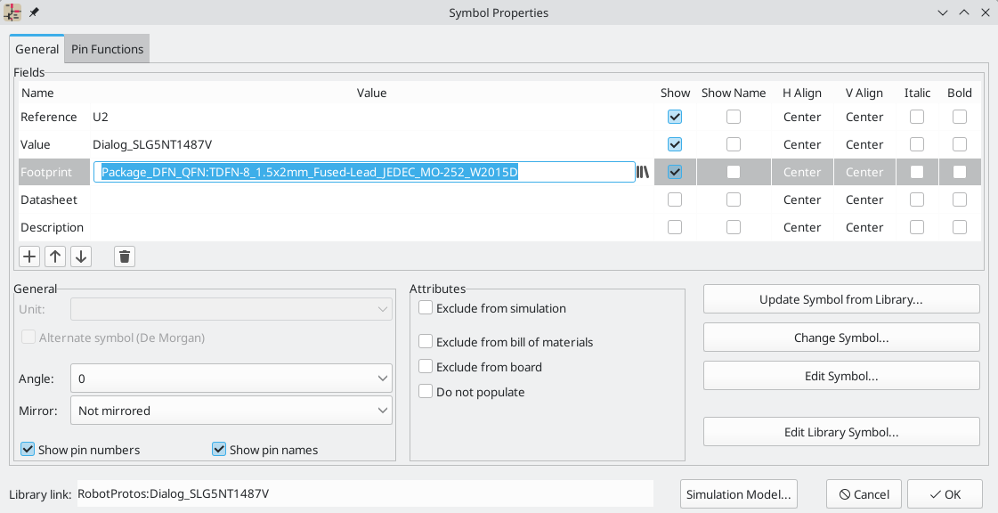
Clicking the ![]() button in the
button in the Footprint field opens the Footprint Chooser, which shows the available footprints sorted by footprint libraries.
The Footprint Chooser filters footprints by name, description, and keywords, as well as any fields that are shown as columns, according to what you type into the search field. * and ? wildcards are available. The footprint search behaves the same as in the symbol chooser dialog. You can choose to sort search results alphabetically or by best match using the options in the ![]() menu.
menu.
If the symbol defines any footprint filters, the apply footprint filters option can be used to hide footprints that don’t match those filters. If the filter by pin count option is selected, only footprints that match the symbol’s pincount will be listed.
Single clicking a footprint name selects the footprint, shows its name, description, and keywords in the bottom pane, and displays it in the preview pane on the right. Clicking the ![]() button shows or hides the description pane. You can show and hide 2D and 3D previews of the footprint by clicking the
button shows or hides the description pane. You can show and hide 2D and 3D previews of the footprint by clicking the ![]() and
and ![]() buttons (Show 3D viewer in own window causes the 3D preview to be opened in a new window).
buttons (Show 3D viewer in own window causes the 3D preview to be opened in a new window).
Double clicking on a footprint closes the chooser and sets the symbol’s Footprint field to the selected footprint.
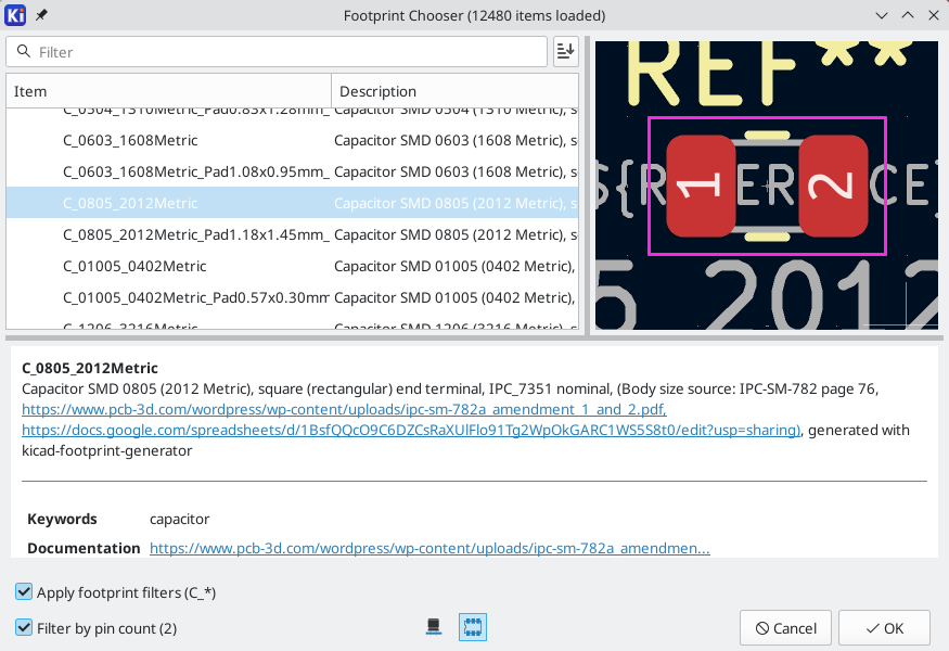
Assigning Footprints with the Symbol Fields Table
Rather than editing the properties of each symbol individually, the Symbol Fields Table can be used to view and edit the properties of all symbols in the design in one place. This includes assigning footprints by editing the Footprint field of each symbol.
The Symbol Fields Table is accessed with Tools → Edit Symbol Fields…, or with the ![]() button on the top toolbar.
button on the top toolbar.
The Footprint field behaves the same here as in the Symbol Properties window: it can be edited directly, or footprints can be selected visually with the Footprint Library Browser.
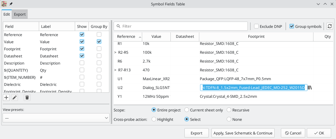
For more information on the Symbol Fields Table, see the section on editing symbol properties.
Assigning Footprints While Placing Symbols
Footprints can be assigned to symbols when the symbol is first added to the schematic.
Some symbols are defined with a default footprint. These symbols will have this footprint preassigned when they are added to the schematic. If a symbol has a default footprint, the footprint will be graphically previewed in the symbol chooser dialog when the symbol is selected. For symbols without a default symbol defined, the footprint dropdown will say "No default footprint", and the footprint preview canvas will say "No footprint specified".
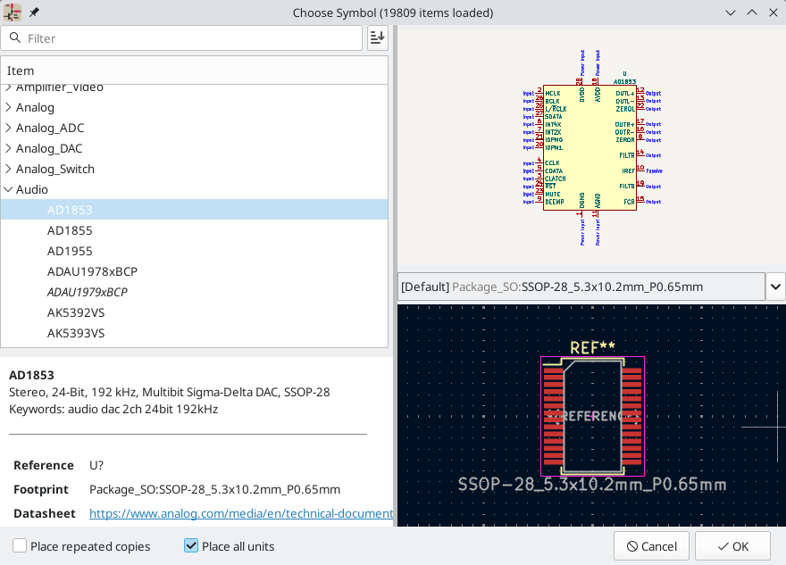
Symbols can have footprint filters that specify which footprints are appropriate to use with that symbol. If footprint filters are defined for the selected symbol, all footprints that match the footprint filters will appear as options in the footprint dropdown. The selected footprint will be displayed in the preview canvas and will be assigned to the symbol when the symbol is added to the schematic.
| Footprint options will not appear in the footprint dropdown unless the footprint libraries are loaded. Footprint libraries are loaded the first time the Footprint Editor or Footprint Library Browser are opened in a session. |
For more information on footprint filters, see the Symbol Editor Documentation.
Assigning Footprints with the Footprint Assignment Tool
The Footprint Assignment Tool allows you to associate symbols in your schematic to footprints used when laying out the printed circuit board. It provides footprint list filtering, footprint viewing, and 3D component model viewing to help ensure the correct footprint is associated with each component.
Components can be assigned to their corresponding footprints manually or automatically by creating equivalence files (.equ files). Equivalence files are lookup tables associating each component with its footprint.
Run the tool with Tools → Assign Footprints…, or by clicking the ![]() icon in the top toolbar.
icon in the top toolbar.
Footprint Assignment Tool Overview
The image below shows the main window of the Footprint Assignment Tool.
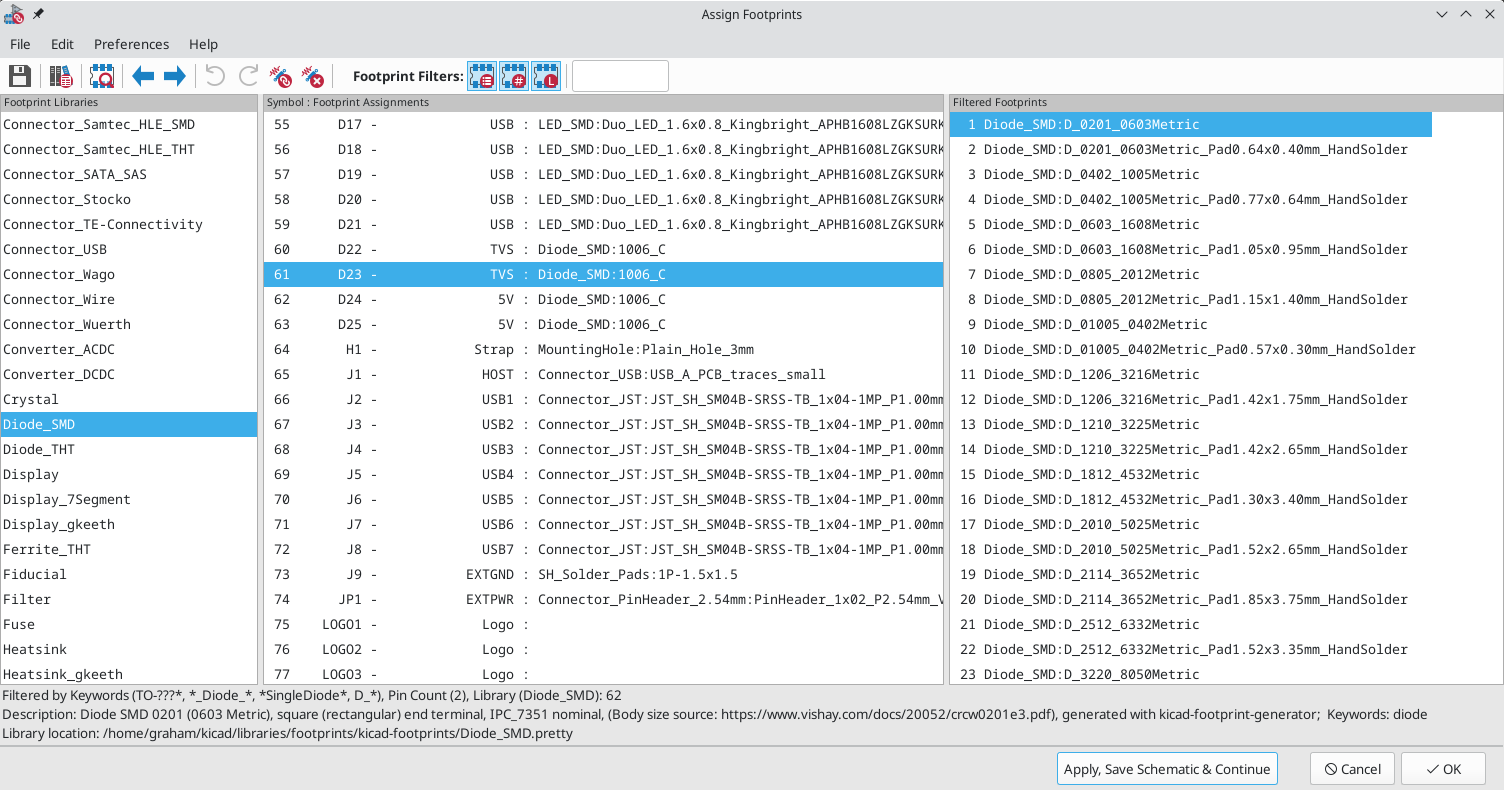
-
The left pane contains the list of available footprint libraries associated with the project.
-
The center pane contains the list of symbols in the schematic.
-
The right pane contains the list of available footprints loaded from the project footprint libraries.
-
The bottom pane describes the filters that have been applied to the footprint list and prints information about the footprint selected in the rightmost pane.
The top toolbar contains the following commands:
|
Transfer the current footprint associations to the schematic. |
|
Edit the global and project footprint library tables. |
|
View the selected footprint in the footprint viewer. |
|
Select the previous symbol without a footprint association. |
|
Select the next symbol without a footprint association. |
|
Undo last edit. |
|
Redo last edit. |
|
Perform automatic footprint association using an equivalence file. |
|
Delete all footprint assignments. |
|
Filter footprint list by footprint filters defined in the selected symbol. |
|
Filter footprint list by pin count of the selected symbol. |
|
Filter footprint list by selected library. |
The following table lists the keyboard commands for the Footprint Assignment Tool:
Right Arrow / Tab |
Activate the pane to the right of the currently activated pane. Wrap around to the first pane if the last pane is currently activated. |
Left Arrow |
Activate the pane to the left of the currently activated pane. Wrap around to the last pane if the first pane is currently activated. |
Up Arrow |
Select the previous item of the currently selected list. |
Down Arrow |
Select the next item of the currently selected list. |
Page Up |
Select the item one full page upwards of the currently selected item. |
Page Down |
Select the item one full page downwards of the currently selected item. |
Home |
Select the first item of the currently selected list. |
End |
Select the last item of the currently selected list. |
Manually Assigning Footprints with the Footprint Assignment Tool
To manually associate a footprint with a component, first select a component in the component (middle) pane. Then select a footprint in the footprint (right) pane by double-clicking on the name of the desired footprint. The footprint will be assigned to the selected component, and the next component without an assigned footprint is automatically selected.
| If no footprints appear in the footprint pane, check that the footprint filter options are correctly applied. |
When all components have footprints assigned to them, click the OK button to save the assignments and exit the tool. Alternatively, click Cancel to discard the updated assignments, or Apply, Save Schematic & Continue to save the new assignments without exiting the tool.
Filtrando la lista de huellas
There are four filtering options which restrict which footprints are displayed in the footprint pane. The filtering options are enabled and disabled with three buttons and a textbox in the top toolbar.
-
 : Activate filters that can be defined in each symbol. For example, an opamp symbol might define filters that show only SOIC and DIP footprints.
 -
 : Only show footprints that match the selected symbol’s pin count.
 -
 : Only show footprints from the library selected in the left pane.
 -
Entering text in the textbox hides footprints that do not match the text. This filter is disabled when the box is empty.
When all filters are disabled, the full footprint list is shown.
The applied filters are described in the bottom pane of the window, along with the number of footprints that meet the selected filters. For example, when the symbol’s footprint filters and pin count filters are enabled, the bottom pane prints the footprint filters and pin count:
Multiple filters can be used at once to help narrow down the list of possibly appropriate footprints in the footprint pane. The symbols in KiCad’s standard library define footprint filters that are designed to be used in combination with the pin count filter.
Automatically Assigning Footprints with the Footprint Assignment Tool
The Footprint Assignment Tool allows you to store footprint assignments in an external file and load the assignments later, even in a different project. This allows you to automatically associate symbols with the appropriate footprints.
The external file is referred to as an equivalence file, and it stores a mapping of a symbol value to a corresponding footprint. Equivalence files typically use the .equ file extension. Equivalence files are plain text files with a simple syntax, and must be created by the user using a text editor. The syntax is described below.
You can select which equivalence files to use by clicking Preferences → Manage Footprint Association Files in the Footprint Assignment Tool.
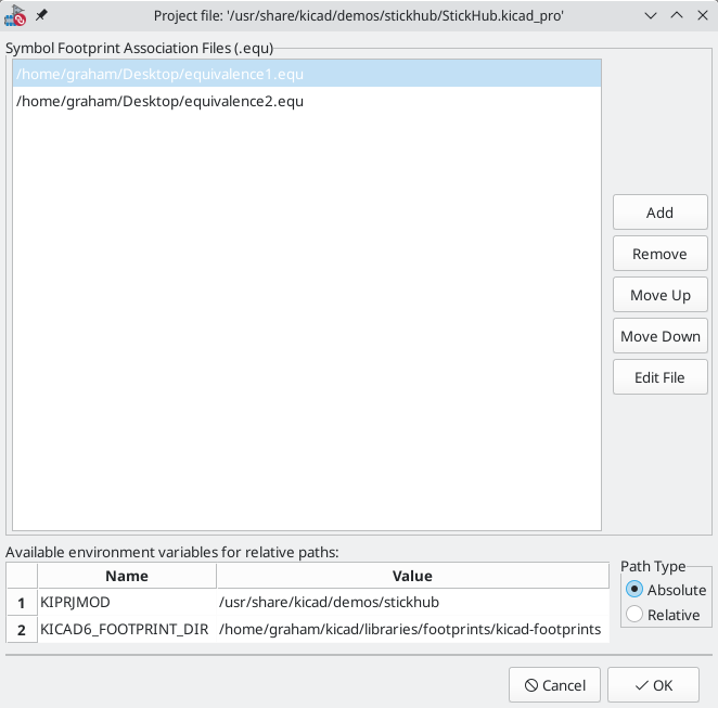
-
Add new equivalence files by clicking the Add button.
-
Remove the selected equivalence file by clicking the Remove button.
-
Change the priority of equivalence files by clicking the Move Up and Move Down buttons. If a symbol’s value is found in multiple equivalence files, the footprint from the last matching equivalence file will override earlier equivalence files.
-
Open the selected equivalence file by clicking the Edit File button.
Relevant environment variables are shown at the bottom of the window. When the Relative path option is checked, these environment variables will automatically be used to make paths to selected equivalence files relative to the project or footprint libraries.
Once the desired equivalence files have been loaded in the correct order, automatic footprint association can be performed by clicking the ![]() button in the top toolbar of the Footprint Assignment Tool.
button in the top toolbar of the Footprint Assignment Tool.
All symbols with a value found in a loaded equivalence file will have their footprints automatically assigned. However, symbols that already have footprints assigned will not be updated.
Formatos de los Archivos de Equivalencia
Equivalence files consist of one line for each symbol value. Each line has the following structure:
'<symbol value>' '<footprint library>:<footprint name>'
Each name/value must be surrounded by single quotes (') and separated by one or more spaces. Lines starting with # are comments.
For example, if you want all symbols with the value LM4562 to be assigned the footprint Package_SO:SOIC-8_3.9x4.9_P1.27mm, the line in the equivalence file should be:
'LM4562' 'Package_SO:SOIC-8_3.9x4.9_P1.27mm'
Aquí se muestra un ejemplo de archivo de equivalencia:
#integrated circuits (smd):
'74LV14' 'Package_SO:SOIC-14_3.9x8.7mm_P1.27mm'
'EL7242C' 'Package_SO:SOIC-8_3.9x4.9_P1.27mm'
'DS1302N' 'Package_SO:SOIC-8_3.9x4.9_P1.27mm'
'LM324N' 'Package_SO:SOIC-14_3.9x8.7mm_P1.27mm'
'LM358' 'Package_SO:SOIC-8_3.9x4.9_P1.27mm'
'LTC1878' 'Package_SO:MSOP-8_3x3mm_P0.65mm'
'24LC512I/SM' 'Package_SO:SOIC-8_3.9x4.9_P1.27mm'
'LM2903M' 'Package_SO:SOIC-8_3.9x4.9_P1.27mm'
'LT1129_SO8' 'Package_SO:SOIC-8_3.9x4.9_P1.27mm'
'LT1129CS8-3.3' 'Package_SO:SOIC-8_3.9x4.9_P1.27mm'
'LT1129CS8' 'Package_SO:SOIC-8_3.9x4.9_P1.27mm'
'LM358M' 'Package_SO:SOIC-8_3.9x4.9_P1.27mm'
'TL7702BID' 'Package_SO:SOIC-8_3.9x4.9_P1.27mm'
'TL7702BCD' 'Package_SO:SOIC-8_3.9x4.9_P1.27mm'
'U2270B' 'Package_SO:SOIC-16_3.9x9.9_P1.27mm'

#regulators
'LP2985LV' 'Package_TO_SOT_SMD:SOT-23-5_HandSoldering'
Visualización de la Huella actual
The Footprint Assignment Tool contains a footprint viewer. Clicking the ![]() button in the top toolbar launches the footprint viewer and shows the selected footprint.
button in the top toolbar launches the footprint viewer and shows the selected footprint.
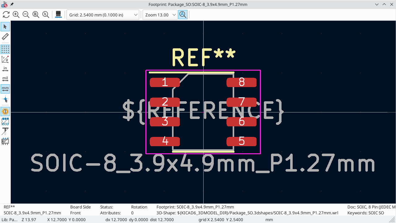
The top toolbar contains the following commands:
|
Refresh view |
|
Zoom in |
|
Zoom out |
|
Zoom to fit drawing in display area |
|
Show 3D viewer |
The left toolbar contains the following commands:
|
Use the select tool |
|
Interactively measure between two points |
|
Display grid dots or lines |
|
Switch between polar and cartesian coordinate systems |
|
Use inches |
|
Display coordinates in mils (1/1000 of an inch) |
|
Display coordinates in millimeters |
|
Toggle display of full-window crosshairs |
|
Toggle between drawing pads in sketch or normal mode |
|
Toggle between drawing pads in normal mode or outline mode |
|
Toggle between drawing text in normal mode or outline mode |
|
Toggle between drawing graphic lines in normal mode or outline mode |
Visualizando el modelo 3D actual
Clicking the ![]() button opens the footprint in the 3D model viewer.
button opens the footprint in the 3D model viewer.
| If a 3D model does not exist for the current footprint, only the footprint itself will be shown in the 3D Viewer. |
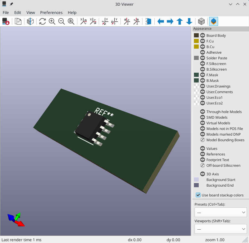
The 3D Viewer is described in the PCB Editor manual.
Forward and back annotation
Update PCB from Schematic (forward annotation)
Use the Update PCB from Schematic tool to sync design information from the Schematic Editor to the Board Editor. The tool can be accessed with Tools → Update PCB from Schematic (F8) in both the schematic and board editors. You can also use the ![]() icon in the top toolbar of the Board Editor. This process is often called forward annotation.
icon in the top toolbar of the Board Editor. This process is often called forward annotation.
| Update PCB from Schematic is the preferred way to transfer design information from the schematic to the PCB. In older versions of KiCad, the equivalent process was to export a netlist from the Schematic Editor and import it into the Board Editor. It is no longer necessary to use a netlist file. |
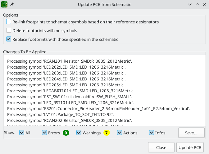
The tool adds the footprint for each symbol to the board and transfers updated schematic information to the board. In particular, the board’s net connections are updated to match the schematic. Symbols with the Exclude from board attribute are not transferred to the PCB.
The changes that will be made to the PCB are listed in the Changes To Be Applied pane. The PCB is not modified until you click the Update PCB button.
You can show or hide different types of messages using the checkboxes at the bottom of the window. A report of the changes can be saved to a file using the Save… button.
Options
The tool has several options to control its behavior.
| Option | Descripción |
|---|---|
Re-link footprints to schematic symbols based on their reference designators |
Footprints are normally linked to schematic symbols via a unique identifier created when the symbol is added to the schematic. A symbol’s unique identifier cannot be changed, but will be lost when the symbol is deleted, even if a symbol with the same reference designator replaces it. If checked, each footprint in the PCB will be re-linked such that each footprint has its unique identifier updated to match the symbol that has the same reference designator as the footprint. This option should generally be left unchecked. See below for more details on when to use this option. |
Group footprints based on symbol group |
If checked, footprints will be added to groups in the PCB if their linked symbols are grouped. |
Replace footprints with those specified by symbols |
If checked, footprints in the PCB will be replaced with the footprint that is specified in the corresponding schematic symbol. If unchecked, footprints that are already in the PCB will not be changed, even if the schematic symbol is updated to specify a different footprint. |
Delete footprints with no symbols |
If checked, any footprint in the PCB without a corresponding symbol in the schematic will be deleted from the PCB. Footprints with the "Not in schematic" attribute will be unaffected. If unchecked, footprints without a corresponding symbol will not be deleted. |
Override locks |
If checked, locking a footprint will not affect whether a footprint is deleted or replaced based on changes in the schematic. If unchecked, locked footprints will never be deleted or replaced even if they otherwise would be. |
Update footprint fields from symbols |
If checked, new and updated fields in symbols will be transferred to the corresponding footprints, keeping symbol and footprint fields in sync. If unchecked, footprint fields will not be updated when fields change in the corresponding symbols. |
Remove footprint fields not found in symbols |
If checked, footprint fields will be removed if they do not exist in the corresponding symbol. If unchecked, footprint fields that do not exist in the corresponding symbol will not be removed, allowing footprints to have additional fields compared to the corresponding symbols. |
Re-linking symbols and footprints
Symbols and footprints are linked together using unique identifiers (also called UUIDs). These are handled automatically within KiCad and are not usually visible to users. They allow a symbol and its partner footprint to keep their connection between schematic and PCB, even if the reference designator is changed. New objects get assigned their identifiers upon creation.
Re-linking by unique identifier (default)
In normal use, the Re-link footprints to schematic symbols based on their reference designators option should be unchecked. In this mode, symbols with the same identifier as a footprint will update that footprint, regardless of the reference designator. Symbols which have an identifier that doesn’t match any footprint will add a new footprint linked to that identifier.
For example, in the below schematic, both R1 and R2 are linked via their unique IDs to footprints on the PCB:
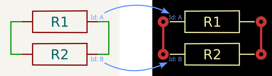
If symbol reference designators are changed in the schematic (e.g. by re-annotation), running the Update PCB from Schematic process will update the reference designators on the PCB.
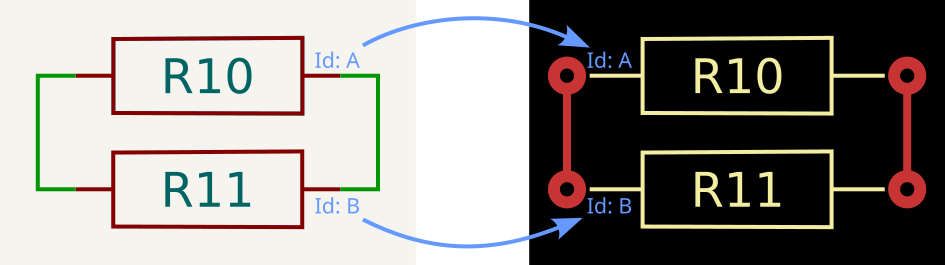
Re-linking by reference designator
If the checkbox is checked, the linking process is done using the reference designators. This can be useful for workflows that result in a symbol being deleted and replaced by another one, rather than being updated in-place. For example, cut-and-pasting a block of schematic or a sheet and copy-pasting and re-annotating will usually break the identifier-based links.
For example in the below case, the resistors R1 and R2 have been deleted and replaced, then re-annotated. While the reference designators are the same, the internal identifiers have changed. Updating the PCB by identifier would cause the existing footprints to be deleted and new ones added - to KiCad, the existing footprints have no matching symbol. This would cause the footprints to lose their positions and need placing again.
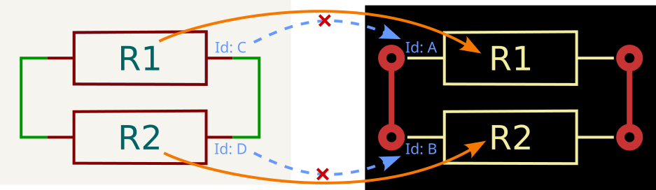
Re-linking the footprints by reference designator causes KiCad to re-create the links, using the matching reference designators as a guide.
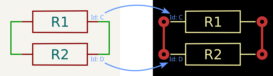
Because the links have been re-established, the next forward annotation should use the normal identifier-based linking (i.e. the checkbox should be unchecked).
Update Schematic from PCB (back annotation)
The typical workflow in KiCad is to make changes in the schematic and then sync the changes to the board using the Update PCB From Schematic tool. However, the reverse process is also possible: design changes can be made in the board and then synced back to the schematic using Tools → Update Schematic From PCB in either the schematic or board editors. This process is also known as backannotation.
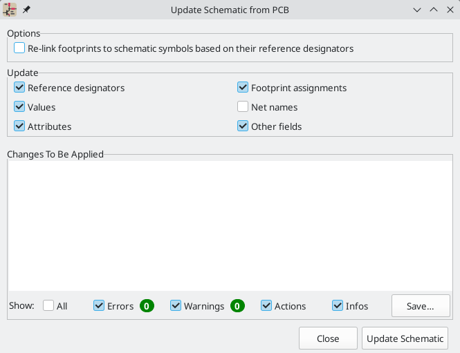
The tool syncs changes in reference designators, values, attributes (like DNP or Exclude From BOM), footprint assignments, other fields, and net names from the board to the schematic. Each type of change can be individually enabled or disabled.
The changes that will be made to the schematic are listed in the Changes To Be Applied pane. The schematic is not modified until you click the Update Schematic button.
You can show or hide different types of messages using the checkboxes at the bottom of the window. A report of the changes can be saved to a file using the Save… button.
Options
The tool has several options to control its behavior.
Option |
Descripción |
Re-link footprints to schematic symbols based on their reference designators |
If checked, each footprint in the PCB will be re-linked to the symbol that has the same reference designator as the footprint. This option is incompatible with updating symbol reference designators. If unchecked, footprints and symbols will be linked by unique identifier as usual, rather than by reference designator. This option should generally be left unchecked. See the PCB Editor documentation for more details on when to use this option. |
Reference designators |
If checked, symbol reference designators will be updated to match the reference designators of the linked footprints. If unchecked, symbol reference designators will not be updated. |
Values |
If checked, symbol values will be updated to match the values of the linked footprints. If unchecked, symbol values will not be updated. |
Attributes |
If checked, symbol attributes (like exclude from BOM and DNP) will be updated to match the corresponding attributes of the linked footprints. If unchecked, symbol attributes will not be updated. |
Other fields |
If checked, other symbol fields will be updated to match the corresponding fields of the linked footprints. Reference designator, value, and footprint are each controlled by their own separate option. If unchecked, other fields will not be updated in the schematic. |
Footprint assignments |
If checked, footprint assignments will be updated for symbols which have had their footprints changed or replaced in the board. If unchecked, symbol footprint assignments will not be updated. |
Net names |
If checked, the schematic will be updated with any net name changes that have been made in the board. Net labels will be updated or added to the schematic as necessary to match the board. If unchecked, net names will not be updated in the schematic. |
Prefer symbol unit swaps over label swaps |
The tool will detect situations where net connections within a multi-unit symbol have changed due to entire symbol units (gates) being swapped. Such swaps will be detected whether they were performed using the PCB Editor’s gate swap tool or whether the equivalent net changes were made manually. If checked, in these situations the schematic will be updated to match the PCB by swapping symbol units rather than swapping the net labels attached to the pins on each symbol unit. If unchecked, symbol unit swaps will be represented in the schematic by swapping net labels rather than swapping symbol units. |
Prefer symbol pin swaps over label swaps |
The tool will detect situations where net connections have swapped between two pins within a symbol. Such swaps will be detected whether they were performed using the pin swap tool or whether the equivalent net changes were made manually. If checked, in these situations the schematic will be updated to match the PCB by swapping symbol pins in the symbol rather than swapping the net labels attached to the pins, if possible. Symbol pins can only be swapped if the Allow unconstrained pin swaps option is enabled in the Editing Options page of the Schematic Editor’s preferences. If unchecked, symbol pin swaps will be represented in the schematic by swapping net labels rather than swapping pins in the symbol. |
| The Geographical Reannotation feature can be used in combination with backannotating reference designators to reannotate all components in the design based on their location in the layout. |
Back annotation with CMP files
Select changes can also be synced from the PCB back to the schematic by exporting a CMP file from the PCB editor (File → Export → Footprint Association (.cmp) File…) and importing it in the Schematic Editor (File → Import → Footprint Assignments…).
| This method can only sync changes made to footprint assignments and footprint fields. It is recommended to use the Update Schematic from PCB tool instead. |
Generating Outputs
Printing
KiCad can print the schematic to a standard printer using File→Print….
Printing options
-
Print drawing sheet: Include the drawing sheet border and title block in the printed schematic.
-
Output mode: Print the schematic in color or black and white.
-
Print background color: Include the background color in the printed schematic. This option is only enabled when printing in color.
-
Use a different color theme for printing: Select a different color scheme for printing than the one selected for display in the Schematic Editor.
-
Page Setup…: Opens a page setup dialog for setting paper size and orientation.
-
Close: Closes the dialog without printing.
-
Print: Opens the system print dialog.
| Printing uses platform- and printer-specific drivers and may have unexpected results. When printing to a file, Plotting is recommended instead of Printing. |
Plotting
KiCad can plot schematics to a file using File → Plot….
The supported output formats are Postscript, PDF, SVG, DXF, and PNG.
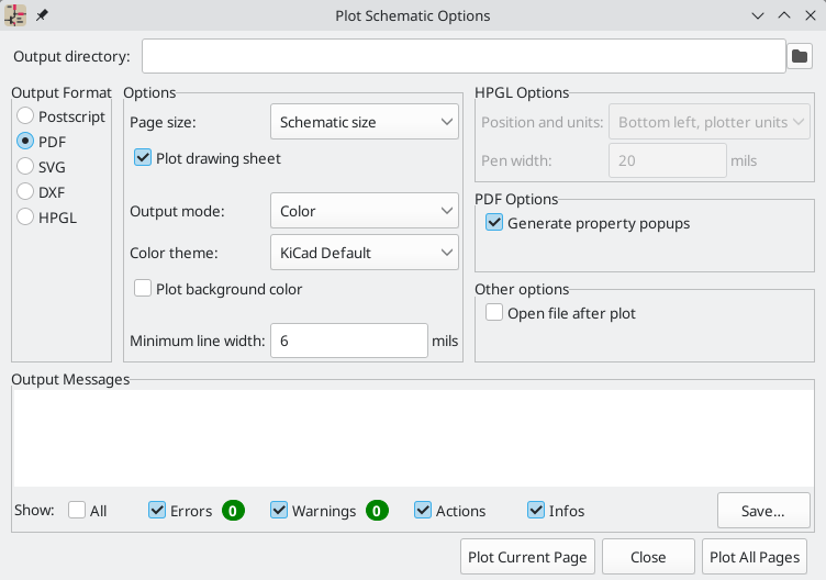
The Output Messages pane displays messages about the generated files. Different kinds of messages can be shown or hidden using the checkboxes, and the messages can be saved to a file using the Save… button.
The Plot Current Page button plots the current page of the schematic. The Plot All Pages button plots all pages of the schematic. One file is generated for each page, except for PDF output, which plots each schematic page as a separate page in a single PDF file.
Plotting options
-
Output directory: Specify the location to save plotted files. If this is a relative path, it is created relative to the project directory. This path can use text variables, including both project text variables and built-in text variables.
-
Design variant: Select the design variant to plot.
-
Output Format: Select the format to plot in. Some formats have different options than others.
-
Page size: Sets the page size to use for the plotted output. This can be set to match the schematic size or to another sheet size.
-
Plot drawing sheet: Include the drawing sheet border and title block in the printed schematic.
-
Output mode: Sets the output to color or black and white. Not all output formats support color.
-
Color theme: Selects the color theme to use for the plotted output.
-
Plot background color: Includes the schematic background color in the plotted output. The background color will not be plotted if the output format does not support color or the output mode is black and white.
-
Minimum line width: Selects the minimum width for lines. Any lines narrower than this width will be plotted with this minimum width.
-
Generate property popups: Enables the interactive PDF features described below. This option only applies for PDF output.
-
Generate clickable links for hierarchical elements: Enables clickable hierarchical sheets, hierarchical sheet pins, and hierarchical labels. When enabled, clicking a hierarchical sheet or sheet pin in the PDF will open the PDF page for that subsheet. Clicking a hierarchical label will open the page for the parent sheet. If Generate property popups is also enabled, links will be generated instead of property popups for hierarchical sheets, pins, and labels (i.e. this option takes priority). This option only applies for PDF output.
-
Generate metadata from AUTHOR and SUBJECT variables: Sets the Author and Subject PDF document properties for the generated PDF based on the
AUTHORandSUBJECTproject text variables, if you have defined them. This option only applies for PDF output. -
Export units: Sets the units (inches or millimeters) in the exported DXF file.
-
DPI: Sets the pixel density of the output file (PNG only).
-
Anti-alias: Controls whether the output file should be anti-aliased (PNG only).
-
Open file after plot: automatically opens the plotted output file when plotting is complete.
Interactive PDF features
Plotted PDFs can optionally have several interactive features.
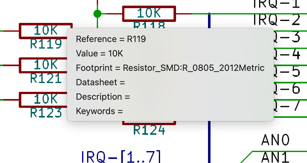
-
Hyperlinks can be clicked.
-
The table of contents is populated with schematic sheets as well as the symbols and hierarchical labels in each sheet.
-
Clicking on many schematic elements displays a popup menu containing relevant information.
-
Symbols display their symbol fields.
-
Hierarchical subsheets display their sheetname and filename, as well as an option to enter the sheet itself. This is replaced by a direct link to the subsheet if the Generate clickable links for hierarchical elements option is enabled.
-
Labels display the resolved net and netclass.
-
Buses display their members.
-
| Some of these features are not supported in all PDF readers. The clickable links generated by the Generate clickable links for hierarchical elements option are more widely supported than other interactive features. |
Generating a bill of materials
KiCad can generate a bill of materials that lists all of the components in the design. BOMs are configurable: you can select which components are included, how components are ordered, which symbol fields are included and in what order, and what the output format is.
BOMs are exported using the Symbol Fields Table. As a shortcut to open the Export tab of this dialog, you can select Tools → Generate Bill of Materials… or use the ![]() button on the top toolbar.
button on the top toolbar.
The contents of the BOM are configured in the Edit tab. The format of the exported BOM file is configured in the Export tab. The BOM is written when you press the Export button at the bottom of the dialog.
BOM contents
The exported BOM will contain the components (rows) and fields (columns) shown in the Edit tab, with the same grouping and sorting.
The Exclude from BOM and Do not Populate attributes affect the Edit tab and the exported BOM as follows:
-
Components with the Exclude from BOM attribute set are always excluded from BOM exports. They are shown in the Edit tab unless the Include 'Exclude from BOM' Symbols option is unchecked in the
menu. -
Components with the Do not Populate (DNP) attribute set are included in BOM exports and shown in the Edit tab unless the Include 'DNP' Symbols option is unchecked in the
menu.
You can filter the components that are exported by typing in the Filter textbox. This matches against symbols' references. Wildcards are supported: * matches any number of any characters, including none, and ? matches any single character.
You can also limit the displayed components to those in the current sheet, the current sheet and all of its subsheets, or the entire schematic using the dropdown menu next to the filter box.
The panel on the left side of the dialog contains a list of columns that are available to show in the Edit tab and include in the BOM. You can collapse this panel by clicking the ![]() button.
button.
Fields with the Include box checked will be shown in the Edit tab and included as columns in the BOM. You can also show or hide columns by right clicking the column header in the right part of the dialog and selecting the desired columns. To reorder the columns, drag a column header to the left or right. You can set an arbitrary name for each column by clicking in the BOM Name column and entering a new name.
Fields with the Group By box checked are used to group components together. Components are grouped into the same line if all of their Group By fields are identical and the Group symbols box at the top of the dialog is checked.
Presets
Presets are available to configure the list of fields. Presets store which fields are displayed, which fields are used for grouping, and the column order. You can create and save your own presets or use one of several default presets. Custom presets can be deleted in this dialog or in the Schematic Setup dialog.
There are several built-in presets:
-
"Grouped By Value" and "Grouped By Value and Footprint" replicate legacy BOM scripts. These group the symbols in the BOM by their
Valuefield and theirValueandFootprintfields, respectively. -
"Attributes" shows only the reference and value fields and the DNP, exclude from board, exclude from simulation, and exclude from BOM attributes.
Virtual fields
Some virtual fields are available that may be useful in BOM exports. Adding a field in the Symbol Fields Table beginning with a text variable will not create a new field in the symbols, but will create a special column in the table and BOM with auto-generated values for each component. The following variables may be especially useful for creating virtual fields in custom BOM formats:
-
${QUANTITY}creates a field that contains the number of grouped instances of that component. -
${ITEM_NUMBER}creates a field that contains the row number of the component in the BOM. -
${SYMBOL_NAME}creates a field that contains the name of the schematic symbol. -
${SYMBOL_LIBRARY}creates a field that contains the name of the schematic symbol library. -
${DNP}creates a field with a checkbox that controls the component’s DNP attribute. In the BOM, this field resolves to the string "DNP" if the component’s DNP attribute is set, or an empty string otherwise. -
${EXCLUDE_FROM_BOARD}creates a field with a checkbox that controls the component’s exclude from board attribute. In the BOM, this field resolves to the string "Excluded from board" if the component’s exclude from board attribute is set, or an empty string otherwise. -
${EXCLUDE_FROM_SIM}creates a field with a checkbox that controls the component’s exclude from simulation attribute. In the BOM, this field resolves to the string "Excluded from simulation" if the component’s exclude from simulation attribute is set, or an empty string otherwise. -
${EXCLUDE_FROM_BOM}creates a field with a checkbox that controls the component’s exclude from BOM attribute. Components with the exclude from BOM attribute set are not included in the BOM.
Other text variables are also available.
The full functionality of the Edit tab, including virtual field behavior, is explained in more detail in the Symbol Fields Table documentation.
BOM format
The Export tab contains settings concerning the output file format for the BOM and displays a preview of the raw BOM file output.
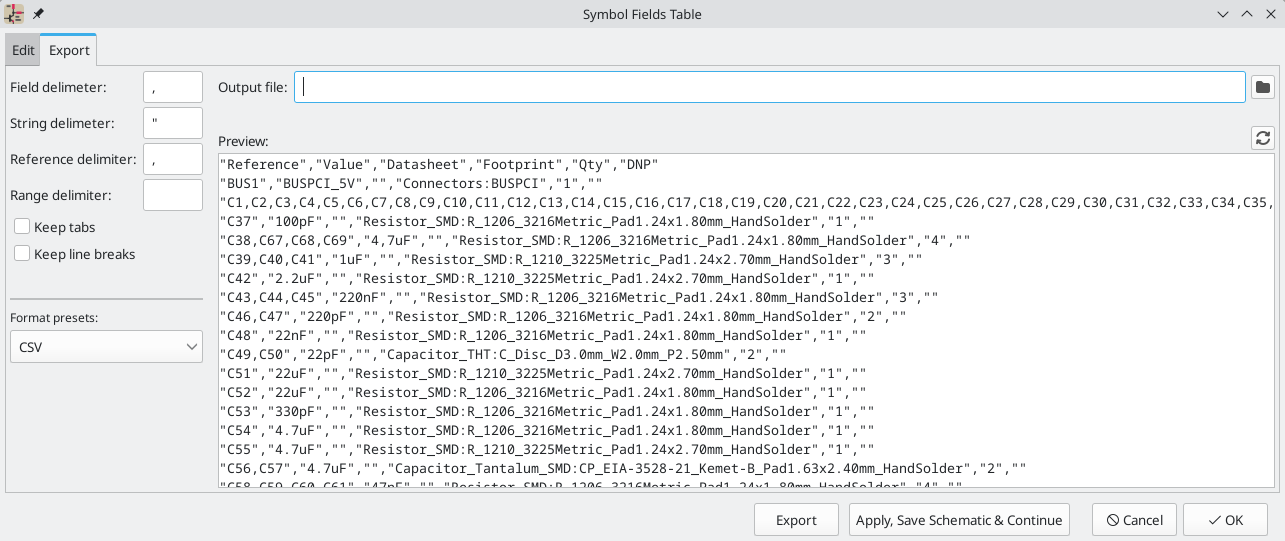
At the top you can specify the output file. Pressing the Export button will write the BOM to this file path. This path can contain text variables.
The settings on the left control how the BOM information is formatted in the file. You can change the delimiter between fields, the delimiter that surrounds each field, the delimiter that separates a sequence of references (e.g. the comma in R1,R3), and the delimiter for a range of references (e.g. the dash in R1-R3). If no range delimiter is given, ranges will not be used: R1-R3 will be written out as R1,R2,R3, for example, assuming , as a reference delimiter. Tabs and newlines in fields can be preserved or stripped, depending on the Keep tabs and Keep line breaks settings.
Several default format presets are available. You can select a comma-separated value (CSV) format, a tab-separated value (TSV) format, or a semicolon-separated format. You can also create and save your own presets. Custom presets can be deleted in this dialog or in the Schematic Setup dialog.
Legacy BOM generation
Previous versions of KiCad used external scripts to process the design information into the desired output format. This BOM generation tool is still available by selecting Tools → Generate Legacy Bill of Materials….
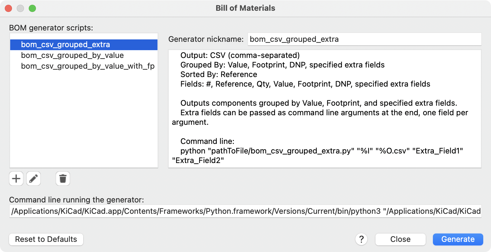
Several BOM generator scripts are included with KiCad, and users can also create their own. BOM generator scripts generally use Python or XSLT, but other tools can be used as long as you can specify a command line for KiCad to execute when running the generator.
You can select which BOM generator to use in the BOM generator scripts list. The rest of the dialog displays information about the selected generator. You can change the displayed name of the generator with the Generator nickname textbox.
The pane at right displays information about the selected script. When the generator is executed, the right pane instead displays output from the script.
The text box at the bottom contains the command that KiCad will use to execute the generator. It is automatically populated when a script is selected, but the command may need to be hand-edited for some generators. KiCad saves the command line for each generator when the BOM tool is closed, so command line customizations are preserved. For more details about the command line, see the advanced documentation.
On Windows, the BOM Generator dialog has an additional option Show console window. When this option is unchecked, BOM generators run in a hidden console window and any output is redirected and printed in the dialog. When this option is checked, BOM generators run in a visible console window, which may be necessary if the generator plugin provides a graphical user interface.
BOM generator scripts
By default, the legacy BOM tool presents three output script options.
-
bom_csv_grouped_extraoutputs a CSV with a single section containing every component in the design. Components are grouped by value, footprint, DNP (do not populate), and any additional fields that are specified on the command line. To specify extra fields, add the desired field names as quoted strings at the end of the command line. For example, to include theMPNfield, the end of the command line would be:<path to script>/bom_csv_grouped_extra.py "%I" "%O.csv" "MPN". The columns in the BOM are:-
Line item number
-
Reference designator(s)
-
Quantity
-
Value
-
Footprint
-
DNP
-
Specified extra fields
-
-
bom_csv_grouped_by_valueoutputs a CSV with two sections. The first section contains every component in the design, with a single component on each line. The second section also contains every component, but components are grouped by symbol name, value, footprint, and DNP (do not populate). The columns in the BOM are:-
Line item number
-
Quantity
-
Reference designator(s)
-
Value
-
Symbol library and symbol name
-
Footprint
-
Datasheet
-
DNP
-
Any other symbol fields
-
-
bom_csv_grouped_by_value_with_fpoutputs a CSV with a single section containing every component in the design. Components are grouped by value, footprint, and DNP (do not populate). The columns in the BOM are:-
Reference designator(s)
-
Quantity
-
Value
-
Symbol name
-
Footprint
-
Symbol description
-
Vendor
-
DNP
-
Additional generator scripts are installed with KiCad but are not populated in the generator script list by default. The location of these scripts depends on the operating system and may vary based on installation location.
| Operating System | Location |
|---|---|
Windows |
|
Linux |
|
macOS |
|
Additional scripts can be added to the list of BOM generator scripts by clicking the ![]() button. Scripts can be removed by clicking the
button. Scripts can be removed by clicking the ![]() button. The
button. The ![]() button opens the selected script in a text editor.
button opens the selected script in a text editor.
For more information on creating and using custom BOM generators, see the advanced documentation.
BOM export from PCB editor
The PCB Editor can export a BOM through File → Fabrication Outputs → BOM…. This method provides no control over the output format and does not include all symbol information, but is useful for PCB-only workflows that do not involve a schematic. In general, it is recommended to use the schematic editor’s BOM export tool instead.
Generating a Netlist
A netlist is a file which describes electrical connections between symbol pins. These connections are referred to as nets. Netlist files contain:
-
A list of symbols and their pins.
-
A list of connections (nets) between symbol pins.
Many different netlist formats exist. Sometimes the symbols list and the list of nets are two separate files. This netlist is fundamental in the use of schematic capture software, because the netlist is the link with other electronic CAD software, such as PCB layout software, simulators, and programmable logic compilers.
KiCad supports several netlist formats:
-
KiCad format, which can be imported by the KiCad PCB Editor. However, the "Update PCB from Schematic" tool should be used instead of importing a KiCad netlist into the PCB editor.
-
OrCAD PCB2 format, for designing PCBs with OrCAD.
-
Allegro format, for designing PCBs with Allegro.
-
PADS format, for designing PCBs with PADS.
-
CADSTAR format, for designing PCBs with CADSTAR.
-
Spice format, for use with various external circuit simulators.
| In KiCad version 5.0 and later, it is not necessary to create a netlist for transferring a design from the schematic editor to the PCB editor. Instead, use the "Update PCB from Schematic" tool. |
| Other software tools that use netlists may have restrictions on spaces and special characters in component names, pins, nets, and other fields. For compatibility, be aware of such restrictions in other tools you plan to use, and name components, nets, etc. accordingly. |
Formatos de Netlist
Netlists are exported with the Export Netlist dialog (File→Export→Netlist…).
KiCad supports exporting netlists in several formats: KiCad, OrcadPCB2, Allegro, PADS, CADSTAR, Spice, and Spice Model. Each format can be selected by selecting the corresponding tab at the top of the window. Some netlist formats have additional options.
Clicking the Export Netlist button prompts for a netlist filename and saves the netlist.
| Netlist generation can take up to several minutes for large schematics. |
Custom generators for other netlist formats can be added by clicking the Add Generator… button. Custom generators are external tools that are called by KiCad, for example Python scripts or XSLT stylesheets. For more information on custom netlist generators, see the section on adding custom netlist generators.
Spice Netlist Format
The Spice netlist format offers several options.
-
When the use current sheet as root is selected, only the current sheet is exported to a subcircuit model. Otherwise, the entire schematic sheet is exported.
-
The Save all voltages option adds a
.save allcommand to the netlist, which causes the simulator to save all node voltages. -
The Save all currents option adds a
.probe allicommand to the netlist, which causes the simulator save all node currents. -
The Save all power dissipations adds
.probecommands to save the power dissipation in each component. -
The Save all digital event data removes the
esave nonecommand from the netlist, which causes digital event data to be saved. Digital event data may consume a lot of memory.
| Exact behavior may vary between simulation tools. |
Passive symbol values are automatically adjusted to be compatible with various Spice simulators. Specifically:
-
μandMas unit prefixes are replaced withuandMeg, respectively -
Units are removed (e.g.
4.7kΩis changed to4.7k) -
Values in RKM format are rewritten to be Spice-compatible (e.g.
4u7is changed to4.7u)
The Spice netlist exporter also provides an easy way to simulate the generated netlist with an external simulator. This can be useful for running a simulation without using KiCad’s internal ngspice simulator, or for running an ngspice simulation with options that are not supported by KiCad’s simulator tool.
Enter the path to the external simulator in the text box, with %I representing the generated netlist. Check the run external simulator command box to generate the netlist and automatically run the simulator.
The default simulator command (spice "%I") must be adjusted to point to
a simulator installed on your system.
|
Spice simulators expect simulation commands (.PROBE, .AC, .TRAN, etc.) to be included in the netlist. Any text line included in the schematic diagram starting with a period (.) will be included in the netlist. If a text object contains multiple lines, only the lines beginning with a period will be included.
.include directives for including model library files are automatically added to the netlist based on the Spice model settings for the symbols in the schematic.
Spice Model Netlist Format
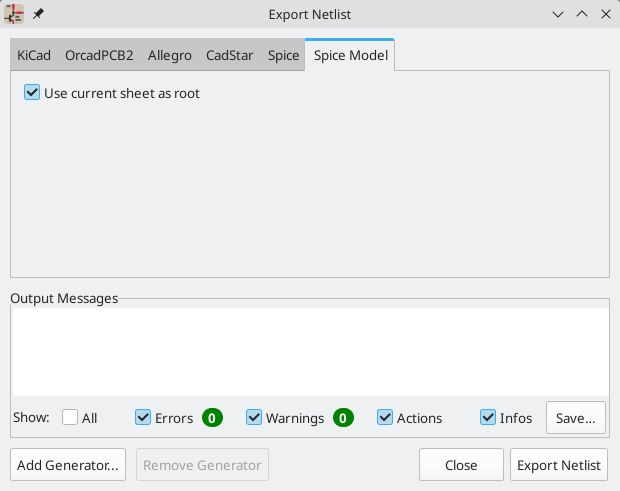
KiCad can also export a netlist of the schematic as a Spice subcircuit model, which can be included in a separate Spice simulation. Any hierarchical labels in the schematic are used as pins for the subcircuit model. Each pin in the model is annotated with a comment describing the pin’s electrical direction:
-
Inputhierarchical labels are mapped to aninputannotation -
Outputhierarchical labels are mapped to anoutputannotation -
Bidirectionalhierarchical labels are mapped to aninoutannotation -
Tri-statehierarchical labels are mapped to atristateannotation -
Passivehierarchical labels are mapped to apassiveannotation
When the use current sheet as root is selected, only the current sheet is exported to a subcircuit model. Otherwise, the entire schematic sheet is exported.
Ejemplos de Netlist
Below is the schematic from the sallen_key project included in KiCad’s simulation demos.
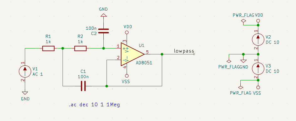
The KiCad format netlist for this schematic is as follows:
(export (version "E")
  (design
    (source "/usr/share/kicad/demos/simulation/sallen_key/sallen_key.kicad_sch")
    (date "Sun 01 May 2022 03:14:05 PM EDT")
    (tool "Eeschema (6.0.4)")
    (sheet (number "1") (name "/") (tstamps "/")
      (title_block
        (title)
        (company)
        (rev)
        (date)
        (source "sallen_key.kicad_sch")
        (comment (number "1") (value ""))
        (comment (number "2") (value ""))
        (comment (number "3") (value ""))
        (comment (number "4") (value ""))
        (comment (number "5") (value ""))
        (comment (number "6") (value ""))
        (comment (number "7") (value ""))
        (comment (number "8") (value ""))
        (comment (number "9") (value "")))))
  (components
    (comp (ref "C1")
      (value "100n")
      (libsource (lib "sallen_key_schlib") (part "C") (description ""))
      (property (name "Sheetname") (value ""))
      (property (name "Sheetfile") (value "sallen_key.kicad_sch"))
      (sheetpath (names "/") (tstamps "/"))
      (tstamps "00000000-0000-0000-0000-00005789077d"))
    (comp (ref "C2")
      (value "100n")
      (fields
        (field (name "Fieldname") "Value")
        (field (name "SpiceMapping") "1 2")
        (field (name "Spice_Primitive") "C"))
      (libsource (lib "sallen_key_schlib") (part "C") (description ""))
      (property (name "Fieldname") (value "Value"))
      (property (name "Spice_Primitive") (value "C"))
      (property (name "SpiceMapping") (value "1 2"))
      (property (name "Sheetname") (value ""))
      (property (name "Sheetfile") (value "sallen_key.kicad_sch"))
      (sheetpath (names "/") (tstamps "/"))
      (tstamps "00000000-0000-0000-0000-00005789085b"))
    (comp (ref "R1")
      (value "1k")
      (fields
        (field (name "Fieldname") "Value")
        (field (name "SpiceMapping") "1 2")
        (field (name "Spice_Primitive") "R"))
      (libsource (lib "sallen_key_schlib") (part "R") (description ""))
      (property (name "Fieldname") (value "Value"))
      (property (name "SpiceMapping") (value "1 2"))
      (property (name "Spice_Primitive") (value "R"))
      (property (name "Sheetname") (value ""))
      (property (name "Sheetfile") (value "sallen_key.kicad_sch"))
      (sheetpath (names "/") (tstamps "/"))
      (tstamps "00000000-0000-0000-0000-0000578906ff"))
    (comp (ref "R2")
      (value "1k")
      (fields
        (field (name "Fieldname") "Value")
        (field (name "SpiceMapping") "1 2")
        (field (name "Spice_Primitive") "R"))
      (libsource (lib "sallen_key_schlib") (part "R") (description ""))
      (property (name "Fieldname") (value "Value"))
      (property (name "SpiceMapping") (value "1 2"))
      (property (name "Spice_Primitive") (value "R"))
      (property (name "Sheetname") (value ""))
      (property (name "Sheetfile") (value "sallen_key.kicad_sch"))
      (sheetpath (names "/") (tstamps "/"))
      (tstamps "00000000-0000-0000-0000-000057890691"))
    (comp (ref "U1")
      (value "AD8051")
      (fields
        (field (name "Spice_Lib_File") "ad8051.lib")
        (field (name "Spice_Model") "AD8051")
        (field (name "Spice_Netlist_Enabled") "Y")
        (field (name "Spice_Primitive") "X"))
      (libsource (lib "sallen_key_schlib") (part "Generic_Opamp") (description ""))
      (property (name "Spice_Primitive") (value "X"))
      (property (name "Spice_Model") (value "AD8051"))
      (property (name "Spice_Lib_File") (value "ad8051.lib"))
      (property (name "Spice_Netlist_Enabled") (value "Y"))
      (property (name "Sheetname") (value ""))
      (property (name "Sheetfile") (value "sallen_key.kicad_sch"))
      (sheetpath (names "/") (tstamps "/"))
      (tstamps "00000000-0000-0000-0000-00005788ff9f"))
    (comp (ref "V1")
      (value "AC 1")
      (libsource (lib "sallen_key_schlib") (part "VSOURCE") (description ""))
      (property (name "Sheetname") (value ""))
      (property (name "Sheetfile") (value "sallen_key.kicad_sch"))
      (sheetpath (names "/") (tstamps "/"))
      (tstamps "00000000-0000-0000-0000-000057336052"))
    (comp (ref "V2")
      (value "DC 10")
      (fields
        (field (name "Fieldname") "Value")
        (field (name "Spice_Node_Sequence") "1 2")
        (field (name "Spice_Primitive") "V"))
      (libsource (lib "sallen_key_schlib") (part "VSOURCE") (description ""))
      (property (name "Fieldname") (value "Value"))
      (property (name "Spice_Primitive") (value "V"))
      (property (name "Spice_Node_Sequence") (value "1 2"))
      (property (name "Sheetname") (value ""))
      (property (name "Sheetfile") (value "sallen_key.kicad_sch"))
      (sheetpath (names "/") (tstamps "/"))
      (tstamps "00000000-0000-0000-0000-0000578900ba"))
    (comp (ref "V3")
      (value "DC 10")
      (fields
        (field (name "Fieldname") "Value")
        (field (name "Spice_Node_Sequence") "1 2")
        (field (name "Spice_Primitive") "V"))
      (libsource (lib "sallen_key_schlib") (part "VSOURCE") (description ""))
      (property (name "Fieldname") (value "Value"))
      (property (name "Spice_Primitive") (value "V"))
      (property (name "Spice_Node_Sequence") (value "1 2"))
      (property (name "Sheetname") (value ""))
      (property (name "Sheetfile") (value "sallen_key.kicad_sch"))
      (sheetpath (names "/") (tstamps "/"))
      (tstamps "00000000-0000-0000-0000-000057890232")))
  (libparts
    (libpart (lib "sallen_key_schlib") (part "C")
      (footprints
        (fp "C?")
        (fp "C_????_*")
        (fp "C_????")
        (fp "SMD*_c")
        (fp "Capacitor*"))
      (fields
        (field (name "Reference") "C")
        (field (name "Value") "C"))
      (pins
        (pin (num "1") (name "") (type "passive"))
        (pin (num "2") (name "") (type "passive"))))
    (libpart (lib "sallen_key_schlib") (part "Generic_Opamp")
      (fields
        (field (name "Reference") "U")
        (field (name "Value") "Generic_Opamp"))
      (pins
        (pin (num "1") (name "+") (type "input"))
        (pin (num "2") (name "-") (type "input"))
        (pin (num "3") (name "V+") (type "power_in"))
        (pin (num "4") (name "V-") (type "power_in"))
        (pin (num "5") (name "") (type "output"))))
    (libpart (lib "sallen_key_schlib") (part "R")
      (footprints
        (fp "R_*")
        (fp "Resistor_*"))
      (fields
        (field (name "Reference") "R")
        (field (name "Value") "R"))
      (pins
        (pin (num "1") (name "") (type "passive"))
        (pin (num "2") (name "") (type "passive"))))
    (libpart (lib "sallen_key_schlib") (part "VSOURCE")
      (fields
        (field (name "Reference") "V")
        (field (name "Value") "VSOURCE")
        (field (name "Fieldname") "Value")
        (field (name "Spice_Primitive") "V")
        (field (name "Spice_Node_Sequence") "1 2"))
      (pins
        (pin (num "1") (name "") (type "input"))
        (pin (num "2") (name "") (type "input")))))
  (libraries
    (library (logical "sallen_key_schlib")
      (uri "/usr/share/kicad/demos/simulation/sallen_key/sallen_key_schlib.kicad_sym")))
  (nets
    (net (code "1") (name "/lowpass")
      (node (ref "C1") (pin "1") (pintype "passive"))
      (node (ref "U1") (pin "2") (pinfunction "-") (pintype "input"))
      (node (ref "U1") (pin "5") (pintype "output")))
    (net (code "2") (name "GND")
      (node (ref "C2") (pin "2") (pintype "passive"))
      (node (ref "V1") (pin "2") (pintype "input"))
      (node (ref "V2") (pin "2") (pintype "input"))
      (node (ref "V3") (pin "1") (pintype "input")))
    (net (code "3") (name "Net-(C1-Pad2)")
      (node (ref "C1") (pin "2") (pintype "passive"))
      (node (ref "R1") (pin "1") (pintype "passive"))
      (node (ref "R2") (pin "2") (pintype "passive")))
    (net (code "4") (name "Net-(C2-Pad1)")
      (node (ref "C2") (pin "1") (pintype "passive"))
      (node (ref "R2") (pin "1") (pintype "passive"))
      (node (ref "U1") (pin "1") (pinfunction "+") (pintype "input")))
    (net (code "5") (name "Net-(R1-Pad2)")
      (node (ref "R1") (pin "2") (pintype "passive"))
      (node (ref "V1") (pin "1") (pintype "input")))
    (net (code "6") (name "VDD")
      (node (ref "U1") (pin "3") (pinfunction "V+") (pintype "power_in"))
      (node (ref "V2") (pin "1") (pintype "input")))
    (net (code "7") (name "VSS")
      (node (ref "U1") (pin "4") (pinfunction "V-") (pintype "power_in"))
      (node (ref "V3") (pin "2") (pintype "input")))))
In Spice format, the netlist is as follows:
.title KiCad schematic
.include "ad8051.lib"
XU1 Net-_C2-Pad1_ /lowpass VDD VSS /lowpass AD8051
C2 Net-_C2-Pad1_ GND 100n
C1 /lowpass Net-_C1-Pad2_ 100n
R2 Net-_C2-Pad1_ Net-_C1-Pad2_ 1k
R1 Net-_C1-Pad2_ Net-_R1-Pad2_ 1k
V1 Net-_R1-Pad2_ GND AC 1
V2 VDD GND DC 10
V3 GND VSS DC 10
.ac dec 10 1 1Meg
.end
Design variants
Many products share a common circuit board but are sold in different configurations. A consumer router might come in WiFi-only and WiFi+Bluetooth models; an industrial controller might ship with different sensor front-ends for different markets. Traditionally, each configuration requires its own schematic and board, which means duplicated work and diverging designs.
Design variants solve this problem. A variant is a named set of overrides applied on top of a single base design. Each variant can change which components are populated, swap field values such as the component value or footprint, and control which components appear in the BOM or position files. The base design remains the source of truth, and each variant records only what differs.
| Design variants are an assembly-level feature. All variants share the same copper, the same netlist, and the same board outline. If your product configurations require different copper or different board shapes, you need separate board designs. |
Understanding design variants
Every KiCad project starts with a single implicit variant called the default variant. The default variant represents the base design with no overrides. When you create additional named variants, each one begins as an exact copy of the default and can then be customized independently.
Variant data is stored per symbol instance in the schematic. This means that the same symbol used in different places in a hierarchical design can have different variant overrides at each location. When you run Update PCB from Schematic, the variant data is transferred to the corresponding footprints on the board.
The active variant is selected from a dropdown in the main toolbar of both the Schematic Editor and the PCB Editor. Selecting a variant immediately updates the display to reflect that variant’s overrides, including field text, DNP markings, and exclusion indicators.
Types of variation
Fitted and not fitted
The most common use of variants is to mark certain components as Do Not Populate (DNP) in one variant while keeping them fitted in another. A component marked DNP in the active variant is displayed with an X through it on the schematic and on the fabrication layers of the board.
For example, a Bluetooth module and its supporting passives might be fitted in a "WiFi+BT" variant but marked DNP in a "WiFi-only" variant.
Field overrides
Variants can override any symbol field on a per-component, per-variant basis. Common uses include changing the Value field to select a different resistance or capacitance, changing the Footprint field to substitute a different package, or updating a custom Manufacturer Part Number field to point to an alternate sourcing option.
When a field has been overridden for the active variant, the Symbol Fields Table highlights the cell with a colored background so you can see at a glance which values differ from the base design.
| The Reference field cannot be overridden by a variant. Changing a reference designator would effectively create a different netlist, which is outside the scope of assembly variants. |
Excluding from outputs
In addition to the DNP flag, each variant can independently control whether a component is excluded from:
-
BOM — the component will not appear in the bill of materials for that variant
-
Position files — the component will be omitted from pick-and-place output
-
Simulation — the component will be excluded from SPICE simulation
These flags are independent of each other and independent of DNP. For instance, you might want a test point to appear in the BOM but not in the position file for a specific variant.
Sheet-level variants
Variant overrides can also be applied to entire hierarchical sheets. Marking a sheet as DNP for a variant marks every component on that sheet (and all nested sub-sheets) as not fitted. This is useful when a hierarchical sheet represents a functional block that is present in some product configurations and absent in others.
Sheet-level exclusion flags (BOM, position files, simulation) work the same way, applying to all components within the sheet for that variant.
Creating and managing variants
Creating a new variant
There are two ways to create a new variant:
-
From the toolbar: Click the variant selector dropdown in the main toolbar and choose Add New Design Variant… at the bottom of the list. A dialog appears where you enter a name and an optional description.
-
From the Symbol Fields Table: Open the Symbol Fields Table (Tools → Bulk Edit Symbol Fields…), then click the Add button in the variant list on the left side of the dialog.
Variant names must be unique (comparison is case-insensitive) and cannot use the reserved name <Default>.
Switching between variants
Select the desired variant from the dropdown in the main toolbar. The schematic view updates immediately to show the overridden field values and DNP markings for that variant. Selecting <Default> returns to the base design with no overrides.
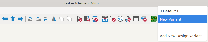
Managing variants in the Symbol Fields Table
The Symbol Fields Table provides a variant list on the left side of the dialog with buttons for common management operations:
-
Add — create a new variant (same dialog as the toolbar method).
-
Delete — remove the selected variant and all of its overrides.
-
Rename — change the name of the selected variant.
-
Copy — duplicate the selected variant under a new name, preserving all of its overrides.
-
Edit Variant Description — change the description of the selected variant. You can also edit the description of the active variant using Tools → Variants → Edit Variant Description…
| The default variant cannot be deleted, renamed, or copied. It always exists as the base design. |
Selecting a variant in the list switches the grid to display that variant’s data. Any pending edits to the previously active variant are committed automatically.
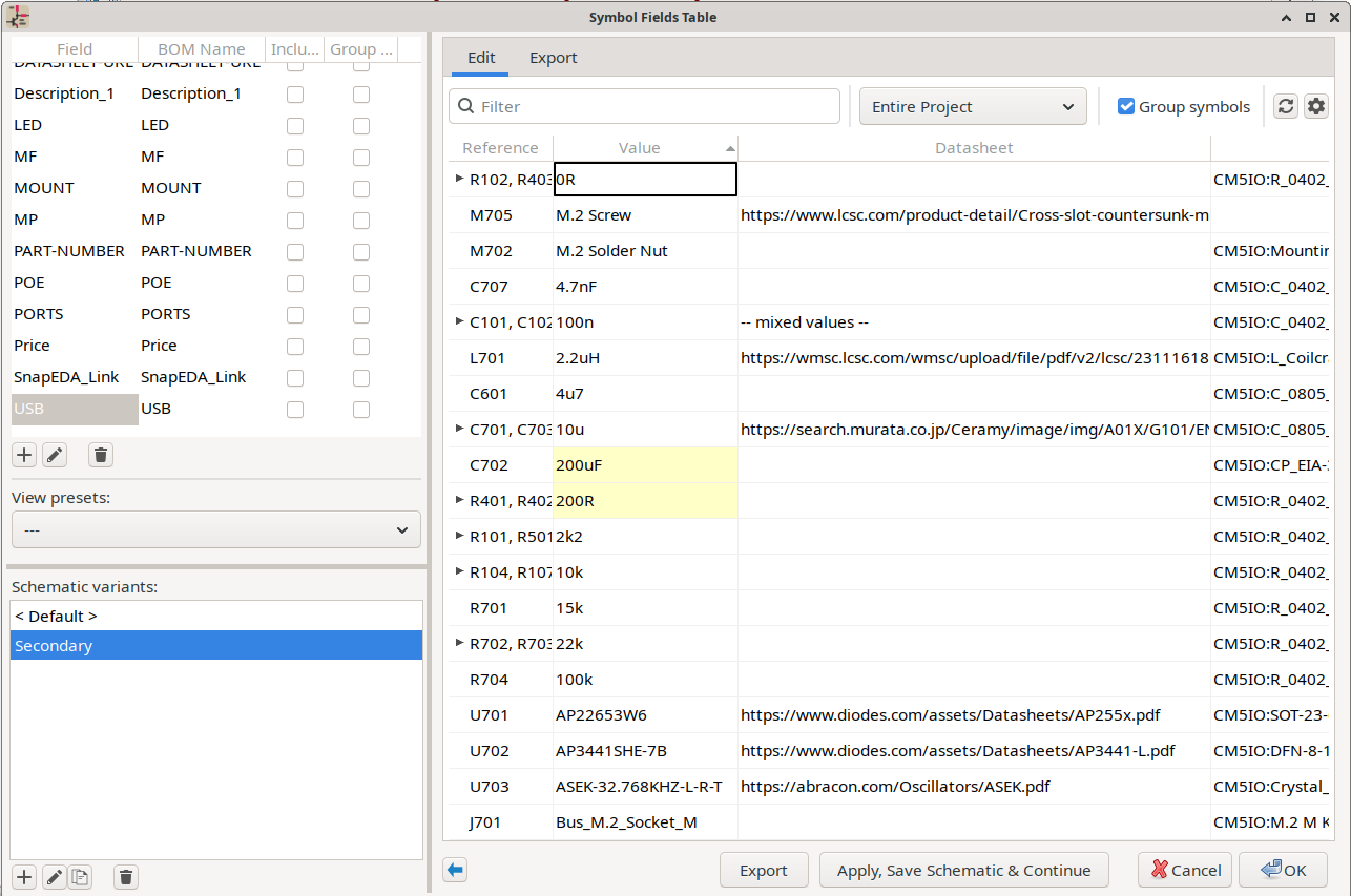
Editing variant data
When a non-default variant is selected in the toolbar, editing the schematic modifies that variant rather than the base design. Edit variant data in bulk through the Symbol Fields Table, or one symbol at a time with the normal schematic editing tools.
Editing fields in the Symbol Fields Table
The Symbol Fields Table is the primary tool for bulk-editing variant data. Select a variant from the list on the left, then edit cell values directly in the grid. The grid shows the effective value for each field in the selected variant.
Cells that differ from the default variant are highlighted with a colored background (yellow in light themes, gold in dark themes). This makes it easy to review all overrides at a glance.
To set a field back to its default value, clear the cell or set it to match the default variant’s value. The override is removed and the highlight disappears.
The same grid supports editing DNP and exclusion flags. The DNP, Exclude from BOM, Exclude from Position Files, and Exclude from Simulation columns contain checkboxes that can be toggled per variant.
Editing variants in the canvas
While a non-default variant is active, any edit made in the canvas updates that variant’s overrides. The base design is unchanged. This applies to all the normal editing tools:
-
The Properties panel on the left shows the effective field values and attribute flags for the active variant. Edits here update the variant’s overrides for the selected symbol.
-
The Symbol Properties dialog (double-click a symbol) shows the active variant name in its title bar so you know edits apply to that variant.
-
In-place field edits on the canvas and attribute changes from the right-click menu also apply to the active variant.
To mark a component as DNP for a specific variant, select the variant from the toolbar dropdown, select the symbol, and check the Do not populate checkbox in the Properties panel. The symbol is immediately drawn with an X overlay; switching back to the default variant shows the symbol without the X (assuming it is fitted in the base design). The same procedure works for the Exclude from BOM, Exclude from position files, and Exclude from simulation checkboxes.
For bulk editing across many components at once, use the Symbol Fields Table.
Generating variant-aware outputs
BOM export with variants
Open the Symbol Fields Table via Tools → Generate Bill of Materials…. The exported BOM reflects the active variant’s field values and respects its DNP and BOM exclusion flags.
To generate separate BOM files for each variant automatically, use the ${VARIANT} text variable in the output file path. For example, an output path of bom_${VARIANT}.csv produces bom_WiFi-only.csv and bom_WiFi-BT.csv when the project has those two variants defined.
Schematic plotting with variants
The Plot Schematic dialog (File → Plot…) includes a variant selector. Choose a variant to generate schematic plots that show the correct field values and DNP markings for that configuration. The default variant produces a plot of the base design.
Command-line variant support
Several sch export commands in the KiCad command-line interface support the --variant argument, including sch export bom, sch export pdf, sch export svg, sch export dxf, sch export ps, and sch export netlist. This enables scripted generation of schematic output for one or more variants.
To export a schematic PDF for a specific variant:
kicad-cli sch export pdf --variant "WiFi-only" my_project.kicad_schTo generate output for multiple variants in a single command, specify --variant more than once and use ${VARIANT} in the output path to produce separate files:
kicad-cli sch export pdf \
    --variant "WiFi-only" \
    --variant "WiFi-BT" \
    -o "schematic_${VARIANT}.pdf" \
    my_project.kicad_sch
When --variant is not specified, the default variant is used.
For a complete list of sch export commands and their variant-related options, see the Command-Line Interface reference.
Text variables
Two text variables are available for use in title blocks, text labels, and other text items:
-
${VARIANT}— resolves to the name of the currently active variant, or an empty string when the default variant is active -
${VARIANT_DESC}— resolves to the description of the currently active variant
These variables update dynamically when you switch variants and are included in plotted output, making it straightforward to identify which variant a printed schematic represents.
Transferring variants to the PCB editor
Variant data is transferred from the schematic to the PCB when you run Update PCB from Schematic (Tools → Update PCB from Schematic…). The update process synchronizes DNP flags, exclusion flags, and field overrides from each symbol to the corresponding footprint. This happens for every variant.
If a variant override has been removed in the schematic, the corresponding footprint override is reset to the base value during the update.
| Variant data flows from the schematic to the PCB, not the other way around. Always define and edit variants in the Schematic Editor, then update the PCB. |
After the update, the PCB Editor’s toolbar variant selector is populated with the same variant names. See Design variants in the PCB Editor manual for details on working with variants in the board layout.
Symbols and Symbol Libraries
KiCad organizes symbols into symbol libraries, which hold collections of symbols. Each symbol in a schematic is uniquely identified by a full name that is composed of a library nickname and a symbol name. For example, the identifier Audio:AD1853 refers to the AD1853 symbol in the Audio library.
Managing symbol libraries
KiCad uses a table of symbol libraries to map a symbol library nickname to an underlying symbol library on disk. Kicad uses a global symbol library table as well as a table specific to each project. Libraries are not loaded unless they are included in either the global or project-specific library table.
To edit either symbol library table, use Preferences → Manage Symbol Libraries….
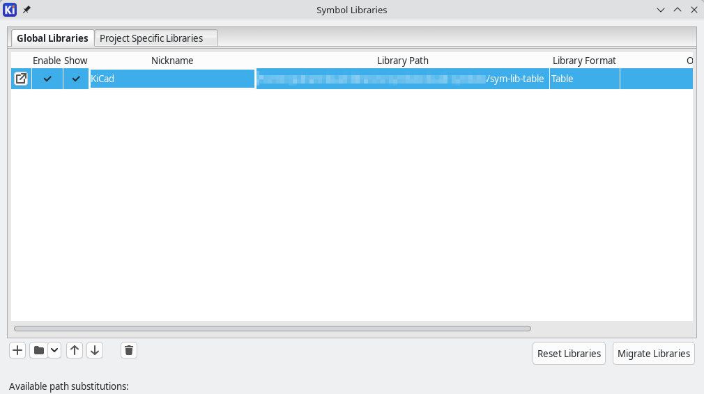
The global symbol library table contains the list of libraries that are always available regardless of the currently loaded project. The table is saved in the file sym-lib-table in the KiCad configuration folder. The location of this folder depends on the operating system being used.
The project specific symbol library table contains the list of libraries that are available specifically for the currently loaded project. If there are any project-specific symbol libraries, the table is saved in the file sym-lib-table in the project folder.
Many (or even all) of the loaded libraries may be contained in a nested library table, as shown in the screenshot above. To expand a nested library table and view its contents, press the ![]() button next to the nested library table entry. This opens the nested table in a new tab, as shown below.
button next to the nested library table entry. This opens the nested table in a new tab, as shown below.
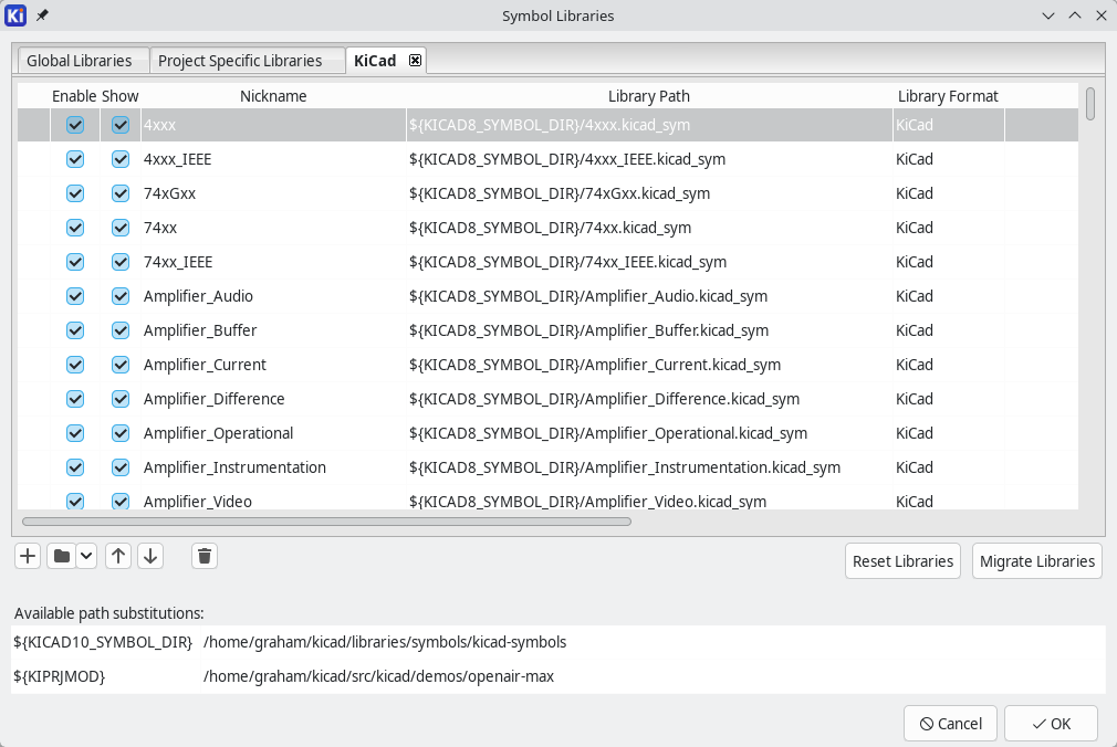
KiCad’s symbol library management system allows directly using many types of symbol libraries, including formats that are native to other non-KiCad EDA tools:
-
KiCad symbol libraries (
.kicad_symfiles, or folders of.kicad_symfiles) -
KiCad Legacy symbol libraries (
.libfiles) -
Altium Designer libraries (
.SchLibor.IntLibfiles) -
CADSTAR Schematic Archive libraries (
.libfiles) -
KiCad database library configuration files (
.kicad_dblfiles) -
Eagle libraries (
.xmlfiles) -
EasyEDA (JLCEDA) Standard Edition libraries (
.jsonfiles) -
EasyEDA (JLCEDA) Professional Edition libraries (
.elibz,.epro, or.zipfiles) -
KiCad HTTP library configuration files (
.kicad_httplibfiles)
Non-KiCad symbol libraries, including KiCad Legacy symbol libraries, can be migrated to KiCad .kicad_sym format using the Migrate Libraries button (see the migrating libraries section).
KiCad only supports writing to KiCad’s native .kicad_sym format symbol libraries. All other symbol library formats are read-only. To modify a non-KiCad format symbol library, you must first convert it to KiCad format.
|
Library tables can also include other library tables, which are called nested library tables. When a nested library table is used, the libraries in the nested table are loaded as if they were included directly in the main table.
Initial configuration
The first time KiCad runs (or any time KiCad runs and no configuration is found), KiCad will guide you through creating a new configuration or importing a configuration from a previous version. This includes setting up a new footprint library table. This process is described in the Project Manager documentation.
You can reset your footprint library table to the default by clicking the Reset Libraries button in the footprint library table dialog.
| Resetting your footprint library table will permanently change your footprint library table on disk. |
The default symbol library table contains a single entry, which points to another symbol library table containing all of KiCad’s default symbol libraries. This nested library table is maintained as part of the KiCad libraries and is updated along with KiCad and its libraries. You should not edit it yourself.
| KiCad’s default symbol libraries are included in your library table via a nested library. This allows the list of default KiCad libraries to be updated when KiCad and its libraries are updated, without affecting your personal library configuration. Your personal library table configuration can be maintained between KiCad versions, while still allowing you to receive updates to the default libraries. |
Managing table entries
Symbol libraries can only be used if they have been added to either the global or project-specific symbol library table (or to a nested table included in either top-level table).
Add a library either by clicking the ![]() button and selecting a library or clicking the
button and selecting a library or clicking the ![]() button and typing the path to a library file. The selected library will be added to the currently opened library table (Global or Project Specific). Libraries can be removed by selecting desired library entries and clicking the
button and typing the path to a library file. The selected library will be added to the currently opened library table (Global or Project Specific). Libraries can be removed by selecting desired library entries and clicking the ![]() button.
button.
When an entry in the library table is itself another library table, you can open this nested table by clicking the ![]() button next to the nested table’s entry. This opens the nested table in a new tab, where you can see and edit the libraries included in the nested table. To add a nested library table, click the downwards arrow next to the
button next to the nested table’s entry. This opens the nested table in a new tab, where you can see and edit the libraries included in the nested table. To add a nested library table, click the downwards arrow next to the ![]() button, choose the Table library type, then browse to the table file.
button, choose the Table library type, then browse to the table file.
The ![]() and
and ![]() buttons move the selected library up and down in the library table. This does not affect the display order of libraries in the Symbol Editor or Symbol Chooser.
buttons move the selected library up and down in the library table. This does not affect the display order of libraries in the Symbol Editor or Symbol Chooser.
Libraries can be disabled by unchecking the Enable checkbox in the first column. Inactive libraries are still in the library table but do not appear in any library browsers and are not loaded from disk, which can reduce loading times. Alternatively, you can hide a library from the library browsers while still loading it from disk by unchecking the Show checkbox.
| Hiding a library is primarily useful in conjunction with database libraries. Database libraries define symbols by adding metadata to symbol definitions from another symbol library. This base symbol library needs to be loaded, so it cannot be disabled, but for convenience the library can be hidden if it is not needed beyond the database library definition. |
A range of libraries can be selected by clicking the first library in the range and then Shift-clicking the last library in the range.
Each library must have a unique nickname: duplicate library nicknames are not allowed in the same table. However, nicknames can be duplicated between the global and project library tables. Libraries in the project table take precedence over libraries with the same name in the global table.
Library nicknames do not have to be related to the library filename or path. The colon character (:) cannot be used in library nicknames or symbol names because it is used as a separator between nicknames and symbols.
Each library entry must have a valid path. Paths can be defined as absolute, relative, or by path variable substitution.
The appropriate library format must be selected in order for the library to be properly read. The supported formats are listed above. Only KiCad format libraries (.kicad_sym) can be saved. Other symbol library formats are read-only and must be converted to KiCad format before you can modify them.
There is an optional description field to add a description of the library entry. The option field is not used at this time so adding options will have no effect when loading libraries.
Nested library tables
In addition to containing libraries, library tables can also contain other library tables. Library tables that are referenced by other library tables in this way are called nested library tables. Any libraries in a nested library table are loaded as if they were directly listed in the top-level library table.
Nested library tables let you separate groups of libraries into different library table files, then include all of the individual tables into the main top-level library table. This could be used, for example, to make a standard library table for your company, and share that table with everyone who needs it. Each user can then access the standard set of company libraries after they add the shared table as a nested library table in their own global table.
When KiCad is configured to its default library table configuration, the global library table contains a single entry, which is a nested library table. This nested table is part of KiCad’s default libraries and lists all of the KiCad default symbol libraries. When KiCad is updated, this nested table is also updated, which allows you to receive an updated list of KiCad’s default libraries without disturbing your personal library configuration.
Path variable substitution
The symbol library tables support path variable substitution, which allows you to define path variables containing custom paths to where your libraries are stored. Path variable substitution is supported by using the syntax ${PATH_VAR_NAME} in the symbol library path.
By default, KiCad defines several path variables which are described in the project manager documentation. Path variables can be configured in the Preferences → Configure Paths… dialog.
Using path variables in the symbol library tables allows libraries to be relocated without breaking the symbol library tables, so long as the path variables are updated when the library location changes.
KiCad will automatically resolve versioned path variables from
older versions of KiCad to the value of the corresponding variable from
the current KiCad version, as long as the old variable is not explicitly
defined itself. For example, ${KICAD9_SYMBOL_DIR} will
automatically resolve to the value of ${KICAD10_SYMBOL_DIR} if there
is no KICAD9_SYMBOL_DIR variable defined.
|
${KIPRJMOD} is a special path variable that always expands to the absolute path of the current project directory. ${KIPRJMOD} allows libraries to be stored in the project folder without having to use an absolute path in the project library table. This makes it possible to relocate projects without breaking their project library tables.
Usage patterns
Symbol libraries can be defined either globally or specifically to the currently loaded project. Symbol libraries defined in the user’s global table are always available and are stored in the sym-lib-table file in the user’s KiCad configuration folder. The project-specific symbol library table is active only for the currently open project file.
There are advantages and disadvantages to each method. Defining all libraries in the global table means they will always be available when needed. The disadvantage of this is that load time will increase.
Defining all symbol libraries on a project specific basis means that you only have the libraries required for the project which decreases symbol library load times. The disadvantage is that you always have to remember to add each symbol library that you need for every project.
One usage pattern would be to define commonly used libraries globally and the libraries only required for the project in the project specific library table. There is no restriction on how to define libraries.
Migrating symbol libraries to KiCad format
Non-KiCad format libraries, including legacy libraries (.lib files), are read-only. They need to be converted to KiCad format (.kicad_sym files) before you can save changes to them.
| As with most KiCad files, newer versions of KiCad can open older-format library files, but older versions of KiCad cannot read files once they have been saved by a newer version of KiCad. |
Libraries in other formats can be converted to KiCad libraries by selecting them in the symbol library table and clicking the Migrate Libraries button. Multiple libraries can be selected and migrated at once by Ctrl-clicking or shift-clicking.
Libraries can also be converted one at a time by opening them in the Symbol Editor and saving them as a new library.
Unpacked libraries
A KiCad symbol library is typically in the form of a single .kicad_sym file that contains multiple symbols. This is known as a packed library, in the sense that multiple symbols are packed into a single file.
Beginning in KiCad 10.0, symbol libraries can also take the form of a folder containing multiple .kicad_sym files, with each file containing one or more symbols. The folder and the .kicad_sym files in it comprise a single symbol library, but each .kicad_sym file is otherwise in the same format as a packed library. This is known as an unpacked library.
By convention, unpacked symbol libraries use the .kicad_symdir "extension" on the folder name, but this is not required.
| Unpacked libraries have the same structure as footprint libraries. A folder represents the library, and the files inside are the contents of the library. |
In most cases, packed libraries are preferred because they offer greater performance for libraries with many symbols. Unpacked libraries may be more convenient, however, if multiple people may be editing a symbol library at the same time, as the multiple-file structure avoids multiple conflicting edits to the same file.
Legacy project remapping
When loading a schematic created prior to the symbol library table implementation, KiCad will attempt to remap the symbol library links in the schematic to the appropriate library table symbols. The success of this process is dependent on several factors:
-
the original libraries used in the schematic are still available and unchanged from when the symbol was added to the schematic.
-
all rescue operations were performed when detected to create a rescue library or keep the existing rescue library up to date.
-
the integrity of the project symbol cache library has not been corrupted.
|
The remapping will make a back up of all the files that are changed during remapping in the rescue-backup folder in the project folder. Always make a back up of your project before remapping just in case something goes wrong. |
|
The rescue operation is performed even if it has been disabled to ensure the correct symbols are available for remapping. Do not cancel this operation or the remapping will fail to correctly remap schematics symbols. Any broken symbol links will have to be fixed manually. |
|
If the original libraries have been removed and the rescue was not performed, the cache library can be used as a recovery library as a last resort. Copy the cache library to a new file name and add the new library file to the top of the library list using a version of KiCad prior to the symbol library table implementation. |
Browsing symbol libraries
The Symbol Library Browser allows you to quickly examine the contents of symbol libraries. The Symbol Library Viewer can be accessed by clicking ![]() icon on the main Symbol Editor toolbar or with View → Symbol Library Browser.
icon on the main Symbol Editor toolbar or with View → Symbol Library Browser.
To examine the contents of a library, select a library from the list in the left hand panel. All symbols in the selected library will appear in the second panel. Select a symbol name to view the symbol.
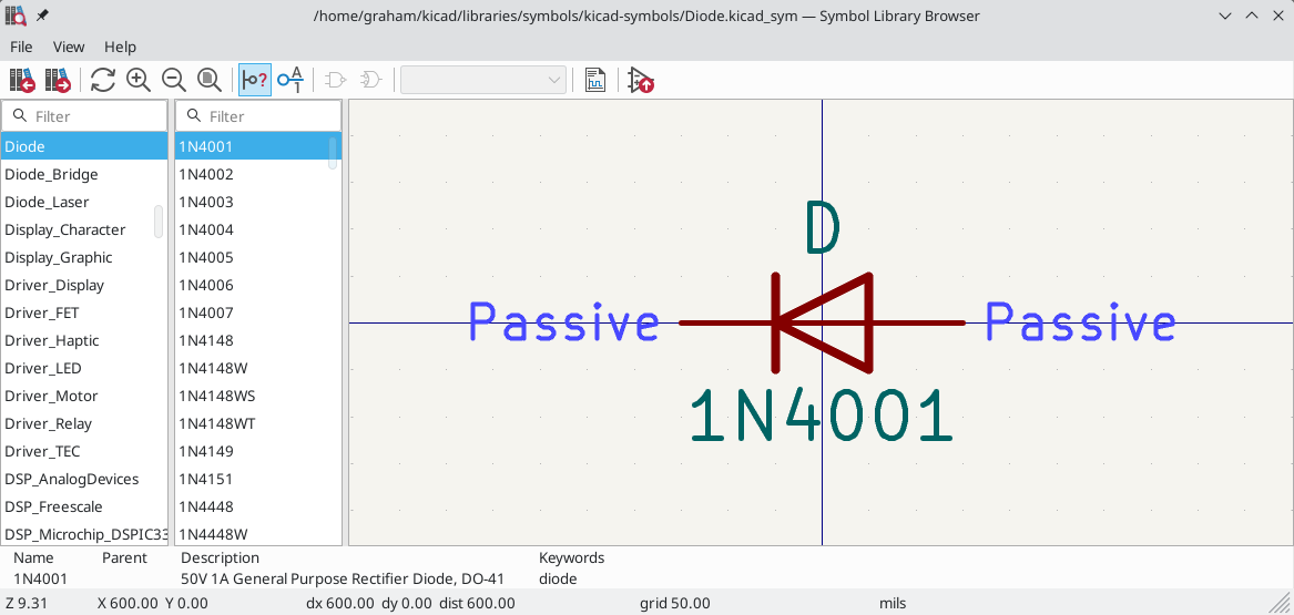
Double clicking the name of a symbol or using the ![]() button adds the symbol to the schematic.
button adds the symbol to the schematic.
The top toolbar contains the following commands:
|
Select previous symbol in library. |
|
Select next symbol in library. |
|
Zoom tools. |
|
Toggle display of pin electrical types. |
|
Toggle display of pin numbers. |
|
Select the body style of a symbol with multiple body styles. |
|
Select the unit of a multi-unit symbol. |
|
Open the symbol’s datasheet, if it is defined. |
|
Insert current symbol into the schematic. |
Creating and editing symbols
A symbol is a schematic representation of a component. A symbol is composed of:
-
Graphical items (lines, circles, arcs, text, etc.) that determine how symbol looks in a schematic.
-
Pins, which connect to wires in the schematic and correspond to footprint pads in the PCB. Pins have both graphic properties (line, clock, inverted, low level active, etc.) and electrical properties (input, output, bidirectional, etc.) used by the Electrical Rules Check (ERC) tool.
-
Fields, such as references, values, corresponding footprint names for PCB design, etc.
A symbol library is composed of one or more symbols. Generally the symbols are logically grouped by function, type, and/or manufacturer. Each symbol library is a single file with the .kicad_sym extension.
Symbols can be derived from another symbol in the same library. Derived symbols share the basic shape and pin definitions of a base symbol, but can override the base symbol’s metadata. For more information, see the derived symbol section.
Symbol Editor overview
KiCad provides a symbol editing tool that allows you to create libraries; add, edit, delete, or transfer symbols between libraries; export symbols to files; and import symbols from files. The Symbol Editor can be launched from the KiCad Project Manager or from the Schematic Editor (Tools → Symbol Editor). You can also open the Symbol Editor from the a symbol in the schematic; in this way you can edit either the library copy or the schematic copy of that symbol in the editor.
| Editing the library version of a symbol will not affect any copies of that symbol that have been added to a schematic until the schematic copy is updated from the library. Conversely, editing the schematic version of a symbol will not affect the library version of a symbol or any other copies of that symbol in a schematic. |
In general, the flow for designing a symbol involves:
-
Defining if the symbol is made up of one or more units.
-
Defining if the symbol has an alternate body style (also known as a De Morgan representation).
-
Diseñar su representación simbólica usando líneas, rectángulos, círculos, polígonos y texto.
-
Adding pins by carefully defining each pin’s graphical elements, name, number, and electrical property (input, output, tri-state, power output, etc.).
-
Determining if the symbol should be derived from another symbol with the same graphical design and pin definition.
-
Añadir campos opcionales como nombre de la huella usada por el programa de diseño de PCB y/o definiendo su visibilidad.
-
Documenting the symbol by adding a description string and links to data sheets, etc.
-
Salvar el componente en la biblioteca deseada.
The Symbol Editor main window is shown below. It has three toolbars for quick access to common features and a symbol viewing/editing canvas. Not all commands are available on the toolbars, but all commands are available in the menus.
| You can edit the toolbars' contents in the Toolbar page of the Symbol Editor Preferences. |
In addition to the toolbars, there are collapsible panels for the symbol tree, Properties Manager, and selection filter on the left. The bottom of the window contains a message panel that shows details about the selected object.
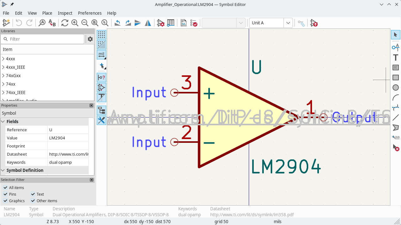
Top toolbar
The main toolbar is at the top of the main window. It has buttons for the undo/redo commands, zoom commands, symbol properties dialogs, and unit/representation management controls.
|
Create a new symbol in the selected library. |
|
Save the currently selected library. All modified symbols in the library will be saved. |
|
Undo last edit. |
|
Redo last undo. |
|
Refresh display. |
|
Zoom in. |
|
Zoom out. |
|
Zoom to fit symbol in display. |
|
Zoom to fit selection. |
|
Rotate counter-clockwise. |
|
Rotate clockwise. |
|
Mirror horizontally. |
|
Mirror vertically. |
|
Edit the current symbol’s properties. |
|
Edit the symbol’s pins in a tabular interface. |
|
Open the symbol’s datasheet, if it is defined. |
|
Run the symbol checker to test the current symbol for design errors. |
|
Select the body style to display. The drop down control will be disabled if the current symbol does not have multiple body styles. |
|
Select the unit of a multi-unit symbol to display. The drop down control will be disabled if the current symbol does not have multiple units. |
|
Enable synchronized pin edit mode. When this mode is enabled, any pin modifications are propagated to all other symbol units. Pin number changes are not propagated. This mode is automatically enabled for symbols with multiple interchangeable units and cannot be enabled for symbols with only one unit. |
|
Insert current symbol into the schematic. |
Left toolbar display controls
The left toolbar provides options to change the display of items in the Symbol Editor.
|
Toggle grid visibility on and off. |
|
Toggle item-specific grid overrides on and off. |
|
Set units to inches, mils (0.001 inch), or millimeters. Clicking the button toggles to the next unit, or you can choose a unit directly by expanding the palette (click and hold/drag). |
|
Switches the cursor crosshair between small, fullscreen, and 45-degree-rotated fullscreen. Clicking the button toggles to the next crosshair type, or you can choose a crosshair directly by expanding the palette (click and hold/drag). |
|
Toggle display of pin electrical types. |
|
Toggle display of hidden (invisible) pins. |
|
Toggle display of hidden (invisible) fields. |
|
Toggle display of library and symbol tree. |
|
Toggle display of Properties Manager panel. |
Right toolbar tools
Placement and drawing tools are located in the right toolbar.
|
Select tool. Right-clicking with the select tool opens the context menu for the object under the cursor. Left-clicking with the select tool displays the attributes of the object under the cursor in the message panel at the bottom of the main window. Double-left-clicking with the select tool will open the properties dialog for the object under the cursor. |
|
Pin tool. Left-click to add a new pin. |
|
Graphical text tool. Left-click to add a new graphical text item. |
|
Graphical textbox tool. Left-click to add a new graphical textbox item. |
|
Rectangle tool. Left-click to begin drawing the first corner of a graphical rectangle. Left-click again to place the opposite corner of the rectangle. |
|
Circle tool. Left-click to begin drawing a new graphical circle from the center. Left-click again to define the radius of the circle. |
|
Arc tool. Left-click to begin drawing a new graphical arc item from the first arc end point. Left-click again to define the second arc end point. Adjust the radius by dragging the arc center point. |
|
Bezier curve tool. Left-click to begin drawing a new graphical bezier curve item. First click for the start point, then for the control points and the end point. Adjust the curve by dragging the points. |
|
Connected line tool. Left-click to begin drawing a new graphical line item in the current symbol. Left-click for each additional connected line. Double-left-click to complete the line. |
|
Connected line tool. Left-click to begin drawing a new graphical line item in the current symbol. Left-click for each additional connected line. Double-left-click to complete the line. |
|
Anchor tool. Left-click to set the anchor position of the symbol. |
|
Delete tool. Left-click to delete an object from the current symbol. |
Browsing, modifying, and saving symbols
The ![]() button displays or hides the list of available libraries, which allows you to select an active library. When a new symbol is created, it will be placed in the active library.
button displays or hides the list of available libraries, which allows you to select an active library. When a new symbol is created, it will be placed in the active library.
Clicking on a symbol name opens that symbol in the editor, and hovering the cursor over the name of a symbol displays a preview of the symbol.
| Some symbols are derived from other symbols. Derived symbol names are displayed in italics in the treeview. If a derived symbol is opened, its symbol graphics will not be editable. Its symbol fields will be editable as normal. To edit the graphics of a base symbol and all of its derived symbols, open the base symbol. |
After modification, a symbol can be saved in the current library or a different library. To save the modified symbol in the current library, click the ![]() icon.
icon.
| Saving a modified symbol also saves all other modified symbols in the same library. |
To save the symbol changes to a new symbol, click File → Save As…. The symbol can be saved in the current library or a different library (including a new library), and a new name can be set for the symbol. Alternatively, you can use File → Save Copy As…, which behaves the same as Save As except that the original symbol remains open rather than switching to the new symbol.
To create a new file containing only the current symbol, click File → Export → Symbol…. This file will be a standard symbol library file which will contain only one symbol. The library will not be added to your library table.
The editor can also open symbols from the schematic. To edit a symbol from the schematic, right click a symbol in the Schematic Editor and select Open in Schematic Editor (Ctrl+E).
Editing and saving the schematic copy of a symbol will only update that symbol in the schematic; it will not update other copies of that symbol in the schematic, and it will not change the original library copy of the symbol. When you open the schematic copy of a symbol, the Schematic Editor displays an info bar that warns you the library copy will not be modified. You can click the link in this info bar to open the library version of the symbol instead, or press Ctrl+Shift+E.
Creating a new symbol library
You can create a new symbol library by clicking File → New Library…. This opens a file browser for you to choose a location and name for the new library. Symbol libraries are saved as a file; the file name is the library name plus the suffix .kicad_sym.
The file browser also lets you choose whether the new library should be added to the global symbol library table or the project symbol library table. Libraries in the global library table will be available to all projects, while libraries in the project library table will only be available in the current project.
| The global and project symbol library tables are managed using Preferences → Manage Symbol Libraries…. This includes deleting and renaming symbol libraries. For more information about managing library tables, see the symbol library table documentation. |
After choosing a name, location, and library table, a new, empty library is created. When you create new symbols, you can save them in this library.
Creating a new symbol
To create a new symbol in the current symbol library, click the ![]() button. You will be asked for a number of symbol properties.
button. You will be asked for a number of symbol properties.
-
A symbol name.
-
An optional base symbol to derive the new symbol from. The new symbol will use the base symbol’s graphical shape and pin configuration, but other symbol information can be modified in the derived symbol. The base symbol must be in the same library as the new derived symbol.
-
The reference designator prefix (
U,C,R…). -
The number of units per package, and whether those units are interchangeable (for example a 7400 quad NAND symbol could have 4 units, one for each gate).
-
If an alternate body style (sometimes referred to as a "De Morgan equivalent") is desired.
-
Whether the symbol is a power symbol. Power symbols appear in the Add Power Symbol dialog in the Schematic editor, make global net connections based on their value, cannot be assigned a footprint, and are excluded from the PCB and bill of materials.
-
Whether the symbol should be excluded from the bill of materials.
-
Whether the symbol should be excluded from the PCB.
There are also several graphical options.
-
The offset between the end of each pin and its pin name.
-
Whether the pin number and pin name should be displayed.
-
Whether the pin names should be displayed alongside the pins or at the ends of the pins inside the symbol body.
These properties can also be changed later in the Symbol Properties window.
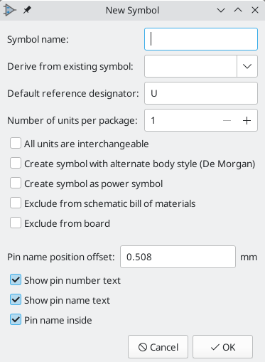
A new symbol will be created in the selected library using the given properties. The new symbol is opened in the editor.
The blue cross in the center is the symbol anchor, which specifies the symbol origin i.e. the coordinates (0, 0). The anchor can be repositioned by selecting the ![]() button and clicking on the new desired anchor position.
button and clicking on the new desired anchor position.
Editing symbol properties
Symbols have a number of properties and metadata items that can be defined. These include text fields, attributes that can be set or not (such as Do Not Populate), pin connection settings, and filters for appropriate footprints. These are initially defined in the library copy of the symbol, but they can be modified on a per-instance basis once a symbol is added to a schematic. In other words, two copies of the same symbol in a single schematic can have their properties edited separately.
To change the symbol properties, click on the ![]() button to show the Symbol Properties dialog. You can also double click an empty spot in the editing canvas.
button to show the Symbol Properties dialog. You can also double click an empty spot in the editing canvas.
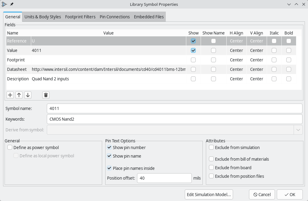
The most important settings are in the General tab. Here you can edit symbol fields as well as many basic properties for the symbol. Other tabs contain options for multiple units and body styles, footprint filters, jumper pins, and embedded files.
Symbol fields are explained in a separate section. The other settings in the general tab are:
-
Symbol name is the symbol’s name in the library. Symbols are identified by a combination of the library and symbol name. In older versions of KiCad, the symbol name was linked to the
Valuefield. This link is removed in KiCad 7.0 and later. -
The keywords should contain additional terms related to the component. Keywords are primarily used, in combination with the symbol name and the
Descriptionfield, for searching for the symbol in the Symbol Chooser and the Symbol Editor. Those three items are also displayed when you select a symbol in the Symbol Chooser. -
Define as power symbol and Define as local power symbol control whether the symbol acts as a power symbol, making connections between otherwise separate nets.
-
The graphic options Show pin number and Show pin name control the visibility of the pin number and pin name text.
-
Place pin names inside controls the pin name position relative to the pin body. The pin names will be displayed inside the symbol outline if the option is checked. In this case the Pin Name Position Offset property defines the shift of the text away from the body end of the pin. A value from
0.02to0.05inches is usually reasonable. -
Exclude from simulation, Exclude from bill of materials, Exclude from board, and Exclude from position files set the default state of these symbol attributes when the symbol is added to the schematic.
The example below shows a symbol with the Place pin name inside option unchecked. Notice the position of the names and pin numbers.
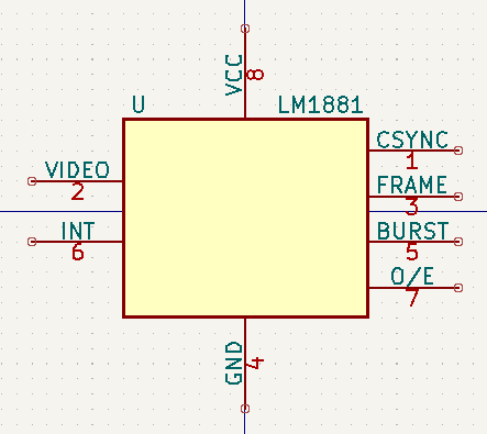
Symbol units and alternate body styles
Symbols can have more than one unit per package, each with different graphics and pin configurations. This is often used for logic gates, opamps, or other components that have multiple subunits within one physical package. Each symbol unit can be placed separately in the schematic, which can make it easier to draw neat schematics.
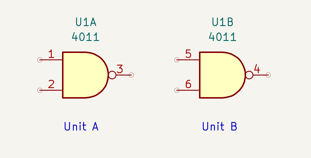
Symbols can also have multiple body styles, which are alternate graphical representations of the same symbol. For example, the symbol for a NAND gate could have one body style showing an ANSI-style AND gate with inverting "bubble" on the output, another body style drawn as an OR gate with inverting "bubbles" on the inputs, and a third body style with an IEC-style rectangular NAND gate symbol.
| Before KiCad 10.0, a maximum of one alternate body style per symbol was possible, and a symbol’s alternate body style was sometimes referred to as a "De Morgan equivalent". Beginning in KiCad 10.0, multiple alternate body styles are possible. |
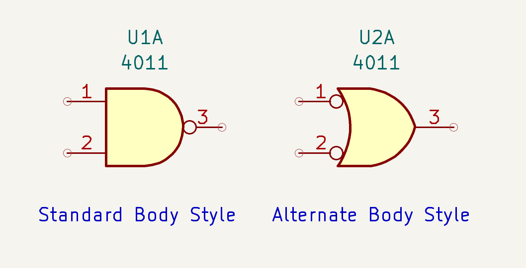
By default, pins are part of a single unit and body style in the symbol. Alternatively, pins can be set as common to all units or common to all body styles. When a pin is common to all units or all body styles, it only needs to be created once, no matter how many units or body styles are used. Graphics and text may also be set as common to all units or body styles, but typically graphics are specific to a single body style so that each body style can have a unique appearance.
The settings for adjusting a symbol’s units and body styles are in the Units & Body Styles tab of the Symbol Properties dialog.
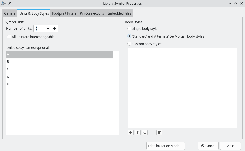
-
Number of Units controls the number of symbol units.
-
All units are interchangeable should be set if all symbol units are equivalent. If all units are interchangeable, you can use the Synchronized Pin Edits mode to quickly make changes to all units.
-
The Unit Display Names table lets you set an optional name for each unit. If you do not configure display names, symbol units are named
Unit A,Unit B, etc. -
The Body Styles options let you select between a single body style, two body styles for traditional "Standard" and "De Morgan" representations of a symbol, and an arbitrary number of custom body styles. If you enable custom body styles, you can set the name for each style.
You can only view and edit one symbol unit and body style at a time in the symbol editor’s editing canvas. Use the  unit selection dropdown to select the unit you wish to edit, and use the
  body style selection dropdown to select a body style.
|
Synchronized Pins Edit Mode can be enabled by clicking the
|
Symbol graphics
Graphical elements create the visual representation of a symbol and contain no electrical connection information. You can draw new graphic shapes using the buttons on the right toolbar. The following types of objects are available:
-
Lines (
 ) and polygons (
 ) defined by start and end points.
 -
Rectangles (
 ) defined by two diagonal corners.
 -
Circles (
 ) defined by the center and radius.
 -
Arcs (
 ) defined by the starting and ending point of the arc and its center.
 -
Graphical text (
 ) and textboxes (
 ), which is automatically oriented to be readable, even when the symbol is mirrored. Note that graphic text items are not the same as symbol fields.
Each graphic item (line, arc, circle, etc.) can be defined as common to all units and/or body styles or specific to a given unit and/or body style.
Element options can be quickly accessed by right-clicking on the element to display the context menu for the selected element. You can also double-left-click on an element to modify its properties, or edit its properties using the Properties Manager panel.
Below is the properties dialog for a polygon element.
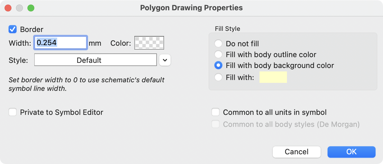
Las propiedades de un elemento gráfico son:
-
Border determines whether the the shape’s outline should be drawn.
-
Width and color define the line width and color of the border. A border width of
0uses the schematic’s default symbol line width. Style determines the line style of the border (solid, dashed, dotted, etc.). -
Fill Style determines if the shape defined by the graphical element is to be drawn unfilled or filled. The fill color can be the color theme’s body outline color, body background color, or a custom color.
-
Common to all units in symbol determines if the graphical element is drawn for each unit in symbol with more than one unit per package or if the graphical element is only drawn for the current unit.
-
Common to all body styles determines if the graphical element is drawn for each symbolic representation in symbols with an alternate body style or if the graphical element is only drawn for the current body style.
-
Private to Symbol Editor causes the shape to be visible only when the symbol is edited in the Symbol Editor. The shape will be hidden when the symbol is added to a schematic.
Symbol pins
Symbol pins are the parts of a symbol that connect to wires in the schematic. Each symbol pin corresponds to a footprint pad in the PCB, and pins are matched to pads by number, so each pin’s number must match the corresponding pad number in the footprint.
You can create and insert a pin by clicking on the ![]() button. This opens the Pin Properties dialog, then allows you to place the pin in the symbol. After placing a pin, you can edit its properties by reopening its Properties dialog (E or double click on the pin) or by using the Properties Manager.
button. This opens the Pin Properties dialog, then allows you to place the pin in the symbol. After placing a pin, you can edit its properties by reopening its Properties dialog (E or double click on the pin) or by using the Properties Manager.
| You can edit all of a symbol’s pins at once using the Pin Table. This may be a more convenient way to edit pins, especially for symbols with many pins. |
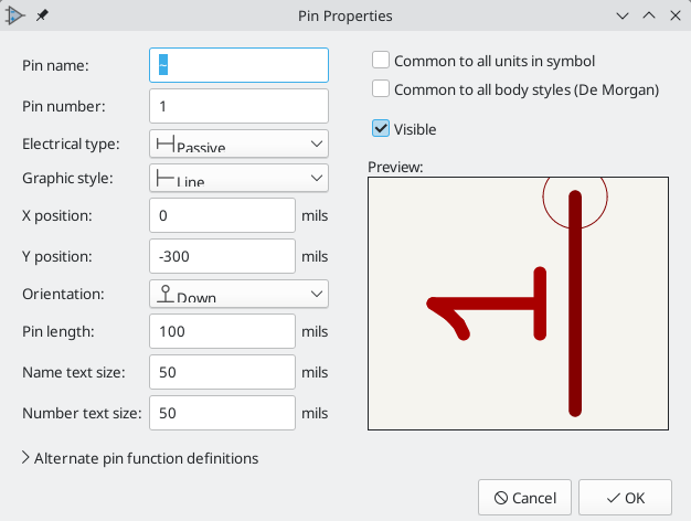
Pins have the following properties:
-
Pin name is an optional name for the pin. Pin names can be displayed as part of the symbol, and if present they are used as part of automatically generated net names for unnamed nets attached to the pin. Pin names cannot contain spaces; any spaces in a pin name are automatically replaced with underscores. To define a pin name with an inverted signal (overbar) use the
~(tilde) character followed by the text to invert in braces. For example,~{FO}Owould display FO O. -
Pin number is a string that uniquely identifies the pin. Symbol pins are matched to footprint pads by pin/pad number, so pin numbers should correspond to pad numbers. Pin numbers are typically unique within a symbol. In addition to numbers, pin numbers can contain letters or symbols. Pin numbers cannot contain spaces; any spaces in a pin number are automatically replaced with underscores.
-
Electrical type describes how the pin behaves electrically, such as input, output, or open collector. Electrical types affect ERC and some other behavior.
-
Graphic style controls the appearance of the pin, such as an inverted pin or a clock input, but does not have any other effects.
-
X position and Y position are the location of the pin relative to the symbol’s anchor.
-
Orientation is the direction the pin extends (left, right, up, or down) relative to its wire attachment point.
-
Pin length is the length of the pin.
-
Name text size and Number text size are the size that the pin name and number, respectively, are displayed at.
-
Common to all units in symbol controls whether the pin is part of all symbol units or only the currently active symbol unit.
-
Common to all body styles controls whether the pin is shown in all body styles or only the currently active body style.
-
Visible controls whether the pin is shown or hidden. Note that hidden power input pins have special behavior.
-
Alternate pin definitions are optional additional combinations of pin name, electrical type, and graphic style that can be selected in the schematic instead of the default pin definition. These can be used, for example, to represent selectable pin functions in a microcontroller.
Pin electrical types
Each pin in a symbol has an electrical type, such as input, output, or tri-state.
Choosing the correct electrical type is important for the schematic ERC tool. ERC will check that pins are connected appropriately, for example ensuring that input pins are driven and power inputs receive power from an appropriate source.
You can use the Pin Conflicts Map in the schematic editor to configure which pin types are allowed to connect and which will conflict. The default Pin Conflicts settings are briefly explained below. For more information, see the ERC documentation.
Additionally, some pin types have special behavior outside of ERC. In the router, pads corresponding to a free pin can be connected to copper of any other net without causing a DRC error, and multiple pads corresponding to a single unconnected pin do not need to be connected to each other in the board.
| The pin type that produces the optimal ERC pin conflict checking behavior is not always the same as the pin’s conceptual pin type. When selecting a pin type, you should consider how that type will interact with the pin type of other connected pins and whether that will result in the desired ERC behavior. An example is an analog control pin that generates a current and senses the voltage generated by that current flowing through an external resistor. This pin could be considered an input pin because it senses a voltage provided externally. However, in a schematic this pin will be connected to a resistor pin (passive) and not to an output pin. There shouldn’t be an ERC violation if the pin isn’t connected to an output pin; in fact, there should be an ERC violation if the pin does connect to another output pin, as the pin would be sourcing a current on a net that is already driven. Therefore such a pin should have the Output pin type even though it is sensing a voltage and could be considered an input. |
Pin Type |
Descripción |
Input |
A pin which is exclusively an input. The default Pin Conflicts settings allow input pins to connect to most other types of pin. Also, an ERC violation will be produced if an input pin is not driven, i.e. it is not connected to a pin with type output, bidirectional, tristate, power output, or passive. |
Output |
A pin which is exclusively an output. The default Pin Conflicts settings allow output pins to connect to most types of pin that aren’t also outputs. |
Bidirectional |
A pin that can be either an input or an output, such as a microcontroller data bus pin. The default Pin Conflicts settings allow bidirectional pins to connect to most other types of pins, though there are a few more restrictions than with input pins. |
Tri-state |
A three state output pin (high, low, or high impedance). The default Pin Conflicts settings allow tri-state pins to connect to most other types of pins, but warnings are generated when they are connected to most types of output or power pins. |
Pasivo |
A pin that is not connected to active electronics, for example pins on a resistor or connector. The default Pin Conflicts settings allow passive pins to connect to most other types of pin. |
Free |
A pin that does not electrically affect the operation of the device. These pins typically represent package leads that are not internally connected to the chip. The default Pin Conflicts settings allow free pins to connect to most other types of pin. In the PCB editor, pads corresponding to free pins can be connected to copper of any other net without causing a DRC error. |
Unspecified |
A pin which has an unspecified type. With the default Pin Conflicts settings, ERC generates warnings when unspecified pins are connected to most other types of pins. |
Power input |
A pin that powers the device. The default Pin Conflicts settings allow power input pins to connect to most other pin types. However, power input pins that are not connected to a power output pin generate an ERC violation. Additionally, power input pins that are marked invisible are automatically connected to the net with the same name as the pin. This behavior is supported primarily for legacy projects and is not recommended for new designs. See the Hidden Power Pin section for more information. |
Power output |
A pin that provides power to other pins, such as a regulator output. The default Pin Conflicts settings allow power output pins to connect to most types of input pins, but not output pins. |
Open collector |
An open collector logic output. The default Pin Conflicts settings allow open collector pins to connect to most input pins and other open collector pins, but not to most other types of outputs. |
Open emitter |
An open emitter logic output. The default Pin Conflicts settings allow open collector pins to connect to most input pins and other open emitter pins, but not to most other types of outputs. |
Unconnected |
A pin that should not be connected to anything. ERC does not allow pins of type unconnected to connect to any other type of pin, and ERC will not generate an "unconnected pin" violation when pins of this type are left unconnected. Unconnected pins are not configurable in the ERC Pin Conflicts map. If a footprint has multiple pads corresponding to a single unconnected pin, the pads do not need to be connected to each other in the board. When multiple pins of type unconnected are stacked in a symbol, they are connected to separate nets, whereas stacked pins of other types are connected to the same net. Note that this pin type is different than placing a no connect flag on a pin in the schematic. The unconnected pin type indicates that the pin should never be connected in any schematic, while a no connect flag indicates that the pin is intentionally unconnected in the current schematic. |
Pin stacks
When a symbol has multiple pins that should always be connected to each other, you can choose to draw the symbol so that those pins are stacked. Because the pins are in the exact same location, all pins in the stack are always connected to each other and to any attached wires or labels. As an example, ground (or power) pins are often stacked in symbols where the ground pins should always be connected together.
There are two ways to draw stacked pins in the Symbol Editor; both are equivalent.
-
You can place multiple individual pins in the same location so that they are literally stacked on top of each other. Each pin in the stack corresponds to a physical pin in the package (and to a pad in the footprint). Each pin in the stack has its own pin number. Because only the top pin in the stack is shown, it can be hard to tell which other pins are in the stack. Before KiCad 10.0, stacking multiple pins was the only way to create pin stacks.
-
You can place a single pin and enter multiple numbers in square brackets (
[]) as the pin number. For example, a pin with the pin number given as[1-3]represents pins 1, 2, and 3.[1,2,3]and[1-2,3]also represent the same set of pins. Despite being shown as a single pin, all the pin numbers are displayed. This method was introduced in KiCad 10.0.
Both forms of pin stacks are equivalent and result in the same electrical connections on the PCB. The second method has the advantage of visually showing all of the stack’s pin numbers.
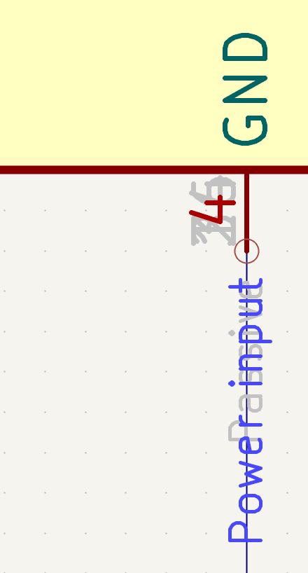
Exploded pin stack (separate pins)
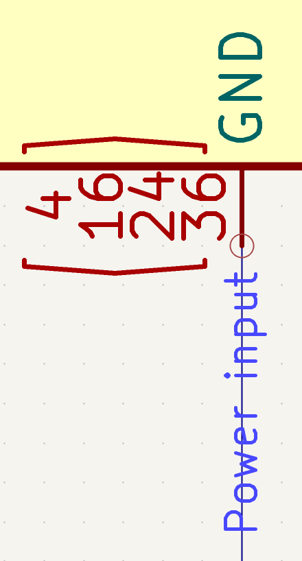
Single pin with multiple pin numbers
You can convert an exploded pin stack (a stack of individual pins) to a single pin with multiple pin numbers by right clicking the pin stack and choosing Convert Stacked Pins. You can do the reverse operation, converting a single pin with multiple pin numbers to a stack of individual pins, by right clicking the pin and choosing Explode Stacked Pin.
When working with exploded pin stacks (a stack of separate pins), there are several considerations to keep in mind.
-
Typically, the top pin in the stack is visible, but the other pins in the stack should be marked as invisible. This has the advantage of avoiding the crowded appearance of multiple pins, their numbers, and their names printed on top of each other, but the disadvantage of not clearly showing that the additional pins exist.
-
The top pin can be set to the most appropriate electrical type, but the other pins should usually be set to the Passive electrical type. This allows ERC to check connections to the pin stack, while avoiding ERC conflicts between pins in the stack. If the pin type is Power Input, it’s especially important to set the hidden pins to Passive because this avoids creating hidden power input pins, which act as global labels.
| Invisible pins with the Power Input type act like global labels. |
Defining pins for multiple units and body styles
Symbols with multiple units and/or graphical representations are particularly problematic when creating and editing pins. Most commonly, pins are specific to each symbol unit (because each unit has a different set of pins) and to each body style (because the form and position is different between the normal body style and the alternate form).
The symbol library editor allows the simultaneous creation of pins. By default, changes made to a pin are made for all units of a multiple unit symbol and to both representations for symbols with an alternate symbolic representation. The only exception to this is the pin’s graphical type and name, which remain unlinked between symbol units and body styles. This dependency was established to allow for easier pin creation and editing in most cases. This dependency can be disabled by toggling the ![]() icon on the main tool bar. This will allow you to create pins for each unit and representation completely independently.
icon on the main tool bar. This will allow you to create pins for each unit and representation completely independently.
Pins can be common or specific to different units. Pins can also be common to both symbolic representations or specific to each symbolic representation. When a pin is common to all units, it only has to drawn once. Pins are set as common or specific in the pin properties dialog.
An example is the output pin in the 7400 quad dual input NAND gate. Since there are four units and two symbolic representations, there are eight separate output pins defined in the symbol definition. When creating a new 7400 symbol, unit A of the normal symbolic representation will be shown in the library editor. To edit the pin style in the alternate symbolic representation, it must first be enabled by selecting the alternate representation with the dropdown control. To edit the pin number for each unit, select the appropriate unit using the drop down control.
Alternate pin function definitions
Symbol pins can have alternate pin functions defined for them. Alternate pin functions allow you to select a different name, electrical type, and graphical style for a pin when a symbol has been placed in the schematic. This can be used for pins that have multiple functions, such as microcontroller pins.
Alternate pin functions are added in the Pin Properties dialog as shown below. Each alternate definition contains a pin name, electrical type, and graphic style. This microcontroller pin has all of its peripheral functions defined in the symbol as alternate pin names.
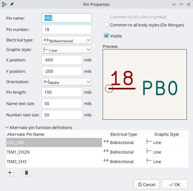
Alternate pin functions are selected in the Schematic Editor once the symbol has been placed in the schematic. For information on using alternate pin functions in the schematic, see the schematic editor symbol documentation.
Pushing pin properties to other pins
You can apply the length, name size, or number size of a pin to the other pins in the symbol by right clicking the pin and selecting Push Pin Length, Push Pin Name Size, or Push Pin Number Size, respectively. All other pins in the symbol will be updated.
Pin table
Another way to edit pins is to use the Pin Table, which is accessible via the ![]() button. The Pin Table displays all of the pins in the symbol and their properties in a table view, so it is useful for making bulk pin changes.
button. The Pin Table displays all of the pins in the symbol and their properties in a table view, so it is useful for making bulk pin changes.
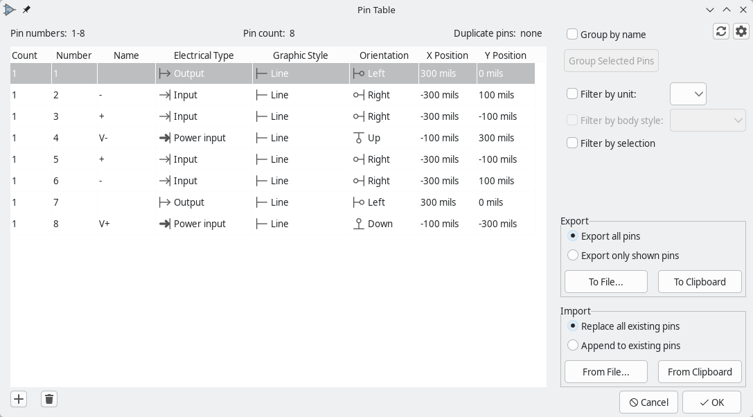
Any pin property can be edited by clicking on the appropriate cell. Pins can be added and removed with the ![]() and
and ![]() icons, respectively.
icons, respectively.
| Columns of the pin table can be shown or hidden by right-clicking on the header row and checking or unchecking additional columns. Some columns are hidden by default. |
You can edit the same property for multiple pins simultaneously by grouping pins. Pins can be automatically grouped by name with the Group by name checkbox, or you manually group several pins by selecting them and clicking Group Selected Pins. Click the ![]() button to clear the manual grouping. You can also filter the table to only display pins in certain units or body styles, or filter to the pins selected in the symbol editor.
button to clear the manual grouping. You can also filter the table to only display pins in certain units or body styles, or filter to the pins selected in the symbol editor.
If Highlight on cross-probe is enabled in the ![]() menu, pins will be highlighted in the symbol editor when you select them in the pin table.
menu, pins will be highlighted in the symbol editor when you select them in the pin table.
You can also import and export pins from the pin table. This lets you define and edit pins in an external spreadsheet tool. Especially for symbols with many pins, this may be more convenient than editing them within KiCad.
To export pins from the table, click either the To File… or To Clipboard button. The pins are exported in a comma-separated (CSV) format. All columns are exported, even if they are hidden in the table. If Export all pins is selected, all pins in the symbol are included. If Export only shown pins is selected, only the pins shown in the table are included.
To import pins into the table, click either the From File… or From Clipboard button. Data for import needs to be in either comma-separated (CSV) or tab-separated (TSV) format. A header row with column names is required: columns in the imported data are mapped to columns in the pin table by name. Any columns in the imported data that don’t match a column in the pin table will be skipped, and any columns that are missing in the imported data will be filled with default values in the pin table. If Replace all existing pins is selected, the pins in the table are completely replaced by the imported pins. If Append to existing pins is selected, the imported pins are added to the table without modifying or replacing the existing pins.
Symbol fields
Symbols contain multiple fields, which are named values containing information related to the symbol. Fields can be displayed on the schematic or hidden and only shown in the symbol’s properties. Some fields have special meaning to KiCad: Reference and Footprint are both critical for creating a PCB, for example. Other fields may contain information that is important for a design but is not interpreted by KiCad, like pricing or stock information for a part.
Any fields defined in a library symbol will be included in the symbol when it is added to a schematic. You can also add new fields to symbols in the schematic. Whether they are in the library symbol or not, these fields can then be edited on a per-symbol basis in the schematic. They are also transferred to the symbol’s corresponding footprint in the PCB.
| Symbol fields are different than graphic text. In addition to being named, fields can be moved and edited in the schematic, while symbol text can only be edited in the symbol editor. |
All library symbols are defined with five default fields: Reference, Value, Footprint, Datasheet, and Description, which are added whenever a symbol is created. These default fields cannot be deleted. Only the Reference field is required to have a value: the contents of a library symbol’s Reference field is used as the reference designator prefix when the symbol is added to a schematic. In the schematic, the symbol’s Reference field contains the entire reference designator.
The Footprint field, if used, contains a reference to a footprint for the symbol. The format is LIBNAME:FOOTPRINTNAME, where LIBNAME is the name of the footprint library in the footprint library table (see the Footprint Library Table section in the PCB Editor manual) and FOOTPRINTNAME is the name of the footprint in the library LIBNAME.
The Description field can contain text describing the symbol such as the component function, distinguishing features, and package options. Together with the symbol’s name and keywords, text in this field is used when searching for symbols in the Symbol Chooser or Symbol Editor. Before KiCad version 8.0, this was a dedicated property (like the symbol name and keywords) rather than a symbol field.
Symbols defined in libraries are typically defined with only these five default fields. Additional fields such as vendor, part number, unit cost, etc. can be added to library symbols but generally this is done in the schematic editor so the additional fields can be added to every symbol in the schematic, not just all symbols of one type.
| A convenient way to create additional empty symbol fields is to use define field name templates. Field name templates define empty fields that are added to each symbol when it is inserted into the schematic. Field name templates can be defined globally (for all schematics) in the Schematic Editor Preferences, or they can be defined locally (specific to each project) in the Schematic Setup dialog. |
| If you want to manage a large amount of component data in symbol fields, consider using database libraries. |
To edit an existing symbol field, double-click the field, select it or hover and press E, or right-click on the field text and select Properties….
To add new fields, delete optional fields, or edit existing fields, use the ![]() icon on the main tool bar to open the Symbol Properties dialog. Fields can be arbitrarily named, but names starting with
icon on the main tool bar to open the Symbol Properties dialog. Fields can be arbitrarily named, but names starting with ki_, e.g. ki_description, are reserved by KiCad and should not be used for user fields.
Fields have a number of properties, each of which is shown as a column in the properties grid. Not all columns are shown by default; columns can be shown or hidden by right clicking on the grid header and selecting or deselecting columns from the menu.
| You can edit fields for many symbols at once using the Symbol Fields Table, which lets you edit the fields of all symbols in the same library at once. |
Footprint filters
The footprint filters tab is used to define which footprints are appropriate to use with the symbol. The filters can be applied in the Footprint Assignment tool so that only appropriate footprints are displayed for each symbol.
Multiple footprint filters can be defined. Footprints that match any of the filters will be displayed; if no filters are defined, then all footprints will be displayed.
Filters can use wildcards: * matches any number of characters, including zero, and ? matches zero or one characters. For example, SOIC-* would match the SOIC-8_3.9x4.9mm_P1.27mm footprint as well as any other footprint beginning with SOIC-. The filter SOT?23 matches SOT23 as well as SOT-23.
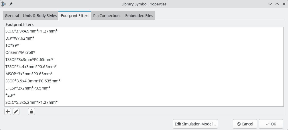
Jumper pins
You can configure a symbol to jumper some or all of its pins internally. Any jumpered pins will always have the same net; they are considered shorted together, even if they are not explicitly connected together in the schematic and PCB.
Symbols with jumper pins represent components that internally short together multiple pins. Examples of such components are wire jumpers, connectors with multiple connected shield pins, and switches with multiple shorted pins on each side of the switch.
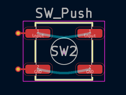
A footprint without jumpered pads. The ratsnest shows missing connections between same-numbered pads.
The same footprint in the same circuit with same-number pads jumpered (internally connected by the component). PCB connections between the same-numbered pads are no longer required.
Because KiCad considers the jumpered pins to be shorted by the component, you only need to connect to one of the shorted pins in the schematic and PCB.
| Jumper pins are different than net ties. A net tie allows copper to bridge two different nets, and each pad in the net tie has a different net. With jumper pins, each pin has the same net, and the electrical connection between jumper pins is assumed to be off-board in the attached component. |
You can configure jumper pins in the Pin Connections tab of a symbol’s Properties.
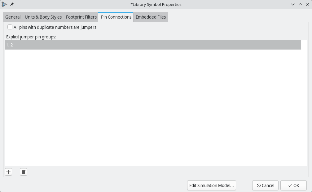
When the All pins with duplicate numbers are jumpers setting is enabled, all pins (and pads in the linked footprint) will be jumpered to the other pins with the same number. For example, all pins numbered 1 will be considered connected to each other.
You can also configure jumper pin groups for pins that don’t have the same number by adding Explicit pin jumper groups with the ![]() button. Enter multiple pin numbers separated by spaces or commas. A pin jumper group with the text
button. Enter multiple pin numbers separated by spaces or commas. A pin jumper group with the text 1 2 or 1, 2 will jumper together pins 1 and 2. A group with 3 4 5 or 3, 4, 5 will jumper together pins 3, 4, and 5.
| Like many other symbol properties, a symbol’s jumper pin settings are transferred to the linked footprint. You can also configure a footprint’s jumper pads using the Footprint Editor. |
Embedding files
External files can be embedded within a symbol. Embedding a file stores a copy of the file inside the symbol. The symbol can then refer to the embedded copy of the file instead of the external file, which makes the symbol more portable as it doesn’t rely on an external file, although the symbol library’s filesize is increased as a result. In symbols this is especially useful for embedding datasheets and SPICE models.
In the symbol editor, you can embed files into library symbols in the Embedded Files tab of a symbol’s properies.
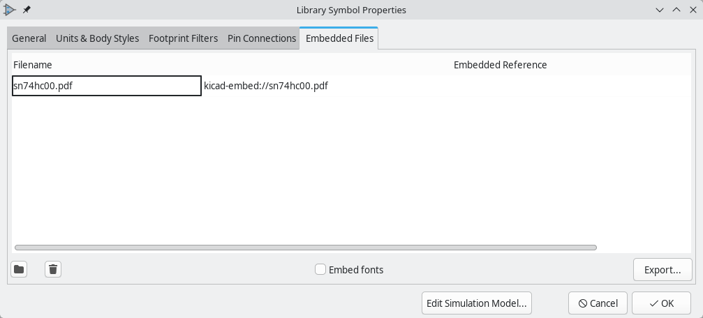
| You can add a datasheet, or a SPICE model, to a symbol and embed it in one step. To do so, browse for a datasheet (in the Symbol Properties dialog) or a SPICE model (in the SPICE Model Editor) and enable the Embed File checkbox in the file browser while choosing a file. This embeds the file and automatically uses the embedded reference as the file path instead of the path to the external file. |
Files embedded in a symbol are deduplicated when the symbol is added to a schematic: if a file is embedded in a symbol, and multiple instances of that symbol are added to the schematic, only one copy of the file will be embedded, and all of the schematic instances will refer to the same embedded file.
When a symbol is derived from a symbol with embedded files, the derived symbol can access both its own embedded files and the files embedded in the parent symbol. Files embedded in a symbol cannot be referred to in the parent schematic outside of the symbol.
File embedding is explained in more detail in the Schematic Setup documentation.
Creating power symbols
Power symbols are symbols that are used to label a wire as part of a global power net, like VCC or GND. The power symbol’s Value field determines the net label. The behavior of power symbols is described in the electrical connections section. Power symbols are handled and created the same way as normal symbols, but there are several additional considerations described below.
It may be useful to place power symbols in a dedicated library. KiCad’s symbol library places power symbols in the power library, and users may create libraries to store their own power symbols. If the Define as power symbol box is checked in a symbol’s properties, that symbol will appear in the Schematic Editor’s Add Power Symbol dialog for convenient access.
Power symbols consist of a single pin of type Power Input. They must also have the Define as power symbol property checked.
In previous versions of KiCad, a power symbol’s pin needed to be both a
power input pin and invisible, and the pin’s name determined the name of
the net that the power symbol connected with. Beginning in KiCad version
8, the pin in a power symbol does not need to be invisible, and the net is
determined by the power symbol’s Value field.
|
Below is an example of a GND power symbol.
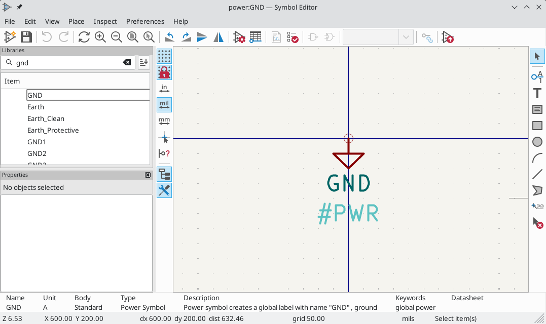
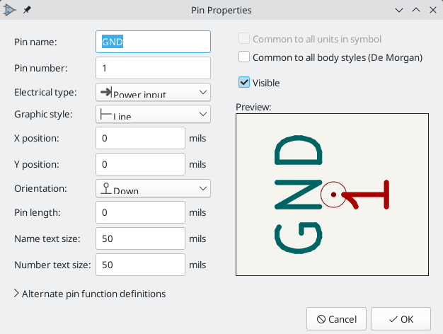
Para crear un símbolo de potencia siga los siguientes pasos:
-
Add a pin of type Power input. Make the pin number
1, the length0, set the graphic style to Line, and make the pin visible. The pin number, name, length, and line style do not matter electrically. -
Place the pin on the symbol anchor. This is not required but makes it easier to place the power symbol in the schematic.
-
Use the shape tools to draw the symbol graphics.
-
Set the symbol value to the desired net name. The symbol value is electrically important: it determines the symbol’s connected net name. This field can be changed later, after the symbol has been placed in the schematic, which will change which net the symbol connects to.
-
Check the Define as power symbol box in Symbol Properties window. This makes the symbol appear in the Add Power Symbol dialog, prevents the symbol from being assigned a footprint, and excludes the symbol from the board, BOM, and netlists.
-
Also deselect the Show pin number and Show pin name options in the Symbol Properties window. This is not necessary but improves the symbol’s appearance.
-
Set the symbol reference and uncheck the Show box. The reference text is not important except for the first character, which should be
#. For the power symbol shown above, the reference could be#GND. Symbols with references that begin with#are not added to the PCB, are not included in Bill of Materials exports or netlists, and they cannot be assigned a footprint in the footprint assignment tool. If a power symbol’s reference does not begin with#, the character will be inserted automatically when the annotation or footprint assignment tools are run.
An easier method to create a new power symbol is to use another symbol as a starting point.
Creating derived symbols
Symbols can be derived from another symbol in the same library. Derived symbols share the base symbol’s graphical shape and pin definitions, but can override the base symbol’s metadata (value, footprint, datasheet, other fields, description, footprint filters, etc.). Any user-defined fields from the base symbol that are not overridden by the derived symbol are directly inherited.
Derived symbols can be used to define symbols that are similar to a base part. For example, 74LS00, 74HC00, and 7437 symbols could all be derived from a 7400 symbol, because they are all quad NAND gates with the same pinout.
| In previous versions of KiCad, derived symbols were referred to as aliases. |
To create a derived symbol, click the ![]() button. This will create a new symbol in the active symbol library.
button. This will create a new symbol in the active symbol library.
| The derived symbol must be created in the same library as the base symbol. |
Choose a name for the symbol in the Symbol name field, and choose a base symbol from the Derive from existing symbol dropdown.
| As a shortcut for choosing a base symbol for a new derived symbol, you can right click an existing symbol in the library tree and choose Derive from existing symbol…. This opens the New Symbol dialog and preselects the existing symbol as the base symbol. |
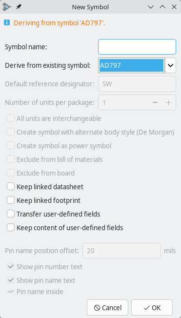
When you are creating a derived symbol, most options in this dialog are disabled because the settings are taken from the base symbol. Several options are only applicable to derived symbols, however:
-
Keep linked datasheet: if enabled, the value of the
Datasheetfield from the base symbol is also used in the derived symbol. If not enabled, theDatasheetfield is empty in the derived symbol. -
Keep linked footprint: if enabled, the value of the
Footprintfield from the base symbol is also used in the derived symbol. If not enabled, theFootprintfield is empty in the derived symbol. -
Transfer user-defined fields: if enabled, each user-defined field in the base symbol will also be created as an empty field in the derived symbol. If this option is not selected, the derived symbol automatically inherits the fields and their values from the base symbol.
-
Keep content of user-defined fields: if enabled, the value of each user-defined field in the base symbol will also be set in the derived symbol.
When you click OK, a new derived symbol will be created in the active library.
The derived symbol has the same graphics and pins as the base symbol; therefore, its graphics and pins are not editable. You can only edit the graphics and pins of a derived symbol by editing its base symbol; this will affect the base symbol and any other symbols that are derived from it.
Derived symbols inherit all user-defined fields from the base symbol. This means that derived symbols automatically have all the user-defined fields (and their values) from the base symbol. Inherited fields are displayed in italics to show that they are inherited from the base symbol. You can override an inherited field by giving the field a different value in the derived symbol.
Derived symbols are required to be in the same symbol library as their base symbol. If you perform a Save As on a derived symbol to move it into a new library, the base symbol will also be saved in the new library. To save a derived symbol into a new library without its base symbol, you can flatten the derived symbol.
Flattening derived symbols
You can convert an existing derived symbol into a fully-defined base symbol by right clicking the derived symbol in the library tree and choosing Flatten Symbol. This breaks the derived relationship between the derived symbol and its base symbol. After flattening, all of the graphics, pin definitions, fields, and other metadata are fully defined in the formerly-derived symbol, but are otherwise identical to what they were before the symbol was flattened.
| Derived symbols must be in the same library as their base symbol. Flattening a derived symbol allows the formerly-derived symbol to be moved to a different library. |
You can also flatten derived symbols while performing a Save As operation. Ordinarily, performing a Save As on a derived symbol maintains the existing derived relationship between the derived symbol and its base symbol: the newly saved symbol is still derived from the original base symbol. But if the Flatten/remove symbol inheritance option is checked in the Save As dialog, the derived symbol will be saved as a base symbol.
Bulk editing symbol fields
The Symbol Fields Table allows you to view and modify field values for all symbols in a library using a spreadsheet interface. This is similar to the Symbol Fields Table in the Schematic Editor, but it contains the fields for all symbols in a given library rather than all symbols in a schematic.
You can open the Symbol Fields Table by right clicking on a symbol in the Library Tree panel and choosing Bulk Edit Symbol Fields…. This opens the Symbol Fields Table to edit the fields of all symbols in the same library.
If the symbol is derived or has other symbols that derive from it, you can alternatively choose Bulk Edit Related Symbol Fields…. This also opens the Symbol Fields Table, but shows the fields for the base symbol and all symbols that derive from it.
When the dialog is open, you can switch between editing the whole library’s symbols and just related symbols using the dropdown menu at the top of the window.
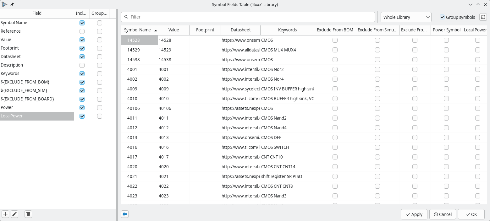
The main table has a row for each symbol and a column for each field. Each cell is editable. Symbol attributes (Exclude From BOM, Exclude From Simulation, Exclude From Board, Power, and Local Power) are shown as checkboxes.
The left pane contains a list of all available symbol fields and attributes. You can add or remove any symbol field from the main table on using the Include checkboxes (fields can also be shown or hidden by right-clicking on the header of the main table). New symbol fields can be added using the ![]() button; a field with that name will be added to every symbol. To rename the field, which changes the field name in all symbols, use the
button; a field with that name will be added to every symbol. To rename the field, which changes the field name in all symbols, use the ![]() button. The
button. The ![]() button deletes the field from all symbols. You can collapse this panel by clicking the
button deletes the field from all symbols. You can collapse this panel by clicking the ![]() button.
button.
Similar symbols can optionally be grouped by any symbol field using the Group By checkboxes. Symbols are grouped into a single row in the table if all of their Group By fields are identical. The grouped row can be expanded to show the individual symbols by clicking the arrow at the left of the row. The Group symbols checkbox enables or disables symbol grouping, and the ![]() button recalculates groupings.
button recalculates groupings.
Symbols can be filtered by symbol name using the Filter textbox at the top. The filter supports wildcards: * matches any number of any characters, including none, and ? matches any single character.
Checking symbols
The Symbol Editor can check for common issues in your symbols. Run the symbol checker using the ![]() button in the top toolbar.
button in the top toolbar.
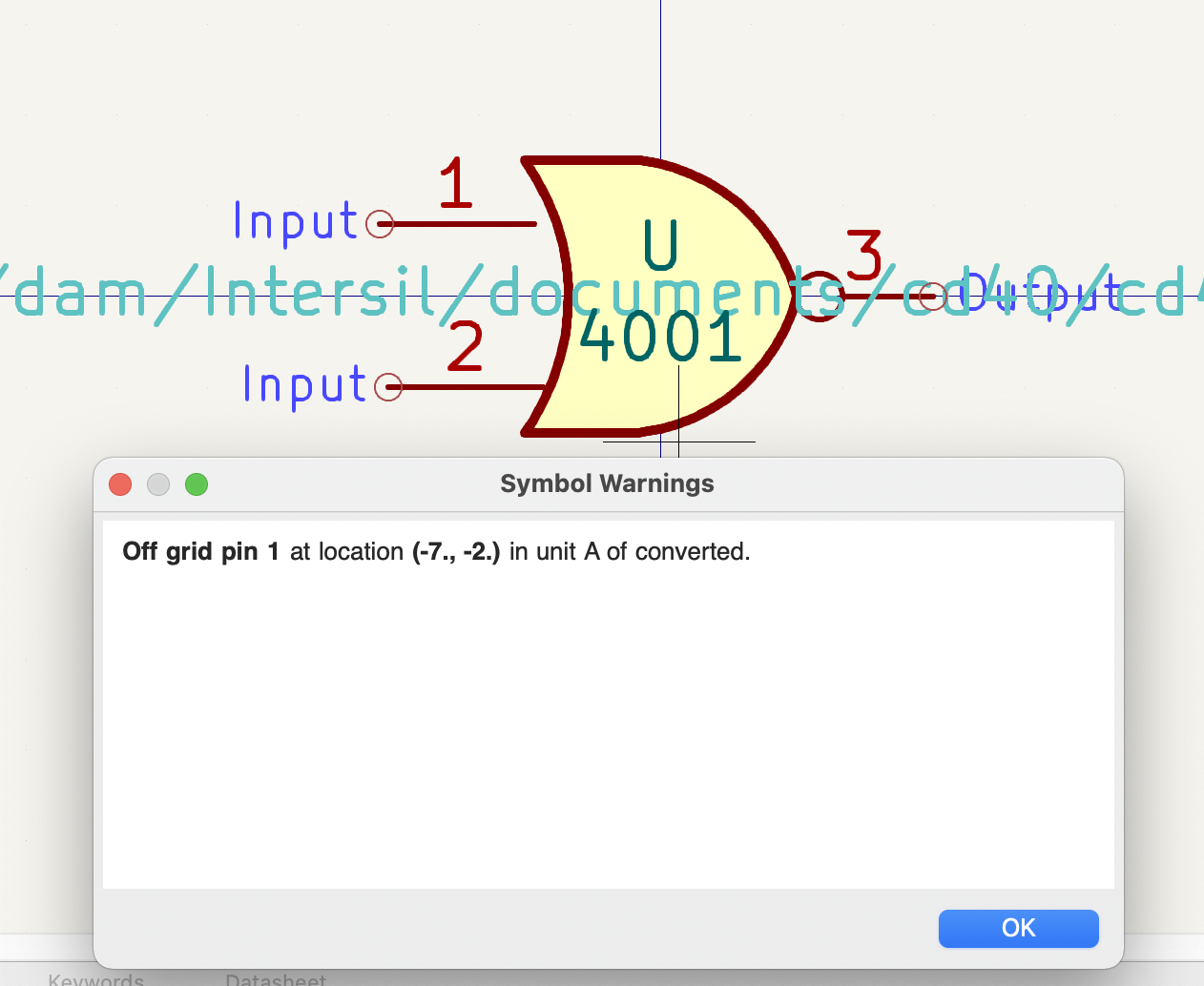
The symbol checker checks for:
-
Pins that are off-grid (pins are considered off grid if their position is not a multiple of the current symbol editor grid. It is strongly recommended to use a 50 mil grid for symbol pins)
-
Pins that are duplicated
-
Issues with graphical shapes, such as zero-sized shapes
-
Illegal reference designator prefixes: reference designator prefixes should not end with a number or
? -
Incorrectly designed power symbols. Power symbols should have:
-
A single unit
-
No alternate body styles
-
A single pin which is either of type Power Output (see PWR_FLAG) or visible and of type Power Input (see power symbols)
-
-
Hidden Power Input pins in non-power symbols: these create implicit connections and are not recommended
| In previous versions of KiCad, power symbols required an invisible power input pin so that they would make a global connection. In KiCad 8, the power input pin does not need to be invisible. Therefore the symbol checker will report if invisible power input pins are detected. |
Importing symbols
You can import symbols from an external KiCad library into one of your symbol libraries using File → Import → Symbol…. The source library does not have to be part of your library configuration, but the destination must be a loaded library.
| If you a KiCad symbol from the internet, importing it is a good way to add it to your libraries. |
When you start the symbol importer, you are first asked to browse to a library that contains the symbol(s) you want to import. The destination library is the library that is active in the Symbol Editor.
Once you select a source library, all of the symbols in that library are listed. Clicking a symbol in the list shows it in the preview canvas. Any symbols that are selected using the checkboxes next to their names are imported when you click the Import button.
Derived symbols are indicated with a circle in front of their names. Derived symbols cannot be imported by themselves; when you import a derived symbol, the base symbol is automatically imported as well.
| If the source library is already part of your library configuration, an easier way to transfer a symbol from one library to another is to use File → Save As… (or Save Copy As…). |
Importing schematics from other applications
KiCad can import complete schematics saved in several third-party EDA tool formats, converting them to KiCad’s native format in a single step. This allows you to migrate existing designs without having to recreate them from scratch.
Importing a schematic replaces the current schematic with the contents of the imported
file. It does not merge the foreign schematic into an existing KiCad design. After
import, save the schematic using File → Save to create a KiCad .kicad_sch file.
|
How to import a schematic
To import a schematic from a supported third-party format, use File → Import → Non-KiCad Schematic….
An "Import Schematic" file dialog will open. The dialog presents an "All supported formats" filter that includes all importable file types, as well as individual format filters. Select the desired source file and click Open.
KiCad reads the foreign file, converts it to KiCad format, and loads the result into the schematic editor. If the importer encounters any issues during conversion, a report dialog will appear listing warnings and unsupported features.
| If you open a file using File → Open… and the file is not a KiCad schematic, the Schematic Editor will display a message directing you to use File → Import → Non-KiCad Schematic… instead. |
Supported formats
KiCad supports importing schematics from the following EDA tools:
| Source EDA Tool | File Extension(s) | Notes |
|---|---|---|
Altium Designer |
|
Multi-sheet designs are supported; each |
Eagle (Autodesk) |
|
Eagle version 6.x and later (XML format). |
LTspice |
|
LTspice schematic and simulation files. |
PADS Logic |
|
PADS Logic ASCII export format. |
CADSTAR Schematic Archive |
|
Zuken CADSTAR schematic archive files. |
gEDA / Lepton EDA |
|
gEDA gschem and Lepton EDA schematic files. |
EasyEDA (JLCEDA) Standard |
|
EasyEDA Standard edition JSON export. |
EasyEDA (JLCEDA) Professional |
|
EasyEDA Professional edition project files. |
The Eagle .sch extension and the gEDA .sch extension are both used by their
respective tools. KiCad identifies the correct format automatically based on the
file contents.
|
The PADS Logic .asc extension is shared with LTspice. KiCad inspects the file
header to determine which format applies.
|
Format-specific notes
Altium Designer
KiCad imports Altium Designer schematic files (.SchDoc). Altium projects can contain multiple sheets, each saved as a separate .SchDoc file. When you import one sheet, KiCad will also attempt to load the other sheets referenced by that project, reconstructing the sheet hierarchy.
Symbols found in the source file are placed into a generated symbol library that is saved alongside the imported schematic.
If you have a complete Altium project (.PrjPcb) with both schematic and PCB files,
the KiCad Project Manager can import both in a single step. Use File →
Import Non-KiCad Project… → Altium Project… and select the .PrjPcb
file. The .SchDoc import described here is for schematic files imported on their
own.
|
Eagle (Autodesk)
KiCad imports Eagle XML schematic files (.sch), which are the format produced by Eagle version 6.x and later. Eagle schematics store all sheets in a single file.
Symbols are extracted from the embedded Eagle libraries and placed into a generated KiCad symbol library.
| Binary Eagle files created by versions earlier than 6.x are not supported. Open the file in Eagle first and re-save it to convert to the XML format before importing. |
LTspice
KiCad imports LTspice schematic files (.asc). These are the simulation schematics created by LTspice, which uses its own symbol library and netlist conventions.
After import, the schematic will reflect the circuit topology from LTspice, but simulation directives and LTspice-specific elements such as SPICE parameters and behavioral sources may not convert fully. Review the imported schematic and the KiCad SPICE simulator documentation before attempting to run simulations on an imported LTspice design.
PADS Logic
KiCad imports PADS Logic schematic files (.asc or .txt). These are the ASCII text exports produced by the PADS Logic schematic editor. To generate this file from PADS Logic, use File → Export and select the ASCII format.
CADSTAR Schematic Archive
KiCad imports CADSTAR Schematic Archive files (.csa) from Zuken’s CADSTAR tool.
In addition to full schematic import, KiCad can use CADSTAR Parts Library files (.lib) as read-only symbol libraries through the Symbol Library Manager.
gEDA / Lepton EDA
KiCad imports gEDA gschem and Lepton EDA schematic files (.sch). These are ASCII text files produced by the gEDA suite or its fork, Lepton EDA.
Symbols in gEDA schematics reference external .sym files from the gEDA system symbol library. KiCad will search standard gEDA library locations for these symbol files during import. Symbols that cannot be found are replaced with a fallback rectangular symbol. Hierarchical sheets are supported; KiCad will recursively import sub-schematics referenced by source= attributes on component instances.
EasyEDA (JLCEDA) Standard
KiCad imports EasyEDA Standard edition schematic files (.json). To obtain a file for import, export your design from EasyEDA using the Export EasyEDA option, which produces a JSON file.
Symbols are extracted from the embedded library data within the JSON file and placed into a generated KiCad symbol library.
EasyEDA (JLCEDA) Professional
KiCad imports EasyEDA Professional edition project files (.epro or .zip).
For projects containing multiple schematics, KiCad will present a project chooser dialog so you can select which schematic within the project to import.
After importing
After importing a schematic from a third-party tool, review the result and perform any necessary cleanup:
-
Save the schematic: Use File → Save to save the imported design as a KiCad
.kicad_schfile. The file will be placed in the current project directory with the project name. -
Run the Electrical Rules Check (ERC): Select Inspect → Electrical Rules Checker to identify any connectivity or symbol issues introduced during import.
-
Review the import report: If the importer produced warnings, the report dialog will have been shown automatically. Review any warnings about unsupported features or items that could not be converted.
-
Remap symbols: Imported symbols are stored in a generated library created alongside the schematic. If you want to use KiCad standard library symbols instead, use Tools → Edit Symbol Fields to reassign symbols to your preferred library. The symbol remapping tool may also be useful.
-
Assign footprints: Third-party schematics rarely use KiCad footprint references. Use Tools → Assign Footprints to link each symbol to an appropriate KiCad footprint before proceeding to board layout.
-
Check the drawing sheet: Imported schematics do not carry a KiCad drawing sheet (title block). The schematic editor will use an empty drawing sheet after import. To add a title block, open File → Page Settings and choose a drawing sheet template.
Design blocks
Design blocks are a design-reuse feature that lets you save a portion of a schematic (and optionally a corresponding PCB layout) as a named, reusable fragment stored in a design block library. You can instantiate a design block any number of times within the same project or across different projects. Design blocks are organized in libraries in the same way that symbols and footprints are organized in their respective libraries.
A single design block can contain a schematic fragment, a PCB layout fragment, or both. When you place a schematic design block, the saved schematic fragment is inserted into the current schematic sheet or into a new hierarchical subsheet. If the design block also contains a layout fragment, you can later apply that layout to the footprints that were placed as a result of the schematic fragment. This makes design blocks well suited for circuits that appear repeatedly across projects, such as power supply subcircuits, filter networks, protection circuits, and interface conditioning stages.
Typically, design blocks are created first as a schematic fragment, with the layout added later once the circuit has been placed and routed on a board. Reusing layout fragments in design blocks is covered in the PCB Editor manual.
Design block concepts
Two ways to place a design block
When you place a design block into a schematic you choose between two fundamentally different placement modes:
Place inline (no sheet): The contents of the design block are inserted directly into the current schematic sheet alongside all other schematic objects. The content becomes part of the current sheet and can be edited in place.
Place as sheet: The contents of the design block are placed into a new hierarchical subsheet. The current schematic sheet receives a hierarchical sheet symbol whose contents are the design block’s schematic. Placing as a sheet is useful when the design block represents a logically distinct functional block, when you want the design block contents to be visually separate from the parent schematic, or when you plan to reuse the same sheet multiple times as a repeated hierarchical sheet. Default fields defined in the design block’s properties are applied as hierarchical sheet fields when placing as a sheet.
In either mode, also enable the Place as group option to wrap the placed content in a group with a library link. Without a group, features including saving changes back to the library, placing additional linked instances, and applying the stored layout to the corresponding footprints in the PCB editor are not available. The Place as group option works with both placement modes: when enabled alongside Place as sheet, a group wrapping the sheet symbol is added to the parent schematic.
| Design blocks do not support nested hierarchical sheets. If the sheet you are saving as a design block contains hierarchical sheet symbols (subsheets), the save operation will be rejected. |
The library link
When a design block is placed as a group, the group stores a library link in the format <library>:<block> — for example, analog_filters:sallen_key_lowpass. This link connects the placed instance to its source in the library and enables the following operations:
-
Save to Linked Design Block — push edits made to the placed group back to the library, updating the stored design block schematic.
-
Place Linked Design Block — place another instance of the same design block as a new linked group, without reopening the Design Blocks panel.
-
Apply Design Block Layout — in the PCB editor, apply the layout stored in the linked design block to the group of footprints corresponding to this design block instance. As an alternative, the multichannel tool can replicate a manually completed layout from one group to another without requiring a stored layout fragment in the design block.
A group that does not have a library link cannot use any of these operations. If you manually grouped the contents of a design block without using the Design Blocks panel, you can add the library link retroactively in the group’s properties dialog (see Setting a library link manually).
Setting a library link manually
If you have a group in your schematic that contains the same content as an existing design block but the group does not have a library link, you can add the link without re-placing the design block:
-
Select the group and open its properties (right click → Group Properties…, or press E with the group selected).
-
In the Library link field, enter the design block identifier in the format
<library>:<block>. For example,power_circuits:ldo_3v3. -
Click OK.
The group will now behave as a linked group and all library-linked operations will be available.
If you want the design block’s schematic contents to also be grouped in the PCB, either for organizational purposes or so you can apply a design block layout, use the Update PCB from Schematic tool with the Group footprints based on symbol groups option enabled.
Design block library structure
Design block libraries are stored as directories on the filesystem. The directory structure has two levels of nesting:
-
The library itself is a directory whose name ends with
.kicad_blocks(for example,my_power_circuits.kicad_blocks). -
Each design block within the library is a subdirectory inside the library directory, with the suffix
.kicad_block(for example,ldo_3v3.kicad_block). -
Inside each design block directory, KiCad stores:
-
A schematic file (
<block_name>.kicad_sch) — present if the design block contains a schematic fragment. -
A board file (
<block_name>.kicad_pcb) — present if the design block contains a layout fragment. -
A metadata file (
<block_name>.json) — always present; stores the design block’s description, keywords, and default fields.
-
Because libraries and design blocks are plain filesystem directories, they can be managed with ordinary file manager tools, version control systems, or shared over a network filesystem. The library tables (see below) must be updated if library directories are moved or renamed outside of KiCad.
Global and project library tables
As with symbol and footprint libraries, design block libraries are registered in library tables before KiCad can use them. There are two library tables:
-
The global design block library table lists libraries that are available in every KiCad project. The global table is shared across all projects on the same machine.
-
The project design block library table lists libraries that are available only in the current project. The project table is stored alongside the project files.
Both tables are managed through Preferences → Manage Design Block Libraries…. The dialog behaves identically to the symbol and footprint library table dialogs. See the symbol library table documentation for a full description of the library table interface.
The Design Blocks panel
To use schematic design blocks, first show the Design Blocks panel by clicking View → Panels → Design Blocks. This opens a docked panel on the right side of the schematic editor. To close the panel, use the same menu entry again, click the close button in the top right of the panel, or right click in the panel and choose Hide Library Tree.
The Design Blocks panel lets you create design block libraries and create, edit, and place design blocks in the schematic.
The panel has three main areas:
-
A filter textbox at the top, for searching across all libraries by name, description, and keywords. By default results are ranked by best match. To sort alphabetically instead, select Sort Alphabetically under the
settings menu. -
A library tree that lists all registered design block libraries and the design blocks they contain. Libraries can be expanded or collapsed. A Recently Used pseudo-library at the top of the tree records design blocks you have placed recently. Right click a library and choose Pin Library to keep it at the top of the list regardless of recent usage.
-
A preview area below the tree that shows the name, description, keywords, and a graphical preview of the currently selected design block.
Creating and managing design blocks
Design blocks are saved in design block libraries, so you need to add a library before you can save any design blocks.
Creating a new design block library
To create a new library, right click in the library tree and select New Library…. This opens a file browser for you to choose a location and name for the new library. Design block libraries are saved as a folder; the folder name is the library name plus the suffix .kicad_blocks.
The file browser also lets you choose whether the new library should be added to the global design block library table or the project design block library table. Libraries in the global library table will be available to all projects, while libraries in the project library table will only be available in the current project.
| The global and project design block library tables are managed using Preferences → Manage Design Block Libraries…. This includes deleting and renaming design block libraries. The design block library tables behave in the same way as the symbol and footprint library tables. For more information about managing library tables, see the symbol library table documentation. |
After choosing a name, location, and library table, a new, empty library is created. When you create new design blocks, you can save them in this library.
Creating a new design block
In the schematic editor, design blocks can be created either from the entire contents of a schematic sheet or from a selection of schematic objects. To create and save a new design block, select the desired source objects, either by opening the desired sheet or selecting the objects in the editing canvas. Then right click the design block library that will contain the block and select Save Current Sheet as Design Block… or Save Selection as Design Block… as appropriate.
The two creation commands differ in what they capture:
-
Save Current Sheet as Design Block captures everything on the current schematic sheet. Navigate to the sheet you want to save before invoking this command. This is the most convenient option when the circuit you want to capture already exists on its own dedicated sheet.
-
Save Selection as Design Block captures only the objects that are currently selected in the canvas. Select the symbols, wires, labels, and other schematic objects you want to include before invoking this command. If the selection is a single hierarchical sheet symbol, KiCad saves the contents of that subsheet (equivalent to Save Current Sheet for that sheet). If the selection contains multiple items or a single group, those items are saved as the design block content.
After invoking either command, the Design Block Properties dialog opens.
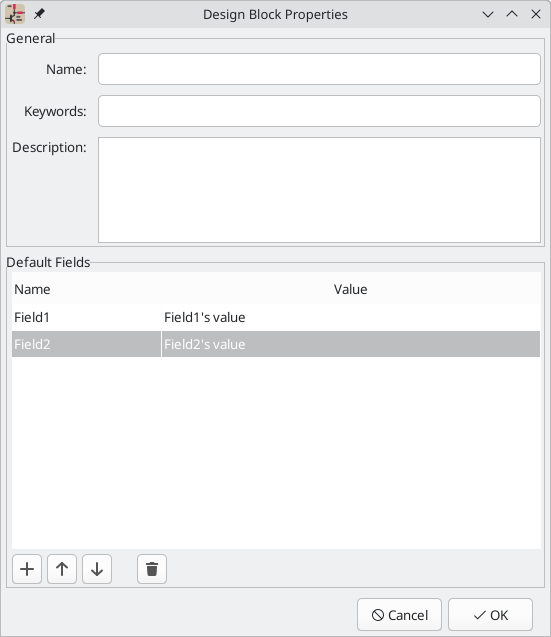
This brings up the Design Block Properties dialog, where you can edit the properties of the new design block.
-
Name: this is the name of the new design block, which is shown in the library tree and the preview pane. It is also used when filtering design blocks with the filter textbox. When design blocks are added as a group or as a schematic sheet, this is the default name of the new group or sheet. The name may not contain the characters
/ : ; \ | < > " * ?or any character that is illegal in a library item name. -
Keywords: these are space-separated keywords describing the design block. They are displayed in the design block preview pane and used when filtering design blocks with the filter textbox.
-
Description: this is a description of the design block, which is shown in the library tree and the preview pane. It is also used when filtering design blocks with the filter textbox.
-
Default Fields: these are key/value pairs which are included as hierarchical sheet fields when the design block’s schematic is placed as a sheet. Fields are ignored when the design block is not placed as a sheet. Use default fields to pre-populate sheet-level parameters such as supply voltage, channel number, or other values that are expected to be overridden when the design block is placed as a sheet.
After filling in the properties and clicking OK, the design block is saved to the selected library. If a design block with the same name already exists in the library, KiCad will ask for confirmation before overwriting it.
When you save a selection as a design block (as opposed to saving an entire sheet), KiCad automatically groups the selected objects and sets the group’s library link to point to the newly created design block. This means the selection is ready for further design block operations immediately after saving.
You can edit a design block’s properties after creating it by right clicking the design block in the design block library tree and selecting Properties….
Deleting a design block
To delete a design block from a library, right click the design block in the library tree and select Delete Design Block. KiCad will ask for confirmation before permanently removing the design block and its directory from the filesystem. This operation cannot be undone.
Deleting a design block from the library does not affect any schematic objects that were previously placed from that design block. Existing placed groups that had a library link to the deleted design block retain their content; they simply lose the ability to use library-linked operations.
Updating an existing design block
There are multiple ways to push schematic changes back to an existing design block in the library. All of them replace the schematic content stored in the design block with new content; they do not merge changes.
Updating from a selection
This is the most general approach and works regardless of how the design block was originally placed:
-
Select the schematic objects that represent the new content for the design block.
-
In the Design Blocks panel, right click the design block you want to update and choose Update Design Block from Selection.
The stored schematic of the design block is replaced by the selection. If the design block previously had a schematic but you are updating with a new one, KiCad will ask for confirmation before overwriting.
Updating from the current sheet
If the current sheet contains exactly the content you want to store in the design block (for example, if the design block was originally placed as a hierarchical sheet and the sheet has since been edited):
-
Navigate to the sheet whose contents you want to store.
-
In the Design Blocks panel, right click the design block you want to update and choose Update Design Block from Current Sheet.
The stored schematic of the design block is replaced by everything on the current sheet.
Saving from a linked group
If the design block was placed as a group and the group has a library link:
-
Edit the schematic contents inside the group.
-
Right click the group in the canvas and choose Save to Linked Design Block.
This is the most direct workflow when iterating on a placed design block instance: edit in place, then push back to the library with a single right click.
| Updating a design block in the library does not automatically update previously placed instances of that design block. Placed instances are independent copies of the design block content at the time they were placed. To bring an existing placed instance in line with the current library version, delete it and place the updated design block again. |
Using design blocks in a schematic
You can place a design block into a schematic using the Design Blocks panel.
The Design Blocks panel contains a library tree that lists your design block libraries and the design blocks contained in each library. Each library can be expanded or collapsed to show or hide the design blocks in that library. There is a Recently Used pseudo-library at the top of the tree that contains any design blocks that you have recently placed. You can pin any libraries to the top of the list by right clicking the library and selecting Pin Library.
You can filter design blocks by their name, description, and keywords using the filter textbox at the top of the Design Blocks panel. By default, matches are sorted by best match, but you can change to sorting alphabetically by selecting Sort Alphabetically under the ![]() menu.
menu.
When you select a design block in the library tree, the design block’s name and metadata are displayed below the library tree along with a graphical preview of the design block. The metadata includes the block’s description and keywords.
To add a design block to the schematic, double click it in the library tree or right click a design block and select Place Design Block.
Placement options
There are several options controlling how the design block is placed:
-
If the Place repeated copies checkbox is enabled, KiCad will begin placing the design block again when you finish placing the previous block. To cancel placing the next block, press Esc or right click and select Cancel.
-
If the Place as group checkbox is enabled, the contents of the design block will be added to a group in the schematic, and the group’s library link will be set to point to the source design block and library. Grouping a design block keeps its contents together as a single unit in the schematic and enables library-linked operations such as saving changes back to the library, placing additional linked instances, and applying the design block layout in the PCB editor. The group can also be copied to the corresponding footprints in the board.
-
If the Place as sheet checkbox is enabled, you will need to click twice in the editing canvas to place two corners of a hierarchical sheet. The design block contents will be placed in the new sheet. If the Place as sheet checkbox is not enabled, clicking once in the canvas will place the contents of the design block directly into the current schematic. Place as group and Place as sheet can be enabled simultaneously: when both are enabled, a new hierarchical sheet is created and a group containing the sheet symbol is added to the parent schematic.
-
If the Keep annotations checkbox is enabled, KiCad will insert the design block without changing the symbol annotations as defined in the saved design block. If it is not enabled, KiCad will reset the symbol annotations while inserting the design block and reannotate all of the symbols in the block according to the current annotation settings. Keeping annotations is useful when you intend to place only a single instance of the design block in the schematic and the original reference designators are meaningful. When placing multiple instances, disable this option so that KiCad assigns unique reference designators to each instance automatically.
After placement
Once placed in a schematic, the contents of a design block behave the same as any other schematic objects and can be edited, moved, deleted, etc. exactly as if they were added to the schematic normally. If the design block was placed as a group, the group boundary is visible in the canvas. You can enter the group to edit individual items inside it, or select the entire group as a unit to move, copy, or delete all of its contents together.
Practical workflows
Workflow: creating a reusable power circuit
This workflow demonstrates saving a power supply subcircuit as a design block and reusing it in multiple projects.
-
Draw the circuit. In the schematic editor, draw the power supply circuit including symbols, wires, net labels, and power symbols. Annotate the schematic and verify it passes ERC.
-
Create or select a library. Open the Design Blocks panel (View → Panels → Design Blocks). If you do not already have a suitable library, right click in the library tree and choose New Library…. Give the library a descriptive name (for example,
power_circuits) and save it to an appropriate location. Add it to the global library table so it is available in all projects. -
Select the circuit. In the canvas, draw a selection box around all the symbols, wires, and labels that make up the power supply circuit.
-
Save as design block. Right click the target library in the Design Blocks panel and choose Save Selection as Design Block…. In the Design Block Properties dialog, enter a meaningful name, a brief description, and relevant keywords (for example,
LDO 3.3V linear regulator). Click OK. KiCad saves the design block and automatically groups the selected objects with a library link to the new design block. -
Reuse in another project. Open a different project. Open the Design Blocks panel and expand the
power_circuitslibrary. Find the design block you created (use the filter if needed). Enable Place as group and, if the reference designators should be reassigned, disable Keep annotations. Double click the design block to begin placement and click in the canvas to place it. -
Update the design block later. If you improve the power supply circuit, select the placed group, edit it as needed, then right click the group and choose Save to Linked Design Block to push the changes back to the library.
Workflow: sheet-based reuse with hierarchical parameters
This workflow is suited for a design block that represents a complete functional block with parameters that vary between instances, such as a per-channel analog conditioning circuit.
-
Draw the circuit on a dedicated sheet. Create a hierarchical sheet in your project and draw the channel circuit on it, using hierarchical labels for signals that connect to the parent sheet. If the circuit has configurable values (such as a gain-setting resistor value), note which sheet fields you will use to communicate these.
-
Define default fields. Open the Design Blocks panel and save the sheet as a design block using Save Current Sheet as Design Block…. In the Design Block Properties dialog, add default fields for each hierarchical parameter. For example, add a field named
GAIN_Rwith a default value of10k. -
Place as a sheet. In the parent schematic, open the Design Blocks panel, select the design block, enable Place as sheet, and click twice in the canvas to define the sheet symbol boundary. KiCad creates a new hierarchical sheet symbol and populates it with the default fields from the design block.
-
Customize each instance. For each placed hierarchical sheet, open the sheet properties and adjust the field values to match the requirements for that particular instance (for example, different resistor values for different gain settings). The sheet contents are shared (all instances use the same underlying schematic file from the design block), but the field values are per-instance.
-
Updating. If the underlying circuit changes, save the modified sheet as an update to the design block using Update Design Block from Current Sheet. All instances of the hierarchical sheet in the project will automatically reflect the updated schematic, because they all reference the same subsheet file.
Simulator
KiCad provides an embedded electrical circuit simulator using ngspice as the simulation engine. ngspice is a SPICE simulator derived from the original widely used Berkeley SPICE program. KiCad’s simulator can also run simulations using IBIS models of device pins.
The process of creating and running a simulation in KiCad has two main parts:
-
Drawing a simulation schematic in KiCad’s Schematic Editor. Schematics for simulations are similar to normal schematics (and can even be identical), but they typically include simulation-specific devices, such as sources, and may exclude devices that are irrelevant for simulation, such as connectors. Creating a schematic simulation requires ensuring all symbols in the schematic have appropriate models assigned. Finding or creating simulation models, and then validating them, can be a significant portion of the process. KiCad includes some simple simulation models for basic devices such as sources, passive devices, and generic semiconductor devices, but beyond those you will need to find or create your own models.
-
Running the simulation using the simulator tool. This includes choosing the type of analysis (transient, AC, etc.) and configuring its options. Multiple different analyses can be performed. The simulator provides a plot window to view and analyze simulation results.
When drawing schematics for simulation, the Simulation_SPICE symbol library, installed with KiCad by default, may be useful. It contains common elements used for simulation such as voltage and current sources, generic semiconductor symbols, and other simulation-specific devices. The symbols in this library are described in detail below.
While these elements enable a great variety of simulation work, users familiar with SPICE in other environments will be used to incorporating models of commercially-available semiconductors, integrated circuits, and other devices as more complex SPICE models. Indeed, semiconductor manufacturers often freely supply these to help users simulate and develop circuits using their parts. Note that while KiCad does not include any commercial SPICE models in its distribution, you are free to use any models you may have, or have used with other circuit simulators, in KiCad’s simulator.
In general, if a model works with other SPICE simulators, it should work with the KiCad simulator, although some SPICE simulators implement extensions that are unsupported by ngspice. ngspice offers several compatibility modes to improve compatibility with other simulators.
Finally, to quickly showcase the capabilities of the KiCad simulator, some demonstration projects are included in the KiCad distribution. They can be found in the demos/simulation directory.
Assigning models
You need to assign simulation models to symbols before you can simulate your circuit.
Each symbol can have only one model assigned, even if the symbol consists of multiple units. For symbols with multiple units, you should assign the model to the first unit.
SPICE model information is stored as text in symbol fields. Therefore you may define it in either the symbol editor or the schematic editor. To assign a simulation model to a symbol, open the Symbol Properties dialog and click the Simulation Model… button, which opens the Simulation Model Editor dialog.
You can exclude a symbol from simulation entirely by checking the exclude from simulation checkbox in the Symbol Properties dialog. Symbols with this attribute set are drawn with a grey outline and a small simulation icon next to them, as shown below.
Inferred models
Resistor, inductor, and capacitor models can be inferred, which means that KiCad will detect that they are passives and automatically assign an appropriate simulation model. Therefore they do not require any special settings; users only need to set the Value field of the symbol.
KiCad infers simulation models for symbols based on the following criteria:
-
The symbol has exactly two pins,
-
The reference designator begins with
R,LorC.
Inferred models are ideal models. If the simulation requires a non-ideal model, for example an inductor with parasitic capacitance included, you must explicitly assign a model that includes it.
Built-in models
KiCad offers several standard simulation models. They do not require an external model file, and their parameters can be edited in KiCad’s Simulation Model Editor GUI. The following devices are available:
-
Resistors (including potentiometers)
-
Capacitors
-
Inductors
-
Transmission lines
-
Switches
-
Voltage and current sources
-
Diodes
-
Transistors (BJTs, MOSFETs, MESFETs, and JFETs)
-
XSPICE code models
-
Raw SPICE elements
To add a built-in model to a symbol, open the Simulation Model Editor dialog (Symbol Properties → Simulation Model…) and select Built-in SPICE model. You can then select the kind of device from the device dropdown and the device subtype from the device type dropdown.
Refer to the ngspice documentation for more details about these models and their parameters.
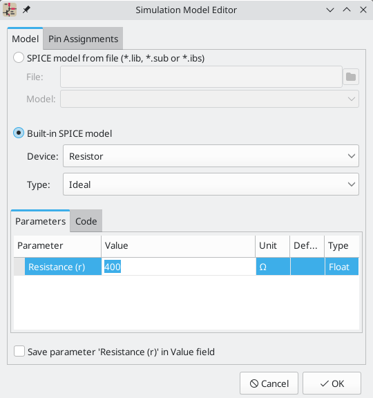
Device sets the type of device to simulate: a resistor, BJT, voltage source,
etc. This value is stored in the symbol’s Sim.Device field.
Device type selects the type of model to use for the device. Most devices
have several types of models to choose from. Models may vary in their degree of
accuracy, which characteristics they are optimized for, what parameters they
have available, and how many pins they have. For example, the ideal
resistor type models a simple resistor with two terminals and a single
resistance parameter, while the potentiometer resistor type models an
adjustable resistor with three terminals and an additional parameter for wiper
position. Some devices have an especially large number of types to choose from:
N-channel MOSFETs, for example, have 17 available types, each of which uses a
different mathematical model to simulate the transistor behavior. One model may
be more or less appropriate than another for simulating a specific device or
circuit or for performing a particular analysis. Refer to the
ngspice documentation for detailed
information about models and their parameters. The device type value is
stored in the symbol’s Sim.Type field.
The parameters tab displays the parameters of the model and lets you edit them. For example, a resistor’s resistance, a voltage source’s waveform, a MOSFET’s width and length, etc. Any parameters that differ from the model’s defaults are stored in the symbol’s Sim.Params field.
The code tab displays the generated SPICE model as it will be written to the SPICE netlist for simulation.
The Save parameter '<parameter name>' in Value field checkbox uses the symbol’s Value field for storing parameters instead of the Sim.Params field. This may make it easier to edit simple models from the schematic, without opening the Simulation Model Editor. This option is only available for ideal passive models (R, L, C) and DC sources. If the field Sim.Params exists in the symbol, it will take priority over the Value field.
External models
KiCad can also load SPICE models from external files. This is typically how you will add a SPICE model of a specific commercially-available part (for example, a 555 timer or a TL071 operational amplifier) to your simulation. Models such as these are readily available from numerous sources, including manufacturers' web sites. These models must be in a standard SPICE format and must not be encrypted.
An external model can be one of the following types:
-
A device model (
.model). This is an intrinsic device (a passive, diode, transistor, etc.) with a set of parameter values defining its behavior. The parameters for a device model are editable in the Simulation Model Editor GUI. -
A subcircuit model (
.subckt). This is a model that uses a collection of other ngspice circuit elements to define its behavior. If a subcircuit model contains parameters (in aparams:sequence in its definition), the parameters are editable in the Simulation Model Editor GUI.
To load a model from an external file, open the Simulation Model Editor dialog (Symbol Properties → Simulation Model…) and select SPICE model from file.
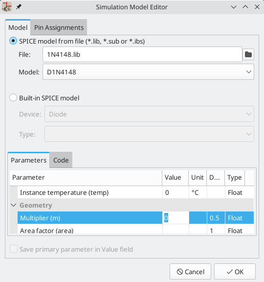
File is the path to the model file to use. Unencrypted model files are plain, human-readable text files and often have extensions such as .lib, .sub etc., although KiCad will accept a valid model with any extension.
The path to the file can be absolute, or relative to the project folder. The path can also be relative to the value of SPICE_LIB_DIR if you have defined that path variable. If you enable the Embed File checkbox in the file browser, the library file will be embedded in the schematic (or symbol library). This makes the schematic (or schematic) more portable as it doesn’t rely on an external library file. The library filename is saved in the symbol’s Sim.Library field.
Model is the name of the desired model in the model file. A model file may contain multiple models, and if so they will all be shown in the list. You can filter the list of models using the search box. The selected model is listed in the symbol’s Sim.Name field.
Parameters can be overridden (or additional parameters specified) using the Parameters tab. For device models, all parameters for that type of device are editable. For subcircuit models, any parameters included in the subcircuit definition are editable. Any parameters that are overridden in the Parameters tab are stored in the symbol’s Sim.Params field.
The Code tab displays the generated SPICE model as it will be written to the SPICE netlist for simulation.
| KiCad is not distributed with SPICE models for specific commercial devices. These models are usually available from device manufacturers or other internet sources. |
IBIS models
IBIS (I/O Buffer Information Specification) files are an alternative to SPICE models for modeling the behavior of input/output buffers on digital parts. In order to load an IBIS file, users should follow the procedure for SPICE library models, but provide a .ibs file.
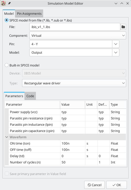
File is the path to the model file to use. The path can be absolute or
relative to the project folder. The path can also be relative to the value of
SPICE_LIB_DIR if you have
defined that path variable.
The library filename is saved in the symbol’s Sim.Library field. If an IBIS
model file is loaded, the remaining fields in the dialog will relate to the IBIS
model.
Component selects which component from the IBIS file to use, as IBIS files
can contain multiple components. The component name is saved in the symbol’s
Sim.Name field.
Pin selects which pin in the IBIS model to simulate. The selected pin must
be mapped to a symbol pin in the Pin Assignments tab. The chosen pin’s
number is saved in the symbol’s Sim.Ibis.Pin field.
Model is the list of models available for the selected pin, for example an
input or an output. The chosen model name is saved in the symbol’s
Sim.Ibis.Model field.
Type selects what the pin should do in the simulation. A pin can be a passive
device that doesn’t drive any value; it can be a DC driver that drives
high, low, or high-impedance; or it can be a rectangular wave or
PRBS driver. This value is stored in the symbol’s Sim.Type field.
The Parameters tab lets you see and edit the parameters of the model. For each parameter, you can switch between a minimum, typical, or maximum value, as defined in the IBIS file. You can also choose the parameters of the driven waveform, depending on the pin’s chosen type. Any parameters that differ from the defaults are stored in the symbol’s Sim.Params field.
| KiCad does not ship with IBIS models for symbols. IBIS models are usually available from device manufacturers. |
KiCad’s Simulation_SPICE symbol library provides several symbols that may be useful for IBIS simulations. IBIS_DEVICE can be used for device (input) pins, while IBIS_DRIVER can be used for simulating driver pins. There are also variants of each for differential pins.
|
Pin Assignment
Simulation models may have their pins numbered differently than the corresponding symbol. For example, SPICE models for diodes usually consider pin 1 to be the anode, while schematic symbols are usually drawn with pin 1 as the cathode. Operational amplifier models are also very likely to have model pin assignments that do not match package or schematic pin numbers.
You can use the Simulation Model Editor’s Pin Assignments tab to map the symbol’s pins to the simulation model pins.
| Always make sure symbol pins are correctly mapped to simulation model pins. Mistakes here can lead to erroneous or confusing simulation results, or a failure to simulate at all. |
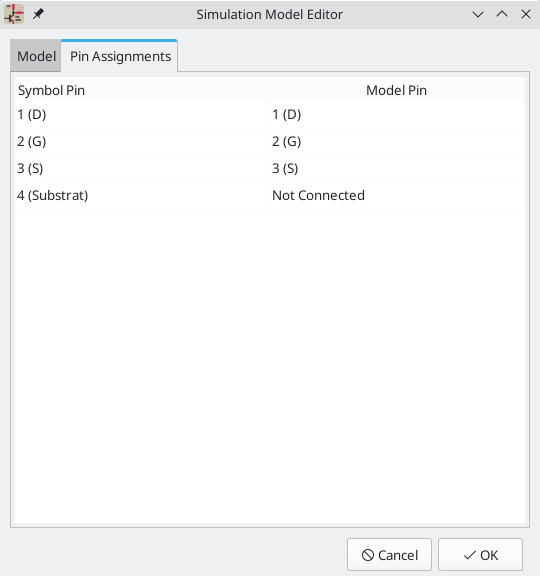
The left column displays the name and number of each symbol pin, i.e. the pin numbers and names that appear on the schematic part in KiCad. The right column displays the corresponding pin as defined in the model file in use. For each symbol pin, you can select the corresponding pin from the simulation model in the dropdown in the right column. In the cases where a schematic part has pins that are not in the model, as in the case of an operational amplifier with 'nulling' pins that are not modeled, the schematic part pin may be assigned to the 'Not Connected' option in the Pin Assignments dropdown. Unlike other pin assignments, 'Not Connected' may be assigned to multiple pins if necessary.
When you use a subcircuit model, the dialog displays the model’s code under the pin assignments for use as a reference while assigning pins. A well-written model will often include a helpful reference section (as a set of comments) to inform the user how the model pins are mapped.
Value notation
The simulator supports several notations for writing numerical values in simulation model parameters, simulation analysis setup options, and SPICE directives:
-
Plain notation :
10100,0.003, -
Scientific notation:
1.01e4,3e-3, -
Prefix notation:
10.1k,3m. -
RKM notation:
4k7,10R.
You can mix prefix and scientific notations. As such, 3e-4k is a valid input and is equivalent to 0.3. The list of valid prefixes is shown below. They are case sensitive.
| Prefix | Name | Multiplier |
|---|---|---|
a |
atto |
10-18 |
f |
femto |
10-15 |
p |
pico |
10-12 |
n |
nano |
10-9 |
u |
micro |
10-6 |
m |
milli |
10-3 |
k |
kilo |
103 |
M |
mega |
106 |
G |
giga |
109 |
T |
tera |
1012 |
P |
peta |
1015 |
E |
exa |
1015 |
Raw SPICE Element models and directives are passed to ngspice directly, without KiCad reformatting the values for ngspice to consume. ngspice uses a different, case-insensitive notation: 1 mega (106) is denoted there as 1Meg, while 1M is 1 milli (10-3). Depending on the compatibility mode selected, ngspice may not support the same value notations as KiCad, so care should be taken when using raw SPICE elements and simulation directives.
|
SPICE directives
It is possible to add SPICE directives by placing them in text fields on a schematic sheet. This approach is convenient for defining the default simulation type. The list of supported directives in text fields is:
-
Directives starting with a dot (e.g.
.tran 10n 1m) -
Coupling coefficients for inductors (e.g.
K1 L1 L2 0.89)
It is not possible to place additional components using text fields.
If a simulation command is included in schematic text, the simulator will use it as the simulation command when you open the simulator. However, you can override it by choosing a different simulation type in the Simulation Command dialog. You can also specify simulation commands with raw SPICE commands by using the Custom analysis type.
Refer to the ngspice documentation for more details about SPICE directives.
Running simulations
Circuits for simulation are drawn in the Schematic Editor, but simulations are run in the Simulator window.
After creating a schematic for simulation, the following steps are needed to run a simulation:
-
Open the simulator window by clicking Inspect → Simulator in the Schematic Editor or using the
 button in the top toolbar.
 -
Create at least one analysis by clicking Simulation → New Analysis Tab… (Ctrl+N) or using the
 button. This lets you choose a type of simulation and configure its options. These options are explained below. Each analysis has its own tab, and multiple analyses can be created. The options for an analysis can be adjusted after it is created with Simulation → Edit Analysis Tab… or by clicking on the
  button.
 -
Run the simulation by clicking Simulation → Run Simulation (R) or by clicking the
 button. This only runs the simulation in the active analysis tab. You can stop a running simulation at its current point by clicking the
  button.
 -
Examine the simulation results. Most analyses result in plots; for these you will need to select the signals to be plotted. Other analyses print their results in the output log window.
| Once a simulation has been set up, the configuration can be saved in a workbook. |
Simulator window
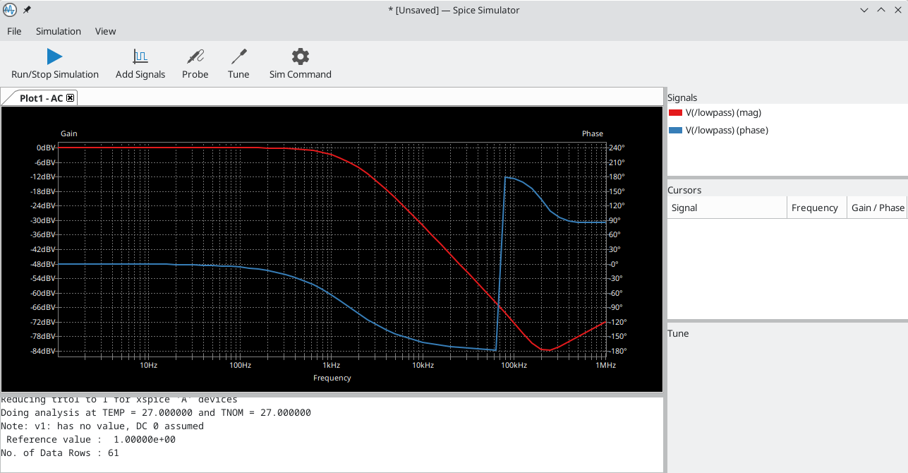
The simulator window is divided into several sections:
-
The top of the window has a toolbar with buttons for commonly used actions.
-
The main part of the window graphically shows the simulation results. The simulation needs to run and signals need to be selected from the list of available signals or probed before they are displayed in the plot.
-
Below the plot panel, the output log window shows logs from the ngspice simulation engine. Some types of analyses print their results here.
-
The right side of the window displays a list of signals, a list of active cursors, measurements, and a tuning tool for adjusting component values based on simulation results.
Simulation types
Each simulation is a specific type of analysis. The following analysis types are available:
Each analysis type and its options are explained below. You can configure an analysis when you create it (![]() button) or by editing an existing analysis (
button) or by editing an existing analysis (![]() button). These analysis types are explained in more detail in the ngspice documentation.
button). These analysis types are explained in more detail in the ngspice documentation.
| Another way to configure a simulation is to type SPICE directives into text fields on schematics. Any text field directives related to a simulation command are overridden by the settings selected in the dialog. This means that once a simulation has run, the dialog overrides the schematic directives until the simulator is reopened. |
Operating point analysis (OP)
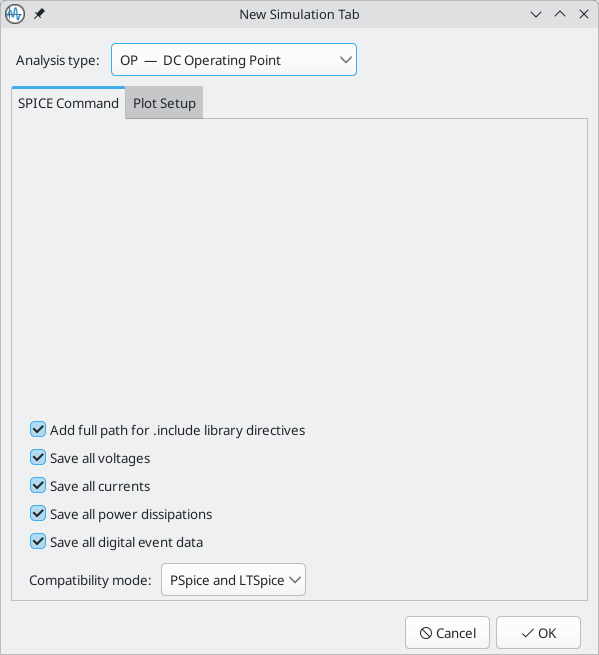
Calculates the DC operating point of the circuit. This analysis has no options.
Operating point analyses do not have any plotted results. Results are printed in the output log window. You can also display the node voltages and device currents calculated by this analysis as annotations in the schematic.
DC sweep analysis (DC)
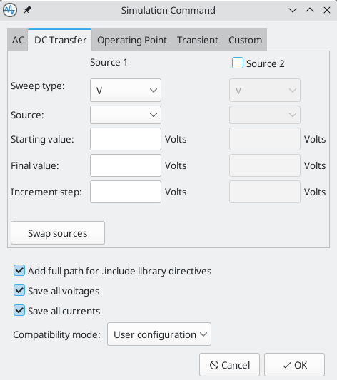
Calculates the DC behavior of the circuit while sweeping one or two parameters. The following parameters can be swept:
-
value of an independent voltage source
-
value of an independent current source
-
value of a resistor
-
simulation temperature
DC analyses have the following options, which are listed here with the corresponding ngspice parameter name:
-
Sweep type: the type of variable to sweep. This can be a voltage source, a current source, a resistor, or the simulation temperature.
-
Source: the particular voltage source, current source, or resistor to sweep (
srcnam). The list is populated with each item in the schematic of the relevant type. It is disabled for temperature sweeps. -
Starting value: the starting value for the sweep (
vstart). -
Final value: the ending value for the sweep (
vstop). -
Increment step: the amount to increase the value at each step of the sweep (
vincr). Smaller increments result in more output points.
If Source 2 is enabled, the same options are available to simultaneously sweep a second source. When sweeping two sources, Source 1 is swept over its entire range for each value of Source 2. In other words, each value for Source 2 results in a separate curve, and each curve shows a full sweep of Source 1 with Source 2 held constant at a particular value.
Clicking the Swap sources buttons swaps Source 1 with Source 2.
The output is displayed as a plot.
| The tuning tool is another way to see how component values affect circuit behavior. Unlike DC sweeps, the tuning tool can be used with other types of simulations, like transient or AC analyses. |
AC small-signal analysis (AC)
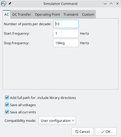
Calculates the small-signal AC behavior of the circuit in response to a stimulus. Performs a decade sweep of stimulus frequency.
To run an AC analysis you must choose a number of points to measure per decade and the start and end frequencies for the decade sweep.
AC analyses have the following options, which are listed here with the corresponding ngspice parameter name:
-
Number of points per decade: the number of points to calculate per decade (
nd). -
Start frequency: the lower bound of the frequency range to analyze (
fstart). -
Stop frequency: the upper bound of the frequency range to analyze (
fstop).
The output is displayed as a Bode plot (output magnitude and phase vs. frequency).
Transient analysis (TRAN)
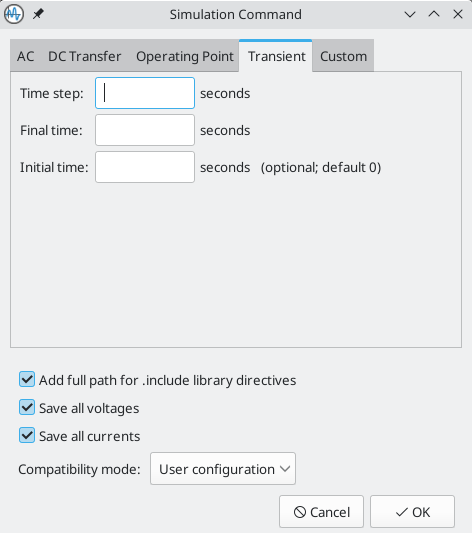
Calculates the time-varying behavior of the circuit.
Transient analyses have the following options, which are listed here with the corresponding ngspice parameter name:
-
Time step: a suggested time step (
tstep). -
Final time: the time at which the simulation will end (
tstop). -
Initial time: the time at which the simulation will start (
tstart). If not specified, this defaults to 0. -
Max time step: the maximum time step (
tmax). If not specified, this defaults to the suggested time step or the total simulation duration divided by 50, whichever is smaller. -
Use initial conditions: if enabled, the simulator will not calculate the quiescent operating point before starting the transient simulation. Instead, the simulation will use the initial conditions specified in a
.icdirective and elementICparameters. This corresponds to ngspice’suicoption.
The output is displayed as a plot.
Pole-zero analysis (PZ)
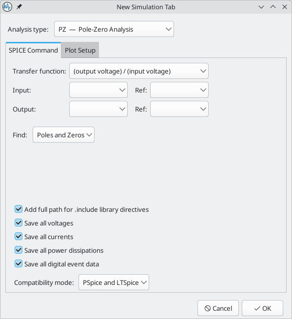
Calculates the poles and zeroes of the small-signal (AC) transfer function of the circuit.
Pole-zero analyses have the following options, which are listed here with the corresponding ngspice parameter name:
-
Transfer function: selects between calculating the transfer function as output voltage divided by input voltage or output voltage divided by input current. These correspond to ngspice’s
volandcuroptions, respectively. -
Input: the input node (
node1) and the reference node for the input (node2). -
Output: the output node (
node3) and the reference node for the output (node4). -
Find: selects between calculating poles and zeroes, only poles, or only zeroes. These correspond to ngspice’s
pz,pol, andzeroptions, respectively.
Operating point analyses do not have any plotted results. Results are printed in the output log window.
Noise analysis (NOISE)
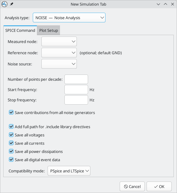
Calculates the noise generated by the devices in the circuit, both as output noise and input-referred noise. The noise spectrum (V/√Hz or A/√Hz) of the circuit can be plotted, and the total noise over the specified frequency range is reported. Optionally, the noise contributions of each device are reported individually.
Noise analyses have the following options, which are listed here with the corresponding ngspice parameter name:
-
Measured node: the node at which output noise is measured (
output). -
Reference node: the reference node for measuring the output noise (
ref). The output noise is calculated as the noise at the measured node minus the noise at the reference node. If it is not specified, the default is the ground node. -
Noise source: a source that is considered the circuit’s input for the purposes of calculating input-referred noise (
src). The source must specify an AC magnitude, i.e. the source must have anacparameter. -
Number of points per decade: the number of points to calculate per decade (
pts). -
Start frequency: the lower bound of the frequency range to analyze (
fstart). -
Stop frequency: the upper bound of the frequency range to analyze (
fstop). -
Save contributions from all noise generators: if enabled, noise magnitudes of individual noise generators are saved and reported. If disabled, only the overall output and input-referred noise over the specified frequency range are reported.
The output and input-referred noise spectra can be plotted. Total noise values for the specified frequency range are printed in the output log window.
S-parameter analysis (SP)
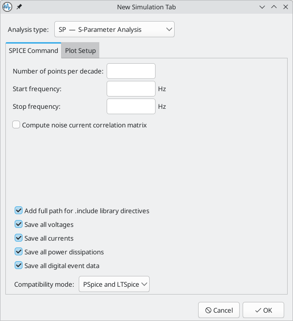
Calculates the scattering parameters, admittance matrix, and impedance matrix for the circuit. Optionally calculates the noise current correlation matrix. Note that this analysis requires at least two voltage sources configured as RF ports as described in the ngspice manual.
S-parameter analyses have the following options, which are listed here with the corresponding ngspice parameter name:
-
Number of points per decade: the number of points to calculate per decade (
nd). -
Start frequency: the lower bound of the frequency range to analyze (
fstart). -
Stop frequency: the upper bound of the frequency range to analyze (
fstop). -
Compute noise current correlation matrix: if enabled, the noise current correlation matrix is also calculated. This corresponds to ngspice’s
donoiseoption.
The output is displayed as a plot.
Frequency content analysis (FFT)
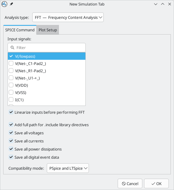
Calculates an FFT based on an existing analysis tab. Any of the signals from an existing analysis can be used as inputs to the FFT. The signals are windowed using a Hanning window.
FFT analyses have the following options, which are listed here with the corresponding ngspice parameter name:
-
Input signals: the signal(s) to perform an FFT on. An FFT is independently applied to each selected signal.
-
Linearize inputs before performing FFT: When enabled, the input vector is converted to have equidistant time points prior to performing the FFT. Corresponds to ngspice’s
linearizecommand.
The output is displayed as a plot.
Custom analysis
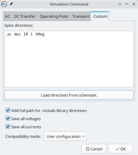
Performs a SPICE analysis defined by raw SPICE analysis commands (.tran, .ac, .dc, .noise, etc.). For details on such analysis commands and their syntax, refer to the ngspice documentation.
The analysis commands given on each line of the SPICE directives textbox are run as separate analyses. If you click the Load Directives from Schematic button, any SPICE directives in schematic text are copied into the textbox.
Additional simulation settings
There are several simulation options that apply to all types of simulations. These are located at the bottom of the dialog.
-
Add full path for .include library directives: if enabled, relative paths to SPICE models will be converted to absolute paths in the SPICE netlist.
-
Save all voltages: if enabled, the simulator will save voltages for each node in the simulation results so that they can be plotted. This corresponds to ngspice’s
.save allcommand in the SPICE netlist. If disabled, voltages will not be saved in the results, and therefore cannot be plotted, unless a SPICE directive is used to manually probe a node voltage. -
Save all currents: if enabled, the simulator will save currents through each device pin in the simulation results so that they can be plotted. This corresponds to ngspice’s
.probe allicommand in the SPICE netlist. If disabled, currents will not be saved in the results, and therefore cannot be plotted, unless a SPICE directive is used to manually probe a current. -
Save all power dissipations: if enabled, the simulator will save power dissipations for each device in the simulation results so that they can be plotted. This corresponds to ngspice’s
.probe P(<device>)command in the SPICE netlist for each device in the schematic. If disabled, power dissipations will not be saved in the results, and therefore cannot be plotted, unless a SPICE directive is used to manually probe a power dissipation. -
Save all digital event data: if enabled, the simulator will save digital event data for digital (event-driven) simulation models. This corresponds to ngspice’s
.esave allcommand. If disabled, digital event data will be discarded. -
The Compatibility mode dropdown selects the compatibility mode that the simulator uses to load models. The User configuration option refers to the user’s
.spiceinitngspice configuration file. Compatibility modes are described in the ngspice documentation.
Viewing simulation results
Each analysis has its own tab, containing its own separate plot, signal list, and output log window. Only the active tab is updated when a simulation is run. In this way it is possible to compare simulation results between different runs.
Simulation results from most analysis types are visualized as plots. However, DC Operating Point (OP) and Pole-zero (PZ) analyses do not generate plots. Instead, they print their results in the output log at the bottom of the simulator window. OP analysis results can additionally be displayed as annotations on the schematic canvas.
Plotted results
Most types of analyses display their results in a plot. The type of plot depends on the analysis: transient simulations display signal values over time, for example, while AC simulations display results in a Bode plot.
You can zoom and move a plot using the following gestures:
-
Scroll mouse wheel to zoom in/out. Shift, Ctrl, and Alt can modify the scroll action depending on the configuration in the Simulator panel in the Schematic Editor Preferences.
-
Right click to open a context menu to adjust the view.
-
Draw a selection rectangle to zoom in the selected area.
-
Drag a cursor marker to move the cursor.
The list of signals that can be plotted in the active plot is shown in the Signals pane on the right side of the simulator window. The following types of signals can be plotted:
-
Node voltages: the voltage of each net in the schematic, displayed as
V(<net>). -
Device node currents: the current for each device in the schematic, displayed as
I(<device>)orI(<device:terminal>). For two-terminal devices, the device’s current is listed as a single signal corresponding to the current into the device’s pin 1. For devices with more than two terminals, the current into each terminal is a separate signal. -
Device power dissipations: the power dissipated by each component, displayed as
P(<device>). -
User-defined signals: custom signals defined as an expression based on other signals. User-defined signals can be arbitrary mathematical expressions. One common use for user-defined signals is to plot a voltage differential, i.e. the voltage between two points.
To plot a signal, check the box in the plot column next to the signal of interest. To remove a signal from the plot, clear its checkbox.
You can also interactively select signals to plot by using the Probe Schematic tool. To activate the tool, use Simulation → Probe Schematic… (P) or click the (![]() ) button. When activated, the tool lets you click elements in the schematic to plot the corresponding signal. Different types of signals are probed depending on what you click:
) button. When activated, the tool lets you click elements in the schematic to plot the corresponding signal. Different types of signals are probed depending on what you click:
-
Clicking on a wire plots the voltage of that net. When you hover over a wire, the net is highlighted to indicate that its voltage can be probed.
-
Clicking on a symbol pin plots the current going into that pin. When you hover over a pin, the cursor changes to a current clamp to indicate that clicking will probe the current.
KiCad does not support ngspice’s .plot directive. This directive has no
effect when a simulation is run using KiCad.
|
Plot settings and appearance
Colors of individual signals may be set by clicking the color field associated with each signal in the Signals grid. You may choose from a predefined palette (Defined Colors), or select a custom color (Color Picker). You can toggle the color of the plot background from black to white with View → Dark Mode Plots (this affects all analysis tabs, not just the active tab).
Many plot settings can be configured in the Plot Setup tab of the Analysis Setup window (![]() button).
button).
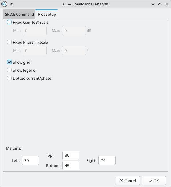
-
Fixed scale: when enabled, this fixes the vertical and/or horizontal plot scales to the specified ranges. Manually zooming will not affect an axis if its scale is fixed.
-
Show grid: when enabled, a grid will be shown behind the plotted signals. You can also turn the grid on or off with View → Show Grid.
-
Show legend: when enabled, a legend will be shown on the plot for the enabled signals. You can reposition the legend by dragging it.
-
Dotted current/phase: when enabled, plotted signals representing current (transient simulations) or phase (AC simulations) are displayed using dotted lines instead of solid lines. You can also enable this setting with View → Dotted Current/Phase.
-
Margins: this controls the padding on each side of the plot.
Cursors
For precise measurement, cursors are available in the plot window. You can add a cursor to a signal by checking the Cursor 1 or Cursor 2 checkbox for the signal in the signal grid on the right. Each cursor always tracks its signal: the intersection of the cursor’s horizontal and vertical lines is always exactly on the signal.
Once cursors have been added, the horizontal position of each cursor is shown by a number in a triangular marker at the top of the plot display. You can reposition each cursor by clicking and dragging its marker. The vertical position of each cursor tracks its assigned signal. The horizontal and vertical value for each cursor are shown in the cursor grid on the right of the simulator window. If cursors 1 and 2 are both enabled, the difference between them is also shown.
When you are tuning in Multi Run mode, and multiple curves are plotted for each signal, you can move a cursor from one plotted curve to another curve of the same signal by dragging it with the mouse. The cursor will follow the plotted curve that is closest to the mouse position.
To precisely position a cursor, you can directly edit its horizontal position in the cursors grid. You can also modify the display format (unit range and number of significant digits) by right clicking a value in the cursors grid and clicking Format for the relevant quantity.
You can also add more cursors beyond the two default cursors. To create more cursors, right click on a signal in the signals grid and click Create new cursor. To remove an extra cursor, right click in a one of the extra cursor columns and click Delete cursor 3 (or whichever cursor you want to delete).
Measurements
You can add automatically calculated measurements for any plotted signal, such as a minimum, average, or peak-to-peak measurement.
| Measurements are made over all the data resulting from the simulation, not just the data that is visible in the plot window at the current zoom setting. |
| It is not necessary to have selected a signal for plotting (by selecting its Plot checkbox) in order to make a measurement on it. Even unplotted signals can be measured. |
To add a predefined measurement to a signal, right click on a signal in the signals grid and select a measurement. The following measurements are available:
-
Measure Min: measures the minimum value of the entire signal
-
Measure Max: measures the minimum value of the entire signal
-
Measure RMS: measures the root-mean-square value of the entire signal
-
Measure Peak-to-peak: measures the peak-to-peak value of the entire signal
-
Measure Time of Min: measures the time at which the minimum value of the entire signal occurs
-
Measure Time of Max: measures the time at which the maximum value of the entire signal occurs
-
Measure Integral: computes the time integral value of the entire signal
-
Perform Fourier Analysis: performs a Fourier analysis of the selected signal based on a specified fundamental frequency. Calculates the amplitude of the harmonics of the fundamental as well as the total harmonic distortion. This measurement is only available for transient analyses, and its results are printed in the simulation log window instead of in the measurement panel.
Measurement results are displayed in the Measurement pane at the lower right of the simulator window. Multiple measurements will display as multiple rows in this area. You can delete a measurement by right clicking it and clicking Delete Measurement. To modify the display format of a measurement result (unit range and number of significant digits), right click the value and click Format Value….
The above context menu options are a shortcut for directly specifying measurements in the the Measurement pane. To manually create a new measurement, click in an empty row in the Measurement pane and type in an ngspice measurement function. You can also edit existing measurements by clicking on them. For more information about measurements and their syntax, refer to the ngspice manual.
Numerical results
While most analyses display their results as plots, DC Operating Point (OP) and Pole-zero (PZ) analyses do not result in plots. Instead, these analyses print their results as text in the simulation log window.
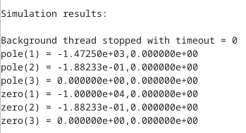
Operating point annotations
For the OP analysis, annotations can also be added to the schematic indicating the operating point voltage and current values at the nodes. Operating point voltage annotations can be shown or hidden for every node with View → Show OP Voltages. Operating point current annotations can be shown or hidden for every symbol pin with View → Show OP Currents. These annotations are globally shown or hidden for every node or every pin. You can control the formatting of these annotations in the Formatting panel of Schematic Setup.
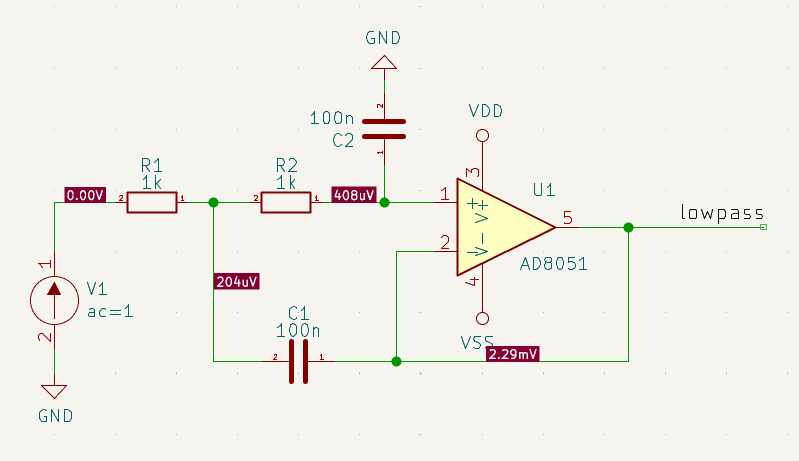
You can also display operating point results using text variables. Using text variables requires more work to set up but provides more control over how the data is displayed. For example, you can use text variables to display only certain voltages or currents, or to control the display formatting of particular values. You can also use text variables to display power dissipation measurements.
To use text variables to display an operating point voltage for a net, add a label to the net, then add a field to that label. The label can contain any text as long as it contains the ${OP} text variable. The text variable can contain formatting specifiers in the form ${OP.<precision><unit>}, but both the precision and unit are optional. Precision is the number of significant digits to display, which is 3 by default. Unit is the unit to use, including a prefix, such as mV for millivolts.
As an example, a label field containing the text Vout: ${OP}, attached to a net with an operating point voltage of 5.123V, displays as "Vout: 5.12V". The text ${OP.4mV} displays as "5123mV", ${OP.2} displays as "5.1V", and ${OP.mV} displays as "512mV".
Using text variables to display an operating point current into a device pin is similar, but uses symbol fields instead of label fields. The field can contain any text as long as it contains the ${OP:<pin>} text variable. The pin can be specified as a pin name or a pin number. For two-terminal devices, the pin can be omitted, and the current into the device’s pin 1 will be reported. The same optional formatting specifiers are supported as for voltages, in the form ${OP:<pin>.<precision><unit>}.
For example, in a symbol with an operating point current of 5.123mA through pin 1 (pin name C), a symbol field containing the text Ic: ${OP:C} displays as "Ic: 5.12mA". The text ${OP:C.2mA} displays as "5.1mA", ${OP:1.4} displays as "5.123mA", and ${OP:C.A} displays as "0.00512A".
You can also use text variables to display a device’s power dissipation. This works identically to current, but with power instead of a pin name or number. For example, in a symbol with an operating point power dissipation of 5.123mW, a symbol field containing ${OP:power.2mW} displays as "5.1mW".
| Don’t forget to set the label field or symbol field to visible, or it will not be displayed. |
User-defined signals
In addition to the list of signals that come from the nets in the schematic, you can define your own signals which behave like normal signals in most respects. User defined signals are defined as mathematical operations on one or more basic signals.
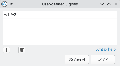
To add a user-defined signal, open the User-defined Signal dialog with Simulation → User-defined Signals… (![]() button) and add a signal. The new signal will appear in the Signal grid, where it can be plotted and used like any other signal. User-defined signals are also included in OP results.
button) and add a signal. The new signal will appear in the Signal grid, where it can be plotted and used like any other signal. User-defined signals are also included in OP results.
| Unlike normal signals, which are plotted incrementally as a simulation progresses, user-defined signals are not plotted until the simulation completes. |
One use for user-defined signals is to plot a differential voltage, i.e. the voltage between two arbitrary nodes. For example, to plot the voltage difference between the nets /v1 and /v2, you can create a user-defined signal with the expression /v1-/v2 and then plot it. This expression could also be written in a number of different ways, for example V(/v1)-V(/v2) or V(/v1,/v2), which are both equivalent.
A number of mathematical functions are available for use in user-defined signals. To see a list, click the Syntax help link in the User-defined Signals dialog. Refer to the ngspice manual for details on each of these functions.
Net names may contain special characters that have particular meaning to
the ngspice interpreter. In particular, ngspice interprets the dash
character (-) as a subtraction operation. To ensure that net names are
interpreted correctly, surround the net name with double quote (")
characters when referring to it in a user-defined signal.
|
Tuning components
The simulator has a tuning tool, which lets you observe how changing a component value affects the simulation results. Each time the component value is tuned, the simulation is re-run with the new component value. You can then save the tuned component value back to the schematic if desired.
The following components can be tuned:
-
Resistors
-
Inductors
-
Capacitors
-
DC Voltage sources
-
DC Current sources
| You can only tune components when running analyses that result in a plot. In other words, you cannot tune components when running an operating point analysis. |
To tune a component, use Simulation → Add Tuned Value…, the keyboard shortcut T, or the ![]() button in the toolbar, and then click on the component to tune in the schematic. This adds a tuning control for that component in the bottom right corner of the simulator window. Multiple components can be tuned at once, with a separate tuning control per component.
button in the toolbar, and then click on the component to tune in the schematic. This adds a tuning control for that component in the bottom right corner of the simulator window. Multiple components can be tuned at once, with a separate tuning control per component.
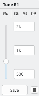
-
The dropdown menu at the top switches between Single Run and Multi Run modes.
-
In Single Run mode, the simulation is run using the tuned value from the middle text field. Each time this value changes, the simulation is re-run with the new value, and the new results replace the old results.
-
In Multi Run mode, the simulation is run multiple times using different values for the tuned value. All runs are plotted simultaneously to show the spread of results. The Steps control sets the number of runs. The minimum is two runs, as the minimum and maximum values of the tuning range are always included.
-
-
The top text field sets the top end of the tuning range. In Multi Run mode, this sets the value for the last simulation run.
-
The bottom text field sets the bottom end of the tuning range. In Multi Run mode, this sets the value for the first simulation run.
-
The middle text field sets the actual component value that is used in the simulation in Single Run mode. This value can also be adjusted using the slider. In Multi Run mode, the middle text field is disabled.
-
The Save button updates the schematic symbol with the tuned value. Until you press the Save button, the schematic symbol will keep its original value. In Multi Run mode, the Save button is disabled because there is no single value to save back to the schematic.
-
The
 button removes the component from the Tune panel and restores its original value.
In addition, it is possible to restrict the component values to those from a particular series of Preferred Values — either of the E24, E48, E96 or E192 series. This is particularly useful when it is necessary to restrict component values to commercially available parts.
Saving simulation setups
You can save a simulation setup in a workbook. Workbooks are files that store information about a simulation setup, including which analyses are configured and what their settings are, which signals are plotted for each analysis, user-defined signals, measurements, cursors, and display settings. A workbook can be saved and reloaded later to restore the previously configured settings in a new session. Workbooks can include more than one simulation: for example, it may contain separate tabs for transient, operating point, and AC analyses which you added as you worked.
You can save a workbook using File → Save Workbook and load one using File → Open Workbook. The most recently used workbook is automatically loaded when the simulator is opened.
| Workbooks store simulation setup information, but they do not store simulation results. You can export simulation results to PNG (graphics) or CSV (simulation data values) with File → Export Current Plot as PNG… and File → Export Current Plot as CSV…. To recreate the results of simulations stored in a workbook, select the appropriate analysis tab in the Simulator window and run the simulation again (R or Simulation → Run Simulation). |
Exporting simulation results
KiCad’s simulator offers two ways to export results:
-
as a PNG (Portable Network Graphics format) image of a simulation data plot,
-
as a plain text file of simulation data values, in CSV (Comma-Separated Value) format.
Only simulations that produce plots (see above) can be exported as an image or a CSV file. The results of OP and PZ analyses cannot be exported in this way.
Exporting results as graphics
The currently-visible Simulator plot may be exported as a PNG file using the command File → Export Current Plot as PNG….
The size and aspect-ratio of the saved image will match that of the displayed plot in the Simulator.
You can also copy an image of the active plot to the clipboard using File → Export Current Plot to Clipboard, or insert an image of the active plot into the schematic using File → Export Current Plot to Schematic. Exporting a plot to the schematic is equivalent to exporting the plot to the clipboard and then pasting it into the schematic.
Exporting results as numerical data
The currently-visible Simulator plot may be exported as a CSV file using the command File → Export Current Plot as CSV….
The data in the simulation plot is exported as multiple columns. The precise format is dependent upon the analysis type. In general, there will be multiple columns of data, one corresponding to each variable selected for plotting. The first row of the file is a header row, containing the name of the variable in the column (i.e. 'time', 'V(/Vout)1' or similar).
| When exporting to CSV, only variables selected using their Plot checkbox will be included in the exported file. |
| The data in the exported file contains all the data that would be plotted if the entire plot were displayed. If the plot is zoomed in to show a particular region this will still be the case, resulting in the output file containing more data than the user might expect. |
This function exports the data with data separated by semicolons (;) rather than commas. Programs reading this data may need to be configured to expect a semicolon as a delimiter.
|
Troubleshooting simulations
Sometimes a simulation will fail, either with or without errors being reported. Paying attention to the error messages reported, taking care in the development and entry into KiCad of the circuit to be simulated, and making use of the KiCad, ngspice and general SPICE documentation and information from fellow users in forums is very worthwhile and can often point the way to a solution.
It’s worth noting, for users unfamiliar with SPICE, ngspice or circuit simulation in general that some 'common' and interesting circuits can sometimes be tricky to simulate accurately or reliably. These include apparently simple circuits such as oscillators, which in some cases may fail to oscillate at all! It is nearly always possible to build a working simulation but sometimes this can more require SPICE experience than might be initially apparent, or the guidance of someone who already has it. The ngspice documentation, once again, is worth reading for insights into good and effective simulation practices if you are encountering difficulty.
Incorrect netlist
It is possible to inspect the SPICE netlist with Simulation → Show SPICE netlist… (![]() button). This method of troubleshooting requires some SPICE knowledge, but spotting errors in the netlist can help determine the cause of simulation problems, as well as providing confirmation of what input ngspice is actually acting on.
button). This method of troubleshooting requires some SPICE knowledge, but spotting errors in the netlist can help determine the cause of simulation problems, as well as providing confirmation of what input ngspice is actually acting on.
Simulation error messages
The output console displays messages from the simulator. It is advisable to check the console output to verify there are no errors or warnings. Messages appearing in the console may be conveniently selected, copied, and pasted if you wish to share them.
A common error message is "timestep too small". This message means that the simulation engine is unable to calculate the next point in the simulation, even when using the minimum possible time increment. This error can have many causes, including numerical convergence issues with a simulation model used in the circuit or with the circuit itself. It can also be caused by mistakes in drawing the circuit, such as incorrectly assigning pins to the simulation model or forgetting to provide a voltage supply.
Convergence problems
In case the simulation does not converge in a reasonable amount of time (or not at all), it is possible to add the following SPICE directives. More information is available in the ngspice manual.
| Changing convergence options can lead to erroneous results. These options should be used with caution. |
.options gmin=1e-10
.options abstol=1e-10
.options reltol=0.003
.options cshunt=1e-15
-
gminis the minimum conductance allowed by the program. The default value is1e-12(1 pS). -
abstolis the absolute current error tolerance of the program. The default value is1e-12(1 pA). -
reltolis the relative error tolerance of the program. The default value is0.001(0.1%). -
cshuntadds a capacitor of the specified value from each voltage node in the circuit to ground.
Simulation pin assignments
If unexpected results are generated by a simulation despite it running without obvious errors, it is worth double-checking that the assignments between the pins of the part instance in the KiCad schematic and that of the associated model are correct. These have to be correct for each instance of the model in the schematic.
Helpful hints
Some helpful tips, hints and advice to help you get the most from using ngspice in KiCad for simulation.
The ngspice manual is your friend!
Fundamentally the KiCad Simulator is a user-friendly front-end to the powerful ngspice circuit simulator. Therefore problems with the details of simulation, the correct use of SPICE elements, models, etc. is beyond the scope of the KiCad documentation but is very likely to be fully and completely addressed in the ngspice documentation itself. It’s therefore recommended not to overlook this valuable resource.
| KiCad updates may result in changes to the ngspice version used by the simulator. The current version of ngspice used in a particular version of KiCad is shown on the Help → About KiCad dialog, under the Version tab. Referring to the online ngspice documentation will ensure you always have access to the latest information for reference. |
Organizing third-party models
Although it is certainly possible to keep simulation models (i.e. .lib, .sub files) in the directories associated with individual KiCad projects, this will likely result in unnecessary copies of model files proliferating as you create simulations. Consider creating a dedicated storage location (directory, folder) for models, perhaps organized by manufacturer or device type, to hold these files. Then they may simply be referenced in simulations at a common location.
Simulation symbols and models in KiCad’s libraries
The KiCad libraries provide a number of symbols for simulation in the Simulation_SPICE symbol library. Most of these symbols have SPICE models already assigned as appropriate, although you may need to adjust the model parameters in order to obtain the desired simulation behavior.
The Simulation_SPICE symbol library contains the following symbols:
Symbol Name |
Descripción |
0 |
A ground (node 0) symbol. Note that a standard GND symbol from another library can also be used. |
BSOURCE |
A symbol for a SPICE B-source (nonlinear dependent voltage or current source). Refer to the ngspice manual for information on B-sources. |
D |
A diode symbol. Note that the pin assignment is appropriate for both simulation and PCB layout. |
ESOURCE |
A symbol for a SPICE E-source (linear voltage-controlled voltage source). By default it is set up with a gain of 1 V/V. Refer to the ngspice manual for more information on E-sources. |
GSOURCE |
A symbol for a SPICE G-source (linear voltage-controlled current source). By default it is set up with a gain of 1 A/V. Refer to the ngspice manual for more information on G-sources. |
IAM |
A symbol for a SPICE amplitude-modulated independent current source. Refer to the ngspice manual for more information on independent current sources. |
IBIS_DEVICE |
An IBIS device symbol representing a digital input pin. This symbol is not preconfigured with a simulation model. It is intended to be used with an external IBIS model for a device. |
IBIS_DEVICE_DIFF |
An IBIS device symbol representing a digital differential input pin. This symbol is not preconfigured with a simulation model. It is intended to be used with an external IBIS model for a differential device. |
IBIS_DRIVER |
An IBIS driver symbol representing a digital output pin. This symbol is not preconfigured with a simulation model. It is intended to be used with an external IBIS model for a driver. |
IBIS_DRIVER_DIFF |
An IBIS driver symbol representing a pair of digital differential output pins. This symbol is not preconfigured with a simulation model. It is intended to be used with an external IBIS model for a differential driver. |
IDC |
A symbol for a SPICE DC independent current source. Refer to the ngspice manual for more information on independent current sources. |
IEXP |
A symbol for a SPICE exponential independent current source. Refer to the ngspice manual for more information on independent current sources. |
IPULSE |
A symbol for a SPICE pulsed independent current source. Refer to the ngspice manual for more information on independent current sources. |
IPWL |
A symbol for a SPICE piecewise linear independent current source. The waveform is specified as space-separated time-current pairs. Refer to the ngspice manual for more information on independent current sources. |
ISFFM |
A symbol for a SPICE single-frequency frequency-modulated independent current source. Refer to the ngspice manual for more information on independent current sources. |
ISIN |
A symbol for a SPICE sinusoidal independent current source. Refer to the ngspice manual for more information on independent current sources. |
ITRNOISE |
A symbol for a SPICE transient noise independent current source. Refer to the ngspice manual for more information on independent current sources. |
ITRRANDOM |
A symbol for a SPICE transient random independent current source. Refer to the ngspice manual for more information on independent current sources. |
NJFET |
A symbol for an N-channel JFET with drain, gate, and source terminals, suitable for use with 3-terminal N-JFET models. |
NMOS |
A symbol for an N-channel MOSFET with drain, gate, and source terminals, suitable for use with 3-terminal N-MOSFET models. |
NMOS_Substrate |
A symbol for an N-channel MOSFET with drain, gate, source, and substrate (bulk) terminals, suitable for use with 4-terminal N-MOSFET models. |
NPN |
A symbol for an NPN transistor with collector, base, and emitter terminals, suitable for use with 3-terminal NPN models. |
NPN_Substrate |
A symbol for an NPN transistor with collector, base, emitter, and substrate terminals, suitable for use with 4-terminal NPN models. |
OPAMP |
A generic single-pole operational amplifier symbol. There are parameters for pole frequency, open loop gain, offset voltage, and output resistance. These parameters can be edited in the Parameters grid of the SPICE Model Editor dialog. |
PJFET |
A symbol for a P-channel JFET with drain, gate, and source terminals, suitable for use with 3-terminal P-JFET models. |
PMOS |
A symbol for a P-channel MOSFET with drain, gate, and source terminals, suitable for use with 3-terminal P-MOSFET models. |
PMOS_Substrate |
A symbol for a P-channel MOSFET with drain, gate, source, and substrate (bulk) terminals, suitable for use with 4-terminal P-MOSFET models. |
PNP |
A symbol for a PNP transistor with collector, base, and emitter terminals, suitable for use with 3-terminal PNP models. |
PNP_Substrate |
A symbol for a PNP transistor with collector, base, emitter, and substrate terminals, suitable for use with 4-terminal PNP models. |
SWITCH |
A symbol for a voltage-controlled switch. Refer to the ngspice manual for more information on switches. |
TLINE |
A symbol for a transmission line. By default it is set up as a lossless transmission line but it can also be used for a lossy transmission line. Refer to the ngspice manual for more information on transmission lines. |
VAM |
A symbol for a SPICE amplitude-modulated independent voltage source. Refer to the ngspice manual for more information on independent voltage sources. |
VDC |
A symbol for a SPICE DC independent voltage source. Refer to the ngspice manual for more information on independent voltage sources. |
VEXP |
A symbol for a SPICE exponential independent voltage source. Refer to the ngspice manual for more information on independent voltage sources. |
VOLTMETER_DIFF |
A differential voltmeter symbol that can be used to measure the voltage
between two arbitrary nodes. The voltage difference between the |
VPULSE |
A symbol for a SPICE pulsed independent voltage source. Refer to the ngspice manual for more information on independent voltage sources. |
VPWL |
A symbol for a SPICE piecewise linear independent voltage source. The waveform is specified as space-separated time-voltage pairs. Refer to the ngspice manual for more information on independent voltage sources. |
VSFFM |
A symbol for a SPICE single-frequency frequency-modulated independent voltage source. Refer to the ngspice manual for more information on independent voltage sources. |
VSIN |
A symbol for a SPICE sinusoidal independent voltage source. Refer to the ngspice manual for more information on independent voltage sources. |
VTRNOISE |
A symbol for a SPICE transient noise independent voltage source. Refer to the ngspice manual for more information on independent voltage sources. |
VTRRANDOM |
A symbol for a SPICE transient random independent voltage source. Refer to the ngspice manual for more information on independent voltage sources. |
Most of these symbols in the Simulation_SPICE library use built-in models, but several symbols use external models from the Simulation_SPICE.sp simulation model library. The simulation model library is a separate file in the same folder as the symbol library. This simulation model library also contains SPICE models that may be useful for use with other symbols.
The Simulation_SPICE.sp simulation model library contains the following models:
Model Name |
Descripción |
kicad_builtin_opamp |
A generic single-pole operational amplifier model. This model is used by the
OPAMP symbol in the |
kicad_builtin_opamp_dual |
A dual version of the kicad_builtin_opamp model, with the same parameters.
This model is not assigned to any symbols in the |
kicad_builtin_opamp_quad |
A quad version of the kicad_builtin_opamp model, with the same parameters.
This model is not assigned to any symbols in the |
kicad_builtin_varistor |
A generic varistor model. This model is not assigned to any symbols in the
|
kicad_builtin_vdiff |
A differential voltmeter model. The voltage difference between the first two
terminals is output as a ground-referenced voltage on the third terminal.
This model is used by the VOLTMETER_DIFF symbol in the |
Advanced Topics
Configuration and Customization
| This section of the KiCad documentation has not yet been written. We appreciate your patience as our small team of volunteer documentation writers work to update and expand the documentation. |
Text variables
KiCad supports text variables, which allow you to reference predefined variables by name in many kinds of text. KiCad will substitute the variable name with the text string assigned to the variable. Text variables can be used in schematic and PCB graphic text, symbol and footprint text, symbol and footprint fields, drawing sheet fields, label names, label fields, hierarchical sheet fields, and other text contexts. This substitution happens anywhere the variable name is used inside the variable replacement syntax of ${VARIABLENAME}.
For example, you could create a variable named VERSION and set the text substitution to 1.0. Now, in any text object in the schematic, you can enter ${VERSION} and KiCad will display this as 1.0. If you change the value to 2.0, every text object that includes ${VERSION} will be updated automatically. You can also mix regular text and variables: a text object with the text Version: ${VERSION} will be displayed as Version: 1.0.
You can define project text variables in the schematic or board setup dialogs. These are referred to as project text variables because they are defined for the whole project, so a project text variable defined in the Schematic Editor can also be used in the Board Editor, and vice versa.
The Schematic Editor also has a number of built-in system text variables, which are listed in the table below. System text variables may be available in some contexts and not others. There is an equivalent list of variables for the PCB Editor.
Variables used in hierarchical sheet fields refer to the properties of the hierarchical sheet, not the parent, unless otherwise noted. For example, ${#} returns the subsheet’s page number when used in a hierarchical sheet field, but the parent sheet’s page number when used in graphic text in the parent sheet.
Variables can also be used for field names. A field with a variable as its name will automatically have its value set to the same variable. For example, in a project with a project variable MY_VAR set to MY_VALUE, a user-created symbol field named ${MY_VAR} will automatically have its value set to ${MY_VAR}, which will then resolve to MY_VALUE. If the field’s Show Name property is set, the variable’s name will be displayed as the field name, for example MY_VAR: MY_VALUE.
| Variable name | Descripción |
|---|---|
|
Sheet number. |
|
Total number of schematic sheets. |
|
Column (letter) and row (zero-indexed number) address of current table cell. This variable is only available in table cells. |
|
Contents of the table cell indexed by |
|
Column number (zero-indexed) of current table cell. This variable is only available in table cells. |
|
Contents of drawing sheet’s |
|
Contents of drawing sheet’s |
|
Today’s date, in ISO format. |
|
The current time, in |
|
The current time, in your current locale’s time format. |
|
Filename of the root schematic sheet, with a file extension. |
|
Full file path of the root schematic sheet, with a file extension. |
|
Contents of drawing sheet’s |
|
Current version of KiCad. This variable is only available in drawing sheet fields. |
|
Current sheet’s paper size. This variable is only available in drawing sheet fields. |
|
Project name, without a file extension. |
|
Contents of drawing sheet’s |
|
Row number (zero-indexed) of current table cell. This variable is only available in table cells. |
|
Filename of the current sheet, with a file extension. |
|
Sheet name of the current sheet. |
|
Sheet path of the current sheet. |
|
Contents of drawing sheet’s |
|
Name of the currently active design variant. Resolves to an empty string when the default variant is active. |
|
Description of the currently active design variant. Resolves to an empty string when the default variant is active or the active variant has no description. |
|
Full hash of the project’s current Git commit. If the project is not part of a Git repository, resolves to "no hash". |
|
Short (8 character) hash of the project’s current Git commit. If the project is not part of a Git repository, resolves to "no hash". |
|
Contents of project text variable
|
|
Contents of symbol field, symbol attribute, hierarchical sheet field, or
label field Both built-in and user-defined fields are available. Built-in fields use all
uppercase letters: for example, to access a symbol’s value, use Built-in symbol fields are
Built-in symbol attributes are
Built-in sheet fields are
Built-in label fields are
|
|
Contents of field or attribute Both built-in and user-defined fields are available. Built-in fields use all
uppercase letters: for example, to access the value of Built-in symbol fields are
Built-in symbol attributes are
Note: If the symbol referenced by |
|
Generates an ERC error named For example, a text item containing |
|
Generates an ERC warning named |
Text expressions
KiCad has a system for evaluating text expressions, which allows you to manipulate text, evaluate mathematical expressions in strings, and dynamically create strings based on other information. Text expressions can be used in schematic and PCB graphic text, symbol and footprint text, symbol and footprint fields, drawing sheet fields, and other text contexts.
Text expressions are evaluated when the @{expression} syntax is used. Everything inside the braces is evaluated, and the entire expression, including the surrounding @{}, is replaced by the evaluated results. If the expression cannot be evaluated, the expression is not replaced and the original text is retained.
As a basic example, a text object containing 1 plus 1 is @{1 + 1} will read 1 plus 1 is 2.
Many expression functions are provided to perform more complex operations. The available expression functions are detailed in the tables below. For example, the absolute value of a number can be calculated using the abs function: @{abs(-1)} evaluates to 1.
A single text item can contain multiple text evaluations, and evaluations can be nested. You can also combine text evaluations with text variables. For example, @{max(1, 2, 3)}, @{max(4, 5, 6)} evaluates to 3, 6. If the text variable var is defined as -10, a text item containing @{max(abs(${var}), 5)} evaluates to 10.
Numbers can be written in scientific notation, so @{2e3 + 1} evaluates to 2001.
Text expressions support units. Results are always printed in SI units, and the unit is not printed. For example, @{1mm + 1in} evaluates to 26.4.
In addition to numbers, some expression functions operate on strings. A string is text that is enclosed with single or double quotes, like 'string 1' or "string 2". An example of an expression function that operates on strings is upper, which converts a string to uppercase. @{upper("string")} evaluates to STRING.
You can concatenate multiple strings or strings and numbers using the concat expression function or using the + operator: @{concat("hello ", "world")} and @{"hello " + "world"} both evaluate to hello world. @{concat("revision ", 1)} and @{"revision " + 1} both evaluate to revision 1.
Mathematical and logical expressions
The following arithmetic operations are available for operations between two numbers. The operators are all infix operators and obey order of operations. Parentheses can be used for grouping. For example, @{3 + 4 * 3} evaluates to 15, and @{(3 + 4) * 3} evaluates to 21.
| Arithmetic operator | Descripción | Example |
|---|---|---|
|
Addition Note: |
|
|
Subtraction |
|
|
Multiplication |
|
|
Division (the expression is not evaluated if the divisor is |
|
|
Modulo (the expression is not evaluated if the divisor is |
|
|
Exponentiation (right-associative) |
|
The following expression functions are available for performing mathematical functions. For example, @{abs(-1)} evaluates to 1.
| Expression function | Descripción | Example |
|---|---|---|
|
Evaluates to the absolute value of |
|
|
Evaluates to the square root of |
|
|
Evaluates to |
|
|
Evaluates to the greatest integer less than or equal to |
|
|
Evaluates to the smallest integer greater than or equal to |
|
|
Evaluates to |
|
|
Evaluates to the minimum of the given comma-separated values. |
|
|
Evaluates to the maximum of the given comma-separated values. |
|
|
Evaluates to the sum of the given comma-separated values. |
|
|
Evaluates to the average of the given comma-separated values. |
|
|
Evaluates to a random number between |
|
|
Evaluates to the equivalent resistance of the two parallel resistances |
|
|
Converts the power ratio |
|
|
Converts the voltage or current ratio |
|
|
Converts the quantity |
|
|
Converts the quantity |
|
|
Evaluates to the closest E-series standard value to |
|
|
Evaluates to the closest E-series standard value greater than |
|
|
Evaluates to the closest E-series standard value less than |
|
Boolean expressions
The following boolean operations are available. These operations evaluate to 1 if the expression is true or 0 if it is false.
| Arithmetic operator | Descripción | Example |
|---|---|---|
|
Less than |
|
|
Less than or equal to |
|
|
Greater than |
|
|
Greater than or equal to |
|
|
Equal to |
|
|
Not equal to |
|
The following expression functions are available for operating on the result of a boolean or mathematical expression.
| Expression function | Descripción | Example |
|---|---|---|
|
Evaluates to |
|
String manipulation
The following expression functions are available for manipulating strings.
Strings are text that is surrounded by single or double quotes.
For example, "this is a string" and 'this is also a string'.
|
| Expression function | Descripción | Example |
|---|---|---|
|
Evaluates to |
|
|
Evaluates to |
|
|
Evaluates to the given comma-separated strings or numbers concatenated together. Note: strings and numbers can also be concatenated using the |
|
|
Evaluates to the portion of |
|
|
Evaluates to the portion of |
|
|
Evaluates to the portion of |
|
|
Evaluates to the portion of |
|
|
Evaluates to |
|
|
Formats Note: |
|
|
Formats Note: |
|
|
Formats |
|
Date and time formatting
The following expression functions are available for manipulating dates and times.
| Expression function | Descripción | Example |
|---|---|---|
|
Evaluates to the current date, represented as the number of days since the Unix epoch (00:00:00 UTC on 1970-01-01). Note: this value can be formatted in various ways using the |
|
|
Evaluates to the current timestamp, represented as the number of seconds since the Unix epoch (00:00:00 UTC on 1970-01-01). Note: you can add or subtract numbers to this value to get timestamps relative to the current timestamp. |
|
|
Formats |
|
|
Evaluates to the day of the week of the date represented by |
|
|
Formats |
|
Version control expressions
The following expression functions are available for extracting version control system information about the project. If the project is not under version control, each expression function evaluates to <unknown>.
Git is the only supported version control system for these expression functions.
| Expression function | Descripción |
|---|---|
|
Evaluates to the current HEAD commit identifier, truncated to |
|
Evaluates to the current branch name. |
|
Evaluates to the current HEAD commit’s author’s name. |
|
Evaluates to the current HEAD commit’s author’s email address. |
|
Evaluates to the current HEAD commit’s committer’s name. |
|
Evaluates to the current HEAD commit’s committer’s email address. |
|
Evaluates to the current HEAD commit’s commit date.
Valid values for |
|
Evaluates to the name of the matching tag closest to the HEAD commit.
|
|
Evaluates to the number of commits between HEAD and the matching tag closest to the HEAD commit.
|
|
Evaluates to |
|
Evaluates to the given |
|
Evaluates to the commit identifier of the last commit that modified the specified |
|
Evaluates to the name of the author of the last commit that modified the specified |
|
Evaluates to the email address of the author of the last commit that modified the specified |
|
Evaluates to the name of the committer of the last commit that modified the specified |
|
Evaluates to the email address of the committer of the last commit that modified the specified |
|
Evaluates to the commit date of the last commit that modified the specified |
Database Libraries
A database library is a type of KiCad symbol library that holds data about parts in an external SQL database. Database libraries do not contain any symbol or footprint definitions by themselves. Instead, they reference symbols and footprints found in other KiCad libraries. Each database library entry maps a KiCad symbol (from another library) to a set of properties (fields) and usually a KiCad footprint (from a footprint library).
Using database libraries allows you to create fully-defined parts (sometimes called atomic parts) out of KiCad symbols and footprints without needing to store all the part properties in a symbol library. The external database can be linked to third-party tools for managing part data and lifecycles. Database library workflows are generally more complex than the standard KiCad library workflows, and so this type of library is typically only used in situations where it makes managing a large library of fully-defined parts more efficient (such as in organization or team settings).
KiCad does not provide a GUI for editing a SQL database or defining a database library. It is up to the user to find the most appropriate workflow and toolchain for creating and updating the database itself. Some users may want to directly edit the database through a third-party database client, and some may use other third-party software such as a part lifecycle management (PLM) tool to create and edit data.
In a database library, there are one or more tables that generally represent a single type of part (such as Resistors or Capacitors). Each table can have an independent schema, meaning that different types of parts can have different properties that are translated into symbol fields in KiCad. Each table must have a unique ID column which is used as the identifier for a symbol placed from that table. This unique ID will typically be a part number (either a manufacturer’s part number, or an internal organization part number). Each table must also have a column that contains a mapping to a KiCad symbol, in the form LibraryNickname:SymbolName. The LibraryNickname must match a symbol library that is present in the KiCad library tables. Tables may also contain a column containing a KiCad footprint, in the form LibraryNickname:FootprintName. If this column is present, symbols placed from the table will include a footprint mapping.
Tables may also contain arbitrary additional columns that may optionally be mapped to symbol fields in KiCad. The KiCad database library configuration file controls how these fields should be named, whether or not to make the fields visible, and whether or not to include the fields in the data displayed in the Symbol Chooser.
Database Library Configuration Files
To create a database library, you must create a configuration file that contains the necessary information for KiCad to connect to your database and retrieve data from tables. Copy the template below into a new file and save it with a kicad_dbl extension. You can then add this file to your global symbol library table using the Configure Symbol Libraries dialog.
{
    "meta": {
        "version": 0
    },
    "name": "My Database Library",
    "description": "A database of components",
    "globally_unique_keys": false,
    "source": {
        "type": "odbc",
        "dsn": "",
        "username": "",
        "password": "",
        "timeout_seconds": 2,
        "connection_string": ""
    },
    "libraries": [
        {
            "name": "Resistors",
            "table": "Resistors",
            "key": "Part ID",
            "symbols": "Symbols",
            "footprints": "Footprints",
            "fields": [
                {
                    "column": "MPN",
                    "name": "MPN",
                    "visible_on_add": false,
                    "visible_in_chooser": true,
                    "show_name": true,
                    "inherit_properties": true
                },
                {
                    "column": "Value",
                    "name": "Value",
                    "visible_on_add": true,
                    "visible_in_chooser": true,
                    "show_name": false
                }
            ],
            "properties": {
                "description": "Description",
                "footprint_filters": "Footprint Filters",
                "keywords": "Keywords",
                "exclude_from_bom": "No BOM",
                "exclude_from_board": "Schematic Only"
            }
        }
    ]
}| Database library files are in JSON format. Standard JSON syntax rules apply. To check if your file contains syntax errors, you may use a JSON validator or linter (available online). |
Configuring top level settings
name: The name of the library.
description: A description of the library.
globally_unique_keys: optional, defaults to false. Controls the format of the library link when placing parts in schematics. If true library link format is LIB_NAME:KEY. If false library link format is LIB_NAME:SUB_LIB_NAME/KEY. If true keys must be unique across all sub-libraries. When enabled this allows parts to be moved between sub-libraries without breaking the link in schematics (useful for library refactors and fixing miscategorized parts). When false keys only need to be unique within each individual sub-library.
Changing globally_unique_keys on an existing library will break library links for parts previously placed in schematics.
|
Configuring the source
KiCad currently only supports ODBC connections to SQL databases. You can either connect with a DSN or a connection string. If a DSN name is supplied, the optional username and password fields will be used to connect to the DSN. If a connection string is supplied, the dsn, username, and password fields are ignored. The connection string will be passed directly to the ODBC driver, so you can include any parameters your ODBC driver supports.
When using a DSN connection, leave the connection_string property blank or omit it from the file. When using a connection string, leave the dsn, username, and password fields blank or omit them from the file. Connection strings must start with a Driver key indicating to the ODBC manager which driver should be used, and may include other keys that depend on the specific driver. Check the documentation for your ODBC driver for details. You may also find a reference site like connectionstrings.com useful when configuring a database connection.
KiCad does not recommend or endorse any particular ODBC driver or database server, but has been tested to work with Sqlite, MySQL, MariaDB, and PostgreSQL.
Windows users: the backslash character (\) must be escaped with a second backslash when included in a JSON quoted string. If including a file path in your connection string, make sure to use double backslashes (\\).
|
Flatpak users: You need to install the corresponding ODBC drivers as Flatpak extensions. You can do this via the "Add-ons" section for KiCad in your software manager (i.e. GNOME Software), or via the command line: Run flatpak install org.kicad.KiCad.ODBCDriver.sqliteodbc for SQLite, flatpak install org.kicad.KiCad.ODBCDriver.mariadb-connector-odbc for MariaDB or MySQL, or flatpak install org.kicad.KiCad.ODBCDriver.psqlodbc for PostgreSQL.
|
Flatpak users: Due to Flatpak sandboxing, a possible way to connect to database servers running on your local machine is via TCP/IP. Make sure that your database server allows TCP/IP connections, then add the required Port parameter to your connection string. For example, add Port=3306; for the default TCP port of MySQL/MariaDB, or Server=localhost;Port=5432; to force PostgreSQL to use a TCP connection to the local server. Using the default UNIX domain socket connections for MySQL, MariaDB, or PostgreSQL is only possible when overriding host file system permissions via flatpak override.
|
Configuring libraries
Each database library can contain "sub-libraries" mapped to a single database table. The libraries entry in the configuration file contains a list of objects that each define a single library. The following settings must exist for each library:
name: The name of the sub-library (table) that will be shown in the KiCad UI and included as a prefix in each symbol name placed from this sub-library. This name can include any valid characters for a symbol name except for a forward slash (/) because the slash character is used as a separator between the sub-library name and the symbol name. If this field is left blank, no prefix will be added to symbols in this sub-library.
table: The name of the table in the database.
key: The column name containing a unique key that will be used to identify parts from the table.
symbols: The column name containing KiCad symbol references.
footprints: The column name containing KiCad footprint references.
fields: A list of field definitions. Each field defined here will be added to the symbol when it is placed on the schematic. If a field with a matching name is already defined in the source symbol, the value from the database table will override whatever value was defined in the source symbol. Each field definition may contain:
column: The name of the database table column that should be mapped to a field.
name: The name of the KiCad field to populate from the database.
visible_on_add: If true, this field will be visible in the schematic when a symbol is added. If this setting is not specified, it will default to false.
visible_in_chooser: If true, this field will be shown in the Symbol Chooser as a column. If this setting is not specified, it will default to false.
show_name: If true, the field’s name will be shown in addition to its value in the schematic. If this setting is not specified, it will default to false.
inherit_properties: If true, and a field with the given name already exists on the source symbol, only the field contents will be updated from the database, and the other properties (visible_on_add, show_name, etc) will be kept as they were set in the source symbol. If the given field name does not exist in the source symbol, this setting is ignored. If this setting is not specified, it will default to false.
properties: A map of symbol properties to database columns. All properties are optional; any that are not specified in the database library configuration will be inherited from the values set for the source symbol. The following properties are supported:
description: The symbol’s Description property.
footprint_filters: Reserved for future expansion.
keywords: The symbol’s Keywords property.
exclude_from_bom: The symbol’s "Exclude from Bill of Materials" setting. The column named here must be a numeric type, and will be taken as a boolean (0 for false, 1 for true).
exclude_from_board: The symbol’s "Exclude from PCB" setting. The column named here must be a numeric type, and will be taken as a boolean (0 for false, 1 for true).
exclude_from_sim: The symbol’s "Exclude from simulation" setting. The column named here must be a numeric type, and will be taken as a boolean (0 for false, 1 for true).
Database columns may be mapped to custom (user-defined) fields, or to certain built-in KiCad fields, including Value and Datasheet.
| KiCad only supports text (string) fields. If you map a database column containing a numeric SQL data type, it will be converted to a string using a general-purpose conversion algorithm that will switch to scientific notation for very large or very small numbers. This format conversion cannot be fine-tuned by the user, so if explicit control over number-to-string conversion is needed, a new column or view should be used to do the conversion in the database. |
Using database libraries
After creating your configuration file and adding it to your symbol library table, you can place parts from the database tables using the Symbol Chooser. Parts placed from a database library can be updated using the Update Symbols from Library function, which will update any fields that were changed in the database as well as updating the underlying symbol if it was changed in the source library.
Note that any source library referenced by a database table must also be present in the symbol library table for the database library to function. If you want to use a library only as a source of symbols for a database library, you can hide it from the Symbol Chooser by clearing the "Visible" checkbox in the Manage Symbol Libraries dialog.
HTTP Libraries
HTTP libraries are a type of KiCad symbol library that sources data about parts for an external source such as an ERP system. They do not contain any symbol or footprint definitions as standard KiCad libraries do. Instead, they reference symbols and footprints found in other KiCad libraries.
HTTP libraries are read only and support REST or REST-like APIs.
HTTP Library Configuration Files
To create an HTTP library, you must create a configuration file that contains the necessary information for KiCad to connect to the providing library (API) and to retrieve data from it.
Copy the template below into a new file and save it using the .kicad_httplib file extension. You should then edit this file and replace root_url and token values with your own. Once saved, add this file to your global symbol library table using the Configure Symbol Libraries dialog which can be found under Preferences→Manage Symbol Libraries….
Users have the option to configure two timeout settings. The timeout_parts_seconds setting dictates the validity duration of a part’s information, while the timeout_categories_seconds setting determines how long categories remain valid. The default values are set to 60 seconds and 600 seconds respectively, but if the data for either setting is anticipated to remain unchanged, users can opt for higher values. This will significantly speed up the opening of the symbol chooser. It’s important to note that KiCad will re-cache the data on the initial startup regardless of these timeout settings.
{
    "meta": {
        "version": 1.0
    },
    "name": "KiCad HTTP Library",
    "description": "A KiCad library sourced from a REST API",
    "source": {
        "type": "REST_API",
        "api_version": "v1",
        "root_url": "http://localhost:8000/kicad-api",
        "token": "usertokendatastring",
        "timeout_parts_seconds": 60,
        "timeout_categories_seconds": 600
    }
}
Authentication
Authentication is done via an Access Token only. Users need to ask their administrators to get a valid token issued if the HTTP library is maintained externally.
Caching Behaviour for Categories
KiCad caches all available Categories once when opening the Symbol Chooser Dialog. Subsequently, any alterations made to the categories on the server side will remain undetected by KiCad until the user performs a program restart. This implementation is intentionally designed to conserve bandwidth resources, as it prevents KiCad from attempting to retrieve data from the API every time the user opens the Symbol Chooser Dialog. Such continuous data fetching, especially under constrained bandwidth conditions, would severely impede KiCad’s performance.
Server Response Codes
If KiCad receives an API error, it will display an error message to the user. For more information about API errors and server responses, see the APIs and Bindings section at dev-docs.kicad.org.
Custom Netlist and BOM Formats
KiCad can output netlists and BOMs in various formats, and users can define new formats if desired.
The process of exporting a netlist is described in the netlist export section. BOM output is described in the BOM export section.
The following section describes how to create an exporter for a new output format.
Adding new netlist generators
New netlist generators are added to the Export Netlist dialog by clicking the Add Generator… button.
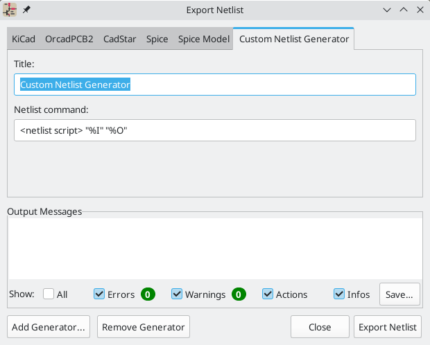
New generators require a name and a command. The name is shown in the tab label, and the command is run whenever the Export Netlist button is clicked.
When the netlist is generated, KiCad creates an intermediate XML file which contains all of the netlist information from the schematic. The generator command is then run in order to transform the intermediate netlist into the desired netlist format.
The netlist command must be set up properly so that the netlist generator script takes the intermediate netlist file as input and outputs the desired netlist file. The exact netlist command will depend on the generator script used. The command format is described below.
Python and XSLT are commonly used tools to create custom netlist generators.
Adding a new BOM generator
KiCad also uses the intermediate netlist file to generate BOMs with the Generate BOM tool.
Additional scripts can be added to the list of BOM generator scripts by clicking the ![]() button. Scripts can be removed by clicking the
button. Scripts can be removed by clicking the ![]() button. The
button. The ![]() button opens the selected script in a text editor.
button opens the selected script in a text editor.
Generator scripts written in Python and XSLT can contain a header comment that describes the generator’s functionality and usage. This header comment is displayed in the BOM dialog as the description for each generator. The header comment must contain the string @package. Everything following that string until the end of the comment is used as the description for the generator.
KiCad automatically fills the command line field when a new generator script is added, but the command line might need to be adjusted by hand depending on the generator script. KiCad attempts to automatically determine the output file extension from the example command line in the generator script’s header.
Generator command line format
The command line for a netlist or BOM exporter defines the command that KiCad will run to generate the selected output file.
For a netlist exporter using xsltproc, an example is:
xsltproc -o %O.net /usr/share/kicad/plugins/netlist_form_pads-pcb.asc.xsl %I
For a BOM exporter using Python, an example is:
/usr/bin/python3 /usr/share/kicad/plugins/bom_csv_grouped_by_value.py "%I" "%O.csv"
It is recommended to surround arguments in the command line with quotes (") in case they contain spaces or other special characters.
|
Some character sequences like %I and %O have a special meaning in the command line, because KiCad replaces them with a filename or path before executing the command.
| Parameter | Replaced with… | Descripción |
|---|---|---|
|
|
Absolute path and filename of the intermediate netlist file, which is the input to the BOM or netlist generator plugin |
|
|
Absolute path and filename of the output BOM or netlist file (without file
extension). An appropriate file extension may need to be specified after the
|
|
|
Base filename of the output BOM or netlist file (without path or file
extension). An appropriate file extension may need to be specified after the
|
|
|
Absolute path of the project directory, without trailing slash. |
Ficheros Netlist Intermedios
When exporting BOM files and netlists, KiCad creates an intermediate netlist file and then runs a separate tool which post-processes the intermediate netlist into the desired netlist or BOM format.
The intermediate netlist uses XML syntax. It contains a large amount of data about the design. Depending on the output (BOM or netlist), different subsets of the complete intermediate netlist file will be included in the final output file.
The structure of the intermediate netlist file is described in detail below.
Because the conversion from intermediate netlist file to output netlist or BOM is a text-to-text transformation, the post-processing filter can be written using Python, XSLT, or any other tool capable of taking XML as input.
XSLT is not recommended for new netlist or BOM exporters; Python or another tool should be used instead. Beginning with KiCad 7, xsltproc is no longer installed with KiCad, although it can be installed separately. Nevertheless, several examples of netlist exporters using XSLT are included below.
|
Estructura del Netlist Intermedio
Este ejemplo muestra una idea del formato del fichero de netlist
<?xml version="1.0" encoding="utf-8"?>
<export version="D">
  <design>
    <source>F:\kicad_aux\netlist_test\netlist_test.sch</source>
    <date>29/08/2010 21:07:51</date>
    <tool>eeschema (2010-08-28 BZR 2458)-unstable</tool>
  </design>
  <components>
    <comp ref="P1">
      <value>CONN_4</value>
      <libsource lib="conn" part="CONN_4"/>
      <sheetpath names="/" tstamps="/"/>
      <tstamps>4C6E2141</tstamps>
    </comp>
    <comp ref="U2">
      <value>74LS74</value>
      <libsource lib="74xx" part="74LS74"/>
      <sheetpath names="/" tstamps="/"/>
      <tstamps>4C6E20BA</tstamps>
    </comp>
    <comp ref="U1">
      <value>74LS04</value>
      <libsource lib="74xx" part="74LS04"/>
      <sheetpath names="/" tstamps="/"/>
      <tstamps>4C6E20A6</tstamps>
    </comp>
    <comp ref="C1">
      <value>CP</value>
      <libsource lib="device" part="CP"/>
      <sheetpath names="/" tstamps="/"/>
      <tstamps>4C6E2094</tstamps>
    <comp ref="R1">
      <value>R</value>
      <libsource lib="device" part="R"/>
      <sheetpath names="/" tstamps="/"/>
      <tstamps>4C6E208A</tstamps>
    </comp>
  </components>
  <libparts/>
  <libraries/>
  <nets>
    <net code="1" name="GND">
      <node ref="U1" pin="7"/>
      <node ref="C1" pin="2"/>
      <node ref="U2" pin="7"/>
      <node ref="P1" pin="4"/>
    </net>
    <net code="2" name="VCC">
      <node ref="R1" pin="1"/>
      <node ref="U1" pin="14"/>
      <node ref="U2" pin="4"/>
      <node ref="U2" pin="1"/>
      <node ref="U2" pin="14"/>
      <node ref="P1" pin="1"/>
    </net>
    <net code="3" name="">
      <node ref="U2" pin="6"/>
    </net>
    <net code="4" name="">
      <node ref="U1" pin="2"/>
      <node ref="U2" pin="3"/>
    </net>
    <net code="5" name="/SIG_OUT">
      <node ref="P1" pin="2"/>
      <node ref="U2" pin="5"/>
      <node ref="U2" pin="2"/>
    </net>
    <net code="6" name="/CLOCK_IN">
      <node ref="R1" pin="2"/>
      <node ref="C1" pin="1"/>
      <node ref="U1" pin="1"/>
      <node ref="P1" pin="3"/>
    </net>
  </nets>
</export>
Estructura del fichero netlist generado
El fichero netlist intermedio cuenta con cinco secciones.
-
La cabecera.
-
La sección de componentes.
-
La sección de bloques de bibliotecas.
-
La sección de bibliotecas.
-
La sección de nodos.
The file content has the delimiter <export>
<export version="D">
...
</export>
La Cabecera
The header has the delimiter <design>
<design>
<source>F:\kicad_aux\netlist_test\netlist_test.sch</source>
<date>21/08/2010 08:12:08</date>
<tool>eeschema (2010-08-09 BZR 2439)-unstable</tool>
</design>
Esta sección puede ser considerada como una sección para comentarios.
La sección de componentes
The component section has the delimiter <components>
<components>
<comp ref="P1">
<value>CONN_4</value>
<libsource lib="conn" part="CONN_4"/>
<sheetpath names="/" tstamps="/"/>
<tstamps>4C6E2141</tstamps>
</comp>
</components>
Esta sección contiene la lista de componentes en el esquema eléctrico. Cada componente es descrito como sigue:
<comp ref="P1">
<value>CONN_4</value>
<libsource lib="conn" part="CONN_4"/>
<sheetpath names="/" tstamps="/"/>
<tstamps>4C6E2141</tstamps>
</comp>| Element name | Element description |
|---|---|
|
name of the lib where this component was found. |
|
component name inside this library. |
|
path of the sheet inside the hierarchy: identify the sheet within the full schematic hierarchy. |
|
timestamp of the component. |
Note about time stamps for components
To identify a component in a netlist and therefore on a board, the timestamp reference is used as unique for each component. However KiCad provides an auxiliary way to identify a component which is the corresponding footprint on the board. This allows the re-annotation of components in a schematic project and does not lose the link between the component and its footprint.
Una marca temporal es un identificador único para cada componente o hoja en el esquema. De todas formas, en jerarquías complejas, la misma hoja es usada mas de una vez, por eso esta hoja contiene componentes con la misma marcha temporal
A given sheet inside a complex hierarchy has an unique identifier: its sheetpath. A given component (inside a complex hierarchy) has a unique identifier: the sheetpath and its timestamp.
La sección Libparts
The libparts section has the delimiter <libparts>, and the content of this section is defined in the schematic libraries.
<libparts>
<libpart lib="device" part="CP">
  <description>Condensateur polarise</description>
  <footprints>
    <fp>CP*</fp>
    <fp>SM*</fp>
  </footprints>
  <fields>
    <field name="Reference">C</field>
    <field name="Valeur">CP</field>
  </fields>
  <pins>
    <pin num="1" name="1" type="passive"/>
    <pin num="2" name="2" type="passive"/>
  </pins>
</libpart>
</libparts>| Element name | Element description |
|---|---|
|
The symbol’s footprint filters. Each footprint filter is in a separate |
|
The symbol’s fields. Each field’s name and value is given in a separate `<field name="fieldname">…</field> tag. |
|
The symbol’s pins. Each pin is given in a separate |
Possible electrical pin types are:
| Pintype | Descripción |
|---|---|
Input |
Usual input pin |
Output |
Usual output |
Bidirectional |
Input or Output |
Tri-state |
Bus input/output |
Pasivo |
Usual ends of passive components |
Unspecified |
Unknown electrical type |
Power input |
Power input of a component |
Power output |
Power output like a regulator output |
Open collector |
Open collector often found in analog comparators |
Open emitter |
Open emitter sometimes found in logic |
Not connected |
Must be left open in schematic |
La sección bibliotecas
The libraries section has the delimiter <libraries>. This section contains the list of schematic libraries used in the project.
<libraries>
  <library logical="device">
    <uri>F:\kicad\share\library\device.lib</uri>
  </library>
  <library logical="conn">
    <uri>F:\kicad\share\library\conn.lib</uri>
  </library>
</libraries>
La sección nodos
The nets section has the delimiter <nets>. This section describes the connectivity of the schematic by listing all nets and the pins connected to each net.
<nets>
  <net code="1" name="GND">
    <node ref="U1" pin="7"/>
    <node ref="C1" pin="2"/>
    <node ref="U2" pin="7"/>
    <node ref="P1" pin="4"/>
  </net>
  <net code="2" name="VCC">
    <node ref="R1" pin="1"/>
    <node ref="U1" pin="14"/>
    <node ref="U2" pin="4"/>
    <node ref="U2" pin="1"/>
    <node ref="U2" pin="14"/>
    <node ref="P1" pin="1"/>
  </net>
</nets>
Un posible nodo contiene lo siguiente.
<net code="1" name="GND">
  <node ref="U1" pin="7"/>
  <node ref="C1" pin="2"/>
  <node ref="U2" pin="7"/>
  <node ref="P1" pin="4"/>
</net>| Element name | Element Description |
|---|---|
|
an internal identifier for this net |
|
the net name |
|
the pin (identified by |
Example netlist exporters
Some example netlist exporters using XSLT are included below.
XSLT itself is an XML language very suitable for XML transformations. The xsltproc program can be used to read the Intermediate XML netlist input file, apply a style-sheet to transform the input, and save the results in an output file. Use of xsltproc requires a style-sheet file using XSLT conventions. The full conversion process is handled by KiCad, after it is configured once to run xsltproc in a specific way.
The document that describes XSL Transformations (XSLT) is available here: http://www.w3.org/TR/xslt
| When writing a new netlist exporter, consider using Python or another tool rather than XSLT. |
PADS netlist example using XSLT
The following example shows how to create an exporter for the PADS netlist format using xlstproc.
The PADS netlist format is comprised of two sections:
-
A list of footprints
-
A list of nets, together with the pads connected to each net.
Below is an XSL style-sheet which converts the intermediate netlist file to the PADS netlist format.
<?xml version="1.0" encoding="ISO-8859-1"?>
<!--XSL style sheet to Eeschema Generic Netlist Format to PADS netlist format
Copyright (C) 2010, SoftPLC Corporation.
GPL v2.
How to use:
https://lists.launchpad.net/kicad-developers/msg05157.html
-->
<!DOCTYPE xsl:stylesheet [
<!ENTITY nl "
"> <!--new line CR, LF -->
]>
<xsl:stylesheet version="1.0" xmlns:xsl="http://www.w3.org/1999/XSL/Transform">
<xsl:output method="text" omit-xml-declaration="yes" indent="no"/>
<xsl:template match="/export">
<xsl:text>*PADS-PCB*&nl;*PART*&nl;</xsl:text>
<xsl:apply-templates select="components/comp"/>
<xsl:text>&nl;*NET*&nl;</xsl:text>
<xsl:apply-templates select="nets/net"/>
<xsl:text>*END*&nl;</xsl:text>
</xsl:template>
<!-- for each component -->
<xsl:template match="comp">
<xsl:text> </xsl:text>
<xsl:value-of select="@ref"/>
<xsl:text> </xsl:text>
<xsl:choose>
<xsl:when test = "footprint != '' ">
<xsl:apply-templates select="footprint"/>
</xsl:when>
<xsl:otherwise>
<xsl:text>unknown</xsl:text>
</xsl:otherwise>
</xsl:choose>
<xsl:text>&nl;</xsl:text>
</xsl:template>
<!-- for each net -->
<xsl:template match="net">
<!-- nets are output only if there is more than one pin in net -->
<xsl:if test="count(node)>1">
<xsl:text>*SIGNAL* </xsl:text>
<xsl:choose>
<xsl:when test = "@name != '' ">
<xsl:value-of select="@name"/>
</xsl:when>
<xsl:otherwise>
<xsl:text>N-</xsl:text>
<xsl:value-of select="@code"/>
</xsl:otherwise>
</xsl:choose>
<xsl:text>&nl;</xsl:text>
<xsl:apply-templates select="node"/>
</xsl:if>
</xsl:template>
<!-- for each node -->
<xsl:template match="node">
<xsl:text> </xsl:text>
<xsl:value-of select="@ref"/>
<xsl:text>.</xsl:text>
<xsl:value-of select="@pin"/>
<xsl:text>&nl;</xsl:text>
</xsl:template>
</xsl:stylesheet>And here is the PADS netlist output file after running xsltproc:
*PADS-PCB*
*PART*
P1 unknown
U2 unknown
U1 unknown
C1 unknown
R1 unknown
*NET*
*SIGNAL* GND
U1.7
C1.2
U2.7
P1.4
*SIGNAL* VCC
R1.1
U1.14
U2.4
U2.1
U2.14
P1.1
*SIGNAL* N-4
U1.2
U2.3
*SIGNAL* /SIG_OUT
P1.2
U2.5
U2.2
*SIGNAL* /CLOCK_IN
R1.2
C1.1
U1.1
P1.3

*END*
La linea de comando para realizar esta conversión es:
kicad\\bin\\xsltproc.exe -o test.net kicad\\bin\\plugins\\netlist_form_pads-pcb.xsl test.tmp
Cadstar netlist example using XSLT
The following example shows how to create an exporter for the Cadstar netlist format using xlstproc.
The Cadstar format is comprised of two sections:
-
The footprint list
-
The Nets list: grouping pads references by nets
Below is an XSL style-sheet which converts the intermediate netlist file to the Cadstar netlist format.
<?xml version="1.0" encoding="ISO-8859-1"?>
<!--XSL style sheet to Eeschema Generic Netlist Format to CADSTAR netlist format
Copyright (C) 2010, Jean-Pierre Charras.
Copyright (C) 2010, SoftPLC Corporation.
GPL v2. -->
<!DOCTYPE xsl:stylesheet [
<!ENTITY nl "
"> <!--new line CR, LF -->
]>
<xsl:stylesheet version="1.0" xmlns:xsl="http://www.w3.org/1999/XSL/Transform">
<xsl:output method="text" omit-xml-declaration="yes" indent="no"/>
<!-- Netlist header -->
<xsl:template match="/export">
<xsl:text>.HEA&nl;</xsl:text>
<xsl:apply-templates select="design/date"/> <!-- Generate line .TIM <time> -->
<xsl:apply-templates select="design/tool"/> <!-- Generate line .APP <eeschema version> -->
<xsl:apply-templates select="components/comp"/> <!-- Generate list of components -->
<xsl:text>&nl;&nl;</xsl:text>
<xsl:apply-templates select="nets/net"/> <!-- Generate list of nets and connections -->
<xsl:text>&nl;.END&nl;</xsl:text>
</xsl:template>
<!-- Generate line .TIM 20/08/2010 10:45:33 -->
<xsl:template match="tool">
<xsl:text>.APP "</xsl:text>
<xsl:apply-templates/>
<xsl:text>"&nl;</xsl:text>
</xsl:template>
<!-- Generate line .APP "eeschema (2010-08-17 BZR 2450)-unstable" -->
<xsl:template match="date">
<xsl:text>.TIM </xsl:text>
<xsl:apply-templates/>
<xsl:text>&nl;</xsl:text>
</xsl:template>
<!-- for each component -->
<xsl:template match="comp">
<xsl:text>.ADD_COM </xsl:text>
<xsl:value-of select="@ref"/>
<xsl:text> </xsl:text>
<xsl:choose>
<xsl:when test = "value != '' ">
<xsl:text>"</xsl:text> <xsl:apply-templates select="value"/> <xsl:text>"</xsl:text>
</xsl:when>
<xsl:otherwise>
<xsl:text>""</xsl:text>
</xsl:otherwise>
</xsl:choose>
<xsl:text>&nl;</xsl:text>
</xsl:template>
<!-- for each net -->
<xsl:template match="net">
<!-- nets are output only if there is more than one pin in net -->
<xsl:if test="count(node)>1">
<xsl:variable name="netname">
<xsl:text>"</xsl:text>
<xsl:choose>
<xsl:when test = "@name != '' ">
<xsl:value-of select="@name"/>
</xsl:when>
<xsl:otherwise>
<xsl:text>N-</xsl:text>
<xsl:value-of select="@code"/>
</xsl:otherwise>
</xsl:choose>
<xsl:text>"&nl;</xsl:text>
</xsl:variable>
<xsl:apply-templates select="node" mode="first"/>
<xsl:value-of select="$netname"/>
<xsl:apply-templates select="node" mode="others"/>
</xsl:if>
</xsl:template>
<xsl:template match="node" mode="others">
<xsl:choose>
<xsl:when test='position()=1'>
</xsl:when>
<xsl:when test='position()=2'>
<xsl:text>.TER </xsl:text>
</xsl:when>
<xsl:otherwise>
<xsl:text> </xsl:text>
</xsl:otherwise>
</xsl:choose>
<xsl:if test="position()>1">
<xsl:value-of select="@ref"/>
<xsl:text>.</xsl:text>
<xsl:value-of select="@pin"/>
<xsl:text>&nl;</xsl:text>
</xsl:if>
</xsl:template>
</xsl:stylesheet>A continuación se muestra el fichero de salida formato Caadstar.
.HEA
.TIM 21/08/2010 08:12:08
.APP "eeschema (2010-08-09 BZR 2439)-unstable"
.ADD_COM P1 "CONN_4"
.ADD_COM U2 "74LS74"
.ADD_COM U1 "74LS04"
.ADD_COM C1 "CP"
.ADD_COM R1 "R"


.ADD_TER U1.7 "GND"
.TER     C1.2
         U2.7
         P1.4
.ADD_TER R1.1 "VCC"
.TER     U1.14
         U2.4
         U2.1
         U2.14
         P1.1
.ADD_TER U1.2 "N-4"
.TER     U2.3
.ADD_TER P1.2 "/SIG_OUT"
.TER     U2.5
         U2.2
.ADD_TER R1.2 "/CLOCK_IN"
.TER     C1.1
         U1.1
         P1.3

.END
OrcadPCB2 netlist example using XSLT
This format has only one section which is the footprint list. Each footprint includes a list of its pads with reference to a net.
Below is an XSL style-sheet which converts the intermediate netlist file to the Orcad netlist format.
<?xml version="1.0" encoding="ISO-8859-1"?>
<!--XSL style sheet to Eeschema Generic Netlist Format to CADSTAR netlist format
Copyright (C) 2010, SoftPLC Corporation.
GPL v2.
How to use:
https://lists.launchpad.net/kicad-developers/msg05157.html
-->
<!DOCTYPE xsl:stylesheet [
<!ENTITY nl "
"> <!--new line CR, LF -->
]>
<xsl:stylesheet version="1.0" xmlns:xsl="http://www.w3.org/1999/XSL/Transform">
<xsl:output method="text" omit-xml-declaration="yes" indent="no"/>
<!--
Netlist header
Creates the entire netlist
(can be seen as equivalent to main function in C
-->
<xsl:template match="/export">
<xsl:text>( { Eeschema Netlist Version 1.1 </xsl:text>
<!-- Generate line .TIM <time> -->
<xsl:apply-templates select="design/date"/>
<!-- Generate line eeschema version ... -->
<xsl:apply-templates select="design/tool"/>
<xsl:text>}&nl;</xsl:text>
<!-- Generate the list of components -->
<xsl:apply-templates select="components/comp"/> <!-- Generate list of components -->
<!-- end of file -->
<xsl:text>)&nl;*&nl;</xsl:text>
</xsl:template>
<!--
Generate id in header like "eeschema (2010-08-17 BZR 2450)-unstable"
-->
<xsl:template match="tool">
<xsl:apply-templates/>
</xsl:template>
<!--
Generate date in header like "20/08/2010 10:45:33"
-->
<xsl:template match="date">
<xsl:apply-templates/>
<xsl:text>&nl;</xsl:text>
</xsl:template>
<!--
This template read each component
(path = /export/components/comp)
creates lines:
( 3EBF7DBD $noname U1 74LS125
... pin list ...
)
and calls "create_pin_list" template to build the pin list
-->
<xsl:template match="comp">
<xsl:text> ( </xsl:text>
<xsl:choose>
<xsl:when test = "tstamp != '' ">
<xsl:apply-templates select="tstamp"/>
</xsl:when>
<xsl:otherwise>
<xsl:text>00000000</xsl:text>
</xsl:otherwise>
</xsl:choose>
<xsl:text> </xsl:text>
<xsl:choose>
<xsl:when test = "footprint != '' ">
<xsl:apply-templates select="footprint"/>
</xsl:when>
<xsl:otherwise>
<xsl:text>$noname</xsl:text>
</xsl:otherwise>
</xsl:choose>
<xsl:text> </xsl:text>
<xsl:value-of select="@ref"/>
<xsl:text> </xsl:text>
<xsl:choose>
<xsl:when test = "value != '' ">
<xsl:apply-templates select="value"/>
</xsl:when>
<xsl:otherwise>
<xsl:text>"~"</xsl:text>
</xsl:otherwise>
</xsl:choose>
<xsl:text>&nl;</xsl:text>
<xsl:call-template name="Search_pin_list" >
<xsl:with-param name="cmplib_id" select="libsource/@part"/>
<xsl:with-param name="cmp_ref" select="@ref"/>
</xsl:call-template>
<xsl:text> )&nl;</xsl:text>
</xsl:template>
<!--
This template search for a given lib component description in list
lib component descriptions are in /export/libparts,
and each description start at ./libpart
We search here for the list of pins of the given component
This template has 2 parameters:
"cmplib_id" (reference in libparts)
"cmp_ref" (schematic reference of the given component)
-->
<xsl:template name="Search_pin_list" >
<xsl:param name="cmplib_id" select="0" />
<xsl:param name="cmp_ref" select="0" />
<xsl:for-each select="/export/libparts/libpart">
<xsl:if test = "@part = $cmplib_id ">
<xsl:apply-templates name="build_pin_list" select="pins/pin">
<xsl:with-param name="cmp_ref" select="$cmp_ref"/>
</xsl:apply-templates>
</xsl:if>
</xsl:for-each>
</xsl:template>
<!--
This template writes the pin list of a component
from the pin list of the library description
The pin list from library description is something like
<pins>
<pin num="1" type="passive"/>
<pin num="2" type="passive"/>
</pins>
Output pin list is ( <pin num> <net name> )
something like
( 1 VCC )
( 2 GND )
-->
<xsl:template name="build_pin_list" match="pin">
<xsl:param name="cmp_ref" select="0" />
<!-- write pin numner and separator -->
<xsl:text> ( </xsl:text>
<xsl:value-of select="@num"/>
<xsl:text> </xsl:text>
<!-- search net name in nets section and write it: -->
<xsl:variable name="pinNum" select="@num" />
<xsl:for-each select="/export/nets/net">
<!-- net name is output only if there is more than one pin in net
else use "?" as net name, so count items in this net
-->
<xsl:variable name="pinCnt" select="count(node)" />
<xsl:apply-templates name="Search_pin_netname" select="node">
<xsl:with-param name="cmp_ref" select="$cmp_ref"/>
<xsl:with-param name="pin_cnt_in_net" select="$pinCnt"/>
<xsl:with-param name="pin_num"> <xsl:value-of select="$pinNum"/>
</xsl:with-param>
</xsl:apply-templates>
</xsl:for-each>
<!-- close line -->
<xsl:text> )&nl;</xsl:text>
</xsl:template>
<!--
This template writes the pin netname of a given pin of a given component
from the nets list
The nets list description is something like
<nets>
<net code="1" name="GND">
<node ref="J1" pin="20"/>
<node ref="C2" pin="2"/>
</net>
<net code="2" name="">
<node ref="U2" pin="11"/>
</net>
</nets>
This template has 2 parameters:
"cmp_ref" (schematic reference of the given component)
"pin_num" (pin number)
-->
<xsl:template name="Search_pin_netname" match="node">
<xsl:param name="cmp_ref" select="0" />
<xsl:param name="pin_num" select="0" />
<xsl:param name="pin_cnt_in_net" select="0" />
<xsl:if test = "@ref = $cmp_ref ">
<xsl:if test = "@pin = $pin_num">
<!-- net name is output only if there is more than one pin in net
else use "?" as net name
-->
<xsl:if test = "$pin_cnt_in_net>1">
<xsl:choose>
<!-- if a net has a name, use it,
else build a name from its net code
-->
<xsl:when test = "../@name != '' ">
<xsl:value-of select="../@name"/>
</xsl:when>
<xsl:otherwise>
<xsl:text>$N-0</xsl:text><xsl:value-of select="../@code"/>
</xsl:otherwise>
</xsl:choose>
</xsl:if>
<xsl:if test = "$pin_cnt_in_net <2">
<xsl:text>?</xsl:text>
</xsl:if>
</xsl:if>
</xsl:if>
</xsl:template>
</xsl:stylesheet>Este es el fichero de salida en formato OrcadPCB2
( { Eeschema Netlist Version 1.1  29/08/2010 21:07:51
eeschema (2010-08-28 BZR 2458)-unstable}
 ( 4C6E2141 $noname P1 CONN_4
  (  1 VCC )
  (  2 /SIG_OUT )
  (  3 /CLOCK_IN )
  (  4 GND )
 )
 ( 4C6E20BA $noname U2 74LS74
  (  1 VCC )
  (  2 /SIG_OUT )
  (  3 N-04 )
  (  4 VCC )
  (  5 /SIG_OUT )
  (  6 ? )
  (  7 GND )
  (  14 VCC )
 )
 ( 4C6E20A6 $noname U1 74LS04
  (  1 /CLOCK_IN )
  (  2 N-04 )
  (  7 GND )
  (  14 VCC )
 )
 ( 4C6E2094 $noname C1 CP
  (  1 /CLOCK_IN )
  (  2 GND )
 )
 ( 4C6E208A $noname R1 R
  (  1 VCC )
  (  2 /CLOCK_IN )
 )
)
*
Actions reference
Below is a list of every available action in the KiCad Schematic Editor: a command that can be assigned to a hotkey.
Schematic Editor
The actions below are available in the Schematic Editor. Hotkeys can be assigned to any of these actions in the Hotkeys section of the preferences.
| Action | Default Hotkey | Descripción |
|---|---|---|
Align to Bottom |
Aligns selected items to the bottom edge of the item under the cursor |
|
Align to Horizontal Center |
Aligns selected items to the horizontal center of the item under the cursor |
|
Align to Vertical Center |
Aligns selected items to the vertical center of the item under the cursor |
|
Align to Left |
Aligns selected items to the left edge of the item under the cursor |
|
Align to Right |
Aligns selected items to the right edge of the item under the cursor |
|
Align to Top |
Aligns selected items to the top edge of the item under the cursor |
|
Align Items to Grid |
||
Add Design Variant… |
Add new design variant to the schematic. |
|
Annotate Schematic… |
Fill in schematic symbol reference designators |
|
Annotate Automatically |
Toggle automatic annotation of new symbols |
|
Assign Footprints… |
Run footprint assignment tool |
|
Clear Net Highlighting |
~ |
Clear any existing net highlighting |
Export Drawing to Clipboard |
Export drawing of current sheet to clipboard |
|
Edit Library Symbol… |
Ctrl+Shift+E |
Open the library symbol in the Symbol Editor |
Edit Sheet Page Number… |
Edit the page number of the current or selected sheet |
|
Bulk Edit Symbol Fields… |
Edit a table of fields from all symbols in the schematic |
|
Bulk Edit Symbol Library Links… |
Edit a table of links between schematic and library symbols |
|
Edit with Symbol Editor |
Ctrl+E |
Open the selected symbol in the Symbol Editor |
Export Netlist… |
Export file containing netlist in one of several formats |
|
Export Symbols… |
Add symbols from schematic to a new or an existing symbol library (does not remove other symbols from this library) |
|
Generate Bill of Materials… |
Generate a bill of materials for the current schematic |
|
Generate Bill of Materials (External)… |
Generate a bill of materials for the current schematic using external generator |
|
Generate Legacy Bill of Materials… |
Generate a bill of materials for the current schematic (Legacy Generator) |
|
Highlight Net |
` |
Highlight net under cursor |
Highlight Nets |
Highlight wires and pins of a net |
|
Import Footprint Assignments… |
Import symbol footprint assignments from .cmp file created by board editor |
|
Import Graphics… |
Ctrl+Shift+F |
Import 2D drawing file |
Increment Annotations From… |
Increment a subset of reference designators starting at a particular symbol |
|
Line Mode for Wires and Buses |
Constrain drawing and dragging to horizontal, vertical, or 45-degree angle motions |
|
Line Mode for Wires and Buses |
Draw and drag at any angle |
|
Line Mode for Wires and Buses |
Shift+Space |
Switch to next angle snapping mode |
Line Mode for Wires and Buses |
Constrain drawing and dragging to horizontal or vertical motions |
|
Mark items excluded from simulation |
Draw 'X’s over items which have been excluded from simulation |
|
Next Net Item |
Tab |
Select next item on the current net |
Next Symbol Unit |
Open the next unit of the symbol |
|
Previous Net Item |
Shift+Tab |
Select previous item on the current net |
Previous Symbol Unit |
Open the previous unit of the symbol |
|
Remap Legacy Library Symbols… |
Remap library symbol references in legacy schematics to the symbol library table |
|
Remove Design Variant… |
Remove an existing design variant from the schematic. |
|
Rescue Symbols… |
Find old symbols in project and rename/rescue them |
|
Save Current Sheet Copy As… |
Save a copy of the current sheet to another location or name |
|
Schematic Setup… |
Edit schematic setup including annotation styles and electrical rules |
|
Select on PCB |
Select corresponding items in PCB editor |
|
Do not Populate |
Set the do not populate attribute |
|
Exclude from Bill of Materials |
Set the exclude from bill of materials attribute |
|
Exclude from Board |
Set the exclude from board attribute |
|
Exclude from Simulation |
Set the exclude from simulation attribute |
|
Show Directive Labels |
||
Show ERC Errors |
Show markers for electrical rules checker errors |
|
Show ERC Exclusions |
Show markers for excluded electrical rules checker violations |
|
Show ERC Warnings |
Show markers for electrical rules checker warnings |
|
Show Hidden Fields |
||
Show Hidden Pins |
||
Net Navigator |
Show/hide the net navigator |
|
Show OP Currents |
Show operating point current data from simulation |
|
Show OP Voltages |
Show operating point voltage data from simulation |
|
Switch to PCB Editor |
Open PCB in board editor |
|
Simulator |
Show simulation window for running SPICE or IBIS simulations. |
|
Show Pin Alternate Icons |
Show indicator icons for pins with alternate modes |
|
Hierarchy Navigator |
Ctrl+H |
Show/hide the schematic sheet hierarchy navigator |
Symbol Checker |
Show the symbol checker window |
|
Compare Symbol with Library |
Show differences between schematic symbol and its library equivalent |
|
Electrical Rules Checker |
Show the electrical rules checker window |
|
Show Bus Syntax Help |
||
Decrement Primary |
Decrement the primary field of the selected item(s) |
|
Decrement Secondary |
Decrement the secondary field of the selected item(s) |
|
Increment |
Increment the selected item(s) |
|
Increment Primary |
Increment the primary field of the selected item(s) |
|
Increment Secondary |
Increment the secondary field of the selected item(s) |
|
Autoplace All Sheet Pins |
Imports and auto places all sheet pins |
|
Close Outline |
Close the in-progress outline |
|
Delete Last Point |
Delete the last point added to the current item |
|
Draw Arcs |
||
Draw Bezier Curve |
||
Draw Circles |
||
Draw Rectangles |
||
Draw Rule Areas |
||
Draw Hierarchical Sheets |
S |
|
Draw Sheet from Design Block |
Copy design block into project as a sheet on current sheet |
|
Draw Sheet from File |
Copy sheet into project and draw on current sheet |
|
Draw Tables |
||
Draw Text Boxes |
||
Import Sheet… |
Import sheet into project |
|
Place Wire to Bus Entries |
Z |
|
Place Directive Labels |
||
Place Design Block |
Shift+B |
Add selected design block to current sheet |
Place Global Labels |
Ctrl+L |
|
Place Hierarchical Labels |
H |
|
Place Images |
||
Place Junctions |
J |
|
Place Net Labels |
L |
|
Place Linked Design Block |
Place design block linked to selected group |
|
Place Next Symbol Unit |
Place the next unit of the current symbol that is missing from the schematic |
|
Place No Connect Flags |
Q |
|
Place Power Symbols |
P |
|
Draw Text |
T |
|
Place Pins from Sheet |
Add sheet pins from existing hierarchical labels found on that sheet |
|
Place Symbols |
A |
|
Save to Linked Design Block |
Save selected group to linked design block |
|
Sync All Sheet Pins… |
Synchronize all sheet pins and hierarchical labels |
|
Sync Selected Sheet Pins… |
Synchronize selected sheet pins and hierarchical labels |
|
Draw Buses |
B |
|
Draw Lines |
I |
|
Draw Wires |
W |
|
Switch Segment Posture |
/ |
Switches posture of the current segment. |
Undo Last Segment |
Back |
Walks the current line back one segment. |
Unfold from Bus |
C |
Break a wire out of a bus |
Assign Netclass… |
Assign a netclass to nets matching a pattern |
|
Autoplace Fields |
O |
Runs the automatic placement algorithm on the symbol’s (or sheet’s) fields |
Break |
Divide into connected segments |
|
Change Symbol… |
Assign a different symbol from the library |
|
Change Symbols… |
Assign different symbols from the library |
|
Cleanup Sheet Pins |
Delete unreferenced sheet pins |
|
Convert Stacked Pins |
Convert multiple pins at the same location to a single pin with stacked notation |
|
Edit Footprint… |
F |
|
Edit Reference Designator… |
U |
|
Edit Text & Graphics Properties… |
Edit text and graphics properties globally across schematic |
|
Edit Value… |
V |
|
Explode Stacked Pin |
Convert a pin with stacked notation to multiple individual pins |
|
Find in Net Navigator |
Locate the selected net in the net navigator |
|
Mirror Horizontally |
X |
Flips selected item(s) from left to right |
Mirror Vertically |
Y |
Flips selected item(s) from top to bottom |
Pin Table… |
Displays pin table for bulk editing of pins |
|
Properties… |
E |
|
Repeat Last Item |
Ins |
Duplicates the last drawn item |
Rotate Counterclockwise |
R |
|
Rotate Clockwise |
Shift+R |
|
Slice |
Divide into unconnected segments |
|
Swap |
Alt+S |
Swap positions of selected items |
Swap Pin Labels |
Swap the labels attached to selected pins |
|
Swap Pins |
Swap the selected symbol pins' positions |
|
Swap Unit Labels |
Swap labels between selected units |
|
Symbol Properties… |
||
Change to Directive Label |
Change existing item to a directive label |
|
Change to Global Label |
Change existing item to a global label |
|
Change to Hierarchical Label |
Change existing item to a hierarchical label |
|
Change to Label |
Change existing item to a label |
|
Change to Text |
Change existing item to a text comment |
|
Change to Text Box |
Change existing item to a text box |
|
Cycle Body Style |
Switch between De Morgan (or other) representations |
|
Update Symbol… |
Update symbol to include any changes from the library |
|
Update Symbols from Library… |
Update symbols to include any changes from the library |
|
Drag |
G |
Move items while keeping their connections |
Move |
M |
|
Select/Expand Connection |
Ctrl+4 |
Selects a connection or expands an existing selection to pins, symbols, or entire connections |
Select Node |
Alt+3 |
Select a connection item under the cursor |
Navigate Back |
Alt+Left |
Move backward in sheet navigation history |
Change Sheet |
Change to provided sheet’s contents in the schematic editor |
|
Enter Sheet |
Display the selected sheet’s contents in the schematic editor |
|
Navigate Forward |
Alt+Right |
Move forward in sheet navigation history |
Leave Sheet |
Alt+Back |
Display the parent sheet in the schematic editor |
Next Sheet |
PgDn |
Move to next sheet by number |
Previous Sheet |
PgUp |
Move to previous sheet by number |
Navigate Up |
Alt+Up |
Navigate up one sheet in the hierarchy |
Push Pin Length |
Copy pin length to other pins in symbol |
|
Push Pin Name Size |
Copy pin name size to other pins in symbol |
|
Push Pin Number Size |
Copy pin number size to other pins in symbol |
|
Create Corner |
||
Remove Corner |
||
Remote Symbols |
Show/hide the remote symbol panel |
|
Delete Design Block |
Remove the selected design block from its library |
|
Properties… |
Edit properties of design block |
|
Save Selection as Design Block… |
Create a new design block from the current selection |
|
Save Current Sheet as Design Block… |
Create a new design block from the current sheet |
|
Design Blocks |
Show/hide design blocks library |
|
Update Design Block from Selection |
Set design block schematic to current selection |
|
Update Design Block from Current Sheet |
Set design block schematic to current sheet |
|
User-defined Signals… |
Add, edit or delete user-defined simulation signals |
|
New Analysis Tab… |
Ctrl+N |
Create a new tab containing a simulation analysis |
Open Workbook… |
Ctrl+O |
Open a saved set of analysis tabs and settings |
Probe Schematic… |
Shift+P |
Add a simulator probe |
Run Simulation |
R |
|
Save Workbook |
Ctrl+S |
Save the current set of analysis tabs and settings |
Save Workbook As… |
Ctrl+Shift+S |
Save the current set of analysis tabs and settings to another location |
Show SPICE Netlist |
||
Edit Analysis Tab… |
Edit the current analysis tab’s SPICE command and plot setup |
|
Stop Simulation |
||
Add Tuned Value… |
Shift+T |
Select a value to be tuned |
Export Current Plot as CSV… |
||
Export Current Plot as PNG… |
||
Export Current Plot to Schematic |
||
Export Current Plot to Clipboard |
||
Dark Mode Plots |
Draw plots with a black background |
|
Dotted Current/Phase |
Draw secondary signal trace (current or phase) with a dotted line |
|
Show Legend |
||
Show Simulation Console Panel |
||
Show Simulation Side Panel |
||
Draw Lines |
Draw connected graphic lines |
|
Draw Polygons |
||
Draw Text Boxes |
||
Move Symbol Anchor |
||
Draw Pins |
P |
|
Draw Text |
||
Add Symbol to Schematic |
Add the current symbol to the schematic |
|
Copy |
||
Cut |
||
Delete Symbol |
Remove the selected symbol from its library |
|
Derive from Existing Symbol… |
Create a new symbol, derived from an existing symbol |
|
Duplicate Symbol |
||
Edit Symbol |
Show selected symbol on editor canvas |
|
Export… |
Export a symbol to a new library file |
|
Export Symbol as SVG… |
Create SVG file from the current symbol |
|
Export View as PNG… |
Create PNG file from the current view |
|
Flatten Symbol |
Remove inheritance from symbol |
|
Import Symbol… |
Import a symbol to the current library |
|
New Symbol… |
Ctrl+N |
Create a new symbol in an existing library |
Display next symbol |
||
Paste Symbol |
||
Display previous symbol |
||
Rename Symbol… |
||
Save Library As… |
Ctrl+Shift+S |
Save the current library to a new file |
Save As… |
Save the current symbol to a different library or name |
|
Save Copy As… |
Save a copy of the current symbol to a different library or name |
|
Show Pin Electrical Types |
Annotate pins with their electrical types |
|
Show Hidden Fields |
||
Show Hidden Pins |
||
Bulk Edit Symbol Fields… |
Edit a table of fields from all symbols in the library |
|
Show Pin Numbers |
Annotate pins with their numbers |
|
Bulk Edit Related Symbol Fields… |
Edit a table of fields from all symbols related to the selected symbol |
|
Synchronized Pins Mode |
Synchronized Pins Mode When enabled propagates all changes (except pin numbers) to other units. Enabled by default for multiunit parts with interchangeable units. |
|
Update Symbol Fields… |
Update symbol to match changes made in parent symbol |
Common
The actions below are available across KiCad, including in the Schematic Editor. Hotkeys can be assigned to any of these actions in the Hotkeys section of the preferences.
| Action | Default Hotkey | Descripción |
|---|---|---|
Close |
Ctrl+W |
|
Quit |
Ctrl+Q |
|
Refresh Plugins |
Reload all python plugins and refresh plugin menus |
|
Exclude Marker |
Mark current violation in Checker window as an exclusion |
|
Next Marker |
||
Previous Marker |
||
Add Library… |
Add an existing library folder |
|
Center Justify |
Center-justify fields and text items |
|
Pan to Center Selected Objects |
||
Collapse All |
||
45 Degree Crosshairs |
Display full-window crosshairs aligned at 45 and 135 degrees |
|
Click |
Return |
Performs left mouse button click |
Double-click |
End |
Performs left mouse button double-click |
Cursor Down |
Down |
|
Cursor Down Fast |
Ctrl+Down |
|
Full-Window Crosshairs |
Display full-window crosshairs aligned at 0 and 90 degrees |
|
Cursor Left |
Left |
|
Cursor Left Fast |
Ctrl+Left |
|
Cursor Right |
Right |
|
Cursor Right Fast |
Ctrl+Right |
|
Small crosshairs |
Use small crosshairs aligned at 0 and 90 degrees |
|
Cursor Up |
Up |
|
Cursor Up Fast |
Ctrl+Up |
|
Grid Origin… |
Set the grid origin point |
|
Edit Grids… |
Edit grid definitions |
|
Expand All |
||
Switch to Fast Grid 1 |
Alt+1 |
|
Switch to Fast Grid 2 |
Alt+2 |
|
Cycle Fast Grid |
Alt+4 |
|
Switch to Next Grid |
N |
|
Switch to Previous Grid |
Shift+N |
|
Reset Grid Origin |
||
Grid Origin |
Place the grid origin point |
|
Hide Library Tree |
||
Inactive Layer View Mode |
Toggle inactive layers between normal and dimmed |
|
Inactive Layer View Mode (3-state) |
H |
Cycle inactive layers between normal, dimmed, and hidden |
Inches |
||
Left Justify |
Left-justify fields and text items |
|
Focus Library Tree Search Field |
Ctrl+L |
|
Snap to Objects on the Active Layer Only |
Enables snapping to objects on the active layer only |
|
Snap to Objects on All Layers |
Enables snapping to objects on all visible layers |
|
Toggle Snapping Between Active and All Layers |
Shift+S |
Toggles between snapping on all visible layers and only the active area |
Millimeters |
||
Mils |
||
New… |
Ctrl+N |
Create a new document in the editor |
New Library… |
Create a new library folder |
|
Open… |
Ctrl+O |
Open existing document |
Open in file explorer… |
Open a library file with system file explorer |
|
Edit in a Text Editor… |
Open a library file with a text editor |
|
Page Settings… |
Settings for paper size and title block info |
|
Pan Down |
Shift+Down |
|
Pan Left |
Shift+Left |
|
Pan Right |
Shift+Right |
|
Pan Up |
Shift+Up |
|
Pin Library |
Keep the library at the top of the list |
|
Plot… |
||
Print… |
Ctrl+P |
|
Quit |
Close the current editor |
|
Redo Last Zoom |
Return zoom to level prior to last zoom undo |
|
Reset Local Coordinates |
Space |
|
Revert |
Throw away changes |
|
Right Justify |
Right-justify fields and text items |
|
Save |
Ctrl+S |
Save changes |
Save All |
Save all changes |
|
Save As… |
Ctrl+Shift+S |
Save current document to another location |
Save a Copy… |
Save a copy of the current document to another location |
|
Select Columns… |
||
3D Viewer |
Alt+3 |
Show 3D viewer window |
Calculator Tools |
Run component calculations, track width calculations, etc. |
|
Show Context Menu |
Perform the right-mouse-button action |
|
Show Datasheet |
D |
Open the datasheet in a browser |
Footprint Library Browser |
||
Footprint Editor |
Create, delete and edit board footprints |
|
Library Tree |
||
Switch to Project Manager |
Show project window |
|
Propiedades |
Show/hide the properties manager |
|
Symbol Library Browser |
||
Symbol Editor |
Create, delete and edit schematic symbols |
|
Draw Bounding Boxes |
||
Always Show Crosshairs |
Display crosshairs even when not drawing objects |
|
Show Grid |
Display background grid in the edit window |
|
Grid Overrides |
Ctrl+Shift+G |
Enables item-specific grids that override the current grid |
Polar Coordinates |
Switch between polar and cartesian coordinate systems |
|
Switch units |
Ctrl+U |
Switch between imperial and metric units |
Undo Last Zoom |
Return zoom to level prior to last zoom action |
|
Unpin Library |
No longer keep the library at the top of the list |
|
Update PCB from Schematic… |
F8 |
Update PCB with changes made to schematic |
Update Schematic from PCB… |
Update schematic with changes made to PCB |
|
Center on Cursor |
F4 |
|
Zoom to All Objects |
Ctrl+Home |
Zoom to all objects on screen |
Zoom to Fit |
Home |
Zoom to worksheet area if exists or edited object |
Zoom to Selected Objects |
Zoom to items currently selected |
|
Zoom In at Cursor |
F1 |
|
Zoom In |
||
Zoom In Horizontally |
Zoom in horizontally the plot area |
|
Zoom In Vertically |
Zoom in vertically the plot area |
|
Zoom Out at Cursor |
F2 |
|
Zoom Out |
||
Zoom Out Horizontally |
Zoom out horizontally the plot area |
|
Zoom Out Vertically |
Zoom out vertically the plot area |
|
Refresh |
F5 |
|
Zoom to Selection Area |
Ctrl+F5 |
Zoom to an area selection created by a mouse drag |
Embedded Files |
Manage embedded files |
|
Extract File |
Extract an embedded file |
|
Remove File |
Remove an embedded file |
|
Add Items |
Add items to group |
|
Cancel |
Cancel current tool |
|
Copy |
Ctrl+C |
Copy selected item(s) to clipboard |
Copy as Text |
Ctrl+Shift+C |
Copy selected item(s) to clipboard as text |
Cut |
Ctrl+X |
Cut selected item(s) to clipboard |
Cycle Arc Editing Mode |
Ctrl+Space |
Switch to a different method of editing arcs |
Delete |
Del |
Delete selected item(s) |
Interactive Delete Tool |
Delete clicked items |
|
Duplicate |
Ctrl+D |
Duplicates the selected item(s) |
Find |
Ctrl+F |
|
Find and Replace |
Ctrl+Alt+F |
|
Find Next |
F3 |
|
Find Next Marker |
Ctrl+Shift+F3 |
|
Find Previous |
Shift+F3 |
|
Finish |
End |
Finish current tool |
Group Items |
Group the selected items so that they are treated as a single item |
|
Enter Group |
Enter the group to edit items |
|
Leave Group |
Leave the current group |
|
Measure Tool |
Ctrl+Shift+M |
Interactively measure distance between points |
Paste |
Ctrl+V |
Paste item(s) from clipboard |
Paste Special… |
Ctrl+Shift+V |
Paste item(s) from clipboard with options |
Redo |
Ctrl+Y |
|
Remove Items |
Remove items from group |
|
Replace All |
||
Replace and Find Next |
||
Search |
Ctrl+G |
Show/hide the search panel |
Select All |
Ctrl+A |
Select all items on screen |
Lasso |
Set selection mode to use polygon lasso |
|
Rectangle |
Set selection mode to use rectangle |
|
Undo |
Ctrl+Z |
|
Ungroup Items |
Ungroup any selected groups |
|
Unselect All |
Ctrl+Shift+A |
Unselect all items on screen |
Select Row(s) |
Select complete row(s) containing the current selected cell(s) |
|
Select Column(s) |
Select complete column(s) containing the current selected cell(s) |
|
Select Table |
Select parent table of selected cell(s) |
|
Select item(s) |
||
About KiCad |
||
Configure Paths… |
Edit path configuration environment variables |
|
Donate |
Open "Donate to KiCad" in a web browser |
|
Get Involved |
Open "Contribute to KiCad" in a web browser |
|
Getting Started with KiCad |
Open “Getting Started in KiCad” guide for beginners |
|
Help |
Open product documentation in a web browser |
|
List Hotkeys… |
Ctrl+F1 |
Displays current hotkeys table and corresponding commands |
Preferences… |
Ctrl+, |
Show preferences for all open tools |
Report Bug |
Report a problem with KiCad |
|
Manage Design Block Libraries… |
Edit the global and project design block library lists |
|
Manage Footprint Libraries… |
Edit the global and project footprint library lists |
|
Manage Symbol Libraries… |
Edit the global and project symbol library lists |
|
Add Column After |
Insert a new table column after the selected cell(s) |
|
Add Column Before |
Insert a new table column before the selected cell(s) |
|
Add Row Above |
Insert a new table row above the selected cell(s) |
|
Add Row Below |
Insert a new table row below the selected cell(s) |
|
Delete Column(s) |
Delete columns containing the currently selected cell(s) |
|
Delete Row(s) |
Delete rows containing the currently selected cell(s) |
|
Merge Cells |
Turn selected table cells into a single cell |
|
Unmerge Cells |
Turn merged table cells back into separate cells. |