封装和封装库
KiCad organizes footprints into footprint libraries, which hold collections of footprints. Each footprint in a board is uniquely identified by a full name that is composed of a library nickname and a footprint name. For example, the identifier Capacitor_SMD:C_0603_1608Metric refers to the C_0603_1608Metric footprint in the Capacitor_SMD library.
管理封装库
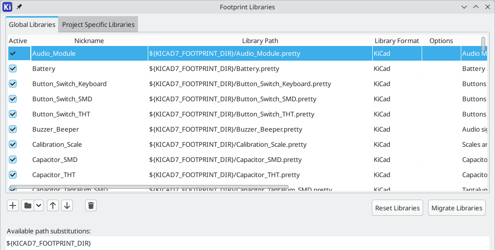
KiCad 使用一个封装库表,将所有支持的库类型的封装库映射到库的昵称(Nickname)。KiCad 使用一个全局封装库表,以及一个针对每个工程的表。要编辑任何一个封装库表,请使用 偏好设置→ 管理封装库…。
全局封装库表包含了始终可以使用的库列表,无论当前加载的工程是什么。该表保存在 KiCad 配置文件夹中的 fp-lib-table 文件中。该文件夹的位置 取决于正在使用的操作系统。
工程专用的封装库表包含了专门为当前加载的工程提供的库的列表。如果有任何工程专用的封装库,该表将保存在工程文件夹中的 fp-lib-table 文件中。
KiCad’s footprint library management system allows directly using many types of footprint libraries, including formats that are native to other non-KiCad EDA tools:
-
KiCad
.prettyfootprint libraries (folders with.prettyextension, containing.kicad_modfiles) -
KiCad Legacy footprint libraries (
.modfiles) -
Altium Designer (
.PcbLibor.IntLibfiles) -
CADSTAR PCB Archive (
.cpafiles) -
Eagle footprint libraries (
.lbrfiles) -
EasyEDA / JLCEDA Standard Edition (
.jsonor.zipfiles) -
EasyEDA / JLCEDA Professional Edition (
.elibz,.epro, or.zipfiles) -
GEDA libraries (folders containing
.fpfiles)
Non-KiCad footprint libraries, including KiCad Legacy footprint libraries, can be migrated to KiCad .pretty format using the Migrate Libraries button (see the migrating libraries section).
KiCad only supports writing to KiCad’s native .pretty format footprint libraries (and the .kicad_mod footprint files within them). All other footprint library formats are read-only. To modify a non-KiCad format footprint library, you must first convert it to KiCad format.
|
初始配置
The first time the PCB Editor (or any other KiCad tool that uses footprints) runs and the global footprint table file fp-lib-table is not found, KiCad will guide the user through setting up a new footprint library table. This process is described above. You can re-run this process at any time by clicking the Reset Libraries.
| Resetting your footprint library table will permanently change your footprint library table on disk. |
管理表的条目
封装库只有在被添加到全局或工程专用的封装库表中时才能被使用。
通过点击 ![]() 按钮并选择一个库或点击
按钮并选择一个库或点击 ![]() 按钮并输入库文件的路径来添加一个库。选定的库将被添加到当前打开的库表中(全局或工程专用)。可以通过选择所需的库条目并点击
按钮并输入库文件的路径来添加一个库。选定的库将被添加到当前打开的库表中(全局或工程专用)。可以通过选择所需的库条目并点击 ![]() 按钮来删除库。
按钮来删除库。
点击 ![]() 和
和![]() 按钮在库表中上下移动所选库。这并不影响在 "封装库浏览器"、"封装编辑器 "或 "添加封装工具 "中显示库的顺序。
按钮在库表中上下移动所选库。这并不影响在 "封装库浏览器"、"封装编辑器 "或 "添加封装工具 "中显示库的顺序。
通过取消选中第一列中的 活动 复选框,可以使库处于非活动状态。 非活动库仍在库表中,但不会出现在任何库浏览器中,也不会从磁盘加载,这样可以减少加载时间。
点击范围内的第一个库,然后 Shift 点击范围内的最后一个库,可以选择一系列库。
每个库必须有一个独特的昵称:在同一个表中不允许有重复的库昵称。然而,昵称可以在全局和工程库表中重复。工程表中的库比全局表中的同名库更有优先权。
库的昵称不一定要与库的文件名或路径有关。冒号字符 (:) 不能用于库昵称或封装名称,因为它被用作昵称和封装之间的分隔符。
Each library entry must have a valid path. Paths can be defined as absolute, relative, or by path variable substitution.
The appropriate library format must be selected in order for the library to be properly read. The supported formats are listed above. Only KiCad format libraries (.pretty folders containing .kicad_mod files) can be saved. Other footprint library formats are read-only and must be converted to KiCad format before you can modify them.
有一个可选的描述字段,用于添加库条目的描述。选项字段目前不使用,所以添加选项在加载库时不会有任何影响。
Path Variable Substitution
The footprint library tables support path variable substitution, which allows you to define path variables containing custom paths to where your libraries are stored. PATH variable substitution is supported by using the syntax ${PATH_VAR_NAME} in the footprint library path.
By default, KiCad defines several path variables which are described in the project manager documentation. Path variables can be configured in the Preferences → Configure Paths… dialog.
Using path variables in the footprint library tables allows libraries to be relocated without breaking the footprint library tables, so long as the path variables are updated when the library location changes.
KiCad will automatically resolve versioned path variables from
older versions of KiCad to the value of the corresponding variable from
the current KiCad version, as long as the old variable is not explicitly
defined itself. For example, ${KICAD8_FOOTPRINT_DIR} will
automatically resolve to the value of ${KICAD9_FOOTPRINT_DIR} if there
is no KICAD8_FOOTPRINT_DIR variable defined.
|
${KIPRJMOD} is a special path variable that always expands to the absolute path of the current project directory. ${KIPRJMOD} allows libraries to be stored in the project folder without having to use an absolute path in the project library table. This makes it possible to relocate projects without breaking their project library tables.
使用 GitHub 插件
| KiCad 在 6.0 版本中取消了对 GitHub 库插件的支持。 |
Migrating footprint libraries to KiCad format
Non-KiCad format libraries, including legacy libraries (.mod files), are read-only. They need to be converted to KiCad format (.kicad_mod files in a .pretty folder) before you can save changes to them.
| As with most KiCad files, newer versions of KiCad can open older-format library files, but older versions of KiCad cannot read files once they have been saved by a newer version of KiCad. |
Libraries in other formats can be converted to KiCad libraries by selecting them in the footprint library table and clicking the Migrate Libraries button. Multiple libraries can be selected and migrated at once by Ctrl-clicking or shift-clicking.
Libraries can also be converted one at a time by opening them in the Footprint Editor and saving them as a new library.
创建和编辑封装
A footprint is the physical interface between a component package and a circuit board. Footprints can contain:
-
Pads, which define how the component will be physically assembled onto the footprint. When a footprint is added to a board, tracks are routed to pads, and pads provide a magnetic snapping point for the router to connect the pad to a track. Pad shapes and layers are fully customizable, and pads can have plated holes, unplated holes, or no hole.
-
Graphic shapes and text for technical or aesthetic purposes. Graphics can be placed on physical layers (e.g. silkscreen or soldermask) or nonphysical layers. Graphic shapes can also be placed on copper layers, in which case they can make electrical connections.
-
3D models for mechanical CAD and visualization. 3D models are normally external files that footprints can link to, but they can optionally be embedded in footprints.
-
Metadata associated with the footprint.
Footprints in KiCad are organized into footprint libraries, which contain zero or more footprints. Generally footprints are logically grouped by footprint category, function, and/or manufacturer. Each library is a folder (usually ending in .pretty) containing a .kicad_mod file for each footprint in the library.
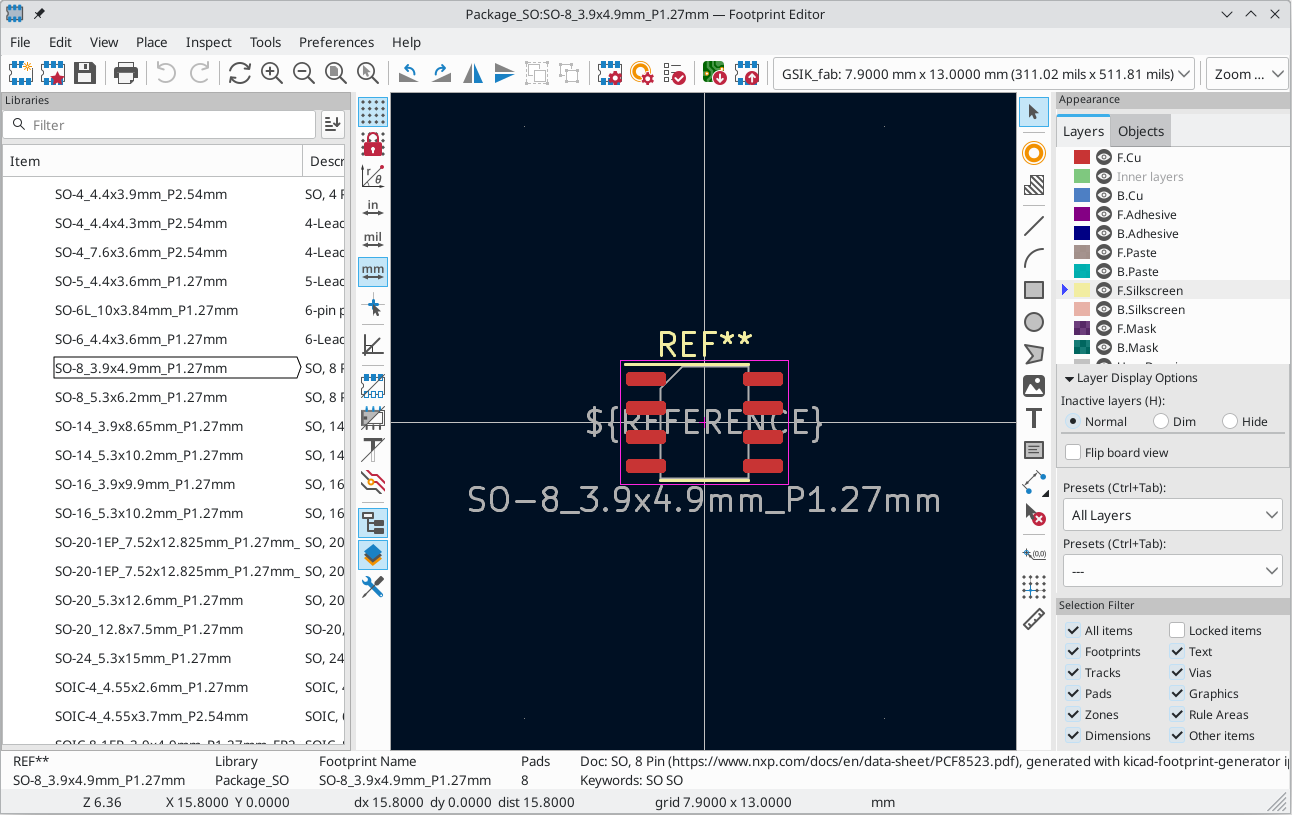
Footprint editor overview
KiCad provides a footprint editing tool that allows you to create footprint libraries; add, edit, delete, or transfer footprints between libraries; export footprints to files; and import footprints from files. The Footprint Editor can be launched from the KiCad Project Manager or from the Board Editor (Tools → Footprint Editor). You can also open the Footprint Editor from the a footprint in the board; in this way you can edit either the library copy or the board copy of that footprint in the editor.
| Editing the library version of a footprint will not affect any copies of that footprint that have been added to a board until the board copy is updated from the library. Conversely, editing the board version of a footprint will not affect the library version of a footprint or any other copies of that footprint in a board. |
The Footprint Editor main window is shown below. It has three toolbars for quick access to common features and a footprint viewing/editing canvas. Not all commands are available on the toolbars, but all commands are available in the menus.
In addition to the toolbars, there are collapsible panels for the footprint tree and Properties Manager (not shown) on the left, and the appearance panel and selection filter on the right. The bottom of the window contains a message panel that shows details about the selected object.
Top toolbar
The main toolbar is at the top of the main window. It has buttons for the undo/redo commands, zoom commands, footprint/pad properties dialogs, and layer/grid management controls.
|
Create a new footprint in the selected library. |
|
Create a new footprint in the selected library using a footprint wizard. |
|
Save the currently selected footprint. |
|
Print the currently selected footprint. |
|
Undo last edit. |
|
Redo last undo. |
|
Refresh display. |
|
Zoom in. |
|
Zoom out. |
|
Zoom to fit footprint in display. |
|
Zoom to fit selection. |
|
Rotate selected item(s) counter-clockwise. |
|
Rotate selected item(s) clockwise. |
|
Mirror selected item(s) horizontally. |
|
Mirror selected item(s) vertically. |
|
Add the selected item(s) to a group. |
|
Remove the selected item(s) from a group. |
|
Edit the current footprint’s properties. |
|
Edit the selected pad’s properties. |
|
Open the current footprint’s datasheet. |
|
Run the footprint checker to test the current footprint for design errors. |
|
Edit a footprint in the current board in the footprint editor. |
|
Insert current footprint into the board. |
左侧工具栏显示控件
The left toolbar provides options to change the display of items in the Footprint Editor.
|
Turn grid display on/off. Note: by default, hiding the grid does not disable grid snapping. This behavior can be changed in the Display Options section of Preferences. |
|
Turn item-specific grid overrides on/off. |
|
Switch between polar and Cartesian coordinate display in the status bar. |
|
Display/entry of coordinates and dimensions in inches, mils, or millimeters. |
|
Switch between full-screen and small editing cursor (crosshairs). |
|
Switch between free angle and 45 degree mode for placement of new tracks, zones, graphical shapes, dimensions, and other objects. You can also toggle between free angle and 45 degree mode using Shift+Space. |
|
Switch display of pads between filled and outline mode. |
|
Switch display of graphic items between filled and outline mode. |
|
Switch display of text between filled and outline mode. |
|
Switch the non-active layer display mode between Normal and Dim. Note: this button will be highlighted when the non-active layer display mode is either Dim or Hide. In both cases, pressing the button will change the layer display mode to Normal. The Hide mode can only be accessed via the controls in the Appearance Panel or via the hotkey Ctrl+H. |
|
Toggle display of library and footprint tree. |
|
Show or hide the Appearance and Selection Filter panels on the right side of the editor. |
|
Show or hide the Properties Manager panel on the left side of the editor. |
Right toolbar tools
Placement and drawing tools are located in the right toolbar.
|
Selection tool (the default tool). |
|
Add pad: click on the board to place a pad. |
|
Add rule area: Rule areas, formerly known as keepouts, can restrict the placement of items and the filling of zones and can also define named areas to apply specific custom design rules to. |
|
Note: Lines are graphical objects and are not the same as tracks placed with the Route Tracks tool. Graphical objects cannot be assigned to a net. |
|
Draw arcs: pick the center point of the arc, then the start and end points. By right clicking this button, you can change the arc editing mode between a mode that maintains the existing arc center and a mode that maintains the arc radius. |
|
Draw rectangles. Rectangles can be filled or outlines. |
|
Draw circles. Circles can be filled or outlines. |
|
Draw graphical polygons. Polygons can be filled or outlined. Note: Filled graphical polygons are not the same as filled zones: graphical polygons cannot be assigned to a net and will not keep clearance from other items. |
|
Draw bezier curves: draw a bezier curve. Each curve is defined by its start and end points and two control points. Subsequent curves start as tangent to the previous one. Use Backspace to cancel the previous point. |
|
Add bitmap image for reference. Reference images are not included in fabrication outputs. |
|
|
|
|
|
|
|
Add dimensions. Dimension types are described in more detail below. |
|
Deletion tool: click objects to delete them. |
|
Anchor tool. Left-click to set the anchor position (origin) of the footprint. |
|
|
|
Interactively measure the distance between two points. |
Browsing, modifying, and saving footprints
The ![]() button displays or hides the list of available libraries, which allows you to select an active library. When a new footprint is created, it will be placed in the active library.
button displays or hides the list of available libraries, which allows you to select an active library. When a new footprint is created, it will be placed in the active library.
Clicking on a footprint name opens that footprint in the editor, and hovering the cursor over the name of a footprint displays a preview of the footprint.
After modification, a footprint can be saved in the current library or a different library. To save the modified footprint in the current library, click the ![]() button.
button.
To save the footprint changes to a new footprint, click File → Save As…. The footprint can be saved in the current library or a different library, and a new name can be set for the footprint.
To create a new file containing only the current footprint, click File → Export → Footprint…. This file will be a standard footprint library which will contain only one footprint.
The editor can also open footprints from the board. To edit a footprint from the board, right click a footprint in the Board Editor and select Open in Footprint Editor (Ctrl+E). Alternatively, you can open a board footprint by pressing the ![]() button in the Footprint Editor top toolbar and selecting the desired footprint.
button in the Footprint Editor top toolbar and selecting the desired footprint.
Editing and saving the board copy of a footprint will only update that footprint in the board; it will not update other copies of that footprint in the board, and it will not change the original library copy of the footprint. When you open the board copy of a footprint, the Footprint Editor displays an info bar that warns you the library copy will not be modified. You can click the link in this info bar to open the library version of the footprint instead, or press Ctrl+Shift+E.
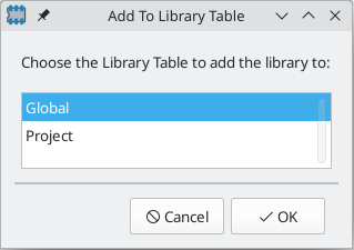
Creating a new footprint library
You can create a new footprint library by clicking File → New Library…. At this point you must choose whether the new library should be added to the global footprint library table or the project footprint library table. Libraries in the global library table will be available to all projects, while libraries in the project library table will only be available in the current project.
Following selection of the library table, you must choose a name and location for the new library. A new, empty library will be created at the specified location.
Creating a new footprint
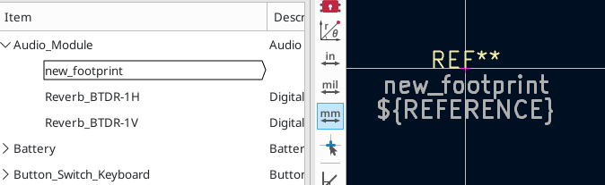
To create a new footprint in the current footprint library, click the ![]() button or click File → New Footprint…. A new, untitled footprint will be created in the selected library.
button or click File → New Footprint…. A new, untitled footprint will be created in the selected library.
To set the name of the footprint, open its properties dialog (![]() button or E). The name will set the name of the footprint, which is used when assigning a footprint to a symbol, and is also used as the filename of the footprint file on disk.
button or E). The name will set the name of the footprint, which is used when assigning a footprint to a symbol, and is also used as the filename of the footprint file on disk.
The new footprint will be empty except for several default text items. The footprint contains two default (mandatory) footprint fields, Reference and Value. Reference contains the text REF**, which will be replaced with the reference designator of the footprint’s corresponding symbol when the footprint is added to the board. Value is initially set to Untitled, which can be changed, but this will also be updated with the contents of the corresponding symbol’s Value field when the footprint is added to the board. Finally, there is a footprint text item containing the string ${REFERENCE}, which is a text variable that will resolve to the value of the footprint’s Reference field once the footprint is on a board.
These items are centered on the footprint’s anchor (origin point), which is indicated with a magenta cross symbol. The anchor can be repositioned (changing the (0, 0) point for the footprint) by selecting the ![]() button and clicking on the new desired anchor position.
button and clicking on the new desired anchor position.
| Rather than manually creating a footprint, for some common footprints you can use a footprint wizard to create a footprint based on a set of parameters. |
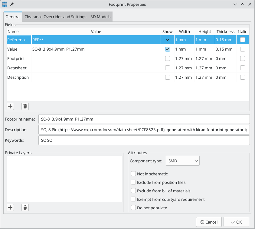
Editing footprint properties
Footprints have a number of properties and metadata items that can be defined. These include text fields, attributes that can be set or not (such as Do Not Populate), clearance and zone connection settings, and 3D model paths. These are initially defined in the library copy of the footprint, but they can be modified on a per-instance basis once a footprint is added to a board. In other words, two copies of the same footprint on a single board can their properties edited separately.
Some properties, namely text fields and attributes, will be automatically set for each footprint in a board based on the fields and attributes in the footprint’s corresponding schematic symbol. Fields and attributes are synced from symbols to footprints when you perform the Update PCB From Schematic action. They are also synced from footprints back to symbols when you perform the Update Schematic From PCB action.
To edit footprint properties, click the ![]() button to show the Footprint Properties dialog. You can also double click an empty spot in the editing canvas.
button to show the Footprint Properties dialog. You can also double click an empty spot in the editing canvas.
Footprint name, description, and keywords
The footprint name, description, and keywords describe the footprint itself. Together they are intended to describe the footprint and help you select an appropriate footprint for each component. They are also used when searching for footprints in the Footprint Editor and the Add Footprint dialog.
The footprint name contains the name of the footprint. This is the same as the footprint’s filename on disk, and is also initially the same as the footprint’s Value field. However, the Value field can be edited in the footprint editor, and when a footprint is added to a board, its Value field will be updated with the value of the footprint’s corresponding symbol.
The description is a description of the footprint. It should be human readable, but it is also used when searching for a footprint.
This description property is specifically a description of the
footprint. This is not to be confused with the Description field,
which will be set to the description of the footprint’s corresponding
symbol when the footprint is added to a board.
|
The keywords are space-separated words related to the footprint. They are used when searching for a footprint.
Footprint fields
Footprints contain multiple fields, which are named values containing information related to the footprint. Fields can be visible and shown on any board layer, or they can be hidden and only shown in the footprint’s properties. Some fields have special meaning to KiCad: Reference and Footprint are both both used by KiCad to identify schematic symbols and PCB footprints, for example. Other fields may contain information that is important for a design but is not interpreted by KiCad, like pricing or stock information for a part.
Any fields defined in a library footprint will be included in the footprint when it is added to a board. You can also add new fields to footprints in the board. Whether they are in the library footprint or not, these fields can then be edited on a per-footprint basis in the board. Symbol fields are also transferred to the board and added as fields in the corresponding footprint.
Footprint fields are different than graphic text. Fields are named, i.e.
they have both a name (Reference) and a value (R101), whereas
footprint text only has a value. Fields can be added to and deleted from
footprints in a board in the Footprint Properties dialog, while text items
can only be added to a footprint in the footprint editor. Fields are also
synced between footprints and their corresponding symbols in the
schematic. Before KiCad version 8.0, footprints did not have named fields,
only graphic text.
|
All library footprints are defined with four default fields which correspond to the default fields in library symbols: Reference, Value, Datasheet, and Description. These default fields cannot be deleted. The Reference field initially has the value REF**, while the Value field is initially set to the name of the footprint. In the board, the values of the four default fields will be set to the values of the matching fields in the footprint’s corresponding symbol.
The Description footprint field is the description of the symbol, not
the footprint, and will be overwritten by the value of the corresponding
symbol’s description. Footprints have a separate footprint description
property (not a field), which is specifically intended for a description
of the footprint.
|
Fields each have an associated layer, which determines which board layer the field will be placed on. Fields can also be visible or hidden.
To edit an existing footprint field, double-click the field, select it or hover and press E, or right-click on the field text and select Properties….
To add new fields, delete optional fields, or edit existing fields, use the ![]() icon on the main tool bar to open the Footprint Properties dialog. Fields can be arbitrarily named, but names starting with
icon on the main tool bar to open the Footprint Properties dialog. Fields can be arbitrarily named, but names starting with ki_, e.g. ki_description, are reserved by KiCad and should not be used for user fields.
Fields have a number of properties, each of which is shown as a column in the properties grid. Not all columns are shown by default; columns can be shown or hidden by right clicking on the grid header and selecting or deselecting columns from the menu.
封装属性
Footprints have several attributes, which are properties of the footprint that affect how it is handled by other parts of KiCad.
Every footprint has a component type: SMD, Through hole, or Unspecified. A footprint’s type affects KiCad’s behavior in a few ways:
-
Footprint type controls the default type of new pads added to the footprint. For through hole and Unspecified footprints, new pads will be through hole by default, although they can be changed after creation. For SMD footprints, new pads will be SMD by default.
-
Footprint type can be used to filter footprints from component placement files as well as other exports, such as STEP files. Additionally, the footprint type is included as metadata in IPC-2581 exports.
-
Footprint 3D models can be shown and hidden in the 3D viewer based on their type. For example, SMD models can be hidden while through hole models are still displayed.
-
Footprints of different types are reported separately in the Board Statistics dialog.
-
DRC will report footprints containing pads that do not match the parent footprint’s type, for example through hole pads in an SMD footprint.
If not in schematic is checked, KiCad will not expect the footprint to correspond to a symbol in the schematic. When updating a PCB from the schematic, KiCad will ordinarily remove footprints that don’t have corresponding symbols according to the delete footprints with no symbols setting. However, such footprints will not be deleted when they have not in schematic set.
If exclude from POS files is checked, KiCad will not include the footprint in component placement file exports.
If exclude from bill of materials is checked, the component will not be included in bill of materials exports in either the schematic or PCB editors. This attribute is synced to and from the footprint’s corresponding schematic symbol.
If exempt from courtyard requirement is checked, the footprint will not trigger a DRC violation if it does not contain a courtyard. Without this attribute set, a footprint without graphics on the F.Courtyard or B.Courtyard layer will cause a "Footprint has no courtyard defined" DRC violation.
The do not populate attribute is primarily a schematic symbol attribute, and is synced to and from the footprint’s corresponding schematic symbol. Footprints with this attribute set can optionally be excluded from component placement file exports and some other types of outputs. These footprints can also be hidden in the 3D viewer.
Private footprint layers
Footprints can have private footprint layers, which are layers that can be viewed and edited in the Footprint Editor but are not shown in the footprint when it is added to a board. Therefore any objects that are on private layers will not be visible in the PCB Editor or included in PCB fabrication outputs. This may be useful, for example, for notes or graphics that are of interest when drawing or editing a footprint but not needed at the board level.
Any of the existing User.* layers (User.Drawings, User.Comments, User.Eco1, User.1, etc.) can optionally be a private layer. To make a layer private, add a private layer in the General tab of the footprint properties dialog, then select the desired layer. Any objects on that layer will not be shown on the board.
Clearance overrides and settings
The Clearance Overrides and Settings tab holds settings for footprint-specific overrides to board clearance and mask/paste expansion, pad-to-zone connections, and net tie settings for allowing pads within the footprint to short different nets.
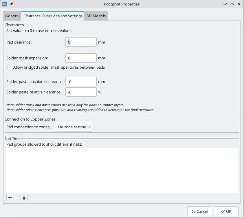
Pad clearance controls the minimum clearance between the footprint’s pads and any copper shape (tracks, vias, pads, zones) on a different net. This value is normally empty, which will cause the pad clearance to be inherited from the board’s design rules and netclass rules. This value can be overridden for individual pads by setting the pad’s clearance to a nonblank value.
Prior to KiCad version 9, a pad clearance of 0 caused the pad clearance value to be inherited.
In KiCad 9 and later, a pad clearance of 0 sets the clearance to 0, while a blank pad
clearance causes the clearance to be inherited.
|
The aperture appearing on any technical layer will have the same shape and size as the pad shape on the copper layer(s). In the PCB manufacturing process, the manufacturer will often change the relative size of mask and paste apertures relative to the copper pad size, but since this size change is specific to a manufacturing process, most manufacturers expect the design data to be provided with the apertures set to the same size as the copper pads. For specific situations where you need to oversize or undersize a technical layer aperture in the design data, you can use the settings here. These values can be overridden for individual pads by setting the pad’s expansion or clearance to a nonzero value.
Solder mask expansion controls the size difference between the pad shape and the aperture shape
on the F.Mask and B.Mask layers. A positive number means the solder mask aperture will be larger
than the copper shape. This number is an inflation applied to all directions. For example, a
value of 0.1mm here will cause the solder mask aperture to be inflated by 0.1mm, meaning that
there will be an 0.1mm border on all sides of the pad and the solder mask opening will be 0.2mm
wider than the pad when measured along a given axis.
Solder paste absolute clearance controls the size difference between the pad shape and the aperture shape on the F.Paste and B.Paste layers. Its behavior is otherwise identical to the behavior of the solder mask expansion setting.
Solder paste relative clearance allows setting a solder paste clearance value as a percentage of the pad size rather than an absolute distance value. If both relative and absolute clearances are specified, they are added together to determine the solder paste aperture size.
Pad connection to zones controls whether the footprint’s pads will have solid, thermal relief, or no connection to zones. Like the other overrides, this one may be set for an individual pad or for an entire footprint. The default setting for this control is From zone setting, which uses the connection mode specified in the connection zones' properties. This setting can be overridden for individual pads by setting the pad’s connection mode to a value other than From parent footprint.
Creating net ties
Footprints can act as net ties, where two separate nets are electrically connected by copper. Connecting nets together would normally causes a DRC error due to violating the clearance between two nets, but a footprint can be configured to short nets without causing a DRC violation. This can be used to connect multiple grounds at a specific location, to make kelvin sense connections to a component, or for other applications.
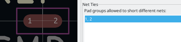
Net ties connect two or more nets in one contiguous region of copper. Each net in a net tie must have its own pad. Pads are not ordinarily allowed to short to other pads; to allow pads to be shorted in net ties, the shorting pads must be added to a net tie group. To create a net tie group, add the pad numbers of the shorting pads to the Net Ties table in the Clearance Overrides and Settings tab of the Footprint Properties dialog. For example, to allow pads 1 and 2 to short in a footprint, add a line to the table with the contents 1,2.
After creating a net tie group, the specified pads are allowed to be electrically shorted. Pads in net tie groups can be connected either by directly overlapping the pads or by adding a copper shape that overlaps both pads.
Footprints can contain multiple net tie groups. Each group can short two or more nets, but every group must remain electrically separate from other groups.
3D models
The 3D Models tab allows you to attach external 3D model files to a footprint and view the footprint in three dimensions along with any attached models.
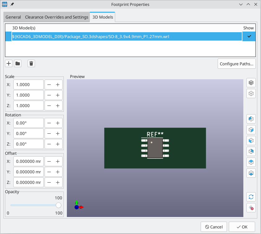
The main part of the window is a 3D preview of the footprint and any attached models. The buttons to the right of the preview let you enable or disable an orthographic projection (![]() ), show or hide the PCB model (
), show or hide the PCB model (![]() ), align the view to one of the six face-aligned perspectives (
), align the view to one of the six face-aligned perspectives (![]() ), and refresh the view (
), and refresh the view (![]() ). The bottom button (
). The bottom button (![]() ) lets you set the thickness of the PCB in the preview.
) lets you set the thickness of the PCB in the preview.
The top of the dialog lets you attach external models. Each added model will be shown in the footprint preview as well as in the full PCB 3D view when the footprint is added to a board. Footprint models can be in STEP, VRML, or IDF format. The models are specified as paths to the model files, which can contain path variables such as ${KIPRJMOD} or ${KICAD9_3DMODEL_DIR}. Click the Configure Paths button to configure path variables. If there is a problem loading a model file from the specified path, an icon in the leftmost column will indicate an error.
KiCad will automatically resolve versioned path variables from
older versions of KiCad to the value of the corresponding variable from
the current KiCad version, as long as the old variable is not explicitly
defined itself. For example, ${KICAD8_FOOTPRINT_DIR} will
automatically resolve to the value of ${KICAD9_FOOTPRINT_DIR} if there
is no KICAD8_FOOTPRINT_DIR variable defined.
|
| Many footprints in KiCad’s standard library do not yet have model files created for them. However, these footprints may contain a path to a 3D model that does not yet exist, in anticipation of the 3D model being created in the future. |
By default, models are added with their origin placed at the footprint’s origin, with no offset, scaling, or rotation. Offset, scaling, and rotation can be applied to a model using the controls to the left of the preview canvas. The model’s opacity can be adjusted using the opacity slider, and the model can be completely hidden by deselecting the show checkbox in the rightmost column of the model table.
Embedding files in footprints
External files can be embedded within a footprint. Embedding a file stores a copy of the file inside the footprint. The footprint can then refer to the embedded copy of the file instead of the external file, which makes the footprint more portable as it doesn’t rely on an external file, although the footprint’s filesize is increased as a result. In footprints this is especially useful for embedding 3D models. Files embedded in a footprint are deduplicated when the footprint is added to a board: if a file is embedded in a footprint, and multiple instances of that footprint are added to the board, only one copy of the file will be embedded, and all of the footprint instances will refer to the same embedded file. Files embedded in a footprint cannot be referred to in the parent board. File embedding is explained in more detail in the Board Setup documentation.
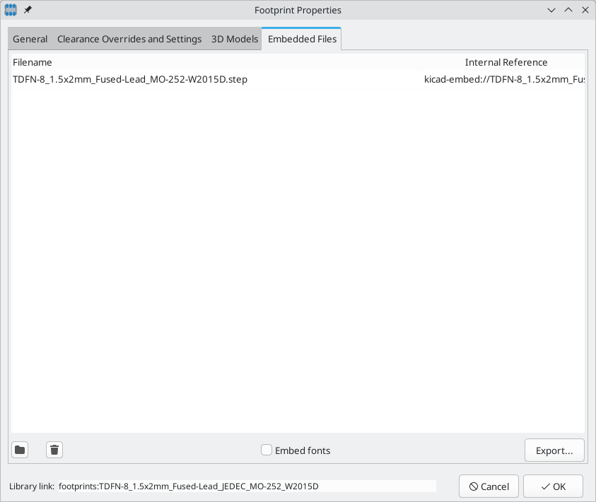
| You can add a 3D model to a footprint and embed it in one step. To do so, add a 3D model in the 3D Models, and enable the Embed File checkbox in the file browser while choosing a model. This embeds the file and automatically uses the embedded reference as the file path instead of the path to the external file. |
Footprint pads
Pads are added to a footprint by clicking the ![]() button in the right toolbar, then clicking again in the desired location in the canvas. The tool continues adding new pads each time you click on the canvas until you cancel the tool (Esc).
button in the right toolbar, then clicking again in the desired location in the canvas. The tool continues adding new pads each time you click on the canvas until you cancel the tool (Esc).
New pads have their pad type set by the footprint’s type, though you can change the pad type later. New pads in SMD footprints are SMD by default, while pads in Through Hole and Unspecified footprints are through hole. Each new pad has its pad number incremented by 1 relative to the previous pad number.
Pad properties
You can edit a pad after adding it by opening the pad’s properties dialog (E). These properties are also editable using the Properties Manager.
General tab
The General tab of the pad properties dialog shows the physical properties of the pad, including its geometry, shape, and layer settings.
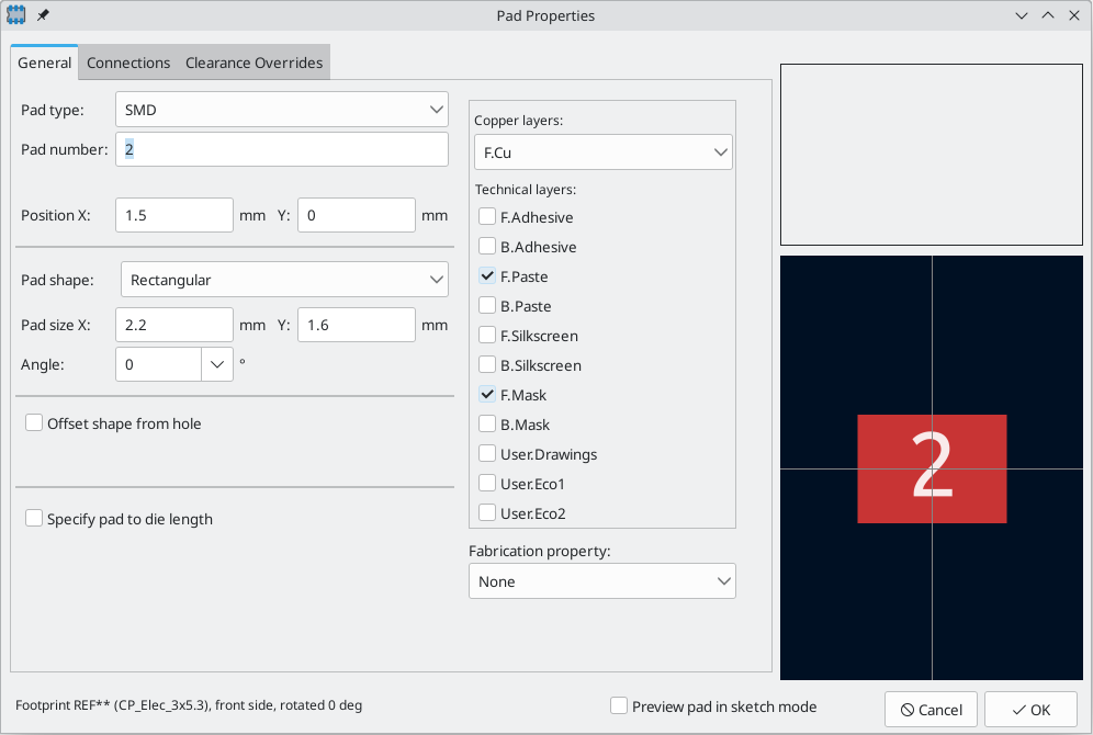
Pad type: this setting controls which features are enabled for the pad:
-
SMD pads are electrically-connected and have no hole. In other words, they exist on a single copper layer.
-
Through-hole pads are electrically-connected and have a plated hole. The hole exists on every layer, and the copper pad exists on multiple layers (see Copper layers setting below).
-
Edge Connector pads are SMD pads that are allowed to overlap the board outline on the
Edge.Cutslayer. -
NPTH, Mechanical pads are non-plated through holes that do not have an electrical connection.
-
SMD Aperture pads are pads that have no hole and no electrical connection. These can be used to add specific designs to a technical layer, for example a paste or solder mask aperture.
铜层 设置控制哪些铜层将有一个与焊盘相关的形状。
For SMD pads, the options are F.Cu or B.Cu, controlling whether the pad sits on the front or the back of the board relative to the footprint’s location. In other words, if a pad is set to exist on B.Cu in its properties, and the footprint is flipped to the back of the board, that pad will now exist on F.Cu, because it also has been flipped.
For through-hole pads, it is possible to remove the pad shape from copper layers where the pad is not electrically connected to other copper (tracks or filled zones). Setting the copper layers to connected layers only will remove the pad shape from any unconnected layers, and setting to F.Cu, B.Cu, and connected layers will remove the pad shape from any internal unconnected layers. This can be useful in dense board designs to increase the routable area on internal layers.
技术层 复选框控制哪些技术层会有一个与焊盘形状相同的孔径。 默认情况下,焊盘在锡膏层和阻焊层上的孔径与铜层相匹配。
| 在当前版本的 KiCad 中,不支持在不同的铜层上定义不同的焊盘形状或尺寸。 |
The Pad number controls what the pad will be electrically connected to in the board. A pad has the same net connection as the pin with the same number in the corresponding schematic symbol.
Pad Position X and Y are the location of the center of the pad, relative to the footprint’s origin.
Pad shape controls the basic shape of the pad. This can be circular, oval, rectangular, trapezoidal, rounded rectangle, chamfered rectangle, chamfered with other corners rounded, custom (circular base), or custom (rectangular base). Each pad shape has its own set of options; for example, rounded rectangles have settings for pad size X and Y, angle, corner size, and corner radius.
| The size of a pad can also be adjusted interactively in the canvas by dragging the editing handles at the pad corners. |
Through-hole and NPTH pads have a hole in addition to the pad itself. The hole shape can be circular or oval, with corresponding size controls. By default the pad is centered on the hole, but the pad can be offset relative to the hole if the offset shape from hole option is enabled (circular pads cannot be offset from the hole).
Fabrication properties are primarily used as metadata in Gerber X2 fabrication output, where the fabrication property is included as an aperture attribute for each pad. Some properties also affect DRC. The following fabrication properties are available:
-
BGA pad can only be applied to SMD pads, and only affects Gerber X2 output.
-
Fiducial, local to footprint and fiducial, global to board only affect Gerber X2 output.
-
Test point can only be applied to SMD or through hole pads, can only be applied to pads on outer layers, and only affects Gerber X2 output.
-
Through hole pads with the heatsink pad property are allowed in SMD footprints (PTH pads without this property cause a DRC violation when they are used in SMD footprints). It also affects Gerber X2 output.
-
The castellated pad property is for pads that intentionally intersect the board edge such that they will be bisected when the board is manufactured. Pads with this property are allowed to intersect the board edge and still be routed (it is otherwise a DRC error for a pad to intersect the board edge, which makes routing impossible). In STEP exports, pads with this property are clipped to the board edge. This property also affects Gerber X2 output.
-
Through hole pads with the mechanical property can be used in SMD footprints without causing a DRC violation. This can be used for mounting pads or other mechanical through hole pads in surface mount footprints. This is similar to the heatsink pad property, but does not affect Gerber X2 output.
-
None is for pads for which none of the other fabrication properties apply. It has no effect.
Specify pad to die length: This setting allows a length to be associated with this pad that will be added to the routed track length by the track length tuning tools and the Net Inspector. This can be used to specify internal bondwire lengths for more accurate length matching, or in other situations where the electrical length of a net is longer than the length of the routed tracks on the board.
Connections tab
The Connections tab contains settings for how pads connect to other objects, including settings for teardrops, zone connections, and thermal reliefs.
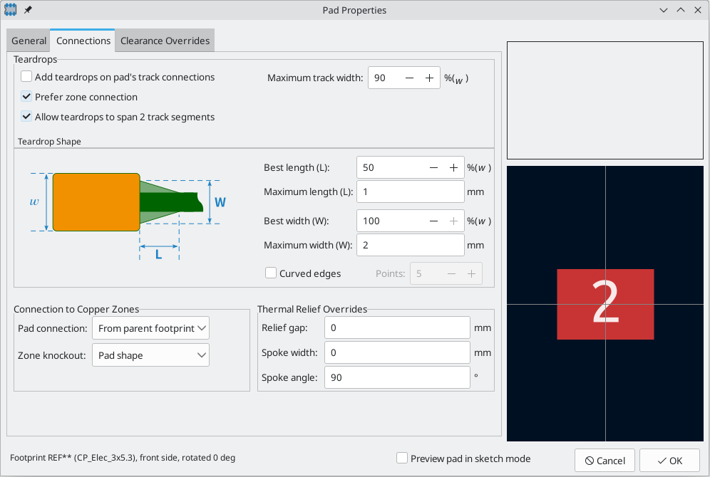
The Teardrops section contains settings controlling teardrop connections between tracks and the pad, if teardrops are used. Teardrop settings are explained in the teardrop documentation.
Pad connection controls whether the pad will have a solid, thermal relief, or no connection to the zone. Like the other overrides, this one may be set for an individual pad or for an entire footprint. The default setting for this control is From parent footprint, and the default footprint setting is to use the connection mode specified in the zone properties.
Zone knockout controls the behavior of the zone filler when the pad uses a custom shape rather than one of the default shapes. This can be used to achieve different results when using thermal reliefs and custom pad shapes.
Relief gap controls the length of the thermal spokes, or the gap between the pad’s shape and the filled copper area of the zone. This value is normally empty which will cause the relief gap to be inherited from the connecting zone’s settings.
Spoke width controls the width of the spokes generated when the zone connection mode is Thermal Relief. This value is normally empty which will cause the spoke width to be inherited from the connecting zone’s settings.
Prior to KiCad version 9, a relief gap or spoke width of 0 caused that value to be inherited.
In KiCad 9 and later, a relief gap or spoke width of 0 sets that value to 0, while a blank
value causes the value to be inherited.
|
Clearance Overrides tab
The Clearance Overrides tab holds settings for pad-specific overrides to board clearance and mask/paste expansion.
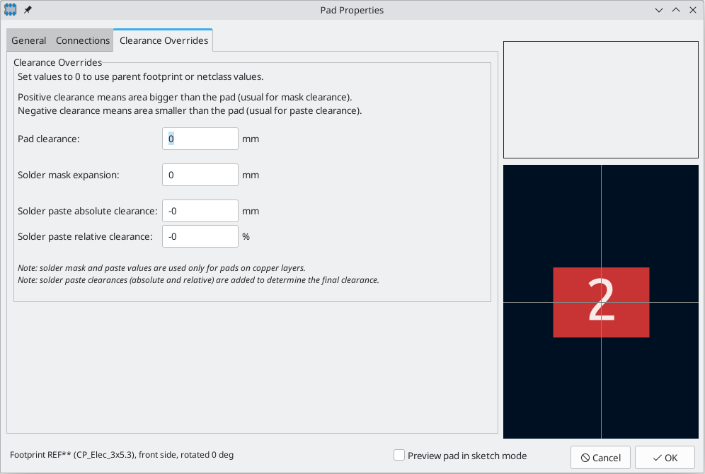
Pad clearance controls the minimum clearance between the pad and any copper shape (tracks, vias, pads, zones) on a different net. This value is normally empty which will cause the pad clearance to be inherited from any clearance override set on the footprint, or the board’s design rules and netclass rules if the footprint clearance is also empty.
Prior to KiCad version 9, a pad clearance of 0 caused the pad clearance value to be inherited.
In KiCad 9 and later, a pad clearance of 0 sets the clearance to 0, while a blank pad
clearance causes the clearance to be inherited.
|
The aperture appearing on any technical layer will have the same shape and size as the pad shape on the copper layer(s). In the PCB manufacturing process, the manufacturer will often change the relative size of mask and paste apertures relative to the copper pad size, but since this size change is specific to a manufacturing process, most manufacturers expect the design data to be provided with the apertures set to the same size as the copper pads. For specific situations where you need to oversize or undersize a technical layer aperture in the design data, you can use the settings here.
Solder mask expansion controls the size difference between the pad shape and the aperture shape
on the F.Mask and B.Mask layers. A positive number means the solder mask aperture will be larger
than the copper shape. This number is an inflation applied to all directions. For example, a
value of 0.1mm here will cause the solder mask aperture to be inflated by 0.1mm, meaning that
there will be an 0.1mm border on all sides of the pad and the solder mask opening will be 0.2mm
wider than the pad when measured along a given axis.
Solder paste absolute clearance controls the size difference between the pad shape and the aperture shape on the F.Paste and B.Paste layers. Its behavior is otherwise identical to the behavior of the solder mask expansion setting.
Solder paste relative clearance allows setting a solder paste clearance value as a percentage of the pad size rather than an absolute distance value. If both relative and absolute clearances are specified, they are added together to determine the solder paste aperture size.
Working with multiple pads
When you place a new pad, the new pad’s properties are copied from the default pad properties. Each time any pad is edited, the pad’s updated properties are stored as the default pad properties, so that new pads will match the properties of the most recently edited pad.
You can directly edit the default pad properties by selecting Edit → Default Pad Properties…, or choose an existing pad to represent the default by right clicking the pad and choosing Copy Pad Properties to Default. New pads will use that pad’s properties as their defaults until a new default is selected, either by editing another pad, editing the default pad properties, or manually copying a different pad’s properties to the default.
There are several ways to update existing pads with the properties of other pads. You can apply the default pad properties to an explicit selection of pads by selecting the desired target pads, right clicking, and choosing Paste Default Pad Properties to Selected from the right click context menu. You can also update other pads with a selected pad’s properties using Push Default Pad Properties to Other Pads…, also in the right click context menu.
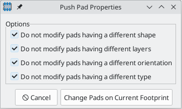
This tool has several options to filter which pads are targeted.
If do not modify pads having a different shape is selected, only pads with the exact same shape properties as the selected pad will be updated.
If do not modify pads having different layers is selected, only pads on the same layer(s) as the selected pad will be updated.
If do not modify pads having a different orientation is selected, only pads with the same orientation as the selected pad will be updated.
If do not modify pads pads having a different type is selected, only pads with the same pad type as the selected pad will be updated.
If no options are selected, all pads in the footprint will be updated.
You can create an array of pads from a source pad by right clicking the source pad and selecting Create from Selection → Create Array… (Ctrl+T). The basic functionality of this tool is described in the PCB Editor documentation. For pads, however, there are additional options for controlling pad numbering.
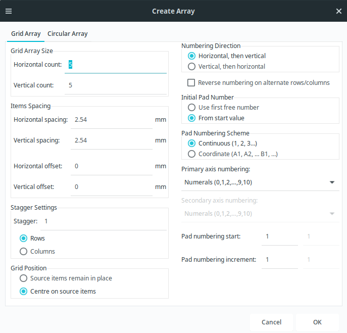
For grid arrays, you can select a numbering direction, either horizontal, then vertical or vertical, then horizontal. If reverse numbering on alternate rows/columns is selected, the direction of increasing pad numbers will alternate from one row/column to the next.
The initial pad number in the array can either be the first unused pad number in the footprint (use first free number) or the specified pad numbering start value. After the first number, the pad numbering can either be continuous (1, 2, 3, …) or coordinate based, in other words, dependent on both the row and column (A1, A2, …, B1, …). In addition to the initial pad number (pad numbering start), you can specify a numbering step (pad numbering skip). For coordinate-based numbering, you can configure separate starting numbers and steps for each axis. You can select whether pad numbers use decimal digits (0-9), hexadecimal digits (0-F), the full alphabet, or the alphabet excepting certain ambiguous letters (I, O, S, Q, X, and Z).
Finally, you can quickly renumber existing pads using the Renumber Pads tool (Edit → Renumber Pads…).
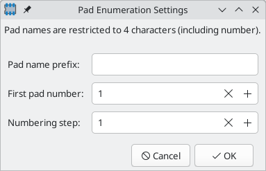
The tool has several options. Pads will be renumbered starting at the selected first pad number, and each subsequent pad will have its number incremented by the numbering step. You can also choose an optional pad name prefix which will be inserted before of the incrementing part of each pad number.
Once you click OK, you will be prompted to click on a pad, which will be assigned a new pad number based on the selected initial pad number and prefix. You can keep clicking on pads to assign them the next number in the sequence based on the selected numbering step. Double click on a pad to renumber that pad and end the sequence, or press Esc to discard the changes.
自定义焊盘形状
For some footprints, the built-in pad shapes (round, rectangular, etc.) may not be sufficient. In these cases you can construct custom pads with arbitrary shapes using Pad Edit Mode. This mode lets you combine a basic pad with graphic shapes to build a new pad out of the compound shape.
To build a custom pad, first add a regular pad using the pad tool (![]() button). This base pad will become the custom pad’s anchor or snapping point, so be sure to place the pad in the exact location where you want tracks to attach to the pad. The shape and size of the pad do not matter, but the hole, if any, will remain in the final custom pad. In other words, a surface mount base pad will result in a surface mount custom pad, and a through hole base pad will result in a through hole custom pad. The custom pad’s number will be inherited from the base pad.
button). This base pad will become the custom pad’s anchor or snapping point, so be sure to place the pad in the exact location where you want tracks to attach to the pad. The shape and size of the pad do not matter, but the hole, if any, will remain in the final custom pad. In other words, a surface mount base pad will result in a surface mount custom pad, and a through hole base pad will result in a through hole custom pad. The custom pad’s number will be inherited from the base pad.
Next, enter Pad Edit Mode by selecting the base pad, right-clicking, and selecting Edit Pad as Graphic Shapes (Ctrl+E). Add graphic shapes as appropriate to create the desired pad shape. Shapes touching the base pad will be unioned together with the base pad to create the final pad shape.
You can exit Pad Edit Mode by right-clicking and selecting Finish Pad Edit, or pressing Ctrl+E again. When you exit pad edit mode, all shapes that touch the base pad will be combined with the pad. For example, when editing a surface mount pad on F.Cu, any shapes that are on F.Cu and touch the base pad will become part of the custom pad. Any shapes that do not overlap the base pad, or that are on a different layer, will remain separate. If the base pad is a through hole pad, overlapping shapes on F.Cu will be combined in the custom pad. Because through hole pads have the same pad shape on all copper layers, this shape will become part of the custom pad on all copper layers, not just F.Cu. For convenience, Pad Edit Mode dims the color of other pads and all shapes that are not contiguous with the base pad so that you can see which shapes will be included in the custom pad and which will not.
Custom pads can only contain a single base pad. Any additional pads that touch the base pad or the contiguous graphics, whether they have the same or different pad numbers as the base pad, will remain separate pads after the shapes are combined into the custom pad.
| If you would like to add multiple anchors (snapping points) to a custom pad, you can add additional separate pads on top of the custom pad. Create the custom pad as normal, containing the first snapping point, then add additional pads with the same number and place them overlapping the custom pad in the desired snapping locations. They will remain distinct pads and will not be combined with the custom pad, but they will act as additional pad anchors and will be electrically connected to the custom pad. |
To modify an existing custom pad, select it and enter Pad Edit Mode again. You can then continue to edit the component shapes to adjust the pad shape, or change the position of the base pad to adjust the pad anchor.
KiCad automatically chooses a size and location for showing the pad number over the pad. Particularly for unusually shaped pads, the automatically determined size and location may not be optimal. In these cases, you can manually specify a region in which KiCad should draw the pad number by adding a pad number box primitive. To add a number box, enter Pad Edit Mode and add a rectangular shape. In the Properties Manager for the rectangle, check the Number Box checkbox. The rectangle will then be shown as a wireframe, and when you exit Pad Edit Mode it will be used to draw the pad number.
In the board, KiCad will automatically add thermal spokes when connecting the pad to a zone. The thermal spoke settings are determined by the pad, footprint, and zone settings, and the thermal spokes by default connect to the pad anchor. You can override the default thermal spoke placement by adding thermal relief templates to the custom pad. To add a thermal relief template, enter Pad Edit Mode and add a line shape. In the Properties Manager for the line, check the Thermal Relief Template checkbox. In Pad Edit Mode, the line will then be shown as a wireframe, and it will not be shown outside of pad edit mode. If any thermal relief templates are present in the pad, KiCad will not automatically add additional spokes when filling zones; spokes will only be placed where there are thermal relief templates defined in the pad. Thermal relief templates only determine the spoke location: spoke width and relief gap are still defined in the pad, footprint, and/or zone properties, as normal.
Footprint graphics and text
Footprints can contain graphic shapes, text, and dimensions. These objects can be placed on nonphysical layers, like F.Fab or User.Drawings, or they can be placed on layers that will be part of the manufactured circuit board, such as Edge.Cuts or a silkscreen, soldermask, or copper layer. Objects on copper layers can make electrical connections.
Closed shapes on a footprint’s F.Courtyard and B.Courtyard layers will form the footprint’s front and back courtyard, respectively. A courtyard defines the physical extents of a footprint and limits where footprints are allowed to be placed in relation to other footprints. If a footprint’s courtyard overlaps another footprint’s courtyard, a DRC violation will be generated.
Shapes on a footprint’s Edge.Cuts layer will correspond to board edges on any PCB that includes the footprint. Closed shapes will result in cutouts, while unclosed shapes will result in unclosed edges. Unclosed edges must be closed in the full board design.
The buttons on the right toolbar can be used to create:
-
Lines (
 , default hotkey Ctrl+Shift+L)
 -
Arcs (
 , default hotkey Ctrl+Shift+A)
 -
Bezier curves (
 , default hotkey Ctrl+Shift+B)
 -
Rectangles (
 )
) -
Circles (
 , default hotkey Ctrl+Shift+C)
 -
Polygons (
 , default hotkey Ctrl+Shift+P)
 -
Text (
 , default hotkey Ctrl+Shift+T)
 -
Textboxes (
 )
) -
Tables (
 )
) -
Dimensions (
 ), of which several types are available
| You can customize the default style of newly-created text and shape objects in Preferences → Footprint Editor → Default Values. |
Graphical objects and their properties are described in more detail in the PCB Editor documentation.
Bulk editing footprint text and graphics
Properties of text and graphics can be edited in bulk using the Edit Text and Graphics Properties dialog (Edit → Edit Text & Graphic Properties…).
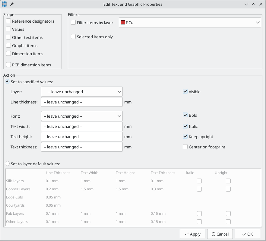
This dialog is described in more detail in the PCB Editor documentation.
Cleaning up footprint graphics
There is a dedicated tool for performing common cleanup operations on graphics, which is run via Tools → Cleanup Graphics….
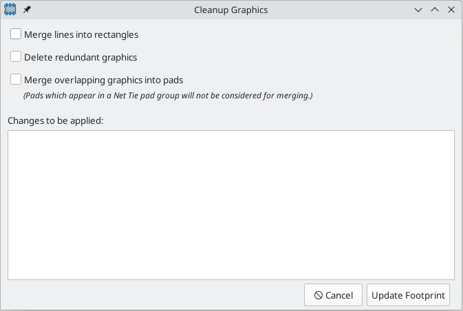
The following cleanup actions are available and will be performed when selected:
Merge lines into rectangles: combines individual graphic lines that together form a rectangle into a single rectangle shape object.
Delete redundant graphics: deletes graphics objects that are duplicated or degenerate.
Merge overlapping graphics into pads: merges graphic copper shapes that overlap pads into a custom pad.
Any changes that will be applied to the footprint are displayed at the bottom of the dialog. They are not applied until you press the Update Footprint button.
Rule areas
Rule areas, also known as keepouts, are footprint regions that can have specific DRC rules defined for them. Some basic rules are available that will raise DRC errors if certain types of objects are within the bounds of the rule area, but rule areas can also be used together with custom DRC rules to define complex DRC behavior that only applies within the rule area. A rule area in a footprint takes effect when the footprint is added to the board.
You can add a rule area by clicking the ![]() button on the right toolbar (Ctrl+Shift+K). Click on the canvas to place the first corner, which will show the Rule Area Properties dialog. After configuring the rule area appropriately, press OK to continue placing corners of the rule area. The rule area shape can be an arbitrary polygon; click on the starting corner or double click to finish placing the rule area.
button on the right toolbar (Ctrl+Shift+K). Click on the canvas to place the first corner, which will show the Rule Area Properties dialog. After configuring the rule area appropriately, press OK to continue placing corners of the rule area. The rule area shape can be an arbitrary polygon; click on the starting corner or double click to finish placing the rule area.
Rule areas are described in more detail in the PCB editor documentation.
Reference images
Just like in the PCB Editor, you can use reference images in the Footprint Editor to assist with your footprint designs. Footprint reference images are only shown in the Footprint Editor: they are not shown in the PCB Editor when a footprint is added to a board, and they do not appear in any fabrication outputs.
To add a reference image, use the ![]() button on the right toolbar and select the desired reference image file.
button on the right toolbar and select the desired reference image file.
Reference images are described in more detail in the PCB Editor documentation.
封装向导
KiCad provides a set of footprint wizards that can be used to create some common kinds of footprints based on a set of parameters. Wizards for the following types of footprints are provided:
-
BGA packages
-
QFN packages
-
QFP packages
-
SOIC, MSOP, SSOP, TSSOP, etc. packages
-
SIP and DIP packages
-
ZIP packages
-
ZOIC packages
-
FPC connectors
-
Micromatch SMD connectors
-
Circular pad arrays
-
Touch sliders
-
Mutual capacitance touch buttons
-
USS-39 barcodes
-
QR codes
To create a footprint using a footprint wizard, click the ![]() button and choose a footprint type from the list that appears.
button and choose a footprint type from the list that appears.
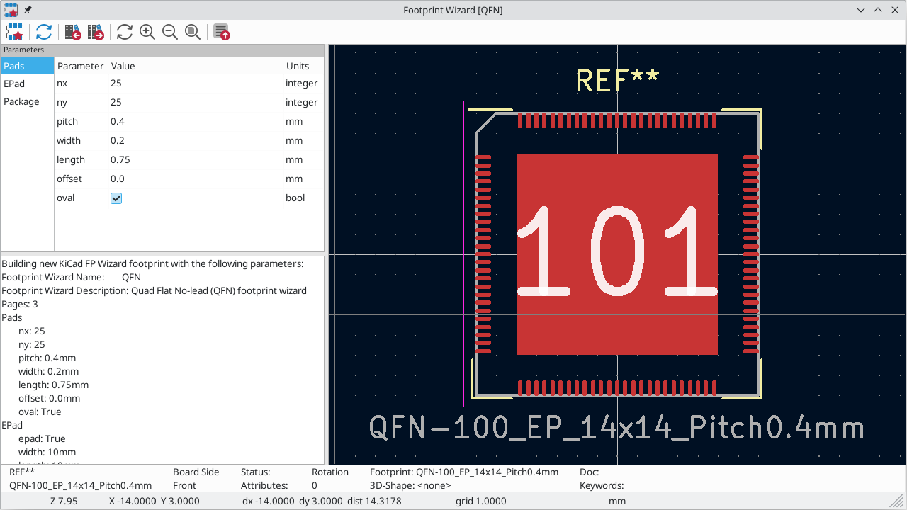
In the window that appears, fill out the parameters as appropriate. When the parameters are correctly filled out, press the ![]() button to transfer the generated footprint back into the footprint editor. Then you can make additional manual modifications and save the footprint as normal.
button to transfer the generated footprint back into the footprint editor. Then you can make additional manual modifications and save the footprint as normal.
In addition to the set of footprint wizards that KiCad provides, you can also create your own. For more information about creating new footprint wizards, see the Scripting section of the Advanced Topics chapter.
Checking footprints
The Footprint Editor can check for common issues in your footprints. Run the footprint checker using the ![]() button in the top toolbar.
button in the top toolbar.
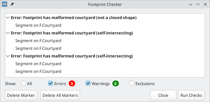
Any footprint issues that are detected are listed in the dialog and displayed with arrow indicators in the editing canvas. Clicking on an issue in the dialog will focus on the issue in the canvas.
The footprint checker checks for:
-
Malformed or missing courtyards
-
Pads that don’t match the footprint’s type: footprints without any through hole pads should be set to the surface mount footprint type
-
Through hole pads without a hole
-
Plated through hole pads not on any copper layers
-
Plated through hole pads without a copper annulus
-
Plated through hole pads with a hole that isn’t fully within the pad
-
Surface mount pads on both the front and back
-
Surface mount pads with mismatched copper and paste/mask layers (front copper and back paste/mask, or vice versa)
-
Pads co-located with or too close to other holes
-
Collisions between silkscreen and solder mask openings
-
Pads that short to other pads outside of net tie groups
-
Nonexistent pads in net tie groups
-
Pads in that appear in multiple net tie groups
Browsing footprint libraries
The Footprint Library Browser allows you to quickly examine the contents of footprint libraries. The Footprint Library Viewer can be accessed by clicking ![]() icon on the main Board Editor toolbar or with View → Footprint Library Browser.
icon on the main Board Editor toolbar or with View → Footprint Library Browser.
To examine the contents of a library, select a library from the list in the left hand pane. All footprints in the selected library will appear in the second pane. Select a footprint name to view the footprint.
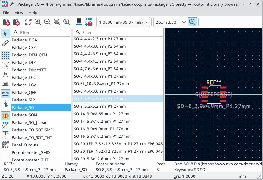
Double clicking the name of a footprint or using the ![]() button adds the footprint to the board.
button adds the footprint to the board.
The top toolbar contains the following commands:
|
Select previous footprint in library. |
|
Select next footprint in library. |
|
Zoom tools. |
|
Open footprint in 3D Viewer. |
|
Add the footprint to the board. |
|
Automatically zoom to fit each opened footprint. |
The left toolbar contains the following commands:
|
Selection tool (the default tool). |
|
Interactively measure the distance between two points. |
|
Turn grid display on/off. |
|
Switch between polar and Cartesian coordinate display in the status bar. |
|
Display/entry of coordinates and dimensions in inches, mils, or millimeters. |
|
Switch between full-screen and small editing cursor (crosshairs). |
|
Show or hide pad numbers. |
|
Switch display of pads between filled and outline mode. |
|
Switch display of text between filled and outline mode. |
|
Switch display of graphic items between filled and outline mode. |