KiCad Nightly Reference Manual
| 本手册正在修订中,以涵盖KiCad的最新稳定发布版本。 它包含一些内容尚未编写完成。 我们希望您能耐心等待我们的志愿技术作者完成这项工作。 同时我们也欢迎新的贡献者加入我们的行列,帮助我们使 KiCad 的文档比以前更好。 |
Copyright
This document is Copyright The KiCad Documentation Contributors. You may distribute it and/or modify it under the terms of either the GNU General Public License (http://www.gnu.org/licenses/gpl.html), version 3 or later, or the Creative Commons Attribution License (http://creativecommons.org/licenses/by/3.0/), version 3.0 or later.
本指南中的所有商标均属于其合法所有者。
Contributors
Jean-Pierre Charras, Fabrizio Tappero, Wayne Stambaugh, Cirilo Bernardo, Jon Evans, Graham Keeth
翻译人员
Qinghan Hu <[email protected]>, 2023.
taotieren <[email protected]>, 2019-2025.
Feedback
The KiCad project welcomes feedback, bug reports, and suggestions related to the software or its documentation. For more information on how to submit feedback or report an issue, please see the instructions at https://www.kicad.org/help/report-an-issue/
Software and Documentation Version
This user manual is based on KiCad 10.99. Functionality and appearance may be different in other versions of KiCad.
Documentation revision: 2e473680.
KiCad PCB 编辑器简介
The KiCad PCB Editor is a PCB layout application distributed as a part of KiCad and available for the following operating systems:
-
Linux
-
Apple macOS
-
Windows
Regardless of the OS, all KiCad files are 100% compatible from one OS to another.
The PCB Editor is an integrated application where all functions of placing footprints, routing tracks, library management, and data transfer to and from the schematic capture software are carried out within the editor itself.
The KiCad PCB Editor is intended to communicate directly with the KiCad Schematic Editor for designing printed circuit boards from schematics without using any intermediate files. It can also import netlist files, which list all the electrical connections, from other packages.
The PCB Editor includes a footprint library editor, which can create and edit footprints and manage libraries. It also integrates the following additional but essential functions needed for modern PCB design software:
-
Design rules check (DRC) for automatic detection of design rule violations such as incorrect and missing connections, copper clearance and minimum width violations, and many other design issues
-
Scriptable design rules for specifying rules with complex constraints and conditions
-
An interactive router with multiple modes of operation (push-and-shove, walkaround, highlight collisions) and support for differential pair routing as well as length and skew tuning
-
Export of fabrication and plot files in many formats (Gerber, IPC-2581, ODB++, GenCAD, PDF, PostScript, and SVG)
-
A 3D viewer and 3D model generation in many formats (STEP, GLB, BREP, XAO, PLY, STL, IDF, and VRML)
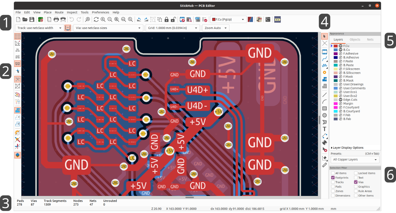
PCB 编辑器的用户界面
PCB 编辑器的主要用户界面如上图所示,并标明了一些关键元素:
-
顶部工具栏 (文件管理、缩放工具、编辑工具)
-
消息面板和状态栏
-
Editing canvas
浏览编辑画布
编辑画布是正在设计的电路板视图。您可以平移和缩放到电路板的不同区域,也可以翻转视图以从底部显示电路板。
默认情况下,用鼠标中键或右键拖动会平移画布视图,滚动鼠标滚轮会放大或缩小视图。 你可以在偏好设置中的鼠标和触摸板部分改变这一行为(详见 配置和定制)。
在顶部的工具栏中,还有其他几个缩放工具可用:
-
 放大视口的中心。
 -
 从视口中心缩小。
 -
 缩放以适应绘图页周围的框架。
 -
 缩放以适应绘图页内的对象。
 -
 允许你画一个方框来确定缩放的区域。
光标的当前位置显示在窗口的底部(X 和 Y),同时显示的还有当前的缩放系数(Z)、光标的相对位置(dx、dy 和 dist)、网格设置和显示单位。
按 Space 可以将相对坐标重置为零。这对于测量两点之间的距离或对齐对象很有用。
快捷键
快捷键 Ctrl+F1 显示当前快捷键列表。默认的快捷键列表包含在本手册的 Actions Reference 部分。
本手册中描述的快捷键使用了标准 PC 键盘上的按键标签。在苹果键盘布局中,使用 Cmd 键来代替 Ctrl,使用 Option 键来代替 Alt。
许多操作默认没有分配快捷键,但可以使用快捷键编辑器(偏好设置 → 偏好设置… → 快捷键 )分配或重新定义快捷键。
| 通过快捷键可用的许多操作也可在上下文菜单中使用。要访问上下文菜单,请在编辑画布中单击鼠标右键。根据选择的内容或处于活动状态的工具,将提供不同的操作。 |
快捷键存储在 KiCad 的配置目录下的 user.hotkeys 文件中。这个位置是特定于平台的:
-
Windows:
%APPDATA%\kicad\10.0\user.hotkeys -
Linux:
~/.config/kicad/10.0/user.hotkeys -
macOS:
~/Library/Preferences/kicad/10.0/user.hotkeys
KiCad 可以使用快捷键编辑器中的 导入快捷键 按钮从 user.hotkeys 文件中导入快捷键设置。
显示和选择控件
板层
PCB 编辑器中的层代表电路板上的物理铜层,以及用于定义丝印、阻焊和电路板边框等的图形层。 在编辑器中,总有一个层是活动的。 活动图层绘制在其他图层之上,并将成为分配给新创建对象的图层。 活动层在顶部工具栏的图层选择器下拉框中显示,在外观面板中也被突出显示。 要改变活动层,你可以左键单击外观面板中的层名,使用顶部工具栏中的下拉层选择器,或使用快捷键。 图层可以被隐藏以简化电路板视图。 你可以隐藏一个层,即使它是活动层。
电路板层的显示顺序
The display order for board layers is dynamic and depends on which layer is selected as the active layer. The active layer is always drawn on top of other layers. In addition, layers that are related to the active layer are drawn on top of layers that are unrelated. For example, if you make B.Silkscreen the active layer, then all of the other back layers (B.Cu, B.Adhesive, B.Paste, B.Mask, B.Fab, and B.Courtyard) will be drawn on top of the front, user, and inner copper layers, with B.Silkscreen topmost. If you make Edge.Cuts active, then it will be drawn on top, and the User.* layers and Margin will also be be brought to the front.
| Selected objects are always drawn on top, even if they are not on the active layer. |
外观面板
外观面板提供了管理 PCB 编辑器绘图画布中的对象的可见性、颜色和不透明度的控制。 它有三个标签:层标签包含电路板层的控制,对象标签包含不同类型图形对象的控制,网络标签包含飞线和铜对象的外观控制。
图层控件
在外观面板的 “层” 选项卡中,每个电路板层都显示了其颜色和可见性状态。 活动层在色块的左边有一个箭头指示器。 左键点击一个图层来选择它作为活动图层。 左键单击相应的可见性图标,在可见和隐藏之间切换该图层。 双击或中击色块来改变该图层的颜色。
| 必须先在偏好选项中创建自定义颜色主题, 然后才能在“外观”面板中更改图层颜色。 |
在图层列表下方是一个包含图层显示选项的可展开面板。第一个设置控制非活动图层的显示方式:正常、暗显或隐藏。层显示模式可用于简化视图并聚焦于单个层。当非活动层显示模式为 "暗显" 或 "隐藏" 时,不能选择非活动层上的对象。您可以使用快捷键 Ctrl+H 快速切换这些显示模式。
Flip board view will show the board as if you are looking from the bottom (that is, mirrored around the Y-axis). This option is also available in the View menu.
| 翻转电路板视图不会更改可视层顺序,活动层将保持在最前面,其他层按正常顺序紧随其后。 |
对象控件
外观面板的 "对象" 选项卡与 "图层" 选项卡类似。 主要区别在于,有些对象没有颜色设置,而四种类型的对象(布线、过孔、焊盘和敷铜)有不透明度控制滑块。 这里的不透明度设置将与图层颜色中设置的任何不透明度相乘。 默认情况下,所有对象都是完全不透明的,除了敷铜,敷铜被设置为半透明,以便通过敷铜区域更容易看到对象。
图层预设
图层预设存储了哪些图层和对象是可见和隐藏的,以便于调用。 有几个内置的图层预设,您也可以保存您自己的自定义预设。 自定义预设存储在一个电路板的工程设置中,因为预设可能是特定于某个电路板的层叠。
要加载一个预设,请从外观面板底部的预设下拉菜单中选择它,或者通过按住 Ctrl 并按 Tab 来使用快速切换器。 一旦快速切换器窗口出现,你可以按 Tab 和 Shift+Tab 来循环浏览可用的预设。 当你放开 Ctrl 键时,高亮显示的预设将被加载。
To save a custom preset, first use the visibility controls to choose which layers you want visible, then choose Save preset… from the Presets drop-down menu. Give your preset a name and it will now be available via the drop-down menu and the quick switcher. To modify a custom preset, follow the same process and save the modified version with the same name to overwrite the existing version. To delete a custom preset, choose the Delete preset… option from the drop-down menu and select the preset to be deleted from the list.
Viewports
Viewports store the current view location and zoom level so you can quickly switch back to it later, or switch between several saved views.
To load a viewport, choose it from the Viewports drop-down menu at the bottom of the appearance panel or use the quick switcher by holding down Shift and pressing Tab. Once the quick switcher window appears, you can press Tab to cycle through the stored viewports. When you let go of the Shift key, the highlighted viewport will be loaded.
To save a new viewport, scroll and zoom to show the desired area of the board, then choose Save viewport… from the Viewports drop-down menu. Give your viewport a name and it will now be available via the drop-down menu and the quick switcher. To modify an existing viewport, save a new viewport with the same name to overwrite the existing version. To delete a viewport, choose the Delete viewport… option from the drop-down menu and select the preset to be deleted from the list.
网络和网络类控件
外观面板的网络选项卡显示电路板中所有网络和网络类的列表。每个网络都有一个可见性控件,用于控制该网络在飞线中的可见性。在飞线中隐藏网络不会改变电路板的连接性,也不会影响设计规则检查器;这只是为了使飞线更容易理解。
Each net and net class can also have a color assigned. By default, this color applies to the ratsnest lines for the net (or for all the nets in the net class). Nets have no color by default; this is indicated by a checkerboard pattern in the color swatch. Double-click or right-click a net or net class color swatch to set the color. To give a net class the same color it has in the schematic, right click the net class and select Use color from schematic.
| 默认网络类不能分配颜色, 因为该类中的网络将仅使用颜色主题定义的默认飞线颜色。 |
您还可以通过外观面板选择并高亮网络和网络类:右击网络或网络类以在菜单中显示这些选项。
网络类列表下面是一个包含网络显示选项的可扩展面板。第一个选项控制如何应用网络颜色。当选择了 “所有” 时,属于网络或网络类的所有铜对象 (焊盘、布线、过孔和敷铜) 都将呈现所选的颜色。当选中 “飞线” (默认值)时,只有飞线受网络和网络类颜色的影响。 当选择 “无” 时,网络和网络类颜色被忽略。
第二个选项控制如何绘制飞线。“所有图层” 表示将在所有未连接的项目之间绘制飞线。“可见层” 意味着不会向隐藏层上的项目绘制任何最新的飞线,即使这些项目是未连接的。
| You can configure the thickness of ratsnest lines in the PCB Editor Editing Options section of the Preferences dialog, to make the ratsnest more or less visible. |
选择和选择筛选器
Selecting items in the editing canvas is done with the left mouse button. When no tool is active, single-clicking on an object will select it. Pressing Esc will always cancel the current tool or operation and return to the selection tool. Pressing Esc while the selection tool is active will clear the current selection.
You can also select items using a rectangle or lasso selection. These tools can be useful for selecting many items at once. You can switch between rectangular and lasso selection modes using the ![]() /
/ ![]() palette in the right toolbar.
palette in the right toolbar.
| To switch between multiple tools in a palette, show the palette by clicking and holding the left mouse button on the tool icon or by clicking and dragging the mouse from the tool icon. Release the mouse button on the desired tool to choose it. |
With the rectangular selection mode active (![]() ), clicking and dragging will perform a rectangular selection. A rectangular selection from left to right will only select items that are fully inside the box. A rectangular selection from right to left will select any items that touch the box. A left-to-right selection box is drawn in yellow, with a cursor that indicates exclusive selection, and a right-to-left selection box is drawn in blue with a cursor that indicates inclusive selection.
), clicking and dragging will perform a rectangular selection. A rectangular selection from left to right will only select items that are fully inside the box. A rectangular selection from right to left will select any items that touch the box. A left-to-right selection box is drawn in yellow, with a cursor that indicates exclusive selection, and a right-to-left selection box is drawn in blue with a cursor that indicates inclusive selection.
With the lasso selection mode active (![]() ), clicking and dragging will begin a lasso selection. Any items in the existing selection are deselected. Dragging with the left mouse button held draws a freeform shape. Releasing the button stops drawing the freeform shape and starts drawing a straight line. Clicking again completes the straight line. Any number of freeform or straight segments can be drawn by repeatedly clicking or dragging. Double click to finish drawing the lasso. Similar to a rectangular selection, a lasso drawn in a clockwise direction will only select items that are fully inside the lasso. A lasso drawn in a counter-clockwise direction will select any items that touch the lasso. A clockwise lasso is drawn in yellow, with a cursor that indicates exclusive selection, and a counter-clockwise lasso is drawn in blue with a cursor that indicates inclusive selection.
), clicking and dragging will begin a lasso selection. Any items in the existing selection are deselected. Dragging with the left mouse button held draws a freeform shape. Releasing the button stops drawing the freeform shape and starts drawing a straight line. Clicking again completes the straight line. Any number of freeform or straight segments can be drawn by repeatedly clicking or dragging. Double click to finish drawing the lasso. Similar to a rectangular selection, a lasso drawn in a clockwise direction will only select items that are fully inside the lasso. A lasso drawn in a counter-clockwise direction will select any items that touch the lasso. A clockwise lasso is drawn in yellow, with a cursor that indicates exclusive selection, and a counter-clockwise lasso is drawn in blue with a cursor that indicates inclusive selection.
The selection action can be modified by holding modifier keys while clicking or dragging. Modifiers cannot be used with lasso selections.
The following modifier keys apply when clicking to select single items:
| Modifier Keys (Windows) | Modifier Keys (Linux) | Modifier Keys (macOS) | Selection Effect |
|---|---|---|---|
Ctrl |
Ctrl |
Cmd |
Toggle selection. Note: Ctrl+click can be remapped to highlight net in Preferences → PCB Editor → Editing Options. |
Shift |
Shift |
Shift |
Add the item to the existing selection. |
Ctrl+Shift |
Ctrl+Shift |
Cmd+Shift |
Remove the item from the existing selection. |
long click |
long click or Alt |
long click or Option |
Clarify selection from a pop-up menu. |
The following modifier keys apply when dragging to perform a rectangular selection:
| Modifier Keys (Windows) | Modifier Keys (Linux) | Modifier Keys (macOS) | Selection Effect |
|---|---|---|---|
Ctrl |
Ctrl |
Cmd |
Toggle selection. |
Shift |
Shift |
Shift |
Add item(s) to the existing selection. |
Ctrl+Shift |
Ctrl+Shift |
Cmd+Shift |
Remove item(s) from the existing selection. |
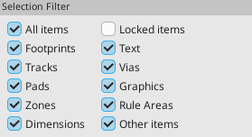
The selection filter panel in the lower right corner of the PCB Editor window controls which types of objects can be selected with the mouse. Turning off selection of unwanted object types makes it easier to select items in a dense board.
The All items checkbox is a shortcut to turn the other items on and off. The Locked items checkbox is independent of the rest, and controls whether or not items that have been locked can be selected. You can right-click any object type in the selection filter to quickly change the filter to only allow selecting that type of object.
If you repeatedly try to select an object whose type is disabled in the selection filter, the selection filter will visually flash the checkbox for that object type as a reminder that selecting that object type is disabled.
When a connected copper item is selected, you can expand the selection to other copper items of the same net using the Expand Selection command in the right-click context menu or with the hotkey U. The first time you run this command, the selection will be expanded to the nearest pad. The second time, the selection will be expanded to all connected items on all layers. Expanding a selection obeys the selection filter, so the expansion will stop when it reaches an object whose type is disabled in the selection filter. For example, if via selection is disabled in the filter, you can expand a selection until a via is reached.
选择一个对象会在窗口底部的信息面板上显示该对象的信息。双击一个对象可以打开一个窗口来编辑该对象的属性。
网络高亮
电气网络(或一组网络)可以在 PCB 编辑器中被高亮显示,以显示该网络是如何在 PCB 上布线的。 通过在 PCB 编辑器中选择要高亮的网络,或者在启用交叉探测高亮时在原理图编辑器中选择相应的网络,可以激活网络的高亮(见下文)。 当网络高亮激活时,高亮的网络将以较亮的颜色显示,所有其他对象将以比正常颜色更暗的颜色显示。
There are several ways to select a net or nets to highlight in the PCB editor:
-
Use the hotkey ` after selecting a copper object, or while hovering over a copper object
-
Right click a copper object in the editing canvas and select Net Inspection Tools → Highlight Net
-
Right click a net in the Nets tab of the Appearance panel and select Highlight
-
Double click a net in the Net Inspector
When you press the Highlight Net hotkey, the nets of any selected copper items will be highlighted. If no copper items are selected, the net of the copper item under the editor cursor will be highlighted.
Net highlighting can be cleared by using the Clear Net Highlight action (hotkey ~) or by using the Highlight net tool on an empty region in the board. By default, Esc also clears net highlighting, but this can be disabled if desired in Preferences → PCB Editor → Editing Options.
选择一个或多个网络进行高亮时,左侧工具栏上的切换网络高亮显示操作将被激活(也可通过快捷键 Ctrl+` 访问)。此操作将打开或关闭高亮,而无需选择要高亮的新网络。
从原理图交叉探测
KiCad 允许在原理图和 PCB 之间进行双向交叉探测。 有几种不同类型的交叉探测。
Selection cross-probing allows you to select a symbol or pin in the schematic to select the corresponding footprint or pad in the PCB (if one exists) and vice-versa.
Cross-probing also works in the 3D Viewer. When a component is selected in the 3D Viewer, it is also selected in the schematic and PCB, and when a component is selected in the schematic or PCB, it is also selected in the 3D Viewer.
By default, cross-probing will result in the display centering on the cross-probed item and zooming to fit. You can disable the centering and zooming behavior, or disable selection cross-probing entirely, in the Display Options section of the Preferences dialog. When the Flash cross-probed selection setting is enabled, selection cross probing will cause the cross-probed item to flash three times, making it easier to spot.
Even when selection cross-probing is disabled, you can manually cross-probe from the schematic to the PCB by right-clicking an object and selecting Select on PCB, or from the PCB to the schematic by right-clicking an object and choosing Select → Select on Schematic.
Highlight cross-probing allows you to highlight a net in the schematic and PCB at the same time. If the option "Highlight cross-probed nets" is enabled in the Display Options section of the Preferences dialog, highlighting a net or bus in the schematic editor will cause the corresponding net or nets to be highlighted in the PCB editor.
左侧工具栏显示控件
左侧的工具栏提供了改变 PCB 编辑器中对象显示的选项。
Some toolbar buttons have more than one item available in a palette. These buttons are indicated with a small arrow in the lower-right corner of the button: 
To show the palette, you can click and hold the mouse button on the button or click and drag the mouse. The palette will show the most selected item when it is closed.
The default contents of the left toolbar are shown below.
| You can edit the toolbar’s contents in the Toolbar page of the PCB Editor Preferences. |
|
Turns grid display on/off. Note: by default, hiding the grid does not disable grid snapping. This behavior can be changed in the Display Options section of Preferences. |
|
Turns item-specific grid overrides on/off. |
|
Switch between polar and Cartesian coordinate display in the status bar. |
|
Display/entry of coordinates and dimensions in inches, mils, or millimeters. Clicking the button toggles to the next unit, or you can choose a unit directly by expanding the palette (click and hold/drag). |
|
Switches the cursor crosshair between small, fullscreen, and 45-degree-rotated fullscreen. Clicking the button toggles to the next crosshair type, or you can choose a crosshair directly by expanding the palette (click and hold/drag). |
|
Switches the line mode between free angle, 90 degree mode, and 45 degree mode for placement of new tracks, zones, graphical shapes, dimensions, and other objects. Clicking the button toggles to the next line mode, or you can choose a line mode directly by expanding the palette (click and hold/drag). You can also toggle between line modes using Shift+Space. |
|
Turns the ratsnest display on/off. |
|
Switches between straight and curved ratsnest lines. |
|
Switches the non-active layer display mode between Normal and Dim. Note: this button will be highlighted when the non-active layer display mode is either Dim or Hide. In both cases, pressing the button will change the layer display mode to Normal. The Hide mode can only be accessed via the controls in the Appearance Panel or via the hotkey Ctrl+H. |
|
When a net has been selected for highlighting, switches the highlighting on or off. Note: this button will be disabled when no net has been highlighted. To highlight a net, use the hotkey `, right-click any copper object in the net and choose Highlight Net from the Net Tools menu, or right-click the net in the list in the Nets tab of the Appearance panel. |
|
Show zone filled areas. |
|
Show zone outlines only. |
|
Switches display of pads between filled and outline mode. |
|
Switches display of vias between filled and outline mode. |
|
Switches display of tracks between filled and outline mode. |
|
Shows or hides the Appearance and Selection Filter panels on the right side of the editor. |
|
Shows or hides the Properties Manager panel on the left side of the editor. |
创建 PCB
PCB 的基本概念
KiCad 中的印刷电路板通常由代表电子元件及其焊盘的 封装、定义这些焊盘如何彼此连接的 网络、形成每个网络中焊盘之间的铜连接的 布线、过孔 和 敷铜 以及定义电路板边缘、丝印标记和任何其他所需信息的各种图形形状组成。
KiCad 通常会将 PCB 上的网络信息与相关的原理图保持同步,但也可以直接在 PCB 编辑器中创建和编辑网络。
性能
KiCad 能够创建多达 32 个铜层、14 个技术层 (丝印、阻焊、元件粘合剂、锡膏等) 和 13 个通用绘图层的印刷电路板。
KiCad 中所有对象的内部测量分辨率为 1 纳米,测量值以 32 位整数存储。 这意味着可以创建最大约 4 米乘 4 米的电路板。
KiCad 目前支持每个工程/原理图一个电路板文件。
从原理图开始
Creating a board from a schematic is the recommended workflow for KiCad. When you create a new project, KiCad will generate an empty board file with the same name as the project. To start designing the board after you have created a schematic, simply open the board file. You can do this either from the KiCad project manager, or by clicking the "Open PCB in board editor" button in the schematic editor. To import the schematic design information into the board editor, including footprints and net connections, use the Tools → Update PCB from Schematic… action (F8). You can also use the ![]() icon in the top toolbar.
icon in the top toolbar.
| 从原理图更新 PCB 是将设计信息从原理图转移到 PCB 的首选方法。在旧版本的 KiCad 中,相应的过程是将网表从原理图编辑器中导出并导入到电路板编辑器中。现在已经没有必要使用网表文件了。 |
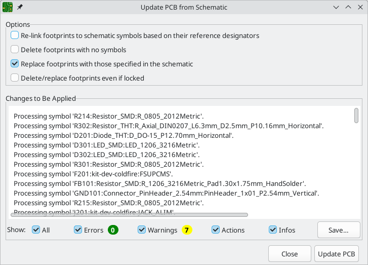
关于从原理图更新PCB工具的更多信息,请参见手册的 [正向批注,正向批注] 部分。
从头开始
也可以创建一个没有匹配原理图的电路板,不过这种工作流程有一些限制,不建议大多数用户使用。为此,您必须独立启动 PCB 编辑器(而不是从 KiCad 工程管理器启动)。在开始设计之前,最好先保存电路板文件,这也将创建一个项目文件来存储电路板设置。 使用文件菜单中的 "另存为… " 来选择保存电路板文件的位置。一个具有相同名称的项目文件将被创建在你选择保存电路板文件的相同位置。
电路板设置
在开始设计电路板之前,使用电路板设置对话框来配置电路板的基本参数。要打开电路板设置,请单击顶部工具栏中的 ![]() 图标或从文件菜单中选择 "电路板设置…"。
图标或从文件菜单中选择 "电路板设置…"。
配置电路板层叠和物理参数
The Board Stackup section of Board Setup is used to configure the stackup and layers of the board.
Board editor layers
The Board Editor Layers page lets you rename layers, disable non-copper layers that will not be used in the design, and add additional user-defined layers for documentation or other purposes. For example, if you will not use a back silkscreen on the design, uncheck the box next to the B.Silkscreen layer. Some layers, like copper layers, courtyard layers, and Edge.Cuts, are required layers and therefore cannot be disabled.
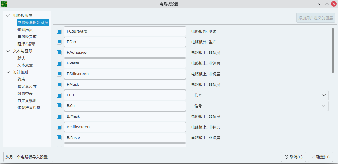
| 在电路板编辑器层部分,可以将铜层指定为信号层、电源层、混合层或跳线层。 本指南仅供用户参考。 无论在此对话框中将类型配置为什么,都可以在任何铜层上布线和敷铜。 |
You can add additional user-defined layers (User.1, User.2, etc.) by clicking the Add User Defined Layer… button in the top right. User-defined layers can’t be used for routing, but they can contain arbitrary graphics or other information. By default, user layers are auxiliary layers, meaning that whatever information they contain does not correspond to either the front or back of the board. User layers can instead be set to Off-board, front or Off-board, back, in which case they correspond to the selected side of the board. Items on such layers can be flipped from front to back in the same way as objects on physical front/back layers. Adjacent front/back layers are treated as paired: if User.2 is defined as a front layer and User.3 is defined as a back layer, flipping an object on User.2 will move it to User.3, and vice versa.
Physical stackup
The Physical Stackup page controls the board layers that are part of the PCB layer stackup: copper layers, dielectric layers, solder mask, and silkscreen.
| Use the Board Editor Layers page to add non-physical layers, configure names for all layers, and enable or disable optional layers. |
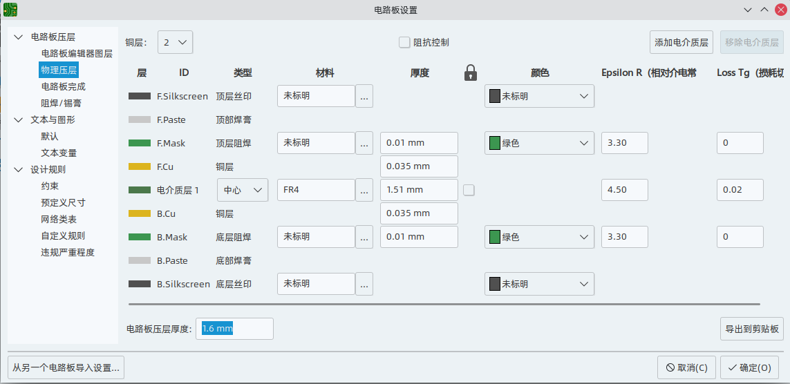
Set the number of copper layers in the upper left corner and then enter the physical parameters of the stackup if desired. These parameters may be left at their default values, but note that the board thickness value will be used when exporting a 3D model of the board, and layer thicknesses will be included in net length calculations for any nets that include vias. If you plan to use these features, it is a good idea to ensure that the stackup thickness is correct. Dielectric, soldermask, and silkscreen layers can have colors assigned to them, which affects the board’s appearance in the 3D viewer and in 3D model exports.
| KiCad 目前仅支持铜层数为偶数的层叠。 要创建具有奇数层的设计 (例如,柔性印刷电路板或金属芯印刷电路板), 只需选择下一个最高的偶数,而忽略多余的层。 |
The Board thickness from stackup value at the bottom of the page is automatically calculated based on the stackup parameters in the table. You can automatically adjust the thickness of dielectric layers by pressing the Adjust Dielectric Thickness button and entering an overall thickness for the PCB. The thickness of the dielectric layers will be adjusted to meet the overall PCB thickness. Any dielectric layers that are locked (the ![]() column is checked) will not be adjusted.
column is checked) will not be adjusted.
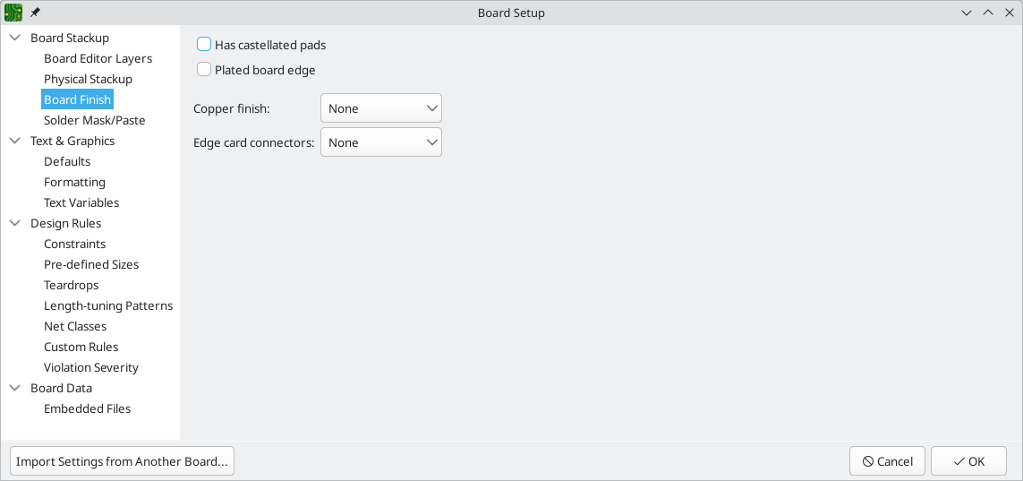
Board finish
The Board Finish section has settings for defining the copper finish and special features such as castellations or edge plating. Note that these settings only impact the board attributes output as part of Gerber job files at this time.
Solder mask/paste
The Solder Mask/Paste section allows global adjustment of the clearance (positive or negative) between solder mask / solder paste shapes and the copper shapes of the parent pads. These values are global settings, but they will be superseded by any clearance overrides set on individual footprints or pads. Positive clearance values will result in the shape of the solder mask or paste opening being larger than the copper shape. Negative clearance values will result in the opening being smaller than the copper shape.
| 大多数商业 PCB 制造商希望这些值为零,并在 CAM 过程中自行调整阻焊和锡膏开口。 通常最好将这些值保留为默认值零, 除非您自己制作 PCB, 或者您的制造商有具体建议使用不同的值。 |
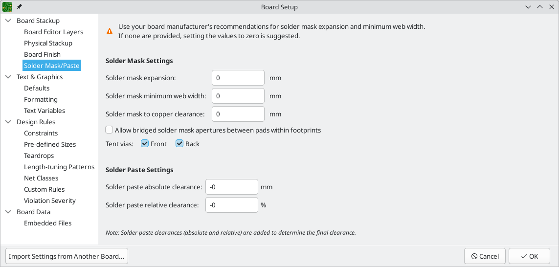
-
Solder mask expansion is a global setting to specify the size of a solder mask opening relative to the parent pad size. If it is
0, solder mask openings will be the same size as the pad. Positive values mean solder mask openings will be larger than pads. Negative values mean solder mask openings will be smaller than pads. This global value is overridden by expansion settings in individual footprints or pads. -
Solder mask minimum web width is the minimum width of webs between solder mask openings, or in other words, the minimum distance between solder mask openings. Any solder mask openings that are closer than this minimum distance will be plotted as a single merged opening.
-
Solder mask to copper clearance is the minimum distance between a solder mask opening and copper with a different net than the opening’s parent copper. Distances smaller than this minimum will result in a DRC error.
-
Allow bridged solder mask apertures between pads within footprints controls whether a DRC violation occurs when multiple pads in the same footprint share a single solder mask opening. This situation can occur when multiple solder mask openings are merged due to the minimum solder mask web width setting.
-
Tent vias controls whether vias are tented (covered with solder mask) on the top and bottom layers of the board. Front and back tenting can be controlled independently. Individual vias can override this setting in their via properties.
-
Solder paste clearance is a global setting to specify the solder paste shape relative to the parent pad size (the size difference between the pad shape and the aperture shape on the F.Paste and B.Paste layers). This can be specified as an absolute offset from the pad edge (e.g.
-0.1mm), a value relative to the pad dimension (e.g.-5%), or both (e.g.-0.1mm - 5%). If it is0or blank, the solder paste aperture will be the same size as the pad. Positive values mean solder paste aperture larger than the pad. Negative values mean solder paste aperture smaller than the pad. This global value is overridden by paste clearance settings in individual footprints or pads.
Zone hatch offsets
The Zone Hatch Offsets page lets you configure default per-layer offsets for zone hatch patterns. X and Y offsets can be configured separately. Per-layer hatch offsets can be used to force the hatching grid to be offset from one layer to another, which is required in some applications. You can override these defaults for individual zones in the Properties dialog for the zone.

Configuring text and graphics
The Text & Graphics section contains formatting settings for text objects, graphic shapes, and dimension objects. It also allows configuring project text variables.
Defaults
The Defaults section of the Board Setup dialog is used to configure the properties that will be used for new text and graphic shapes that are placed on the board.
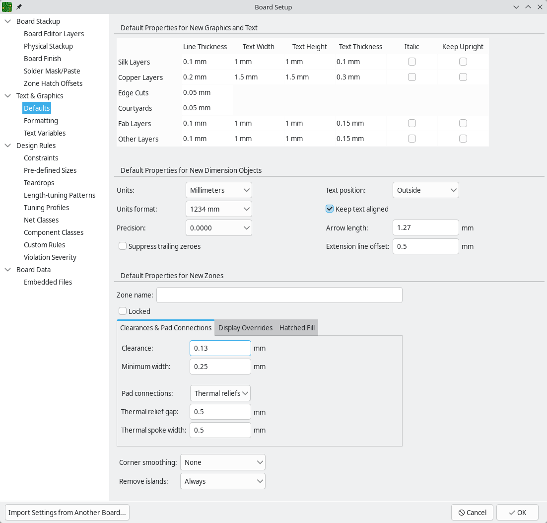
Line thickness, text size, and text appearance can be configured for the six different categories of layers shown in the dialog. These default settings are automatically applied to new text and graphic objects based on the new object’s layer. These settings can be overridden on a per-object basis in that object’s properties, however.
Additionally, the default properties for dimension objects can be configured for all layers. For more details about dimension properties, see the dimensions section.
The Defaults page also contains default settings for new zones. The settings configured here are applied to newly-created zones, but can be overridden on a per-zone basis in the zone’s properties.
Formatting
The Formatting section contains controls for how to format certain board items.
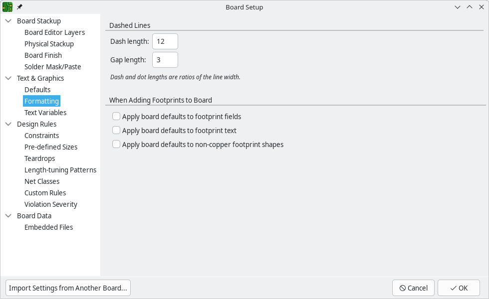
The Dashed Line section controls the appearance of dashed lines. Dash length controls the length of dashes, while Gap length controls the spacing between dashes and dots. The dash and gap lengths are relative to the line width: a gap length of 2 means twice the width of the line.
The checkboxes at the bottom of the page control how the settings from the Defaults page are automatically applied to footprints that are added to the board.
-
Apply board defaults to footprint fields: if checked, default settings will be applied to footprint fields.
-
Apply board defaults to footprint text: if checked, default settings will be applied to footprint text objects.
-
Apply board defaults to non-copper footprint shapes: if checked, default settings will be applied to graphic shapes on non-copper layers in footprints. Graphic shapes on copper layers will not be modified.
-
Apply board defaults to footprint dimensions: if checked, default settings will be applied to footprint dimensions.
-
Apply board defaults to footprint barcodes: if checked, default settings will be applied to footprint barcodes.
文本变量
Project text variables can be created in the Text Variables section. KiCad will substitute the variable name with the text string assigned to the variable. This substitution happens anywhere the variable name is used inside the variable replacement syntax of ${VARIABLENAME}.
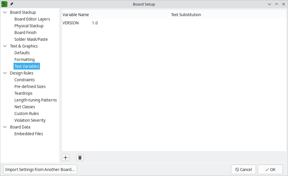
For example, you could create a variable named VERSION and set the text substitution to 1.0. Now, in any text object on the PCB, you can enter ${VERSION} and KiCad will display this as 1.0. If you change the value to 2.0, every text object that includes ${VERSION} will be updated automatically. You can also mix regular text and variables. For example, you can create a text object with the text Version: ${VERSION} which will be displayed as Version: 1.0.
文本变量也可以在 原理图设置 中创建。 文本变量是项目范围内的;在原理图编辑器中创建的变量在电路板编辑器中也可用,反之亦然。
还有一些 内置系统文本变量。
配置设计规则
Design rules control the behavior of the interactive router, the filling of copper zones, and the design rule checker. Design rules can be modified at any time, but we recommend that you establish all known design rules at the beginning of the board design process.
约束
Basic design rules are configured in the Constraints section of the Board Setup dialog. Constraints in this section apply to the entire board and should be set to the values recommended by your board manufacturer. Any minimum value set here is an absolute minimum and cannot be overridden with a more specific design rule. For example, if you need the copper clearance on part of a board to be 0.2mm and in the rest 0.3mm, you must enter 0.2mm for the minimum copper clearance in the Constraints section and use a net class or custom rule to set the larger 0.3mm clearance.
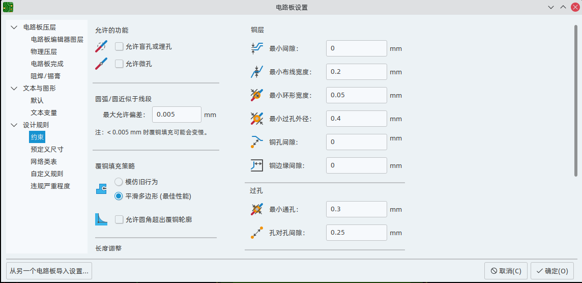
除了设置最小间隙外,还可以在此处配置许多功能:
| Setting | Description |
|---|---|
Arc/circle approximated by segments |
In some situations, KiCad must use a series of straight line segments to approximate round shapes such as those of arcs and circles. This setting controls the maximum error allowed by this approximation: in other words, the maximum distance between a point on one of these line segments and the true shape of the arc or circle. Setting this to a lower number than the default value of 0.005mm will result in smoother shapes, but can be very slow on larger boards. The default value typically results in arc approximation error that is not detectable in the manufactured board due to manufacturing tolerances. |
Allow fillets outside zone outline |
Zones can have fillets (rounded corners) added in the Zone Properties dialog. By default, no zone copper, including fillets, is allowed outside the zone outline. This effectively means that inside corners of the zone outline will not be filleted even when a fillet is configured. By enabling this setting, inside corners of the zone outline will be filleted even though this results in copper from the zone extending outside the zone outline. |
Minimum thermal relief spoke count |
This sets the minimum acceptable number of thermal relief spokes connecting a pad to a zone. A DRC violation will be generated if this constraint is violated. |
Include stackup height in track length calculations |
By default, the length tuner uses the height of the stackup to calculate the additional length of a track that travels through vias from one layer to another. This calculation relies on the board stackup height being correctly configured. In some situations, it is preferable to ignore the height of vias and just calculate the track length assuming that vias add no length. Disabling this setting will exclude via length from length tuner track length calculations. |
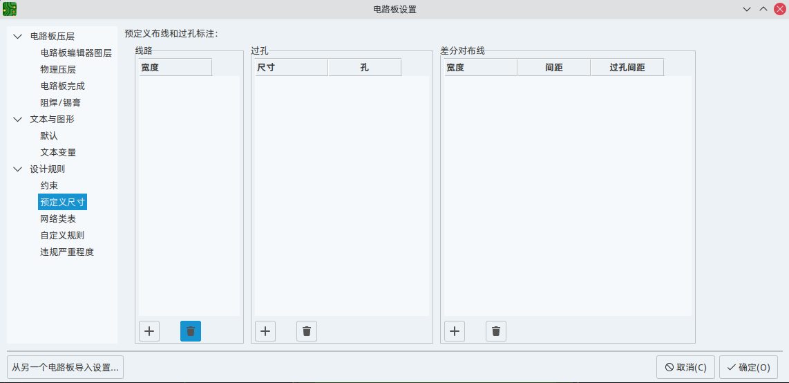
Pre-defined sizes
The Pre-defined Sizes section allows you to define the track and via dimensions you want to have available while routing tracks. Net classes can be used to define the default dimensions for tracks and vias in different nets (see below) but defining a list of sizes in this section will allow you to step through these sizes while routing. For example, you may want the default track width on a board to be 0.2 mm, but use 0.3 mm for some sections that carry more current, and 0.15 mm for some sections where space is limited. You can define each of these track widths in the Board Setup dialog and then switch between them when routing tracks.
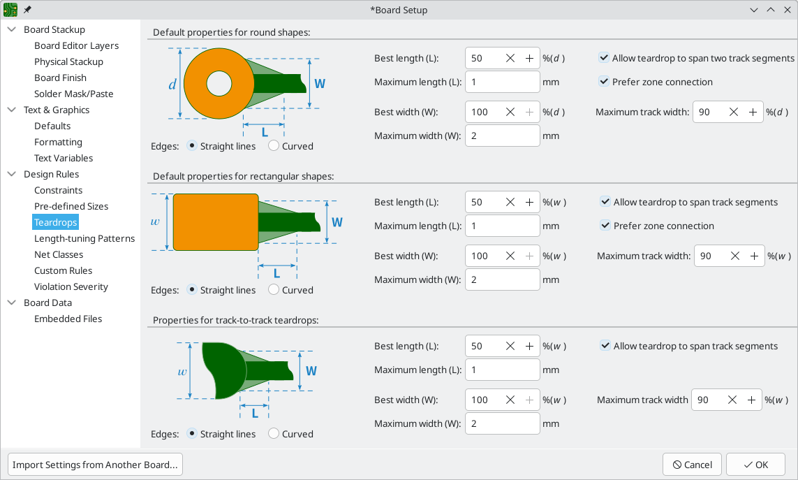
Teardrops
The teardrops section lets you set default parameters for various types of teardrops. There are different settings for teardrop connections to round objects, rectangular objects, and teardrop connections between tracks. The default teardrop parameters can be overridden when teardrops are added, and also changed in the properties for individual connected items. See the teardrops documentation for more information about each setting.
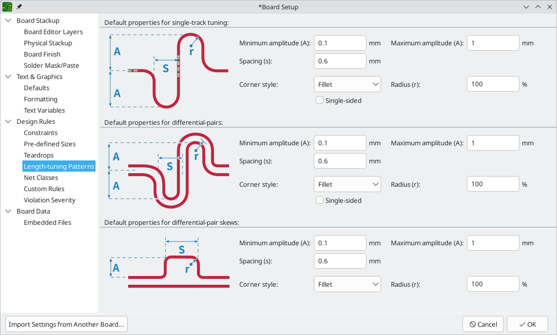
Length-tuning patterns
The length-tuning patterns section lets you set default parameters for each type of length-tuning pattern (single-track length, differential-pair length, and differential-pair skew). These defaults can be overridden in the properties of each tuning pattern added to the board. See the length tuning documentation for more information.
Tuning profiles
Tuning profiles let you define per-layer routing parameters for single-ended and differential tracks with specific impedance requirements. You can automatically calculate track width and gap based on the board stackup and target signal impedance. Tuning profiles can be assigned to net classes, after which the interactive router will use the specified values. DRC can optionally generate violations for tracks that don’t match their tuning profile’s parameters.
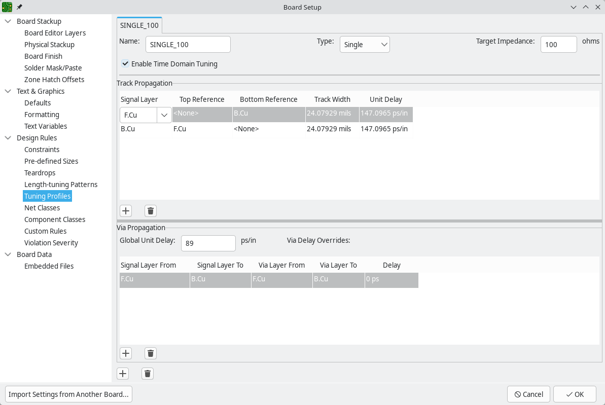
To add a tuning profile, press the ![]() button. You must specify a name for the tuning profile and select whether it applies to single tracks (Single) or differential tracks (Differential). The Target impedance is optional, but required for the tool to calculate track geometry. If Enable time domain tuning is checked, the length tuner will use time domain tuning when tuning tracks assigned this tuning profile; otherwise the tuner will tune based on track length.
button. You must specify a name for the tuning profile and select whether it applies to single tracks (Single) or differential tracks (Differential). The Target impedance is optional, but required for the tool to calculate track geometry. If Enable time domain tuning is checked, the length tuner will use time domain tuning when tuning tracks assigned this tuning profile; otherwise the tuner will tune based on track length.
The Track Propagation section lets you define per-layer track geometries and propagation delays. Each row in the table represents tracks on a different layer. Press the ![]() button below the table to add a new row, or press the
button below the table to add a new row, or press the ![]() button to remove the selected row.
button to remove the selected row.
For each row, you can select the Signal Layer, the Bottom Reference layer, and optional Top Reference layer (for stripline geometries). Each row (signal layer) also has Track Width and Unit Delay values, and differential pairs additionally have a Diff Pair Gap value.
You can enter width, gap, and delay values manually (after calculating them with an external tool) or press the ![]() button in each field to calculate them automatically. The width and gap values are calculated based on the target impedance and the stackup thickness between the signal and reference layer(s). For differential pairs, at least one of the width and gap must be manually entered; the other can be calculated. The delay value is calculated based on the track geometry. The calculator assumes a microstrip or stripline geometry, depending on whether one or two reference layers, respectively, are specified. To use the calculators, you must enter a Target Impedance for the profile and configure the board’s stackup.
button in each field to calculate them automatically. The width and gap values are calculated based on the target impedance and the stackup thickness between the signal and reference layer(s). For differential pairs, at least one of the width and gap must be manually entered; the other can be calculated. The delay value is calculated based on the track geometry. The calculator assumes a microstrip or stripline geometry, depending on whether one or two reference layers, respectively, are specified. To use the calculators, you must enter a Target Impedance for the profile and configure the board’s stackup.
The Via Propagation section lets you define propagation delays for vias. The Global unit delay field is the general propagation delay per unit distance for vias. You can override this general unit delay by adding overrides for individual layer pairs in the table below.
Each row in the table represents vias between specific layer pairs. Press the ![]() button below the table to add a new row, or press the
button below the table to add a new row, or press the ![]() button to remove the selected row.
button to remove the selected row.
Each override has Signal Layer From, Signal Layer To, Via Layer From, and Via Layer To layers. Signal Layer From/To are the layers on which the signal tracks connect to the via. Via Layer From/To are the start and end layers of the full via structure. Through vias start and end at the top and bottom layers of the board. Other types of vias can start and end on inner layers, depending the stackup and via geometry.
Each override also has a Delay value, with which you specify the propagation delay for that type of via.
To remove an entire tuning profile, press the ![]() button at the bottom of the page.
button at the bottom of the page.
You can use tuning profiles to route tracks with specific geometries by assigning the tuning profile to a net class. The interactive router will then use the tuning profile’s geometry values as net class width and differential pair gap values when you route tracks that belong to that net class, the length tuner will use the propagation delays for time-domain tuning, and DRC violations can optionally be generated for tracks that do not match the specified geometry.
To assign a tuning profile to a net class, go to the Net Classes page of Board Setup, then choose a tuning profile in that net class’s Tuning Profile column. You may need to scroll the table or unhide the column in order to see it.
When to enable time-domain tuning
The Enable time domain tuning checkbox controls whether the length tuner operates in time-domain mode (matching propagation delay) or length-domain mode (matching physical trace length) for nets assigned to this tuning profile.
Enable time-domain tuning when:
-
Matched nets are routed on multiple layers with different propagation velocities (e.g., a mix of microstrip and stripline routing).
-
Your design specification defines timing budgets in picoseconds rather than millimeters.
-
Via transitions between layers with different dielectric properties contribute meaningful delay differences that length matching alone cannot capture.
When time-domain tuning is disabled, the tuning profile still provides per-layer track geometry (width and gap) for the interactive router and DRC, but the length tuner matches physical length rather than propagation delay.
You can override the tuning mode on a per-net basis using custom DRC rules.
A length or skew constraint written with time units (e.g., 500ps) will
force the length tuner into time-domain mode for matching nets, regardless of
the tuning profile setting.
|
Understanding track propagation parameters
Each row in the Track Propagation table represents a signal layer and its reference plane(s). The combination of signal layer and reference layer(s) determines the transmission line geometry:
-
One reference layer (bottom reference only): The calculator assumes a microstrip geometry. This is typical for outer layers where the trace sits above or below a single reference plane.
-
Two reference layers (bottom and top reference): The calculator assumes a stripline geometry. This is typical for inner layers where the trace is sandwiched between two reference planes.
The propagation velocity (and therefore the unit delay) differs between microstrip and stripline geometries because the effective dielectric constant is different. Stripline traces are fully enclosed in dielectric material and have a higher effective dielectric constant, resulting in slower propagation (higher unit delay per mm). Microstrip traces are partially exposed to air, resulting in faster propagation (lower unit delay per mm).
The Unit Delay value for each layer is expressed as propagation delay per unit distance (for example, ps/mm). You can enter this value manually if you have calculated it with an external impedance calculator, or press the ![]() auto-calculate button to have KiCad compute it from the board stackup and trace geometry.
auto-calculate button to have KiCad compute it from the board stackup and trace geometry.
|
After making changes to the board stackup (layer thicknesses, dielectric materials),
press the |
Understanding via propagation parameters
The Via Propagation section controls how via delays are calculated in time-domain mode.
The Global unit delay is the default propagation delay per unit distance for all vias. This value is multiplied by the via’s electrical height (the stackup distance between the layers the signal actually uses, not the full via span) to produce the via’s delay contribution.
For more precise control, you can add per-layer-pair overrides in the table below the global delay field. Each override specifies an absolute delay value for a via transition between specific layers. Overrides take priority over the global unit delay calculation.
Each override row has four layer fields:
-
Signal Layer From and Signal Layer To: The copper layers on which the routed tracks connect to the via.
-
Via Layer From and Via Layer To: The start and end layers of the full via structure (e.g.,
F.CuandB.Cufor a through via).
This four-layer specification allows you to define different delays for the same physical via structure depending on which layers the signal actually transitions between.
How tuning profiles, net classes, and the length tuner work together
The relationship between these three features is:
-
A tuning profile defines the per-layer track geometry and propagation delay parameters for a specific impedance target.
-
A net class groups nets that share common routing parameters. Assigning a tuning profile to a net class applies the profile’s geometry and delay values to all nets in that class.
-
The length tuner reads the tuning profile associated with a net’s net class. If the profile has time-domain tuning enabled, the tuner uses the profile’s per-layer delay values to calculate and match propagation delay. If time-domain tuning is not enabled, the tuner falls back to matching physical length.
When the interactive router routes a track belonging to a net class with an assigned tuning profile, it automatically uses the track width and differential pair gap defined in the tuning profile for the current layer. This ensures that the routed geometry matches the assumptions used in the propagation delay calculations.
Net classes
The Net Classes section allows you to configure routing and clearance rules for different classes of nets.
More than one net class can be assigned to a net. For nets with multiple net classes assigned, an effective aggregate net class is formed, taking any net class properties from the highest priority net class which has that property set. Net class priority is determined by the ordering in the Schematic or Board Setup dialogs. The Default net class is used as a fallback for any missing properties after all explicit net classes have been considered; this means that nets may be part of the Default net class even if they have other net classes explicitly assigned.
Net classes may be created and edited in either the Schematic or Board Setup dialogs.
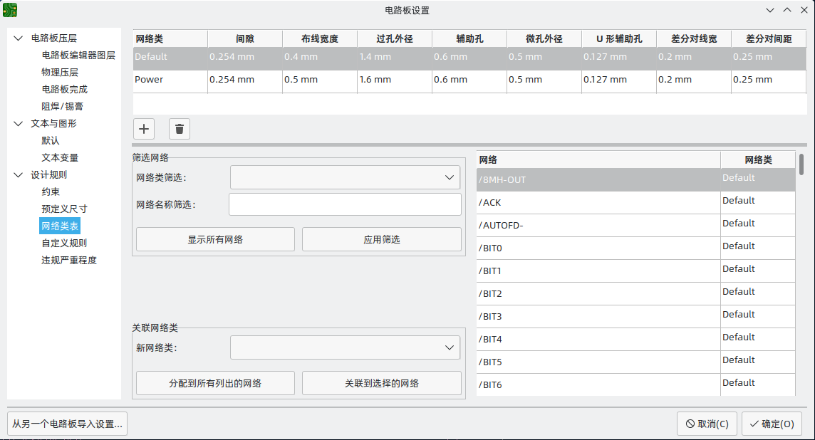
The upper portion of the Net Classes section contains a table showing the net classes in the design and the design rules that apply to each net class. Some columns in the table may be hidden or scrolled to the side. You can show or hide columns in the table by right-clicking on the table header and checking or unchecking columns in the menu.
Every class has values for copper clearance, track width, via sizes, and differential pair sizes. These values will be used when creating tracks and vias unless a more specific rule overrides them (see Custom Rules below).
任何规则都不能覆盖电路板设置的约束条件部分中设置的最小值。
例如,如果您将网络类间距设置为 0.1 mm,但约束条件部分中的最小间距设置为 0.2 mm,
则该类网络的间距将为 0.2 mm。
|
The track widths and via sizes defined for each net class are used when the track width and via size controls are set to "use netclass values" in the PCB editor. These widths and sizes are considered the default, or optimal, sizes for that net class. They are not minimum or maximum values. Manually changing the track width or via size to a different value from that defined in the Net Classes section will not result in a DRC violation. To restrict track width or via size to specific values, use Custom Rules.
You can assign a tuning profile to a net class in the Tuning Profile column. This assigns per-layer track geometry (track width and differential pair gap) and propagation delays for tracks and vias belonging to that net class. Like other net class values, the interactive router uses these values for routing tracks. The length tuner also uses the propagation delays from the tuning profile when tuning tracks in time-domain mode. DRC violations can optionally be generated for tracks that don’t match their tuning profile’s geometry by setting the severity of the "Tuning profile track geometries" violation to either Warning or Error.
Each net class can also have a color assigned to it using the PCB Color column. Depending on how net colors are configured in the appearance panel, net class colors can override the default color for ratsnest lines or copper objects. In addition to arbitrary colors for each net class, you can set all net classes to use the same color as configured for them in the schematic editor by clicking the Import colors from schematic button. To use a layer’s default color instead of overriding it with a custom net class color, set the net class color to transparent.
The lower portion of the Net Classes section lists pattern-based net class assignments. Working with pattern-based net class assignments is explained in the Schematic Editor documentation; pattern-based assignments can be edited in either the Board or Schematic Setup windows.
Note that pattern-based assignments can be created directly from the PCB editing canvas by right clicking a copper track or zone and clicking Assign netclass…. Net classes can also be assigned in the schematic using net class directives or labels instead of pattern-based assignments.
Component classes
The Component Classes section allows you to create rules that automatically assign components to component classes. In addition to these automatic assignments, you can manually assign component classes in the Schematic Editor.
Component classes are named groupings of components: they are assigned to symbols in the schematic or to footprints in the board, but however they are assigned they apply to both the symbols and the corresponding footprints. They can be used to group symbols into channels for multichannel designs and can also be used to group footprints in custom DRC rules. Components can have more than one class.
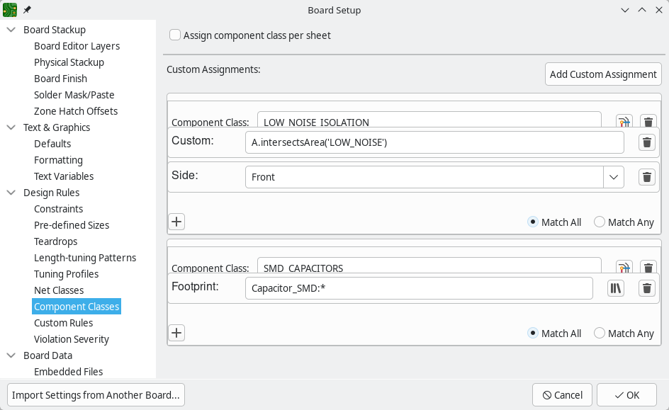
Enabling the Assign component class per sheet will create a component class for every sheet in the schematic and assign each component in the sheet to that sheet’s component class.
You can add a rule for assigning a component class by clicking the Add Custom Assignment button. Enter the name of the component class you want to assign in the Component class textbox, then add a condition for when to assign the class by pressing the ![]() button and selecting a type of condition from the menu that appears.
button and selecting a type of condition from the menu that appears.
The following types of conditions are available:
-
Reference: matches by footprint reference designator. More than one reference designator can be given as a comma-separated list. The reference field support wildcards:
*matches any number of any characters, including none, and?matches any single character. Pressing the button uses the selected footprints' reference designators in the condition.
 -
Footprint: matches by footprint library and identifier. The footprint field support wildcards:
*matches any number of any characters, including none, and?matches any single character. Pressing the button opens a window to choose a footprint from your libraries.
 -
Side: matches by side of the PCB (front, back, or any).
-
Rotation: matches by footprint rotation angle.
-
Footprint Field Value: matches by the value of a specified footprint field. The field name and value support wildcards:
*matches any number of any characters, including none, and?matches any single character. -
Sheet: matches by the name of the schematic sheet containing the footprint’s linked symbol.
-
Custom Expression: matches by a custom DRC rule condition clause, which matches footprints that satisfy the clause. For example,
A.intersectsArea('some_area_name')matches any footprints that intersect the named areasome_area_name.
You can add multiple conditions to a single rule. If Match all is selected, the component class will be assigned to any components that match all of the conditions. If Match any is selected, the component class will be assigned to components that match any of the conditions.
You can test a component class rule by pressing the ![]() button, which highlights all footprints that match the rule in the editing canvas.
button, which highlights all footprints that match the rule in the editing canvas.
To delete a condition, press the ![]() button next to the condition. To delete a rule and all of its conditions, press the
button next to the condition. To delete a rule and all of its conditions, press the ![]() button next to the component class name.
button next to the component class name.
Understanding component classes
A component class is a named label attached to one or more footprints. Unlike net classes, which apply to nets and affect electrical characteristics like clearance and track width, component classes apply to footprints and are used for organizational and rule-scoping purposes.
Common uses for component classes include:
-
Defining channels in multichannel designs
-
Scoping custom DRC rules to specific groups of components
-
Organizing components by function, voltage domain, thermal requirements, or any other design-specific criteria
Where component classes are defined
Component classes can be defined in the schematic editor or in the PCB editor’s Board Setup.
| Definition Method | Editor | Description |
|---|---|---|
|
Schematic |
Assigns the class to all symbols within the rule area. See Schematic Editor: Component Classes. |
|
Schematic |
Assigns the class directly to an individual symbol by adding a |
Assignment rules in Board Setup |
PCB |
Assigns classes to footprints based on conditions such as reference designator, footprint identifier, board side, rotation, field values, sheet membership, or custom DRC expressions. These are configured in Board Setup → Design Rules → Component Classes. |
Automatic sheet-based classes |
PCB |
When Assign component class per sheet is enabled in Board Setup, a component class is automatically created for each schematic sheet and assigned to all components on that sheet. |
Schematic-defined classes are carried to the PCB during Update PCB from Schematic. They persist in the board file and do not change unless the schematic is modified and the PCB is updated from the schematic. PCB-defined classes come from the assignment rules in Board Setup and are re-evaluated whenever the board state changes, for example when a footprint is moved to the other side of the board.
How multiple classes combine
A footprint can belong to more than one component class. When it does, all of the footprint’s class names are sorted alphabetically and displayed as a comma-separated list. For example, a footprint belonging to both Power_Stage and Channel_A is shown as Channel_A, Power_Stage.
You can check a footprint’s component class by selecting it and viewing the Component Class field in the Properties Panel or the status bar.
In custom DRC rules, use A.hasComponentClass('ClassName') to test whether a footprint belongs to a specific named class, regardless of what other classes the footprint may also belong to.
|
Schematic-defined and PCB-defined classes
Component class assignments fall into two categories:
-
Schematic-defined classes come from
Component Classfields on symbols or directive labels in the schematic. These assignments are transferred to the PCB during Update PCB from Schematic and persist in the board file. They do not change unless the schematic is modified and the PCB is updated from the schematic. -
PCB-defined classes come from the assignment rules configured in Board Setup → Design Rules → Component Classes. These rules are re-evaluated whenever the board state changes (for example, when a footprint is moved to the other side of the board, or when the board is updated from the schematic). PCB-defined classes are not stored per-footprint; they are computed on demand.
A footprint’s effective class is the union of all its schematic-defined and PCB-defined class assignments. For example, if a footprint has the schematic-defined class Analog_Frontend and also matches a Board Setup rule that assigns High_Speed, its component class will be Analog_Frontend, High_Speed.
Assignment rule details
Each assignment rule in the Component Classes panel of Board Setup consists of:
-
A component class name — the class that will be assigned to matching footprints.
-
One or more conditions — criteria that footprints must satisfy.
-
A match operator — either Match all (AND logic: all conditions must be true) or Match any (OR logic: at least one condition must be true).
The following table summarizes the available condition types:
| Condition Type | Parameters |
|---|---|
Reference |
Comma-separated list of reference designators (wildcards |
Footprint |
Library-qualified footprint name (wildcards supported) |
Side |
|
Rotation |
Rotation angle in degrees, or |
Footprint Field |
Field name and value (wildcards supported for both) |
Sheet |
Schematic sheet name |
Custom Expression |
Arbitrary DRC expression |
Each condition is compiled into a DRC expression that is evaluated against every footprint. If the built-in condition types are not sufficient to capture your desired conditions, you can use the Custom Expression type to directly specify your condition as a DRC expression. The table below lists the DRC expression generated for each built-in condition type. You can use these expressions as a starting point for writing custom conditions.
| Condition Type | Generated DRC Expression |
|---|---|
Reference |
|
Footprint |
|
Side |
|
Rotation |
|
Footprint Field |
|
Sheet |
|
When multiple conditions are combined with Match all, they are joined with && (logical AND). When combined with Match any, they are joined with \|\| (logical OR).
Assignment rule examples
The following examples illustrate common assignment rule patterns.
Example 1: Assign by reference designator
To assign all bypass capacitors (C1, C2, C3) to a Bypass_Caps class:
-
Component class:
Bypass_Caps -
Condition: Reference =
C1,C2,C3
Example 2: Assign by footprint with wildcards
To assign all 0402-sized resistors to a Small_Passives class:
-
Component class:
Small_Passives -
Condition: Footprint =
Resistor_SMD:R_0402*
Example 3: Assign by board side and rotation
To create a class for all components on the back side at 90-degree rotation:
-
Component class:
Back_Rotated -
Match all (both conditions must apply)
-
Condition 1: Side =
Back -
Condition 2: Rotation =
90
Example 4: Assign by footprint field value
To group all components with a Voltage field set to 3.3V:
-
Component class:
3V3_Domain -
Condition: Footprint Field = Field name:
Voltage, Value:3.3V
Example 5: Assign by sheet membership
To assign all components from a specific hierarchical sheet:
-
Component class:
ADC_Channel -
Condition: Sheet =
/ADC
Example 6: Assign using a custom DRC expression
To assign all footprints that intersect a named rule area:
-
Component class:
Critical_Region -
Condition: Custom Expression =
A.intersectsArea('high_density_zone')
How classes update
When you run Update PCB from Schematic (Tools → Update PCB from Schematic… or F8), component classes are re-transferred from the schematic to the PCB. For each footprint, classes that were deleted in the schematic are removed, and new classes from the schematic are added. Each footprint’s schematic-defined class assignments are then combined with PCB-defined assignments from Board Setup to form the footprint’s effective component class.
| The Component Class field that appears on footprints in the PCB editor is read-only. It reflects the combination of schematic-defined and PCB-defined class assignments. To change a schematic-defined class, edit the corresponding symbol in the schematic and update the PCB. |
Using component classes in custom DRC rules
Component classes can be referenced in custom design rules to scope constraints to specific groups of components. The primary mechanism is the hasComponentClass() expression function, which returns true if a footprint belongs to the named class. You can also use the graphical design rule editor to create rules that reference component classes.
For example, to enforce a minimum clearance on all items belonging to footprints in the Power_Stage class:
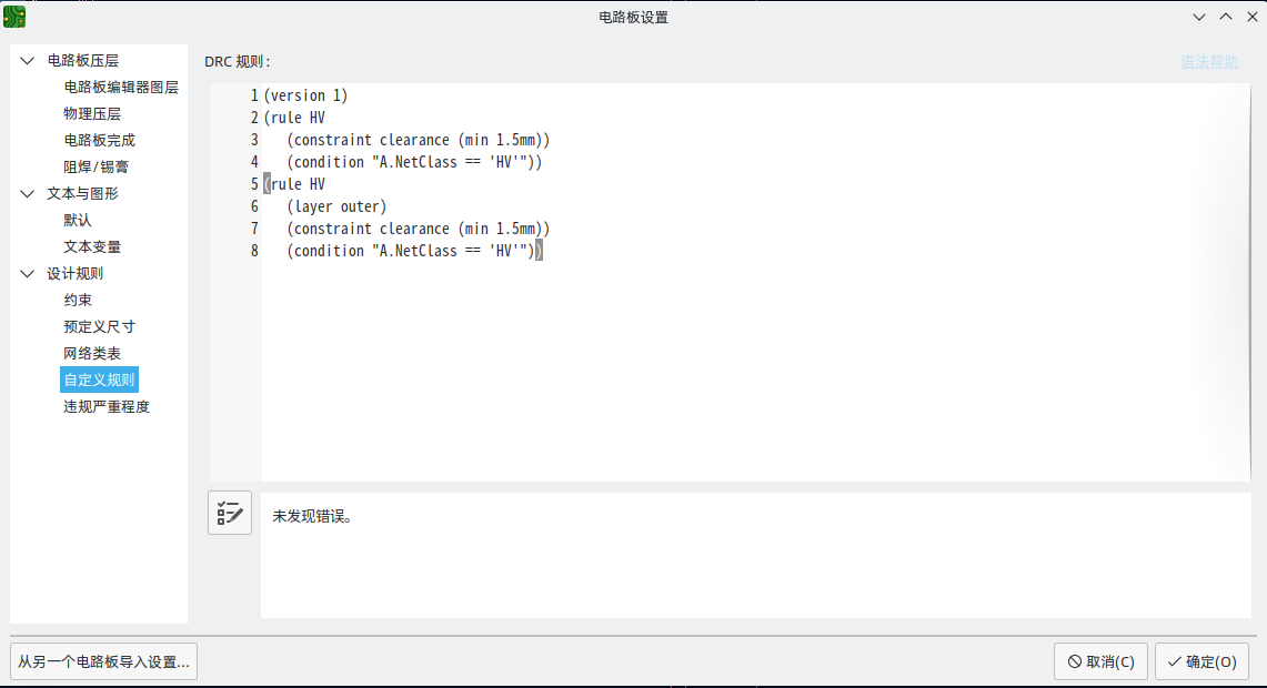
(rule "Power component clearance"
    (condition "A.hasComponentClass('Power_Stage')")
    (constraint clearance (min 0.3mm))
)
To enforce courtyard clearance between two component classes:
(rule "Keep analog away from digital"
    (condition "A.hasComponentClass('Analog') && B.hasComponentClass('Digital')")
    (constraint courtyard_clearance (min 2mm))
)
See Custom Design Rules for the full expression language reference and additional examples.
Custom rules
自定义规则部分包含一个文本编辑器,用于使用自定义规则语言创建设计规则。 自定义规则用于创建基本约束或网络类设置没有涵盖的特定设计规则检查。
只有在自定义规则定义中没有错误时,才会应用自定义规则。 在关闭电路板设置之前,使用检查规则语法器按钮来测试定义并修复任何问题。
See Custom Design Rules in the Advanced Topics chapter for more information on the custom rules language as well as example rules.
Violation severity
违规严重性部分允许你配置每种设计规则检查的严重性。 每条规则可以被设置为创建一个错误标记、一个警告标记或没有标记(忽略)。
| 在设计规则检查器中可能会忽略个别规则违规。 在违规程度部分中将规则设置为忽略将完全禁用相应的设计规则检查。 请谨慎使用此设置。 |
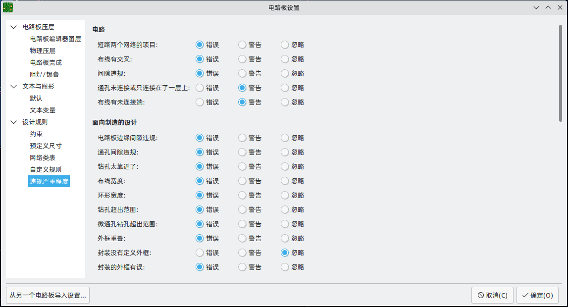
For descriptions of each violation type, and how to ignore individual violations without disabling all violations of that type, see the DRC documentation.
Embedding files
External files can be embedded within a board file. Embedding a file stores a copy of the file inside the board file. The design can then refer to the embedded copy of the file instead of the external file, which makes the project more portable as it doesn’t rely on an external file. Fonts, datasheets, drawing sheets, SPICE models, and footprint 3D models can be embedded and used within KiCad. Other arbitrary files can also be embedded to store them in the project for later export, but they are not used by any KiCad functionality. Files embedded in a board necessarily increase the board’s file size, although files are compressed before being embedded to minimize the space required.
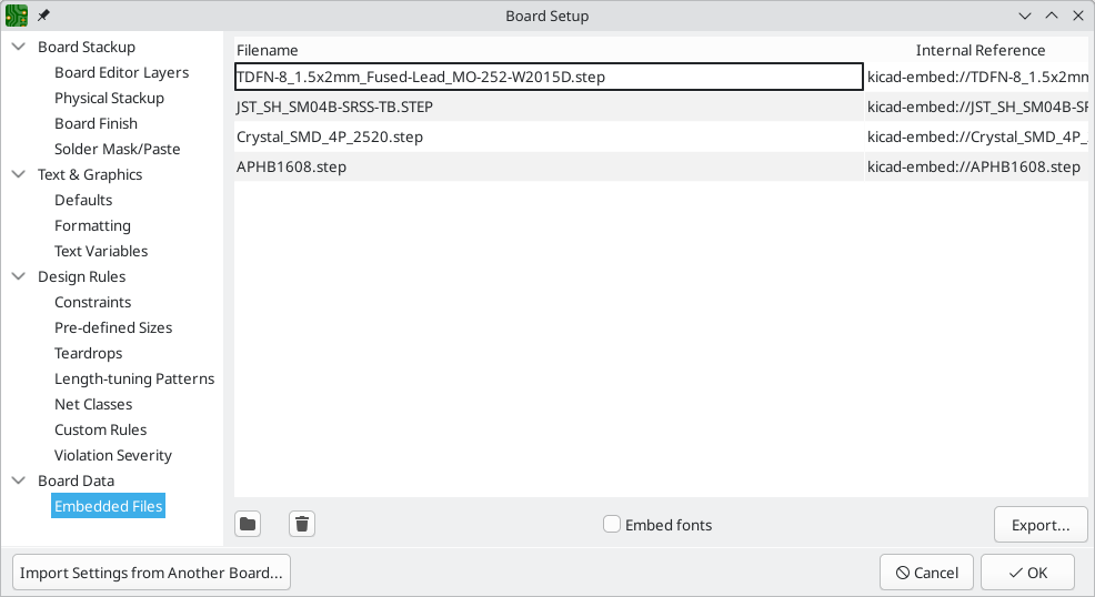
Embedded files are managed in the Embedded Files section of Board Setup. All files embedded in a board are shown here. To embed a file inside a board, click the ![]() button and select the file. The file is then embedded inside the PCB and is listed in the embedded files list along with its embedded reference. The embedded reference is a unique identifier for the embedded file that begins with
button and select the file. The file is then embedded inside the PCB and is listed in the embedded files list along with its embedded reference. The embedded reference is a unique identifier for the embedded file that begins with kicad-embed://. You can use the embedded reference elsewhere in the Board Editor to refer to the embedded file as if it were an external file path. You can copy the embedded reference by right clicking and selecting Copy Embedded Reference. To remove an embedded file, click the ![]() button. Any remaining links to the removed file will become invalid.
button. Any remaining links to the removed file will become invalid.
| 3D models and drawing sheets can be embedded directly using the file browser when you add them to a footprint (3D models) or to a board (drawing sheets) by enabling the Embed Files option in the file browser. This is a single-step shortcut for adding the files in Board Setup and then referring to them by their embedded reference; the result is the same. |
To embed any fonts used in a board, check the Embed fonts checkbox. All fonts used in the board design will be embedded, so text using that font can be edited on any computer regardless of whether the font file is installed.
You can also embed files in a footprint, either in the board copy of a footprint or in a library. Such files will be available within the footprint instance but not within the larger board design or within other footprints. Files embedded in a footprint are deduplicated when the footprint is added to a board: if a file is embedded in a footprint, and multiple instances of that footprint are added to the board, only one copy of the file will be embedded, and all of the footprint instances will refer to the same embedded file.
As an example, to embed a 3D model in a project and use it within several footprints, you could embed the model using the Board Setup dialog, copy the internal reference, and paste the internal reference as a 3D model path in each footprint that uses that model. Alternatively, you could embed the model within a single footprint, either in the board or in the source footprint library. In this case, the footprint itself is portable if you export the footprints from the board, and the model embedding is managed in the footprint’s properties rather than Board Setup. A more convenient way to achieve the same thing, however, is to open the footprint’s properties dialog, add a 3D model file, and enable the Embed File option in the file browser. Again, this could be done for a footprint in the board or for a footprint in the source footprint library.
| You can embed all of your board’s footprints at once using Tools → Collect and Embed 3D Models. This takes every external 3D model referenced by the board’s footprints and embeds the models in the board. The 3D model references in each footprint are replaced by references to the corresponding embedded files. |
Files can also be embedded in schematics.
导入设置
您可以从现有电路板导入部分或全部电路板设置。 这种技术可以用来创建一个 "模板" 电路板板,其中有你想在多个设计中使用的设置,然后将这些设置从模板板中导入到每个新板中,而不是手动输入。
| If you are frequently importing settings from a specific board, consider making a template project from that design. |
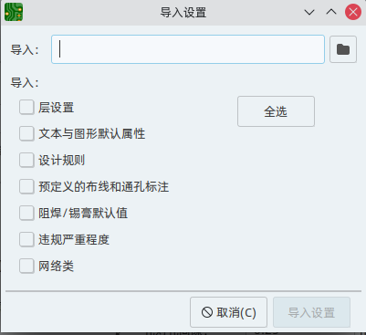
To import settings, click the Import Settings from Another Board… button at the bottom of the Board Setup dialog and then choose the kicad_pcb file you want to import from. Select which settings you want to import and the current settings will be overwritten with the values from the chosen board.
The settings that are available to import are:
-
Board layers and physical stackup
-
Solder mask/paste defaults
-
Zone hatched fill offsets
-
Text and graphics default properties
-
Text & graphics formatting
-
Design rule constraints
-
Predefined track & via dimensions
-
Teardrop defaults
-
Length-tuning pattern defaults
-
Net classes
-
Component classes
-
Tuning Profiles
-
Custom rules
-
Violation severities
编辑电路板
放置和绘制操作
放置和绘图工具位于右侧工具栏中。 当一个工具被激活时,它将一直处于激活状态,直到选择了一个不同的工具或用 Esc 键取消该工具。 当任何其他工具被取消时,选择工具总是被激活。
某些工具栏按钮在调色板中有多个可用工具。这些工具由按钮右下角的小箭头表示:
要显示调色板,你可以在工具上点击并按住鼠标按钮,或者点击并拖动鼠标。 调色板关闭时将显示最近使用的工具。
The default contents of the right toolbar are shown below.
| You can edit the toolbar’s contents in the Toolbar page of the PCB Editor Preferences. |
|
Selection tool (the default tool). When the rectangular selection mode is active, clicking and dragging performs a rectangular selection. When the lasso selection mode is active, clicking and dragging performs a lasso selection. Only one selection mode is visible in the toolbar at a time; you can expand the palette to choose another tool by clicking and holding/dragging. |
|
Local ratsnest tool: when the board ratsnest is hidden, selecting footprints with this tool will show the ratsnest for the selected footprint only. Selecting the same footprint again will hide its ratsnest. The local ratsnest setting for each footprint will remain in effect even after the local ratsnest tool is no longer active. |
|
Footprint placement tool: click on the board to open the footprint chooser, then click again after choosing a footprint to confirm its location. |
|
Route tracks / route differential pairs: These tools activate the interactive router and allow placing tracks and vias. The interactive router is described in more detail in the Routing Tracks section. Only one router type is visible in the toolbar at a time; you can expand the palette to choose another tool by clicking and holding/dragging. |
|
Tune length: These tools allow you to tune the length of single tracks or the length or skew of differential pairs, after they have been routed. Only one tuner type is visible in the toolbar at a time; you can expand the palette to choose another tool by clicking and holding/dragging. |
|
Add vias: place a standalone ("free") via without routing tracks. |
|
Add filled zone: Click to set the start point of a zone, then configure its properties before drawing the rest of the zone outline. Zone properties are described in more detail below. |
|
Add rule area: Rule areas, formerly known as keepouts, can restrict item placement and zone fills. You can also define named areas and apply specific custom DRC rules to them. |
|
Note: Lines are graphical objects and are not the same as tracks placed with the Route Tracks tool. |
|
Draw arcs: pick the center point of the arc, then the start and end points. By right clicking this button, you can change the arc editing mode between several editing modes that control how the arc center, endpoints, angle, and radius are maintained while the arc is edited. |
|
Draw rectangles. Rectangles can be filled or outlines. |
|
Draw circles. Circles can be filled or outlines. |
|
Draw graphical polygons. Polygons can be filled or outlined. Note: Filled graphical polygons are not the same as filled zones: graphical polygons cannot be assigned to a net and will not keep clearance from other items. |
|
Draw bezier curves. Each click alternates between fixing a curve node and fixing the control handle for the node that was just placed. |
|
Add bitmap image for reference. Reference images are not included in fabrication outputs. |
|
|
|
|
|
|
|
Add dimensions. Only one dimension type is visible in the toolbar at a time; you can expand the palette to choose another tool by clicking and holding/dragging. |
|
|
|
Deletion tool: click objects to delete them. |
|
Set grid origin or drill/place origin (used for fabrication outputs). Only one origin type is visible in the toolbar at a time; you can expand the palette to choose another tool by clicking and holding/dragging. |
|
Add a point. Points are nonphysical, dimensionless objects that can be used for snapping and documentation. |
|
Interactively measure the distance between two locations. |
Grids and snapping
When moving, dragging, and drawing board elements, you can make these operations snap to a grid or to snapping points on pads and other items. In complex designs, snap points can be so close together that it makes the current tool action difficult. Both grid and object snapping can be disabled while moving the mouse by using the modifier keys in the table below.
| On Apple keyboards, use the Cmd key instead of Ctrl. |
| Modifier Key | Effect |
|---|---|
Ctrl |
Disable grid snapping. |
Shift |
Disable object snapping. |
Tools only snap to objects on visible layers. You can reduce unwanted snapping points by hiding unneeded layers or using the single-layer view mode. Additionally, you can toggle between snapping to objects on all layers or only snapping to objects on the current layer by pressing Shift+S.
Snapping to different types of objects (pads, tracks, and graphics) can be configured in the Editing Options section of the PCB Editor preferences.
Snapping to graphical shapes
When working with graphic shapes like rectangles or arcs, such as when drawing shapes or when selecting a reference point for a move operation, many additional snapping points are available that let you snap to features of existing graphic shapes.
Available snapping points for graphic shapes include:
-
Endpoints and corners
-
Midpoints
-
Centers
-
Intersection points
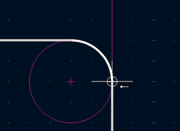
When you hover over a snap point with a shape tool active, a graphical icon will be shown that indicates a snapping point is active and explains the type of snapping point. Clicking will use that snapping point. Some shapes display auxiliary snapping lines that appear when you snap to part of that object. For example, line segments display an auxiliary line that continues the segment beyond its endpoint, and arcs display an auxiliary circle that completes the arc’s circumference. Auxiliary shapes can be used for snapping just like the original shape. An auxiliary line and circle are shown as a solid purple line in the screenshot below. The cursor indicates that the active snapping point is the endpoint of a line.
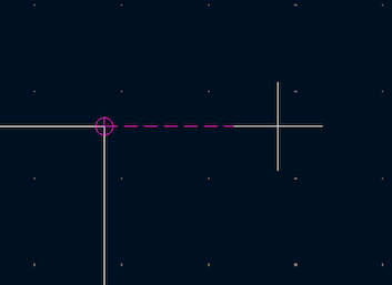
If you move the cursor away from the snapping point, a horizontal or vertical dashed line will appear, depending on the direction of motion. This indicates a horizontal or vertical projection from the snapping point, respectively. Following the line will maintain a position that is horizontally or vertically aligned to the original snap point. This projection is shown as a purple dashed line in the screenshot below.
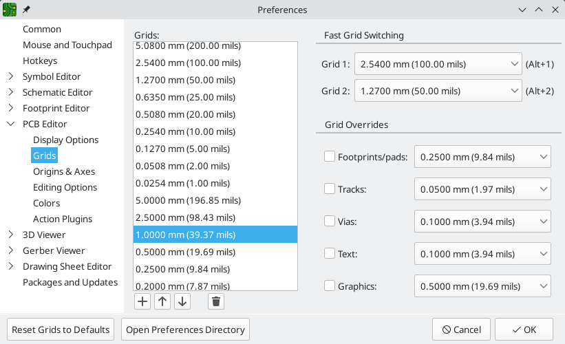
Grid settings
Interactive editing operations are snapped to the active grid. You can adjust the grid size using the grid dropdown in the top toolbar or by right-clicking and selecting a new grid from the list in the Grid submenu. Pressing the n or N hotkeys will cycle to the next and previous grid in the list, respectively.
You can also select a new grid or edit the available grids in the Grids pane of the preferences dialog. As a shortcut to reach this dialog, right click the ![]() button on the left toolbar and select Edit Grids….
button on the left toolbar and select Edit Grids….
In this dialog you can select an active grid from the list of grids, reorder the list of grids (![]() /
/ ![]() ), and add (
), and add (![]() ), remove (
), remove (![]() ), or edit (
), or edit (![]() ) grids. Grids defined in this dialog can have unequal X and Y spacing as well as an optional name. The grid spacing and name are specified when you create or edit a grid.
) grids. Grids defined in this dialog can have unequal X and Y spacing as well as an optional name. The grid spacing and name are specified when you create or edit a grid.
This dialog also lets you designate two grids from the list as "Fast Grids", which can be quickly selected using Alt+1 and Alt+2.
Finally, you can configure grid overrides for different types of objects. Grid overrides let you set particular grid sizes for different types of objects which will be used instead of the default grid when working with those objects. For example, you can set a 100 mil grid for footprints and pads while using smaller grids to finely position tracks, vias, and text. Grid overrides can be individually enabled and disabled in this dialog, or globally enabled and disabled using the ![]() button on the left toolbar (Ctrl+Shift+G).
button on the left toolbar (Ctrl+Shift+G).
To change the origin (zero point) of the grid, use Place → Grid Origin and click to place the origin in the canvas. This function is also available with the ![]() button in the right toolbar. Alternatively, you can enter explicit coordinates for the grid origin with Edit → Grid Origin….
button in the right toolbar. Alternatively, you can enter explicit coordinates for the grid origin with Edit → Grid Origin….
| The grid origin is one of several different origins in KiCad, which aren’t necessarily set to the same point. The grid origin is the point that the grid aligns to; shifting the grid origin also shifts every grid point. The page origin is an absolute origin which is always the top left corner of the drawing sheet. The drill/place file origin is a configurable point that can be used for fabrication outputs (Place → Drill/Place File Origin). Finally, the local origin is a quickly settable relative origin that current cursor location by pressing Space; the cursor coordinates relative to the local origin are displayed in the status bar. |
The visual appearance of the grid can also be customized in several ways. You can change the thickness of the grid markings, switch their shape (dots, lines, or crosses), and set the minimum displayed spacing in the Display Options page of the preferences dialog, and you can change the grid color in the Colors page of the preferences dialog.
The grid can be shown or hidden using the ![]() button on the left-hand toolbar. By default the grid is still active even if it is hidden, but this is configurable in the Display Options preferences page. There you can set the grid to be disabled when it is hidden or even disable the grid entirely.
button on the left-hand toolbar. By default the grid is still active even if it is hidden, but this is configurable in the Display Options preferences page. There you can set the grid to be disabled when it is hidden or even disable the grid entirely.
编辑对象属性
All objects have properties that are editable in a dialog. Use the hotkey E or select Properties from the right-click context menu to edit the properties of selected item(s). You can only open the properties dialog if all the items you have selected are of the same type. For many object types, like footprints, you can only edit the properties of a single item at one time. To edit the properties of multiple items at once, including items with different types, you can use the Properties Manager.
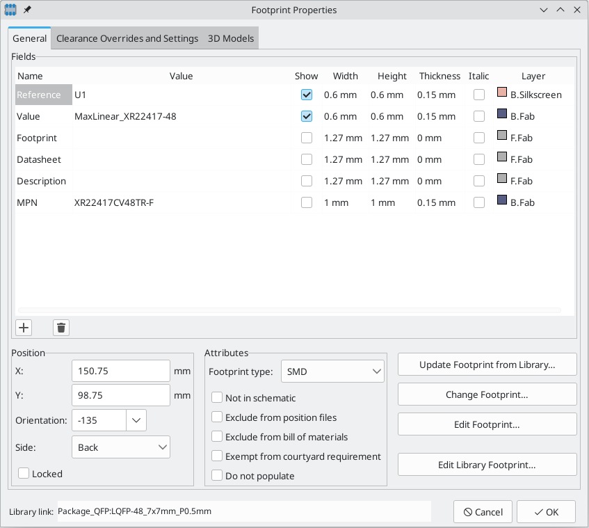
You can also view and edit item properties using the Properties Manager. The Properties Manager is a docked panel that displays the properties of the selected item or items for editing. If multiple types of items are selected at once, the properties panel displays only the properties shared by all of the selected item types.
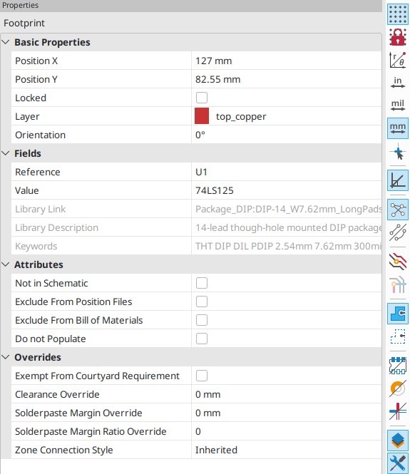
Editing a property in the Properties Manager immediately applies the change. When multiple items are selected, property modifications are applied to each selected item individually, not to the whole selection as a group. For example, when changing the orientation of multiple items, each item is individually rotated around its own origin, not the group’s origin.
Show the Properties Manager with View → Panels → Properties or the ![]() button on the left toolbar.
button on the left toolbar.
Several tools are available for editing properties of specific types of objects in bulk. For text and graphical items, including footprint fields and dimensions, you can use the Edit Text and Graphics Properties tool. Tracks and vias can be bulk-edited using the Edit Track and Via Properties tool. Teardrop properties can be edited with the Edit Teardrops tool.
In properties dialogs and many other dialogs, any field that contains a numeric value can also accept a basic math expression that results in a numeric value.
For example, a dimension may be entered as 2 * 2mm, resulting in a value of 4mm. Basic arithmetic operators as well as parentheses for defining order of operations are supported. Units can also be specified, and unit conversions are performed automatically, so 1in + 1mm evaluates to 26.4mm.
电路板边框 (Edge Cuts)
KiCad 使用 Edge.Cuts 层上的图形对象来定义电路板的边框。 边框必须是一个连续(封闭)的形状,但可以由不同类型的图形对象组成,如直线和弧,或者是一个单一的对象,如矩形或多边形。 如果没有定义电路板的边框,或者电路板的边框无效,那么一些功能,如 3D 查看器和一些设计规则的检查将无法发挥作用。
KiCad displays closed board outlines with a shaded interior, which is called the board area shadow. The shadow is only drawn for closed outlines, so you can use the shadow to check that the board outline is properly closed. It also indicates which regions are solid, as opposed to cutouts. You can adjust the color of the board area shadow, or hide it entirely, in the Objects tab of the Appearance panel.
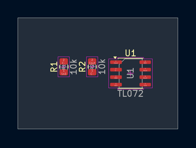
For the board outline to be considered valid, the endpoints of any shapes in the outline must coincide exactly. If any endpoints are not coincident with another endpoint, the outline will not be considered closed. Outline shapes also cannot intersect each other or overlap. In such cases, DRC will report a "Board has malformed outline" violation that points to the problematic parts of the outline.
| You can use the grid or the snapping tools to ensure outline endpoints exactly coincide. The Heal Shapes tool can also be used to fix small gaps between endpoints. |
If there are multiple closed shapes on the Edge.Cuts layer, each shape acts as an independent board outline. When an outline shape completely encloses another outline, the outermost shape is considered the outside edge of the board. Any closed shapes inside the outer shape are considered interior cutouts in the board. Each closed outline cannot intersect or overlap with other outlines.
Zones only fill when they are within the board outline. Any portion of a zone that is outside of the board outline, including inside an interior cutout, will not be filled.
使用封装
Adding footprints to the board
Footprints are automatically added to the board when the PCB is updated from the schematic. The footprint associated with each schematic symbol is added to the board if it is not already present, and each footprint pad is associated with the corresponding symbol pin’s net. Symbol pins are matched to footprint pads by pin/pad number.
When footprints are added to the board after an update from the schematic, they are clustered by schematic sheet and by geographical location in the schematic. They are initially attached to the cursor; you can place them by clicking in the desired location.
You can also add footprints to the board manually using the Add Footprint tool (A or the ![]() button).
button).
| Footprints added in this way will not be automatically associated with a symbol or have nets assigned to their pads, and subsequent updates from the schematic will remove these unassociated footprints unless the footprint is locked or the Delete footprints with no symbols option is unchecked in the Update PCB From Schematic dialog. For these reasons, it is usually recommended to avoid manually adding footprints to the board. Manually adding footprints is necessary for PCB-only workflows, and can also be useful for adding logos or other footprints that do not need a corresponding schematic symbol. |
Placing and moving footprints
Once footprints have been added to the board, you can reposition them in many ways.
The Move command (M) moves a footprint or a selection of footprints, ignoring any connected track segments that are not selected. No DRC checking is done when moving footprints with the Move command, although any footprint courtyards that collide with the moved footprint’s courtyard will be highlighted.
There is a reference point for the move operation, which is the point in the footprint which attaches to the cursor and therefore the point in the footprint that snaps to the grid and to other objects. The reference point during a move is determined by the location of the cursor when the Move command is initiated. If the cursor is over a pad, the pad’s center will be used as the reference point. If the cursor is not over a pad, the footprint’s anchor (coordinate origin point) will be used. To select an arbitrary snapping point, you can use the Move With Reference command instead of the regular Move command (right click → Move with Reference). After initiating the command, click on the desired reference point; KiCad will then begin the move with that point as the reference.
You can also use the Drag command (D) to move the selected footprint using the interactive router, maintaining all track connections to the footprint. Dragging footprints behaves like the Highlight Collisions router mode: obstacles will not be avoided or shoved, only highlighted. Ordinarily the router will prevent you from dragging a footprint into a position that violates DRC: when you click to commit a drag in a position that violates DRC, the footprint will return to its original position. To force a drag to be committed even if it violates DRC, Ctrl-click to commit the drag. Like the Move command, colliding courtyards are highlighted.
| Only tracks that end at the origin of the footprint’s pads will be dragged. Tracks that simply pass through the pad or that end on the pad at a location other than the origin will not be dragged. |
You can move a footprint to the opposite side of the board with the Flip command (F). Any parts of the footprint on a front layer will be swapped to the corresponding back layer, and vice versa.
Footprints can be rotated counter-clockwise using the R hotkey, or clockwise using Shift+R. By default, footprints are rotated by 90 degrees every time the rotate command is used, but you can configure the rotation angle step in Preferences → PCB Editor → Editing Options.
You can directly set a footprint’s exact absolute position, rotation angle, and PCB side using either the Footprint Properties dialog or the Properties panel.
To reposition a footprint relative to its current position, use the Move Exactly tool (Shift+M or right click → Position → Move Exactly…). The dialog lets you specify an X and Y translation, as well as a rotation, that will be applied to the footprint. The rotation can be performed relative to either the footprint’s anchor, the local coordinate origin, or the drill/place origin. You can also use polar coordinates instead of Cartesian coordinates.
To position a footprint relative to another object, you can use the Position Relative tool (Shift+P or right click → Position → Position Relative To…). With this tool, you select a reference point for the move and specify an offset. The footprint is moved to the specified offset relative to the reference point. The reference point can be one of the following:
-
The local origin, which is set to the cursor position when you press Space.
-
The grid origin, which is configured in the Grids dialog.
-
The location of an arbitrary item on the board, such as a specific pad in a footprint. After clicking the Select Item… button, click on the desired board item in the canvas to set the reference point.
-
An arbitrary point in the canvas. After clicking the Select Point… button, click at the desired location to set the reference point. You can use object snapping to select a specific point in an object, such as the end of a graphic line.
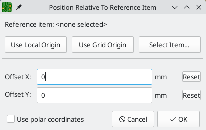
To position a footprint such that an arbitrary point in the footprint is positioned a certain distance from another arbitrary reference point, you can use the Interactive Offset tool (right click a footprint → Position → Interactive Offset Tool…).
This tool lets you interactively select two points that form the start and end of a position vector. The first point is a reference point in the footprint, and will move along with the footprint. The second point is a fixed reference that will remain stationary when the footprint is moved. The vector from the first point to the second point is shown graphically in the editing canvas. You can then give new X and Y (or polar) dimensions for the vector, which will move the footprint reference relative to the fixed reference such that the fixed reference is the specified distance from the footprint reference point. The dialog initially contains the vector dimensions before any move is performed, or in other words the initial distance between the footprint reference point to the fixed reference.
You can swap the position of two selected footprints using the Swap command (Alt+S). The first footprint is assigned the location, rotation, and board side of the second footprint, and vice versa. If there are more than two footprints selected, the locations are cycled: the last footprint gets the position of the first footprint, the first footprint gets the location of the second, and so on.
There are several convenience features that make it easier to find, select, and move specific footprints or footprints related to another footprint.
The Get and Move Footprint command (T) prompts you to choose a footprint from a list or by typing a reference designator. KiCad then attaches the chosen footprint to your cursor for a move operation.
There are two commands to select other footprints that need to be connected to the selected footprint but don’t yet have routed connections. The Select All Unconnected Footprints command (O) selects all footprints that have ratsnest lines to the currently selected footprints. The command can be executed repeatedly to further expand the selection based on the newly selected items. The Grab Nearest Unconnected Footprint command (Shift+O) selects the closest footprint with ratsnest lines to the currently selected footprint, and additionally begins to move it. If there are multiple footprints initially selected, the command will act like the Move Individually command described below, individually moving the closest unconnected footprint for each of the initially selected footprints.
You can select footprints based on their schematic sheet using the right click → Select → Items in Same Hierarchical Sheet command, which selects all other footprints that are in the same schematic sheet as the originally selected footprint.
If you want to move multiple selected footprints in sequence, use the Move Individually command (Ctrl+M). After triggering the command, KiCad will begin moving the first selected footprint. After you click to place the footprint, KiCad will immediately start moving the next footprint, in the same order that you selected the footprints. You can skip moving a footprint by pressing Tab, commit the current move and skip any remaining moves by double-clicking, or cancel all moves (including those already completed) by pressing Esc.
If you want to move a collection of footprints at once into one area, the Pack and Move Footprints command (P) closely packs the selected footprints together and moves them as a block.
| Move Individually and Pack and Move Footprints are useful in combination with other selection convenience features, such as cross-selection from the schematic or the advanced footprint selection features described above. For example, you could select a group of bypass capacitors in the Schematic Editor, switch to the PCB Editor where the corresponding footprints are now selected, and then use Move Individually to quickly place all of the bypass capacitor footprints close to their respective ICs. Alternatively, you could use one of the other selection tools, such as Select All Unconnected Footprints, to select many footprints from all over the board, then use Pack and Move Footprints to quickly put them all into a small area. |
Finally, KiCad can automatically place footprints onto the board. The auto-place function attempts to optimally place footprints to simplify ratsnest connections to other footprints. You can auto-place the selected footprints with Place → Auto-Place Footprints → Place Selected Footprints, or auto-place all footprints outside of the board outline with Place → Auto-Place Footprints → Place Off-Board Footprints.
Editing Footprints
Footprints in the board can be individually edited, both in terms of their properties (fields, attributes, clearance settings, etc.) and in terms of their physical pads and graphics. Editing a footprint in the board only affects that particular instance of the footprint; it does not affect any other copies of that footprint in the board, and it does not affect the library footprint.
To edit the properties of a footprint in the board, open its properties dialog (E)
The majority of the settings in this dialog are the same as in the footprint editor. You can edit the footprint’s fields, attributes, clearance and zone connection settings, 3D models, and embedded files, as in the footprint editor. However, here you can also set the footprint’s position, orientation, and side. You can also update the footprint from the library, exchange it for a different footprint, or edit the footprint itself in the footprint editor.
To edit the footprint’s physical form, i.e. its pads and graphics, you need to use the footprint editor. There are two buttons for opening a footprint in the editor, depending on whether you want to edit a single copy of a footprint in the board or a footprint’s source copy in the library.
-
Edit Footprint… will open the specific instance of the footprint in the footprint editor. Editing this footprint will only affect this one instance of the footprint in the board. It will not affect other instances of the footprint in the board, and it will not affect the library copy of the footprint. You can also open a board footprint in the footprint editor by right clicking the footprint in the board and selecting Open in footprint editor (Ctrl+E).
-
Edit Library Footprint… will open the library copy of the footprint in the footprint editor. Editing the library copy of the footprint will edit the footprint in the footprint library, but will not immediately affect any instances of that footprint in the board. To update footprints in the board with changes to the library footprint, use the Update Footprint from Library… tool. Editing the library footprint in this way is equivalent to opening the footprint editor, opening the appropriate footprint in its library, and editing it.
The Update Footprint from Library… button is used to update the board’s copy of the footprint to match the copy in the library. The Change Footprint… button is used to swap the current footprint to a different footprint in the library. These functions are described later.
Editing footprint fields
An individual symbol text field can be edited directly with the E hotkey (with a field selected instead of a footprint) or by double-clicking on the field.
The options in this dialog are the same as those in the full Footprint Properties dialog, but are specific to a single field.
Only footprint fields can be edited this way in the board editor. Unlike fields, Footprint text is a graphic object that can only be edited or moved in the footprint editor.
| In versions of KiCad before version 8.0, footprint fields did not exist. Instead, footprint text could be edited directly in the board editor. Since KiCad 8.0, footprint text is not editable in the board editor and can only be edited in the footprint editor. |
Updating and exchanging footprints
When a footprint is added to the board, KiCad embeds a copy of the library footprint in the board so that the board is independent of the system libraries. Footprints that have been added to the board are not automatically updated when the library changes. Library footprint changes are manually synced to the board so that the board does not change unexpectedly.
| You can use the Compare Footprint with Library tool to inspect the differences between a footprint in a board with its corresponding library footprint. |
To update footprints in the board to match the corresponding library footprint, use Tools → Update Footprints from Library…, or right click a footprint and select Update Footprint…. You can also access the tool from the footprint properties dialog.
The top of the dialog has options to choose which footprints will be updated. You can update all footprints on the board, update only the selected footprints, or update only the footprints that match a specific reference designator, value, or library identifier. The reference designator and value fields support wildcards: * matches any number of any characters, including none, and ? matches any single character.
The middle of the dialog has options to control what parts of the footprint will be updated. You can select specific fields to update or not update, which properties of the fields to update (text content, visibility, size and style, and position), and how to handle fields that are missing or empty in the library footprint. You can also choose whether to update clearance overrides and footprint attributes, such as footprint type, not in schematic, exclude from position files / bill of materials, exempt from courtyard requirement, and do not populate.
The bottom of the dialog displays messages describing the update actions that have been performed.
To change an existing footprint to a different footprint, use Edit → Change Footprints…, or right click an existing footprint and select Change Footprint…. This dialog is also accessible from the footprint properties dialog.
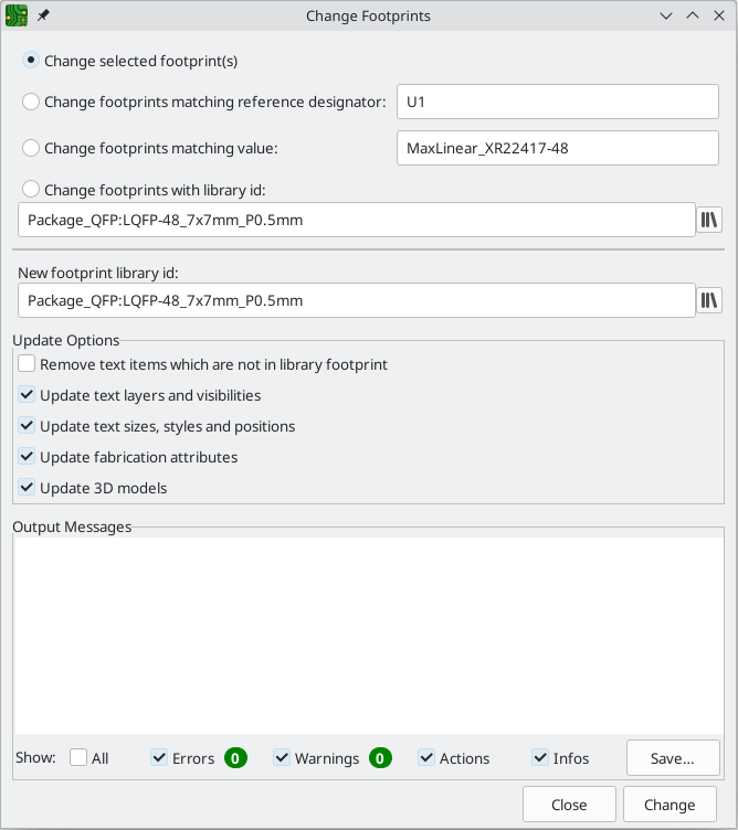
The options for the Change Footprints dialog are very similar to the Update Footprints from Library dialog.
Match pad positions
The Match pad positions option will automatically attempt to compensate for changes in the footprint origin and orientation in the library. This can happen, for example, if the library changes a part, or you switch to a library with different zero-orientation conventions.
When this option is off, the update process will not adjust the position of the new footprint. This may result in disconnected tracks if the library part has changed.
When this option is on, it will attempt to update the position and rotation for minimal impact on the layout. If a minority of pads have changes position, the footprint will be positioned so as to keep as many connections as possible untouched. If a majority of pads are moved, the footprint will be positioned so as to minimise the offsets on average.
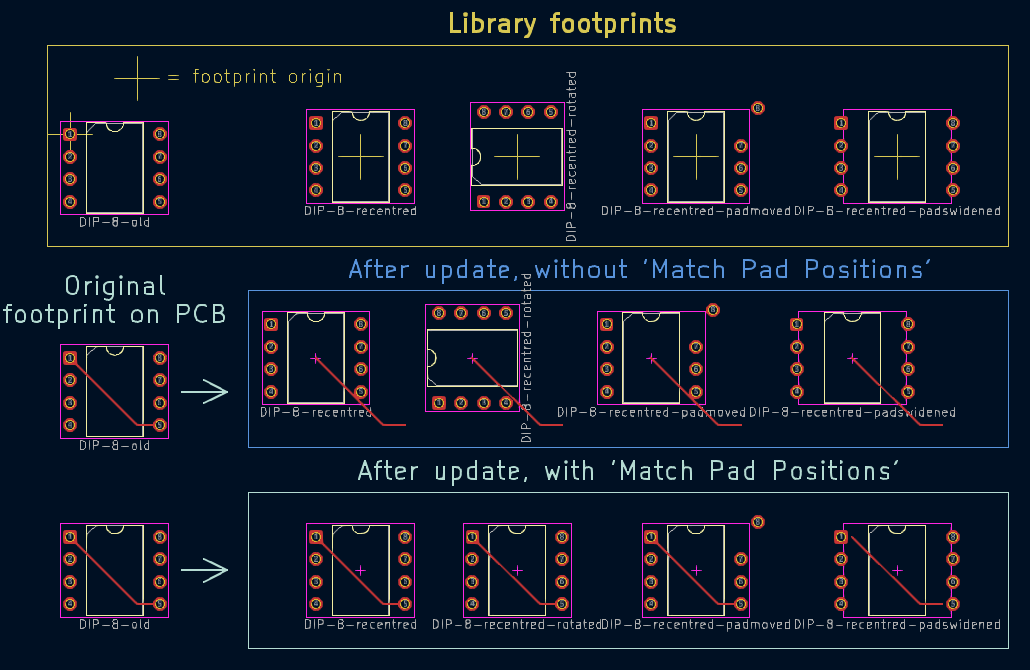
Comparing footprints between board and library
When a footprint in a board diverges from the corresponding footprint in the original footprint library, you can use the Compare Footprint with Library tool to inspect the differences between the two versions of the footprint. Run the tool using Inspect → Compare Footprint With Library.
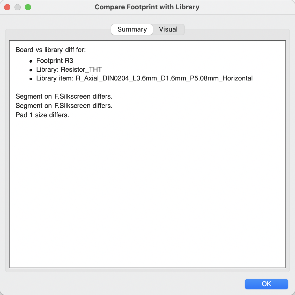
The Summary tab shows the name of the footprint, including its library and board reference designator, and provides a list of the differences between the board and library versions of the footprint.
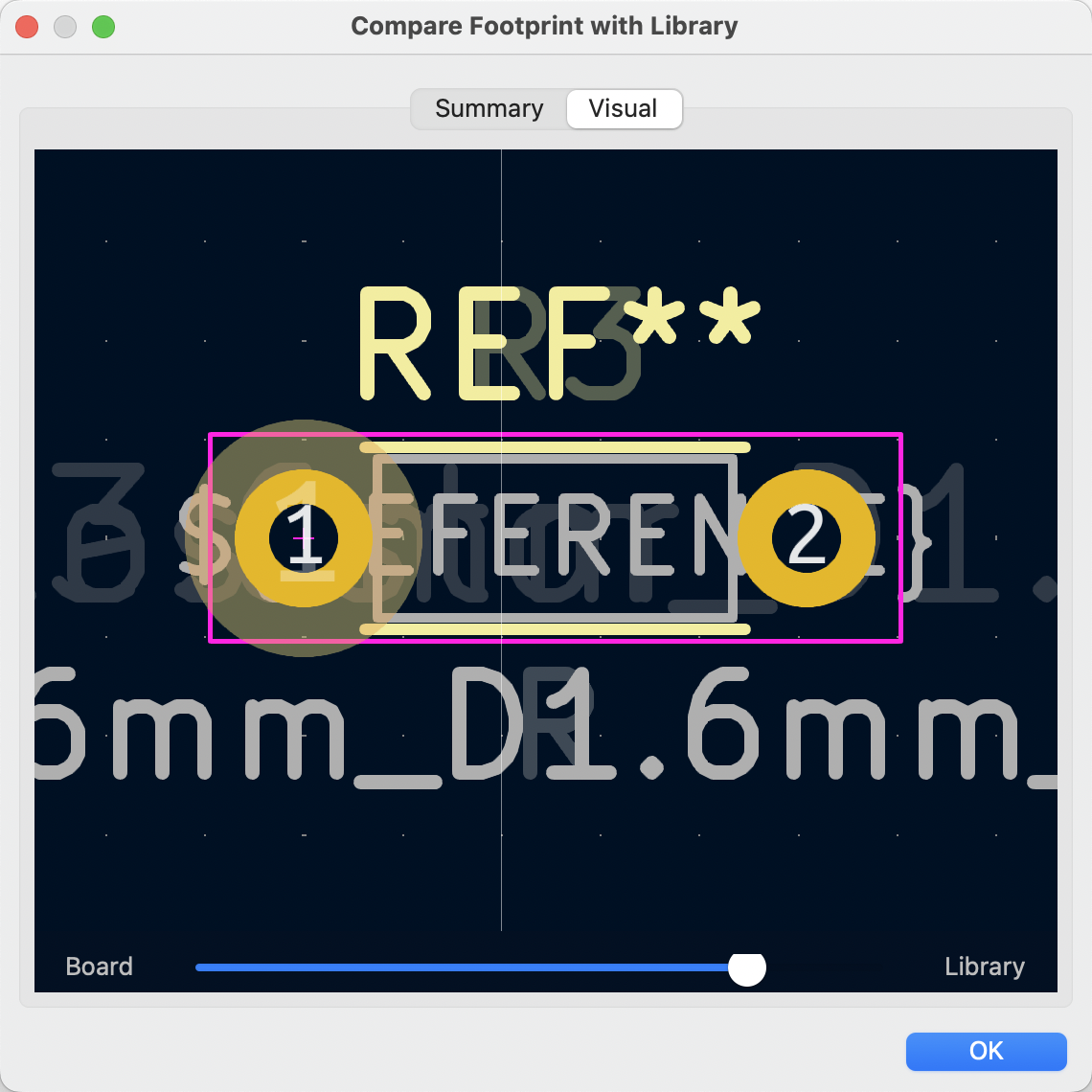
The Visual tab shows a visual comparison of the board and library versions of the footprint. This can be used as a visual diff tool.
By default, the comparison displays both versions of the footprint superimposed on each other. To see the changes more easily, you can drag the slider at the bottom of the tab to the right to emphasize the library version of the footprint in the superimposed view (making the board version of the footprint more transparent) or drag it to the left to emphasize the board version (making the library version more transparent). At the far right and left ends of the slider, the board and library versions of the footprint, respectively, are fully hidden. It may be helpful to drag the slider back and forth to see the changes more clearly.
You can press the A/B button, or use the / hotkey, to quickly toggle back and forth between the board and library versions.
The Update Footprint from Library… button opens the Update Footprint from Library tool to update the footprint to match the library.
The screenshot above shows a visual comparison with the board version of the footprint deemphasized. Looking at pad 1 on the left, you can see a large, partially transparent pad (from the board footprint) surrounding a fully opaque, smaller pad (from the library footprint). This indicates that the pad was enlarged in the board version of the footprint, or shrunk in the library version of the footprint.
使用焊盘
在将封装放置在电路板上之后,可以检查和编辑封装的每个单独的焊盘的属性。 换句话说,如果库中的封装设计不合适,就可以在电路板上封装的特定实例中覆盖单个封装焊盘的设计。 例如,你可能希望为一个需要在特定设计中保持不焊接的焊盘去除锡膏孔,或者你可能希望移动一个轴向引线电阻的通孔焊盘的位置,以适应特定的设计。
| 默认情况下,所有封装焊盘的位置都被锁定,因此可以编辑焊盘属性,但不能移动焊盘相对于封装其他部分的位置。 焊盘可以被解锁以允许自由移动,这对某些应用很有用(如具有不同引线位置的通孔封装),但通常不建议用于表面贴装封装。 |
当一个焊盘被选中时,焊盘属性对话框将通过上下文菜单或默认的快捷键 E 打开。 请注意,KiCad 认为如果你在焊盘附近点击,你可能是想选择整个封装而不是单个焊盘。 要选择单个焊盘,请确保在焊盘区域内点击,或者关闭选择过滤器中的 "封装" 设置(并确保 "焊盘" 设置打开),以防止意外地选择整个封装而不是特定的焊盘。
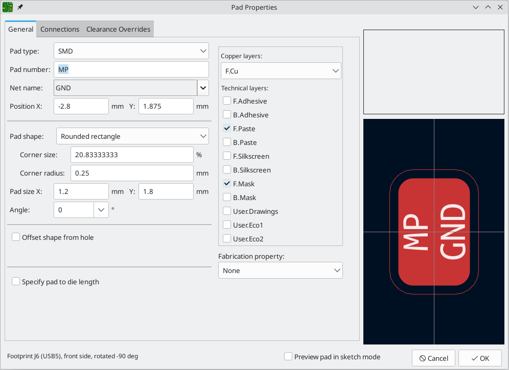
This dialog lets you edit the physical properties of the pad, including size and shape. You can also modify how the pad connects to other objects on the board, including clearance properties, teardrops, and thermal reliefs.
This dialog is the same as the pad properties dialog in the footprint editor, except that here you can also manually assign a net to a pad using the net name selector. The remaining options are explained in the Footprint Editor documentation.
| While you can manually assign nets to pads in the PCB editor, this is not a typical workflow. Usually net-to-pad connections are defined by the schematic and then transferred to the PCB editor. |
使用敷铜
敷铜区域,有时也被其他 EDA 工具称为铺铜或覆铜,是分配给一个特定网络的实心或网格状的铜箔区域,敷铜区域会自动保持与其他铜对象的间隙。 敷铜区域通常用于填充板层(或板层的一部分)上的所有自由空间,以创建接地和电源平面,承载大电流,或提供屏蔽。
| 一些 EDA 工具有单独的工具用于创建 "平面层" 及在信号层上创建敷铜区域。 在 KiCad 中,敷铜工具用于这两种应用。 |
Zones are defined by a polygonal outline that defines the maximum extent of the filled copper area. This outline does not represent physical copper and will not appear in exported manufacturing data. The actual copper areas of the zone must be filled each time the outline, or any objects inside the outline, are modified. Typically all zones in a board are filled at once (default hotkey B), but you can also run the filling process on individual zones (right click → Zones → Draft Fill Selected Zone(s)). Zones may be unfilled (default hotkey Ctrl+B) to improve performance and reduce visual clutter while editing large boards.
| By default, zone filling is a manual process rather than occurring every time an object changes that would result in a change to the zone copper. This is because zone filling can be a slow process on older computers or very large designs. It is important to make sure zone fills are up-to-date before generating outputs. KiCad will check that zones have been updated and warn you before generating outputs or running DRC when zones have not yet been refilled. You can optionally enable automatic zone-filling in the Preferences dialog (PCB Editor → Editing Options → Miscellaneous → Automatically refill zones). |
A zone fill occupies any unused space within the zone outline, automatically maintaining a specified clearance to board edges, holes, and copper objects on different nets. Zones do not fill outside of the board outline or within interior cutouts.
Each zone also has a priority. Zone priority determines the order in which multiple zones on a single layer are filled. The highest priority level zone on a given layer will be filled first. Lower-priority zones will keep clearance to the filled areas of higher-priority zones.
The main way to set zone priorities is by adjusting the relative ordering of zones in the Zone Manager dialog. Zones that are higher in the list have higher priority than zones lower in the list. As a shortcut, you can adjust a zone’s priority by right clicking it and choosing the appropriate action from the Zones → Zone Priority submenu. You can also directly set a zone’s priority by changing the Priority value in properties panel for the zone.
Drawing zones
To draw a zone, click the Add Filled Zone tool (![]() ) on the right toolbar, or use default hotkey Ctrl+Shift+Z. Click to choose the first point of the zone outline. The Zone Properties dialog will appear, allowing you to choose the zone net and other properties. These properties may be edited at any time, so it is not critical to choose them all correctly at first. Accept the dialog and continue placing points to define the zone outline. To finish the zone, double-click to set the last point.
) on the right toolbar, or use default hotkey Ctrl+Shift+Z. Click to choose the first point of the zone outline. The Zone Properties dialog will appear, allowing you to choose the zone net and other properties. These properties may be edited at any time, so it is not critical to choose them all correctly at first. Accept the dialog and continue placing points to define the zone outline. To finish the zone, double-click to set the last point.
| You can configure default properties for new zones on the Defaults page of Board Setup. |
To modify an existing zone outline, select it, then drag its editing handles to change the shape. Moving a handle at the corner of a zone will move that corner, displaying the angle of that corner and the two adjacent corners. Moving a handle on the edge of a zone will move that edge in a direction perpendicular to the edge. Normally, dragging an edge maintains the angles of the corners adjacent to the edge while allowing the edge’s length to vary. Holding Ctrl instead holds the edge’s length constant and allows the adjacent corner angles to vary.
To precisely position a corner, right click the corner’s handle and choose Shape Modification → Move Corner To…, then enter new X and Y coordinates for the corner. You can also edit the coordinates of every outline corner by right clicking the zone and choosing Shape Modification → Edit Corners…. This opens a floating dialog with a table containing the coordinates of every corner. Editing the coordinates of a corner immediately updates the zone outline.
| You can also create zones by converting an existing graphic shape to a zone. This can be useful, for example, for creating a zone with a shape that would otherwise be difficult to draw with the zone tool, such as a circle. To convert a shape to a zone, right click the shape, then select Create from Selection → Create Zone from Selection…. |
Several other tools for editing zones are available in the Zones submenu of the right click context menu. You can also add keyboard shortcuts to these actions in Preferences.
-
You can merge two zones by selecting both zones, right clicking, and choosing Zones → Merge Zones. When zones are merged, their outlines are combined into a single outline. The merged zone’s priority is taken from the highest priority of the zones you started with. In order to be merged, the zones must overlap, be on the same layers, and be assigned to the same net.
-
You can add a cutout to a zone by selecting the zone, right clicking, and choosing Zones → Add a Zone Cutout. You can then draw the outline of the cutout. When the zone is filled, the cutout region will remain unfilled.
-
To copy a zone an existing zone, you can right click a zone and choose Zones → Duplicate Zone onto Layer…. This creates a copy of the existing zone and allows you to change the new zone’s properties, including its layers.
| If you want to add a layer to an existing zone without changing any other properties, you can also achieve this by editing the existing zone’s properties and enabling the desired layer in addition to the existing layers. |
-
You can draw a new zone with the same settings as an existing zone by right clicking a zone and choosing Zones → Add a Similar Zone, then drawing the outline of the new zone. The new zone’s settings will be taken from the original zone.
Zone properties
To edit the zone’s properties, use hotkey E or select Properties from the context menu.
| In previous versions of KiCad, zone priority (the order in which multiple zones on a single layer are filled) was determined by a number assigned to each zone in the Zone Properties dialog. In KiCad 10 and later, zone priority is set by the relative ordering of zones in the Zone Manager. You can also set an explicit priority value for each zone in the properties panel. |
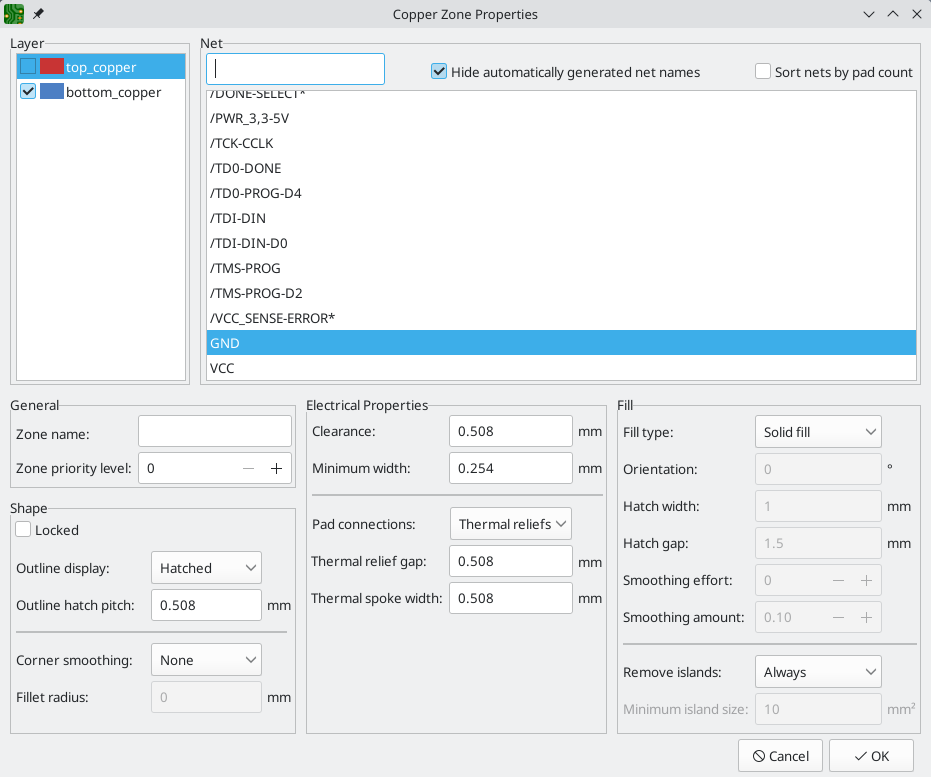
- Layers
-
A single zone object can create filled copper on one or more copper layers. Check the box next to each copper layer that this zone outline should fill on. The copper on each layer will be filled independently, but all layers will share the same net.
- Zone name
-
You can optionally assign a specific name to a zone. This name can be used to refer to the zone in custom DRC rules.
- Net name
-
Select the electrical net that the zone copper should be connected to. It is possible to create zones with no net assignment. Zones with no net will keep clearance from any copper objects on any net.
- Locked
-
Controls whether or not the zone outline object is locked. Locked objects may not be manipulated or moved, and cannot be selected unless the Locked Items option is enabled in the Selection Filter panel.
- Corner smoothing
-
Controls the behavior of the filled copper areas at corners of the outline. Corners can be smoothed by a chamfer or fillet, or can extend all the way to the outline corner if smoothing is disabled. The chamfer or fillet size is configurable when those modes are selected.
| By default, chamfers and fillets are not added to inside corners of the zone outline, because this would result in filled copper extending outside the outline. If smooth inside corners are desired, enable the Allow fillets outside zone outline option in the Constraints section of the Board Setup dialog. |
- Remove islands
-
Controls the behavior of isolated copper areas, also called islands, after the initial zone fill. When this is set to always, isolated areas inside the zone are removed. When set to never, isolated areas are left alone, and will result in copper areas that are not connected to the rest of the net. When set to below area limit, a minimum island size can be specified, and islands below this threshold will be removed.
| Regardless of the remove islands setting, islands are never removed from zones that are electrically unconnected. In other words, islands are only removed from zones that have at least one electrical connection. |
- Open Zone Manager…
-
Clicking this button opens the Zone Manager dialog. The Zone Manager can be used to view and edit all zones on the board, as well as configure zone priorities.
Clearances & pad connections
- Clearance
-
Controls the minimum clearance the filled areas of this zone will keep from other copper objects. Note that if two clearance values are in conflict, the larger clearance value will be used. For example, if a zone is set to use 0.2mm clearance but its netclass is set to use 0.3mm clearance, the result will be an 0.3mm clearance.
- Minimum width
-
Controls the minimum size of narrow necks of copper created inside the zone. Any copper areas that would be below this minimum width are removed during the filling process.
- Pad connection
-
Controls the way that the filled zone areas will connect to footprint pads on the same net. Solid connections will result in the copper completely overlapping the pads. Thermal reliefs will result in small copper spokes connecting the pad to the rest of the copper zone, increasing the thermal resistance between the pad and the rest of the zone. This can be useful for hand soldering. Reliefs for PTH will apply thermal reliefs to plated through-hole pads and use solid connections for surface mount pads. None will result in the zone not connecting to any pads on the same net.
- Thermal relief gap
-
Controls the distance maintained between any pad and the copper zone when the pad connection mode is set to generate thermal reliefs.
- Thermal spoke width
-
Controls the width of the "spokes", or short copper segments connecting the pad to the rest of the copper zone.
Display overrides
- Outline display
-
Controls how the zone outline is drawn on screen. In Line mode, only the border lines of the outline are drawn. In Hatched mode, hatch lines are drawn on the inside of the outline border for a short distance, to make the zone outline more apparent. In Fully Hatched mode, hatch lines are drawn across the entire inside of the zone outline.
- Outline hatch pitch
-
Controls the spacing between hatch lines in the Hatched and Fully Hatched outline display modes.
Hatched fill
- Hatched fill
-
When enabled, the zone is filled with a hatched pattern instead of solid copper. A hatched fill contains less copper than a solid fill. This can be useful for flexibile printed circuits and other specialty applications.
- Orientation
-
Controls the angle of the hatch pattern lines. An orientation of 0 degrees will result in the hatch pattern using horizontal and vertical lines.
- Hatch width
-
Controls the width of each line in the hatch pattern.
- Hatch gap
-
Controls the distance between each line in the hatch pattern.
- Smoothing effort
-
Controls the style of smoothing applied to the hatch pattern. A value of 0 will result in no smoothing, and a value of 3 will result in the finest smoothing. Higher values will result in longer processing time and larger Gerber files.
- Smoothing amount
-
A ratio that controls the size of the smoothing chamfers or fillets that are generated when smoothing effort is set to a value other than 0. An amount of 0.0 results in no smoothing, and a value of 1.0 results in maximum smoothing (in other words, a chamfer or fillet equal to half of the hatch gap).
- Hatch offset overrides
-
This table allows you to configure specific hatch pattern offsets for individual layers. X and Y offsets can be configured separately. Per-layer hatch offsets can be used to force the hatching grid to be offset from one layer to another, which is required in some applications.
| You can configure default hatch offsets for each layer in the Zone Hatch Offsets page of Board Setup. |
Zone manager
Instead of editing a single zone with the Zone Properties dialog, you can use the Zone Manager tool to you view, edit, and prioritize all zones in the board at once. To run the Zone Manager, click Tools → Zone Manager.
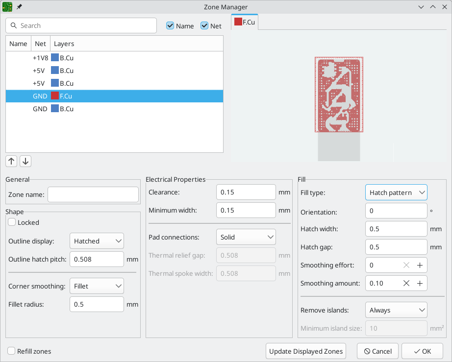
Zone list
The left side of the dialog shows a list of all zones in the board, displaying the name (if any), net, and layers for each zone.
The order of the zones in the list reflects the priority of each zone: higher priority zones are higher in the list. To change the priority of a zone, drag it to a new position in the list, or use the ![]() and
and ![]() buttons to move it up or down in the list. Use the
buttons to move it up or down in the list. Use the ![]() and
and ![]() buttons to move it to the very highest or lowest priority.
buttons to move it to the very highest or lowest priority.
To automatically assign a priority to each zone, press the ![]() button. This tool uses an algorithm to choose an appropriate priority for each zone. For each pair of zones that overlap each other, the tool assigns a higher priority to the zone with more connected pads or vias in the overlap region. If the two zones in the pair have approximately the same number of connected items in the overlapping region, the smaller zone gets a higher priority.
button. This tool uses an algorithm to choose an appropriate priority for each zone. For each pair of zones that overlap each other, the tool assigns a higher priority to the zone with more connected pads or vias in the overlap region. If the two zones in the pair have approximately the same number of connected items in the overlapping region, the smaller zone gets a higher priority.
You can filter the list of zones by typing into the filter box. The filter matches against the zones' name and/or net, depending on which filter options are enabled. You can also filter the list by zone layer using the Layer dropdown menu.
Zone preview
Selecting a zone in the list shows a preview of that zone in the bottom right. The preview can be zoomed and panned using the same controls as the PCB Editor canvas.
| You can reset the preview to show the entire zone by right clicking the preview and choosing Zoom to Fit. |
If the selected zone spans multiple layers, each layer is shown individually. You can preview each layer by clicking the appropriate layer tab above the preview.
Zone settings
The right side of the dialog shows the settings for the selected zone, which are explained above.
You can preview the new settings by clicking the Update Displayed Zones button, which updates the zone preview without affecting the board. Changing the properties of a zone in the Zone Manager will not update the board until you press OK.
If the Refill zones option is enabled, all zones will be refilled when you accept the dialog. If Refill zones is not enabled, zones will not be refilled until you manually refill them.
Routing tracks and vias
KiCad 具有交互式布线器的功能:
-
Allows manual or guided (semi-automatic) routing of single tracks and differential pairs
-
可通过以下方式修改现有设计:
-
拖动已有导线时进行重新布线
-
拖动封装时对连接到封装焊盘的导线进行重新布线
-
-
允许通过插入蛇形线
+来调整布线长度和差分对的偏移(相位) 为具有严格时序要求的设计调整布线形状
默认情况下,布线器在放置布线时遵循配置的设计规则:新布线的尺寸(宽度)将取自设计规则。在确定新布线和过孔的放置位置时,布线器将遵循设计规则中设置的铜间隙。 如果需要的话,可以通过使用高亮冲突布线器模式,或打开布线器设置中的 “允许 DRC 违规” 选项来禁用这种行为(见下文)。
The router has three modes that can be selected at any time in the Interactive Router Settings dialog. The router mode is used for routing new tracks, but also when dragging existing tracks using the Drag (hotkey D) command. These modes are:
-
Highlight Collisions: in this mode, most of the router features are disabled and routing is fully manual. When routing, collisions (clearance violations) will be highlighted in green and the newly-routed tracks cannot be fixed in place if there is a collision unless the Allow DRC Violations option is turned on. In this mode, up to two track segments may be placed at a time (for example, one horizontal and one diagonal segment).
-
Shove: in this mode, the track being routed will walk around obstacles that cannot be moved (for example, pads and locked tracks/vias) and shove obstacles that can be moved out of the way. The router prevents DRC violations in this mode: if there is no way to route to the cursor position that does not violate DRC, no new tracks will be created.
-
Walk Around: in this mode, the router behaves the same as in Shove mode, except no obstacles will be moved out of the way.
Which mode to use is a matter of preference. For most users, we recommend using Shove mode for the most efficient routing experience or Walk Around mode if you do not want the router to modify tracks that are not being routed. Note that Shove and Walk Around modes always create horizontal, vertical, and 45-degree (H/V/45) track segments. If you need to route tracks with angles other than H/V/45, you must use Highlight Collisions mode and enable the Free Angle Mode option in the Interactive Router Settings dialog.
There are four main routing functions: Route Single Track, Route Differential Pair, Tune length of a single track, and Tune skew of a differential pair. All of these are present in both the Route menu dropdown (individually) on the top toolbar and the drawing toolbar in two overloaded icons on the drawing toolbar on the right. The use of the overloaded icons is described above. One is for the two Route functions and one is for the two Tune functions. In addition, the Route menu allows the selection of Set Layer Pair and Interactive Router Settings.
要进行布线布线,请点击布线 ![]() 图标(从绘图工具栏或从顶部工具栏 布线 菜单中)或使用快捷键 X。 点击一个起始位置,选择要布线的网络,并开始布线。 布线的网络会自动高亮显示,网络允许的间隙会在当前布线的周围用灰色的轮廓表示。 可以通过改变 "偏好设置" 对话框中的 "间隙轮廓" 设置来禁用间隙轮廓功能。
图标(从绘图工具栏或从顶部工具栏 布线 菜单中)或使用快捷键 X。 点击一个起始位置,选择要布线的网络,并开始布线。 布线的网络会自动高亮显示,网络允许的间隙会在当前布线的周围用灰色的轮廓表示。 可以通过改变 "偏好设置" 对话框中的 "间隙轮廓" 设置来禁用间隙轮廓功能。
| The clearance outline shows the maximum clearance from the routed net to any other copper on the current layer. It is possible to use custom design rules to specify different clearances for a net to different objects. These clearances will be respected by the router, but only the largest clearance value will be shown visually. |
当布线器处于活动状态时,将从布线起点到编辑器光标绘制新的线段。这些线段是未固定的临时 (unfixed temporary) 对象,它们显示当您左键鼠标或 Enter 键来确定布线 (fix the route) 时将创建哪些线段。非固定布线段以比固定布线段更亮的颜色显示。当您使用 Esc 键或通过选择另一个工具退出布线器时,将只保存固定布线段。完成布线操作(快捷键 End) 将固定所有布线并退出布线器。
在布线时,可以使用 "撤消上一个布线段" 命令 (快捷键 Backspace) 取消上一个固定的布线。您可以重复使用此命令后退已固定的布线。
In previous versions of KiCad, using the left mouse button or Enter to fix the routed segments would fix all segments up to but not including the segment ending at the mouse cursor location. In KiCad 6 and later, this behavior is optional, and by default, all segments including the one ending at the mouse cursor location will be fixed. The old behavior can be restored by disabling the "Fix all segments on click" option in the Interactive Router Settings dialog.
布线时,可以按住 Ctrl 键禁用网格捕捉,按住 Shift 键禁用对焊盘和过孔等对象的捕捉。
| 也可以通过更改偏好设置对话框的编辑选项部分中的磁吸点首选项来禁用对象的捕捉。 我们建议您在一般情况下保持启用对象捕捉,这样就不会意外地在焊盘或过孔上略微偏离中心结束布线。 |
交互式布线设置
The interactive router settings can be accessed through the Route menu, or by right-clicking on the ![]() button in the toolbar. These settings control the router behavior when routing tracks as well as when dragging existing tracks.
button in the toolbar. These settings control the router behavior when routing tracks as well as when dragging existing tracks.
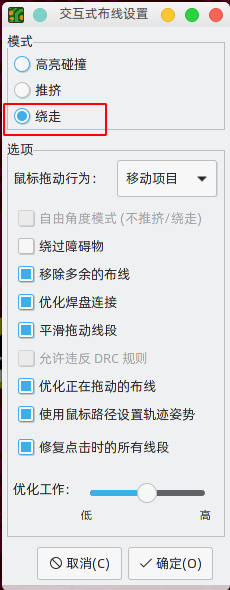
| Setting | Description |
|---|---|
Mode |
Sets the operating mode of the router for creating new tracks and dragging existing tracks. See the routing overview for more information. |
Free angle mode |
Allows routing tracks at any angle, instead of just at 45-degree increments. This option is only available if the router mode is set to Highlight collisions. |
Allow DRC violations |
Allow placing tracks and vias that violate DRC rules. This option is only available if the router mode is set to Highlight collisions. |
Shove vias |
Allow the router to shove vias along with tracks. When this is disabled, vias cannot be shoved. This option is only available if the router mode is set to Shove. |
Jump over obstacles |
Allow the router to attempt to move colliding tracks behind solid obstacles (such as pads). This option is only available if the router mode is set to Shove. |
Remove redundant tracks |
Automatically removes loops created in the currently-routed track, keeping only the most recently routed section of the loop. |
Optimize pad connections |
When this setting is enabled, the router attempts to avoid acute angles and other undesirable routing when exiting pads and vias. |
Smooth dragged segments |
When dragging tracks, attempts to combine track segments together to minimize direction changes. |
Optimize entire track being dragged |
When enabled, dragging a track segment will result in KiCad optimizing the rest of the track that is visible on the screen. The optimization process removes unnecessary corners, avoids acute angles, and generally tries to find the shortest path for the track. When disabled, no optimizations are performed to the track outside of the immediate section being dragged. |
Use mouse path to set track posture |
Attempts to pick the track posture based on the mouse path from the routing start location. |
Fix all segments on click |
When enabled, clicking while routing will fix the position of all the track segments that have been routed, including the segment that ends at the mouse cursor. A new segment will be started from the mouse cursor location. When disabled, the last segment (the one that ends at the mouse cursor) will not be fixed in place and can be adjusted by further mouse movement. |
布线形态
在水平(H) / 垂直 (V) / 45 度模式下布线时,形态 是指一组两个线段如何连接单个 H/V/45 度线段无法到达的两个点。 在这种情况下,这些点将由一条水平或垂直线段和一条斜线段 (45度) 连接。形态指的是这些线段的顺序:是水平/垂直线段在前还是斜线段在前。


KiCad 的布线器会尝试根据一系列因素自动选择最佳形态。一般说来,布线器会尝试最大限度地减少路线中的拐角数量,并尽可能避免 "槽糕" 的拐角 (如锐角)。当从焊盘布线或布线到焊盘时,KiCad 将选择使路线与焊盘最长边缘对齐的形态。
在某些情况下,KiCad 无法正确猜测您想要的形态。要在布线时切换布线的形态,请使用切换布线形态命令 (快捷键 /)。
In situations where there is no obvious "best" posture (for example, when starting a route from a via), KiCad will use the movement of your mouse cursor to select the posture. If you would like the route to begin with a straight (horizontal or vertical) segment, move the mouse away from the starting location in a mostly horizontal or vertical direction. If you would like the route to begin diagonally, move in a diagonal direction. Once the cursor is a sufficient distance away from the routing start location, the posture is set and will no longer change unless the cursor is brought back to the starting location. Detection of posture from the movement of the mouse cursor can be disabled in the Interactive Router Settings dialog as described below.
| 如果使用切换布线形态(Switch Track Posture)命令覆盖 KiCad 选择的形态,则在当前布线操作的剩余部分中,将禁用鼠标移动姿势的自动检测。 |
布线转角模式
KiCad’s router can place tracks using four different corner modes:
-
45 degree (default)
-
45 degree rounded
-
90 degree
-
90 degree rounded
Use the Track Corner Mode command (Ctrl+/) to cycle between these modes. These corner modes do not apply when the router is in free angle mode.
In the 45 degree modes, tracks can be placed horizontally, vertically, or at 45 degree diagonals, and track segments are joined at 45 or 135 degree angles. This is the most common corner mode and it is selected by default.

45 degree track corner mode
In the 90 degree modes, diagonal tracks cannot be placed and track segments are joined at 90 degree angles.

90 degree track corner mode
When routing with rounded corners, each routing step will place either a straight segment, a single arc, or both a straight segment and an arc. The track posture determines whether the arc or the straight segment will be placed first.

45 degree rounded track corner mode

90 degree rounded track corner mode
Track corners can also be rounded after routing by using the Fillet Tracks command after selecting the tracks on either side of the corner to be filleted. If a contiguous track selection contains multiple corners, they will all be filleted.
| Dragging of tracks with arcs is not supported. Arcs are treated as immovable by the shove router. |
布线宽度
The width of the track being routed is determined in one of three ways: if the routing start point is the end of an existing track and the ![]() button on the top toolbar is enabled, the width will be set to the width of the existing track. Otherwise, if the track width dropdown in the top toolbar is set to "use netclass width", the width will be taken from the netclass of the net being routed (or from any custom design rules that specify a different width for the net, such as inside a neckdown area). Finally, if the track width dropdown is set to one of the pre-defined track sizes configured in the Board Setup dialog, this width will be used.
button on the top toolbar is enabled, the width will be set to the width of the existing track. Otherwise, if the track width dropdown in the top toolbar is set to "use netclass width", the width will be taken from the netclass of the net being routed (or from any custom design rules that specify a different width for the net, such as inside a neckdown area). Finally, if the track width dropdown is set to one of the pre-defined track sizes configured in the Board Setup dialog, this width will be used.
| 布线宽度永远不能小于在电路板设置对话框的约束部分中配置的最小布线宽度。如果添加的预定义宽度低于此最小约束,则将使用最小约束值。 |
KiCad 的布线器支持活动布线过程中的布线宽度调整。 换句话说,要改变导线中间的宽度,必须结束布线,然后从上一个布线的末端重新开始一条新的布线。 要改变活动布线的宽度,可使用快捷键 W 和 Shift+W,切换在电路板设置对话框中配置的布线宽度。
放置过孔
在进行布线时,切换层会在当前(未固定)导线的末端插入一个过孔。 一旦你放置了过孔,布线将继续在新层上进行。 有几种方法可以选择一个新层并插入过孔:
-
使用快捷键选择特定的图层,如 PgUp 选择
F.Cu或 PgDn 选择B.Cu。 -
By using the Next Layer or Previous Layer hotkeys (+ and -).
-
By using the Place Via hotkey (V), which will switch to the next layer in the active layer pair. If the track end has a ratsnest line to an item on a different layer, placing a via will instead switch to that layer.
-
通过使用 "选择图层并放置通孔过孔" 操作(快捷键 <),将打开一个对话框来选择目标层。
After using any of the above methods to add a via and change layer, but before clicking to fix the via and commit the current track segment, you can cancel placing the via by pressing V. The via will be removed and routing will continue on the original layer.
You can place a via and end the current track, without changing layers, by pressing V and then double-clicking to place the via.
过孔的尺寸将取自当前的 “过孔尺寸” 设置中,可通过顶部工具栏的下拉列表或使用快捷键 (') “增加过孔尺寸” 及快捷键 (\) “减小过孔尺寸” 。与布线宽度类似,当过孔大小设置为"使用网络类尺寸" 时,将使用 "电路板设置" 的 "网络类" 部分中配置的过孔大小 (除非被自定义设计规则覆盖)。
You can also place microvias and blind or buried vias while routing. Use the hotkey Ctrl+V to place a microvia and Alt+Shift+V to place a blind or buried via. While regular vias always go through every board layer, microvias and blind or buried vias can start and end on any layer, not just the outer layers.
| For the purposes of DRC, microvias are not considered drilled holes as they are laser drilled rather than mechanically drilled. See the DRC documentation for more information. |
布线器放置的过孔被认为是已布线导线的一部分。 这意味着过孔网络可以自动更新(就像导线网络一样),例如,当从原理图中更新 PCB 时改变了导线的网络名。 在某些情况下,这可能是不需要的,例如在创建缝合孔时。 对于特定的过孔,可以通过关闭过孔属性对话框中的 "自动更新过孔网络" 复选框来禁用过孔网络的自动更新。 使用 "添加独立过孔" 工具放置的过孔在创建时禁用这一设置。
Layer Pairs
The active layer is swapped with the other one in the current layer pair using the Place Via hotkey (V).
You can define the active pair along with a list of "preset" layer pairs in the Set Layer Pair dialog, accessed from the ![]() button. These pairs are stored in the project file.
button. These pairs are stored in the project file.
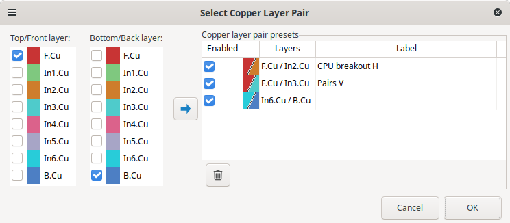
Each can be enabled or disabled, and given an optional user-friendly name.
The enabled presets can be cycled using the Cycle Layer Pair Presets hotkey (Shift+V). If the last-used or current layer pair is not a preset, it is included in the list with the name "Manual".
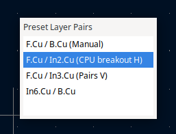
Placing free vias
In addition to placing vias while routing, you can also place standalone vias. These vias connect to items that they touch when they are placed. Free vias may be useful for via stitching, via shielding, thermal design, or other reasons.
To place a free via, click the ![]() button or press Ctrl+Shift+X, then click in the desired location in the editing canvas. If you place a via directly over a track, it will connect to that track as if it was placed while routing: it will take the track’s net, it will create a joint in the track, and dragging the via will also drag the attached tracks.
button or press Ctrl+Shift+X, then click in the desired location in the editing canvas. If you place a via directly over a track, it will connect to that track as if it was placed while routing: it will take the track’s net, it will create a joint in the track, and dragging the via will also drag the attached tracks.
The net assigned to a free via depends on where the via was placed. If the via was placed over a track or pad, it will have the same net as the track, and its Automatically update via nets setting will be enabled so that its net changes with the track’s net. Otherwise, the via will take the net of any zone under the via, if one exists, and its net will not update automatically. If there are multiple zones under the via, you will be prompted to choose which net to use. If there is no zone, the via will not have a net assigned.
修改布线
布线完成后,可以通过移动或拖动来修改它们,或者删除并重新布线。 当选择一个导线时,快捷键 U 可以用来将选择范围扩大到所有连接的导线。 第一次按下 U 将选择与焊盘或过孔最近的连接点之间的导线。 第二次按 U 将再次扩大选择范围,包括所有层上与所选导线相连的所有导线。 用这种技术选择导线可以用来快速删除整个布线网络。
There are two different drag commands that can be used to reposition a track segment. The Drag (45-degree mode) command, hotkey D, is used to drag tracks using the router. If the router mode is set to Shove, dragging with this command will shove nearby tracks. If the router mode is set to Walk Around, dragging with this command will walk around or stop at obstacles. Multiple tracks can be dragged at once using this command. The Drag Free Angle command, hotkey G, is used to split a track segment into two and drag the new corner to any location. Drag Free Angle behaves like the Highlight Collisions router mode: obstacles will not be avoided or shoved, only highlighted.
| 目前还不能拖动包含圆弧的布线。在某些情况下,尝试拖动这些布线会导致圆弧被删除。可以通过选中特定圆弧并使用拖动命令 (D) 来调整其大小。使用此命令调整圆弧大小时,不执行 DRC 检查。 |
移动命令(快捷键 M)也可以在导线上使用。 该命令将拾取选定的导线,而忽略任何未被选中的附加导线或过孔。 使用移动命令移动导线时,不会进行 DRC 检查。
It is also possible to move a footprint while keeping tracks attached to the footprint as it moves. To do so, use the drag command (D) with one or more footprints selected. Any tracks that end at one of the footprint’s pads will be dragged along with the footprints. This feature has some limitations: it only operates in Highlight Collisions mode, so the tracks attached to footprints will not walk around obstacles or shove nearby tracks out of the way. Any DRC violations caused by the drag operation will be highlighted and will be prevent the footprint drag from being committed when you click. To ignore the violations and commit the drag anyway, use Ctrl+click. Additionally, only tracks that end at the origin of the footprint’s pads will be dragged. Tracks that simply pass through the pad or that end on the pad at a location other than the origin will not be dragged.
To delete a track segment, press the Del key. Alternatively, you can use the Backspace key, which deletes a segment and then selects the next segment, allowing you to continue deleting segments one by one; this works in the same way as the Backspace key while routing.
To break a single track segment into two, use the Break tool (right click a track → Break Track). The track will be broken into two connected track segments at the cursor location. Each track segment can then be selected, moved, and edited individually. To recombine the segments into a single segment, drag the drack, or use the merge co-linear tracks option in the Cleanup Tracks and Vias dialog.
Editing track and via properties
You can modify the width of tracks and the size of vias, without re-routing them, in the properties dialog for the track or via. This modifies all selected tracks and vias. The properties dialog shows the relevant properties for the items in the selection: if both tracks and vias are selected, then properties for both types of objects will be displayed, but if only one type of object is selected then properties for the other type of object will not be shown.
| The properties of selected tracks and vias can also be modified using the Properties Manager. |
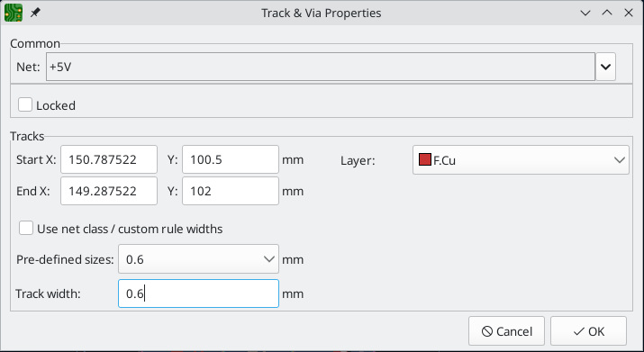
Track and via nets
In the Common section, you can change the assigned net of the selected objects using the Net dropdown. If the Automatically update via nets option is checked, the selected vias cannot have their assigned net manually changed, but instead will be assigned the net of any zone or pad that they touch. You can also lock the selected objects.
Track size, position, and layers
In the Tracks section, you can set the start and end position of the tracks and the layer they are on. You can also change the track width, either from a list of pre-defined sizes or to an arbitrary value.
You can remove the solder mask from on top of tracks on outer layers by enabling the Solder mask checkbox. When enabled, solder mask openings will be drawn for each of the selected tracks with the same shape as the source track. The Expansion textbox controls the size of the mask opening relative to the original track: the expansion value will be added to each side of the original track to form the mask shape. For example, a 1mm wide track with a 1mm expansion would result in a 3mm wide mask cutout, because the 1mm expansion is added to both sides of the track.
Via size, position, and layers
In the Vias section you can change the properties of selected vias. You can change the position of a via, the via’s type (through, micro, blind, or buried), and which layers it spans. Through vias always start and end on the front and back copper layers, but micro vias and blind or buried vias can start and end ony any layers.
You can modify the via annulus and hole diameters, either from a list of pre-defined sizes or to arbitrary values. A via’s diameter and hole size can be defined on a per-layer basis. This is also known as defining the via’s padstack. The Padstack mode controls whether the via shape is the same on all layers or whether individual layers are individually controlled.
-
In the Normal padstack mode, the via’s diameter and hole size are the same on all layers.
-
In the Front/Inner/Back padstack mode, the via’s diameter and hole size can be controlled separately for the front layer, the back layer, and the inner layers (the inner layers will all have the same settings). The Edit layer dropdown controls which layer (or group of layers) is currently being displayed and edited.
-
In the Custom padstack mode, the via’s diameter and hole size can be controlled completely independently on each layer. The Edit layer dropdown controls which layer is currently being displayed and edited.
The Annular rings setting controls which layers will have annular rings for the via.
-
When set to All copper layers, the via will have annular rings on every layer.
-
When set to Start, end, and connected layers, the via will have annular rings on its start and end layers as well as any layer with a track or zone connection to the via. Any layer without track or zone connections, other than the start and end layers, will not have an annular ring.
-
When set to Connected layers only, the via will have annular rings only on layers with a track or zone connection to the via. Any layer without track or zone connections will not have an annular ring.
-
When set to Start and end layers only, the via will have annular rings only on its start and end layers. Zones will not connect to any layers other than the start and end layers. Vias configured in this way are also known as skip vias.
Removing annular rings on unconnected layers reduces the amount of copper in the via barrel. This provides additional routing space on inner layers where the via is not connected, and can also reduce unwanted capacitive coupling between the via and adjacent traces on those layers.
| For dense high-speed designs, using Start, end, and connected layers or Connected layers only can free up routing channels on inner layers. Be aware that some fabricators may require minimum annular ring sizes even on unconnected layers for manufacturing reliability. |
Annular rings can be removed or added in bulk using the Edit Track and Via Properties dialog or by running the Unused Pads tool.
Via protection (IPC-4761)
Vias can receive additional fabrication treatments that affect their physical characteristics. The Protection features dropdown selects a via protection type defined in terms of IPC-4761, which specifies standard combinations of the following treatments:
-
Tenting covers the via with solder mask on one or both sides.
-
Covering adds an additional protective layer (such as epoxy or resin) over the via opening, beyond the standard solder mask.
-
Plugging fills the via hole with non-conductive material (typically epoxy resin) from one or both sides. Plugged vias prevent solder from wicking through the hole during assembly, which is important for via-in-pad designs.
-
Filling completely fills the via hole with conductive material (typically copper or conductive paste), providing maximum thermal and electrical conductivity.
-
Capping places a conductive cap (typically copper plating) over the fill material, creating a flat solderable surface.
The available IPC-4761 protection types in the dropdown are:
| Type | Description |
|---|---|
From rules |
Inherit protection settings from the board-level defaults set in Board Setup. |
None |
No protection applied. |
Type I |
Tented (solder mask only), on one or both sides. |
Type II |
Covered and tented, on one or both sides. |
Type III |
Plugged, on one or both sides. |
Type IV |
Plugged and tented, on one or both sides. |
Type V |
Filled with conductive material. |
Type VI |
Filled and tented, on one or both sides. |
Type VII |
Filled and capped. |
| Via-in-pad designs typically require at least Type IV (plugged and tented) or Type VII (filled and capped). Discuss via treatment requirements with your fabricator early in the design process, as these options significantly affect cost and lead time. |
| The properties of selected tracks and vias can also be modified using the Properties Manager. |
Via backdrilling and post-machining (counterbores and countersinks)
You can configure backdrills and post-machining (counterbores and countersinks) for vias in this dialog. Through-hole pads support the same features in the Pad Properties dialog.
Back-drilling
Back-drilling (also called controlled-depth drilling) is a post-fabrication process that removes the unused portion of a via barrel, known as the via stub. Via stubs can cause signal reflections and resonance at high frequencies, degrading signal integrity. Back-drilling eliminates these stubs by drilling out the plated hole from one or both sides of the board down to a specified layer.
The Back-drill mode setting controls whether and from which side(s) the via will be back-drilled.
| Mode | Description |
|---|---|
No back-drill |
The via is not back-drilled. This is the default. |
Back-drill from bottom |
The unused portion of the via barrel is drilled out from the back (bottom) side of the board. |
Back-drill from top |
The unused portion of the via barrel is drilled out from the front (top) side of the board. |
Back-drill from both |
The via is back-drilled from both the top and bottom sides. This is used when the signal connects on an internal layer and has unused stubs extending in both directions. |
When back-drilling is enabled, you can configure the following parameters for each back-drill side:
-
Back-drill must-cut: The last copper layer through which the back-drill passes. This should be set to the layer just beyond the last connected signal layer to ensure the stub is fully removed while preserving the via connection.
-
Back-drill size: The diameter of the back-drill hole. The back-drill must be larger than the original via hole to fully remove the plating from the barrel walls.
| Back-drilling is most commonly used in high-speed digital designs operating at multi-gigabit data rates, where via stubs longer than a few millimeters can cause measurable signal degradation. Consult your PCB fabricator for their back-drill depth tolerance capabilities. |
Back-drilled vias are shown in the canvas as a ring drawn with the backdrill’s diameter, half in the backdrill’s outer layer color and half in the must-cut layer’s color.
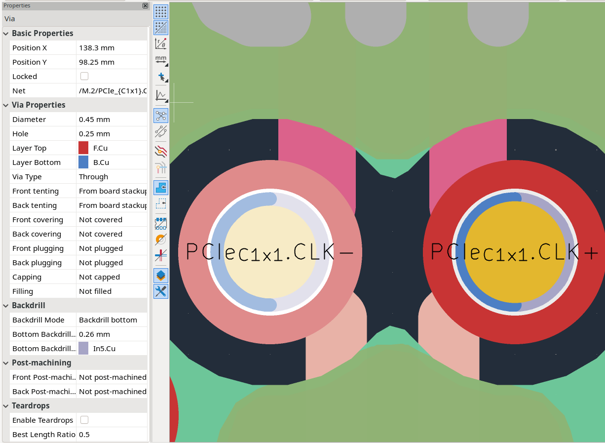
A via with a backdrill shown in the canvas
Post-machining (counterbore and countersink)
Post-machining adds a countersink or counterbore to the front and/or back side of the drill hole. This creates clearance for the head of a fastener installed in the hole. Countersunk holes are conical (angled sides); counterbored holes have straight sides and a flat bottom.
The front and back sides of the via can be configured independently with different post-machining settings.
| Mode | Description |
|---|---|
Not post-machined |
No post-machining is applied. This is the default. |
Counterbore |
A flat-bottomed cylindrical recess is cut into the board surface around the drill hole. This creates a stepped hole profile, typically used to recess a bolt head or provide a flat seating surface. |
Countersink |
A conical recess is cut into the board surface around the drill hole. This creates an angled opening, typically used for flat-head screws that need to sit flush with or below the board surface. |
The following parameters can be configured for each post-machining operation:
-
Size: The diameter of the counterbore or the outer diameter of the countersink at the board surface.
-
Depth: (Counterbore only) The depth of the counterbore recess measured from the board surface.
-
Angle: (Countersink only) The included angle of the countersink cone, in degrees. Common values are 82, 90, and 100 degrees.
| Not all PCB fabricators support post-machining operations; check with your fabricator before specifying these features. |
Post-machined vias are shown in the canvas with additional dashed rings drawn around them. Each dashed ring represents the intersection of the post-machined feature with a copper layer. The color of each dashed circle represents the intersecting layer.
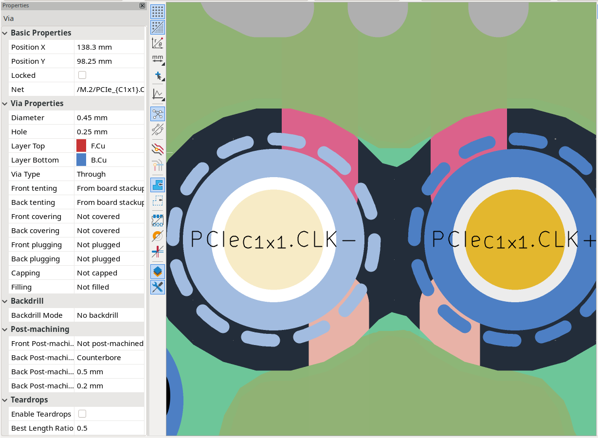
Left: via with countersink. Right: via with counterbore.
Via teardrops
You can configure teardrops for vias in this dialog. Teardrop properties are explained in the Teardrops section.
Bulk editing tracks and vias
To modify tracks and vias in bulk you can use the Edit Track and Via Properties dialog (Edit → Edit Track & Via Properties…)..
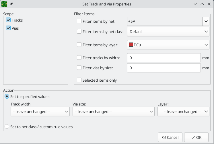
Scope settings restrict the tool to editing only tracks, vias, or both. Vias can be additionally filtered by via type. If no scopes are selected, nothing will be edited.
Filter Items restricts the tool to editing particular objects in the selected scope.
Objects will only be modified if they match all enabled and relevant filters
(some filters do not apply to certain types of objects. For example, via diameter
filters do not apply to tracks). If no filters are enabled, all objects in the
selected scope will be modified. For filters with a text box, wildcards are
supported: * matches any characters, and ? matches any single character.
-
Filter items by net filters to items assigned the specified net.
-
Filter items by net class filters to items assigned to the specified net class.
-
Filter items by layer filters to items on the specified board layer.
-
Filter tracks by width filters to tracks with the specified track width.
-
Filter vias by diameter filters to vias with the specified diameter.
-
Selected items only filters to the current selection.
The Action section determines what editing actions are performed on the filtered objects.
-
When Set to net class / custom rule values is selected, the filtered objects are adjusted to match the values specified by the net class values and custom design rules.
-
When Set to specified values is selected, you can choose which properties to modify and how to set each property. For each property, you can choose
-- leave unchanged --to preserve objects' existing values for that property, or select a new value from the dropdown menu.The editable properties for tracks are:
-
Layer.
-
Track width. The options are defined in Board Setup’s Pre-defined Sizes.
The editable properties for vias are:
-
Via size. The options are defined in Board Setup’s Pre-defined Sizes.
-
Removing unused pads
You can quickly remove unused annular rings from pads and vias using the Unused Pads tool (Tools → Remove Unused Pads…). This will leave annular rings in place on layers where they are used and remove them on layers where they are not used. An annular ring is considered unused if there are no track or zone connections to the pad/via on that layer.
The Remove Unused Layers button removes all unused annular rings from pads and vias that meet the selected filter settings. The Restore All Layers button restores all annular rings to the pads and vias that meet the selected filter settings.
The checkboxes filter which objects will be modified (annular rings removed or restored) and which layers will be removed for those objects.
-
If the Vias checkbox is enabled, annular rings for vias will be modified.
-
If the Pads checkbox is enabled, annular rings for pads will be modified.
-
If the Selected only checkbox is enabled, only selected vias and pads will have their annular rings modified. If it is disabled, annular rings for all vias and pads will be modified. This setting applies in combination with the Vias and Pads checkboxes; for example, a selected via will not be modified if the Via checkbox is disabled.
-
If the Keep outside layers checkbox is enabled, the pad or via’s start and end layers will remain, even if they are unused.
Cleaning up tracks and vias
There is a dedicated tool for performing common cleanup operations on tracks and vias, which is run via Tools → Cleanup Tracks & Vias….
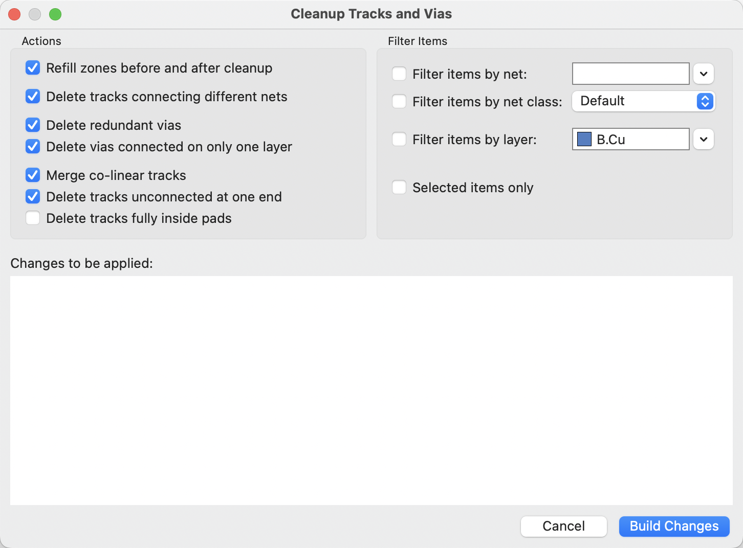
The following cleanup actions are available and will be performed when selected:
-
Refill zones before and after cleanup: refills all zones both before and after the cleanup operation. If unchecked, zone fills will not be changed.
-
Delete tracks connecting different nets: removes any track segments that short multiple nets.
-
Delete redundant vias: remove vias that are redundant because they are located on top of another via or on top of a through hole pad.
-
Delete vias connected on only one layer: removes vias that are only connected to copper on a single layer and are therefore unnecessary.
-
Merge co-linear tracks: merges any track segments that are connected and co-linear into a single equivalent track segment.
-
Delete tracks unconnected at one end: removes track segments that have at least one dangling end.
-
Delete tracks fully inside pads: removes tracks that have both start and end points within a pad and are therefore unnecessary.
You can also filter the objects that will be cleaned up by net, netclass, layer, or selection.
-
Filter items by net: limits the cleanup to tracks and vias assigned to the specified net.
-
Filter items by netclass: limits the cleanup to tracks and vias in the specified netclass.
-
Filter items by layer: limits the cleanup to tracks and vias on the specified layer.
-
Selected items only: limits the cleanup to just the selected tracks and vias.
Any changes that will be applied to the board are displayed at the bottom of the dialog after clicking the Build Changes button. After building the changes, the button changes to say Update PCB. The changes are not applied until you press the Update PCB button.
Routing Convenience Functions
KiCad offers several functions to make certain routing operations more convenient.
If you need to route a number of tracks from a set of pads, you can use the Route Selected tool to quickly route from each pad in sequence. Select the pads you want to use as starting points, then right click and choose Route Selected (Shift+X) to route from each pad in sequence. The router will begin a track from the first selected pad, which you can route as you would any other track. You can also select footprints instead of pads; all unrouted pads in the selected footprints will be used as starting points. When you complete the first track, the router will automatically begin a new track from the next pad in the selection, in the same order that you selected the pads. Pads that already have tracks attached are skipped. You can skip routing the current track and move on to the next pad by right clicking and choosing Cancel Current Item, Pressing Esc (or right clicking and pressing Cancel) skips the rest of the operation, leaving any already-completed tracks as they are.
If you want to route a number of tracks to a set of pads, instead of from the pads, you can use the Route Selected From Other End tool. Select the pads you want to use as ending points, then right click and choose Route Selected From Other End (Shift+E). This tool works the same way as the Route Selected tool, except it uses each selected pad as an end point rather than a starting point. The starting point for each track is the other end of the ratsnest line for each selected pad.
Routing from the other end is also possible while routing individual tracks: press Ctrl+E while routing a track to commit the current segment and begin routing from the other end of the in-progress track’s ratsnest line.
Finally, you can quickly unroute tracks connected to an object (footprint, pad, or track) by selecting the object, right-clicking, and choosing Unroute Selected. Any tracks connected to the selected object will be removed, starting at the selected object and continuing until another pad is encountered.
Automatically completing tracks
KiCad’s router can automatically route individual tracks, based on the connections defined in the schematic. This can be thought of as a limited form of auto-routing that considers a single track at a time. The router will only use the current layer; it will not use vias or change layers.
While routing, press the F key to have the router attempt to automatically finish the current track. The track will be automatically routed from the end of the last fixed track segment to the closest ratsnest anchor. If the router can’t automatically finish the track, it will allow you to complete the track manually. This action can also be performed by clicking Attempt Finish in the context menu while routing.
When the router is not the active tool, you can automatically route multiple tracks by selecting footprints, pads, and tracks to route from, right clicking, and choosing Attempt Finish Selected (Autoroute) (Shift+F). You do not need to select both ends of a desired connection; the router will route from the selected item to its nearest ratsnest anchor. If multiple items were selected, each item will be routed in sequence, in the order that they were selected. If a connection cannot be automatically completed, the tool will pause with the router active so that you can complete the track manually. With the automatic completion paused for a manual connection, you can skip the current track and move on to routing the next track by right clicking and choosing Cancel Current Item. After manually completing the track or skipping the connection, the tool will continue attempting to route the remaining connections. Pressing Esc (or right clicking and pressing Cancel) skips the rest of the operation, leaving any already-completed tracks as they are.
差分对布线
Differential pairs in KiCad are defined as nets with a common base name and a positive and negative suffix. KiCad supports using + and -, or P and N as the suffix. For example, the nets USB+ and USB- form a differential pair, as do the nets USB_P and USB_N. In the first example, the base name is USB, and USB_ in the second. The suffix styles cannot be mixed: the nets USB+ and USB_N do not form a differential pair. Make sure you name your differential pair nets accordingly in the schematic in order to allow use of the differential pair router in the PCB editor.
要对差分对进行布线,请点击差分对布线 ![]() 图标(从绘图工具栏或从顶部工具栏 布线 下)或使用快捷键 6。 点击一个焊盘、过孔或现有差分对线段的末端,开始布线。 你可以从差分对的正网络或负网络开始布线。
图标(从绘图工具栏或从顶部工具栏 布线 下)或使用快捷键 6。 点击一个焊盘、过孔或现有差分对线段的末端,开始布线。 你可以从差分对的正网络或负网络开始布线。
差分对布线器将尝试用设计规则中的间隙规则进行布线(差分对间隙可以在电路板设置对话框的 “网络类” 部分中配置,也可以通过使用自定义设计规则来配置)。如果布线的起始或结束位置与配置的间隙不同,布线器将创建一个较短的 "扇出" 部分,以最大限度地缩短差分对未耦合的布线长度。
当切换层或使用 放置过孔 (V) 操作时,差分对布线器将创建两个相邻的过孔。这些过孔将被放置在尽可能靠近彼此的位置,同时遵守铜的间隙规则以及孔到孔的间隙规则。
长度调整
The length tuning tools can be used to add serpentine tuning shapes to tracks after routing. Length tuning shapes are persistent objects that can be modified after they are created. Both length tuning and time-domain (delay) tuning are supported; both forms of tuning use the same tools. To tune the length of a track, first pick the appropriate tool.
-
The single-track length tuning tool (icon
 or hotkey 7) will add serpentine shapes to bring the length (or time delay) of a single track up to the target value.
 -
The differential pair length tuning tool (icon
 or hotkey 8) will do the same for a differential pair.
 -
The differential pair skew tuning tool (icon
 or hotkey 9) will add length to the shorter member of a differential pair in order to eliminate skew (phase difference) between the positive and negative sides of the pair.
As with the Routing icons, the Tuning icons are found in both the Route menu dropdown from the top toolbar and the drawing toolbar on the right.
The process for tuning a track is as follows:
-
If desired, configure the target length and skew using custom DRC rules. If you do not set up the target length or skew using DRC rules, you will need to manually add a target length after creating the tuning pattern.
-
Activate one of the tuning tools as described above. The appropriate tool depends on the type of tuning you need to achieve (single-track length, differential pair length, or differential pair skew).
-
Hover over tracks in the board to show a status window that displays the current length or skew, together with the target values.
-
Click on the desired track to start tuning it.
-
Move the mouse cursor along the track to interactively add meander shapes. The popup window next to the cursor shows a live measure of the length or skew compared to the design targets.
-
While you tune, you can adjust the tuning pattern’s spacing and amplitude to fine-tune the length and change how the pattern fits on the board. Press 1 and 2 to increase/decrease the spacing, and 3 and 4 to increase/decreaase the amplitude.
-
If you have set a target length, the tool will stop adding meanders when the target length is reached. You can set a target length with custom DRC rules or in the tuning shape properties; both methods are explained below.
-
Click in the canvas to commit the tuned shape. The tuned track doesn’t need to be perfect because you can adjust the shape after committing it. You can also place multiple tuning shapes on the same track.
| The length tuning tools only support tuning the length of point-to-point nets between two pads. Tuning the length of nets with different topologies is not supported. |
| Differential pair length tuning can only be applied to the coupled portions of differential pairs. To apply length tuning to the uncoupled portions of differential pairs, you must use single-track length tuner. |
Editing tuning patterns
After a tuning pattern has been added, it can be selected, modified, and moved. While it is selected, the target length and routed length are shown in the message panel at the bottom left of the window.
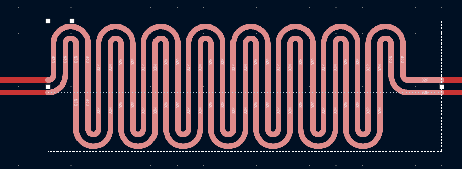
When a pattern is selected, editing handles appear, which let you adjust the pattern geometry.
-
Dragging the handles at the ends of the pattern will expand or contract the pattern along the track.
-
Dragging the corner handle towards or away from the track will respectively decrease or increase the maximum meander amplitude.
-
The final handle controls the meander spacing; dragging it towards the corner handle will increase the spacing, while dragging it away from the corner handle will increase the spacing.
The selection box and editing handles represent the maximum allowable extents of the tuning pattern. Making the box smaller will reduce the size of the tuning pattern, even if this results in the tuned track being shorter than the target length. When the box is enlarged, the tuning pattern will expand to fill the box until the target length is reached.
You can move a tuning pattern along its track by selecting it and dragging with the mouse, or using the Move tool (M). Deleting a tuning pattern (Del) removes the tuning pattern and restores the original untuned tracks. You can also ungroup the tuning pattern, which will decompose it into its component tracks. The basic tracks have the same shape as the tuning pattern but can be edited individually. Once ungrouped into tracks, a tuning pattern cannot be regrouped.
Another way to edit a tuning pattern is through its properties dialog. The properties dialog exposes several additional parameters that can’t be modified using the on-canvas interactive editor. These properties can also be edited in the Properties Manager.
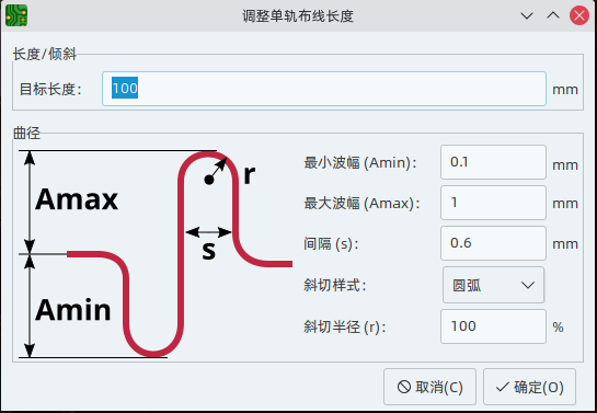
As with the interactive editor, you can set a maximum amplitude for the tuning pattern and a spacing between meanders, but here you can set a minimum amplitude and configure the corner style. Corners can be filleted (rounded) or chamfered. In each case you can set the radius as a percentage of the maximum possible radius for the spacing and amplitude. You can also configure the tuning pattern to be single-sided, which restricts it to one side of the baseline, as opposed to the default style which positions meanders on both sides of the baseline.
You can set default values for these properties in the Design Rules → Length-tuning Patterns page of the Board Setup dialog. Each type of tuning pattern (single track length, differential pair length, and differential pair skew) can have its own defaults.
Finally, the tuning pattern properties dialog is one of two ways to set the target length or skew for a tuning pattern. Setting length targets is explained below.
Setting target length and skew
There are two ways to set a target length or skew for a net:
-
In the properties dialog for a tuning pattern that has already been added to a track.
-
Using a custom DRC rule with the
lengthand/orskewconstraints.
The first method is to specify a target in the tuning pattern’s properties dialog. For length tuning, this is the Target Length or Target Delay field, depending on whether you are tuning the physical length or tuning in the time domain. For skew tuning, this is the Target Skew or Target Delay Skew field. This target will only apply to the selected tuning pattern. Therefore, length targets set in this way must be set separately for each tuning pattern in the design. The properties dialog for a tuning pattern is only accessible after the pattern is initially created, so changing a target length or skew in this way may require the pattern to be adjusted to meet the new target value, if the pattern’s geometric constraints do not allow sufficient space to meet the new target.
You can also set a target length and/or skew using custom design rules. If custom rules are used, they will override any targets set in tuning pattern properties, unless the override custom rules checkbox is enabled in the tuning pattern properties.
Using a custom rule allows you to set a net’s target length and/or skew up front, before a pattern is created. With custom rules you can set different length and skew targets based on specific criteria, such as netclass or net name. You will also result in a DRC violation if the net’s length or skew is out of bounds.
When target length or skew is adjusted in a custom DRC rule after a pattern is created, the pattern geometry will not be automatically updated to achieve the new target. You can use Edit → Update All Tuning Patterns to recalculate all tuning patterns to meet the new targets.
The following example custom rule sets a target length and skew for nets in the high_speed netclass. The target length is 100mm, and a DRC error will be raised if it is below 95mm or above 105mm. The target skew is at most 0.1mm.
(rule "target length and skew"
      (condition "A.hasNetclass('high_speed')")
      (constraint length (min 95mm) (opt 100mm) (max 105mm))
      (constraint skew (max 0.1mm)))
See the custom rule documentation for more details of how to create rules that only apply to certain nets.
Length tuning pitfalls and tips
The length tuner only tunes nets with a point-to-point topology; branching nets are not supported. When the length tuner encounters a branch, it stops at the branch and only considers the length of the net up to that branch.
Sometimes you may end up with leftover stub tracks somewhere in your design. These can turn what appears to be a point-to-point net into a branched topology, which will prevent length tuning from working as expected. It may be easier to find such stub tracks when you switch footprints, vias, and tracks to outline mode (![]() ,
, ![]() , and
, and ![]() buttons, respectively). You can also use the track cleanup tool (Tools → Cleanup Tracks and Vias…) to remove many of these stubs automatically.
buttons, respectively). You can also use the track cleanup tool (Tools → Cleanup Tracks and Vias…) to remove many of these stubs automatically.
By default, the length tuner includes vias in its length calculations. Only the layer-to-layer length of the via is used, which may be shorter than the full top-to-bottom via height if the tuned path is not exclusively on the board top and bottom. The accuracy of this calculation depends on the board stackup being accurately configured. Via length can be ignored in length tuner calculations by deselecting include stackup height in track length calculations in the Constraints page of the Board Setup dialog.
The length tuner is optimized for adjusting the effective electrical distance between two points, and therefore it calculates net length in a slightly different way than other tools, such as the Net Inspector. In addition to discounting net branches and unused portions of vias, the length tuner also optimizes paths through pads to use the shortest possible path in its calculations. In comparison, the Net Inspector reports a simple summation of copper segment lengths. Both calculations are accurate, but they are optimized for different purposes. These differences are discussed in more detail in the Net Inspector documentation.
Time-domain tuning (propagation delay)
Traditional length tuning matches the physical trace length of nets so that all routed paths are the same distance. This works well when all traces in a group are routed on the same layer with the same geometry, because every trace has the same propagation velocity and equal lengths produce equal delays.
In many real-world designs, however, signals travel through multiple board layers with different stackup geometries. A trace on an outer layer (microstrip) has a different propagation velocity from a trace on an inner layer (stripline), because the effective dielectric constant surrounding the conductor differs between the two geometries. When a net group contains traces routed on a mix of layers, matching physical length alone does not guarantee that all signals arrive at the same time.
Time-domain tuning solves this problem by matching propagation delay instead of physical length. The length tuner calculates the signal delay through every segment of the path — tracks, vias, and pad-to-die connections — using per-layer propagation parameters that you define in a tuning profile. Meander shapes are then added or adjusted until the total propagation delay meets the target, rather than matching a target length.
When to use each mode
Length-domain tuning is appropriate when:
-
All traces in the matched group are on the same layer.
-
The board stackup is simple (e.g., two-layer board) and propagation velocity differences between layers are negligible.
-
The design requirements specify matched lengths rather than matched delays.
Time-domain tuning is appropriate when:
-
Matched nets are routed across multiple layers (e.g., signals that transition between outer and inner layers with vias).
-
The board stackup causes meaningful differences in propagation velocity between layers (e.g., a high-layer-count design with both microstrip and stripline routing).
-
The design requirements specify matched delays or flight times (common in DDR memory, PCIe, USB, and other high-speed interfaces).
| Even if your design appears to have all traces on one layer, enabling time-domain tuning accounts for via transitions and pad-to-die delays that pure length matching ignores. For the most accurate timing analysis on high-speed buses, prefer time-domain tuning. |
How time-domain tuning works
When time-domain tuning is active for a net, the length tuner replaces its length-based calculations with delay-based calculations. The overall propagation delay for a routed path is the sum of three components:
- Track delay
-
For each trace segment, the delay is calculated by multiplying the segment’s physical length by the per-layer unit delay (propagation delay per unit distance) defined in the tuning profile. Because each layer can have a different unit delay, traces on different layers contribute different amounts of delay per unit of physical length.
- Via delay
-
Each via contributes a propagation delay based on the distance the signal travels through the via (determined from the board stackup) and the via’s unit delay. The tuning profile defines a global via unit delay and allows per-layer-pair overrides for situations where different via transitions have different electrical characteristics.
- Pad-to-die delay
-
If a pad has a pad-to-die length or pad-to-die delay configured in its padstack properties, this value is included in the total delay calculation.
The length tuner displays the total propagation delay in the status window when you hover over a net with a time-domain tuning profile active. The target is shown in time units (picoseconds) instead of length units.
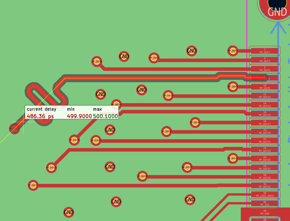
Board stackup and delay calculations
Accurate time-domain tuning depends on a correctly configured board stackup. The stackup defines the physical distances between copper layers, which determines via heights, and the dielectric properties of each layer, which affect propagation velocity calculations.
Configure your stackup in Board Setup → Physical Stackup. Ensure that:
-
The number of copper layers is correct.
-
Dielectric materials and thicknesses are set to match your fabrication stackup.
-
Prepreg and core thicknesses are accurate, as they directly affect the calculated impedance and propagation delay for each signal layer.
The tuning profile’s built-in calculator uses the stackup to automatically determine unit delay values for each signal layer. If you recalculate delay values after changing the stackup, the new dielectric properties will be taken into account.
| The stackup must be configured before creating tuning profiles. If you change the stackup after setting up tuning profiles, you should recalculate the delay values in your tuning profiles to reflect the updated geometry. |
Propagation delay calculation details
KiCad’s propagation delay calculation engine processes the routed path of a net and applies several optimizations to determine the true electrical path:
-
The path through a via is optimized so that only the portion between the layers actually used by the routed signal is counted. If a through via connects traces on
F.CuandIn1.Cu, only the stackup distance between those two layers contributes to the via delay, not the full via height fromF.CutoB.Cu. -
Contiguous track segments on the same layer are merged into single line chains before delay calculation, ensuring that segment boundaries do not introduce calculation artifacts.
-
Where a track enters a pad, the electrical path is clipped to the shortest distance through the pad shape rather than using the full track length to the pad center. This gives a more accurate representation of the actual signal path.
These optimizations ensure that the delay calculation closely matches the true electrical path of the signal.
Per-layer delay tracking
When time-domain tuning is active, the delay engine tracks delay contributions on a per-layer basis. This means that for a net routed on multiple layers, you can see how much delay is contributed by each layer individually. This per-layer detail is available in the View → Panels → Net Inspector panel; enable Show Time Domain Details from the Net Inspector’s settings menu to switch the per-layer columns from length to delay values. This can help identify which layer transitions are contributing the most to timing skew in a group of matched nets.
Setting target delay
There are two ways to set a target propagation delay for a net:
-
In the properties dialog for a tuning pattern, select the Delay radio button and enter a value in the Target Delay field. The delay is specified in picoseconds.
-
Using a custom DRC rule with the
lengthorskewconstraint and time-based units (e.g.,psfor picoseconds).
When using custom DRC rules, specifying the constraint value in time units automatically switches the length tuner to time-domain mode for matching nets. For example:
(rule "DDR data delay matching"
      (condition "A.hasNetclass('DDR_DATA')")
      (constraint length (min 450ps) (opt 500ps) (max 550ps)))
This rule sets a target propagation delay of 500 ps for all nets in the DDR_DATA netclass, with an allowable range of 450 ps to 550 ps. A DRC violation will be raised for any net outside this range.
You can also set delay-based skew constraints for differential pairs:
(rule "DDR differential skew"
      (condition "A.hasNetclass('DDR_CLK')")
      (constraint skew (max 5ps)))
When a custom DRC rule uses time units, the constraint operates in the time
domain. When it uses length units, it operates in the length (space) domain.
You cannot mix time and length units within the min, opt, and max fields
of a single constraint.
|
Practical example: DDR4 memory bus
A DDR4 data bus typically requires tight delay matching between all data signals in a byte lane. Consider a design with the following characteristics:
-
Data signals routed on
F.Cu(microstrip) andIn1.Cu(stripline) -
Layer change via from
F.CutoIn1.Cu -
Target delay matching of 500 ps +/- 50 ps
To set up time-domain tuning for this scenario:
-
Configure the board stackup in Board Setup → Physical Stackup with accurate dielectric thicknesses and materials. Use 6 layers for this example with GND on In1.Cu and In4.Cu.
-
Create a tuning profile in Board Setup → Design Rules → Tuning Profiles. Name it
DDR4_Data, select Single, and check Enable time domain tuning. -
In the Track Propagation table, add rows for
F.CuandIn2.Cu. Select appropriate reference layers and press the button to auto-calculate the unit delay for each layer.
 -
In the Via Propagation section, set the global via unit delay or add a specific override for the
F.CutoIn2.Cutransition. -
Assign the
DDR4_Datatuning profile to your DDR data net class in the Net Classes page. -
Add a custom DRC rule to set the target delay:
(rule "DDR4 data delay" (condition "A.hasNetclass('DDR4_Data')") (constraint length (min 450ps) (opt 500ps) (max 550ps))) -
Use the length tuning tools to tune the data nets. The tuner will display delay in picoseconds and add meanders until the target delay is met.
DRC integration
DRC validates both length-domain and time-domain tuning constraints. When a custom DRC rule specifies a length or skew constraint in time units, DRC checks the calculated propagation delay of each matching net against the specified bounds.
In addition, tuning profiles generate implicit DRC rules that enforce track geometry. When a tuning profile is assigned to a net class, DRC can verify that tracks on each layer match the width (and differential pair gap) defined in the tuning profile. The severity of these geometry checks is controlled by the Tuning profile track geometries violation type in the Violation Severity page of Board Setup. By default this check is disabled (set to Ignore); set it to Warning or Error to enable it.
If a net class references a tuning profile that does not exist (for example, if a profile was deleted), DRC raises a Missing tuning profile violation.
Teardrops
Teardrops are areas of extra copper that smooth the transition between tracks and pads, vias, or other tracks with different width. Teardrops are added to increase the mechanical robustness of a track connection. They also reduce the risk of a misaligned drill hole disconnecting a track from a drilled pad or via.
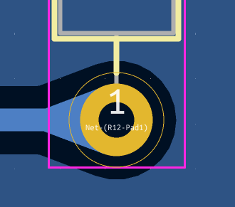
There are two ways to add teardrops to your design. You can add them in bulk using the Edit Teardrops dialog, or you can add them to individual pads and vias in the respective properties of the pad or via.
Adding teardrops in bulk
The Edit Teardrops dialog (Edit → Edit Teardrops…) lets you add teardrops to many board objects at once. The dialog has controls for filtering which objects are affected and settings for configuring the shape of the new teardrops. It also lets you edit or remove existing teardrops.
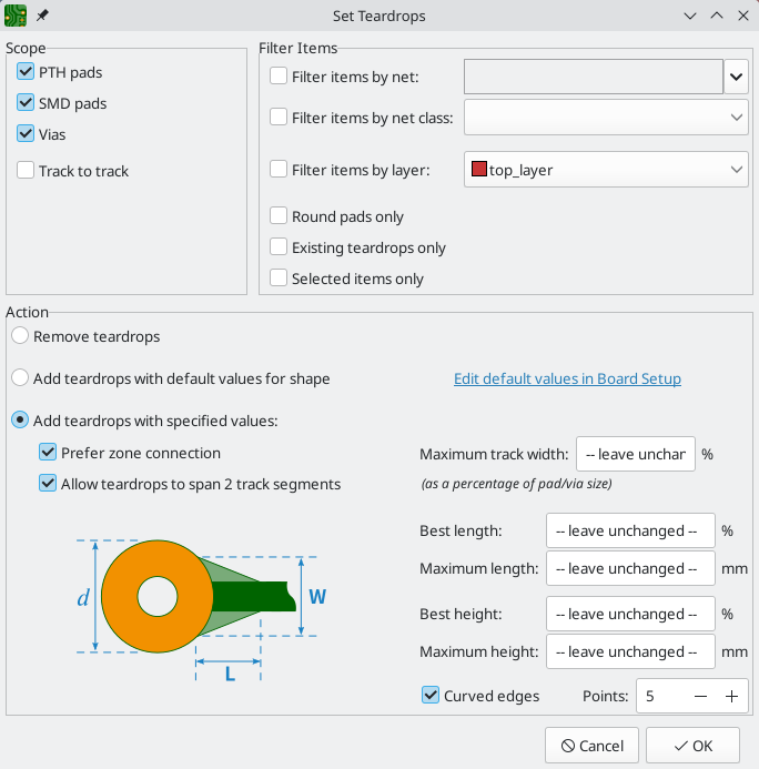
The Scope section controls which types of objects will be affected: PTH pads, SMD pads, vias, and/or track-to-track connections. The Filter Items section lets you filter objects by other criteria; you can filter items by net, net class, and layer, or choose to act only on round pads, pre-existing teardrops, or the objects in your selection.
The Action section controls whether to add or remove teardrops, as well as the size and shape of the new teardrops.
Remove Teardrops will remove teardrops that match the scope and filtering options at the top of the dialog. Remove All Teardrops will remove all teardrops on the board, even if they do not match the scope and filters.
Add teardrops with default values for shape will add teardrops with the configured default teardrop settings to every board object that matches the scope and filters. To configure the default teardrop settings, click the Edit default values in Board Setup link or manually open the Teardrops panel in Board Setup. The defaults are configured separately for teardrops connecting to round shapes, rectangular shapes, or between tracks.
Instead of using the default values, you can provide custom teardrop settings by selecting Add teardrops with specified values. The available teardrop settings are:
-
Prefer zone connection: if selected, a teardrop will not be created if the object is also connected to a zone.
-
Allow teardrops to span 2 track segments: if selected, the teardrop will be able to spread over a second track segment if the first segment is too short to support a full teardrop.
-
Maximum track width: a teardrop will not be created for a track connection that is wider than this percentage of the pad width (minimum pad dimension).
-
Best length: the ideal length of the teardrop, as a percentage of the width (smallest dimension) of the attached object.
-
Maximum length: the maximum length of the teardrop, as an absolute length.
-
Best width: the ideal width of the teardrop, as a percentage of the width (smallest dimension) of the attached object.
-
Maximum width: the maximum width of the teardrop, as an absolute width.
-
Curved edges: if selected, the teardrop edges will be curved instead of a straight line.
Adding a teardrop to an object that already has a teardrop will update the existing teardrop with the new settings. However, you can leave any existing teardrop setting in an object unchanged by setting the value to -- leave unchanged -- in a textbox, or by selecting the third, indeterminate state for a checkbox. Any value set this way will not be updated in the targeted objects' teardrop settings.
Adding teardrops to individual objects
Rather than in bulk, you can add or edit teardrops for individual vias in the properties dialog for that via, or for individual pads in the Connections tab of the pad’s properties dialog. The settings in the properties dialogs are the same as in the Edit Teardrops dialog. You can also edit teardrops for individual pads and vias with the Properties Manager.
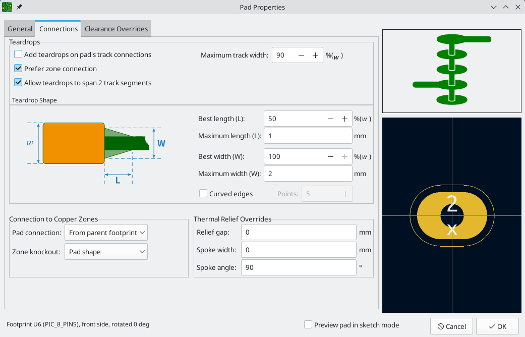
Other details about teardrops
Teardrops in KiCad are small zones, meaning that when they refill they avoid shorting to copper objects on other nets. They are initially filled when they are added, but they are unfilled and refilled with other zones on the board: when using the Unfill All Zones and Refill All Zones commands, running DRC, generating fabrication outputs, etc. Teardrops can be shown in filled or outline mode using the zone display controls in the left toolbar.
Teardrops can be added to any type of pad, including custom pads. Some custom pad shapes may produce undesirable teardrop shapes. In those cases, it may be preferable to disable teardrop generation for those specific pads.
Backdrills and hole post-machining (counterbores/countersinks)
Backdrilling and post-machining are post-fabrication steps that can be applied to vias and through-hole pads.
Backdrilling (also called controlled-depth drilling) removes the unused portion of a plated hole barrel, known as the stub. Stubs can cause signal reflections and resonance at high frequencies, degrading signal integrity. Backdrilling eliminates stubs by re-drilling the plated hole from one or both sides of the board down to a specified layer. The enlarged diameter must be large enough to completely remove the plating on the hole wall.
Post-machining adds a countersink or counterbore to the front and/or back side of an existing pad or via hole. This creates clearance for the head of a fastener installed in the hole. Countersunk holes are conical, meaning the sides of the cutout are angled. Counterbored holes have straight sides and a flat bottom.
Backdrills
You can add backdrills to vias using the Via Properties dialog (see Back-drilling for detailed settings) and to pads using the Backdrill tab of the Pad Properties dialog.
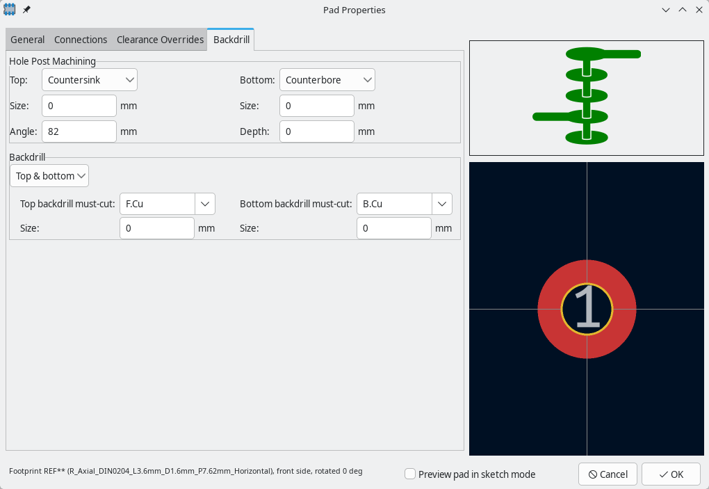
The Back-drill mode setting controls whether and from which side(s) the pad or via will be back-drilled.
| Mode | Description |
|---|---|
No back-drill |
The hole is not back-drilled. This is the default. |
Back-drill from bottom |
The unused portion of the barrel is drilled out from the back (bottom) side of the board. |
Back-drill from top |
The unused portion of the barrel is drilled out from the front (top) side of the board. |
Back-drill from both |
The hole is back-drilled from both the top and bottom sides. This is used when the signal connects on an internal layer and has unused stubs extending in both directions. |
When back-drilling is enabled, you can configure the following parameters for each back-drill side:
-
Back-drill must-cut: The last copper layer through which the back-drill passes. This should be set to the layer just beyond the last connected signal layer to ensure the stub is fully removed while preserving the connection.
-
Back-drill size: The diameter of the back-drill hole. The back-drill must be larger than the original hole to fully remove the plating from the barrel walls.
Backdrills are shown in the canvas as a ring drawn with the backdrill’s diameter, half in the backdrill’s outer layer color and half in the must-cut layer’s color. For pads, the pad layer after the must-cut layer is drawn below the backdrill ring.

A pad with a backdrill from F.Cu (red) to In3.Cu (cyan). In4.Cu (magenta) is shown as the primary pad color.
Post-machining holes (counterbores and countersinks)
You can add counterbores or countersinks to vias using the Via Properties dialog (see Post-machining for detailed settings) and to pads using the Backdrill tab of the Pad Properties dialog.
The front and back sides of the hole can be configured independently with different post-machining settings.
| Mode | Description |
|---|---|
Not post-machined |
No post-machining is applied. This is the default. |
Counterbore |
A flat-bottomed cylindrical recess is cut into the board surface around the drill hole. This creates a stepped hole profile, typically used to recess a bolt head or provide a flat seating surface. |
Countersink |
A conical recess is cut into the board surface around the drill hole. This creates an angled opening, typically used for flat-head screws that need to sit flush with or below the board surface. |
The following parameters can be configured for each post-machining operation:
-
Size: The diameter of the counterbore or the outer diameter of the countersink at the board surface.
-
Depth: (Counterbore only) The depth of the counterbore recess measured from the board surface.
-
Angle: (Countersink only) The included angle of the countersink cone, in degrees. Common values are 82, 90, and 100 degrees.
Post-machined pads are shown in the canvas with additional dashed rings drawn around them. Each dashed ring represents the intersection of the post-machined feature with a copper layer. The color of each dashed circle represents the intersecting layer.
Left: via with countersink. Right: via with counterbore.
Graphics and text
Graphical objects (lines, arcs, rectangles, circles, polygons, text, tables, dimensions, barcodes, and points) can exist on any layer. They exist primarily for aesthetics and documentation, although shapes on copper layers can make electrical connections and have nets assigned.
Graphical shapes
Graphical shapes are geometric objects that can be drawn on any board layer.
When they are drawn on copper layers, graphical objects can be assigned nets and make connections to other copper objects, much like tracks and zones. There are differences between copper shapes and tracks or zones, however:
-
The shape of a graphical object is exactly defined by its own properties (size, position, line width, fill, etc.) and is not affected by other nearby objects. In contrast, a zone fills the area within a specified outline, but avoids different-net copper items to automatically maintain a specified clearance.
-
Graphic lines and arcs are edited as simple shapes; the interactive router is not used for drawing or modifying them. Therefore collisions with other items are not detected interactively as they would be when routing tracks (although they will be detected by DRC).
The buttons on the right toolbar can be used to create:
-
Lines (
 , default hotkey Ctrl+Shift+L)
 -
Arcs (
 , default hotkey Ctrl+Shift+A)
 -
Bezier curves (
 , default hotkey Ctrl+Shift+B)
 -
Rectangles and rounded rectangles (
 )
) -
Circles (
 , default hotkey Ctrl+Shift+C)
 -
Polygons (
 , default hotkey Ctrl+Shift+P)
To place a shape, select the tool, then click in the canvas to place the shape’s first point. Click again to place the shape’s second point. For rectangles and circles, placing the second point will fully define the shape and finish drawing it. Some shapes require three or more points to be placed, however. Arcs require three points, while lines, polygons and bezier curves can accept an arbitrary number of points, and require a double click to complete.
To modify an existing graphical object, select it, then drag its editing handles to change the shape. Moving a handle at the corner of a shape will move that corner. Moving a handle on the edge of a shape will move that edge in a direction perpendicular to the edge. Normally, dragging an edge maintains the angles of the corners adjacent to the edge while allowing the edge’s length to vary. Holding Ctrl instead holds the edge’s length constant and allows the adjacent corner angles to vary.
| Dragging the corner of a polygon displays the angle of that corner and the two adjacent corners. |
To precisely position a corner, right click the corner’s handle and choose Shape Modification → Move Corner To…, then enter new X and Y coordinates for the corner. For polygons, there is an additional tool that lets you edit the coordinates of each outline point as a table, which you can open by right clicking the polygon and choosing Shape Modification → Edit Corners…. This opens a floating dialog with a table containing the coordinates of every corner. Editing the coordinates of a corner immediately updates the polygon.
Just like with tracks, you can expand a selection from one graphic line to include all other contiguous graphic lines by pressing U.
Arc editing modes
Arcs have three vertex editing modes, which are selectable in Preferences → PCB Editor → Editing Options or by right clicking the ![]() button on the right toolbar. You can also cycle between the modes with the Ctrl+Space hotkey.
button on the right toolbar. You can also cycle between the modes with the Ctrl+Space hotkey.
-
Keep arc center, adjust radius maintains the position of the arc center as as the arc endpoints or midpoint are dragged, changing the radius as necessary.
-
Keep arc endpoints or direction of starting point maintains the position of the arc endpoints and the arc’s direction of curvature as the midpoint or center are dragged.
-
Keep arc radius and center, adjust angle maintains the radius and the position of the center of the arc as the arc’s endpoints are dragged, changing the arc’s angle.
Editing shape properties
The properties of a graphic shape can be adjusted in the shape’s properties dialog or with the Properties Manager.
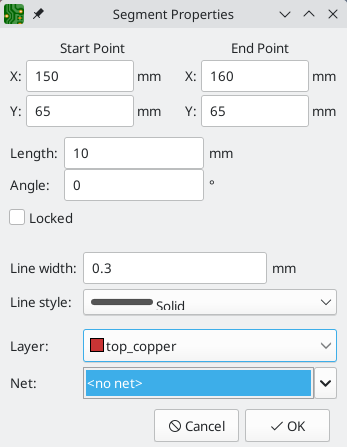
-
The top section contains controls for editing the object’s location and shape. Some types of objects can be edited in multiple ways, with each method in its own tab. For example, a line segment can be edited by its start and end points, by its start point, length, and angle, or by its start and mid points.
-
Locked controls whether or not the text object is locked. Locked objects may not be manipulated or moved, and cannot be selected unless the Locked Items option is enabled in the Selection Filter panel.
-
Rectangles can have their corners rounded by checking the Rounded rectangle checkbox. The corner radius can be adjusted with the Corner radius parameter or by dragging the radius handle in the editing canvas. Rounding the corners of a rectangle is a non-destructive action: the corner radius can be adjusted or removed at any time.
-
The Line width option controls the width of the outline, even for filled objects. The outline width extends on both sides of the "ideal" shape of the graphic object. For example, a graphic circle that is defined to have 2mm radius and 0.2mm line width will consist of a torus with an outer radius of 2.1mm and inner radius of 1.9mm. If the shape is filled and the line width is set to 0, the shape will be a filled circle with 2mm radius. Several line styles are available in the Line style dropdown: solid, dashed, dotted, dash-dot, and dash-dot-dot.
| You can customize the default style of newly-created graphical shapes in the Text & Graphics Defaults section of the Board Setup dialog. |
-
Closed shapes (rectangles, circles, and polygons) can be outlines or filled shapes, which is controlled by the Filled shape checkbox.
-
The Layer dropdown controls which layer the shape is placed on. Graphical shapes on copper layers can have a net assigned in their properties dialog. Copper shapes with a net make connections like tracks or zones. Unlike zones, copper graphical objects always maintain their shape and do not keep clearance to other copper objects.
-
When shapes are placed on outer copper layers, they can be configured to affect the corresponding solder mask layer in addition to their primary copper layer by enabling the Solder mask checkbox. When enabled, a shape on the front copper layer will also be drawn on the front solder mask layer, while a back copper shape will also be drawn on the back solder mask layer. Because solder mask layers are negative, this will result in a solder mask opening with the same shape as the copper shape. The Expansion textbox controls the size of the mask opening relative to the original copper shape: the expansion value will be added to each side of the original shape to form the mask shape. For example, a 1mm wide copper segment with a 1mm expansion would result in a 3mm wide mask cutout, because the 1mm expansion is added to both sides of the segment.
Shape modification tools
KiCad has several tools for modifying combinations of graphic shapes in useful ways, such as chamfering two lines or combining two polygons. These tools are used by selecting the shapes or corners you want to modify, right clicking, and then choosing the relevant tool in the Shape Modification submenu. Different tools are available for different combinations of selected shapes or corners.
-
Heal Shapes fixes a discontinuity between two lines or arcs. A new line segment is added to connect the ends of each shape together, up to a specified tolerance.
-
Simplify Polygons removes superfluous corners from the selected shape with a configurable tolerance. Corners are removed if they are more than the specified distance from the line between their two neighboring corners.
-
Fillet Lines adds an arc to round the corner between two connected lines with a specified radius. The two original lines are shortened to meet the endpoints of the arc. Note that for rectangles, you can instead round the corners by turning the rectangle into a rounded rectangle.
-
Chamfer Lines adds a line segment to create a new edge between two connected lines with a specified setback. The two original lines are shortened to meet the endpoints of the new segment.
-
Dogbone Corners adds circular reliefs to the corners of the selected shapes. This is similar to filleting, but the modified shape is larger than the original, with the added arcs intersecting the vertices of the original corners. In other words, the added reliefs exactly enclose the original corners. This can be useful for relieving the corners of interior cutouts so that they can be manufactured using a round cutting tool. Because dogbones are intended to allow interior corners to be manufactured, a dogbone is only added to a corner if the corner points into the body of the board as defined by the board outline. There is an option to Add slots to acute corners, which adds extended slots in corners that are too narrow to reach with a cutting tool of the selected radius.
-
Extend Lines to Meet lengthens two selected lines until they intersect each other. The two lines will share a coincident endpoint.
-
Move Corner To moves the selected corner to a specific X and Y coordinate.
-
Move Midpoint To moves the selected midpoint to a specific X and Y coordinate, maintaining the line’s slope and moving the adjacent corners as necessary.
-
Create Corner adds a new corner to the outline while maintaining the original outline shape.
-
Remove Corner deletes the selected corner from the outline.
-
Chamfer Corner deletes the selected corner and adds new corners next to the original corner so that the original corner shape becomes chamfered.
-
Edit Corners opens a dialog to edit the coordinates of the selected shape’s corners.
-
Merge Polygons combines two or more selected polygons into one new polygon that is the union of the original shapes.
-
Subtract Polygons subtracts one or more polygons from another polygon, resulting in a new polygon that is the difference of the original shapes. The first-selected polygon(s) are subtracted from the last-selected polygon.
-
Intersect Polygons results in a new polygon that is the shape of the overlapping area between two or more selected polygons.
Converting objects to and from graphic shapes
KiCad provides tools to convert graphic objects to other types of objects, other types of objects to graphic objects, and graphic objects to other kinds of graphic objects. These tools are used by selecting the shapes you want to convert, right clicking, and then choosing the desired result object from the Create From Selection submenu. Most types of object conversions have several conversion options that are presented in a settings dialog. The exact options differ based on the target object type.
When converting to a graphic polygon, rule area, or zone, there are several options for how to convert the source objects into a polygonal outline.
-
If copy line width of first object is selected, an unfilled polygon will be created that has its line width taken from the line width of the first selected source object. This option is only available when converting to a graphic polygon, and the source object must be a closed shape.
-
If use centerlines is selected, an object with zero line width will be created, with its outline placed at the centerlines of the source objects. The source object must be a closed shape. If the target object is a graphic polygon, it will be filled.
-
If create bounding hull is selected, an object will be created with the specified line width. The object’s outline will be offset from the outermost extents of the source object by the specified gap. The source object does not need to be a closed shape when a bounding hull is created.
Most conversions provide a delete source objects after conversion option, which will result in the original object being deleted during the conversion, only leaving the new object in place. If this option is not selected, the conversion will leave the original object in place in addition to the new object. The original object will be selected following the conversion so that it can be manually deleted by pressing Delete.
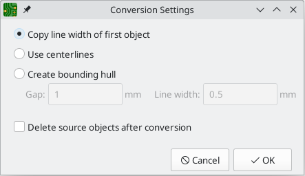
The following conversion types are available:
-
Create Polygon From Selection converts a graphic shape, text, zone, rule area, or track into a polygon. This can be used to convert separate graphic shapes, such as lines and arcs, into a unified shape. It can also be used to convert a text object into a shape that can have its outline manipulated graphically.
-
Create Zone From Selection converts a graphic shape, text, zone, rule area, or track into a zone. In addition to the conversion settings, the conversion dialog also shows options for configuring the resulting zone. This can be used to create zone outlines with complex shapes, such as curves, that would otherwise be difficult to create using the zone tool.
-
Create Rule Area From Selection converts a graphic shape, text, zone, rule area, or track into a rule area. In addition to the conversion settings, the conversion dialog also shows options for configuring the resulting rule area. This can be used to create rule area outlines with complex shapes, such as curves, that would otherwise be difficult to create using the rule area tool.
-
Create Lines From Selection converts a graphic polygon or rectangle into graphic lines that follow the source shape’s outline. This can be used to convert a unified shape into its constituent outline segments.
-
Create Outsets From Selection converts the selected object (graphic shapes, pads, etc.) into a rectangle that surrounds the original shape with some spacing.
The outset tool can be used to quickly create outlines, courtyards, etc., especially in combination with other shape modification tools. -
The Outset distance specifies the minimum distance between the outset and the original shape. There will always be at least this much space between the two shapes. If the distance is positive, the outset will be larger than the original shape. If the distance is negative, the outset will be smaller than the original shape.
-
If Round corners (when possible) is enabled, the outset will have rounded corners rather than being a simple rectangle.
-
If Round outwards to grid multiples (when possible) is enabled, the outset will be placed on the specified grid, rounding outwards when necessary so that the specified outset distance is maintained.
-
If Copy item layers is enabled, the outset will be drawn on the same layer as the original shape. If disabled, the outset will be drawn on the layer selected in the dropdown menu.
-
If Copy item thickness (when possible) is enabled, the outset will be drawn with the original item’s thickness if that item has a thickness, or the specified thickness otherwise. Some source items, like pads, do not have a thickness property. The specified thickness will always be used when this option is disabled.
-
-
Create Tracks From Selection converts a graphic shape, zone, or rule area into tracks that follow the source shape’s outline. If the source object is not on a copper layer, a dialog will be presented to specify the target copper layer. The source object is not removed following conversion, but remains selected so that it can be easily deleted if desired.
-
Create Arc From Selection converts a graphic line segment or track segment into a graphic arc. The arc’s endpoints are placed at the endpoints of the source segment and its thickness is taken from the source object’s line thickness. The source segment is not removed following conversion, but remains selected so that it can be easily deleted if desired.
Importing vector graphics
You can add graphic shapes from an external vector graphics file by importing the file into KiCad. DXF and SVG files are supported. To import the file, use File → Import → Graphics… (Ctrl+Shift+F).
| You can also import a vector graphics file by dragging and dropping it onto the editing canvas. |
Imported vector graphics are part of the design like any other graphic shape. In other words, they have an assigned board layer, they are included in fabrication outputs, and shapes on copper layers can make electrical connections.
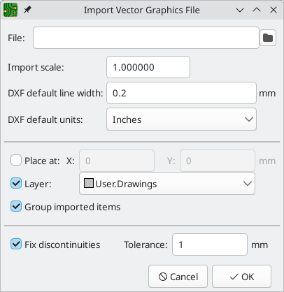
The Import Vector Graphics File dialog has several options:
-
File specifies the vector graphics file to import.
-
Import Scale sets the scale factor for the import.
-
DXF default line width sets the line width for any items in a DXF file that do not specify a line width. It has no effect when not importing DXF files.
-
DXF default units sets the default unit for DXF files with unspecified units. It has no effect when not importing DXF files.
-
If Place At is enabled, the imported shapes are placed at the specified location, relative to the PCB Editor’s page origin. If it is disabled, the imported shapes are placed interactively.
-
If Layer is enabled, the imported shapes are placed onto the selected layer. If it is disabled, the shapes are placed onto the active layer.
-
If Group imported items is enabled, all shapes imported from the vector graphics file are added to a group.
-
If Fix discontinuities is enabled, any shape discontinuities smaller than the specified tolerance are filled by extending each segment until they intersect or adding an additional segment.
Text objects
Graphical text may be placed by using the ![]() button in the right toolbar or by keyboard shortcut Ctrl+Shift+T. Activating the tool brings up a text properties dialog. After configuring the text and its properties and accepting the dialog, you can click in the canvas to place the text.
button in the right toolbar or by keyboard shortcut Ctrl+Shift+T. Activating the tool brings up a text properties dialog. After configuring the text and its properties and accepting the dialog, you can click in the canvas to place the text.
You can also add text boxes, which are similar to regular text except that they have an optional border and they automatically reflow text within that border. Text boxes are placed with the ![]() button, and require clicking twice to specify the top left and bottom right corners of the box.
button, and require clicking twice to specify the top left and bottom right corners of the box.
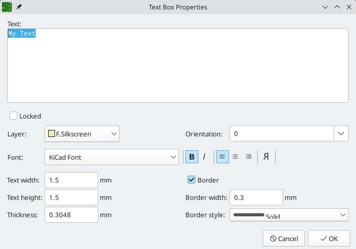
-
Locked controls whether or not the text object is locked. Locked objects may not be manipulated or moved, and cannot be selected unless the Locked Items option is enabled in the Selection Filter panel.
-
Layer controls the text’s layer. Text may be placed on any layer, but note that text on copper layers cannot be associated with a net and cannot form connections to tracks or pads. Copper zones will fill around the rectangular bounding box of text objects.
-
There are several formatting options: text can be bolded, italicized, left/right/center aligned, top/bottom/center aligned, and reversed.
-
The knockout option adds a solid rectangle surrounding the text and makes the text itself a negative cutout. This feature is only available for regular text objects, not text boxes.
-
The Font dropdown lets you select a font for the text. You can use any TTF font available on your system, or the built-in KiCad stroke font.
| User fonts are not embedded by default in the project. If the project is opened on another computer that does not have the selected font installed, a different font will be substituted. You can optionally embed into the board file any fonts used by the design in the Embedded Files section of Board Setup. For maximum compatibility without embedding, use the KiCad font. Also consider converting text objects to polygons before sharing a project (right click a text object → Create from Selection → Create Polygon from Selection…). Text converted to polygons is not editable as text, but will render identically on any computer. |
-
You can adjust the text size with the Text width and Text height controls. When you are using the KiCad font, you can also adjust the stroke width with the Thickness control. When the
 button is pressed the text thickness is automatically adjusted according to the text size: the thickness for normal text is set to the size divided by 8, and the thickness for bold text is set to the size divided by 5.
 -
Position X and position Y control the text object’s location. These properties are not available for text boxes.
-
Orientation is the rotation angle of the text object. You can select an angle in 90 degree increments from the dropdown, or type in an arbitrary angle.
Text boxes additionally have options controlling their border.
-
The border checkbox makes the border visible or invisible. For visible borders, you can adjust the border’s thickness with the border width control and the line style with the border style control (solid, dashed, dotted, dash-dot, or dash-dot-dot).
-
The margins between the border and the text on each side of a text box can be set using the Properties Manager. Margins cannot be set in the Text Box Properties dialog.
| You can customize the default style of newly-created text objects in the Text & Graphics Defaults section of the Board Setup dialog. |
Finally, text supports markup for superscripts, subscripts, overbars, evaluating project variables, and accessing symbol field values.
| Feature | Markup Syntax | Result |
|---|---|---|
Superscript |
|
textsuperscript |
Subscript |
|
textsubscript |
Overbar |
|
text |
|
variable_value |
|
|
field_value of symbol refdes |
| Project text variables must be defined in Board Setup before they can be used. There are also a number of built-in text variables. |
Tables
You can use a table to organize text in a tabular format. Tables have customizable borders, cell sizes, and headers, and can be placed on any layer.
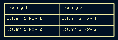
To place a table, use the ![]() button in the right toolbar. Click in the canvas to place the top left corner of the table, then click again to place the bottom right corner of the table and finish drawing the table. The bigger you draw the table, the more rows and columns will be added by default, but rows and columns can be added or deleted after the table is created.
button in the right toolbar. Click in the canvas to place the top left corner of the table, then click again to place the bottom right corner of the table and finish drawing the table. The bigger you draw the table, the more rows and columns will be added by default, but rows and columns can be added or deleted after the table is created.
Once you have created a table, you can edit the table as a whole or edit cells individually. Creating a new table automatically opens the Table Properties dialog to edit the entire table.
You can export a table from KiCad into a CSV file by right clicking a table or table cell and clicking Export Table to CSV….
Editing a whole table
You can edit an entire table with the Table Properties dialog. There are several ways to open the Table Properties dialog:
-
Create a new table. The Table Properties dialog opens automatically when the table is created.
-
Select any cell in the table, right click, and select Edit Table (Ctrl + E).
-
Select the entire table, right click, and select Properties… (E). You can select the entire table with a drag selection or by selecting a single cell, then right clicking and selecting Select Table.
-
Click the Edit Table… button in the Table Cell Properties dialog.
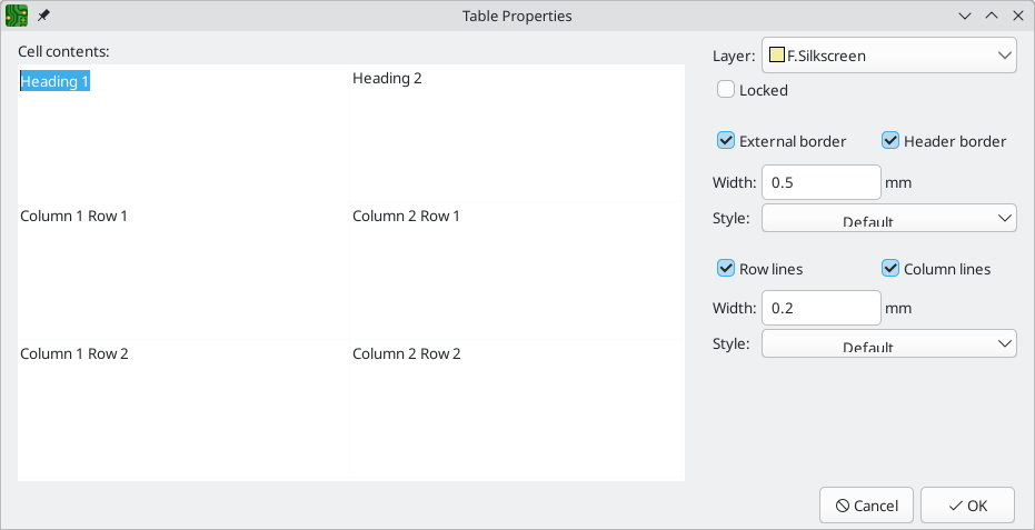
This dialog lets you edit the properties of the entire table, including the text in each cell and the separators between cells. To change the formatting of text in a cell, edit the properties of individual cells, instead of the properties for the entire table.
| The properties for a table can also be edited in the Properties Manager when the entire table is selected. |
The left side of the dialog displays an editable grid of the entire table. You can edit the contents of any cell by clicking on the cell in the grid. You can also edit the text in a cell by selecting the cell and using the Properties Manager. If you have tabular content in a spreadsheet or other table, you can copy and paste that content into the grid here.
| Text in table cells supports the markup described in the text objects section (superscripts, subscripts, strikethroughs, etc.). |
The right side of the dialog contains formatting options for the table.
-
The Layer dropdown controls which board layer the table is on.
-
The Locked checkbox controls whether or not the table is locked. Locked objects may not be manipulated or moved, and cannot be selected unless the Locked Items option is enabled in the Selection Filter panel.
-
The External border and Header border checkboxes control whether there is a border drawn around the entire table and the cells in the top row, respectively. When Header border is enabled, the border below the cells in the top row is styled using these external border settings rather than the row/column line settings. The line width of the header borders is controlled by the Width field. The line style can be set to solid, dashed, dotted, dash-dot, or dash-dot-dot using the Style dropdown menu.
-
The Row Lines and Column lines checkboxes enable horizontal lines between rows and vertical lines between columns, respectively. These have the same formatting options as the external and header borders.
Editing individual table cells
Instead of editing the properties of an entire table, you can also edit the properties of individual cells. This modifies selected cells, but does not affect other cells. To open the Table Cell Properties dialog, double click on a cell, or select a cell, right click, and choose Properties… (E). If you select multiple cells, the properties dialog will act on all of them at once.
| You can select multiple cells by clicking and dragging. |
| To select all cells in a row or column, select a cell in that row or column, right click, and choose Select Row(s) or Select Column(s). You can select multiple rows or columns in this way by starting with multiple cells selected. |
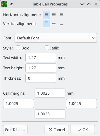
The left side of the dialog lets you edit the contents of the selected cell. The right side of the dialog contains formatting options for the selected cell.
-
The Font dropdown lets you select a font for the text. You can use any TTF font available on your system, or the built-in KiCad stroke font.
-
There are several formatting options: text can be bolded, italicized, left/right/center aligned, and top/bottom/center aligned.
-
You can adjust the text size with the Text width and Text height controls. When you are using the KiCad font, you can also adjust the stroke width with the Thickness control. When the
button is pressed the text thickness is automatically adjusted according to the text size: the thickness for normal text is set to the size divided by 8, and the thickness for bold text is set to the size divided by 5. -
The Cell margins textboxes control the amount of spacing around the top, bottom, left, and right of the text in the cell.
You can click the Edit Table… button to open the properties dialog for the entire table.
| The properties for a table cell can also be edited in the Properties Manager when one or more table cells is selected. |
Editing table layout
The layout of a table (size and number of columns and rows) is initially set when you create a table, but you can also edit the layout after creation.
To resize a row or column, select a cell in that row or column, then drag the handle on the right (to change the column width) or the bottom (to change the row height) to the desired size.
To add rows or columns, select a cell next to where the new row or column should go, right click, then choose Add Row Above, Add Row Below, Add Column Before, or Add Column After, as desired.
To delete rows or columns, select a cell in the row or column you want to delete, then right click and choose Delete Row(s) or Delete Column(s). To delete multiple rows or columns, start with a selection that spans all the rows or columns you want to delete.
You can merge multiple cells into a single cell by selecting all the cells you want to merge, right clicking, and choosing Merge Cells. To unmerge them, select the merged cell, right click, and choose Unmerge Cells.
尺寸标注
尺寸标注是用于显示测量值或电路板设计上的其他标记的图形对象。 它们可以被添加到任何绘图层中,但通常被添加到某个用户层。 KiCad 目前支持五种不同类型的标注:对齐、正交、中心、径向和引线。
-
Aligned dimensions (
 ) show a measurement of
distance between two points. The measurement axis is the line that connects those two points, and
the dimension graphics are kept parallel to that axis.
) show a measurement of
distance between two points. The measurement axis is the line that connects those two points, and
the dimension graphics are kept parallel to that axis. -
Orthogonal dimensions (
 ) also measure the
distance between two points, but the measurement axis is either the X or Y axis. In other words,
these dimensions show the horizontal or vertical component of the distance between two points.
When creating orthogonal dimensions, you can select which axis to use as the measurement axis based
on where you place the dimension after selecting the two points to measure.
) also measure the
distance between two points, but the measurement axis is either the X or Y axis. In other words,
these dimensions show the horizontal or vertical component of the distance between two points.
When creating orthogonal dimensions, you can select which axis to use as the measurement axis based
on where you place the dimension after selecting the two points to measure. -
Center dimensions (
 ) create a cross mark to
indicate a point or the center of a circle or arc.
) create a cross mark to
indicate a point or the center of a circle or arc. -
Radial dimensions (
 ) show a measurement between
a center point and the outside of a circle or arc. The center point is indicated by a cross.
) show a measurement between
a center point and the outside of a circle or arc. The center point is indicated by a cross. -
Leader dimensions (
 ) create an arrow with a leader line
connected to a text field. This text field can contain any text, and an optional circular or
rectangular frame around the text. This type of dimension is often used to call attention to parts
of the design for reference in fabrication notes.
) create an arrow with a leader line
connected to a text field. This text field can contain any text, and an optional circular or
rectangular frame around the text. This type of dimension is often used to call attention to parts
of the design for reference in fabrication notes.
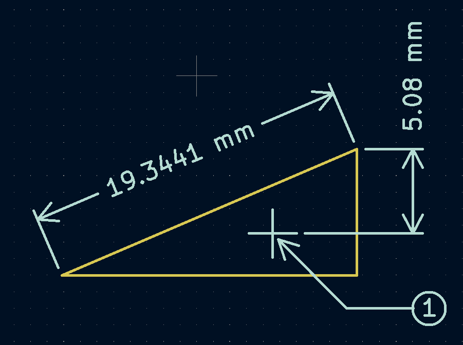
创建一个尺寸标注后,可以编辑其属性(快捷键 E)以改变显示数字的格式以及文本和图形线的风格。
| You can customize the default style of newly-created dimension objects in the Text & Graphics Defaults section of the Board Setup dialog. |
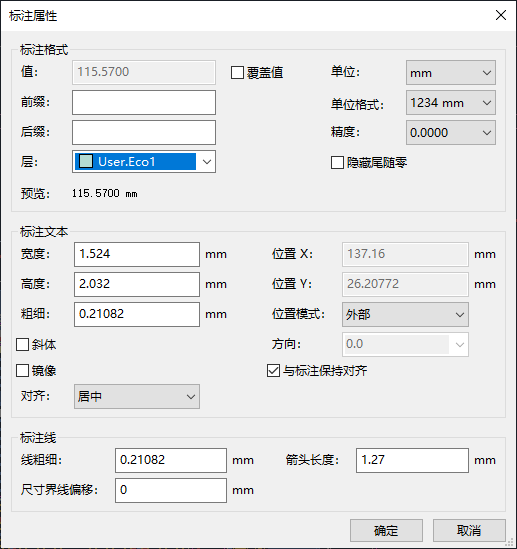
尺寸标注格式选项
-
Override value: When enabled, you may enter a measurement value directly into the Value field that will be used instead of the actual measured value.
-
Prefix: Any text entered here will be shown before the measurement value.
-
Suffix: Any text entered here will be shown after the measurement value.
-
Layer: Selects which layer the dimension object exists on.
-
Units: Selects which units to display the measured value in. Automatic units will result in the dimension units changing when the display units of the board editor are changed.
-
Units format: Select from several built-in styles of unit display.
-
Precision: Select how many digits of precision to display.
-
Suppress trailing zeroes: Select whether to hide trailing zeroes in the value text.
尺寸标注文本选项
大多数尺寸标注文本选项与其他图形文本对象的选项相同(见上面的图形对象部分)。 也有一些特殊的选项适用于尺寸标注文本:
-
Position mode: Choose whether to position the dimension text manually, or to automatically keep it aligned with the dimension measurement lines.
-
Keep aligned with dimension: When enabled, the orientation of the dimension text will be adjusted automatically to keep the text parallel with the measurement axis.
尺寸标注线选项
-
Line thickness: Sets the thickness of the graphical lines that make up a dimension’s shape.
-
Arrow length: Sets the length of the arrow segments of the dimension’s shape. A negative arrow length reverses the arrow direction.
-
Arrow direction: Select whether the dimension object’s arrow(s) point inwards towards the value text or outwards away from the text. The arrow direction can also be set while drawing a dimension by right clicking and selecting Switch Dimension Arrows.
-
Extension line offset: Sets the distance from the measurement point to the start of the extension lines.
-
Extension line overshoot: Sets the distance from the dimension’s line to the end of the extension lines.
引线选项
Leader dimensions have unique options:
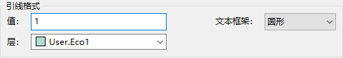
-
Value: Enter the text to show at the end of the leader line.
-
Text frame: Select the desired border around the text (circle, rectangle, or none).
Barcodes
KiCad has a tool for generating barcodes and adding them to the board. Barcodes can be placed on any layer. Five types of barcodes are supported, including QR codes.
To add a barcode, click the ![]() button on the right toolbar, then click in the canvas in the desired location. The Barcode Properties dialog appears, where you can enter the details for the barcode. The right side of the dialog displays a preview of the barcode based on the selected options.
button on the right toolbar, then click in the canvas in the desired location. The Barcode Properties dialog appears, where you can enter the details for the barcode. The right side of the dialog displays a preview of the barcode based on the selected options.
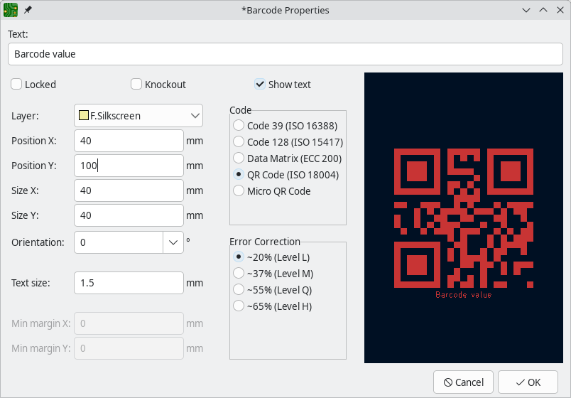
-
Text is the data to be encoded in the barcode. If the Show text checkbox is checked, the text will also be printed verbatim below the barcode.
-
If Locked is checked, the barcode is created as a locked object.
-
If Knockout is checked, a solid margin is added around the barcode, and the barcode is created as a negative cutout from the solid background. Min margin X and Min margin Y control the horizontal and vertical margin around the barcode when knockout mode is selected.
-
Layer selects the board layer on which to place the barcode.
-
Position X and Position Y determine the location of the barcode.
-
Size X and Size Y determine the width and height of the barcode.
-
Orientation sets the rotation angle of the barcode in degrees.
-
Text size controls the size of the text printed below the barcode.
-
The Code options control the type of barcode that is generated. The following barcode types are available:
-
Code 39 (ISO 16388)
-
Code 128 (ISO 15417)
-
Data Matrix (ECC 200)
-
QR Code (ISO 18004)
-
Micro QR Code
-
-
The Error Correction options control the error correction included in the generated barcodes. The error correction options only apply to QR codes and Micro QR codes.
Points
Points are nonphysical, zero-dimensional objects that can be added to a board for reference, documentation, or snapping purposes. Points are not included in exports or fabrication outputs, but are used to mark specific locations in boards and footprints while editing. In addition to visually marking a location, points are snap targets, so you can use them for moving and locating footprints and other objects. For example, a point could be added at a key location in a footprint to help align the footprint to a board feature or to another footprint.

Points are considered to be on a specific board layer. This means you can use the layer display controls to control when they are displayed, when they are selectable, and when they are snappable. The circle surrounding a point in the editing canvas is drawn in the color of the point’s layer. Points also have a size property, which controls their display size in the editing canvas.
To add a point to a PCB, click the ![]() button in the right toolbar, then click in the canvas. The point is added on the current layer. To change the point’s layer or size, use the Properties panel.
button in the right toolbar, then click in the canvas. The point is added on the current layer. To change the point’s layer or size, use the Properties panel.
批量编辑文本和图形
Properties of text and graphics, including footprint fields and dimensions, can be edited in bulk using the Edit Text and Graphics Properties dialog (Edit → Edit Text & Graphic Properties…).
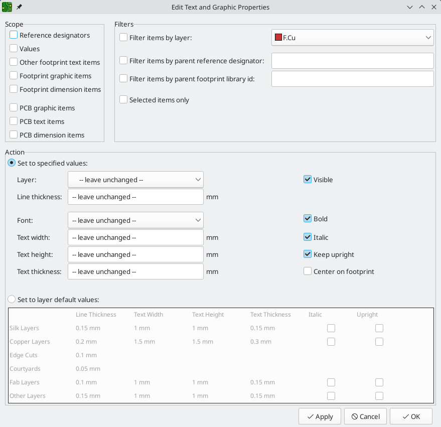
范围和筛选器
Scope settings restrict the tool to editing only certain types of objects. If no scopes are selected, nothing will be edited.
Filters restrict the tool to editing particular objects in the selected scope.
Objects will only be modified if they match all enabled and relevant filters
(some filters do not apply to certain types of objects. For example, parent
footprint filters do not apply to graphic items and are ignored for the purpose
of changing graphic properties). If no filters are enabled, all objects in the
selected scope will be modified. For filters with a text box, wildcards are
supported: * matches any characters, and ? matches any single character.
-
By layer filters to items on the specified board layer.
-
By parent reference designator filters to fields in the footprint with the specified reference designator.
-
By parent footprint library link filters to fields in footprint with the specified library link (library and footprint name).
-
Selected items only filters to the current selection.
操作
被筛选对象的属性可以在对话框的底部设置为新的值。通过选择 设置为指定值,可以将属性设置为任意值,或者通过选择 设置为图层默认值,将属性重置为其图层的默认值。
下拉列表和文本框可以被设置为 --保持不变-- 以保留现有值。复选框可以被选中或不被选中,以启用或禁用某个变化,但也可以切换到第三种 "保持不变" 状态。
-
所有项目都可以设置其 层。
-
图形对象可以修改其 线的粗细。
-
Text properties that can be modified are font, text width, text height, text thickness (KiCad font only), emphasis (bold and italic), orientation (keep upright), and alignment (center on footprint). Footprint fields can also have their visibility set.
Cleaning up graphics
There is a dedicated tool for performing common cleanup operations on graphics, which is run via Tools → Cleanup Graphics….
The following cleanup actions are available and will be performed when selected:
-
Merge lines into rectangles: combines individual graphic lines that together form a rectangle into a single rectangle shape object.
-
Delete redundant graphics: deletes graphics objects that are duplicated or degenerate.
-
Fix discontinuities in board outlines: modifies the existing board outline to fix any discontinuities that are within the specified tolerance.
Any changes that will be applied to the board are displayed at the bottom of the dialog. They are not applied until you press the Update PCB button.
Sheet title block
The drawing sheet’s title block is edited with the Page Settings tool (![]() ). You can also open this tool by double clicking on any part of the drawing sheet.
). You can also open this tool by double clicking on any part of the drawing sheet.
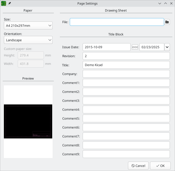
Each field in the title block can be edited, as well as the paper size and orientation.
You can set the date to today’s or any other date by pressing the left arrow button next to Issue Date. Note that the date listed in the board title block is not automatically updated. It is only updated when changed in this dialog.
A drawing sheet file can also be selected to replace the default drawing sheet. When choosing a drawing sheet, you can enable the Embed File checkbox in the file browser to embed the drawing sheet in the board instead of referencing an external file. This means the board will appear the same when it is opened on another computer that does not have the drawing sheet file available at the same external file path. For more information, see the embedded files documentation.
Rule areas (keepouts)
Rule areas, also known as keepouts, are board regions that can have specific DRC rules defined for them. Some basic rules are available that will raise DRC errors if certain types of objects are within the bounds of the rule area, but rule areas can also be used together with custom DRC rules to define complex DRC behavior that only applies within the rule area. Rule areas are also used to define channels for multichannel layout.
You can add a rule area by clicking the ![]() button on the right toolbar (Ctrl+Shift+K). Click on the canvas to place the first corner, which will show the Rule Area Properties dialog. After configuring the rule area appropriately, press OK to continue placing corners of the rule area. The rule area shape can be an arbitrary polygon; click on the starting corner or double click to finish placing the rule area.
button on the right toolbar (Ctrl+Shift+K). Click on the canvas to place the first corner, which will show the Rule Area Properties dialog. After configuring the rule area appropriately, press OK to continue placing corners of the rule area. The rule area shape can be an arbitrary polygon; click on the starting corner or double click to finish placing the rule area.
To modify an existing rule area outline, select it, then drag its editing handles to change the shape. Moving a handle at the corner of a rule area will move that corner. Moving a handle on the edge of a rule area will move that edge in a direction perpendicular to the edge. Normally, dragging an edge maintains the angles of the corners adjacent to the edge while allowing the edge’s length to vary. Holding Ctrl instead holds the edge’s length constant and allows the adjacent corner angles to vary.
To precisely position a corner, right click the corner’s handle and choose Shape Modification → Move Corner To…, then enter new X and Y coordinates for the corner. You can also edit the coordinates of every outline corner by right clicking the rule area and choosing Shape Modification → Edit Corners…. This opens a floating dialog with a table containing the coordinates of every corner. Editing the coordinates of a corner immediately updates the rule area.
| You can also create rule areas by converting an existing graphic shape to a rule area. This can be useful, for example, for creating a rule area with a shape that would otherwise be difficult to draw with the rule area tool, such as a circle. To convert a shape to a rule area, right click the shape, then select Create from Selection → Create Rule Area from Selection…. |
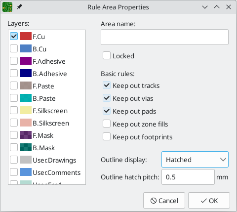
The Rule Area Properties dialog has the following options:
-
The layers list determines which layers the rule area applies to. The area only appears on these layers and the selected keepout rules only apply on these layers. At least one layer must be selected. By default, the active layer in the editing canvas is preselected in the rule area layer list.
-
The area name field is optional and provides an identifier for the rule area. If it is provided, it is included in DRC violation messages to make them clearer. It can also be used in custom DRC rules to identify a particular rule area.
-
The locked checkbox determines if the rule area should be locked. As with other objects, rule areas can also be locked or unlocked after they are created.
-
The Keepouts tab contains several basic rules to prevent various types of objects from being placed within the rule area. The basic rules can be configured to keep out tracks, vias, pads, zone fills, and/or footprints. If an object of one of the selected types is within the rule area, a DRC error will be raised. Additionally, zone fills will automatically avoid a rule area if the rule area is configured to keep out zones.
| Even with no basic rules selected, rule areas can still be used to define specific areas in which to apply custom DRC rules. |
-
The Placement tab contains settings for multichannel layout, which are explained in that section.
-
There are a few options for the outline display of the rule area. The area can be shown with a hatched outline, fully hatched throughout the area, or with just the outline with no hatching. The outline hatch pitch is also adjustable.
锁定
Locking an item makes it more difficult to select, move, or modify the object, which can prevent unintended modifications. Most objects can be locked through their properties dialogs, by using the right-click context menu, or by using the Toggle Lock hotkey (L).
Some actions are restricted for locked objects:
-
Locked objects cannot be selected unless the Locked items checkbox is enabled in the selection filter.
-
Even when selected, locked objects cannot be moved unless the Override locks checkbox is enabled in the top toolbar. When it is enabled, locked items can be moved in the same way as unlocked items. When it is disabled, locked items cannot be moved. If you attempt to move a selection that includes locked items, the locked items will be deselected and not moved. Any remaining unlocked items are moved as normal.
Locked items are displayed with a colored shadow around them. The color can be customized in your color scheme, and the shadow can be hidden in the Objects tab of the Appearance panel.
| Locked objects can’t be selected unless the Locked items checkbox is enabled in the selection filter, or moved unless the Override locks checkbox is enabled. By default, these checkboxes are disabled. |
Groups
Groups let you treat multiple objects as a single object for the purposes of moving or rotating them. Each object in the group will maintain its position relative to the other objects in the group. When objects are grouped, it is difficult to accidentally edit them or move them relative to the other members of the group. Groups can have a name, which is displayed in the editing canvas when the group is selected.
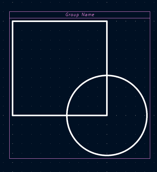
Most types of objects in the Board Editor can be grouped: footprints, tracks, zones, graphic items, and even other groups. Groups can contain multiple different types of objects at once.
To add objects to a group, select them, then right click and choose Grouping → Group Items, or click the ![]() button in the top toolbar. To remove all items from a group, select the group, right click, and choose Grouping → Ungroup Items, or click the
button in the top toolbar. To remove all items from a group, select the group, right click, and choose Grouping → Ungroup Items, or click the ![]() button in the top toolbar.
button in the top toolbar.
Once objects have been added to a group, selecting any of the objects will select the group as a whole instead of the constituent objects. To edit a specific object within a group, first select the group, the right click and choose Enter Group. Double clicking on a group also enters the group. When a group has been entered, objects within the group can be selected and edited individually without affecting the other objects in the group. To leave the group and stop editing its members individually, right click and select Leave Group, select an object outside the group, or use Esc.
There are several ways to modify which objects belong to a group. To remove objects from an existing group, enter the group, then select the objects you want to remove, right click, and choose Grouping → Remove Items. To add items to a group, first ungroup all the items from the group. This will leave the group’s former members selected. Then add the new item to the selection and group the selection. Note that without first ungrouping, this process would create a nested group: a new group containing the new item and the entire original group, not just the items in the original group.
You can also add or remove objects from a group in the group’s properties dialog. To open a group’s properties dialog, press E or right click and click Properties…. The properties dialog lists the objects contained in the group. To add an additional object to the group, click the ![]() button, then click on the desired object in the editing canvas. The object you click on will be added to the group. To remove an object, select it in the list, then click the
button, then click on the desired object in the editing canvas. The object you click on will be added to the group. To remove an object, select it in the list, then click the ![]() button.
button.
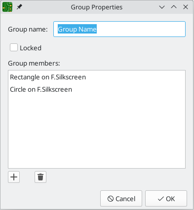
The group properties dialog also lets you specify a name for the group or lock the group. Groups can also be named or locked using the Properties Manager.
The Library link field is used for design blocks. It specifies the group’s linked design block name and library in the format <library>:<block>. This field must be filled out correctly to link design block layout groups to the corresponding block in the schematic and in the design block library.
Aligning objects
The align tool moves a selection of objects so that they are all aligned with a reference object. There are six different alignments to choose from, depending on which part of the objects you wish to align. Objects can be horizontally aligned by their left, center, or right edges, or they can be vertically aligned by their top, center, or bottom edges. Objects are only moved in one dimension, so objects stay in the same horizontal position when aligned vertically, and vice versa. To align objects by a given edge, select the objects, then right click and choose Align/Distribute → Align to Left (or another alignment as desired).
If the cursor is over an object in the selection, that object is used as the reference object. Otherwise, the reference object is the object in the selection which is located furthest in the alignment direction, for example the leftmost object when aligning by left edge, or the topmost object when aligning by top edge. The topmost object is used when aligning by vertical center, and the leftmost when aligning by horizontal center.
Before alignment
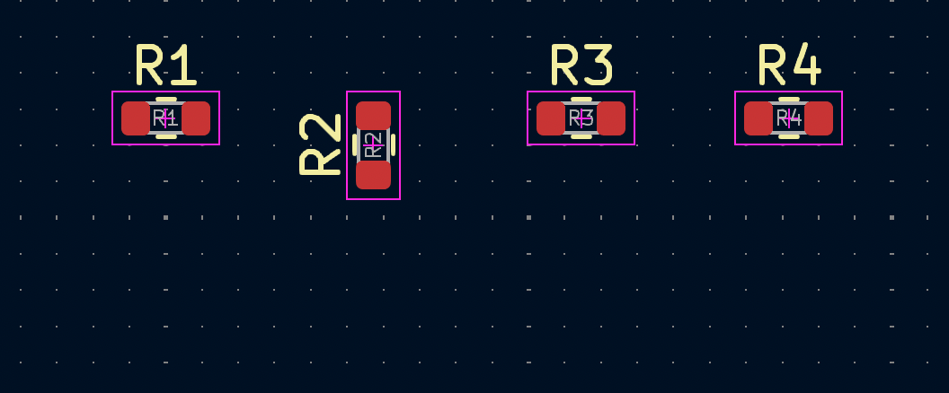
After alignment
In the example above, R1-R4 are vertically aligned by their top edges, with R2 as the reference object. The first image shows them before alignment and the second image shows them after alignment. In this case, R2 is the topmost object before alignment, so it is chosen as the reference object if the cursor is not over another resistor. After alignment, the top edges of the resistors are at the same position, but the horizontal positions of the resistors are unchanged.
Distributing objects
You can use the distribute tool to move objects so they are evenly spaced from each other (right click a selection → Align/Distribute → Distribute Horizontally or Distribute Vertically). The two outermost objects in the selection are not moved. This means the top and bottom objects when distributing vertically, and the leftmost and rightmost objects when distributing horizontally. The remaining objects in the selection are evenly distributed between the outermost objects and maintain their relative ordering. Objects are only moved in one dimension, so objects stay in the same horizontal position when distributed vertically, and vice versa.
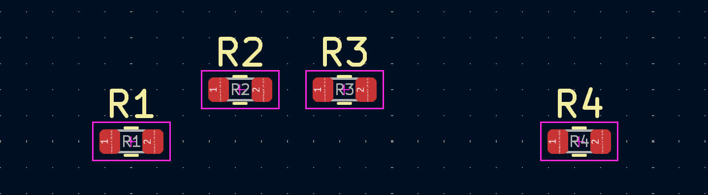
Before distribution
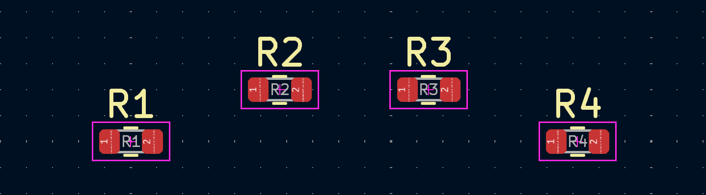
After distribution
In the example above, R1-R4 are horizontally distributed. The first image shows them before distribution and the second image shows them after distribution. R1 and R4 are the leftmost and rightmost objects, so they are not moved. R2 and R3 are moved so the horizontal spacing between resistors is equal, but the vertical positions remain unchanged. From left to right, R1-R4 are in the same order that they were in before distribution.
Arrays
KiCad has an array tool to create rectangular or circular arrays of objects (footprints, vias, graphical objects, etc.). To create an array, select the item(s) to be arrayed, right click, and choose Create from Selection → Array… (Ctrl+T).
There are two types of arrays, Grid (rectangular) and Circular.
Grid arrays
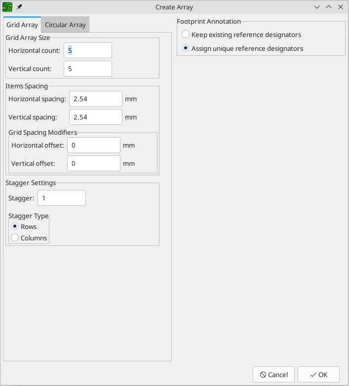
Grid Arrays are rectangular grids of rows and columns.
-
Horizontal count controls the number of columns in the array.
-
Vertical count controls the number of rows in the array.
-
Horizontal spacing controls the distance between columns.
-
Vertical spacing controls the distance between rows.
-
Horizontal offset applies a horizontal shift to each row compared to the previous row.
-
Vertical offset applies a vertical shift to each column compared to the previous column.
-
Stagger controls the number of rows or columns that are offset before the pattern repeats. You can stagger by Rows or by Columns. For example, if two staggered rows are selected, each row will be horizontally offset from the previous row by half of the array’s horizontal spacing setting. Every other row will be placed at the original spacing and offset. If three staggered columns are selected, each column will be vertically offset by a third of the array’s vertical spacing setting. Every third column will be placed at the original spacing and offset. Offsets from the stagger settings are added to the previous horizontal and vertical offset settings.
-
If the Grid Position option is set to Source items remain in place, the original items will not be moved, and the grid extends with those items at one corner. If Center on source items is chosen, the grid is offset so that the resulting grid is centered where the items used to be.
Circular arrays
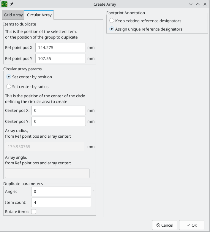
Circular Arrays are described by a center point, an angular spacing, and, optionally, the number of arrayed items.
-
Center pos X and Center pos Y define the absolute X/Y position of the center of the array. You can interactively set this location by selecting a point from the board using Select Point…, or by selecting the origin point of another item using Select Item….
-
The Item count field determines the number of objects in the array, including the source object.
-
The Angle between items field determines the angular spacing between items, with the center point at the center of the array.
-
When Full circle is selected, the array will always form a full circle, and therefore the angle between items will be automatically calculated based on the item count.
-
Clockwise/Anti-clockwise control the direction in which the arrayed items are positioned around the center point. If a negative spacing angle was entered, the array direction will be opposite of this setting (a negative angle combined with Anti-clockwise will result in a clockwise array).
-
When Rotate items is selected, objects will be rotated around their origins as array sweeps around the center point. Otherwise, objects will maintain the same orientation as the source item.
Common array options
The Item Source and Footprint Annotation settings apply to both types of arrays.
If Item Source is set to Duplicate selection, the array will be created by duplicating the selected items as necessary to fill out the configured array size. You should select this option if your board design does not yet contain all of the items that will make up the array, and you want the array tool to add those items as it creates the array. If this option is instead set to Arrange selection, no new items will be added to the board as the array is created. The array tool will create the array using only the items in your original selection. If you have not selected enough items to fill out the configured array size, the array will be incomplete after it is created.
When Duplicate selection is chosen, there is an additional Footprint Annotation option. This controls how reference designators will be set for new footprints that are added to the board by the array tool. This affects the linkage of the new footprints to the schematic. If Keep existing reference designators is selected, the new footprints in the array will have the same reference designators as the source footprints, resulting in duplicated reference designators in the board. If assign unique reference designators is selected, each new footprint created in the array will have a unique reference designator automatically assigned.
| Creating an array of footprints with the Duplicate selection option will result in multiple copies of the source footprint(s). If you are using a schematic-based workflow, this will result in footprints that are not represented in the schematic, so careful syncing between the board and the schematic will be needed. |
Using reference images
KiCad supports displaying reference images in the canvas. These are background images that you can use to help you lay out a board; they are purely for reference during the design process and are not included in any fabrication outputs.
To add a reference image, use the ![]() button on the right toolbar and browse to the desired reference image file. Click in the canvas to place the image.
button on the right toolbar and browse to the desired reference image file. Click in the canvas to place the image.
Once the image has been added to the canvas, you can reposition it using the move tool (M) or by dragging it in the canvas. The image is shown with five editing handles. Dragging one of the four handles at the image’s corners scales the image. The fifth corner is the image’s reference point; dragging the corner handles always scales the image around its reference point, with the reference point remaining stationary. You can move the reference point by dragging it to a new location. It is initially located in the center of the image, so the image scales equally in all directions from its center.
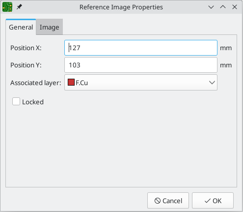
You can also reposition or resize the image in its properties dialog (E).
-
Position X controls the image’s exact X position.
-
Position Y controls the image’s exact Y position.
-
Associated layer controls the layer that the reference image is considered to be on. When a layer is hidden, any reference images on that layer are also hidden.
-
Height, Width, and Scale all control the size of the image in the board. Editing one of these properties causes the others to be updated proportionally. The proportions of the image are always maintained.
-
The Convert to Greyscale button changes the image from color to greyscale.
Reference images have an associated board layer; they are shown and hidden along with this layer. The layer initially associated with a reference image is the layer that was active when the image was added. You can change the associated layer in the image’s properties.
| Reference images are non-physical and are not included in any fabrication outputs, even when the image’s layer is plotted. |
Another way to hide reference images is with the Appearance Manager. You can show or hide all reference images by toggling the visibility of Image objects in the Objects tab (![]() button). You can also adjust the opacity of reference images here.
button). You can also adjust the opacity of reference images here.
Pin and gate swapping
KiCad has tools for pin and gate swapping, which let you quickly exchange nets between various footprint pads. These tools work either by swapping the nets assigned to individual pads in a footprint or by swapping the nets on all the pads that correspond to a symbol unit. Net connections are typically defined in the schematic, but pin and gate swapping work on the PCB: you edit the net connections in the PCB editor, then transfer the changes back to the schematic.
This type of modification is often identified during board layout, because the specific changes required often depend on particular details of the layout that are easier to see in the PCB Editor. Therefore, it can be very convenient to be able to easily swap net connections to pads.
| The tools described here are in the PCB Editor, and therefore work on footprint pads. However, any pad net changes will eventually be transferred back to the schematic, where the same edits will automatically be applied to the corresponding symbol pins. This section refers to pin swapping throughout, but understand that the pin and gate swap tools act directly on pads, not pins. Pin nets are not swapped until the schematic is updated from the PCB. |
Pin swapping exchanges the nets assigned to a selection of pins, so that the net that was assigned to one pin is moved to a different pin, and vice versa. For example, this could be used to swap the connections between two GPIO pins on a microcontroller.
Gate swapping is similar but works on all of the pins from a single symbol unit (the "gate"). All of the nets attached to one symbol unit’s pins are exchanged with the corresponding nets from another unit of the same symbol. For example, this could be used to swap between two opamp units in the same package, or two resistors in a resistor array.
Both types of swaps are explained in more detail below.
It’s important to understand that in KiCad, pin and gate swaps are unconstrained. This means that KiCad allows you to swap any pins or units; the tool does not check that the swapped pins are equivalent. As the designer, it is up to you to make sure that any swaps are valid, and you must ensure that all connections in the final design are correct.
When you perform a pin or gate swap in the PCB Editor, the board is updated immediately, as with any other board editing action. However, the schematic is not updated until you sync your changes to the Schematic Editor with Update Schematic From PCB.
Pin and gate swaps can also be performed in the Schematic Editor. In this case, the schematic is updated immediately, but the changes are not reflected in the PCB until they are synced using Update PCB From Schematic.
Pin swaps
Pin swapping exchanges the assigned nets between a selection of footprint pads. The pads must be part of the same footprint, but otherwise there are no restrictions on which pads can be used in a pin swap.
| It is up to you to ensure that the new pin connections are valid after a pin swap. |
In addition to swapping pad nets, pin swapping also swaps the nets on any tracks, vias, and other copper items connected to the pads. Connected zones keep their original nets. If there are additional pads that weren’t selected but were connected to the pads involved in the swap (for example, the pads of another connected component), KiCad will prompt and ask whether to also change the nets of those connected pads. You can choose to ignore the unselected pads, keeping their original nets, or to include all connected pads in the swap, even if they were not selected.
You can swap the nets between pads by selecting the pads, right clicking, and choosing Swap Pad Nets.
The example below shows a microcontroller, before and after a pin swap between GPIO pins 10 and 11. The nets of connected tracks were also swapped, as were the nets of the connected pads of the LEDs on the left.
Before swapping pins 10 and 11
After swapping pins 10 and 11
Gate (unit) swaps
Gate swaps exchange the connections between two or more units of the same multi-unit symbol. In this context, gate refers to a symbol unit.
Symbol units can only be swapped if they meet the following conditions:
-
They are part of the same symbol.
-
They have the same number of pins.
When you perform a gate swap, the pads corresponding to one symbol unit have their nets swapped with the pads from another symbol unit. Pins are matched from one unit to another by their location in the symbol, so a pin in one unit is considered equivalent to a pin in another unit if they are in the same location in each unit.
Nets are also swapped for tracks, vias, and other copper items connected to the pads. Connected zones keep their original nets. If there are additional pads that weren’t selected but were connected to the pads involved in the swap (for example, the pads of another connected component), KiCad will prompt and ask whether to also change the nets of those connected pads. You can choose to ignore the unselected pads, keeping their original nets, or to include all connected pads in the swap, even if they were not selected.
You can perform a gate swap in two ways:
-
Select one or more pads from the same symbol unit, right click, and choose the target symbol unit from the Swap Gate Nets submenu. The selected pads, as well as all other pads from the same symbol unit, will have their nets swapped with the corresponding symbol pins from the target unit.
-
Select two or more pads from different symbol units, right click, and choose Swap Gate Nets. The nets from the first pad’s symbol unit are swapped with the corresponding nets from the second pad’s unit.
The example below shows a dual op-amp, before and after a gate swap between units A and B. The nets of connected tracks were also swapped, as were the nets of the connected pads of the surrounding resistors.
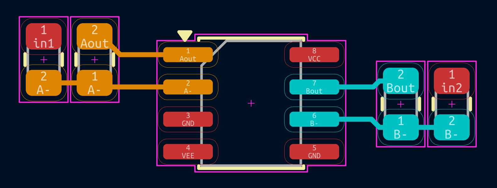
Before swapping units A and B
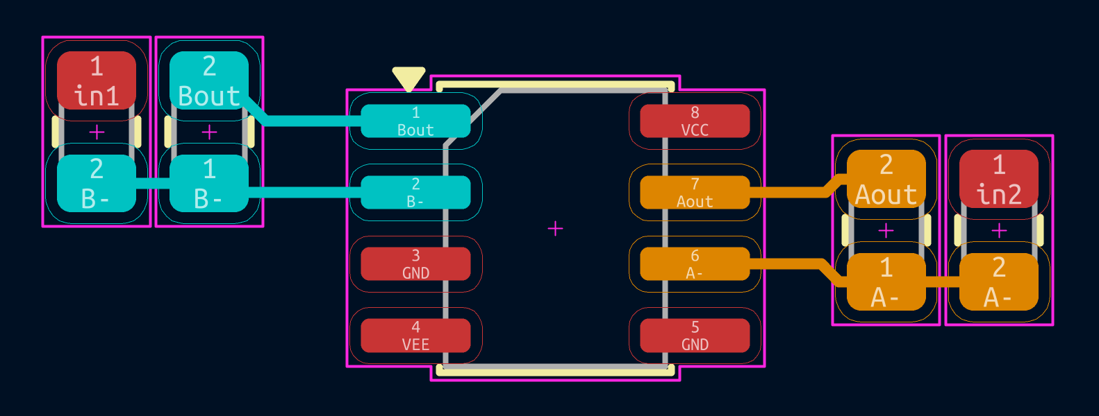
After swapping units A and B
Swapping more than two items
When a swap is performed on two items (pins or gates), one item is exchanged with the other in a one-for-one swap. But when a swap is performed on three or more items, the items are cycled in the order they were selected. The first-selected item replaces the second-selected item, the second item replaces the third, and so on. The last-selected item replaces the first item.
When swapping pins, this means the net from the first-selected pad is transferred to the second-selected pad, the second pad’s net is transferred to the third, etc. When swapping gates, the nets from the first-selected pad’s unit are transferred to the pads from the second unit, etc.
Syncing pin and gate swaps to the schematic
When you perform a pin or gate swap, the pad nets are immediately swapped in the PCB. However, the schematic is not updated until you back-annotate the changes using the Update Schematic from PCB tool.
There are three back-annotation options that are especially important when syncing pin and gate swaps:
- Net Names
-
This option needs to be enabled in order to sync pin and gate swaps back to the schematic.
- Prefer symbol unit swaps over label swaps
-
This option controls how PCB gate swaps change the schematic.
If it is enabled, gate swaps will be transferred to the schematic by swapping the position of each symbol unit. This mode should be preferred when there are other symbols directly connected to the symbol units in the schematic, as gate swaps with these topologies cannot be represented by net label swaps.
If it is disabled, gate swaps will be represented in the schematic by swapping net labels while keeping the symbol units in their original positions. This mode is useful if nets are attached to the symbol units using net labels.
- Prefer symbol pin swaps over label swaps
-
This option controls how PCB pin swaps change the schematic.
If it is enabled, pin swaps will be transferred to the schematic by swapping pins in the symbol. This modifies the schematic copy of the symbol.
Symbol pins can only be swapped if the Allow unconstrained pin swaps option is enabled in the Editing Options page of the Schematic Editor’s preferences. If it is disabled, pin swaps will be represented in the schematic by swapping labels rather than modifying symbols.
向前和向后批注
Forward and back annotation are the processes for syncing schematic changes to the board and syncing board changes to the schematic, respectively.
从原理图更新 PCB(正向批注)
使用 "从原理图更新 PCB" 工具将设计信息从原理图编辑器同步到电路板编辑器。在原理图编辑器和电路板编辑器中都可以用 工具 → 从原理图更新 PCB(F8)来访问该工具。你也可以使用电路板编辑器顶部工具栏上的 ![]() 图标。这个过程通常被称为正向批注。
图标。这个过程通常被称为正向批注。
| 从原理图更新 PCB 是将设计信息从原理图转移到 PCB 的首选方法。在旧版本的 KiCad 中,相应的过程是将网表从原理图编辑器中导出并导入到电路板编辑器中。现在已经没有必要使用网表文件了。 |
该工具将每个符号的封装添加到电路板上,并将更新的原理图信息传输到电路板上。尤其重要的是,电路板的网络连接也将更新以匹配原理图。
将对 PCB 进行的变更列在 待应用的变更 窗格中。在你点击 更新 PCB 按钮之前,PCB 不会被修改。
你可以使用窗口底部的复选框来显示或隐藏不同类型的信息。可以使用 保存… 按钮将变更的报告保存到文件中。
选项
该工具有几个选项来控制其行为。
| Option | Description |
|---|---|
Re-link footprints to schematic symbols based on their reference designators |
Footprints are normally linked to schematic symbols via a unique identifier created when the symbol is added to the schematic. A symbol’s unique identifier cannot be changed, but will be lost when the symbol is deleted, even if a symbol with the same reference designator replaces it. If checked, each footprint in the PCB will be re-linked such that each footprint has its unique identifier updated to match the symbol that has the same reference designator as the footprint. This option should generally be left unchecked. See below for more details on when to use this option. |
Group footprints based on symbol group |
If checked, footprints will be added to groups in the PCB if their linked symbols are grouped. |
Replace footprints with those specified by symbols |
If checked, footprints in the PCB will be replaced with the footprint that is specified in the corresponding schematic symbol. If unchecked, footprints that are already in the PCB will not be changed, even if the schematic symbol is updated to specify a different footprint. |
Delete footprints with no symbols |
If checked, any footprint in the PCB without a corresponding symbol in the schematic will be deleted from the PCB. Footprints with the "Not in schematic" attribute will be unaffected. If unchecked, footprints without a corresponding symbol will not be deleted. |
Override locks |
If checked, locking a footprint will not affect whether a footprint is deleted or replaced based on changes in the schematic. If unchecked, locked footprints will never be deleted or replaced even if they otherwise would be. |
Update footprint fields from symbols |
If checked, new and updated fields in symbols will be transferred to the corresponding footprints, keeping symbol and footprint fields in sync. If unchecked, footprint fields will not be updated when fields change in the corresponding symbols. |
Remove footprint fields not found in symbols |
If checked, footprint fields will be removed if they do not exist in the corresponding symbol. If unchecked, footprint fields that do not exist in the corresponding symbol will not be removed, allowing footprints to have additional fields compared to the corresponding symbols. |
Re-linking symbols and footprints
Symbols and footprints are linked together using unique identifiers (also called UUIDs). These are handled automatically within KiCad and are not usually visible to users. They allow a symbol and its partner footprint to keep their connection between schematic and PCB, even if the reference designator is changed. New objects get assigned their identifiers upon creation.
Re-linking by unique identifier (default)
In normal use, the Re-link footprints to schematic symbols based on their reference designators option should be unchecked. In this mode, symbols with the same identifier as a footprint will update that footprint, regardless of the reference designator. Symbols which have an identifier that doesn’t match any footprint will add a new footprint linked to that identifier.
For example, in the below schematic, both R1 and R2 are linked via their unique IDs to footprints on the PCB:
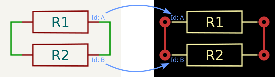
If symbol reference designators are changed in the schematic (e.g. by re-annotation), running the Update PCB from Schematic process will update the reference designators on the PCB.
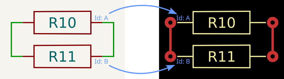
Re-linking by reference designator
If the checkbox is checked, the linking process is done using the reference designators. This can be useful for workflows that result in a symbol being deleted and replaced by another one, rather than being updated in-place. For example, cut-and-pasting a block of schematic or a sheet and copy-pasting and re-annotating will usually break the identifier-based links.
For example in the below case, the resistors R1 and R2 have been deleted and replaced, then re-annotated. While the reference designators are the same, the internal identifiers have changed. Updating the PCB by identifier would cause the existing footprints to be deleted and new ones added - to KiCad, the existing footprints have no matching symbol. This would cause the footprints to lose their positions and need placing again.
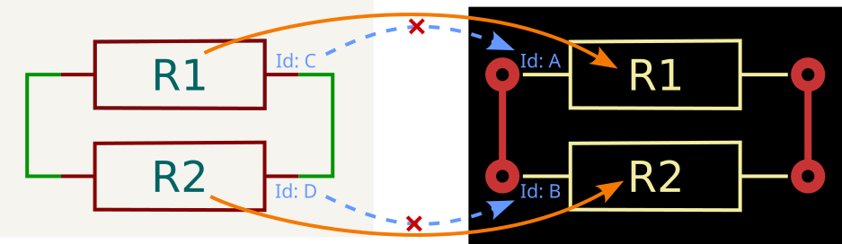
Re-linking the footprints by reference designator causes KiCad to re-create the links, using the matching reference designators as a guide.
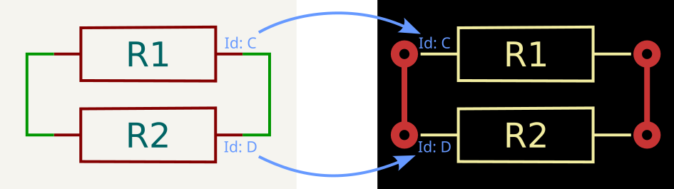
Because the links have been re-established, the next forward annotation should use the normal identifier-based linking (i.e. the checkbox should be unchecked).
从 PCB 更新原理图(反向批注)。
KiCad 的典型工作流程是在原理图中进行修改,然后使用 "从原理图更新 PCB" 工具将修改内容同步到电路板上。然而,相反的过程也是可行的:可以在电路板上进行设计修改,然后在原理图或电路板编辑器中使用 工具 → 从 PCB 更新原理图 同步到原理图上。这个过程通常被称为反向批注。
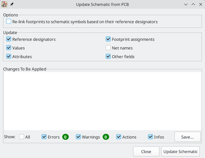
The tool syncs changes in reference designators, values, attributes (like DNP or Exclude From BOM), footprint assignments, other fields, and net names from the board to the schematic. Each type of change can be individually enabled or disabled.
将对原理图进行的变更列在 待应用的变更 窗格中。在您点击 更新原理图 按钮之前,原理图不会被修改。
你可以使用窗口底部的复选框来显示或隐藏不同类型的信息。可以使用 保存… 按钮将变更的报告保存到文件中。
选项
该工具有几个选项来控制其行为。
Option |
Description |
Re-link footprints to schematic symbols based on their reference designators |
If checked, each footprint in the PCB will be re-linked to the symbol that has the same reference designator as the footprint. This option is incompatible with updating symbol reference designators. If unchecked, footprints and symbols will be linked by unique identifier as usual, rather than by reference designator. This option should generally be left unchecked. See above for more details on when to use this option. |
Reference designators |
If checked, symbol reference designators will be updated to match the reference designators of the linked footprints. If unchecked, symbol reference designators will not be updated. |
Values |
If checked, symbol values will be updated to match the values of the linked footprints. If unchecked, symbol values will not be updated. |
Attributes |
If checked, symbol attributes (like exclude from BOM and DNP) will be updated to match the corresponding attributes of the linked footprints. If unchecked, symbol attributes will not be updated. |
Other fields |
If checked, other symbol fields will be updated to match the corresponding fields of the linked footprints. Reference designator, value, and footprint are each controlled by their own separate option. If unchecked, other fields will not be updated in the schematic. |
Footprint assignments |
If checked, footprint assignments will be updated for symbols which have had their footprints changed or replaced in the board. If unchecked, symbol footprint assignments will not be updated. |
Net names |
If checked, the schematic will be updated with any net name changes that have been made in the board. Net labels will be updated or added to the schematic as necessary to match the board. If unchecked, net names will not be updated in the schematic. |
Prefer symbol unit swaps over label swaps |
The tool will detect situations where net connections within a multi-unit symbol have changed due to entire symbol units (gates) being swapped. Such swaps will be detected whether they were performed using the gate swap tool or whether the equivalent net changes were made manually. If checked, in these situations the schematic will be updated to match the PCB by swapping symbol units rather than swapping the net labels attached to the pins on each symbol unit. If unchecked, symbol unit swaps will be represented in the schematic by swapping net labels rather than swapping symbol units. |
Prefer symbol pin swaps over label swaps |
The tool will detect situations where net connections have swapped between two pins within a symbol. Such swaps will be detected whether they were performed using the pin swap tool or whether the equivalent net changes were made manually. If checked, in these situations the schematic will be updated to match the PCB by swapping symbol pins in the symbol rather than swapping the net labels attached to the pins, if possible. Symbol pins can only be swapped if the Allow unconstrained pin swaps option is enabled in the Editing Options page of the Schematic Editor’s preferences. If unchecked, symbol pin swaps will be represented in the schematic by swapping net labels rather than swapping pins in the symbol. |
| 按位置重新批注 功能可以与反向批注位号结合使用,根据设计中的位置重新批注所有元件。 |
用 CMP 文件进行反向批注
通过从 PCB 编辑器导出 CMP 文件(文件 → 导出 → 封装关联(.cmp)文件…)并在原理图编辑器中导入(文件 → 导入 → 封装分配…),也可以将选择的变化从 PCB 上同步到原理图。
| 这种方法只能同步对封装分配和封装字段的修改。建议使用 "从 PCB 更新原理图" 工具来代替。 |
按位置重新批注
The Geographical Reannotation tool lets you automatically set the reference designators of footprints based on their physical location on the board.
To run the Geographical Reannotation tool, use Tools → Geographical Reannotate…. This opens the geographical reannotation dialog with options for how to perform the reannotation.
- Footprint Order
-
This section contains settings for how footprint locations affect reannotation.
The arrow diagrams indicate which geographical ordering to use when reannotating. You can reannotate from left-to-right, right-to-left, top-to-bottom, or bottom-to-top, and you can select whether to use a column-major order (go through all footprints in the same column before moving to the next column) or row-major order (go through all footprints in the same row before moving to the next row).
Geographical reannotation can either use the location of the footprint itself or the location of the footprint’s reference designator. You can also select how much to round footprint locations before determining which footprints are at the same X or Y position. Rounding to a finer coordinate resolution will result in fewer footprints considered to be in the same row or column.
- Reannotation Scope
-
This section controls which footprints to reannotate. You can reannotate all footprints on the board, all footprints on the front or back of the board, or all footprints in your selection.
If Exclude locked footprints is checked, locked footprints will not be reannotated. You can also avoid reannotating specific footprints by entering their reference designators as a comma-separated list in the Exclude references box.
- Reference Designators
-
This section contains options for how to allocate new reference designators. There are separate settings for footprints on the front and back of the board.
Front reference start controls the number for the first new reference designator on the front side of the board. Back reference start controls the first number on the back of the board. If no start value is given for the back of the board, back side footprints will be annotated starting at one higher than the last front side reference designator.
Front prefix specifies a prefix string to insert at the beginning of each newly assigned reference designator on the front of the board. Back prefix controls the prefix for footprints on the back of the board. This prefix will be inserted before any prefix that is already present. If the Remove front prefix or Remove back prefix options are selected, footprints with the specified prefix will instead have that prefix removed instead of added. Footprints without that prefix will not have not have any prefix added or removed.
When you click the Reannotate PCB button, footprints will be reannotated according to the selected settings.
| The Geographical Reannotation tool updates reference designators in the board, but not in the schematic. After geographically reannotating the board, be sure to sync the updated reference designators to the schematic by running the Update Schematic from PCB tool with the re-link footprints to schematic symbols based on their reference designators option disabled. If the schematic is not updated, reference designators in the board will not match those in the schematic. |
检查电路板
Design rules checking
The Design Rules Checker (DRC) tool is used to verify that the PCB meets all the requirements established in the Board Setup dialog and that all pads are connected according to the netlist or schematic. KiCad can automatically prevent some design rule violations while routing tracks, but many others cannot be prevented automatically. This means it is important to use the design rule checker before creating manufacturing files for a PCB.
要使用设计规则检查器,请点击顶部工具栏的 ![]() 图标,或从 检查 菜单中选择 设计规则检查器。
图标,或从 检查 菜单中选择 设计规则检查器。
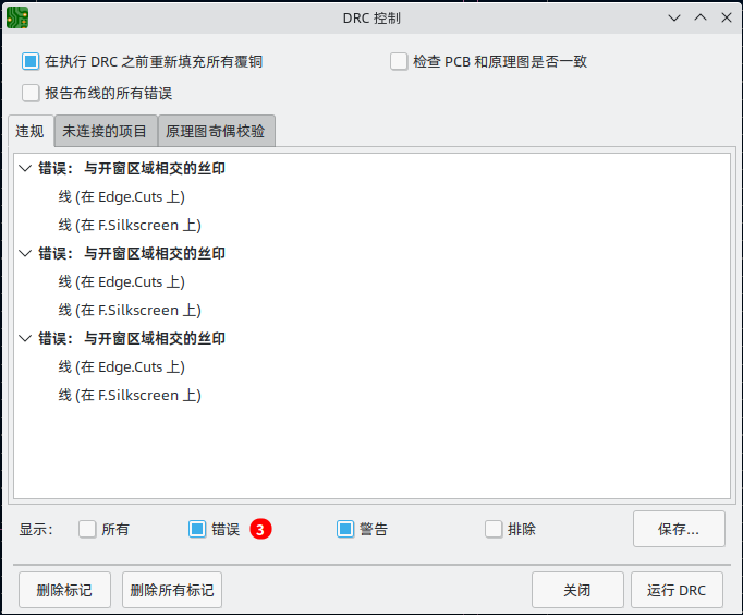
DRC 控制窗口的顶部部分包含一些控制设计规则检查器的选项:
- Refill all zones before performing DRC
-
When enabled, zones will be refilled every time the design rule checker is run. Disabling this option may result in incorrect DRC results if zones have not been refilled manually.
- Test for parity between PCB and schematic
-
When enabled, the design rule checker will test for differences between the schematic and PCB in addition to testing the PCB design rules. This option has no effect when running the PCB editor in standalone mode.
Several additional options are in the ![]() menu.
menu.
- Report all errors for each track
-
When enabled, all clearance errors will be reported for each track segment. When disabled, only the first error will be reported. Enabling this option will result in the design rule checker running more slowly.
- Cross-probe Selected Items
-
When enabled, selecting an item or a violation in the DRC window will move the cursor to that item in the editing canvas.
- Center on Cross-probe
-
When enabled, selecting an item or a violation in the DRC window will center the editing canvas on the item or violation marker. This option has no effect if the Cross-probe Selected Items option is disabled. Note that if the Center view on cross-probed items option is enabled in the PCB Editor’s Display Options section of preferences, cross-probed objects will be centered even if this option is disabled.
After running DRC, any violations will be shown in the center part of the DRC window. Rule violations, unconnected items, and differences between the schematic and the PCB are shown in three different tabs. A list of the ignored tests is shown in the fourth tab. A report file in plain text format can be created after running DRC using the Save… button.
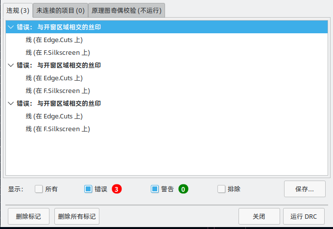
Each violation involves one or more objects on the PCB. In the list of violations, the objects involved are listed below the violation. Depending on your settings, clicking on the violation in the list view will move the PCB Editor view so that the affected area is centered. Clicking on one of the objects involved in a violation will highlight the object.
Many types of violations have contextual actions in the context menu. For example, clearance violations have an action to run the clearance resolution tool on the violating items, while custom rule violations have an action to run the constraint resolution tool. For board vs. library footprint mismatch violations, there is an action to run the Compare Footprint with Library tool and another action to update the footprint from the library. These actions can help to quickly fix identify the reason for a particular violation.
The numbers at the bottom of the window show the number of errors, warnings, and exclusions. Each type of violation can be filtered from the list using the respective checkboxes. Clicking Delete Marker will clear the selected violation until DRC is run again, while clicking Delete All Markers will clear all violations until the next DRC run.
可以在对话框中右键单击违规行为,以忽略它们或改变其严重程度:
-
Exclude this violation: ignores this particular violation, but does not affect any other violations. You can un-exclude a violation by right clicking the excluded violation and selecting Remove exclusion for this violation.
-
Exclude with comment…: the same as Exclude this violation, but prompts for a comment explaining the reason for the exclusion. When excluded violations are unhidden (using the Exclusions checkbox), exclusion comments are shown with the corresponding excluded violation. To edit an existing exclusion comment or add a comment to an existing exclusion, right click an excluded violation and select Edit exclusion comment….
-
Exclude all violations of rule: the same as Exclude this violation, but excludes all violations caused by the same custom DRC rule. This action only appears in the context menu for violations caused by custom design rules. If you right click on a custom design rule violation that is already excluded, you can instead Remove all exclusions for violations of rule.
-
Change severity: changes a type of violation from warning to error, or error to warning. This affects all violations of a given type.
-
Ignore all: ignores all violations of a given type. This test will now appear in the Ignored Tests tab rather than the Violations tab. You can un-ignore the test again by right clicking the test in the Ignored Tests tab, or in the Violation Severity panel in Board Setup.
-
Edit violation severities…: opens the Violation Severity panel in Board Setup, for editing the severities of all DRC violation types.
Excluded and ignored violations are remembered between runs of the design rule checker. Excluded violations are hidden unless the Exclusions checkbox is enabled. Ignored violations are not shown, but there is a list of ignored tests in the Ignored Tests tab.
间隙和约束解析
间隙和约束解析工具允许你检查哪些间隙和设计约束规则应用于选定的项目。 当设计具有复杂设计规则的 PCB 时,这些工具可以提供帮助,因为在这种情况下并不总是清楚哪些规则适用于哪些对象。
To inspect the clearance rules that apply between two objects, select both objects and choose Clearance Resolution from the Inspect menu. If you haven’t selected two objects, you are prompted to pick them. The Clearance Report dialog will show the clearance required between the objects on each copper layer, as well as the design rules that resulted in that clearance. It can also inspect hole clearances (the clearance between a hole and another object or hole) and physical clearances (the clearance between any two objects, whether copper or not).
| If you don’t select two items before running the Clearance Resolution tool, you are prompted to pick two items interactively. This can be useful to check the clearance between two items that would otherwise be difficult to select at the same time, such as items in two different groups. |
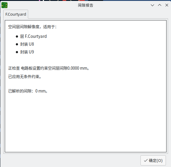
To inspect the design constraints that apply to an object, select it and choose Constraints Resolution from the Inspect menu. If you haven’t selected an object, you are prompted to pick one. The Constraints Report dialog will show any constraints that apply to the object.
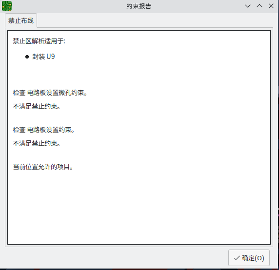
DRC configuration
The severity of each DRC check can be configured in the Violation Severity section of the Board Setup dialog. Each rule may be set to create an error marker, a warning marker, or no marker (ignored).
| 在设计规则检查器中可能会忽略个别规则违规。 在违规程度部分中将规则设置为忽略将完全禁用相应的设计规则检查。 请谨慎使用此设置。 |
List of DRC checks
The table below lists the design rules that KiCad checks and the default violation severity for each check. All severities are configurable. Some design are only available through custom design rules.
Electrical DRC checks
These DRC checks look for gross electrical issues on the board such as shorts and clearance violations.
| Violation | Description | Default Severity |
|---|---|---|
Items shorting two nets |
This violation occurs when copper items on different nets collide with each other. If this is intentional, consider using a net tie. |
Error |
Tracks crossing |
This violation occurs when tracks with different nets cross each other. |
Error |
Clearance violation |
This violation occurs when the distance between two copper items with different nets is smaller than the configured clearance for those nets. The allowed clearance between two items can come from the board-level minimum clearance, the net class settings for each net, or from custom rules. To see detailed information about the configured and actual clearances between two selected items, run the clearance resolution tool, which is available by right clicking the violation in the DRC window. The minimum clearance path is highlighted in the editing canvas when a clearance violation is selected in the DRC window. This violation is also reported when the distance between two items is smaller than the configured physical clearance for those two items. Physical clearance constraints are not configured by default; see the custom rule documentation for how to configure physical clearance. |
Error |
Creepage violation |
This violation occurs when the creepage distance between two copper items with different nets is smaller than the configured creepage for those nets. Creepage paths are highlighted in the editing canvas when a creepage violation is selected in the DRC window. Creepage distances can be configured using a |
Error |
Via is not connected or is connected on only one layer |
This violation occurs when a via is connected to copper objects on only one layer or is not connected to anything. As vias are intended to connect copper objects on different layers, this may indicate that an intended connection is missing. |
Warning |
Track has unconnected end |
This violation occurs when the end of a track segment is not connected to another copper object, such as another track segment, a via or pad, or a zone or copper graphical shape. |
Warning |
Thermal relief connection to zone incomplete |
This violation occurs when a pad’s connection to a zone does not have enough connected thermal relief spokes. The minimum allowed number of spokes can come from the board-level minimum thermal relief spoke count or can be configured with more granularity using custom rules. This check counts automatically generated spokes as well as manually drawn connections, so if the pad and zone geometry prevent enough spokes from being generated, you can manually add additional connections using tracks or other copper shapes between the pad and the zone. |
Error |
Design for manufacturing DRC checks
These DRC checks look for issues in the board that may cause manufacturing problems.
| Violation | Description | Default Severity |
|---|---|---|
Board edge clearance violation |
This violation occurs when the distance between a copper object and the
board edge is smaller than the configured copper to edge clearance for those
items. For the purposes of this check, oval holes (which are routed rather
than drilled) are counted as board edges in addition to any graphic items
on the The allowed edge clearance between two items can come from the board-level minimum copper to edge clearance or from custom rules. A negative edge clearance allows objects to overlap with the board edge. To see detailed information about the configured and actual edge clearances between two selected items, run the clearance resolution tool. |
Error |
Hole clearance violation |
This violation occurs when the distance between a hole (pad or via) and another copper object (pad, track, via, or zone) is smaller than the configured copper to hole clearance for those objects. Objects are only considered in this check if they have layers in common. The allowed hole clearance between two items can come from the board-level minimum copper to hole clearance or from custom rules. To see detailed information about the configured and actual hole clearances between two selected items, run the clearance resolution tool. This violation is also reported when the distance between a hole and another object is smaller than the configured physical hole clearance for those two items. Physical hole clearance constraints are not configured by default; see the custom rule documentation for how to configure physical hole clearance. |
Error |
Drilled hole too close to other hole |
This violation occurs when the distance between a drilled hole and another hole is smaller than the configured hole to hole clearance. Through vias, blind and buried vias, and through holes in pads are considered drilled holes because the holes are made with a physical drill bit, which can shift or be damaged if other holes (drilled or otherwise) are too close. Micro vias are not considered drilled holes because they are drilled using a laser, which is not affected by other nearby holes. At least one of the holes must be mechanically drilled in order to be considered in this check. Blind and buried vias are only considered in this check when they share layers with the other hole. Non-circular holes are not included in this check because they are routed rather than drilled. Routing is typically performed after holes are drilled and with a stronger tool. |
Error |
Drilled holes co-located |
This violation occurs when a drilled hole and another hole are in the exact same location. The same types of holes are considered in this check as for the "Drilled hole too close to other hole" check. |
Warning |
布线宽度 |
This violation occurs when the width of a track is outside of the configured range. The allowed width for a track can come from the board-level minimum track width or from custom rules. Note that an optimal track width can be configured for each net class in the net class settings, which sets a track width for the interactive router to use, but it does not set a minimum and maximum track width. No DRC violations will be reported for net class track width settings unless a minimum and/or maximum are configured using custom rules. To see detailed information about the configured track width for a particular track, run the constraints resolution tool. |
Error |
Track angle |
This violation occurs when the angle between two connected track segments is outside the configured range. Minimum and/or maximum allowable track angles can be configured using a
|
Error |
Track segment length |
This violation occurs when the length of a track segment is outside the configured range. Minimum and/or maximum allowable track segment lengths can be configured
using a |
Error |
Annular width |
This violation occurs when a pad or via’s annular width is outside of the configured range. Board-level minimum annular width can be configured in board setup constraints. Board-level maximum width, as well as more specific rules, can be configured using custom rules. |
Error |
Hole size out of range |
This violation occurs when a drilled hole’s diameter is outside of the configured range. This check represents the smallest hole that can be drilled, i.e. the smallest drill bit size the manufacturer will use. This check therefore includes through vias, blind and buried vias, and through holes in pads. Micro vias are not included in this check because they are made using a laser rather than a physical drill bit. Board-level minimum through hole size can be configured in board setup constraints. Board-level maximum hole size, as well as more specific rules, can be configured using custom rules. |
Error |
Micro via hole size out of range |
This violation occurs when a micro via’s hole diameter is outside of the configured range. This check represents the smallest hole that can be laser drilled and therefore only applies to micro vias. Board-level minimum micro via hole size can be configured in board setup constraints. Board-level maximum hole size, as well as more specific rules, can be configured using custom rules. |
Error |
Courtyards overlap |
This violation occurs when a footprint’s courtyard overlaps with another
footprint’s courtyard. A nonzero clearance between two courtyards can be
configured using a |
Error |
Footprint has no courtyard defined |
This violation occurs when a footprint does not contain any graphic
shapes on its |
Ignore |
Footprint has malformed courtyard |
This violation occurs when a footprint has a courtyard containing non-closed shapes. Courtyards may contain multiple unconnected shapes without being considered malformed, as long as each shape is individually closed. |
Error |
Board has malformed outline |
This violation occurs when the shapes on the |
Error |
Copper sliver |
This violation occurs when small, wedge-shaped protrusions of copper are detected. These slivers can cause manufacturing, reliability, or electrical issues. |
Warning |
Solder mask aperture bridges items with different nets |
This violation occurs when a single opening in the soldermask exposes multiple copper items with different nets. This can result in solder shorting the two copper items during assembly. |
Error |
Copper connection too narrow |
This violation occurs when a copper connection necks down to a width that is narrower than the configured minimum connection width. The minimum connection width setting can come from the board-level minimum connection width or can be configured with more granularity using custom rules. |
Warning |
Track connected to post-machined or backdrilled layer |
This violation occurs when a track connects to a pad or via on a layer that has been removed from the pad/via by post-machining or backdrilling. |
Error |
Track endpoint not centered on via |
This violation occurs when a track’s endpoint lies within a via but not exactly at the via center. The length tuner will not report an accurate length for a track connecting to a via outside of the via’s center. |
Warning |
Tuning profile track geometries |
This violation occurs when a track’s geometry (track width or differential pair gap) do not match the values from the track’s tuning profile. |
Ignore |
Schematic parity DRC checks
These DRC checks look for differences between the schematic and the board.
| Violation | Description | Default Severity |
|---|---|---|
Duplicate footprints |
This violation occurs when the board contains multiple footprints with the same reference designator are in the board. It is not reported if the footprints do not correspond to schematic symbols, however (if the footprints only exist in the board). |
Warning |
Missing footprint |
This violation occurs when a footprint is not in the board but is expected based on a corresponding symbol in the schematic. |
Warning |
Extra footprint |
This violation occurs when a footprint is in the board without a corresponding symbol in the schematic. |
Warning |
Footprint attributes don’t match symbol |
This violation occurs when a footprint’s Typically this is fixed by performing an Update PCB from Schematic or Update Schematic from PCB action to sync the fields and attributes, depending on whether the symbol or footprint, respectively, is correct. |
Warning |
Footprint doesn’t match symbol’s footprint filters |
This violation occurs when a footprint does not match footprint filters in the corresponding symbol. If the symbol doesn’t have any footprint filters, no violation occurs. |
Ignore |
Pad net doesn’t match schematic |
This violation occurs when a net does not match between a footprint pad and the corresponding symbol pin. This can be because the symbol pin’s net is different than the footprint pad’s net, because the footprint pad does not have a corresponding symbol pin, or because the symbol pin does not have a corresponding footprint pad. |
Warning |
Missing connection between items |
This violation occurs when two copper objects with the same net are not connected on the board. |
Error |
Signal integrity DRC checks
These DRC checks look for signal integrity issues in the board.
| Violation | Description | Default Severity |
|---|---|---|
Track length out of range |
This violation occurs when a track in a differential pair is too long or too
short compared to the configured minimum and maximum length for that track.
The allowable track length for different tracks can be configured using the
|
Error |
Skew between tracks out of range |
This violation occurs when the difference between the length of a track and the maximum length of all tracks being considered is longer than the configured maximum skew for that set of tracks. For calculating the skew of a differential pair (two tracks), the skew therefore is calculated as the length difference between tracks. The allowable maximum skew for a set of tracks, as well as which tracks the
rule applies to, can be configured using the |
Error |
Too many or too few vias on a connection |
This violation occurs when the number of vias assigned to a net is too low
or too high compared to the configured minimum and maximum for that net. The
allowable via count for different nets can be configured using the
|
Error |
Differential pair gap out of range |
This violation occurs when the gap between the two tracks in a differential pair is too small or too large compared to the configured minimum and maximum for that differential pair. The gap is only checked on coupled (i.e. parallel) portions of the differential pair. The minimum and maximum allowable gap for a differential pair can be
configured using the Note that an optimal differential pair gap can be configured for each net class in the net class settings, which sets a gap for the differential pair router to use, but it does not set a minimum and maximum gap. No DRC violations will be reported unless a minimum and/or maximum are configured using custom rules. |
Error |
Differential uncoupled length too long |
This violation occurs when the portion of a differential pair that is uncoupled is longer than the configured maximum. A differential pair is considered uncoupled when its tracks are not parallel, for example when fanning out from a footprint. The maximum allowable uncoupled length for a differential pair can be
configured using the |
Error |
Readability DRC checks
These DRC checks look for issues that may affect legibility of text and other silkscreen objects on the board.
| Violation | Description | Default Severity |
|---|---|---|
Silkscreen clearance |
This violation occurs when a silkscreen object intersects another silkscreen object, which may affect readability. Collisions that only involve shapes are not reported; for example, the intersection of two silkscreen lines doesn’t cause a violation, but a line intersecting a text object does. The allowable distance between silkscreen objects can be set to a
nonzero number to enforce a silk to silk clearance using the
board-level silkscreen minimum item clearance or
using custom rules with the A negative silkscreen clearance allows silkscreen to intersect other objects. |
Warning |
Silkscreen clipped by solder mask |
This violation occurs when a silkscreen object intersects a solder mask opening. This may result in silkscreen printed on bare copper or substrate. Board manufacturers may also discard any silkscreen that does not have solder mask underneath. Such outcomes could affect board assembly as well as silkscreen durability and readability. |
Warning |
Silkscreen clipped by board edge |
This violation occurs when a silkscreen object intersects a board edge, meaning that part of the silkscreen is outside of the board area. The allowable distance between silkscreen and the board edge can also be set
to a nonzero number to enforce a clearance to the board edge using the
board-level silkscreen minimum item clearance or
using custom rules with the |
Warning |
Text height out of range |
This violation occurs when a text object’s text height is outside of the configured range. Board-level minimum text height can be configured in board setup constraints. Board-level maximum height, as well as more specific rules, can be configured using custom rules. |
Warning |
Text thickness out of range |
This violation occurs when a text object’s text thickness is outside of the configured range. For the built-in KiCad stroke font, the thickness is the text thickness setting in the text object’s properties. For external fonts, this is the minimum physical thickness of all glyphs in the text object; this depends on the font geometry in combination with the font size, bold, and italic settings. Board-level minimum text thickness can be configured in board setup constraints. Board-level maximum thickness, as well as more specific rules, can be configured using custom rules. |
Warning |
Mirrored text on front layer |
This violation occurs when a text object on a front layer has the mirrored attribute set. When looking at the front of the board, the text will therefore appear backwards. |
Ignore |
Non-Mirrored text on back layer |
This violation occurs when a text object on a back layer doesn’t have the mirrored attribute set. When looking at the back of the board, the text will therefore appear backwards. |
Ignore |
Miscellaneous DRC checks
These DRC checks look for other miscellaneous issues in the board.
| Violation | Description | Default Severity |
|---|---|---|
Items not allowed |
This violation occurs when objects are placed in a location where they are
not allowed. This can be due to a rule area with a keep
out rule for the object’s type or due to a |
Error |
Copper zones intersect |
This violation occurs when copper zones with different nets collide with each other, shorting the two nets. |
Error |
Isolated copper fill |
This violation occurs when part of a copper fill is not connected to any other copper items with the same net. This is also referred to as an island. |
Warning |
Footprint is not valid |
This violation occurs when a footprint’s net tie group contains a pad that doesn’t exist in the footprint, or when a pad is in more than one net tie group. |
Error |
Padstack is questionable |
This violation occurs when a footprint pad has unusual settings that are probably a mistake. The settings that are checked are:
|
Warning |
PTH inside courtyard |
This violation occurs if a footprint’s plated through hole pad is within the courtyard of another footprint. Pads with the "heatsink pad" fabrication property are allowed, however. |
Error |
NPTH inside courtyard |
This violation occurs if a footprint’s nonplated through hole pad is within the courtyard of another footprint. |
Error |
Item on a disabled copper layer |
This violation occurs if an item, for example a pad or via, is on a copper layer that does not exist in the board stackup. |
Error |
Unresolved text variable |
This violation occurs when a text variable in the board design or drawing sheet does not resolve (there is no defined value for the variable). |
Error |
Footprint component type doesn’t match footprint pads |
This violation occurs when a footprint’s component type (SMD, through hole, or unspecified) doesn’t match the expected type based on the footprint’s pads. If a footprint contains any through hole pads, it is expected to have the through hole component type. If it contains SMD pads and no through hole pads, its component type is expected to be SMD. If a footprint’s component type is unspecified, the footprint is not compared against its pads. |
Ignore |
Footprint field does not match symbol field |
This violation occurs when a symbol contains a field that is not in the corresponding footprint, or when a symbol field’s value is different than the value of that field in the corresponding footprint. |
Warning |
Footprint not found in libraries |
This violation occurs when a footprint in the board is not in an active library in the global library table or the project-specific library table. This can be because the footprint’s library does not contain the footprint, the footprint’s library is not listed in either library table, or because the library is listed in a table but is disabled. As a consequence, you will not be able to update the footprint from the library or compare changes between the board and library versions of the footprint. |
Warning |
Footprint doesn’t match copy in library |
This violation occurs when a footprint in the board is different than the library version of the footprint. You can compare between the board and library versions of the footprint using the Compare Footprint with Library tool, which is available by right clicking the violation in the DRC window. If desired, you can update the board footprint to match the library footprint. |
Warning |
Through hole pad has no hole |
This violation occurs when a through hole footprint pad does not have a hole. |
Error |
User-definable DRC violations
You can manually trigger board DRC warnings or errors using special text variables. These items will appear as errors or warnings when DRC runs. This can be useful to flag items for later followup or review.
To cause a DRC violation, use the text variable ${DRC_ERROR <violation name>} or ${DRC_WARNING <violation name>} depending on whether an error or warning is desired. You can place this in a text item or text box on any board layer. When DRC runs, this will generate a DRC violation with the given violation name. These text variables resolve to an empty string in the board, and any text after the braces is included in the DRC violation’s description. The text variable must be placed at the start of the text object in order to trigger a violation.
For example, a text item containing ${DRC_ERROR TODO}Length match tracks will appear in the board as just the text "Length match tracks", and will generate a DRC error named "TODO" with "Length matches tracks" in the description.
DRC report file
An DRC report file can be generated and saved by clicking the Save… button in the DRC dialog. DRC report files can be saved as plaintext (.rpt) or in JSON format.
DRC reports can also be generated by the kicad-cli tool in either text (.rpt) format or JSON.
|
Board Statistics
The Board Statistics dialog shows a summary of the board’s contents, including the size of the board and counts of various types of items. Open the Board Statistics dialog with Inspect → Show Board Statistics.
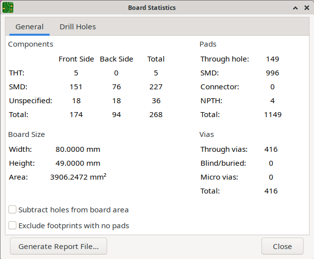
The General tab gives counts of various types of objects:
-
Footprints, separated by type (THT, SMD, or unspecified) and board side
-
Pads, separated by type (THT, SMD, connector, or NPTH)
-
Vias, separated by type (through, blind, buried, or micro)
It also displays the board dimensions, board area, and the area of front and back copper, as well as other manufacturing technology statistics such as minimum track width, minimum track clearance, and minimum drill diameter.
If Subtract holes from board area is checked, the reported board area will not include the area of any through holes in the board.
If Subtract holes from copper areas is checked, the reported copper areas will not include the area of any through holes in the board.
If Exclude footprints with no pads is checked, the component counts will exclude footprints that do not contain any pads.
The Drill Holes tab lists every unique type of drill hole on the board. Each type of hole is listed with its characteristics (shape, X and Y size, plating, pad or via type, and start and stop layers) and the count of that type of hole.
You can save the board statistics to a file by clicking the Generate Report File… button.
测量工具
测量工具允许你在 PCB 上的各点之间进行距离和角度测量。 要激活该工具,请点击右侧工具栏的 ![]() 图标,或使用快捷键 Ctrl+Shift+M。 一旦该工具被激活,点击一次以设置测量起点,然后再点击一次以完成测量。
图标,或使用快捷键 Ctrl+Shift+M。 一旦该工具被激活,点击一次以设置测量起点,然后再点击一次以完成测量。
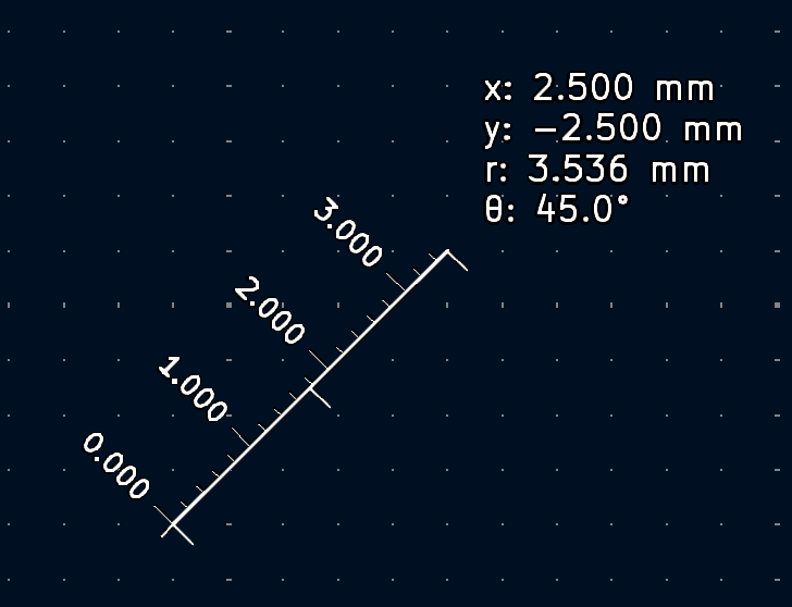
The tool displays the total (radial) distance between the points, the distance in X and Y directions, and the measured angle from horizontal. In other words, both the Cartesian and radial (polar) distances are displayed.
| 测量工具用于不需要永久显示的快速测量。 您所做的任何测量都将仅在该工具处于活动状态时显示。 要创建将显示在打印输出和打印中的永久性尺寸标注,请使用尺寸标注工具。 |
查找工具
查找工具在 PCB 中搜索文本,包括位号、封装字段和图形文本。当该工具找到一个匹配的文本时,画布会被放大,并将其置于匹配文本的中心位置,同时文本被高亮显示。使用顶部工具栏中的(![]() )按钮启动该工具。
)按钮启动该工具。
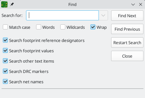
查找工具有几个选项:
Match case: Selects whether the search is case-sensitive.
Whole words only: When selected, the search will only match the search term with complete words in the PCB. When unselected, the search will match if the search term is part of a larger word in the PCB.
Wildcards: When selected, wildcards can be used in the search terms. ?
matches any single character, and * matches any number of characters. Note
that when this option is selected, partial matches are not returned: searching
for abc* will match the string abcd, but searching for abc will not.
Wrap: When selected, search results will return to the first hit after reaching the last hit.
Search footprint reference designators: Selects whether the search should apply to footprint reference designators.
Search footprint values: Selects whether the search should apply to footprint value fields.
Include hidden fields: Selects whether the search should apply to hidden footprint fields.
Search other text items: Selects whether the search should apply to other text items, including graphical text and footprint fields other than value and reference.
Search DRC markers: Selects whether the search should apply to the violation descriptions of DRC markers shown on the board.
Search net names: Selects whether the search should apply to the names of nets in the board.
搜索面板
The search panel is a docked panel that lists information about footprints, zones (copper zones and rule areas), nets, ratsnest lines (unrouted segments), text items, groups, and drills from the PCB. Show or hide the search panel with View → Panels → Search or use the Ctrl+G shortcut.
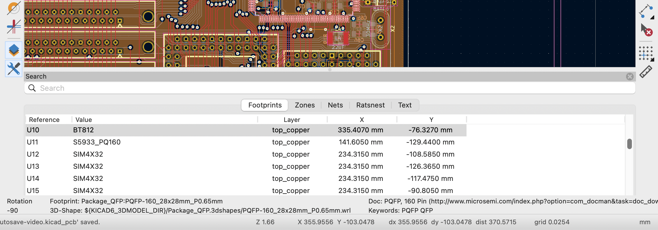
You can optionally filter the list based on a search string. When no filter is used, all items in the design are listed in the corresponding tab. Items are filtered based on their properties:
-
Footprints are filtered by the contents of their fields. You can select whether to search hidden fields by enabling the Search Hidden Fields option in the
menu. Footprints are also filtered by their metadata (library link, description, and keywords) if Search Metadata is enabled in the menu. -
Zones are filtered by the zone/rule area name.
-
Net and ratsnest items are filtered by the net name.
-
Text (text, textboxes, and dimensions) is filtered by the text content.
-
Groups are filtered by the group name.
-
Drills can be filtered by any column.
You can sort the filtered results in ascending or descending order of the value in a particular column by clicking on that column header.
Filters support wildcards: * matches any characters, and ? matches any single character. You can also use regular expressions, such as /footprint value/.
The displayed information depends on the item type:
-
All items list their name and/or value, layer, and X/Y location as applicable.
-
Footprints additionally list their library link (library name and footprint name) and description.
-
Zones additionally list their area. For copper zones, this is the filled (copper) area. For rule areas, this is the area within the outline.
-
Text additionally lists the type of text object (text, textbox, or dimension).
-
Net and ratsnest items additionally list their net name and net class.
-
Drills, where each item represents a unique type of drilled hole, list the count of each drill type, the shape of the hole, the X and Y size of the hole, the type of plating, whether it is a via or pad, and the start and stop layers.
When you click an item in the search panel, the item is selected in the editing canvas. Depending on what is configured in the ![]() menu, the board editor will also pan and/or zoom to the selected item in the editing canvas. Double-clicking an item in the search panel opens its properties dialog (for net and ratsnest items, the net classes dialog is opened instead).
menu, the board editor will also pan and/or zoom to the selected item in the editing canvas. Double-clicking an item in the search panel opens its properties dialog (for net and ratsnest items, the net classes dialog is opened instead).
3D 查看器
The 3D Viewer shows a 3-dimensional view of the board and the components on the board. You can view the board from different perspectives, show or hide different types of components, cross-probe from the PCB Editor to the 3D viewer, and generate raytraced renders of the board. Show the 3D Viewer with View → 3D Viewer or use the Alt+3 shortcut.
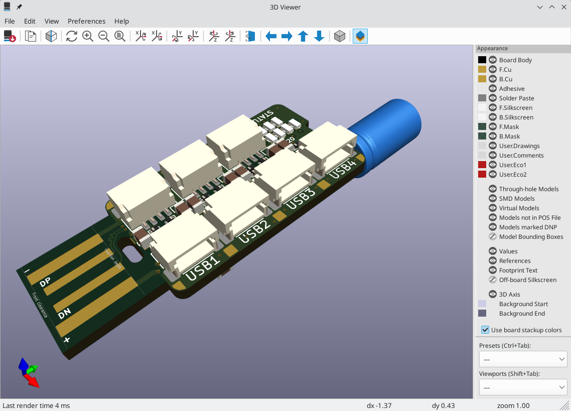
| 仅当 3D 模型文件存在并且已被 分配到封装 时,元件的 3D 模型才会出现。 |
| KiCad 标准库中的许多封装还没有为它们创建模型文件。然而,这些封装可能包含一个指向尚不存在的 3D 模型的路径,以期待将来创建 3D 模型。 |
浏览 3D 视图
用鼠标左键拖动将旋转 3D 视图。 默认情况下,这是电路板的中心,但可以通过将光标移动到所需点上并按 Space 将轴心点重置为电路板上的新点。 滚动鼠标滚轮将放大或缩小视图。 按住 Ctrl 滚动可左右平移视图,按住 Shift 滚动可上下平移视图。 使用鼠标中键拖动也可以平移视图。
The 3D Navigator is an interactive widget displayed in the 3D Viewer that provides quick access to standard orthogonal views. It consists of six spheres representing the six standard viewing directions: Front, Back, Left, Right, Top, and Bottom. Clicking any sphere will instantly reorient the camera to that viewpoint. The 3D Navigator can be shown or hidden using Preferences → Show 3D Navigator.
Different sized 3D grids can be set using the View → 3D Grid menu. Bounding boxes for each component can be enabled with Preferences → Show Model Bounding Boxes.
当 PCB 编辑器和 3D 查看器同时打开时,在 PCB 编辑器中选择一个封装也会在 3D 查看器中高亮显示该元件。高亮显示的颜色可以在 偏好设置 → 偏好设置… → 3D 查看器 → 实时渲染器 → 选择颜色 中调整。
Appearance Manager
The Appearance Manager is a panel at the right of the viewer which provides controls to manage the visibility, color, and opacity of different types of objects and board layers in the 3D view.
Each layer or type of object in the list can be individually shown or hidden by clicking its corresponding visibility icon. PCB layers can have their colors customized; double-click on the color swatch next to the item type to edit the item’s color and opacity. To use the colors selected in the Board Setup dialog’s Physical Stackup editor, enable the use board stackup colors option. If you enable the use PCB editor copper colors option, copper layers in the 3D viewer will use the colors configured in the PCB editor canvas.
You can save an appearance configuration as a preset, or load a configuration from a preset, using the Preset selector at the bottom. The Ctrl+Tab hotkey cycles through presets; press Tab repeatedly while holding Ctrl to cycle through multiple presets. Several built-in presets are available: "Follow PCB Editor" matches the visibility settings in the PCB editor, "Follow PCB Plot Settings" matches the visibility settings selected in the Plot dialog, and "legacy colors" matches the default 3D Viewer color settings from older versions of KiCad.
Finally, you can save a viewport for later retrieval using the Viewports selector at the bottom. You can quickly cycle between saved viewports using Shift+Tab; pressing Tab repeatedly while holding Shift will cycle through multiple viewports.
用 3D 查看器生成图像
The current 3D view can be saved to an image file with File → Export Image…. Before saving, you can choose the output image size and resolution. The current view can also be copied to the clipboard using the ![]() button, or Edit → Copy 3D Image to Clipboard.
button, or Edit → Copy 3D Image to Clipboard.
3D 查看器有一个光线跟踪渲染模式,它使用比默认渲染模式更精确的物理渲染模型来显示电路板。 光线追踪比默认渲染模式慢,但当需要最吸引人的视觉效果时,可以使用它。使用 ![]() 按钮,或者使用 偏好设置→光线追踪 来启用光线追踪模式。在光线追踪模式下,3D 网格和选择高亮不会显示。
按钮,或者使用 偏好设置→光线追踪 来启用光线追踪模式。在光线追踪模式下,3D 网格和选择高亮不会显示。
颜色和其他渲染选项,包括光线跟踪和非光线跟踪模式,都可以在 偏好设置 → 偏好设置… → 3D查看器 中调整。
3D 查看器控制
许多查看选项是通过顶部的工具栏控制的。
| You can edit the toolbars' contents in the Toolbar page of the 3D Viewer Preferences. |
|
Reload the 3D model |
|
Copy 3D image to clipboard |
|
Render current view using raytracing |
|
Redraw |
|
Zoom in |
|
Zoom out |
|
Fit drawing in display area |
|
Rotate X clockwise |
|
Rotate X counterclockwise |
|
Rotate Y clockwise |
|
Rotate Y counterclockwise |
|
Rotate Z clockwise |
|
Rotate Z counterclockwise |
|
Flip board view |
|
Pan board left |
|
Pan board right |
|
Pan board up |
|
Pan board down |
|
Enable/disable orthographic projection |
|
Show/hide the Appearance Manager |
网络检查
The Net Inspector is a docked panel that allows you to view statistics about all the nets in a board. It also lets you add, remove, and rename nets. To open the inspector, click the ![]() icon at the top of the Nets section of the Appearance panel, or select View → Panels → Net Inspector.
icon at the top of the Nets section of the Appearance panel, or select View → Panels → Net Inspector.
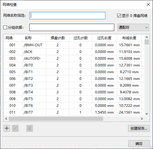
Double-clicking a net in the list will highlight that net on the board. You can also highlight a net by right clicking it and selecting Highlight Selected Net. If multiple nets are selected, this lets you highlight all of them at once. You can remove the net highlighting by right clicking the net’s row in the Net Inspector and selecting Clear Net Highlighting, in addition to the usual ways of removing net highlighting.
Clicking a column title allows you to sort the list of nets by that column. The Filter box lets you limit the listed nets to those that match the filter string. By default, the filter matches against both net names and net class names, but you can filter by just one or the other by selecting or deselecting Filter by Net Name or Filter by Netclass under the ![]() menu.
menu.
By default, nets with no connections and nets with no pads are not shown. You can choose to show them by selecting Show Unconnected Nets and Show Zero Pad Nets under the ![]() menu.
menu.
The Net Inspector shows the following statistics for each net:
-
Pad Count is the number of pads with that net, counting both surface mount and through hole pads.
-
Via Count is the number of vias with that net.
-
Via Length is the sum total length of all vias with that net. The full height of each via is always counted, even if the connections to the via are such that the full via height is not electrically used. In other words, Via Length is equal to Via Count multiplied by the stackup height of the board.
-
Track Length is the total length of all track segments in a net, not accounting for topology. For example, in a branching net structure all branches are included in the total length. The track length is also reported per copper layer.
-
Die Length is the total of all Pad to Die Length values set for pads on the net.
Each column can be shown or hidden in the ![]() → Show / Hide Columns menu. You can save the Net Inspector statistics to a CSV file by clicking
→ Show / Hide Columns menu. You can save the Net Inspector statistics to a CSV file by clicking ![]() → Save Net Inspector Report. The generated report includes all nets and columns, even if they are currently filtered or hidden in the Net Inspector.
→ Save Net Inspector Report. The generated report includes all nets and columns, even if they are currently filtered or hidden in the Net Inspector.
Grouping nets
You can group nets in the Net Inspector to organize them and view them more easily. Each group displays the total statistics for all its members, as if the group were a single net. For example, if you have a signal with a series resistor breaking the signal into two nets, you could create a group that contains both of these nets. This would allow you to analyze the total length of both nets, rather than each individually.
You can group nets by their net class by clicking ![]() → Group by netclass. Alternatively, you can create custom groups based on net name patterns. To create a new custom group, click
→ Group by netclass. Alternatively, you can create custom groups based on net name patterns. To create a new custom group, click ![]() → Add Custom Group. Any nets that contain the specified pattern in their name will be shown as part of the group and not shown outside of the group. For example, the pattern
→ Add Custom Group. Any nets that contain the specified pattern in their name will be shown as part of the group and not shown outside of the group. For example, the pattern CAN matches the nets CAN_RX and CAN_TX. Patterns are not case sensitive.
The pattern can also use regular expressions to match nets if the pattern is surrounded in slashes. For example, the pattern /^AN/ matches nets AN0, AN1, etc., but not CAN.
To remove a group and release its members back into the full list of nets, click ![]() → Remove Selected Custom Group. This action is also available in the right click menu. To remove all groups at once, click
→ Remove Selected Custom Group. This action is also available in the right click menu. To remove all groups at once, click ![]() → Remove All Custom Groups.
→ Remove All Custom Groups.
Editing nets
The Net Inspector allows you to create new nets in the board and remove or rename existing nets. To create a new net, right click in the Net Inspector and select Add Net, then provide a name for the new net. To delete a net, right click it in the list of nets and choose Delete Selected Net. If multiple nets are selected, they will all be deleted. To rename a net, right click it and choose Rename Selected Net, then provide a new name.
| Nets are usually not edited in the board. Instead, it is recommended to define nets in the schematic. Nets are typically managed in the board by creating or modifying a schematic and then using the Update PCB From Schematic tool to update the nets in the board based on the schematic design. The Net Inspector can be used to manage nets in alternate workflows that do not use a schematic. |
| Nets that are modified in the Board Editor will not effect the schematic until the schematic is updated from the PCB through the back-annotation process. |
Differences between Net Inspector and Length Tuner
The Net Inspector may report different net lengths than the length tuner, because the two tools have different purposes and calculate track/net lengths differently. In short, the Net Inspector sums up the total length of each track segment and via on a net, while the length tuner calculates the effective electrical length of a path between two points on a net. The specific differences are as follows:
-
The Net Inspector reports track length as a simple sum of the length of each track segment on a net. The length tuner calculates an effective electrical length of a net, which includes optimizing paths through pads to calculate the shortest possible path.
-
If a routed net has a branching topology, the Net Inspector total includes the length of each branch in the total. The length tuner calculates a point-to-point length; if there are any branches, the length tuner will stop at the closest branch and report the length up to the branch.
-
The Net Inspector always includes the effective via height in its via length and total length calculations. If a via connects to tracks on both the top and bottom layers, the full via height is included in the length calculation. Otherwise, only the stackup height between the connected layers is included. The length tuner calculates effective via height in the same way as the Net Inspector, but via height is only included in the length calculation when the use stackup height setting is enabled board constraint settings. If the setting is disabled, the length tuner will not include vias in its calculations at all.
Importing boards from other EDA tools
KiCad can import PCB designs from a wide range of third-party EDA tools. This allows you to migrate existing designs into KiCad without having to recreate them from scratch.
Imported boards are converted to KiCad’s native format. After import, the board can be edited, have its design rules adjusted, and be exported using any of KiCad’s output capabilities.
Importing a board creates a new KiCad board from the foreign file. It does not merge
the foreign board into an existing KiCad design. After import, save the board to create
a KiCad .kicad_pcb file.
|
Supported import formats
KiCad supports importing boards from the following EDA tools and file formats:
| Source EDA Tool | File Extension(s) | Layer Mapping | Library Import |
|---|---|---|---|
Altium Designer |
|
Yes |
Yes |
Altium Circuit Maker |
|
Yes |
No |
Altium Circuit Studio |
|
Yes |
No |
Cadence Allegro |
|
Yes |
No |
CADSTAR PCB Archive |
|
Yes |
Yes |
Eagle (Autodesk) |
|
Yes |
Yes |
EasyEDA / JLCEDA Standard |
|
No |
Yes |
EasyEDA / JLCEDA Professional |
|
No |
Yes |
Fabmaster |
|
No |
No |
gEDA / Lepton EDA |
|
No |
Yes |
P-CAD 200x |
|
No |
No |
PADS (ASCII) |
|
Yes |
No |
Solidworks PCB |
|
Yes |
No |
In addition, KiCad can import Specctra session files (.ses) to bring autorouter results back into an existing board. This is a specialized workflow described below.
How to import a board
To import a board from a supported foreign format, use File → Import → Non-KiCad Board File…. In the file dialog, change the file type dropdown to the desired import format. Select the foreign board file and click Open.
KiCad will read the foreign file and convert it to a KiCad board. Depending on the format, a layer mapping dialog may appear to let you control how the source layers are mapped to KiCad layers.
Some formats such as Eagle and Allegro share the .brd file extension. KiCad will
automatically detect the correct format based on the file contents when you select the
appropriate file type filter in the open dialog.
|
Layer mapping
Many import formats include a layer mapping step. When the importer encounters layers in the foreign file, it presents a dialog that lets you choose the corresponding KiCad layer for each source layer.
The dialog shows each source layer name alongside a dropdown where you can select the target KiCad layer. The importer provides a best-guess automatic mapping, but you should review it carefully. Key considerations:
-
Copper layers: Verify that the source copper layers map to the correct KiCad copper layers, especially for inner layers on multi-layer boards.
-
Silkscreen, solder mask, and paste layers: These should map to the corresponding front or back layer in KiCad.
-
Mechanical and documentation layers: Map these to the appropriate KiCad User layers or leave them unmapped if the content is not needed.
-
Unmapped layers: Setting a source layer to Unassigned causes that layer’s content to be skipped during import.
The formats that support layer mapping are: Altium Designer, Altium Circuit Maker, Altium Circuit Studio, Cadence Allegro, CADSTAR, Eagle, PADS, and Solidworks PCB.
Post-import cleanup
After importing a board from another EDA tool, review the result and perform any necessary cleanup. The following steps are recommended:
-
Run the Design Rule Check (DRC): Select Inspect → Design Rules Checker to identify any issues introduced during import. Foreign designs may use rules or features that do not have exact equivalents in KiCad.
-
Review board setup: Open File → Board Setup and verify the board stackup, design rules, and net classes. Import plugins translate rules on a best-effort basis, but some parameters may need manual adjustment.
-
Check footprints: Imported footprints are embedded directly in the board file. Consider replacing them with footprints from the KiCad library or your own libraries to take advantage of KiCad’s 3D models and updated pad shapes.
-
Inspect zones: Zone fills may need to be recalculated after import. Select Edit → Fill All Zones (B) to refill all copper zones.
-
Verify net assignments: Confirm that net names and net classes have been imported correctly by inspecting the Nets inspector (Inspect → Board Statistics) or by checking net properties of individual tracks and pads.
-
Save as a KiCad project: Use File → Save As… to save the imported board as a
.kicad_pcbfile within a KiCad project directory.
| Some importers produce messages in the message panel at the bottom of the editor window. Review these messages for warnings about unsupported features or items that could not be imported. |
Format-specific notes
Altium Designer
Altium Designer is one of the most widely used commercial EDA tools, and the KiCad importer provides comprehensive support for .PcbDoc files.
Supported features:
-
Board outline and cutouts
-
Copper layers (up to 32 layers), silkscreen, solder mask, paste, and mechanical layers
-
Tracks, arcs, vias (including blind and buried vias)
-
Pads (through-hole, SMD, and custom shapes)
-
Copper fills and polygon pours
-
Component placement and footprint geometry
-
Net information
-
Design rules (partial)
-
Embedded footprint libraries (cached footprints are available after import)
Known limitations:
-
Embedded OLE objects (such as images or documents) are not imported.
-
Some complex design rules may not have direct KiCad equivalents and will be simplified.
-
Differential pair rules are imported on a best-effort basis.
-
Altium-specific features like Situs autorouter data or embedded simulation configurations are not supported.
In addition to board import, KiCad can import Altium footprint libraries (.PcbLib) and integrated libraries (.IntLib) directly through the footprint library manager.
Altium Circuit Maker
Altium Circuit Maker files (.CMPcbDoc) use the same underlying format as Altium Designer with minor variations. The importer handles these files the same way as Altium Designer boards. Layer mapping is supported.
Altium Circuit Studio
Altium Circuit Studio files (.CSPcbDoc) are supported similarly to Altium Designer. The importer applies layer mapping and converts the board contents using the same parsing engine.
Cadence Allegro
KiCad can import Cadence Allegro binary .brd files directly.
Supported features:
-
Board outline
-
Copper layers and signal routing
-
Padstacks and vias
-
Component placement
-
Net information
-
Layer mapping with automatic suggestions
Known limitations:
-
Allegro design rules and constraints are not fully imported.
-
Flex-circuit layer stackup features are not supported.
-
Some Allegro-specific pad shapes may be approximated.
Allegro .brd files use a binary format that is distinct from Eagle .brd files (which
are XML). KiCad identifies the correct format automatically based on file content.
|
CADSTAR PCB Archive
CADSTAR PCB Archive files (.cpa) from Zuken’s CADSTAR tool can be imported into KiCad.
Supported features:
-
Board outline and templates
-
Full copper layer stackup
-
Tracks, vias, and copper pours
-
Component placement with footprint geometry
-
Net and net class information
-
Layer mapping
-
Footprint library import (footprints from the
.cpaarchive can be loaded through the footprint library manager)
Known limitations:
-
CADSTAR-specific template areas may be approximated or simplified.
-
Some advanced constraint features may not be converted.
Eagle (Autodesk)
KiCad has mature support for importing Eagle .brd files in XML format (Eagle version 6.x and later).
Supported features:
-
Board outline
-
All copper layers and signal layers
-
Tracks, vias, and polygons
-
SMD and through-hole pads with design rule-based annular ring sizing
-
Component placement and package (footprint) geometry
-
Net list and net class definitions
-
Design rules (converted to KiCad equivalents where possible)
-
Layer mapping with intelligent defaults
-
Embedded footprint libraries
Known limitations:
-
Eagle’s ULP scripts and CAM jobs are not imported.
-
Some Eagle-specific DRC rules (e.g., per-signal clearances) may be simplified.
-
Binary Eagle files (created before Eagle version 6.x) are not supported; these must first be opened and re-saved as XML in Eagle.
In addition to board import, KiCad can import Eagle footprint libraries (.lbr) through the footprint library manager.
When migrating from Eagle, you can also import Eagle schematic files (.sch) in the
KiCad Schematic Editor to bring over the full design.
|
EasyEDA / JLCEDA Standard
KiCad can import board files from EasyEDA (also known as JLCEDA Standard edition), the free web-based EDA tool from JLCPCB.
Accepted file types: .json and .zip
To obtain files for import, export your design from EasyEDA using its Export EasyEDA option, which produces a JSON file or a ZIP archive containing the board data.
Supported features:
-
Board outline
-
Copper layers and routing
-
Pads and vias
-
Component placement
-
Net information
-
Embedded footprint libraries
Known limitations:
-
Some custom pad shapes may not convert exactly.
-
Panelization data is not imported.
EasyEDA / JLCEDA Professional
KiCad can import project files from EasyEDA Professional (also known as JLCEDA Professional), the desktop version of JLCEDA.
Accepted file types: .epro and .zip
For multi-board projects, KiCad will present a project chooser dialog to let you select which board within the project to import.
Supported features:
-
Board outline
-
Copper layers and routing
-
Pads and vias
-
Component placement
-
Net information
-
Footprint libraries (
.elibzfiles can also be imported through the footprint library manager)
Known limitations:
-
Some advanced features specific to EasyEDA Pro may not have KiCad equivalents.
Fabmaster
KiCad can import Valor/Mentor Fabmaster files (.txt, .fab). These files contain fabrication data including board geometry, component placements, and layer information.
Known limitations:
-
Fabmaster files contain manufacturing-oriented data and may not include full design intent (e.g., schematic connectivity).
-
Layer mapping is not interactive; layers are assigned automatically.
-
Net information may be incomplete depending on what was exported from the source tool.
gEDA / Lepton EDA
KiCad can import board files from gEDA PCB and Lepton EDA, the open-source EDA suite.
Accepted file types: .pcb
Supported features:
-
Board layers and routing
-
Vias
-
Component (element) placement
-
Net list information
-
Footprint libraries (gEDA
.fpfootprint files can be imported through the footprint library manager)
Known limitations:
-
gEDA’s layer model is simpler than KiCad’s; some layer assignments may need adjustment after import.
P-CAD
KiCad can import P-CAD 200x ASCII board files (.pcb).
P-CAD was a legacy EDA tool that was acquired by Altium and eventually discontinued. If you have P-CAD designs, you can bring them into KiCad using this importer.
Known limitations:
-
Only the ASCII
.pcbformat is supported; the binary format is not. -
P-CAD design rules are not imported.
-
Some P-CAD-specific features may not have KiCad equivalents.
PADS
KiCad supports importing boards from Siemens (Mentor Graphics) PADS in both ASCII and binary formats.
PADS ASCII (.asc): This is the text-based export format from PADS Layout. To generate
this file, use the File → Export function in PADS Layout and choose the ASCII format.
Supported features:
-
Board outline
-
Board setup (layer stackup)
-
Copper layers and routing (tracks and vias)
-
Pads and footprints
-
Copper pours and zones
-
Net information
-
Text and dimensions
-
Keepout areas
-
Layer mapping with intelligent defaults
Known limitations:
-
Some PADS-specific pad shapes or padstack definitions may be approximated.
-
Design rules and constraints from PADS are converted on a best-effort basis.
-
Reuse block definitions may not be fully preserved.
Solidworks PCB
KiCad can import Solidworks PCB files (.SWPcbDoc). Solidworks PCB (formerly PCBWorks) uses a format derived from Altium, and the importer shares much of its code with the Altium Designer importer.
Layer mapping is supported. The same considerations that apply to Altium Designer imports generally apply to Solidworks PCB imports as well.
Importing Specctra session files
The Specctra DSN/SES workflow is used with external autorouters. Unlike the board importers described above, the Specctra session import does not create a new board. Instead, it applies routing results from an autorouter back onto an existing KiCad board.
The typical workflow is:
-
Export the board to Specctra DSN format: select File → Export → Specctra DSN….
-
Run the external autorouter on the
.dsnfile to produce a session file (.ses). -
Import the session file back into KiCad: select File → Import → Specctra Session….
KiCad will read the .ses file and add the routed tracks and vias to the board. The board’s footprints, nets, and board outline must match the original export for the import to succeed.
| The Specctra session import only adds routing; it does not modify footprints, net lists, or the board outline. |
生成输出
KiCad can generate and export files in a number of different formats useful for manufacturing PCBs and interfacing with external software. This functionality is available in the File menu in a few different sections.
-
The Fabrication Outputs section contains the most common operations needed to prepare a PCB for fabrication.
-
The Export section contains tools for generating files that can be read by external software.
-
The Plot function allows you to export 2D line drawings of the PCB in various formats.
-
The Print function allows you to send a view of the PCB to a 2D printer.
Plotting (Gerber / PostScript / SVG / DXF / PDF / PNG)
KiCad uses Gerber files as its primary plotting format for PCB manufacturing. To create Gerber files, select File → Fabrication Outputs → Gerbers (.gbr)…. The Plot dialog will open, allowing you to configure and generate Gerber files.
In addition to Gerber files, the Plot dialog is also used to create PostScript, SVG, DXF, PDF, and PNG outputs. You can also open the Plot dialog with File → Plot…, or by clicking the ![]() button in the top toolbar. You can select the output format with the Plot format dropdown.
button in the top toolbar. You can select the output format with the Plot format dropdown.
Most plotting options are common to all of the plotted output formats, but there are also some options that are specific to each format.
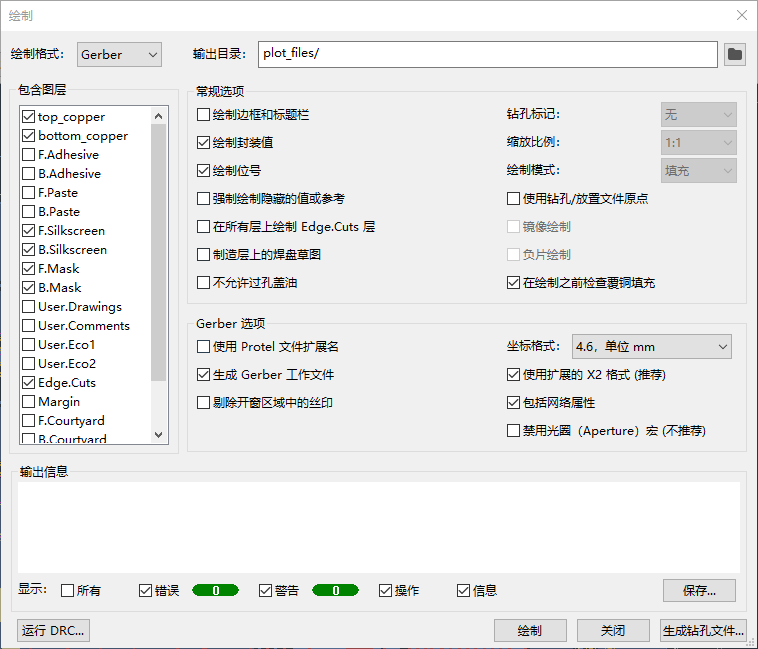
The Plot button generates output files according to the selected options. Messages from the plotting process are shown in the Output Messages panel, and can be filtered by the checkboxes.
The Generate Drill Files… button opens the Generate Drill Files dialog. Run DRC… opens the Design Rules Checker.
绘图选项
-
Include Layers: Check that every layer used on your board is enabled in the list. Disabled layers will not be plotted.
-
Plot on All Layers: Selected layers will be included in the plot for each layer selected in the include layers list. The additional layers are plotted on top of the base layer. You can reorder these layers using the arrow buttons at the bottom; items that are lower in the list are plotted after (on top of) items that are higher in the list.
-
Design variant: Specify the design variant to plot.
-
Output directory: Specify the location to save plotted files. If this is a relative path, it is created relative to the project directory. Use the
 button
to open the output directory in a file browser.
button
to open the output directory in a file browser. -
Plot drawing sheet: If enabled, the drawing sheet border and title block will be plotted on each layer. This should usually be disabled when plotting Gerber files.
-
Subtract soldermask from silkscreen: When enabled, silkscreen will be automatically removed from board areas that aren’t covered by soldermask.
-
Indicate DNP on fabrication layers: If enabled, fabrication layers (
F.FabandB.Fab) will indicate when a footprint has the DNP (Do Not Populate) attribute set. DNP footprints are either not plotted on the fabrication layers (Hide) or are plotted with an X drawn through them on the front and back fabrication layer (Cross-out). -
Sketch pads on fabrication layers: If enabled, the outlines of footprint pads will be drawn on fabrication layers (
F.FaborB.Fab). If Include pad numbers is enabled, pad numbers will be drawn as well. -
Drill marks: For plot formats other than Gerber, marks may be plotted at the location of all drilled holes. Drill marks may be created at the actual size (diameter) of the finished hole, or at a smaller size.
-
Scaling: For plot formats that support scaling other than 1:1, the plot scale may be set. The Auto scaling setting will scale the plot to fit the specified page size.
-
Use drill/place file origin: When enabled, the coordinate origin for plotted files will be the drill/place file origin set in the board editor. When disabled, the coordinate origin will be the absolute origin (top left corner of the worksheet).
-
Mirrored plot: For some plot formats, the output may be mirrored horizontally when this option is set.
-
Negative plot: For some plot formats, the output may be set to negative mode. In this mode, shapes will be drawn for the empty space inside the board outline, and empty space will be left where objects are present in the PCB.
-
Check zone fills before plotting: When enabled, zone fills will be checked (and refilled if outdated) before generating outputs. Plot outputs may be incorrect if this option is disabled!
| Versions of KiCad before 9.0 had a global control for tenting vias while plotting. Since KiCad 9.0, via tenting is globally controlled in Board Setup, and can be overridden in the properties dialog for each via. |
Gerber 选项
-
Use Protel filename extensions: When enabled, the plotted Gerber files will be named with file extensions based on Protel (
.GBL,.GTL, etc). When disabled, the files will have the.gbrextension. -
Generate Gerber job file: When enabled, a Gerber job file (
.gbrjob) will be generated along with any Gerber files. The Gerber job file is an extension to the Gerber format that includes information about the PCB stackup, materials, and finish. More information about Gerber job files is available at the Ucamco website. -
Coordinate format: Configure how coordinates will be stored in the plotted Gerber files. Check with your manufacturer for their recommended setting for this option.
-
Use extended X2 format: When enabled, the plotted Gerber files will use the X2 format, which includes information about the netlist and other extended attributes. This format may not be compatible with older CAM software used by some manufacturers.
-
Include netlist attributes: When enabled, the plotted Gerber files will include netlist information that can be used for checking the design in CAM software. When X2 format mode is disabled, this information is included as comments in the Gerber files.
-
Disable aperture macros: When enabled, all shapes will be plotted as primitives rather than by using aperture macros. This setting should only be used for compatibility with old or buggy CAM software when requested by your manufacturer.
Postscript 选项
-
Scale factor: Controls how coordinates in the board file will be scaled to coordinates in the PostScript file. Using a different value for X and Y scale factors will result in a stretched / distorted output. These factors may be used to correct for scaling in the PostScript output device to achieve an exact-scale output.
-
Track width correction: A global factor that is added (or subtracted, if negative) from the size of tracks, vias, and pads when plotting a PostScript file. This factor may be used to correct for errors in the PostScript output device to achieve an exact-scale output.
-
Force A4 output: When enabled, the generated PostScript file will be A4 size even if the KiCad board file is a different size.
SVG 选项
-
Precision: Controls how many significant digits will be used to store coordinates.
-
Output mode: Controls whether the generated SVG file is in color or black and white.
-
Fit page to board: When enabled, the generated SVG will have the same size as the board outline.
DXF 选项
-
Plot graphic items using their contours: Graphic shapes in DXF files have no width. This option controls how graphic shapes with a width (thickness) in a KiCad board are plotted to a DXF file. When this option is enabled, the outer contour of the shape will be plotted. When this option is disabled, the centerline of the shape will be plotted (and the shape’s thickness will not be visible in the resulting DXF file).
-
Use KiCad font to plot text: When enabled, text in the KiCad design will be plotted as graphic shapes using the KiCad font. When disabled, text will be plotted as DXF text objects, which will use a different font and will not appear in exactly the same position and size as shown in the KiCad board editor.
-
Single document: When enabled, all selected layers will be plotted in a single DXF file, with each PCB layer plotted as a separate DXF layer.
-
Export units: Controls the units that will be used in the DXF file. Since the DXF format has no specified units system, you must export using the same units setting that you want to use for importing into other software.
PDF options
-
Output mode: Controls whether the generated PDF file is in color or black and white.
-
Generate property popups for front footprints: When enabled, interactive popups will be added to the generated PDF containing part information for each footprint on the front of the board.
-
Generate property popups for back footprints: When enabled, interactive popups will be added to the generated PDF containing part information for each footprint on the back of the board. For details, see the Schematic Editor documentation.
-
Generate metadata from AUTHOR and SUBJECT variables: Sets the Author and Subject PDF document properties for the generated PDF based on the
AUTHORandSUBJECTproject text variables, if you have defined them. -
Single document: When enabled, each layers will be plotted as an individual sheet within a single PDF document. When disabled, each layer will be plotted as a separate PDF file.
-
Background color: Sets the background color for the PDF plot. Background color is not available when the output mode is black and white.
PNG options
-
DPI: Sets the pixel density of the output file.
-
Anti-alias: Controls whether the output file should be anti-aliased.
钻孔文件
KiCad can generate CNC drilling files required by most PCB manufacturing processes in either Excellon or Gerber X2 format. KiCad can also generate a drill map: a graphical plot of the board showing drill locations. To open the dialog, select the File → Fabrication Outputs → Drill Files (.drl)…, or click the Generate Drill Files… button in the Plot dialog.
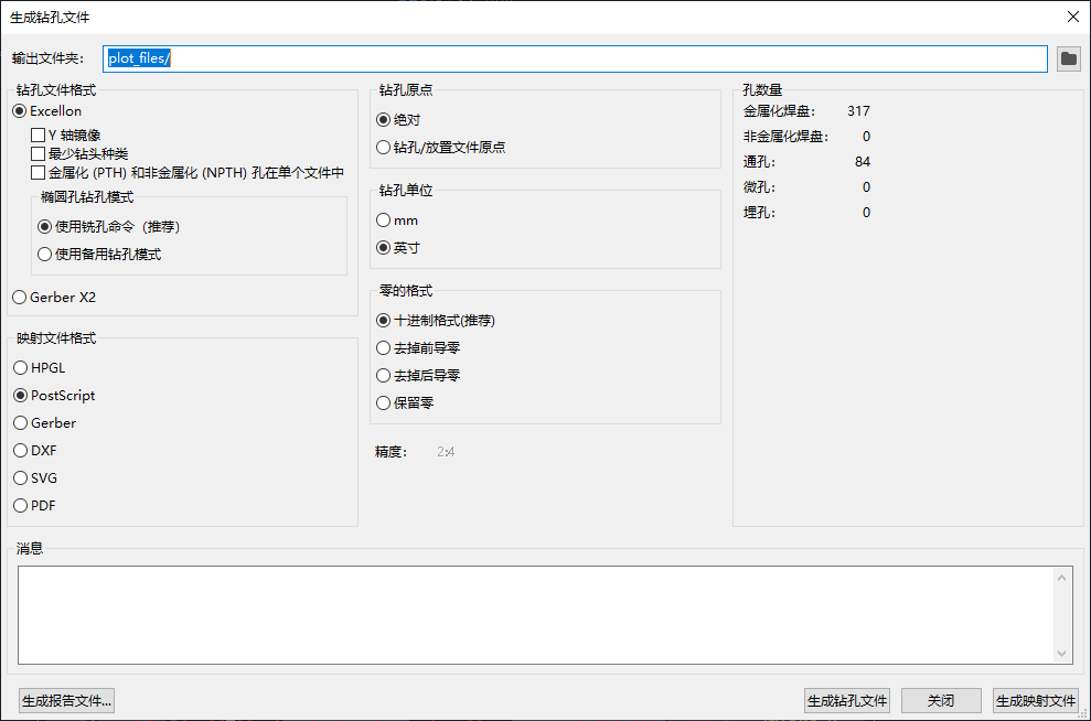
There are several options for generating drill files.
-
Output folder: Choose the folder to save generated drill and map files to. If a relative path is entered, it will be relative to the project directory.
-
Drill file format: Choose whether to generate Excellon drill files (required by most PCB manufacturers) or Gerber X2 files.
-
Mirror Y axis: For Excellon files, choose whether or not to mirror the Y-axis coordinate. This option should in general not be used when having PCBs manufactured by a third party, and is provided for convenience for users who are making PCBs themselves.
-
Minimal header: For Excellon files, choose whether to output a minimal header rather than a full file header. This option should not be enabled unless requested by your manufacturer.
-
PTH and NPTH in single file: By default, plated holes and non-plated holes will be generated in two different Excellon files. With this option enabled, both will be merged into a single file. This option should not be enabled unless requested by your manufacturer.
-
Use alternate drill mode for oval holes: Controls how oval holes are represented in an Excellon drill file. When not enabled, a route command is used to represent oval holes. This is correct for most manufacturers. Only choose the Use alternate drill mode setting if requested by your manufacturer.
-
Generate map: Choose whether to generate a drill map and, if so, in which format. Supported formats are Postscript, Gerber X2, DXF, SVG, and PDF.
-
Origin: Choose the coordinate origin for drill files. Absolute will use the page origin at the top left corner. Drill/place file origin will use the origin specified in the board design.
-
Drill units: Choose the units for drill coordinates and sizes.
-
Zeros: Controls how zeroes are formatted in an Excellon drill file. Select an option here based on your manufacturer’s recommendations.
IPC-2581
IPC-2581 files are XML files that contain complete fabrication and assembly data for a board design. If your manufacturer accepts IPC-2581 files, these can replace Gerber files, drill files, and component placement files. To create an IPC-2581 file, select File → Fabrication Outputs → IPC-2581 File (.xml)….
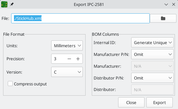
There are several options for generating IPC-2581 output.
-
File: Choose the filename for the generated IPC-2581 file. If a relative path is entered, it will be relative to the project directory.
-
Units: Choose the units for the generated file. Can be millimeters or inches.
-
Precision: Choose the number of digits after the decimal point for numbers in the generated file.
-
Version: Choose the IPC-2581 standard version (B or C).
-
Compress output: If enabled, the generated file will be compressed as a ZIP file.
-
Internal ID: Choose the footprint field to use for the BOM’s internal ID column. This can be a generated unique ID or set to any footprint field in the design.
-
Manufacturer P/N: Choose the footprint field to use for the BOM’s manufacturer part number column. This can be omitted or set to any footprint field in the design.
-
Manufacturer: Choose the footprint field to use for the BOM’s manufacturer column. This can be omitted or set to any footprint field in the design.
-
Distributor P/N: Choose the footprint field to use for the BOM’s distributor part number column. This can be omitted or set to any footprint field in the design.
-
Distributor: Choose the footprint field to use for the BOM’s distributor column. This can be omitted or set to any footprint field in the design.
-
BOM revision: Specify the value for the BOM’s revision field. If omitted, the value from the schematic root sheet’s
Revisionfield is used.
ODB++
ODB++ output is a database of files that contains complete fabrication and assembly data for a board design. If your manufacturer accepts ODB++ files, these can replace Gerber files, drill files, and component placement files. To create an ODB++ file, select File → Fabrication Outputs → ODB++ Output File….
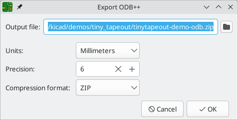
There are several options for generating ODB++ output.
-
Output file: Choose the filename for the generated ODB++ file. If a relative path is entered, it will be relative to the project directory.
-
Units: Choose the units for the generated file. Can be millimeters or inches.
-
Precision: Choose the number of digits after the decimal point for numbers in the generated file.
-
Compression format: Choose the type of compression for the generated output. Can be ZIP, TGZ, or none. If none, the output will be a folder.
Component placement (position) files
Component placement files, or position files, are text files that list each component (footprint) on the board along with its center position and orientation. These files are usually used for programming pick-and-place machines, and may be required by your manufacturer if you are ordering fully-assembled PCBs. To create placement files, select File → Fabrication Outputs → Component Placement (.pos, .gbr)….
| A footprint will not appear in generated placement files if the "Exclude from position files" option is enabled for that footprint. This may be used for excluding certain footprints that do not represent physical components to be assembled. You can also optionally exclude DNP or "Exclude from BOM" components, depending on your manufacturer’s requirements. |
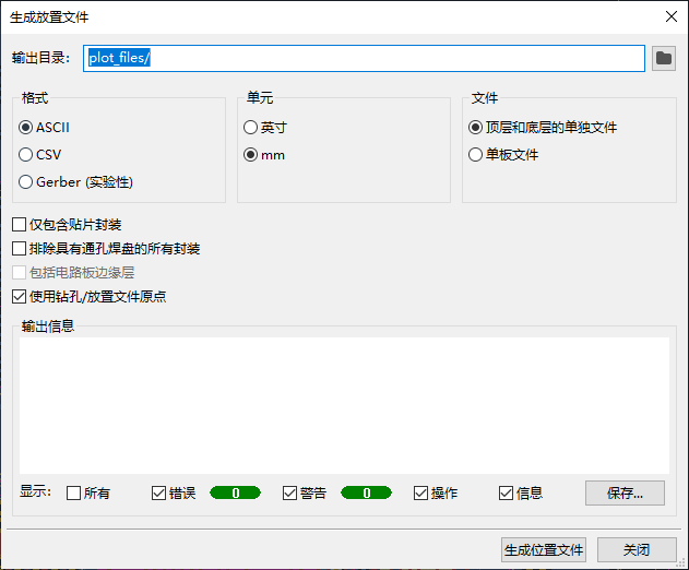
There are several options for generating placement files.
-
Design variant: Select the design variant to use for generating the placement file.
-
Output directory: Select the location to save the output placement file(s).
-
Format: Choose between generating a plain text (UTF-8), comma-separated text (CSV), or Gerber X3 placement file format.
-
Units: Choose the units for component locations in the placement file.
-
Include only SMD footprints: When enabled, only footprints with the SMD fabrication attribute will be included. Check with your manufacturer to determine if non-SMD footprints should be included or excluded from the position file.
-
Exclude all footprints with through hole pads: When enabled, footprints will be excluded from the placement file if they contain any through-hole pads, even if their fabrication type is set to SMD.
-
Exclude all footprints with the Do Not Populate flag set: When enabled, footprints will be excluded from the placement file if they have the Do Not Populate attribute set. Check with your manufacturer to determine if DNP components should be included or excluded from the position file.
-
Exclude all footprints with the Exclude from BOM flag set: When enabled, footprints will be excluded from the placement file if they have the Exclude from BOM attribute set.
-
Include board edge layer: For Gerber placement files, controls whether or not the board outline is included with the footprint placement data.
-
Use drill/place file origin: When enabled, component positions will be relative to the drill/place file origin set in the board design. When disabled, the positions will be relative to the page origin (upper left corner).
-
Use negative X coordinates for footprints on bottom layer: When enabled, the X coordinates will be flipped (negated) for footprints on the bottom layer.
-
Generate single file with both front and back positions: When enabled, positions for front and back footprints will be saved in a single file. When disabled, separate files will be generated for front and back footprints.
Footprint reports
This exporter generates a text report of all the footprints in the board. To create a footprint report, select File → Fabrication Outputs → Footprint Report (.rpt)…. There are no configurable options.
IPC-D-356 netlists
This exporter generates a netlist of the board in IPC-D-356 format, which is suitable for manufacturing checks of bare PCBs. To create an IPC-D-356 netlist, select File → Fabrication Outputs → IPC-D-356 Netlist File….
The save dialog has one configurable option: if Do not export unconnected pads is checked, pads with no net connection will not be included in the export.
Bill of Materials
This exporter generates a Bill of Materials (BOM) in CSV format containing all of the footprints on the board. To create a Bill of Materials, select File → Fabrication Outputs → Bill of Materials…. There are no configurable options.
| This BOM exporter is included for legacy reasons, and is not recommended. Instead, it is recommended to use the BOM Exporter in the Schematic Editor, which supports multiple output formats and is highly configurable. |
打印
KiCad can print the board view to a standard printer using the print function. To print a board, select File → Print….
| While the Print action can be used with a PDF printer to generate a PDF, the Plot function is recommended instead as it is more configurable and may be more accurate. |
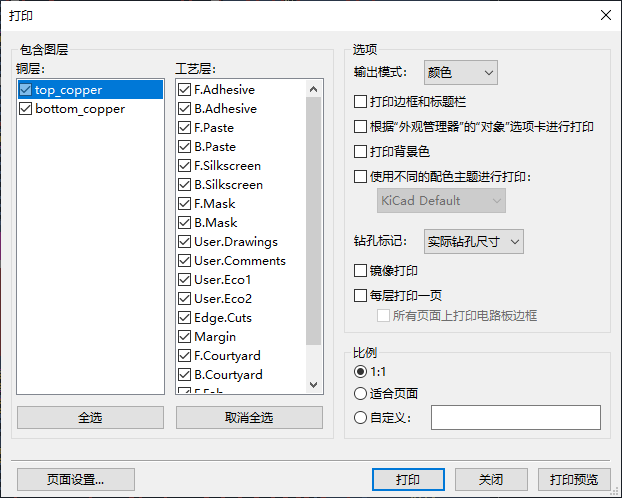
There are several options for printing.
-
Include layers: Select the layers to include in the printout. Unselected layers will be invisible. Right-click the list for layer selection commands.
-
Output mode: Choose whether to print in black and white or full color.
-
Print drawing sheet: When enabled, the page border and title block will be printed.
-
Print according to objects tab of appearance manager: When enabled, any objects that have been hidden in the Objects tab of the Appearance panel will be hidden in the printout. When disabled, these objects will be printed if the layer they appear on is selected in the Included Layers area.
-
Print background color: When printing in full color, this option controls whether or not the view background color will be printed.
-
Use a different color theme for printing: When printing in full color, this option allows a different color theme to be used for printing. When disabled, the color theme used by the board editor will be used for printing.
-
Drill marks: Controls whether to show drilled holes at their actual size, at a small size, or hide them from the printout.
-
Print mirrored: When enabled, the printout will be mirrored horizontally.
-
Print one page per layer: When enabled, each layer selected in the Included Layers area will be printed to an individual page. If this option is enabled, the Print board edges on all pages option controls whether to add the Edge.Cuts layer to each printed page.
-
Scale: controls the scale of the printout relative to the page size configured in Page Setup.
Specctra DSN
The Specctra DSN exporter creates a file suitable for importing into certain third-party autorouter software. To create a Specctra DSN file, select File → Export → Specctra DSN…. There are no configurable options.
GenCAD
The GenCAD exporter creates a GenCAD file for fabrication, testing, or importing into other software. To create a GenCAD file, select File → Export → GenCAD….
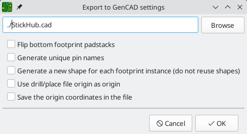
There are several options for generating GenCAD files.
-
Flip bottom footprint padstacks: If enabled, separate flipped padstack definitions will be added for bottom-side footprints. This may be necessary for importing into some third-party software.
-
Generate unique pin names: If enabled, a suffix will be added to each pin name so that no footprint in the generated file will have two pins with the same name.
-
Generate a new shape for each footprint instance: If enabled, a unique footprint will be output for every footprint instance, even if two footprints are identical.
-
Use drill/place file origin as origin: If enabled, coordinates in the generated file will be relative to the drill/place file origin.
-
Save the origin coordinates in the file: If enabled, the selected origin coordinates will be included in the generated file. If not enabled, the origin in the generated file will be set to (0,0).
VRML
The VRML exporter creates a VRML (.wrl) 3D model file containing the PCB and any VRML files specified in footprints. VRML models are suitable for use in applications where visual appearance is important and dimensional accuracy is not critical. To create a VRML file, select File → Export → VRML….
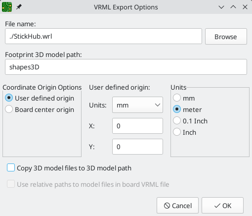
There are several options for generating VRML files.
-
User defined origin: Selects the origin for the generated model. If enabled, you can manually specify the origin point relative to the configured display origin. If not enabled, the origin point is at the configured display origin.
-
Units: Selects the unit system for the generated model. Dimensions in the generated model will be scaled appropriately.
-
Ignore 'Do not populate' components: If enabled, VRML files for footprints with the 'Do not populate' attribute set will not be included.
-
Ignore 'Unspecified' components: If enabled, VRML files for footprints with the 'Unspecified' footprint type will not be included.
-
Copy 3D model files to 3D model path: If enabled, VRML files referenced in footprints will be copied into a subdirectory of the directory containing the generated board VRML model, and the generated model will reference the copied files. The subdirectory name is set by the footprint 3D model path field. If disabled, VRML files referenced in footprints will be embedded in the generated VRML files.
-
Use relative paths to model files in board VRML file: If enabled, references to external models will use paths relative to the generated board VRML file. If disabled, the references will use absolute paths. This option is only available when the copy 3D model files to 3D model path option is enabled.
IDF
IDF 导出器导出一个 IDFv3 兼容的板(.emn)和库(.emp)文件,用于向机械 CAD 软件传递机械尺寸。导出器导出板子的边框和切口,所有的焊盘和安装孔,包括开槽孔,以及元件的边框;这是与机械设计师互动所需的最基本的机械数据集。IDFv3 规范中描述的所有其他实体目前都没有导出。
| You must attach IDF component models to your design’s footprints before they will be included in the exported model. For more information on attaching models to footprints, see the footprint documentation. Some IDF-specific guidance is included in the Advanced Topics documentation. |
| For more information on creating IDF component models, including descriptions of the IDF utility tools included with KiCad, see the Advanced Topics documentation. |
一旦为所有需要的元件指定了模型,就可以导出电路板的模型。在 PCB 编辑器中,选择文件 → 导出 → IDFv3…。
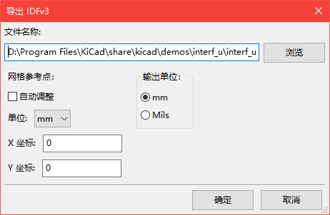
There are several options for generating IDF files.
-
Set board reference point: Choose where the exported model’s reference point is relative to the display origin. If this option is not selected, KiCad will set the reference point to the centroid of the PCB.
-
Output units: Choose whether the exported model’s units are millimeters or mils.
-
Ignore 'Do not populate' components: If enabled, IDF files for footprints with the 'Do not populate' attribute set will not be included.
-
Ignore 'Unspecified' components: If enabled, IDF files for footprints with the 'Unspecified' footprint type will not be included.
输出结果可以直接在机械 CAD 应用程序中查看,或使用 idf2vrml 工具 转换为 VRML。
3D models (STEP / GLB / BREP / XAO / PLY / STL / STPZ / U3D / PDF)
The 3D model exporter creates a 3D model file from the PCB and any STEP files specified in footprints. A number of formats are supported:
-
STEP
-
GLB (binary glTF)
-
BREP (OCCT-native boundary representation)
-
XAO (SALOME/Gmsh)
-
PLY
-
STL
-
STPZ (GZIP-compressed STEP)
-
U3D
-
PDF
Different formats may be appropriate for different usecases. For example, STEP models are suitable for use in mechanical CAD applications, while XAO models are useful for physical simulations.
KiCad’s footprint library includes both STEP and VRML (.wrl) versions of each model.
However, footprints in KiCad’s library only reference the VRML versions of the models.
VRML models are not included in STEP exports, but the STEP exporter will instead include
the corresponding STEP version of the model if the subsitute similarly named models
option is enabled.
|
To use the 3D model exporter, select File → Export → STEP / GLB / BREP / XAO / PLY / STL….
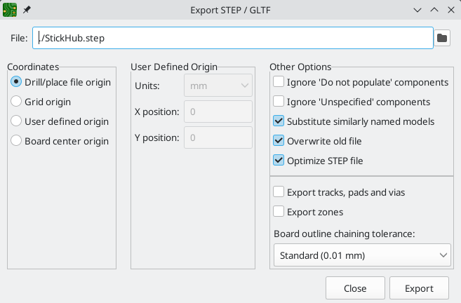
Choose a 3D model format from the Format dropdown menu and specify an output filename in the File selector. The Variant dropdown selects the design variant to use for the export.
There are a number of options for configuring the output model.
Board options
-
Export board body: If enabled, the board body (non-copper) will be modeled in the exported model.
-
Cut vias in board body: If enabled, via holes will be cut in the board body even if conductor layers are not modeled.
-
Export silkscreen: If enabled, silkscreen will be modeled in the exported model. Silkscreen is modeled as a set of flat faces; it is not three-dimensional.
-
Export solder mask: If enabled, solder mask will be modeled in the exported model. Solder mask is modeled as a set of flat faces; it is not three-dimensional.
-
Export components: If enabled, 3D models for components will be included in the exported model (but see Substitute similarly named models, below). If All components is selected, models for all components in the PCB will be included. If Only selected is chosen, only models for the footprints currently selected in the board will be included. If Components matching filter is selected, only models for footprints with references matching the filter will be included. The filter supports wildcards and commas, so
C1,R*will includeC1and all resistors.
Conductor options
-
Export tracks and vias: If enabled, tracks and vias on outer layers will be modeled in the exported model.
-
Export pads: If enabled, pads will be modeled in the exported model.
0.005mm of additional metal thickness is added by the exporter to each pad.
This causes pads to be separate faces in the exported model, distinct from the surrounding metal.
If this additional thickness is not wanted, you can use kicad-cli with the --no-extra-pad-thickness option to export a 3D model without the additional pad thickness.
|
-
Export zones: If enabled, zones on outer layers will be modeled in the exported model.
-
Export inner conductor layers: If enabled, inner conductor layers will be modeled in the exported model.
-
Fuse shapes (time consuming): If enabled, intersecting geometry will be fused into a single shape. This may make the exported file easier to work with in some tools, but it also significantly increases the export time.
-
Fill all vias: If enabled, via holes will not be cut in conductor layers.
-
Net filter (supports wildcards): If filled, only conductors corresponding to nets that match the filter will be modeled. The filter supports wildcards, so
/tx_*will model/tx_pand/tx_nconductors.
Coordinates
-
Coordinates: Selects the origin for the generated model. If user defined origin is selected, you can manually specify the origin point relative to the configured display origin.
Other options
-
Ignore 'Do not populate' components: If enabled, components with the DNP attribute set will not be included in the exported model.
-
Ignore 'Unspecified' components: If enabled, components with the Unspecified footprint type will not be included in the exported model.
-
Substitute similarly named models: VRML models cannot be used in STEP, BREP, or XAO exports, but if this option is enabled the exporter will look for an identically named STEP model to include in the export instead of a footprint’s specified VRML model. Note that footprints in KiCad’s footprint library specify VRML models, but suitably named STEP models are also included for each VRML model. Therefore this option must be enabled in order to export 3D models for footprints from KiCad’s library using this dialog.
-
Overwrite old file: If enabled, the exported model will overwrite an existing file with the same name.
-
Don’t write P-curves to STEP file If enabled, parametric curves will be disabled in the exported STEP/STPZ model. This reduces the file size, but may reduce compatibility with some software.
-
Board outline chaining tolerance: Controls the minimum distance between two points for the points to be considered coincident. If the board outline in the exported model is not contiguous, try increasing this tolerance.
Footprint association (CMP) files
CMP files are used to sync footprint assignments and some other footprint fields between the PCB and the schematic. You can export CMP files by selecting File → Export → Footprint Association (.cmp) File… and import CMP files into the schematic using the Schematic Editor’s File → Import → Footprint Assignments menu item. This provides a very limited form of backannotation. It is recommended to use the Update Schematic from PCB tool instead. There are no configurable options.
Hyperlynx
The Hyperlynx exporter creates a file suitable for importing into Mentor Graphics (Siemens) HyperLynx simulation and analysis software. To create a HyperLynx file, select File → Export → Hyperlynx…. There are no configurable options.
Design variants
Design variants allow a single PCB to represent multiple product configurations. Variants are defined in the Schematic Editor and transferred to the board through Update PCB from Schematic. The PCB Editor provides tools for viewing variant effects, selecting the active variant, and generating variant-specific manufacturing output.
For information on creating variants and editing variant data, see Design variants in the Schematic Editor manual.
Selecting a variant in the PCB editor
The main toolbar contains a variant selector dropdown, identical in behavior to the one in the Schematic Editor. Selecting a variant updates the board view to reflect that variant’s component states.
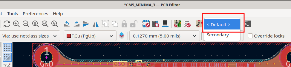
When a variant is active:
-
Components marked DNP in that variant display an X on the fabrication layers.
-
Field text (Value, Footprint, custom fields) reflects the variant’s overrides.
-
Text items using
${VARIANT}or${VARIANT_DESC}resolve to the active variant’s name and description.
Selecting <Default> returns to the base design with no overrides applied.
Viewing variant effects
Component visibility and DNP
When a variant is active, components marked DNP for that variant are displayed with an X drawn across them on the fabrication layers (F.Fab and B.Fab). This matches the behavior of the base design’s DNP attribute, but is controlled per-variant.
The board view updates in real time as you switch between variants, so you can quickly compare which components are fitted in each configuration.
3D 查看器
The 3D viewer respects the active variant. Components marked DNP in the current variant are hidden from the 3D view, giving you an accurate visual representation of how the assembled board will look for each product configuration.
To see a specific variant in the 3D viewer, select it from the toolbar dropdown in the PCB Editor before opening (or while viewing) the 3D model.
Footprint properties
When a non-default variant is active, both the Properties panel and the Footprint Properties dialog (double-click a footprint) show the variant’s overrides instead of the base design values. This includes field values, the DNP attribute, and the exclusion flags. Edit variant overrides for individual footprints through either the panel or the dialog.
Generating variant-aware outputs
Several output dialogs in the PCB Editor include a variant selector. Choosing a variant before generating output ensures the files reflect that variant’s component states.
Gerber and fabrication output
The Plot dialog (File → Plot…) includes a Variant dropdown. Select a variant to produce Gerber files that reflect DNP markings on the fabrication layers for that configuration.
When the Indicate DNP on fabrication layers option is enabled, components marked DNP in the selected variant are drawn with an X on F.Fab and B.Fab layers, just as they appear in the editor view.
Position files
The Component Placement dialog (File → Fabrication Outputs → Component Placement (.pos, .gbr)…) includes a variant selector. Components marked DNP or excluded from position files in the selected variant are omitted from the output.
This allows you to generate a separate pick-and-place file for each product configuration, containing only the components that should be assembled for that variant.
3D model export (STEP/VRML)
The 3D model export dialog (File → Export → STEP/GLB/BREP/XAO/PLY/STL…) includes a variant selector. Components marked DNP in the selected variant are excluded from the exported 3D model, producing an accurate mechanical representation of the assembled board for that variant.
ODB++ and IPC-2581
The ODB++ and IPC-2581 export formats support variant selection through the command-line interface (see Command-line variant support below). Use the --variant argument with pcb export odb or pcb export ipc2581 to produce variant-specific manufacturing data.
Command-line variant support
All PCB export commands in the KiCad command-line interface support the --variant argument. This enables scripted and automated generation of output files for multiple variants.
To export Gerber files for a specific variant:
kicad-cli pcb export gerbers --variant "WiFi-only" my_board.kicad_pcbTo generate output for multiple variants in a single command, specify --variant more than once and use ${VARIANT} in the output path to produce separate files:
kicad-cli pcb export gerbers \
    --variant "WiFi-only" \
    --variant "WiFi-BT" \
    -o "gerbers_${VARIANT}/" \
    my_board.kicad_pcb
This produces two sets of Gerber files in gerbers_WiFi-only/ and gerbers_WiFi-BT/.
The same pattern works with all export commands that support variants, including pcb export step, pcb export pos, pcb export dxf, sch export bom, and others. When --variant is not specified, the default variant is used.
The ${VARIANT} text variable in output paths is expanded at export time
and is independent of the ${VARIANT} text variable used in schematic and
board text items.
|
For a complete list of export commands and their variant-related options, see the Command-Line Interface reference.
封装和封装库
KiCad organizes footprints into footprint libraries, which hold collections of footprints. Each footprint in a board is uniquely identified by a full name that is composed of a library nickname and a footprint name. For example, the identifier Capacitor_SMD:C_0603_1608Metric refers to the C_0603_1608Metric footprint in the Capacitor_SMD library.
管理封装库
KiCad uses a table of footprint libraries to map footprint libraries of any supported library type to a library nickname. KiCad uses a global footprint library table as well as a table specific to each project. Libraries are not loaded unless they are included in either the global or project-specific library table.
To edit either footprint library table, use Preferences → Manage Footprint Libraries….
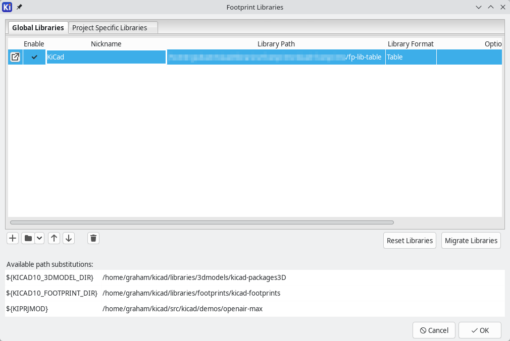
全局封装库表包含了始终可以使用的库列表,无论当前加载的工程是什么。该表保存在 KiCad 配置文件夹中的 fp-lib-table 文件中。该文件夹的位置 取决于正在使用的操作系统。
工程专用的封装库表包含了专门为当前加载的工程提供的库的列表。如果有任何工程专用的封装库,该表将保存在工程文件夹中的 fp-lib-table 文件中。
Many (or even all) of the loaded libraries may be contained in a nested library table, as shown in the screenshot above. To expand a nested library table and view its contents, press the ![]() button next to the nested library table entry. This opens the nested table in a new tab, as shown below.
button next to the nested library table entry. This opens the nested table in a new tab, as shown below.
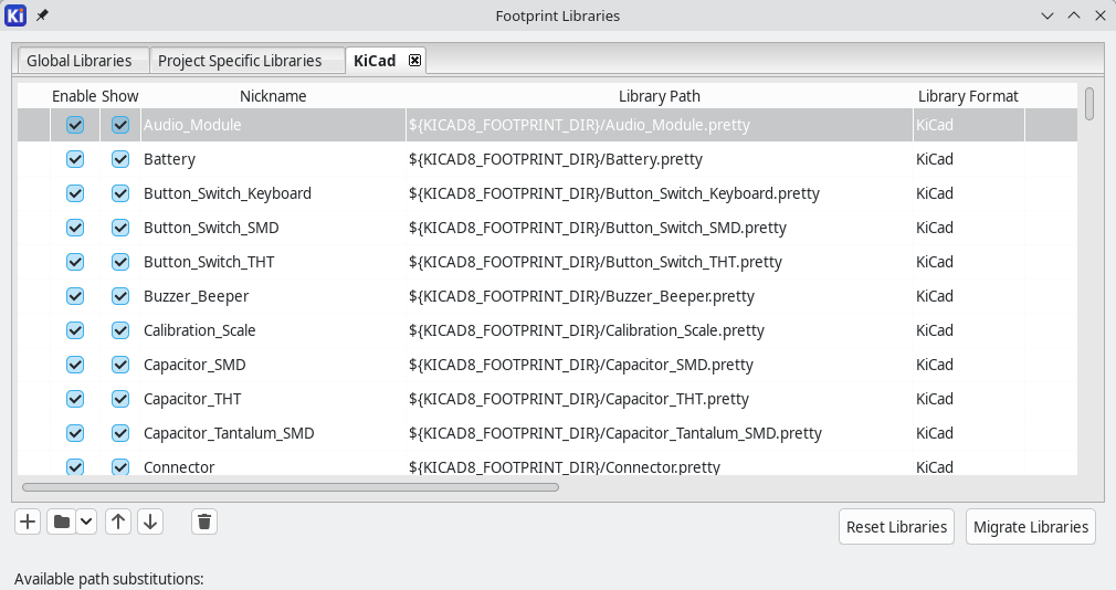
KiCad’s footprint library management system allows directly using many types of footprint libraries, including formats that are native to other non-KiCad EDA tools:
-
KiCad
.prettyfootprint libraries (folders with.prettyextension, containing.kicad_modfiles) -
KiCad Legacy footprint libraries (
.modfiles) -
Altium Designer (
.PcbLibor.IntLibfiles) -
CADSTAR PCB Archive (
.cpafiles) -
Eagle footprint libraries (
.lbrfiles) -
EasyEDA / JLCEDA Standard Edition (
.jsonor.zipfiles) -
EasyEDA / JLCEDA Professional Edition (
.elibz,.epro, or.zipfiles) -
GEDA libraries (folders containing
.fpfiles)
Non-KiCad footprint libraries, including KiCad Legacy footprint libraries, can be migrated to KiCad .pretty format using the Migrate Libraries button (see the migrating libraries section).
KiCad only supports writing to KiCad’s native .pretty format footprint libraries (and the .kicad_mod footprint files within them). All other footprint library formats are read-only. To modify a non-KiCad format footprint library, you must first convert it to KiCad format.
|
Library tables can also include other library tables, which are called nested library tables. When a nested library table is used, the libraries in the nested table are loaded as if they were included directly in the main table.
初始配置
The first time KiCad runs (or any time KiCad runs and no configuration is found), KiCad will guide you through creating a new configuration or importing a configuration from a previous version. This includes setting up a new footprint library table. This process is described in the Project Manager documentation.
You can reset your footprint library table to the default by clicking the Reset Libraries button in the footprint library table dialog.
| Resetting your footprint library table will permanently change your footprint library table on disk. |
The default footprint library table contains a single entry, which points to another footprint library table containing all of KiCad’s default footprint libraries. This nested library table is maintained as part of the KiCad libraries and is updated along with KiCad and its libraries. You should not edit it yourself.
| KiCad’s default footprint libraries are included in your library table via a nested library. This allows the list of default KiCad libraries to be updated when KiCad and its libraries are updated, without affecting your personal library configuration. Your personal library table configuration can be maintained between KiCad versions, while still allowing you to receive updates to the default libraries. |
Managing table entries
Footprint libraries can only be used if they have been added to either the global or project-specific footprint library table (or to a nested table included in either top-level table).
通过点击 ![]() 按钮并选择一个库或点击
按钮并选择一个库或点击 ![]() 按钮并输入库文件的路径来添加一个库。选定的库将被添加到当前打开的库表中(全局或工程专用)。可以通过选择所需的库条目并点击
按钮并输入库文件的路径来添加一个库。选定的库将被添加到当前打开的库表中(全局或工程专用)。可以通过选择所需的库条目并点击 ![]() 按钮来删除库。
按钮来删除库。
When an entry in the library table is itself another library table, you can open this nested table by clicking the ![]() button next to the nested table’s entry. This opens the nested table in a new tab, where you can see and edit the libraries included in the nested table. To add a nested library table, click the downwards arrow next to the
button next to the nested table’s entry. This opens the nested table in a new tab, where you can see and edit the libraries included in the nested table. To add a nested library table, click the downwards arrow next to the ![]() button, choose the Table library type, then browse to the table file.
button, choose the Table library type, then browse to the table file.
点击 ![]() 和
和![]() 按钮在库表中上下移动所选库。这并不影响在 "封装库浏览器"、"封装编辑器 "或 "添加封装工具 "中显示库的顺序。
按钮在库表中上下移动所选库。这并不影响在 "封装库浏览器"、"封装编辑器 "或 "添加封装工具 "中显示库的顺序。
Libraries can be made inactive by unchecking the Enable checkbox in the first column. Disabled libraries are still in the library table but do not appear in any library browsers and are not loaded from disk, which can reduce loading times.
点击范围内的第一个库,然后 Shift 点击范围内的最后一个库,可以选择一系列库。
每个库必须有一个独特的昵称:在同一个表中不允许有重复的库昵称。然而,昵称可以在全局和工程库表中重复。工程表中的库比全局表中的同名库更有优先权。
库的昵称不一定要与库的文件名或路径有关。冒号字符 (:) 不能用于库昵称或封装名称,因为它被用作昵称和封装之间的分隔符。
Each library entry must have a valid path. Paths can be defined as absolute, relative, or by path variable substitution.
The appropriate library format must be selected in order for the library to be properly read. The supported formats are listed above. Only KiCad format libraries (.pretty folders containing .kicad_mod files) can be saved. Other footprint library formats are read-only and must be converted to KiCad format before you can modify them.
有一个可选的描述字段,用于添加库条目的描述。选项字段目前不使用,所以添加选项在加载库时不会有任何影响。
Nested library tables
In addition to containing libraries, library tables can also contain other library tables. Library tables that are referenced by other library tables in this way are called nested library tables. Any libraries in a nested library table are loaded as if they were directly listed in the top-level library table.
Nested library tables let you separate groups of libraries into different library table files, then include all of the individual tables into the main top-level library table. This could be used, for example, to make a standard library table for your company, and share that table with everyone who needs it. Each user can then access the standard set of company libraries after they add the shared table as a nested library table in their own global table.
When KiCad is configured to its default library table configuration, the global library table contains a single entry, which is a nested library table. This nested table is part of KiCad’s default libraries and lists all of the KiCad default footprint libraries. When KiCad is updated, this nested table is also updated, which allows you to receive an updated list of KiCad’s default libraries without disturbing your personal library configuration.
Path variable substitution
The footprint library tables support path variable substitution, which allows you to define path variables containing custom paths to where your libraries are stored. PATH variable substitution is supported by using the syntax ${PATH_VAR_NAME} in the footprint library path.
By default, KiCad defines several path variables which are described in the project manager documentation. Path variables can be configured in the Preferences → Configure Paths… dialog.
Using path variables in the footprint library tables allows libraries to be relocated without breaking the footprint library tables, so long as the path variables are updated when the library location changes.
KiCad will automatically resolve versioned path variables from
older versions of KiCad to the value of the corresponding variable from
the current KiCad version, as long as the old variable is not explicitly
defined itself. For example, ${KICAD9_FOOTPRINT_DIR} will
automatically resolve to the value of ${KICAD10_FOOTPRINT_DIR} if there
is no KICAD9_FOOTPRINT_DIR variable defined.
|
${KIPRJMOD} is a special path variable that always expands to the absolute path of the current project directory. ${KIPRJMOD} allows libraries to be stored in the project folder without having to use an absolute path in the project library table. This makes it possible to relocate projects without breaking their project library tables.
Using the GitHub plugin
| KiCad 在 6.0 版本中取消了对 GitHub 库插件的支持。 |
Migrating footprint libraries to KiCad format
Non-KiCad format libraries, including legacy libraries (.mod files), are read-only. They need to be converted to KiCad format (.kicad_mod files in a .pretty folder) before you can save changes to them.
| As with most KiCad files, newer versions of KiCad can open older-format library files, but older versions of KiCad cannot read files once they have been saved by a newer version of KiCad. |
Libraries in other formats can be converted to KiCad libraries by selecting them in the footprint library table and clicking the Migrate Libraries button. Multiple libraries can be selected and migrated at once by Ctrl-clicking or shift-clicking.
Libraries can also be converted one at a time by opening them in the Footprint Editor and saving them as a new library.
Browsing footprint libraries
The Footprint Library Browser allows you to quickly examine the contents of footprint libraries. The Footprint Library Viewer can be accessed by clicking ![]() icon on the main Board Editor toolbar or with View → Footprint Library Browser.
icon on the main Board Editor toolbar or with View → Footprint Library Browser.
To examine the contents of a library, select a library from the list in the left hand pane. All footprints in the selected library will appear in the second pane. Select a footprint name to view the footprint.
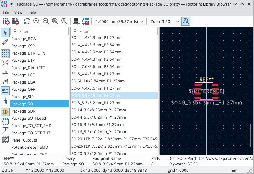
Double clicking the name of a footprint or using the ![]() button adds the footprint to the board.
button adds the footprint to the board.
The top toolbar contains the following commands:
|
Select previous footprint in library. |
|
Select next footprint in library. |
|
Zoom tools. |
|
Open footprint in 3D Viewer. |
|
Add the footprint to the board. |
|
Automatically zoom to fit each opened footprint. |
The left toolbar contains the following commands:
|
Selection tool (the default tool). |
|
Interactively measure the distance between two points. |
|
Turn grid display on/off. |
|
Switch between polar and Cartesian coordinate display in the status bar. |
|
Display/entry of coordinates and dimensions in inches, mils, or millimeters. Clicking the button toggles to the next unit, or you can choose a unit directly by expanding the palette (click and hold/drag). |
|
Switches the cursor crosshair between small, fullscreen, and 45-degree-rotated fullscreen. Clicking the button toggles to the next crosshair type, or you can choose a crosshair directly by expanding the palette (click and hold/drag). |
|
Show or hide pad numbers. |
|
Switch display of pads between filled and outline mode. |
|
Switch display of text between filled and outline mode. |
|
Switch display of graphic items between filled and outline mode. |
创建和编辑封装
A footprint is the physical interface between a component package and a circuit board. Footprints can contain:
-
Pads, which define how the component will be physically assembled onto the footprint. When a footprint is added to a board, tracks are routed to pads, and pads provide a magnetic snapping point for the router to connect the pad to a track. Pad shapes and layers are fully customizable, and pads can have plated holes, unplated holes, or no hole.
-
Graphic shapes and text for technical or aesthetic purposes. Graphics can be placed on physical layers (e.g. silkscreen or soldermask) or nonphysical layers. Graphic shapes can also be placed on copper layers, in which case they can make electrical connections.
-
3D models for mechanical CAD and visualization. 3D models are normally external files that footprints can link to, but they can optionally be embedded in footprints.
-
Metadata associated with the footprint.
Footprints in KiCad are organized into footprint libraries, which contain zero or more footprints. Generally footprints are logically grouped by footprint category, function, and/or manufacturer. Each library is a folder (usually ending in .pretty) containing a .kicad_mod file for each footprint in the library.
Footprint editor overview
KiCad provides a footprint editing tool that allows you to create footprint libraries; add, edit, delete, or transfer footprints between libraries; export footprints to files; and import footprints from files. The Footprint Editor can be launched from the KiCad Project Manager or from the Board Editor (Tools → Footprint Editor). You can also open the Footprint Editor from the a footprint in the board; in this way you can edit either the library copy or the board copy of that footprint in the editor.
| Editing the library version of a footprint will not affect any copies of that footprint that have been added to a board until the board copy is updated from the library. Conversely, editing the board version of a footprint will not affect the library version of a footprint or any other copies of that footprint in a board. |
The Footprint Editor main window is shown below. It has three toolbars for quick access to common features and a footprint viewing/editing canvas. Not all commands are available on the toolbars, but all commands are available in the menus.
| You can edit the toolbars' contents in the Toolbar page of the Footprint Editor Preferences. |
In addition to the toolbars, there are collapsible panels for the footprint tree and Properties Manager (not shown) on the left, and the appearance panel and selection filter on the right. The bottom of the window contains a message panel that shows details about the selected object.
Top toolbar
The main toolbar is at the top of the main window. It has buttons for the undo/redo commands, zoom commands, footprint/pad properties dialogs, and layer/grid management controls.
|
Create a new footprint in the selected library. |
|
Create a new footprint in the selected library using a footprint wizard. |
|
Save the currently selected footprint. |
|
Print the currently selected footprint. |
|
Undo last edit. |
|
Redo last undo. |
|
Refresh display. |
|
Zoom in. |
|
Zoom out. |
|
Zoom to fit footprint in display. |
|
Zoom to fit selection. |
|
Rotate selected item(s) counter-clockwise. |
|
Rotate selected item(s) clockwise. |
|
Mirror selected item(s) horizontally. |
|
Mirror selected item(s) vertically. |
|
Add the selected item(s) to a group. |
|
Remove the selected item(s) from a group. |
|
Edit the current footprint’s properties. |
|
Edit the selected pad’s properties. |
|
Open the current footprint’s datasheet. |
|
Run the footprint checker to test the current footprint for design errors. |
|
Edit a footprint in the current board in the footprint editor. |
|
Insert current footprint into the board. |
左侧工具栏显示控件
The left toolbar provides options to change the display of items in the Footprint Editor.
|
Turn grid display on/off. Note: by default, hiding the grid does not disable grid snapping. This behavior can be changed in the Display Options section of Preferences. |
|
Turn item-specific grid overrides on/off. |
|
Switch between polar and Cartesian coordinate display in the status bar. |
|
Display/entry of coordinates and dimensions in inches, mils, or millimeters. Clicking the button toggles to the next unit, or you can choose a unit directly by expanding the palette (click and hold/drag). |
|
Switches the cursor crosshair between small, fullscreen, and 45-degree-rotated fullscreen. Clicking the button toggles to the next crosshair type, or you can choose a crosshair directly by expanding the palette (click and hold/drag). |
|
Switches the line mode between free angle, 90 degree mode, and 45 degree mode for placement of new zones, graphical shapes, dimensions, and other objects. Clicking the button toggles to the next line mode, or you can choose a line mode directly by expanding the palette (click and hold/drag). You can also toggle between line modes using Shift+Space. |
|
Switch display of pads between filled and outline mode. |
|
Switch display of graphic items between filled and outline mode. |
|
Switch display of text between filled and outline mode. |
|
Switch the non-active layer display mode between Normal and Dim. Note: this button will be highlighted when the non-active layer display mode is either Dim or Hide. In both cases, pressing the button will change the layer display mode to Normal. The Hide mode can only be accessed via the controls in the Appearance Panel or via the hotkey Ctrl+H. |
|
Toggle display of library and footprint tree. |
|
Show or hide the Appearance and Selection Filter panels on the right side of the editor. |
|
Show or hide the Properties Manager panel on the left side of the editor. |
Right toolbar tools
Placement and drawing tools are located in the right toolbar.
|
Selection tool (the default tool). |
|
Add pad: click on the board to place a pad. |
|
Add rule area: Rule areas, formerly known as keepouts, can restrict the placement of items and the filling of zones and can also define named areas to apply specific custom design rules to. |
|
Note: Lines are graphical objects and are not the same as tracks placed with the Route Tracks tool. Graphical objects cannot be assigned to a net. |
|
Draw arcs: pick the center point of the arc, then the start and end points. By right clicking this button, you can change the arc editing mode between several editing modes that control how the arc center, endpoints, angle, and radius are maintained while the arc is edited. |
|
Draw rectangles. Rectangles can be filled or outlines. |
|
Draw circles. Circles can be filled or outlines. |
|
Draw graphical polygons. Polygons can be filled or outlined. Note: Filled graphical polygons are not the same as filled zones: graphical polygons cannot be assigned to a net and will not keep clearance from other items. |
|
Draw bezier curves: draw a bezier curve. Each curve is defined by its start and end points and two control points. Subsequent curves start as tangent to the previous one. Use Backspace to cancel the previous point. |
|
Add bitmap image for reference. Reference images are not included in fabrication outputs. |
|
|
|
|
|
|
|
Add dimensions. Dimension types are described in more detail below. |
|
Deletion tool: click objects to delete them. |
|
Anchor tool. Left-click to set the anchor position (origin) of the footprint. |
|
|
|
Interactively measure the distance between two points. |
Browsing, modifying, and saving footprints
The ![]() button displays or hides the list of available libraries, which allows you to select an active library. When a new footprint is created, it will be placed in the active library.
button displays or hides the list of available libraries, which allows you to select an active library. When a new footprint is created, it will be placed in the active library.
Clicking on a footprint name opens that footprint in the editor, and hovering the cursor over the name of a footprint displays a preview of the footprint.
After modification, a footprint can be saved in the current library or a different library. To save the modified footprint in the current library, click the ![]() button.
button.
To save the footprint changes to a new footprint, click File → Save As…. The footprint can be saved in the current library or a different library, and a new name can be set for the footprint.
To create a new file containing only the current footprint, click File → Export → Footprint…. This file will be a standard footprint library which will contain only one footprint.
The editor can also open footprints from the board. To edit a footprint from the board, right click a footprint in the Board Editor and select Open in Footprint Editor (Ctrl+E). Alternatively, you can open a board footprint by pressing the ![]() button in the Footprint Editor top toolbar and selecting the desired footprint.
button in the Footprint Editor top toolbar and selecting the desired footprint.
Editing and saving the board copy of a footprint will only update that footprint in the board; it will not update other copies of that footprint in the board, and it will not change the original library copy of the footprint. When you open the board copy of a footprint, the Footprint Editor displays an info bar that warns you the library copy will not be modified. You can click the link in this info bar to open the library version of the footprint instead, or press Ctrl+Shift+E.
Creating a new footprint library
You can create a new footprint library by clicking File → New Library…. This opens a file browser for you to choose a location and name for the new library. Footprint libraries are saved as a folder; the folder name is the library name plus the suffix .pretty.
The file browser also lets you choose whether the new library should be added to the global footprint library table or the project footprint library table. Libraries in the global library table will be available to all projects, while libraries in the project library table will only be available in the current project.
| The global and project footprint library tables are managed using Preferences → Manage Footprint Libraries…. This includes deleting and renaming footprint libraries. For more information about managing library tables, see the footprint library table documentation. |
After choosing a name, location, and library table, a new, empty library is created. When you create new footprints, you can save them in this library.
Creating a new footprint
To create a new footprint in the current footprint library, click the ![]() button or click File → New Footprint…. A new, untitled footprint will be created in the selected library. The new footprint is opened in the editor.
button or click File → New Footprint…. A new, untitled footprint will be created in the selected library. The new footprint is opened in the editor.
To set the name of the footprint, open its properties dialog (![]() button or E). The name will set the name of the footprint, which is used when assigning a footprint to a symbol, and is also used as the filename of the footprint file on disk.
button or E). The name will set the name of the footprint, which is used when assigning a footprint to a symbol, and is also used as the filename of the footprint file on disk.
The new footprint will be empty except for several default text items. The footprint contains two default (mandatory) footprint fields, Reference and Value. Reference contains the text REF**, which will be replaced with the reference designator of the footprint’s corresponding symbol when the footprint is added to the board. Value is initially set to Untitled, which can be changed, but this will also be updated with the contents of the corresponding symbol’s Value field when the footprint is added to the board. Finally, there is a footprint text item containing the string ${REFERENCE}, which is a text variable that will resolve to the value of the footprint’s Reference field once the footprint is on a board.
These items are centered on the footprint’s anchor (origin point), which is indicated with a magenta cross symbol. The anchor can be repositioned (changing the (0, 0) point for the footprint) by selecting the ![]() button and clicking on the new desired anchor position.
button and clicking on the new desired anchor position.
| Rather than manually creating a footprint, for some common footprints you can use a footprint wizard to create a footprint based on a set of parameters. |
Editing footprint properties
Footprints have a number of properties and metadata items that can be defined. These include text fields, attributes that can be set or not (such as Do Not Populate), clearance and zone connection settings, and 3D model paths. These are initially defined in the library copy of the footprint, but they can be modified on a per-instance basis once a footprint is added to a board. In other words, two copies of the same footprint on a single board can have their properties edited separately.
Some properties, namely text fields and attributes, will be automatically set for each footprint in a board based on the fields and attributes in the footprint’s corresponding schematic symbol. Fields and attributes are synced from symbols to footprints when you perform the Update PCB From Schematic action. They are also synced from footprints back to symbols when you perform the Update Schematic From PCB action.
To edit footprint properties, click the ![]() button to show the Footprint Properties dialog. You can also double click an empty spot in the editing canvas.
button to show the Footprint Properties dialog. You can also double click an empty spot in the editing canvas.
The most important settings are in the General tab. Here you can edit footprint fields as well as many basic properties for the footprint. Other tabs contain options for footprint layers, clearance overrides, pad connections including net ties and jumper pads, 3D models, and embedded files.
Footprint fields are explained in a separate section. The other settings in the General tab are:
-
Footprint name is the footprint’s name in the library. Footprints are identified by a combination of the library and footprint name. The footprint name is the same as the footprint’s filename on disk, and is also initially the same as the footprint’s
Valuefield. However, theValuefield can be edited in the footprint editor, and when a footprint is added to a board, itsValuefield will be updated with the value of the footprint’s corresponding symbol. -
Description is a description of the footprint. It should be human readable, but it is also used when searching for a footprint.
This description property is specifically a description of the
footprint. This is not to be confused with the Description field,
which will be set to the description of the footprint’s corresponding
symbol when the footprint is added to a board.
|
-
The keywords should contain additional terms related to the footprint. Keywords are primarily used, in combination with the footprint name and the
Descriptionfield, for searching for the footprint in the Footprint Chooser and the Footprint Editor. Those three items are also displayed when you select a footprint in the Footprint Chooser. -
Component type is one of SMD, Through hole, or Unspecified. A footprint’s type affects KiCad’s behavior in a few ways:
-
Footprint type can be used to filter footprints from component placement files as well as other exports, such as STEP files. Additionally, the footprint type is included as metadata in IPC-2581 exports.
-
Footprint 3D models can be shown and hidden in the 3D viewer based on their type. For example, SMD models can be hidden while through hole models are still displayed.
-
Footprints of different types are reported separately in the Board Statistics dialog.
-
DRC and the footprint checker will report footprints containing pads that do not match the parent footprint’s type, for example through hole pads in an SMD footprint.
-
-
Not in schematic, Exclude from position files, Exclude from bill of materials, and Do not populate set the default state of these attributes when the footprint is added to the board. These attributes are overridden by the value of the attributes in the footprint’s linked symbol.
-
If not in schematic is checked, KiCad will not expect the footprint to correspond to a symbol in the schematic. When updating a PCB from the schematic, KiCad will ordinarily remove footprints that don’t have corresponding symbols according to the delete footprints with no symbols setting. However, such footprints will not be deleted when they have not in schematic set.
-
If exclude from POS files is checked, KiCad will not include the footprint in component placement file exports.
-
If exclude from bill of materials is checked, the component will not be included in bill of materials exports in either the schematic or PCB editors. This attribute is synced to and from the footprint’s corresponding schematic symbol.
-
The do not populate attribute is primarily a schematic symbol attribute, and is synced to and from the footprint’s corresponding schematic symbol. Footprints with this attribute set can optionally be excluded from component placement file exports and some other types of outputs. These footprints can also be hidden in the 3D viewer.
-
Footprint pads
Pads are added to a footprint by clicking the ![]() button in the right toolbar, then clicking again in the desired location in the canvas. The tool continues adding new pads each time you click on the canvas until you cancel the tool (Esc). Each new pad has its pad number incremented by one relative to the previous pad number.
button in the right toolbar, then clicking again in the desired location in the canvas. The tool continues adding new pads each time you click on the canvas until you cancel the tool (Esc). Each new pad has its pad number incremented by one relative to the previous pad number.
You can configure basic surface-mount or through-hole pad shapes in the Pad Properties dialog. Some pads may require designing custom-shaped pads or postmachining/backdrilling.
KiCad also offers tools to help make it easier to design footprints containing many pads, including default pad properties, a pad renumbering tool, a pad table, and an array tool.
Editing pad properties
You can edit a pad after adding it by opening the pad’s properties dialog (E). These properties are also editable using the Properties Manager.
The most frequently edited properties of a pad are in the General tab. These include the pad’s position, geometry, and layer settings. Other tabs let you configure zone, thermal, and teardrop connections to the pad, electrical clearance and solder mask / paste expansion overrides, and post-machining and backdrilling.
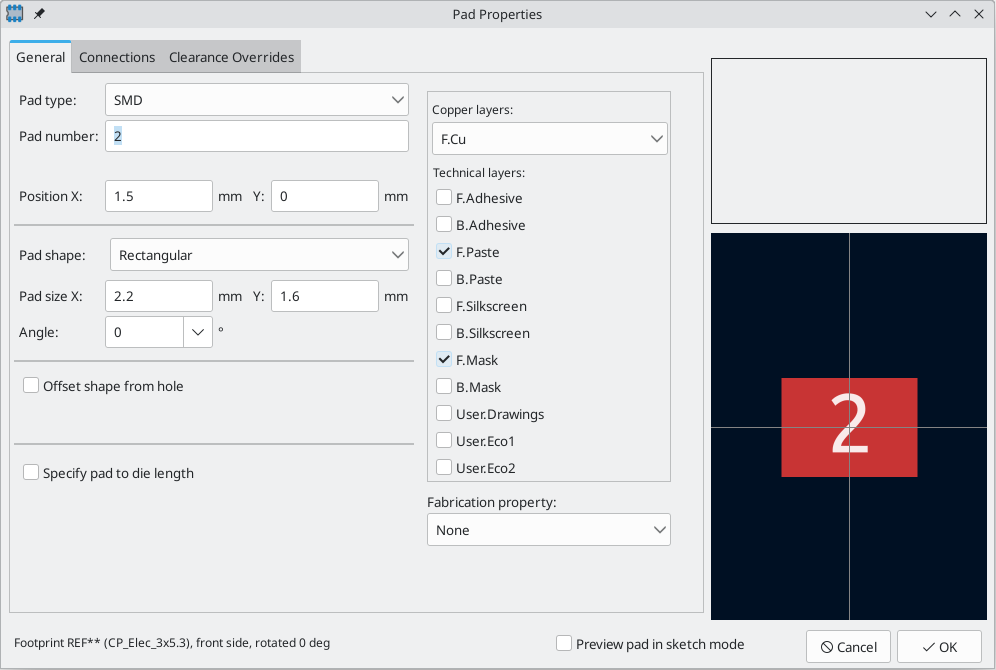
The pad settings in the General tab are:
Pad type controls which features are enabled for the pad.
-
SMD pads are electrically-connected and have no hole. In other words, they exist on a single copper layer.
-
Through-hole pads are electrically-connected and have a plated hole. The hole exists on every layer, and the copper pad exists on multiple layers (see Copper layers setting below).
-
Edge Connector pads are SMD pads that are allowed to overlap the board outline on the
Edge.Cutslayer. -
NPTH, Mechanical pads are non-plated through holes that do not have an electrical connection.
-
SMD Aperture pads are pads that have no hole and no electrical connection. These can be used to add specific designs to a technical layer, for example a paste or solder mask aperture.
铜层 设置控制哪些铜层将有一个与焊盘相关的形状。
-
For SMD pads, the options are
F.CuorB.Cu, controlling whether the pad sits on the front or the back of the board relative to the footprint’s location. In other words, if a pad is set to exist onB.Cuin its properties, and the footprint is flipped to the back of the board, that pad will now exist onF.Cu, because it also has been flipped. -
For through-hole pads, it is possible to remove the pad shape from copper layers where the pad is not electrically connected to other copper (tracks or filled zones). Setting the copper layers to connected layers only will remove the pad shape from any unconnected layers, and setting to
F.Cu,B.Cu, and connected layers will remove the pad shape from any internal unconnected layers. This can be useful in dense board designs to increase the routable area on internal layers.
技术层 复选框控制哪些技术层会有一个与焊盘形状相同的孔径。 默认情况下,焊盘在锡膏层和阻焊层上的孔径与铜层相匹配。
-
For SMD pads, the mask and paste apertures are on whichever outer layer matches the pad’s copper layer.
-
For through-hole pads, mask apertures are on both
F.MaskandB.Maskby default, with no paste apertures. The front and back mask and paste layers can be enabled or disabled independently.
| The solder mask expansion and solder paste margin values in the Clearance Overrides tab apply to all of the pad’s enabled mask and paste layers. |
The Pad number controls what the pad will be electrically connected to in the board. A pad has the same net connection as the pin with the same number in the corresponding schematic symbol.
Pad Position X and Y are the location of the center of the pad, relative to the footprint’s origin.
A pad’s diameter and hole size can be defined on a per-layer basis. This is also known as defining the pad’s padstack. The Padstack mode controls whether the pad shape is the same on all layers or whether individual layers are individually controlled.
-
In the Normal padstack mode, the pad’s diameter and hole size are the same on all layers.
-
In the Front/Inner/Back padstack mode, the pad’s diameter and hole size can be controlled separately for the front layer, the back layer, and the inner layers (the inner layers will all have the same settings). The Edit layer dropdown controls which layer (or group of layers) is currently being displayed and edited.
-
In the Custom padstack mode, the via’s diameter and hole size can be controlled completely independently on each layer. The Edit layer dropdown controls which layer is currently being displayed and edited.
Pad shape controls the basic shape of the pad. Pad shapes can be one of:
-
circular
-
oval
-
rectangular
-
trapezoidal
-
rounded rectangle
-
chamfered rectangle
-
chamfered with other corners rounded
-
custom (circular base)
-
custom (rectangular base)
Each pad shape has its own set of options; for example, rounded rectangles have settings for pad size X and Y, angle, corner size, and corner radius.
| The size of a pad can also be adjusted interactively in the canvas by dragging the editing handles at the pad corners. |
| Some components may require pads with unusual shapes that cannot be configured in this dialog. You can create custom pad shapes for such components. |
Through-hole and NPTH pads have a hole in addition to the pad itself. The hole shape can be circular or oval, with corresponding size controls. By default the pad is centered on the hole, but the pad can be offset relative to the hole if the offset shape from hole option is enabled (circular pads cannot be offset from the hole).
Fabrication properties are primarily used as metadata in Gerber X2 fabrication output, where the fabrication property is included as an aperture attribute for each pad. Some properties also affect DRC. The following fabrication properties are available:
-
BGA pad can only be applied to SMD pads, and only affects Gerber X2 output.
-
Fiducial, local to footprint and fiducial, global to board only affect Gerber X2 output.
-
Test point can only be applied to SMD or through hole pads, can only be applied to pads on outer layers, and only affects Gerber X2 output.
-
Through hole pads with the heatsink pad property are allowed in SMD footprints (PTH pads without this property cause a DRC violation when they are used in SMD footprints). It also affects Gerber X2 output.
-
The castellated pad property is for pads that intentionally intersect the board edge such that they will be bisected when the board is manufactured. Pads with this property are allowed to intersect the board edge and still be routed (it is otherwise a DRC error for a pad to intersect the board edge, which makes routing impossible). In STEP exports, pads with this property are clipped to the board edge. This property also affects Gerber X2 output.
-
Through hole pads with the mechanical property can be used in SMD footprints without causing a DRC violation. This can be used for mounting pads or other mechanical through hole pads in surface mount footprints. This is similar to the heatsink pad property, but does not affect Gerber X2 output.
-
The press-fit pad property is for pads designed to have component leads pressed into them without solder. This property only affects Gerber X2 output.
-
None is for pads for which none of the other fabrication properties apply. It has no effect.
Specify pad to die length: This setting allows a length to be associated with this pad that will be added to the routed track length by the track length tuning tools and the Net Inspector. This can be used to specify internal bondwire lengths for more accurate length matching, or in other situations where the electrical length of a net is longer than the length of the routed tracks on the board.
Specify pad to die delay: This setting is similar to the pad-to-die length, but for time-domain tuning. It allows a time delay to be associated with this pad that will be added to the routed track delay by the track length tuning tools.
Pad connections
The Connections tab of a pad’s properties contains settings for how pads connect to other objects, including settings for teardrops, zone connections, and thermal reliefs.
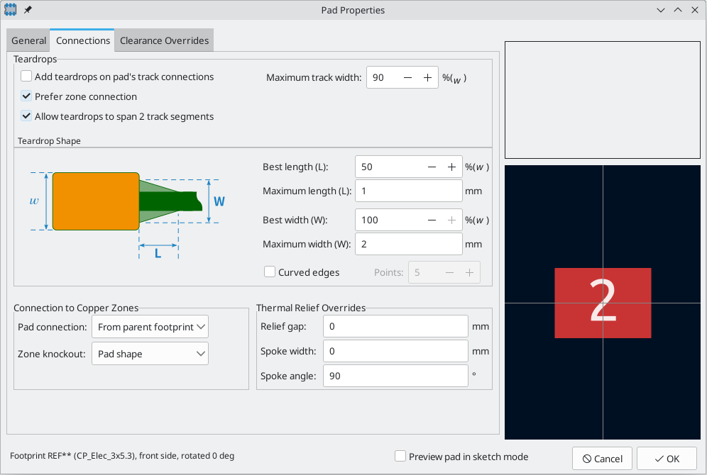
The Teardrops section contains settings controlling teardrop connections between tracks and the pad, if teardrops are used. Teardrop settings are explained in the teardrop documentation.
Pad connection controls whether the pad will have a solid, thermal relief, or no connection to the zone. Like the other overrides, this one may be set for an individual pad or for an entire footprint. The default setting for this control is From parent footprint, and the default footprint setting is to use the connection mode specified in the zone properties.
Zone knockout controls the behavior of the zone filler when the pad uses a custom shape rather than one of the default shapes. This can be used to achieve different results when using thermal reliefs and custom pad shapes.
Relief gap controls the length of the thermal spokes, or the gap between the pad’s shape and the filled copper area of the zone. This value is normally empty which will cause the relief gap to be inherited from the connecting zone’s settings.
Spoke width controls the width of the spokes generated when the zone connection mode is Thermal Relief. This value is normally empty which will cause the spoke width to be inherited from the connecting zone’s settings.
Prior to KiCad version 9, a relief gap or spoke width of 0 caused that value to be inherited.
In KiCad 9 and later, a relief gap or spoke width of 0 sets that value to 0, while a blank
value causes the value to be inherited.
|
Pad clearance overrides
The Clearance Overrides tab of a pad’s properties holds settings for pad-specific overrides to board clearance and mask/paste expansion.
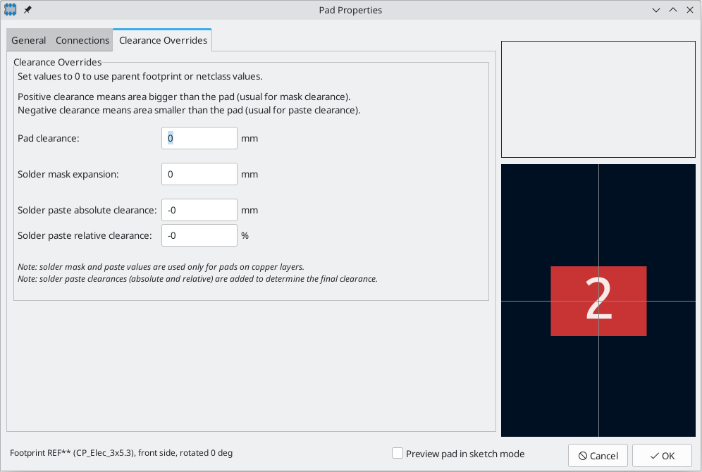
Pad clearance controls the minimum clearance between the pad and any copper shape (tracks, vias, pads, zones) on a different net. This value is normally empty which will cause the pad clearance to be inherited from any clearance override set on the footprint, or the board’s design rules and netclass rules if the footprint clearance is also empty.
Prior to KiCad version 9, a pad clearance of 0 caused the pad clearance value to be inherited.
In KiCad 9 and later, a pad clearance of 0 sets the clearance to 0, while a blank pad
clearance causes the clearance to be inherited.
|
The aperture appearing on any technical layer will have the same shape and size as the pad shape on the copper layer(s). In the PCB manufacturing process, the manufacturer will often change the relative size of mask and paste apertures relative to the copper pad size, but since this size change is specific to a manufacturing process, most manufacturers expect the design data to be provided with the apertures set to the same size as the copper pads. For specific situations where you need to oversize or undersize a technical layer aperture in the design data, you can use the settings here.
Solder mask expansion controls the size difference between the pad shape and the aperture shape
on the F.Mask and B.Mask layers. A positive number means the solder mask aperture will be larger
than the copper shape. This number is an inflation applied to all directions. For example, a
value of 0.1mm here will cause the solder mask aperture to be inflated by 0.1mm, meaning that
there will be an 0.1mm border on all sides of the pad and the solder mask opening will be 0.2mm
wider than the pad when measured along a given axis.
Solder paste clearance is a setting to specify the solder paste shape relative to the parent pad size
(the size difference between the pad shape and the aperture shape on the F.Paste and B.Paste layers).
This can be specified as an absolute offset from the pad edge (e.g. -0.1mm),
a value relative to the pad dimension (e.g. -5%),
or both (e.g. -0.1mm - 5%).
If it is 0 or blank, the solder paste aperture will be the same size as the pad.
Positive values mean solder paste aperture larger than the pad.
Negative values mean solder paste aperture smaller than the pad.
Pad post-machining and backdrilling
You can control post-machining and backdrill operations for pads in the Backdrill tab of the pad’s properties.
Post-machining and backdrilling are explained in their own sections.
自定义焊盘形状
For some footprints, the built-in pad shapes (round, rectangular, etc.) may not be sufficient. In these cases you can construct custom pads with arbitrary shapes using Pad Edit Mode. This mode lets you combine a basic pad with graphic shapes to build a new pad out of the compound shape.
To build a custom pad, first add a regular pad using the pad tool (![]() button). This base pad will become the custom pad’s anchor or snapping point, so be sure to place the pad in the exact location where you want tracks to attach to the pad. The shape and size of the pad do not matter, but the hole, if any, will remain in the final custom pad. In other words, a surface mount base pad will result in a surface mount custom pad, and a through hole base pad will result in a through hole custom pad. The custom pad’s number will be inherited from the base pad.
button). This base pad will become the custom pad’s anchor or snapping point, so be sure to place the pad in the exact location where you want tracks to attach to the pad. The shape and size of the pad do not matter, but the hole, if any, will remain in the final custom pad. In other words, a surface mount base pad will result in a surface mount custom pad, and a through hole base pad will result in a through hole custom pad. The custom pad’s number will be inherited from the base pad.
Next, enter Pad Edit Mode by selecting the base pad, right-clicking, and selecting Edit Pad as Graphic Shapes (Ctrl+E). Add graphic shapes as appropriate to create the desired pad shape. Shapes touching the base pad will be unioned together with the base pad to create the final pad shape.
You can exit Pad Edit Mode by right-clicking and selecting Finish Pad Edit, or pressing Ctrl+E again. When you exit pad edit mode, all shapes that touch the base pad will be combined with the pad. For example, when editing a surface mount pad on F.Cu, any shapes that are on F.Cu and touch the base pad will become part of the custom pad. Any shapes that do not overlap the base pad, or that are on a different layer, will remain separate. If the base pad is a through hole pad, overlapping shapes on F.Cu will be combined in the custom pad. Because through hole pads have the same pad shape on all copper layers, this shape will become part of the custom pad on all copper layers, not just F.Cu. For convenience, Pad Edit Mode dims the color of other pads and all shapes that are not contiguous with the base pad so that you can see which shapes will be included in the custom pad and which will not.
Custom pads can only contain a single base pad. Any additional pads that touch the base pad or the contiguous graphics, whether they have the same or different pad numbers as the base pad, will remain separate pads after the shapes are combined into the custom pad.
| If you would like to add multiple anchors (snapping points) to a custom pad, you can add additional separate pads on top of the custom pad. Create the custom pad as normal, containing the first snapping point, then add additional pads with the same number and place them overlapping the custom pad in the desired snapping locations. They will remain distinct pads and will not be combined with the custom pad, but they will act as additional pad anchors and will be electrically connected to the custom pad. |
To modify an existing custom pad, select it and enter Pad Edit Mode again. You can then continue to edit the component shapes to adjust the pad shape, or change the position of the base pad to adjust the pad anchor.
KiCad automatically chooses a size and location for showing the pad number over the pad. Particularly for unusually shaped pads, the automatically determined size and location may not be optimal. In these cases, you can manually specify a region in which KiCad should draw the pad number by adding a pad number box primitive. To add a number box, enter Pad Edit Mode and add a rectangular shape. In the Properties Manager for the rectangle, check the Number Box checkbox. The rectangle will then be shown as a wireframe, and when you exit Pad Edit Mode it will be used to draw the pad number.
In the board, KiCad will automatically add thermal spokes when connecting the pad to a zone. The thermal spoke settings are determined by the pad, footprint, and zone settings, and the thermal spokes by default connect to the pad anchor. You can override the default thermal spoke placement by adding thermal relief templates to the custom pad. To add a thermal relief template, enter Pad Edit Mode and add a line shape. In the Properties Manager for the line, check the Thermal Relief Template checkbox. In Pad Edit Mode, the line will then be shown as a wireframe, and it will not be shown outside of pad edit mode. If any thermal relief templates are present in the pad, KiCad will not automatically add additional spokes when filling zones; spokes will only be placed where there are thermal relief templates defined in the pad. Thermal relief templates only determine the spoke location: spoke width and relief gap are still defined in the pad, footprint, and/or zone properties, as normal.
Default pad properties
When you place a new pad, the new pad’s properties are copied from the default pad properties. Each time any pad is edited, the pad’s updated properties are stored as the default pad properties, so that new pads will match the properties of the most recently edited pad.
You can directly edit the default pad properties by selecting Edit → Default Pad Properties…, or choose an existing pad to represent the default by right clicking the pad and choosing Copy Pad Properties to Default. New pads will use that pad’s properties as their defaults until a new default is selected, either by editing another pad, editing the default pad properties, or manually copying a different pad’s properties to the default.
There are several ways to update existing pads with the properties of other pads. You can apply the default pad properties to an explicit selection of pads by selecting the desired target pads, right clicking, and choosing Paste Default Pad Properties to Selected from the right click context menu. You can also update other pads with a selected pad’s properties using Push Default Pad Properties to Other Pads…, also in the right click context menu.
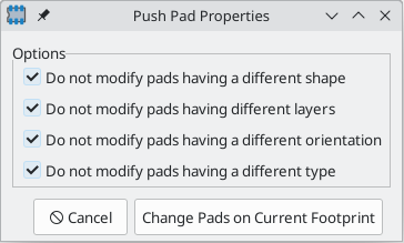
This tool has several options to filter which pads are targeted.
-
If do not modify pads having a different shape is selected, only pads with the exact same shape properties as the selected pad will be updated.
-
If do not modify pads having different layers is selected, only pads on the same layer(s) as the selected pad will be updated.
-
If do not modify pads having a different orientation is selected, only pads with the same orientation as the selected pad will be updated.
-
If do not modify pads pads having a different type is selected, only pads with the same pad type as the selected pad will be updated.
-
If no options are selected, all pads in the footprint will be updated.
Renumbering pads
You can quickly renumber existing pads using the Renumber Pads tool (Edit → Renumber Pads…).
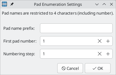
The tool has several options. Pads will be renumbered starting at the selected first pad number, and each subsequent pad will have its number incremented by the numbering step. You can also choose an optional pad name prefix which will be inserted before of the incrementing part of each pad number.
Once you click OK, you will be prompted to click on a pad, which will be assigned a new pad number based on the selected initial pad number and prefix. You can keep clicking on pads to assign them the next number in the sequence based on the selected numbering step. Double click on a pad to renumber that pad and end the sequence, or press Esc to discard the changes.
Pad table
Another way to edit pads is to use the Pad Table, which is accessible via the ![]() button. The Pad Table displays all of the pads in the footprint and their properties in a table view, so it is useful for making bulk pad changes. Any pad property can be edited by clicking on the appropriate cell.
button. The Pad Table displays all of the pads in the footprint and their properties in a table view, so it is useful for making bulk pad changes. Any pad property can be edited by clicking on the appropriate cell.
| Columns of the pad table can be shown or hidden by right-clicking on the header row and checking or unchecking additional columns. |
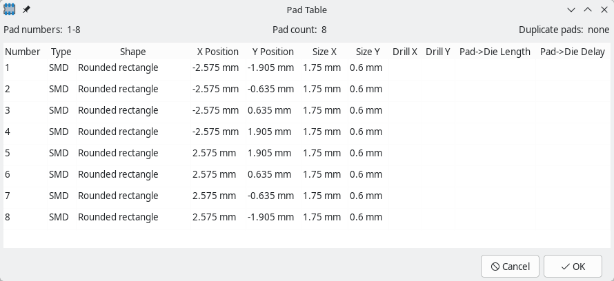
Pad arrays
You can create an array of pads from a source pad by right clicking the source pad and selecting Create from Selection → Create Array… (Ctrl+T).
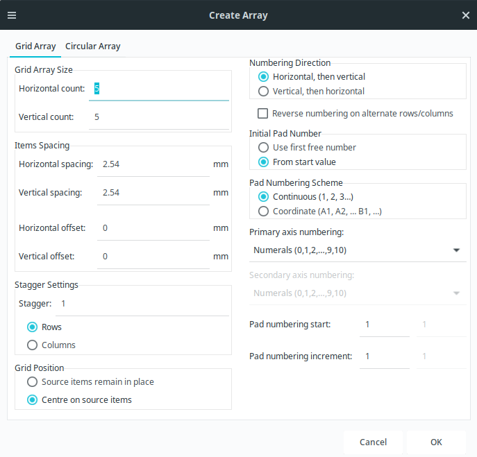
This array tool can also be used for creating arrays of other objects, as described in the PCB Editor documentation. For pads, however, there are additional options for controlling pad numbering.
If the Renumber pads option is enabled, pads will be renumbered when the array is created. For grid arrays, you can select a numbering direction, either horizontal, then vertical or vertical, then horizontal. If reverse numbering on alternate rows/columns is selected, the direction of increasing pad numbers will alternate from one row/column to the next.
The initial pad number in the array can either be the first unused pad number in the footprint (use first free number) or the specified pad numbering start value. After the first number, the pad numbering can either be continuous (1, 2, 3, …) or coordinate based, in other words, dependent on both the row and column (A1, A2, …, B1, …). In addition to the initial pad number (pad numbering start), you can specify a numbering step (pad numbering skip). For coordinate-based numbering, you can configure separate starting numbers and steps for each axis. You can select whether pad numbers use decimal digits (0-9), hexadecimal digits (0-F), the full alphabet, or the alphabet excepting certain ambiguous letters (I, O, S, Q, X, and Z).
Footprint graphics and text
Footprints can contain graphic shapes, text, and dimensions. These objects can be placed on nonphysical layers, like F.Fab or User.Drawings, or they can be placed on layers that will be part of the manufactured circuit board, such as Edge.Cuts or a silkscreen, soldermask, or copper layer. Objects on copper layers can make electrical connections.
Closed shapes on a footprint’s F.Courtyard and B.Courtyard layers will form the footprint’s front and back courtyard, respectively. A courtyard defines the physical extents of a footprint and limits where footprints are allowed to be placed in relation to other footprints. If a footprint’s courtyard overlaps another footprint’s courtyard, a DRC violation will be generated.
Shapes on a footprint’s Edge.Cuts layer will correspond to board edges on any PCB that includes the footprint. Closed shapes will result in cutouts, while unclosed shapes will result in unclosed edges. Unclosed edges must be closed in the full board design.
The buttons on the right toolbar can be used to create:
-
Lines (
, default hotkey Ctrl+Shift+L) -
Arcs (
, default hotkey Ctrl+Shift+A) -
Bezier curves (
, default hotkey Ctrl+Shift+B) -
Rectangles (
) -
Circles (
, default hotkey Ctrl+Shift+C) -
Polygons (
, default hotkey Ctrl+Shift+P) -
Text (
 , default hotkey Ctrl+Shift+T)
 -
Textboxes (
 )
) -
Tables (
 )
) -
Dimensions (
), of which several types are available
| You can customize the default style of newly-created text and shape objects in Preferences → Footprint Editor → Default Values. |
Graphical objects and their properties are described in more detail in the PCB Editor documentation.
Bulk editing footprint text and graphics
Properties of text and graphics can be edited in bulk using the Edit Text and Graphics Properties dialog (Edit → Edit Text & Graphic Properties…).
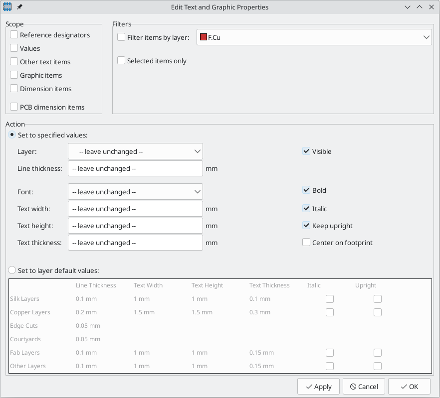
This dialog is described in more detail in the PCB Editor documentation.
Cleaning up footprint graphics
There is a dedicated tool for performing common cleanup operations on graphics, which is run via Tools → Cleanup Graphics….
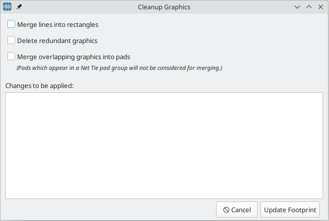
The following cleanup actions are available and will be performed when selected:
Merge lines into rectangles: combines individual graphic lines that together form a rectangle into a single rectangle shape object.
Delete redundant graphics: deletes graphics objects that are duplicated or degenerate.
Merge overlapping graphics into pads: merges graphic copper shapes that overlap pads into a custom pad.
Any changes that will be applied to the footprint are displayed at the bottom of the dialog. They are not applied until you press the Update Footprint button.
Footprint fields
Footprints contain multiple fields, which are named values containing information related to the footprint. Fields can be visible and shown on any board layer, or they can be hidden and only shown in the footprint’s properties. Some fields have special meaning to KiCad: Reference and Footprint are both both used by KiCad to identify schematic symbols and PCB footprints, for example. Other fields may contain information that is important for a design but is not interpreted by KiCad, like pricing or stock information for a part.
Any fields defined in a library footprint will be included in the footprint when it is added to a board. You can also add new fields to footprints in the board. Whether they are in the library footprint or not, these fields can then be edited on a per-footprint basis in the board. Symbol fields are also transferred to the board and added as fields in the corresponding footprint.
Footprint fields are different than graphic text. Fields are named, i.e.
they have both a name (Reference) and a value (R101), whereas
footprint text only has a value. Fields can be added to and deleted from
footprints in a board in the Footprint Properties dialog, while text items
can only be added to a footprint in the footprint editor. Fields are also
synced between footprints and their corresponding symbols in the
schematic. Before KiCad version 8.0, footprints did not have named fields,
only graphic text.
|
All library footprints are defined with four default fields which correspond to the default fields in library symbols: Reference, Value, Datasheet, and Description. These default fields cannot be deleted. The Reference field initially has the value REF**, while the Value field is initially set to the name of the footprint. In the board, the values of the four default fields will be set to the values of the matching fields in the footprint’s corresponding symbol.
The Description footprint field is the description of the symbol, not
the footprint, and will be overwritten by the value of the corresponding
symbol’s description. Footprints have a separate footprint description
property (not a field), which is specifically intended for a description
of the footprint.
|
Fields each have an associated layer, which determines which board layer the field will be placed on. Fields can also be visible or hidden.
To edit an existing footprint field, double-click the field, select it or hover and press E, or right-click on the field text and select Properties….
To add new fields, delete optional fields, or edit existing fields, use the ![]() icon on the main tool bar to open the Footprint Properties dialog. Fields can be arbitrarily named, but names starting with
icon on the main tool bar to open the Footprint Properties dialog. Fields can be arbitrarily named, but names starting with ki_, e.g. ki_description, are reserved by KiCad and should not be used for user fields.
Fields have a number of properties, each of which is shown as a column in the properties grid. Not all columns are shown by default; columns can be shown or hidden by right clicking on the grid header and selecting or deselecting columns from the menu.
Footprint layers
By default, footprints have a front copper layer (F.Cu), a back copper layer (B.Cu), and a third copper layer that represents all inner copper layers on any board the footprint is added to (Inner layers). However, you can customize this stackup by enabling the Use custom stackup option in the Layers tab of a footprint’s properties. When this setting is enabled, you must specify the exact number of copper layers contained in the footprint using the Copper layers dropdown. You can then customize any of these copper layers in the Footprint Editor, but if the footprint is added to a board with fewer copper layers, any items on the extra copper layers will be ignored.
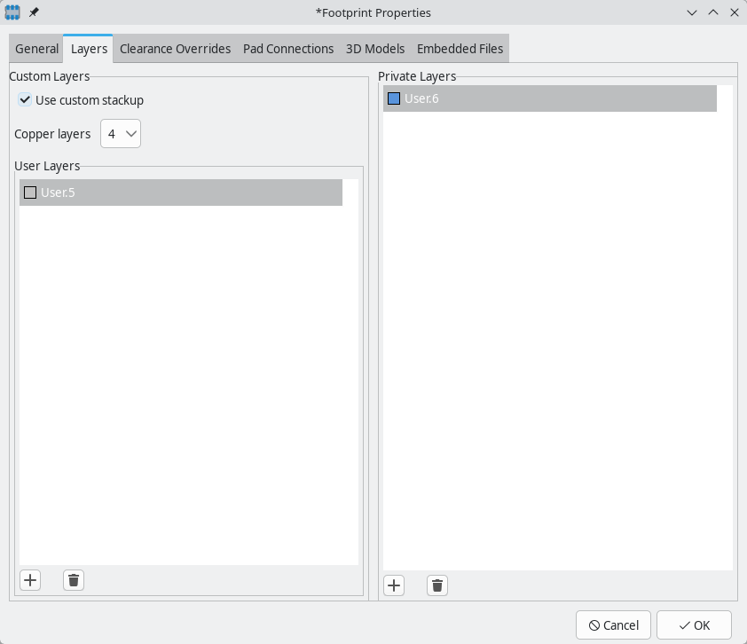
You can also add additional user (non-copper) layers using the User Layers table. Any layers configured in this table will be added to the footprint, and you can edit these layers like any other footprint layer. When the footprint is added to a board, these layers will be visible in the board editor if the board is configured to include those layers.
| You can globally configure the number of user layers in footprints, as well as their names, in the User Layer Names section of the Footprint Editor’s preferences. These user layers are shown in all footprints in addition to any layers configured in an individual footprint. |
Private footprint layers
Footprints can also have private footprint layers, which are layers that can be viewed and edited in the Footprint Editor but are never shown in the footprint when it is added to a board. Therefore any objects that are on private layers will not be visible in the PCB Editor or included in PCB fabrication outputs. This may be useful, for example, for notes or graphics that are of interest when drawing or editing a footprint but not needed at the board level.
Any of the existing User.* layers (User.Drawings, User.Comments, User.Eco1, User.1, etc.) can optionally be a private layer. To make a layer private, add a private layer in the Layers tab of the footprint properties dialog, then select the desired layer. Any objects on that layer will not be shown on the board.
Clearance overrides
The Clearance Overrides tab of Footprint properties holds settings for footprint-specific overrides to board clearance and mask/paste expansion.
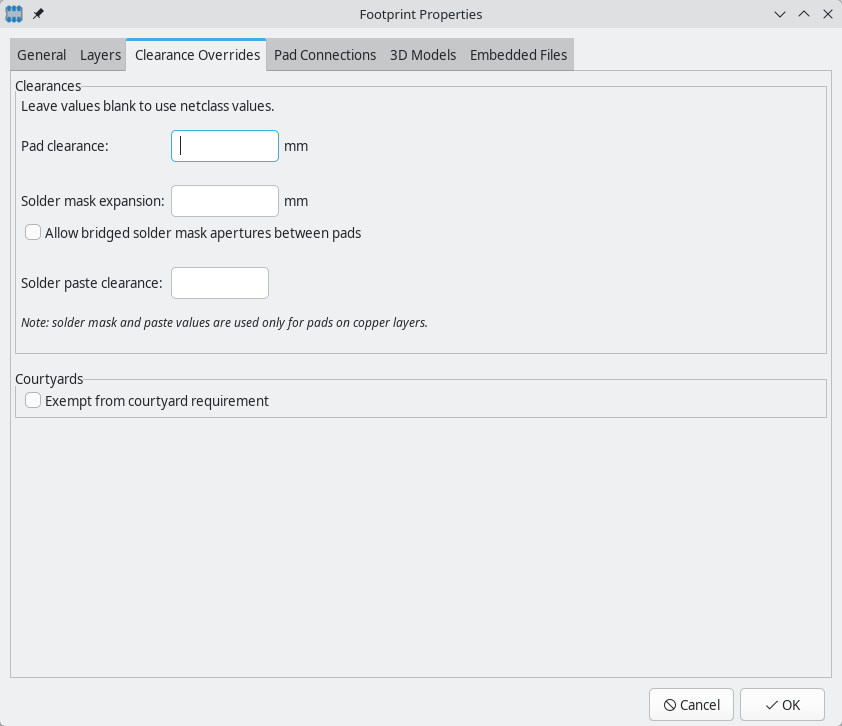
Pad clearance controls the minimum clearance between the footprint’s pads and any copper shape (tracks, vias, pads, zones) on a different net. This value is normally empty, which will cause the pad clearance to be inherited from the board’s design rules and netclass rules. This value can be overridden for individual pads by setting the pad’s clearance to a nonblank value.
Prior to KiCad version 9, a pad clearance of 0 caused the pad clearance value to be inherited.
In KiCad 9 and later, a pad clearance of 0 sets the clearance to 0, while a blank pad
clearance causes the clearance to be inherited.
|
The aperture appearing on any technical layer will have the same shape and size as the pad shape on the copper layer(s). In the PCB manufacturing process, the manufacturer will often change the relative size of mask and paste apertures relative to the copper pad size, but since this size change is specific to a manufacturing process, most manufacturers expect the design data to be provided with the apertures set to the same size as the copper pads. For specific situations where you need to oversize or undersize a technical layer aperture in the design data, you can use the settings here. These values can be overridden for individual pads by setting the pad’s expansion or clearance to a nonzero value.
Solder mask expansion controls the size difference between the pad shape and the aperture shape
on the F.Mask and B.Mask layers. A positive number means the solder mask aperture will be larger
than the copper shape. This number is an inflation applied to all directions. For example, a
value of 0.1mm here will cause the solder mask aperture to be inflated by 0.1mm, meaning that
there will be an 0.1mm border on all sides of the pad and the solder mask opening will be 0.2mm
wider than the pad when measured along a given axis.
Solder paste clearance is a setting to specify the solder paste shape relative to the parent pad size
(the size difference between the pad shape and the aperture shape on the F.Paste and B.Paste layers).
This can be specified as an absolute offset from the pad edge (e.g. -0.1mm),
a value relative to the pad dimension (e.g. -5%),
or both (e.g. -0.1mm - 5%).
If it is 0 or blank, the solder paste aperture will be the same size as the pad.
Positive values mean solder paste aperture larger than the pad.
Negative values mean solder paste aperture smaller than the pad.
If exempt from courtyard requirement is checked, the footprint will not trigger a DRC violation if it does not contain a courtyard. Without this attribute set, a footprint without graphics on the F.Courtyard or B.Courtyard layer will cause a "Footprint has no courtyard defined" DRC violation.
Clearance override hierarchy
Clearance, mask expansion, and paste margin values are resolved through a hierarchy of overrides. When a value is set at multiple levels, the most specific level takes precedence:
-
Pad-level override: A value set directly on an individual pad. This is the highest-priority override and applies only to that specific pad.
-
Footprint-level override: A value set in the footprint’s Clearance Overrides tab. This applies to all pads in the footprint that do not have their own pad-level override.
-
Board-level default: The global values configured in Board Setup → Solder Mask/Paste. These apply to all pads that do not have a footprint-level or pad-level override.
Pad connections, net ties, and jumper pads
The Pad Connections tab of Footprint Properties holds settings for how pads in the footprint connect to zones, whether the footprint can short two different nets (a net tie), and whether pads in the footprint are internally connected in the attached component (jumper pads).
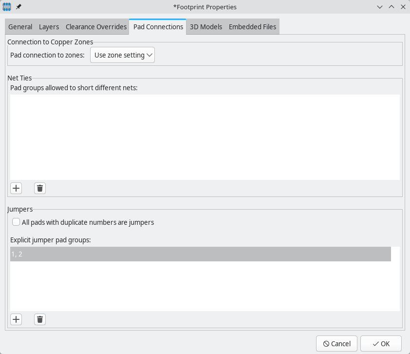
Pad connection to zones controls whether the footprint’s pads will have solid, thermal relief, or no connection to zones. The default setting for this control is From zone setting, which uses the connection mode specified in the connection zones' properties. The control in this tab sets the override for an entire footprint, but you can also override the setting for individual pads in each pad’s properties by setting the pad’s connection mode to a value other than From parent footprint.
Net ties
Footprints can act as net ties, where two separate nets are electrically connected by copper. Connecting nets together would normally causes a DRC error due to violating the clearance between two nets, but a footprint can be configured to short nets without causing a DRC violation. This can be used to connect multiple grounds at a specific location, to make kelvin sense connections to a component, or for other applications.
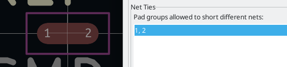
Net ties connect two or more nets in one contiguous region of copper. Each net in a net tie must have its own pad. Pads are not ordinarily allowed to short to other pads; to allow pads to be shorted in net ties, the shorting pads must be added to a net tie group. To create a net tie group, add the pad numbers of the shorting pads to the Net Ties table in the Pad Connections tab of the Footprint Properties dialog. For example, to allow pads 1 and 2 to short in a footprint, add a line to the table with the contents 1,2 or 1 2.
After creating a net tie group, the specified pads are allowed to be electrically shorted. Pads in net tie groups can be connected either by directly overlapping the pads or by adding a copper shape that overlaps both pads.
Footprints can contain multiple net tie groups. Each group can short two or more nets, but every group must remain electrically separate from other groups.
Jumper pads
You can configure a footprint to jumper some or all of its pads internally. Any jumpered pads will always have the same net; they are considered shorted together, even if they are not explicitly connected together in the schematic and PCB.
Footprint with jumper pads represent components that internally short together multiple pads. Examples of such components are wire jumpers, connectors with multiple connected shield pads, and switches with multiple shorted pads on each side of the switch.
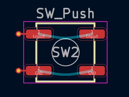
A footprint without jumpered pads. The ratsnest shows missing connections between same-numbered pads.
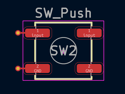
The same footprint in the same circuit with same-number pads jumpered (internally connected by the component). PCB connections between the same-numbered pads are no longer required.
Because KiCad considers the jumpered pads to be shorted by the component, you only need to connect to one of the shorted pads in the schematic and PCB.
| Jumper pads are different than net ties. A net tie allows copper to bridge two different nets, and each pad in the net tie has a different net. With jumper pads, each pad has the same net, and the electrical connection between jumper pads is assumed to be off-board in the attached component. |
You can configure jumper pads in the Pad Connections tab of a footprint’s Properties.
When the All pads with duplicate numbers are jumpers setting is enabled, all pads (and pins in the linked symbol) will be jumpered to the other pads with the same number. For example, all pads numbered 1 will be considered connected to each other.
You can also configure jumper pad groups for pads that don’t have the same number by adding Explicit pad jumper groups with the ![]() button. Enter multiple pad numbers separated by spaces or commas. A pad jumper group with the text
button. Enter multiple pad numbers separated by spaces or commas. A pad jumper group with the text 1 2 or 1, 2 will jumper together pads 1 and 2. A group with 3 4 5 or 3, 4, 5 will jumper together pads 3, 4, and 5.
| Like many other footprint properties, a footprint’s jumper pad settings are transferred from the linked symbol. You can configure a symbol’s jumper pins using the Symbol Editor. |
3D models
The 3D Models tab of Footprint Properties allows you to attach external 3D model files to a footprint and view the footprint in three dimensions along with any attached models.
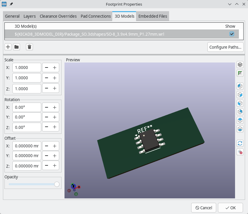
The main part of the window is a 3D preview of the footprint and any attached models. The buttons to the right of the preview let you enable or disable an orthographic projection (![]() ), show or hide the PCB model (
), show or hide the PCB model (![]() ), align the view to one of the six face-aligned perspectives (
), align the view to one of the six face-aligned perspectives (![]() ), and refresh the view (
), and refresh the view (![]() ). The bottom button (
). The bottom button (![]() ) lets you set the thickness of the PCB in the preview.
) lets you set the thickness of the PCB in the preview.
The top of the dialog lets you attach external models. Each added model will be shown in the footprint preview as well as in the full PCB 3D view when the footprint is added to a board. Footprint models can be in STEP, VRML, or IDF format. The models are specified as paths to the model files, which can contain path variables such as ${KIPRJMOD} or ${KICAD9_3DMODEL_DIR}. Click the Configure Paths button to configure path variables. If there is a problem loading a model file from the specified path, an icon in the leftmost column will indicate an error.
KiCad will automatically resolve versioned path variables from
older versions of KiCad to the value of the corresponding variable from
the current KiCad version, as long as the old variable is not explicitly
defined itself. For example, ${KICAD8_FOOTPRINT_DIR} will
automatically resolve to the value of ${KICAD9_FOOTPRINT_DIR} if there
is no KICAD8_FOOTPRINT_DIR variable defined.
|
| Many footprints in KiCad’s standard library do not yet have model files created for them. However, these footprints may contain a path to a 3D model that does not yet exist, in anticipation of the 3D model being created in the future. |
By default, models are added with their origin placed at the footprint’s origin, with no offset, scaling, or rotation. Offset, scaling, and rotation can be applied to a model using the controls to the left of the preview canvas. The model’s opacity can be adjusted using the opacity slider, and the model can be completely hidden by deselecting the show checkbox in the rightmost column of the model table.
Embedding files
External files can be embedded within a footprint. Embedding a file stores a copy of the file inside the footprint. The footprint can then refer to the embedded copy of the file instead of the external file, which makes the footprint more portable as it doesn’t rely on an external file, although the footprint’s filesize is increased as a result. In footprints this is especially useful for embedding 3D models. Files embedded in a footprint are deduplicated when the footprint is added to a board: if a file is embedded in a footprint, and multiple instances of that footprint are added to the board, only one copy of the file will be embedded, and all of the footprint instances will refer to the same embedded file. Files embedded in a footprint cannot be referred to in the parent board. File embedding is explained in more detail in the Board Setup documentation.
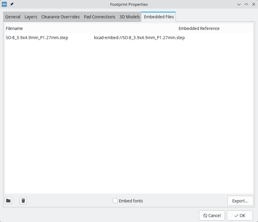
| You can add a 3D model to a footprint and embed it in one step. To do so, add a 3D model in the 3D Models, and enable the Embed File checkbox in the file browser while choosing a model. This embeds the file and automatically uses the embedded reference as the file path instead of the path to the external file. |
Rule areas
Rule areas, also known as keepouts, are footprint regions that can have specific DRC rules defined for them. Some basic rules are available that will raise DRC errors if certain types of objects are within the bounds of the rule area, but rule areas can also be used together with custom DRC rules to define complex DRC behavior that only applies within the rule area. A rule area in a footprint takes effect when the footprint is added to the board.
You can add a rule area by clicking the ![]() button on the right toolbar (Ctrl+Shift+K). Click on the canvas to place the first corner, which will show the Rule Area Properties dialog. After configuring the rule area appropriately, press OK to continue placing corners of the rule area. The rule area shape can be an arbitrary polygon; click on the starting corner or double click to finish placing the rule area.
button on the right toolbar (Ctrl+Shift+K). Click on the canvas to place the first corner, which will show the Rule Area Properties dialog. After configuring the rule area appropriately, press OK to continue placing corners of the rule area. The rule area shape can be an arbitrary polygon; click on the starting corner or double click to finish placing the rule area.
Rule areas are described in more detail in the PCB editor documentation.
Reference images
Just like in the PCB Editor, you can use reference images in the Footprint Editor to assist with your footprint designs. Footprint reference images are only shown in the Footprint Editor: they are not shown in the PCB Editor when a footprint is added to a board, and they do not appear in any fabrication outputs.
To add a reference image, use the ![]() button on the right toolbar and select the desired reference image file.
button on the right toolbar and select the desired reference image file.
Reference images are described in more detail in the PCB Editor documentation.
封装向导
KiCad provides a set of footprint wizards that can be used to create some common kinds of footprints based on a set of parameters. Wizards for the following types of footprints are provided:
-
BGA packages
-
QFN packages
-
QFP packages
-
SOIC, MSOP, SSOP, TSSOP, etc. packages
-
SIP and DIP packages
-
ZIP packages
-
ZOIC packages
-
FPC connectors
-
Micromatch SMD connectors
-
Circular pad arrays
-
Touch sliders
-
Mutual capacitance touch buttons
-
USS-39 barcodes
-
QR codes
To create a footprint using a footprint wizard, click the ![]() button and choose a footprint type from the list that appears.
button and choose a footprint type from the list that appears.
In the window that appears, fill out the parameters as appropriate. When the parameters are correctly filled out, press the ![]() button to transfer the generated footprint back into the footprint editor. Then you can make additional manual modifications and save the footprint as normal.
button to transfer the generated footprint back into the footprint editor. Then you can make additional manual modifications and save the footprint as normal.
In addition to the set of footprint wizards that KiCad provides, you can also create your own. For more information about creating new footprint wizards, see the Scripting section of the Advanced Topics chapter.
Checking footprints
The Footprint Editor can check for common issues in your footprints. Run the footprint checker using the ![]() button in the top toolbar.
button in the top toolbar.
Any footprint issues that are detected are listed in the dialog and displayed with arrow indicators in the editing canvas. Clicking on an issue in the dialog will focus on the issue in the canvas.
The footprint checker checks for:
-
Malformed or missing courtyards
-
Pads that don’t match the footprint’s type: footprints without any through hole pads should be set to the surface mount footprint type
-
Through hole pads without a hole
-
Plated through hole pads not on any copper layers
-
Plated through hole pads without a copper annulus
-
Plated through hole pads with a hole that isn’t fully within the pad
-
Surface mount pads on both the front and back
-
Surface mount pads with mismatched copper and paste/mask layers (front copper and back paste/mask, or vice versa)
-
Pads co-located with or too close to other holes
-
Collisions between silkscreen and solder mask openings
-
Pads that short to other pads outside of net tie groups
-
Nonexistent pads in net tie groups
-
Pads in that appear in multiple net tie groups
Multichannel layout
KiCad has a multichannel layout feature for replicating the layout of repetitive blocks of circuitry in a PCB design. This is useful for designs that contain multiple identical subcircuits, such as an audio mixer with many identical channels, a multi-output power supply with repeated regulation stages, or an LED driver board with identical per-channel circuitry. Instead of manually placing and routing each repeated block, you perform the layout for one block and then automatically replicate that placement and routing to all other matching blocks.
The multichannel layout workflow has three main stages:
-
Schematic setup: Designate which portions of the schematic represent the repeated parts of the circuit. Each repeated block is called a channel.
-
Rule area generation: Create placement rule areas on the PCB board to define the physical boundary of each channel.
-
Layout replication: Manually place and route one reference channel, then use the Repeat Layout tool to copy its placement and routing to all target channels.
Using the multichannel layout feature first requires you to designate which portions of the schematic represent the repeated parts of the circuit. You can use hierarchical sheets (with a repeated hierarchical sheet for each channel), component classes (with a unique component class assigned to the symbols in each channel), or named groups. Each channel will exactly correspond to the symbols (and their associated connections) in a single sheet, component class, or group.
For the layout, specially configured rule areas are drawn on the board and used to describe the physical location of each repeated channel. The automatic placement of footprints, routing, and other items is restricted to these placement rule areas. Each "channel" of the design corresponds to a single rule area. One rule area will be the reference rule area, which will be manually placed and routed. The other rule areas are the target rule areas, which will reuse the placement and routing from the reference rule area.
After setting up the placement rule areas for each channel and manually routing the reference channel, the Repeat Layout tool is used to copy the placement and layout from the reference rule area to the target rule areas.
KiCad includes a demo project, called multichannel, that demonstrates the use of the multichannel layout feature.
|
Multichannel design procedure: schematic
Designing a multichannel layout begins in the schematic. You need to specify which components (symbols) belong to each channel. Each channel in the schematic must be equivalent to the other channels. This means channels must match each other in the following ways:
-
each matched channel needs to have the same number of symbols
-
corresponding symbols in each channel need to have the same reference designator prefix (e.g.
RorU), although the full reference designators need to be unique as usual -
corresponding symbols in each channel need to have the same footprint
-
connections between symbols need to be equivalent in each channel
In the example schematic below, Channels 1, 2, 3, and 4 are equivalent and therefore can be used to share routing in a multichannel design. Even though the net connections are drawn differently in some channels, the underlying net connections are the same. The different symbols in Channel 2 and the different values in Channel 3 also do not break the equivalency. Footprint assignments are not shown in the image, but the symbols that correspond between channels must use the same footprints. In this example, this means that R1, R3, R5, and R7 each must use the same footprint, as must R2, R4, R6, and R8.
In contrast, Channels A and B are not equivalent to Channels 1-4, nor to each other. Channel A contains an extra parallel resistor not present in the other channels, and Channel B is missing a connection between the two resistors.
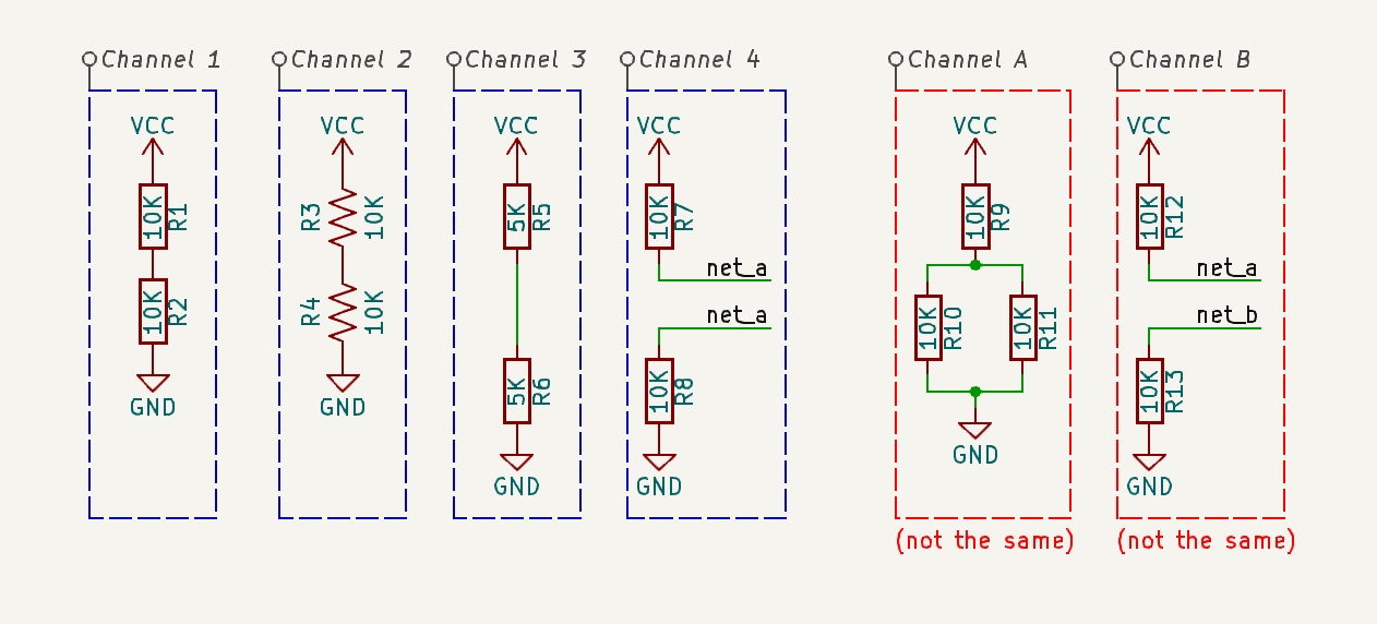
You can assign symbols to channels in three ways:
-
Hierarchical sheets: using hierarchical sheets, each channel is represented by a different sheet. Normally you will instantiate the same hierarchical sheet file multiple times, with one instantiation per channel. Each sheet instantiation needs to include all of the symbols for the corresponding channel, with no extra symbols.
-
Component classes: using component classes, each channel is represented by a different component class. Each component class needs to include all of the symbols for the corresponding channel, with no extra symbols. Component classes are shown in the previous schematic example.
-
Groups: using named groups, each channel is represented by a group of footprints on the board. This provides a more explicit way to define channels when hierarchical sheets or component classes are not suitable.
| Hierarchical sheets are the most common and convenient approach for multichannel designs. By instantiating the same sheet file multiple times, you guarantee that each channel has identical circuitry. The schematic editor automatically assigns unique reference designators to each instantiation. |
Multichannel design procedure: board
In the board, each channel is represented with a rule area with its rules configured for placement. You need to add a rule area for each channel. One rule area is the reference, containing manually placed and routed footprints. The other rule areas are targets and have the reference placement and routing copied to them. Placement rule areas, whether for reference or target channels, need the following settings configured in their properties:
-
The options in the Placement tab should be configured to select the hierarchical sheet, component class, or named group that contains the channel’s components.
-
The options in the Keepouts tab should typically be unselected, unless there is a specific type of item that needs to be excluded from the rule area.
-
The rule area’s layers should be set based on which layers are considered part of the channel. An item will be copied from the reference channel to a target channel only if the item’s layer is enabled in both the reference and target rule areas.
-
The area name is used to label the rule area when it is listed in the Repeat Layout dialog. While not strictly required, it will be hard for you to distinguish rule areas in the GUI unless each rule area has a unique name.
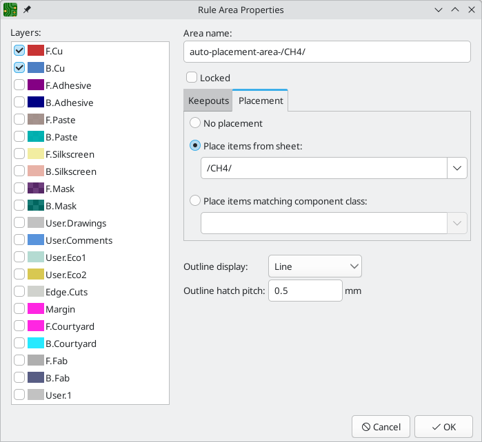
Generating placement rule areas
Placement rule areas can be manually created like any rule area, or they can be automatically generated by selecting Tools → Multi-Channel → Generate Placement Rule Areas…. This tool scans the design for hierarchical sheets, component classes, and named groups, then creates a placement rule area for each one you select. This is the fastest way to set up placement rule areas for a multichannel design.
| The tool allows you to generate a placement rule area for any sheet, component class, or named group, even if it is not intended to represent a channel in a multichannel design. It is your responsibility to select only the desired sheets, component classes, or groups. |
The Generate Multichannel Rule Areas dialog contains a tabbed notebook with three tabs:
-
Sheets: lists every hierarchical sheet path found on the board. Each row shows the sheet path and the sheet file name. Check the Generate checkbox for each sheet that represents a channel.
-
Component Classes: lists every component class assigned to footprints on the board. Check the Generate checkbox for each component class that represents a channel.
-
Groups: lists every named group on the board. Check the Generate checkbox for each group that represents a channel.
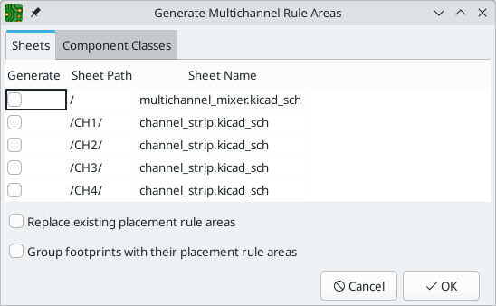
Below the tabbed source selection, the dialog has additional options:
| Option | Description |
|---|---|
Replace existing placement rule areas |
If enabled, the newly generated rule area for each channel will replace any rule areas that already exist for that channel. If disabled, channels that already have a placement rule area will be skipped. |
Group footprints with their placement rule areas |
If enabled, the newly generated rule area for each channel will be added to a group with all footprints associated with that rule area. This allows the target rule area and its associated items to be manipulated as a single entity. This option is disabled for group-based sources, because the footprints already belong to their respective groups. |
When you click OK, KiCad performs the following steps for each selected channel:
-
Queries the board for all footprints belonging to the sheet, component class, or group.
-
Computes a convex hull around those footprints with a small margin.
-
Rectifies the hull into an axis-aligned polygon using only 90-degree segments.
-
Creates a new rule area configured as a placement area, with the appropriate source type (sheet path, component class, or group name) recorded.
-
Sets the rule area layers to all copper layers.
-
If Replace existing is checked and a matching rule area already exists, the old rule area is removed.
-
If Group footprints is checked, a new group is created containing the rule area and all its associated footprints.
-
Names the generated rule area automatically using the pattern
auto-placement-area-<source>, where<source>is the sheet path, component class name, or group name.
After generating a rule area, you may want to change the configured layers to ensure all desired items in the reference channel get copied to the target channels.
| If generated rule areas are grouped with their footprints, you will need to enter the group (or ungroup the items) in order to edit the rule area. |
| After generating rule areas, enlarge the reference rule area to enclose all routing for the reference channel. Target rule areas will be resized automatically to match the reference when you run Repeat Layout. |
Repeating the layout
Once you have created rule areas for each channel and completed placing footprints and routing for the reference channel, you can use the Repeat Layout tool to copy the reference channel’s layout to the other channels. The tool is accessed from Tools → Multi-Channel → Repeat Layout….
The complete workflow is:
-
Select the reference rule area. Either select a placement rule area on the board before running the tool, or run the tool without a selection and you will be prompted to click on the reference rule area. The reference rule area is the one whose placement and routing you want to replicate.
-
Topology check. KiCad automatically finds all other placement rule areas on the board and checks whether their circuit topology matches the reference. This process attempts to find a one-to-one mapping of components and connections (an isomorphism) between the reference and each target. A progress indicator is shown for large designs.
-
Configure the Repeat Layout dialog. The dialog displays the results of the topology check and lets you select which targets to update and which items to copy.
-
Execute. Click OK to apply the reference layout to all selected target channels.
If a rule area is selected when the tool is run, that rule area will be used as the reference rule area. If no rule area is selected, you will be prompted to select a rule area. You can also select a group that contains a rule area, and the rule area within the group will be used. When the reference rule area is determined, a dialog will appear.
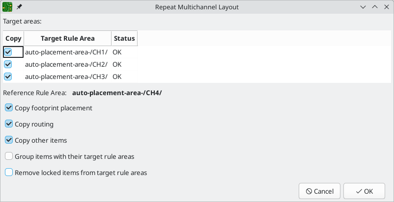
Target rule area table
The table at the top of the dialog controls which target rule areas will receive the layout from the reference channel. Each row represents one target rule area and shows the following columns:
| Column | Description |
|---|---|
Copy |
A checkbox controlling whether this target will receive the replicated layout. Targets whose topology matches the reference are checked by default. Targets with mismatches are unchecked and cannot be selected. |
Rule Area |
The name of the target rule area, as configured in its zone properties. |
Status |
Shows "OK" if the target channel’s topology matches the reference, or an error message describing the mismatch. Click the details icon (if present) to see a detailed breakdown of the mismatch reasons. |
The tool will only copy items to a target rule area if the target’s status is listed as "OK". If the status is not "OK", the target channel’s circuit topology cannot be matched to the reference channel; see the requirements for how channels need to match in the schematic for more information.
Repeat layout options
There are several options to control which items from the reference channel are copied to the selected target areas, and how those copied items are handled:
| Option | Description |
|---|---|
Anchor footprint |
If a footprint is selected in the dropdown, that footprint (and its equivalent in each channel) acts as an anchor for the channel. Each channel will be positioned and oriented relative to the channel’s anchor footprint. If no footprint is selected, each channel will be positioned relative to the center of the reference rule area. |
Copy footprint placement |
If enabled, the placement of footprints in the reference rule area will be replicated for footprints associated with the target rule area(s). Footprints are copied if they are enclosed by or intersect the reference rule area; they are not copied if they are fully outside. Footprints will only be copied if they are on a layer that is enabled in both the reference and target rule areas. |
Copy routing |
If enabled, any tracks and vias in the reference rule area will be copied to the target rule area(s). Routing is copied if it is fully enclosed by the reference rule area; it is not copied if it is partially or fully outside. Routing will only be copied if it is on a layer that is enabled in both the reference and target rule areas. Existing routing in the target rule areas is removed before the new routing is placed. |
Restrict to routing connected within the area |
A sub-option of Copy routing. When checked, tracks and vias will not be copied unless they share a net with a pad inside the reference rule area. This can be useful to prevent copying unrelated tracks that happen to pass through the rule area. |
Copy other items |
If enabled, any other items (zones, graphic objects) fully enclosed by the reference rule area will be copied to the target rule area(s). Items are copied if they are fully enclosed by the reference rule area; they are not copied if they are partially or fully outside. This means, for example, that a large copper zone that intersects a reference channel will not be copied to the target channels. Items will only be replicated if they are on a layer that is enabled in both the reference and target rule areas. |
Group items with their target rule areas |
If enabled, the items copied to a target rule area will be added to a group with that rule area. This allows the target rule area and its associated items to be manipulated as a single entity. |
Include locked items |
If enabled, items in the reference rule area will be copied even if they are locked, and items associated with target rule areas will be updated even if they are locked. If not enabled, locked items in the reference rule area will not be copied and locked items in the target rule area will not be updated or deleted to match the reference rule area. |
After clicking OK, the layout from the reference channel will be applied to the target channels. An info bar message confirms how many rule areas were updated. When the repeat layout is completed, each channel can be individually edited like any other part of the board design.
| You can run Repeat Layout multiple times as you refine your reference channel. Each run replaces the target channel contents with the current state of the reference channel. |
Topology matching
The core of the multichannel layout feature is the topology matching algorithm, which determines how components in the reference channel correspond to components in each target channel. Understanding how this matching works is important for diagnosing issues when channels fail to match.
How components are matched
KiCad analyzes the connectivity of both the reference and target channels. For each channel it catalogs:
-
Components: one entry per footprint, identified by its reference designator prefix (the letters before the numeric suffix, e.g.
RfromR1,UfromU3). -
Pins: one entry per pad on each footprint.
-
Connections: which pins share the same net.
Two components are considered the "same kind" if they share the same reference designator prefix. For hierarchical designs where references may include a channel identifier (such as TRIM_1.1 and TRIM_2.1), the algorithm detects a common prefix and treats the trailing channel-specific suffix as a channel identifier, so the components will still be matched.
The algorithm then searches for a one-to-one mapping (an isomorphism) of components in the reference to components in the target such that all pin connections are preserved. This means:
-
For every pair of connected pads in the reference channel, the corresponding pads in the target channel must also be connected.
-
The matching is based on actual net connectivity, not on reference designator numbers.
R1in the reference does not necessarily map toR1in the target — it maps to whichever resistor has the same connectivity pattern.
Tie-breaking for identical components
When multiple components in a target channel have identical connectivity (for example, a row of identical decoupling capacitors all connected between the same power and ground nets), the algorithm uses tie-breaking strategies to select the best match:
-
Symbol/sheet instance matching: if the reference and target components originated from the same hierarchical sheet instance, they are preferentially matched. This is the most reliable tie-breaker for hierarchical sheet designs.
-
Position-based proximity: components closer in physical position to their reference counterparts may be preferred.
Mismatch error details
When a target channel fails the topology check, the Status column in the Repeat Layout dialog shows an error summary. You can click the details icon in the rightmost column to view a detailed error dialog listing:
-
Which specific components could not be matched and why.
-
The total component count in the reference vs. the target area, if they differ.
-
A list of all components in each area for comparison.
See Troubleshooting multichannel layouts for common reasons that topology matching fails and how to resolve them.
Routing duplication details
When Copy routing is enabled, the Repeat Layout tool duplicates all tracks and vias from the reference rule area to each target rule area. Understanding how this process works will help you achieve clean results.
What is copied
The tool identifies routing in the reference rule area by testing whether each track or via on the board is enclosed by the reference rule area polygon. Items that are fully enclosed are candidates for copying. Items that only partially overlap or are fully outside the rule area are not copied.
For each copied item, the tool:
-
Duplicates the item (track segment or via).
-
Translates the duplicated item from the reference position to the target position, based on the offset between the rule area centers (or anchor footprints, if an anchor is set).
-
Rotates the duplicated item to match any orientation difference between the anchor footprints.
-
Reassigns the net of the duplicated item to the corresponding net in the target channel, using the component matching to look up which target pad connects to the same net.
Net reassignment
When a track or via is duplicated, it must be assigned to the correct net in the target channel. The tool does this by:
-
Finding which pads in the reference channel are connected to the same net as the original routing item.
-
Looking up those pads' parent footprints.
-
Finding the corresponding pads on the matched target footprints.
-
Assigning the target pad’s net to the duplicated routing item.
This means routing is automatically reassigned to the correct target-channel nets without any manual intervention.
Existing target routing
Before copying routing to a target area, the tool removes any existing routing within the target rule area that is on layers enabled in the target rule area. This ensures a clean copy without leftover routing from a previous iteration. If Restrict to routing connected within the area is enabled, only routing connected to pads within the area is removed.
Layer considerations
A routing item is only copied if its layer is enabled in both the reference and target rule areas. This means:
-
If the reference rule area includes layers
F.CuandB.Cu, but a target rule area only includesF.Cu, then only front-copper routing will be copied to that target. -
Inner copper layers must be explicitly included in both rule areas for inner-layer routing to be copied.
| Make sure all copper layers used by your routing are enabled in both the reference and target rule areas. A common issue is forgetting to add inner copper layers to the rule area layer set, which causes inner-layer routing to be silently skipped. |
When routing duplication fails
Routing duplication can produce unexpected results in several situations:
-
Routing extends outside the rule area: tracks that exit the reference rule area will not be copied. Make sure the reference rule area is large enough to enclose all routing for the channel, including any via fan-outs near the edge.
-
Net reassignment failure: if a track’s net cannot be mapped to a target channel net (for example, because it belongs to a global net that is not part of any channel), the duplicated track may retain the reference channel’s net. Enabling Restrict to routing connected within the area can help avoid copying such unrelated tracks.
-
Layer mismatch: if the reference routing uses a layer not enabled in the target rule area, those segments will be silently omitted.
Other item duplication
When Copy other items is enabled, zones and graphic objects (such as drawings, text, and dimensions) within the reference rule area are also duplicated to each target rule area. The same displacement and rotation transforms are applied.
Zones are duplicated with their net reassigned using the same component-match-based lookup used for routing. A zone is only copied if all of its layers are present in both the reference and target rule areas.
Graphic objects that are not connected (such as silkscreen text, board outlines, or fab layer drawings) are copied without net assignment. They must be on a layer enabled in both rule areas.
| Footprint text items (reference designators, values, and other footprint fields) are handled as part of footprint placement, not as standalone items. Their position, visibility, and attributes are updated to match the reference footprint’s fields when placement is copied. |
Step-by-step multichannel workflow
The following procedure summarizes the complete multichannel layout workflow from start to finish:
-
Design the schematic. Create the repeated circuit as a hierarchical sheet (or assign component classes / groups). Instantiate the sheet once per channel. Ensure all channels have identical circuit topology.
-
Import the netlist / Update PCB. Transfer the schematic to the PCB editor. All footprints for all channels will appear on the board.
-
Generate placement rule areas. Select Tools → Multi-Channel → Generate Placement Rule Areas…. In the dialog, check the sheets (or component classes, or groups) that correspond to your channels. Click OK.
-
Arrange the rule areas. Move each generated rule area to its desired position on the board. The footprints associated with each rule area do not need to be inside the rule area yet — that will happen during the repeat layout step.
-
Design the reference channel. Choose one rule area as your reference. Place all of its footprints inside the rule area and route the channel completely. Ensure the rule area boundary encloses all footprints, routing, and other items you want to replicate.
-
Enlarge the reference rule area if needed. The auto-generated rule area may be too small to enclose routing. Edit the rule area outline to include all routing, including via fan-outs and any local copper zones.
-
Run Repeat Layout. Select the reference rule area, then select Tools → Multi-Channel → Repeat Layout…. In the dialog:
-
Verify all target channels show OK status.
-
Select an anchor footprint if you want channels to be oriented relative to a specific component.
-
Enable Copy footprint placement, Copy routing, and Copy other items as desired.
-
Click OK.
-
-
Review the results. Inspect each target channel to verify that placement and routing were copied correctly. Run DRC to check for errors.
-
Iterate as needed. If you need to make changes to the reference channel’s layout, edit it and run Repeat Layout again. Target channels will be updated to match.
Troubleshooting multichannel layouts
Channels fail topology matching
If a target channel’s status shows an error instead of "OK" in the Repeat Layout dialog, the channel’s circuit topology does not match the reference. Click the details icon to see specifics. Common causes:
-
Missing or extra components: verify that each channel’s schematic sheet (or component class) contains exactly the same set of symbols. A common mistake is adding a decoupling capacitor to one channel but not the others.
-
Different reference designator prefixes: a component in the target channel has a different prefix than any component in the reference (e.g.
Rvs.C), so no pairing is possible. -
Different footprint assignments: corresponding symbols in different channels must use the same footprint. If
R1uses a 0402 footprint butR3uses a 0603, and they should correspond, the pad counts will differ and matching will fail. -
Different net connections: if a net is connected differently in one channel (e.g. a wire was accidentally deleted or connected to the wrong pin), the connectivity will differ.
-
Nested hierarchical sheets: child sheets within the channel sheet are included when querying components. Ensure that nested sheets are identical across channels.
Routing does not appear in target channels
-
Rule area too small: the most common cause. Routing outside the reference rule area boundary is not copied. Enlarge the reference rule area to enclose all routing.
-
Layer mismatch: ensure that all copper layers used by the routing are enabled in both the reference and target rule areas. Check the rule area properties on the Layers tab.
-
Unrelated routing filtered out: if Restrict to routing connected within the area is checked, tracks and vias whose net does not appear on any pad inside the rule area will be skipped. This is a net-based check, so a via that shares a net with a pad inside the area will be copied even if it is not physically routed to that pad. Uncheck this option if you need to copy routing on nets that have no pads inside the rule area.
-
Net reassignment to wrong net: if a track belongs to a global or shared net that is not unique to the channel (e.g. a power net), the duplicated track may retain the reference channel’s net instead of being reassigned. Enabling Restrict to routing connected within the area can help avoid copying such unrelated tracks.
Footprint placement is not copied
-
Footprint outside reference area: footprints must be enclosed by or intersect the reference rule area. Footprints fully outside the area are not copied.
-
Layer not enabled: a footprint is only copied if its layer is enabled in both the reference and target rule areas.
-
Locked footprints: if Include locked items is not checked, locked footprints in the reference area will not be copied, and locked footprints in the target area will not be moved.
Other items do not appear in target channels
-
Item not fully enclosed: zones and graphic objects must be fully enclosed by the reference rule area to be copied. A large copper zone that only intersects the rule area boundary will not be copied.
-
Zone layer mismatch: a zone is only copied if all of its layers are present in both the reference and target rule areas.
-
Locked items: if Include locked items is not checked, locked items in the reference area will not be copied and locked items in the target area will not be updated.
Target rule area shape is wrong
Target rule area outlines are automatically updated to match the shape of the reference rule area (translated and rotated to the target position). If a target rule area has a shape you did not expect, check the reference rule area’s outline — the target is a direct copy of it.
Tips for clean multichannel designs
-
Use hierarchical sheets with a single sheet file instantiated multiple times. This guarantees identical circuitry across channels.
-
Name your rule areas descriptively (e.g.
Channel 1,Channel 2) so you can easily identify them in the Repeat Layout dialog. -
Make the reference rule area generous in size. It is better to have extra space around routing than to accidentally clip routing at the boundary.
-
Route the reference channel completely before running Repeat Layout. Partial routing can be replicated, but it is easier to verify a complete channel.
-
Group items with rule areas for convenient manipulation. After replication, each channel’s components, routing, and rule area can be moved as a unit.
-
Run DRC after replication to catch any issues with the duplicated layout, such as clearance violations caused by different board areas or net assignment problems.
Design blocks
Design blocks allow you to save a portion of a schematic and/or layout and reuse it later. You can reuse design blocks within the same project or between different projects. Design blocks are saved and organized in design block libraries, much like symbols and footprints. A single design block can contain a schematic fragment, a layout fragment, or both.
When you instantiate a schematic design block in a schematic, the saved schematic fragment is inserted into the current schematic, either in the current sheet or in a new subsheet. Instantiating a layout design block directly adds saved board fragment to the board. If a design block contains both schematic and layout fragments, you can apply the saved layout to the footprints that correspond to the symbols in the schematic fragment.
Typically, design blocks are created first as a schematic fragment, with layout added later. Reusing schematic fragments in design blocks is covered in the Schematic Editor manual.
To use layout design blocks, first show the Design Blocks panel by clicking View → Panels → Design Blocks. This opens a docked panel on the right side of the schematic editor. To close the panel, use the same menu entry again, click the close button in the top right of the panel, or right click in the panel and choose Hide Library Tree.
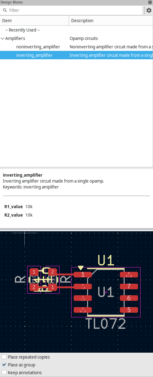
The Design Blocks panel lets you create design block libraries and create, edit, and place design blocks in the PCB.
Creating and managing design blocks
Design blocks are saved in design block libraries, so you need to add a library before you can save any design blocks.
Creating a new design block library
To create a new library, right click in the library tree and select New Library…. This opens a file browser for you to choose a location and name for the new library. Design block libraries are saved as a folder; the folder name is the library name plus the suffix .kicad_blocks.
The file browser also lets you choose whether the new library should be added to the global design block library table or the project design block library table. Libraries in the global library table will be available to all projects, while libraries in the project library table will only be available in the current project.
| The global and project design block library tables are managed using Preferences → Manage Design Block Libraries…. This includes deleting and renaming design block libraries. The design block library tables behave in the same way as the symbol and footprint library tables. For more information about managing library tables, see the footprint library table documentation. |
After choosing a name, location, and library table, a new, empty library is created. When you create new design blocks, you can save them in this library.
Creating a new design block
In the PCB Editor, design blocks can be created either from the entire contents of a board or from a selection of board objects. To create and save a new design block, select the desired source objects, either by opening the desired sheet or selecting the objects in the editing canvas. Then right click the design block library that will contain the block and select Save Board as Design Block… or Save Selection as Design Block… as appropriate.
| To save a layout fragment to an existing design block, including a design block that contains a schematic but no layout fragment, don’t create a new design block. Instead, update the existing design block. |
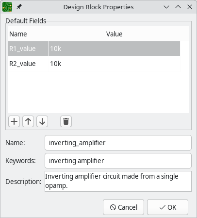
This brings up the Design Block Properties dialog, where you can edit the properties of the new design block.
-
Name: this is the name of the new design block, which is shown in the library tree and the preview pane. It is also used when filtering design blocks with the filter textbox. When design blocks are added as a group or as a schematic sheet, this is the default name of the new group or sheet.
-
Keywords: these are space-separated keywords describing the design block. They are displayed in the design block preview pane and used when filtering design blocks with the filter textbox.
-
Description: this is a description of the design block, which is shown in the library tree and the preview pane. It is also used when filtering design blocks with the filter textbox.
-
Default Fields: these are key/value pairs which are included as hierarchical sheet fields when the design block’s schematic is placed as a sheet. Fields are ignored when the design block is not placed as a sheet.
You can edit a design block’s properties after creating it by right clicking the design block in the design block library tree and selecting Properties….
Updating an existing design block
To update the layout of an existing design block, first place the design block you want to modify, then edit the layout as desired. If the design block exists but does not contain a layout portion, place the design block in the schematic, update the pcb from the schematic to add the linked footprints to the board, then edit the layout as desired.
When the layout changes are complete, save the modified layout to the original design block: select the board elements you want to save as the design block, then right click the name of the design block you want to modify and click Update Design Block from Selection. The existing contents of the design block are replaced by the selection.
Depending on how the design block was placed in the schematic, there are several other possible ways to save the modified schematic into the design block. If the current board only contains what you want to save into the design block, you can right click the name of the design block in the Design Block panel and click Update Design Block from Board. The existing contents of the design block are replaced by everything in the board. If the design block was placed as a group, you can right click the group in the canvas and choose Save to Linked Design Block.
Using design blocks in a board
There are two ways to use layout design blocks in a board, which are useful in different situations.
-
Design blocks can be directly added to a board, in the same way that schematic design blocks are directly added to a schematic. When a design block is added this way, its contents are not associated with any symbols from the schematic. This can be useful to add footprints or other board items in a predetermined arrangement when those items do not correspond to anything in the schematic. For example, mounting holes in a particular pattern could be added this way.
-
If a design block was used in the schematic, you can go through the normal Update PCB from Schematic flow to add the schematic design block’s symbols' assigned footprints to the board, then apply the design block’s saved layout to those footprints. This lets you reuse both a schematic fragment and its linked layout.
Both ways are explained in more detail below.
Directly placing design blocks in a board
To directly place a layout design block in a board, without any schematic symbols that correspond to the contents of the layout design block, you can place the layout design block using the Design Blocks panel.
The Design Blocks panel contains a library tree that lists your design block libraries and the design blocks contained in each library. Each library can be expanded or collapsed to show or hide the design blocks in that library. There is a Recently Used pseudo-library at the top of the tree that contains any design blocks that you have recently placed. You can pin any libraries to the top of the list by right clicking the library and selecting Pin Library.
You can filter design blocks by their name, description, and keywords using the filter textbox at the top of the Design Blocks panel. By default, matches are sorted by best match, but you can change to sorting alphabetically by selecting Sort Alphabetically under the ![]() menu.
menu.
When you select a design block in the library tree, the design block’s name and metadata are displayed below the library tree along with a graphical preview of the design block. The metadata includes the block’s description and keywords.
To add a design block to the schematic, double click it in the library tree or right click a design block and select Place Design Block.
There are several options controlling how the design block is placed:
-
If the Place repeated copies checkbox is enabled, KiCad will begin placing the design block again when you finish placing the previous block. To cancel placing the next block, press Esc or right click and select Cancel.
-
If the Place as group checkbox is enabled, the contents of the design block will be added to a group in the board, and the group’s library link will be set to point to the source design block and library. It is not required to place design blocks as a group, but some design block functionality is not available unless the design block is grouped. See the Grouped design blocks section for more information.
-
If the Keep annotations checkbox is enabled, KiCad will insert the design block without changing the footprint annotations as defined in the saved design block. If it is not enabled, KiCad will clear the footprint annotations while inserting the design block.
Once placed in a schematic, the contents of a design block behave the same as any other schematic objects and can be edited, moved, deleted, etc. exactly as if they were added to the schematic normally.
Applying layouts to design blocks from a schematic
If you want to reuse a layout on some footprints that are linked to symbols in your schematic, you can use design blocks to achieve this. You will need a design block that contains both schematic and layout fragments. After you add the design block in the schematic, you can apply the saved layout to the corresponding footprints.
| Also consider the multichannel tool as an alternative workflow for reusing layout within a project. |
The process for applying a design block’s saved layout is as follows:
-
Create a design block that contains both schematic and layout components.
-
Add the design block to the schematic. Make sure to place the schematic design block as a group.
-
Update the PCB from the schematic. Make sure to enable the Group footprints based on symbol group option. This adds footprints to the board corresponding to the symbols in the schematic design block and groups them together. The group is set up with a library link that points to the correct design block.
-
In the PCB Editor, select the group of footprints that corresponds to the schematic design block. Right click it and choose Apply Design Block Layout. This rearranges the footprints according to the design block layout, draws tracks between pads as appropriate, and adds any other contents from the design block layout such as graphics or text. The new items are also added to the group.
Grouped design blocks
When you place a design block in a board, you have the option to place the block as a group. You also have the option to group the design block’s board contents when transferring a design block from the schematic, as long as the design block was also grouped in the schematic. In addition to keeping the design block together as a single unit, some design block features can only be used if the design block’s contents are grouped. In particular, design blocks must be grouped in both the schematic and PCB if you plan to apply a layout to the design block in the PCB.
The following design block features can be used when a design block is grouped:
-
Place additional instances of a design block by right clicking the grouped design block and clicking Place Linked Design Block.
-
Update the library version of a design block to match a design block in the PCB by right clicking the grouped design block and clicking Save to Linked Design Block.
-
Copy the schematic group to the PCB, grouping the footprints corresponding to the design block’s symbols, by updating the PCB from the schematic.
-
Apply a design block layout to the footprints in a design block by right clicking the grouped footprints in the PCB and clicking Apply Design Block Layout.
-
As an alternative workflow to applying the layout saved in a design block, use the multichannel tool to repeat a layout from one group to another. With this workflow, you can place a design block as a group in the schematic, transfer the group to the PCB, manually perform the layout for one design block’s group, and then use the multichannel tool to replicate the layout of the first group to the other groups.
When starting from a schematic design block, the easiest way to group a design block is to enable the Place as group checkbox when you place the design block in the schematic. Then transfer the group to the PCB while updating the PCB from the schematic by enabling the Group footprints based on symbol groups option.
When directly placing a layout design block, you can enable the Place as group checkbox when you place the design block in the PCB.
If you didn’t place a design block as a group, but want to group it later, that’s also possible. First, select all of the contents of the design block, then group them. It is important that the group includes exactly the contents of the design block, with no missing or extra items. In the group’s properties, set the Library link so that it matches the design block’s name and library, in the format <library>:<block>. For example, the library link for the inverting_amplifier design block in the amplifiers design block library would be amplifiers:inverting_amplifier.
高级主题
配置和自定义
KiCad PCB 编辑器有多种偏好设置,可通过偏好设置对话框进行配置。和 KiCad 的所有部分一样,PCB 编辑器的偏好设置存储在用户配置目录中,并且在 KiCad 的小版本之间是独立的,以允许多个版本的偏好设置分别运行。
偏好设置对话框的第一部分(通用、鼠标和触摸板以及快捷键)是所有 KiCad 程序共享的。这些部分在 KiCad 手册中的 "常规偏好设置" 部分有详细描述。
显示选项
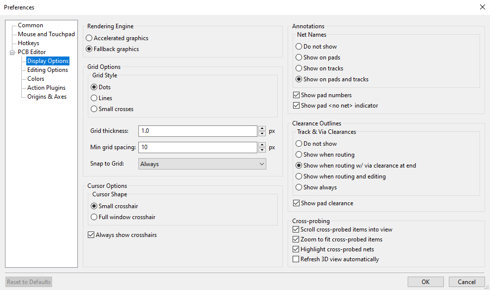
Rendering Engine: Controls if Accelerated graphics or Fallback graphics are used.
Grid style: Controls how the alignment grid is drawn.
Grid thickness: Controls how thick grid lines or dots are drawn.
Min grid spacing: Controls the minimum distance, in pixels, between two grid lines. Grid lines that violate this minimum spacing will not be drawn, regardless of the current grid setting.
Snap to grid: Controls when drawing and editing operations will be snapped to coordinates on the active grid. "Always" will enable snapping even when the grid is hidden; "When grid shown" will enable snapping only when the grid is visible.
| 按住 Ctrl 可以暂时禁用网格捕捉。 |
Cursor shape: Controls whether the editing cursor is drawn as a small crosshair or a full-screen crosshair (a set of lines covering the entire drawing canvas). The editing cursor shows where the next drawing or editing action will occur and will be snapped to a grid location if snapping is enabled.
Always show crosshairs: Controls whether the editing cursor is shown all the time or only when an editing or drawing tool is active.
Net names: Controls whether or not net name labels are drawn on copper objects. These labels are guides for editing only and do not appear in fabrication outputs.
Show pad numbers: Controls whether or not pad number labels are drawn on footprint pads.
Show pad <no net> indicator: Controls whether or not pads with no net are indicated with a special marker.
Track clearance: Controls whether or not clearance outlines around tracks and vias are shown. Clearance outlines are shown as thin shapes around objects that indicate the minimum clearance to other objects, as defined by constraints and design rules.
Show pad clearance: Controls whether or not clearance outlines around pads are shown.
Center view on cross-probed items: When the Schematic and PCB Editors are both running, controls whether clicking a component or pin in Eeschema will center the PCB Editor view on the corresponding footprint or pad.
Zoom to fit cross-probed items: Controls whether the view will be zoomed to show a cross-probed footprint or pad.
Highlight cross-probed nets: Controls whether or not nets highlighted in Eeschema will be highlighted in the PCB Editor when the highlight tool is activated in both tools.
编辑选项
Flip board items L/R: Controls the direction board items will be flipped when moving them between the top and bottom layers. When checked, items are flipped Left-to-Right (about the Vertical axis); when unchecked, items are flipped Top-to-Bottom (about the Horizontal axis).
Step for rotate commands: Controls how far the selected object(s) will be rotated each time the Rotate command is used.
Allow free pads: Controls whether or not the pads of footprints can be unlocked and edited or moved separately from the footprint.
Magnetic points: This section controls object snapping, also called magnetic points. Object snapping takes precedence over grid snapping when it is enabled. Object snapping only works to objects on the active layer. Hold Shift to temporarily disable object snapping.
Snap to pads: Controls when the editing cursor will snap to pad origins.
Snap to tracks: Controls when the editing cursor will snap to track segment endpoints.
Snap to graphics: Controls when the editing cursor will snap to graphic shape points.
Always show selected ratsnest: When enabled, the ratsnest for a selected footprint will always be shown even if the global ratsnest is hidden.
Show ratsnest with curved lines: Controls whether ratsnest lines are drawn straight or curved.
Mouse drag track behavior: Controls the action that will occur when you drag a track segment with the mouse: "Move" will move the track segment independent of any others. "Drag (45 degree mode)" will invoke the push-and-shove router to drag the track, respecting design rules and keeping other track segments attached. "Drag (free angle)" will move the nearest corner of the track segment, highlighting collisions with other objects but not moving them out of the way.
Limit actions to 45 degrees from start Controls whether lines drawn with the graphic drawing tools can take on any angle. Note that this only affects drawing new lines: lines can be edited to take on any angle.
Show page limits: Controls whether or not the page boundary is drawn as a rectangle.
Refill zones after Zone Properties dialog: Controls whether or not zones are automatically refilled after editing the properties of any zone. This may be disabled on complicated designs or slower computers to improve responsiveness.
颜色
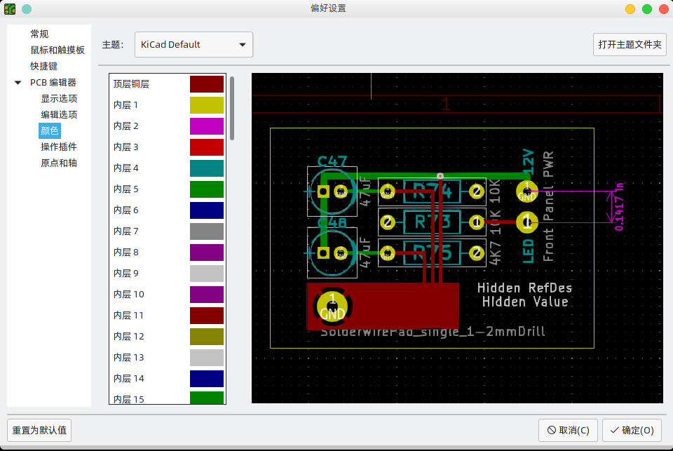
KiCad supports switching between different color themes to match your preferences. Kicad 10.0 comes with two built-in color themes: "KiCad Default" is a new theme designed to have good contrast and balance for most cases and is the default for new installations. "KiCad Classic" is the default theme from KiCad 5.1 and earlier versions. Neither of these built-in themes can be modified, but you can create new themes to customize the look of KiCad as well as install themes made by other users.
颜色主题存储在位于 KiCad 配置目录的 Colors 子目录中的 JSON 文件中。“打开主题文件夹” 按钮将在您的系统文件管理器中打开此位置,使您可以轻松地管理已安装的主题。要安装新主题,请将其放在此文件夹中,然后重新启动 KiCad。如果文件是有效的颜色主题文件,则从颜色主题下拉列表中可以看到新主题。
要创建一个新的颜色主题,从颜色主题的下拉列表中选择 “新主题…”。 为你的主题输入一个名称,然后开始编辑颜色。 新主题中的颜色将从你创建新主题之前选择的任何主题中复制。
要更改颜色,请双击或中键单击列表中的色样。“重置为默认值” 按钮会将该颜色重置为 “KiCad 默认” 颜色主题中的相应条目。
颜色主题会自动保存;当您关闭 "偏好设置" 对话框时,所有更改都会立即反映出来。对话框右侧的窗口显示所选主题外观的预览。
操作插件
KiCad PCB 编辑器支持用 Python 编写的插件,对正在编辑的电路板进行操作。 这些插件可以使用内置的 “插件和内容管理器” 来安装(详见 KiCad 章节),或者将插件文件放在用户的插件目录中。 详见下面的脚本部分。
Each plugin that is detected will be shown in a row on this preferences page. Plugins may show a button on the top toolbar of the PCB editor. If the Show button control is unchecked for a plugin, it may still be accessed from the Tools → External Plugins menu.
列表底部的箭头控制允许改变插件在工具栏和菜单中的显示顺序。 文件夹按钮将启动一个文件资源管理器到插件文件夹,以使安装新的插件更容易。 刷新按钮将扫描插件文件夹中的任何新的或删除的插件,并更新列表。
原点和轴
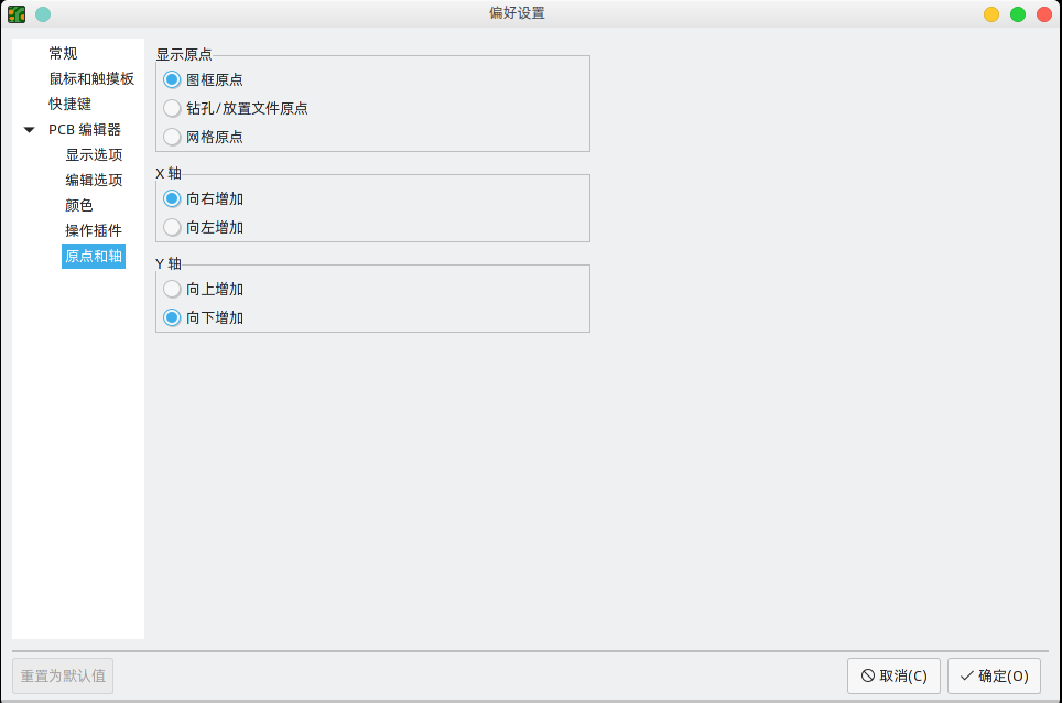
Display origin: Determines which coordinate origin is used for coordinate display in the editing canvas. The page origin is fixed at the corner of the page. The drill/place file origin and the grid origin can be moved by the user.
X axis: Controls whether X-coordinates increase to the right or to the left.
Y axis: Controls whether Y-coordinates increase upwards or downwards.
文本变量
KiCad supports text variables, which allow you to reference predefined variables by name in many kinds of text. KiCad will substitute the variable name with the text string assigned to the variable. Text variables can be used in schematic and PCB graphic text, symbol and footprint text, symbol and footprint fields, drawing sheet fields, custom DRC rules, and other text contexts. This substitution happens anywhere the variable name is used inside the variable replacement syntax of ${VARIABLENAME}.
For example, you could create a variable named VERSION and set the text substitution to 1.0. Now, in any text object on the PCB, you can enter ${VERSION} and KiCad will display this as 1.0. If you change the value to 2.0, every text object that includes ${VERSION} will be updated automatically. You can also mix regular text and variables: a text object with the text Version: ${VERSION} will be displayed as Version: 1.0.
You can define text variables in the schematic or board setup dialogs. These are referred to as project text variables because they are defined for the whole project, so a project text variable defined in the Schematic Editor can also be used in the Board Editor, and vice versa.
The PCB Editor also has a number of built-in system text variables, which are listed in the table below. System text variables may be available in some contexts and not others. There is an equivalent list of variables for the Schematic Editor.
| Variable name | Description |
|---|---|
|
Column (letter) and row (zero-indexed number) address of current table cell. This variable is only available in table cells. |
|
Contents of the table cell indexed by |
|
Column number (zero-indexed) of current table cell. This variable is only available in table cells. |
|
Contents of drawing sheet’s |
|
Contents of drawing sheet’s |
|
Today’s date, in ISO format. |
|
The current time, in |
|
The current time, in your current locale’s time format. |
|
Filename of the board, with a file extension. |
|
Full file path of the board, with a file extension. |
|
Contents of drawing sheet’s |
|
Current version of KiCad. This variable is only available in drawing sheet fields. |
|
Layer of the object. In footprint fields and text objects in footprints, this is
the layer of the field/text object, not the layer of the parent footprint. In
drawing sheet fields, this resolves to the plotted layer, for example |
|
Current sheet’s paper size. This variable is only available in drawing sheet fields. |
|
Project name, without a file extension. |
|
Contents of drawing sheet’s |
|
Row number (zero-indexed) of current table cell. This variable is only available in table cells. |
|
Contents of drawing sheet’s |
|
Name of the currently active design variant. Resolves to an empty string when the default variant is active. |
|
Description of the currently active design variant. Resolves to an empty string when the default variant is active or the active variant has no description. |
|
Full hash of the project’s current Git commit. If the project is not part of a Git repository, resolves to "no hash". |
|
Short (8 character) hash of the project’s current Git commit. If the project is not part of a Git repository, resolves to "no hash". |
|
Contents of project text variable
|
|
Contents of footprint field Both built-in footprint fields and user-defined fields from the
corresponding symbol are available. Built-in footprint fields use all
uppercase letters: for example, to access a footprint’s value, use
Built-in footprint fields are
|
|
Contents of field Both built-in footprint fields and user-defined fields from the
corresponding symbol are available. Built-in footprint fields use all
uppercase letters: for example, to access the value of Built-in footprint fields are
Note: If the footprint referenced by |
|
Generates a DRC error named For example, a text item containing |
|
Generates a DRC warning named |
Text expressions
KiCad has a system for evaluating text expressions, which allows you to manipulate text, evaluate mathematical expressions in strings, and dynamically create strings based on other information. Text expressions can be used in schematic and PCB graphic text, symbol and footprint text, symbol and footprint fields, drawing sheet fields, and other text contexts.
Text expressions are evaluated when the @{expression} syntax is used. Everything inside the braces is evaluated, and the entire expression, including the surrounding @{}, is replaced by the evaluated results. If the expression cannot be evaluated, the expression is not replaced and the original text is retained.
As a basic example, a text object containing 1 plus 1 is @{1 + 1} will read 1 plus 1 is 2.
Many expression functions are provided to perform more complex operations. The available expression functions are detailed in the tables below. For example, the absolute value of a number can be calculated using the abs function: @{abs(-1)} evaluates to 1.
A single text item can contain multiple text evaluations, and evaluations can be nested. You can also combine text evaluations with text variables. For example, @{max(1, 2, 3)}, @{max(4, 5, 6)} evaluates to 3, 6. If the text variable var is defined as -10, a text item containing @{max(abs(${var}), 5)} evaluates to 10.
Numbers can be written in scientific notation, so @{2e3 + 1} evaluates to 2001.
Text expressions support units. Results are always printed in SI units, and the unit is not printed. For example, @{1mm + 1in} evaluates to 26.4.
In addition to numbers, some expression functions operate on strings. A string is text that is enclosed with single or double quotes, like 'string 1' or "string 2". An example of an expression function that operates on strings is upper, which converts a string to uppercase. @{upper("string")} evaluates to STRING.
You can concatenate multiple strings or strings and numbers using the concat expression function or using the + operator: @{concat("hello ", "world")} and @{"hello " + "world"} both evaluate to hello world. @{concat("revision ", 1)} and @{"revision " + 1} both evaluate to revision 1.
Mathematical and logical expressions
The following arithmetic operations are available for operations between two numbers. The operators are all infix operators and obey order of operations. Parentheses can be used for grouping. For example, @{3 + 4 * 3} evaluates to 15, and @{(3 + 4) * 3} evaluates to 21.
| Arithmetic operator | Description | Example |
|---|---|---|
|
Addition Note: |
|
|
Subtraction |
|
|
Multiplication |
|
|
Division (the expression is not evaluated if the divisor is |
|
|
Modulo (the expression is not evaluated if the divisor is |
|
|
Exponentiation (right-associative) |
|
The following expression functions are available for performing mathematical functions. For example, @{abs(-1)} evaluates to 1.
| Expression function | Description | Example |
|---|---|---|
|
Evaluates to the absolute value of |
|
|
Evaluates to the square root of |
|
|
Evaluates to |
|
|
Evaluates to the greatest integer less than or equal to |
|
|
Evaluates to the smallest integer greater than or equal to |
|
|
Evaluates to |
|
|
Evaluates to the minimum of the given comma-separated values. |
|
|
Evaluates to the maximum of the given comma-separated values. |
|
|
Evaluates to the sum of the given comma-separated values. |
|
|
Evaluates to the average of the given comma-separated values. |
|
|
Evaluates to a random number between |
|
|
Evaluates to the equivalent resistance of the two parallel resistances |
|
|
Converts the power ratio |
|
|
Converts the voltage or current ratio |
|
|
Converts the quantity |
|
|
Converts the quantity |
|
|
Evaluates to the closest E-series standard value to |
|
|
Evaluates to the closest E-series standard value greater than |
|
|
Evaluates to the closest E-series standard value less than |
|
Boolean expressions
The following boolean operations are available. These operations evaluate to 1 if the expression is true or 0 if it is false.
| Arithmetic operator | Description | Example |
|---|---|---|
|
Less than |
|
|
Less than or equal to |
|
|
Greater than |
|
|
Greater than or equal to |
|
|
Equal to |
|
|
Not equal to |
|
The following expression functions are available for operating on the result of a boolean or mathematical expression.
| Expression function | Description | Example |
|---|---|---|
|
Evaluates to |
|
String manipulation
The following expression functions are available for manipulating strings.
Strings are text that is surrounded by single or double quotes.
For example, "this is a string" and 'this is also a string'.
|
| Expression function | Description | Example |
|---|---|---|
|
Evaluates to |
|
|
Evaluates to |
|
|
Evaluates to the given comma-separated strings or numbers concatenated together. Note: strings and numbers can also be concatenated using the |
|
|
Evaluates to the portion of |
|
|
Evaluates to the portion of |
|
|
Evaluates to the portion of |
|
|
Evaluates to the portion of |
|
|
Evaluates to |
|
|
Formats Note: |
|
|
Formats Note: |
|
|
Formats |
|
Date and time formatting
The following expression functions are available for manipulating dates and times.
| Expression function | Description | Example |
|---|---|---|
|
Evaluates to the current date, represented as the number of days since the Unix epoch (00:00:00 UTC on 1970-01-01). Note: this value can be formatted in various ways using the |
|
|
Evaluates to the current timestamp, represented as the number of seconds since the Unix epoch (00:00:00 UTC on 1970-01-01). Note: you can add or subtract numbers to this value to get timestamps relative to the current timestamp. |
|
|
Formats |
|
|
Evaluates to the day of the week of the date represented by |
|
|
Formats |
|
Version control expressions
The following expression functions are available for extracting version control system information about the project. If the project is not under version control, each expression function evaluates to <unknown>.
Git is the only supported version control system for these expression functions.
| Expression function | Description |
|---|---|
|
Evaluates to the current HEAD commit identifier, truncated to |
|
Evaluates to the current branch name. |
|
Evaluates to the current HEAD commit’s author’s name. |
|
Evaluates to the current HEAD commit’s author’s email address. |
|
Evaluates to the current HEAD commit’s committer’s name. |
|
Evaluates to the current HEAD commit’s committer’s email address. |
|
Evaluates to the current HEAD commit’s commit date.
Valid values for |
|
Evaluates to the name of the matching tag closest to the HEAD commit.
|
|
Evaluates to the number of commits between HEAD and the matching tag closest to the HEAD commit.
|
|
Evaluates to |
|
Evaluates to the given |
|
Evaluates to the commit identifier of the last commit that modified the specified |
|
Evaluates to the name of the author of the last commit that modified the specified |
|
Evaluates to the email address of the author of the last commit that modified the specified |
|
Evaluates to the name of the committer of the last commit that modified the specified |
|
Evaluates to the email address of the committer of the last commit that modified the specified |
|
Evaluates to the commit date of the last commit that modified the specified |
Graphical design rule editor
The graphical design rule editor lets you create and manage design rules using form controls instead of raw rule syntax. Rules created in the graphical editor are stored in the same .kicad_dru file as rules written in the custom design rules text editor, and the two editors can be used interchangeably on the same file.
The graphical editor covers clearances, track widths, via styles, footprint placement rules, and several high-speed design constraints. For rules not covered by the graphical editor, use the custom design rules text editor instead.
To open the graphical design rule editor, select Design Rule Editor from the Tools menu.
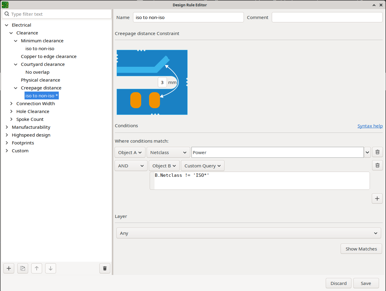
The dialog is divided into two panes. The left pane contains the rule tree, which organizes constraint types by category. The right pane shows the rule editor for the selected item.
Rule tree
The rule tree on the left lists all available constraint types grouped into five categories. Constraint type nodes are shown in bold; user-created rules appear as children beneath them.
-
Electrical: spacing and connection requirements enforced electrically
-
Manufacturability: physical fabrication limits for holes, vias, text, and surface finish
-
Highspeed design: differential pair, skew, and length matching constraints
-
Footprints: placement rules governing layer, orientation, and via proximity
-
Custom: raw-syntax rules for constraint types not covered by the other categories
To create a new rule, select a constraint type node and click the ![]() button in the toolbar at the bottom of the tree, or right-click the node and choose New Rule.
button in the toolbar at the bottom of the tree, or right-click the node and choose New Rule.
To duplicate an existing rule, click the copy button in the toolbar or right-click the rule and choose Copy Rule.
To delete a rule, select it and click the delete button in the toolbar, or right-click and choose Delete Rule.
Rules are evaluated in the same order as the underlying .kicad_dru file. See Custom design rules for details on rule evaluation order.
Rule editor panel
When a rule is selected in the tree, the editor panel on the right shows its settings.
Rule name is a unique identifier for the rule. The name appears in DRC violation reports,
so choose something descriptive such as HV clearance or PWR track width.
Comment is an optional note visible in the rule editor and preserved in the generated rule text.
Constraint values
A visual diagram shows the constraint parameters for the selected constraint type, with editable input fields placed on the diagram at the physically measured location. The diagram varies by constraint type; see the Constraint reference below.
Conditions
The Conditions section determines which board objects the rule applies to. With no conditions set, the rule applies to all objects of the relevant type.
Each condition row filters one object involved in the check. For single-object constraints, each row filters Object A. For two-object constraints such as clearance, each row has an Object A / Object B selector to choose which object is filtered.
The condition type dropdown in each row offers five modes:
-
Any: matches all objects; use this to apply the rule without filtering by net or area
-
Net: matches objects on a specific net (selected from a searchable list)
-
Netclass: matches objects belonging to a net class (selected from a searchable list)
-
Within Area: matches objects inside a named rule area on the board
-
Custom Query: a free-form expression using the custom rule syntax
Multiple conditions can be combined using the ![]() button at the bottom of the conditions section. The boolean operator between each pair of rows is set with the dropdown at the left of each subsequent row and can be AND, OR, AND NOT, or OR NOT. Conditions are evaluated left-to-right without implicit grouping.
button at the bottom of the conditions section. The boolean operator between each pair of rows is set with the dropdown at the left of each subsequent row and can be AND, OR, AND NOT, or OR NOT. Conditions are evaluated left-to-right without implicit grouping.
To remove a condition row, click the delete button at the right end of the row.
Click Syntax help (top right of the conditions section) for a quick reference to the custom rule expression language.
Layer
The Layer selector at the bottom of the panel limits which board layers the rule applies to. The available choices depend on the constraint type:
-
Any: applies on all relevant layers (default)
-
A specific layer name: applies only on that layer
-
Outer: applies on
F.CuandB.Cuonly -
Inner: applies on internal copper layers only
Show Matches highlights all board objects that currently satisfy the rule condition. Use this before saving a rule to confirm the condition selects the right objects.
After setting all values, click Save to store the rule, or Discard to abandon changes.
Constraint reference
Electrical
Minimum clearance |
Minimum copper-to-copper gap. |
Copper to edge clearance |
Minimum distance from any copper object to the board outline. |
Courtyard clearance |
Minimum spacing between footprint courtyard boundaries. |
Physical clearance |
Minimum distance between physical objects, measured to the edge of holes. |
Creepage distance |
Minimum surface creepage distance between conductors at different potentials. |
Minimum connection width |
Minimum width for copper connections, including tracks and filled zone connections. |
Copper to hole clearance |
Minimum distance from any copper shape to the edge of any drilled hole. |
Minimum thermal relief spoke count |
Minimum number of thermal relief spokes connecting a pad to a zone fill. |
Manufacturability
Minimum annular width |
Minimum annular ring width around through-hole pads and vias. |
Minimum drill size |
Minimum allowable drill diameter. |
Hole to hole distance |
Minimum edge-to-edge spacing between any two holes. |
Via style |
Minimum and maximum via pad diameter and drill size. An optional Via type filter restricts the rule to a specific via type: Any, Through, Micro, Blind, or Buried. |
Minimum text height and thickness |
Minimum character height and stroke thickness for text on any layer. |
Silk to silk clearance |
Minimum spacing between silkscreen objects. |
Silk to soldermask clearance |
Minimum distance from silkscreen objects to the edge of soldermask openings. |
Minimum soldermask silver |
Minimum soldermask sliver width between adjacent pad openings. |
Soldermask expansion |
Minimum and maximum soldermask opening expansion relative to the pad. |
Solderpaste expansion |
Minimum and maximum solderpaste aperture size relative to the pad. |
Highspeed design
Routing width |
Minimum, optimal (preferred), and maximum track width. The preferred width is used by the router as the default when placing new tracks. |
Maximum via count |
Maximum number of vias permitted in a net. |
Routing diff pair |
Maximum skew tolerance between the two signals in a differential pair. |
Matched length diff pair |
Maximum length mismatch between the two signals in a differential pair, plus minimum and maximum gap between the pair conductors. |
Absolute length |
Minimum and maximum total routed length for a net. |
Footprints
Permitted layers |
Checkboxes to allow placement on the top layer, the bottom layer, or both. Footprints placed on a layer that is not checked generate a DRC error. |
Allowed orientation |
Checkboxes for 0°, 90°, 180°, 270°, and All. Footprints placed at a rotation that is not checked generate a DRC error. |
Vias under SMD |
Whether vias are permitted directly beneath SMD pads. |
Custom
Select Custom rule to enter a rule using the full custom design rule syntax. The text editor supports syntax highlighting and autocomplete. Click Check syntax to validate the rule before saving. For a complete syntax reference, see Custom design rules.
例子
Minimum clearance for a high-voltage net class
This rule enforces a 1.5 mm minimum clearance between any object in the HV net class and any other object.
-
Select Tools → Design Rule Editor.
-
In the rule tree, expand Electrical → Clearance and select Minimum clearance.
-
Click the
 button or right-click and choose New Rule. A new rule named
 Minimum clearance 1appears in the tree. -
In the Rule name field, change the name to
HV clearance. -
In the Conditions section, set the Condition type to Netclass and select
HV. Leave the Object selector set toA. -
Set the clearance value to
1.5. -
Click Save.
Run the DRC to verify that objects in the HV net class are flagged when their clearance to any other copper object falls below 1.5 mm.
Preferred track width for power nets
This rule sets a preferred routing width of 0.5 mm and a minimum of 0.25 mm for all nets in the PWR net class.
-
Select Tools → Design Rule Editor.
-
Expand Highspeed design → Diff Pair (width, gap, uncoupled length) and select Routing width.
-
Click
to create a new rule and name it PWR track width. -
Set the Condition type to Netclass and select
PWR. -
In the constraint diagram, set Min to
0.25, Opt to0.5, and Max to1.0. -
Click Save.
The interactive router will now default to 0.5 mm when routing nets in the PWR net class and will enforce the 0.25 mm minimum width.
Restricting a footprint to the top side only
This rule generates a DRC error whenever any U-reference footprint is placed on the bottom of the board.
-
Select Tools → Design Rule Editor.
-
Expand Footprints → Allowed Layers and select Permitted layers.
-
Click
to create a new rule and name it ICs top only. -
Set the Condition type to Custom Query and enter:
A.Reference == 'U*'
-
Check Allow top layer and uncheck Allow bottom layer.
-
Click Show Matches to confirm the condition selects the correct footprints.
-
Click Save.
The Permitted layers and Allowed orientation constraints use the assertion
constraint type internally. Violations appear as Assertion violation errors in the
DRC report. The rule name identifies which assertion was violated.
|
Custom design rules
KiCad’s custom design rule system allows creating design rules that are more specific than the generic rules available in the Constraints page of the Board Setup dialog. Custom design rules have many applications, but in general they are used to apply certain rules to a portion of the board, such as a specific net or net class, a specific area, or a specific footprint.
自定义设计规则存储在一个扩展名为 kicad_dra 的单独文件中。当您开始向项目添加自定义规则时,会自动创建此文件。如果您在项目中使用自定义规则,请在备份或提交到版本控制系统时,确保将 kicad_dra 文件与 kicad_pcb 和 kicad_pro 文件一起保存。
kicad_dra 文件由 KiCad 自动管理,不应使用外部文本编辑器进行编辑。
始终使用电路板设置对话框的自定义规则页面编辑自定义设计规则。
|
自定义规则编辑器
自定义规则编辑器位于电路板设置对话框中,它提供了一个用于输入自定义规则的文本编辑器,一个语法检查器将测试你的自定义规则并指出任何错误,还有一个语法帮助对话框,其中包含了对自定义规则语言的快速参考和一些规则示例。
The custom rules editor also provides context-sensitive autocomplete to suggest valid keywords and properties. The autocomplete suggestion menu appears automatically, but it can also be opened manually by pressing Ctrl+Space.
在编辑自定义规则后,最好使用 检查规则语法 按钮,确保没有语法错误。 自定义规则中的任何错误将阻止设计规则检查器的运行。
自定义规则语法
The custom design rule language is based on s-expressions and allows you to create design constraints that are not possible with the built-in constraints. Each design rule generally contains a condition defining what objects to match and a constraint defining the rule to be applied to the matched objects.
The language uses parentheses (( and )) to define clauses of related keywords and values. Parentheses must always be matched: for every ( there must be a matching ). Inside a clause, keywords and values are separated by whitespace (spaces, tabs, and newlines). By convention, a single space is used, but any number of whitespace characters between keywords and values is acceptable. In places where text strings are valid, strings without any whitespace may be quoted with " or ', or unquoted. Strings that contain whitespace must always be quoted. Newlines cannot be used within a quoted string. Where nested quotes are required, a single level of nesting is possible by using " for the outer quote character and ' for the inner (or vice versa). Newlines between clauses are not required, but are typically used in examples for clarity.
In the syntax descriptions below, items in <angle brackets> represent keywords or values that must be present and items in [square brackets] represent keywords or values that are optional or only sometimes required.
The Custom Rules file must start with a version header defining the version of the rules language. As of KiCad 10.0, the version is 1. The syntax of the version header is (version <number>). So in KiCad 10.0 the header should read:
(version 1)
在版本头之后,您可以输入任何数量的规则。 规则的评估顺序是相反的,也就是说,文件中的最后一条规则首先被检查。 一旦为一个给定的被测对象找到一个匹配的规则,将不再检查其他规则。在实践中,这意味着更具体的规则应该在文件的后面,以便它们在更通用的规则之前被评估。
例如,如果您创建一条规则来限制 HV 网络的布线与任何其他网络的布线之间的最小间距,然后又创建第二条规则来限制特定规则区域内所有对象的最小间距,请确保第一条规则在自定义规则文件中的出现时间比第二条规则晚,否则,如果 HV 网络中的布线落在规则区域内,可能会有错误的间距。
Each rule must have a name and one or more constraint clauses. The name can be any string and is used to refer to the rule in DRC reports. The constraint defines the behavior of the rule. Rules may also have a condition clause that determines which objects should have the rule applied, an optional layer clause which specifies which board layers the rule applies to, and an optional severity clause which specifies the severity of the resulting DRC violation.
(rule <name>
    [(severity <severity>)]
    [(layer <layer_name>)]
    [(condition <expression>)]
    (constraint <constraint_type> [constraint_arguments]))
The custom rules file may also include comments to describe rules. Comments are denoted by any line that begins with the # character (not including whitespace). You can press Ctrl+/ to comment or uncomment lines automatically.
# Clearance for 400V nets to anything else
(rule HV
    (condition "A.hasNetclass('HV')")
    (constraint clearance (min 1.5mm)))
Custom rules can reference text variables. These are not technically part of the custom rules syntax, but are resolved in a preprocessing step before evaluating the rules file. Because text variables are resolved as a simple text replacement, they can be used anywhere in the DRC rules, as long as all rules are syntactically valid after the variables have been resolved.
Text variables could be used, for example, to define a project-wide value that is used in one or more constraints, like (constraint clearance (min ${hv_clearance})), where ${hv_clearance} is a text variable defined in the project as ${3 mm}.
Not all text variables can be resolved in custom rules. Some text variables resolve to different values depending on the object they are a part of, such as ${LAYER} or ${<fieldname>}. Because text variables in custom rules are resolved before evaluating any rules or applying rules to specific objects in the board, such text variables cannot be resolved in custom rules. Any text variables that cannot be resolved will remain in their unresolved state and cause a syntax error when the rules file is evaluated.
图层子句
层 (layer) 子句确定规则将对哪些层起作用。虽然对象层可以在下面介绍的 约束 (constraint) 子句中进行测试,但是使用 层 (layer) 子句效率更高。
The value in the layer clause can be any board layer name, or the shortcut keywords outer to match the front and back copper layers (F.Cu and B.Cu) and inner to match any internal copper layers.
如果省略 层 (layer) 子句,则该规则将适用于所有层。
下面是一些示例:
# Do not allow footprints on back layer (no condition clause means this rule always applies)
(rule "Top side footprints only"
    (layer B.Cu)
    (constraint disallow footprint))

# This rule does the same thing, but is less efficient
(rule "Top side footprints only"
    (condition "A.Layer == 'B.Cu'")
    (constraint disallow footprint))

# Larger clearance on outer layers (inner layer clearance set by board minimum clearance)
(rule "clearance_outer"
    (layer outer)
    (constraint clearance (min 0.25mm)))
Severity Clause
The severity clause sets the DRC violation severity whenever the rule is violated.
Possible values are error, warning, ignore, and exclusion. Ignored rules are not observed by the interactive router and violations are not shown in the DRC dialog. However, ignored rules are evaluated for matching and therefore can still override earlier rules. Errors, warnings, and excluded rules are all observed by the interactive router, and violations are displayed in the DRC dialog when the appropriate filters are selected.
Setting a rule’s severity to ignore does not disable the rule; only the effects of the rule are disabled. The rule is still evaluated and can still override previous rules.
|
Condition Clauses
The condition clause determines which objects which objects the rule applies to. If a rule has a condition clause, the rule will apply to any objects that match the condition. If a rule does not have any condition clauses, it will apply unconditionally.
规则 条件 是一个包含在文本字符串中的表达式(因此通常用引号包围,以便允许留出空白,使之更清晰)。 该表达式是针对设计规则检查器正在测试的每一对对象进行评估的。 例如,当检查铜对象之间的间隙时,每个网络上的每个铜对象(布线段、焊盘、通孔等)都要与其他网络上的其他铜对象进行检查。 如果存在一个自定义规则,其表达式与两个给定的铜对象相匹配,并且约束条件定义了铜的间隙,那么这个自定义规则可以用来确定这两个对象之间所需的间隙。
被测对象在表达式语言中称为 A 和 B。这两个对象的顺序并不重要,因为设计规则检查器将测试这两种可能的顺序。例如,您可以编写一条规则,假设 A 为布线,B 为过孔。 有一些表达式函数可以同时测试这两个对象;这些表达式函数使用 AB 作为对象名。
The expression in a condition must resolve to a boolean value (true or false). If the expression resolves to true, the rule is applied to the given objects.
每个被测对象都有可以比较的 属性,以及可以执行特定测试的 函数。属性和函数的使用语法分别为 <object>.<property> 和 <object>.<function>([arguments])。译者注: <对象>.<属性> 和 <对象>.<函数>([参数])。
当你在文本编辑器中输入 <对象>.(A.、B. 或 AB.)时,将打开一个自动完成的列表,其中包含所有可以使用的对象属性。
|
The object properties and functions are compared using boolean and relational operators to result in a boolean expression. The following operators are supported:
|
Equal to |
|
Not equal to |
|
Greater than, greater than or equal to |
|
Less than, less than or equal to |
|
And |
|
Or |
|
Not (unary) |
For example, A.NetName == 'VDD' will apply to any objects that are part of the "VDD" net and A.NetName != B.NetName will apply to any objects that have different net names. Parentheses can be used to clarify the order of operations in complex expressions but they are not required. All the boolean operators have the same precedence and are evaluated in order from left to right.
To test a boolean property, evaluate the property itself, without comparing it to a boolean literal like true or false (which don’t exist in the DRC rules language). For example, to test if a footprint’s boolean Do_not_populate property is set, the boolean expression A.Do_not_populate by itself is sufficient. It will resolve to a true value if the footprint’s DNP attribute is set, and a false value otherwise. To check if a boolean is false, use the ! operator (unary not): !A.Do_not_populate will resolve to a true value if the DNP attribute is unset, and a false value otherwise.
有些属性表示物理测量,比如尺寸、角度、长度、位置等等。 在这些属性上,单位后缀 可以在自定义规则语言中使用,以指定使用什么单位。 如果没有使用单位后缀,属性的内部表示将被使用(距离为纳米,大多数角度为度)。 支持以下后缀:
|
Millimeters |
|
Thousandths of an inch (mils) |
|
Inches |
|
Degrees |
|
Radians |
| 自定义设计规则中使用的单位独立于 PCB 编辑器中的显示单位。 |
Numeric conditions can use simple math expressions, for example (condition "A.Hole_Size_X == 1.0mm + 0.1mm").
Some properties are nullable, i.e. they can have a value, including zero, or no value at all (null). An example is a pad’s Soldermask_Margin_Override property, which can be set to a non-zero margin, a margin of zero, or no override (inherit from parent footprint). To check if a nullable property is null, compare against the token null. For example, (condition "A.Soldermask_Margin_Override != null") matches pads that override the soldermask margin from their parent footprint.
Constraint Clauses
The constraint clause of the rule defines the behavior of the rule on the objects that are matched by the condition. Each constraint clause has a constraint type and one or more arguments that set the behavior of the constraint. A single rule may have multiple constraint clauses, in order to set multiple constraints (for example, clearance and track_width) for objects that match the same rule conditions.
许多约束条件的参数指定了一个物理测量或数量。 这些约束条件支持最小值、最优值和最大值说明(缩写为 "min/opt/max")。 最小 和 最大 值用于设计规则检查:如果实际值小于约束条件中的最小值或大于最大值,将产生一个 DRC 错误。 最优 值仅用于某些约束,并通知 KiCad 默认使用的 "最优" 值。 例如,最优的 diff_pair_gap 是由布线器在放置新的差分对时使用的。 如果后来修改了差分对,使得差分对之间的间隙与最佳值不同,只要间隙在最小值和最大值之间(如果这些值被指定),就不会产生错误。 在所有接受最小/最大/最优值的情况下,可以指定全部的最小值、最优值和最大值。
最小/最优/最大值被指定为 (min<value>), (opt<value>), 和 (max<value>)。例如,布线宽度约束可以写成 (constraint track_width (min 0.5mm) (opt 0.5mm) (max 1.0mm)),如果只约束最小宽度,可以简单写成 (constraint track_width (min 0.5mm)) 。
Numeric constraint values can use simple math expressions, for example (constraint clearance (min 0.5mm + 0.1mm)).
| Constraint type | Argument type | Description |
|---|---|---|
|
min/max |
Checks the width of annular rings on vias and pads. |
|
boolean expression |
Checks that the boolean expression is true. If the expression is false, a DRC error will be created. The expression can use any of the properties listed in the Object Properties section. |
|
Checks for solder mask bridges between copper items. This constraint does not take a min/opt/max value. In combination with a severity clause, this constraint can be used to allow or disallow solder mask bridging in various conditions. |
|
|
min |
Specifies the electrical clearance between copper objects of different nets. (See
To allow copper objects to overlap (collide), create a |
|
min |
Checks the width of connections between pads and zones. An error will be generated for each pad
connection that is narrower than the |
|
min |
Checks the clearance between footprint courtyards and generates an error if any two courtyards
are closer than the To allow courtyard objects to overlap (collide), create a |
|
min |
Specifies the creepage between copper objects of different nets. |
|
min/opt/max |
Checks the gap between parallel tracks in a differential pair. The |
|
max |
Checks the distance that a differential pair track is routed uncoupled from the other polarity
track in the pair (for example, where the pair fans out from a component, or becomes uncoupled
to pass around another object such as a via). An error will be generated for each differential
pair with an uncoupled distance that is greater than the |
|
|
Specify one or more object types to disallow, separated by spaces. For example,
|
|
min |
Checks the clearance between objects and the board edge. This can also be thought of as the "milling tolerance" as the board edge will include all
graphical items on the To allow objects to overlap (collide) with the board edge, create an |
|
min |
Checks the clearance between a drilled hole in a pad or via and copper objects on a different net. The clearance is measured from the diameter of the hole, not its center. |
|
min/opt/max |
Checks the size (diameter) of a drilled hole in a pad or via. For oval holes, the smaller
(minor) diameter will be tested against the |
|
min |
Checks the clearance between mechanically-drilled holes in pads and vias. The clearance is measured between the diameters of the holes, not between their centers. This constraint is solely for the protection of drill bits. The clearance between laser-drilled (microvias) and other non-mechanically-drilled holes is not checked, nor is the clearance between milled (oval-shaped) and other non-mechanically-drilled holes. |
|
min/opt/max |
Checks the total routed length for the nets that match the rule condition and generates an
error for each net that is below the |
|
|
Checks the total number of connections (spokes) to a pad. An error will be raised for each pad that has fewer than the specified number of spokes. |
|
min |
Checks the clearance between two objects, regardless of their nets. This includes objects
with the same net and objects on non-copper layers. Only objects on physical layers and
courtyard layers are checked: this means copper, adhesive, paste, silkscreen, mask,
courtyard, and edge cut layers. Physical clearance is only checked between objects on the
same layer, except for objects on While this can perform more general-purpose checks than |
|
min |
Checks the clearance between a drilled hole in a pad or via and another object, regardless of net. The clearance is measured from the diameter of the hole, not its center. This can also be thought of as the "drilling tolerance" as it only includes round holes
(see |
|
min |
Checks the clearance between objects on silkscreen layers and other objects. To allow silkscreen objects to overlap (collide) with other objects, create a |
|
min/opt/max/within_diff_pairs |
Checks the total skew for the nets that match the rule condition, that is, the difference
between the length of each net and the longest net that is matched
by the rule. If the difference between the longest net and the length of any one net is above
the constraint |
|
opt |
Specifies the solder mask expansion for pads, shapes and tracks. |
|
opt |
Specifies the absolute solder paste clearance for pads. Usually negative to inset the paste. The final solder paste clearance will be the absolute clearance plus the relative clearance. |
|
opt |
Specifies the relative solder paste clearance for pads. Usually negative to inset the paste. The final solder paste clearance will be the absolute clearance plus the relative clearance. |
|
min/max |
Checks the height of text, including text boxes. An error will be generated for each text item
that has a height below the |
|
min/max |
Checks the thickness of text, including text boxes. An error will be generated for each text
item that has a thickness below the |
|
min |
Specifies the width of the gap between a pad and a zone with a thermal-relief connection. |
|
opt |
Specifies the width of the spokes connecting a pad to a zone with a thermal-relief connection. |
|
min/max |
Checks the angle between two connected track segments. An error will be generated for each connected pair with an angle below the min value (if specified) or above the max value (if specified). |
|
min/max |
Checks the length of track and arc segments. An error will be generated for each segment that has a length below the min value (if specified) or above the max value (if specified). |
|
min/opt/max |
Checks the width of track and arc segments. An error will be generated for each segment that
has a width below the |
|
min/max |
Counts the number of vias on every net matched by the rule condition. An error will be generated
for each net that has fewer vias than the |
|
Checks for vias that are unconnected or connected on only one layer. This constraint does not take
a min/opt/max value. In combination with a |
|
|
min/opt/max |
Checks the diameter of vias. An error will be generated for each via that has a diameter below
the |
|
|
Specifies the connection to be made between a zone and a pad. |
对象属性和函数参考
可以在自定义规则表达式中测试以下属性:
共有属性
这些属性适用于所有 PCB 对象。
| Property | Data type | Description |
|---|---|---|
|
string |
The board layer on which the object exists. For objects that exist on more than one layer,
this property will return the first layer (for example, |
|
boolean |
True if the object is locked. |
|
string |
Returns the unique identifier of the parent object of this object. |
|
dimension |
The position of the object’s origin in the X-axis. Note that the origin of an object is not always the same as the center of the object’s bounding box. For example, the origin of a footprint is the location of the (0, 0) coordinate of that footprint in the footprint editor, but the footprint may have been designed such that this location is not in the center of the courtyard shape. |
|
dimension |
The position of the object’s origin in the Y-axis. Note that KiCad always uses Y-coordinates that increase from the top to bottom of the screen internally, even if you have configured your settings to show the Y-coordinates increasing from bottom to top. |
|
string |
One of "Bitmap", "Dimension", "Footprint", "Graphic", "Group", "Leader", "Pad", "Target", "Text", "Text Box", "Track", "Via", or "Zone". |
连接的对象属性
这些属性适用于可以分配网络的铜对象(焊盘、过孔、敷铜、布线)。
| Property | Data type | Description |
|---|---|---|
|
integer |
The net code of the copper object. Note that net codes should not be relied upon to remain
constant: if you need to refer to a specific net in a rule, use |
|
string |
The list of all net classes for the copper object. This is a priority ordered, comma delimited list where a net has multiple net classes assigned. Note that this list may include the In an expression, an object’s
The following expressions are false, however:
You can also check if a copper object is a member of a particular net class,
regardless of any other net classes it may be a part of, using
|
|
string |
The name of the net for the copper object. Note that |
|
boolean |
True if curved edges are enabled for teardrops connected to the object. |
|
boolean |
True if teardrops are enabled for the object. |
|
boolean |
True if the "Prefer zone connections" property is set for the object. |
|
boolean |
True if the "Allow teardrops to span two tracks" property is set for the object. |
|
double |
Best ratio of teardrop length to object size for teardrops connected to the object. |
|
double |
Best ratio of teardrop width to object size for teardrops connected to the object. |
|
dimension |
Maximum length dimension for teardrops connected to the object. |
|
dimension |
Maximum width dimension for teardrops connected to the object. |
|
double |
Maximum allowable ratio of object size to track width for teardrops connected to the object. |
封装属性
These properties apply to footprints. They also apply to footprint children, such as pads and footprint graphics: for example, a footprint pad is considered to have the same Reference as its parent footprint.
| Property | Data type | Description |
|---|---|---|
|
dimension |
The copper clearance override set for the footprint. |
|
string |
The name of the component class set for the footprint. This is an alphabetically ordered, comma delimited list where a footprint has multiple component classes assigned. In an expression, a footprint’s
The following expressions are false, however:
Note that while You can also check if an object is part of a footprint with a specific component class using
the |
|
boolean |
True if the footprint’s "Do not populate" attribute is set. |
|
boolean |
True if the footprint’s "Exclude from position files" attribute is set. |
|
boolean |
True if the footprint’s "Exclude from bill of materials" attribute is set. |
|
boolean |
True if the footprint’s "Exempt from courtyard requirement" attribute is set. |
|
string |
The "Keywords" from the library footprint. |
|
string |
The footprint’s description in the footprint library. This is the footprint’s
description property, not the contents of the footprint field named |
|
string |
The link to the library footprint in |
|
boolean |
True if the footprint’s "Not in schematic" attribute is set. |
|
double |
The orientation (rotation) of the footprint in degrees. |
|
string |
The reference designator of the footprint. Note that while |
|
dimension |
The solder paste margin override set for the footprint. |
|
dimension |
The solder paste margin ratio override set for the footprint. |
|
dimension |
The thermal relief gap set for the footprint. |
|
dimension |
The thermal relief connection width set for the footprint. |
|
string |
The contents of the "Value" field of the footprint. Note that while |
|
string |
One of "Inherited", "None", "Thermal reliefs" or "Solid". |
焊盘属性
这些属性适用于封装焊盘。
| Property | Data type | Description |
|---|---|---|
|
dimension |
The copper clearance override set for the pad. |
|
string |
One of "None", "BGA pad", "Fiducial, global to board", "Fiducial, local to footprint", "Test point pad", "Heatsink pad", "Castellated pad". |
|
dimension |
The size of the pad’s drilled hole/slot in the X axis. |
|
dimension |
The size of the pad’s drilled hole/slot in the Y axis. |
|
double |
The orientation (rotation) of the pad in degrees. |
|
string |
The "number" of a pad, which can be a string (for example "A1" in a BGA). |
|
string |
One of "Circle", "Rectangle", "Oval", "Trapezoid", "Rounded rectangle", "Chamfered rectangle", or "Custom". |
|
dimension |
The value of the "pad to die length" property of a pad, which is additional length added to the pad’s net when calculating net length. |
|
string |
One of "Through-hole", "SMD", "Edge connector", or "NPTH, mechanical". |
|
string |
The name of the pad (usually the name of the corresponding pin in the schematic). |
|
string |
The electrical type of the pad (usually taken from the corresponding pin in the schematic). One of "Input", "Output", "Bidirectional", "Tri-state", "Passive", "Free", "Unspecified", "Power input", "Power output", "Open collector", "Open emitter", or "Unconnected". Pins with a no-connection flag on them will have a "+no_connect" suffix added to the pin type string. For example, "passive+no_connect" will match a passive pin with a no-connection flag. To match a pin type whether or not the pin has a no-connection flag, use a wildcard: "passive*" will match passive pins with or without a no-connection flag. |
|
double |
For rounded rectangle pads, the ratio of radius to rectangle size. |
|
dimension |
The size of the pad in the X-axis. |
|
dimension |
The size of the pad in the Y-axis. |
|
dimension |
The solder mask margin override set for the pad. |
|
dimension |
The solder paste margin override set for the pad. |
|
dimension |
The solder paste margin ratio override set for the pad. |
|
dimension |
The thermal relief gap set for the pad. |
|
dimension |
The thermal relief connection angle set for the pad. |
|
dimension |
The thermal relief connection width set for the pad. |
|
string |
One of "Inherited", "None", "Thermal reliefs" or "Solid". |
布线和圆弧属性
这些属性适用于布线和弧形布线。
| Property | Data type | Description |
|---|---|---|
|
dimension |
The x-coordinate of the start point. |
|
dimension |
The y-coordinate of the start point. |
|
dimension |
The x-coordinate of the end point. |
|
dimension |
The y-coordinate of the end point. |
|
dimension |
The width of the track or arc. |
过孔属性
这些属性适用于过孔。
| Property | Data type | Description |
|---|---|---|
|
dimension |
The diameter of the via’s pad. |
|
dimension |
The diameter of the via’s finished hole. |
|
string |
The last layer in the via stackup. |
|
string |
The first layer in the via stackup. |
|
string |
One of "Blind", "Buried", "Micro", or "Through". |
Tuning Pattern Properties
These properties apply to tuning patterns.
| Property | Data type | Description |
|---|---|---|
|
dimension |
The x-coordinate of the end point. |
|
dimension |
The y-coordinate of the end point. |
|
dimension |
The minimum amplitude of the tuning pattern. |
|
dimension |
The maximum amplitude of the tuning pattern. |
|
string |
One of "Single track", "Differential pair", or "Diff pair skew". |
|
string |
One of "Left", "Right", or "Default". |
|
dimension |
The minimum spacing of the tuning pattern.. |
|
integer |
The corner radius percentage of the tuning pattern. |
|
dimension |
The target length for the tuning pattern. |
|
dimension |
The target skew for the tuning pattern. |
|
boolean |
True if the tuning pattern overrides custom DRC rules. |
|
boolean |
True if the tuning pattern is single-sided. |
|
boolean |
True if the tuning pattern uses rounded meanders. |
敷铜和规则区域属性
这些属性适用于铜区和非铜区,以及规则区(以前称为禁止布线区)。
| Property | Data type | Description |
|---|---|---|
|
dimension |
The copper clearance override set for the zone. |
|
dimension |
The distance between hatched lines in the zone. |
|
float |
The minimum allowed hatching hole size, expressed as a fraction of the nominal hatching hole size. |
|
integer |
The angle (in degrees) of the hatched lines in the zone. |
|
dimension |
The width of hatched lines in the zone. |
|
dimension |
The minimum allowed width of filled areas in the zone. |
|
string |
The user-specified name (blank by default). |
|
string |
One of "Inherited", "None", "Thermal reliefs", "Solid", or "Thermal Reliefs for PTH". |
|
integer |
The priority level of the zone. |
|
dimension |
The thermal relief gap set for the zone. |
|
dimension |
The thermal relief connection width set for the zone. |
图形形状属性
这些属性适用于图形线、圆弧、圆、矩形和多边形。
| Property | Data type | Description |
|---|---|---|
|
dimension |
The angle of an arc. |
|
dimension |
The x-coordinate of the end point. |
|
dimension |
The y-coordinate of the end point. |
|
boolean |
True if the shape is filled. |
|
dimension |
Thickness of the strokes of the shape. |
|
string |
One of "Solid", "Dashed", "Dotted", "Dash-Dot", "Dash-Dot-Dot". |
|
string |
One of "Segment", "Rectangle", "Arc", "Circle", "Polygon", or "Bezier". |
|
dimension |
The x-coordinate of the start point. |
|
dimension |
The y-coordinate of the start point. |
文本属性
这些属性适用于文本对象(封装字段、自由文本标签等)。
| Property | Data type | Description |
|---|---|---|
|
boolean |
True if the text is bold. |
|
dimension |
Height of a character in the font. |
|
string |
Horizontal text justification (alignment): one of "Left", "Center", or "Right". |
|
boolean |
True if the text is italic. |
|
boolean |
True if the text has the knockout property set. |
|
boolean |
True if the text is mirrored. |
|
string |
The name of a footprint field. For text objects that are not footprint fields, this is an empty string. |
|
string |
The contents of the text object. |
|
dimension |
Thickness of the stroke of the font. |
|
dimension |
Width of a character in the font. |
|
string |
Vertical text alignment: one of "Top", "Center", or "Bottom". |
|
boolean |
True if the text object is visible (displayed). |
表达式函数
可以对自定义规则表达式中的对象调用以下函数:
| Function | Objects | Description |
|---|---|---|
|
|
Returns true if all of the object is inside the named rule area or zone. Note that
|
|
|
Returns true if the object exists on the given board layer. |
|
|
Returns true if the object exists on the copper path between the given pads. |
|
|
Returns the value of field |
|
|
Returns true if the set of component classes assigned to the object, or the object’s parent footprint, contains the named component class |
|
|
Returns true if the set of net classes assigned to the object exactly matches the named set of net
classes |
|
|
Returns true if the set of net classes assigned to the object contains the named net class |
|
|
Returns true if the object is part of a differential pair and the base name of the pair
matches the given argument |
|
|
Returns true if any part of the object is inside the named rule area or zone. Rule area and zone names can be set in their respective properties dialogs. If the given area is a filled copper zone, the function tests if the given object is inside any of the filled copper regions of the zone, not if the object is inside the zone’s outline. Deprecated; use |
|
|
Returns true if the any part of the object is inside the courtyard of the given footprint. The
first variant checks both the front or back courtyard and returns true if the object is inside
either one; the second and third variants check a courtyard on a specific layer.
The named footprint
Deprecated; use |
|
|
Returns true if any part of the object is inside the named rule area or zone. Rule area and zone names can be set in their respective properties dialogs. If the given area is a filled copper zone, the function tests if the given object is inside any of the filled copper regions of the zone, not if the object is inside the zone’s outline. |
|
|
Returns true if any part of the object is inside the courtyard of the given footprint. The
first variant checks both the front or back courtyard and returns true if the object is inside
either one; the second and third variants check a courtyard on a specific layer.
The named footprint
|
|
|
Returns true if the object is a blind via. |
|
|
Returns true if the object is a buried via. |
|
|
Returns true if the object is a blind via or a buried via. |
|
|
Returns true if the two objects being tested are part of the same differential pair but are
opposite polarities. For example, returns true if |
|
|
Returns true if the object is a microvia. |
|
|
Returns true if the object is a plated hole (in a pad or via). |
|
|
Returns true if the object is a member of the named group Deprecated; use |
|
|
Returns true if the object is a member of a group named |
|
|
Returns true if the object is a member of the given footprint.
The named footprint
|
|
|
Returns true if the object is a member of a schematic sheet named |
|
|
Returns true if the object is a member of a schematic sheet named |
From-To signal path matching
In high-speed PCB design, constraining an entire net is often too coarse. A single net may connect many pads, but only a specific segment of that net — the path between two particular pads — carries the timing-critical signal. For example, a DDR data net may run from a memory controller pad to a DRAM pad, but the same net also fans out to termination resistors or test points. Applying a length constraint to the whole net would include copper that is irrelevant to the high-speed signaling path.
From-To paths solve this problem. A From-To path is a designer-defined signal path between two specific pads on a board. By identifying the copper objects (tracks, vias, and pads) that form the unique electrical path between a source pad and a destination pad, From-To paths allow custom DRC rules to target exactly the portion of a net that matters for signal integrity.
This concept is analogous to Altium Designer’s xSignals feature, where designers define specific signal paths to scope length-matching and other high-speed design rules to individual point-to-point connections rather than entire nets.
How From-To paths work
When a custom DRC rule uses the fromTo() function, KiCad evaluates From-To paths for the board. The process works as follows:
-
Endpoint discovery: KiCad scans every footprint on the board and builds a list of pad endpoints. Each endpoint is identified by a name in the format
RefDes-PadNumber(for example,U1-A5orR3-1). Each pad is also identified by just the parent footprint’s reference designator (for example,U1), allowing rules to match all pads of a footprint. -
Pad matching: The
fromandtoarguments are matched against endpoint names using wildcard comparison. The wildcards*(match any sequence of characters) and?(match a single character) are supported. Matching is case-insensitive. -
Path tracing: For each pair of matching endpoints that share the same net, KiCad traces the copper connectivity to find the path between them. The path includes all tracks, vias, and pads that lie on the electrical route between the two endpoints.
-
Uniqueness check: KiCad determines whether the path between the two pads is unique — that is, whether there is exactly one route between the pads. If there are multiple paths (for example, because of a ground plane or copper pour connecting the pads through more than one route), the path is still found but is marked as non-unique.
If the from pattern matches a pad that has more than one connected pad matching the to
pattern on the same net, the path cannot be unambiguously determined and will not be
created. Make your from and to patterns specific enough to identify exactly one pad at
each end.
|
Pad name format
Pad endpoints used in fromTo() follow a specific naming convention:
| Format | Description |
|---|---|
|
Matches a specific pad on a specific footprint. For example, |
|
Matches all pads on the given footprint. For example, |
Wildcards |
Both |
Using fromTo() in custom DRC rules
The fromTo() function is used in the condition clause of a custom DRC rule. It takes two string arguments: the from pad identifier and the to pad identifier. The function returns true if the object being tested (either A or B) lies on the copper path between the specified pads.
The basic syntax is:
(rule <name>
    (condition "A.fromTo('<from_pad>', '<to_pad>')")
    (constraint <constraint_type> <arguments>))
The fromTo() function is most commonly combined with the following constraint types:
| Constraint | Use with fromTo() |
|---|---|
|
Constrain the total routed length of a specific signal path, rather than the entire net. |
|
Match lengths across a group of signal paths (for example, a DDR data bus) by constraining the skew between paths. |
|
Enforce specific trace widths on high-speed signal paths. |
|
Apply tighter or looser clearance rules to specific signal paths. |
|
Control differential pair spacing on specific segments. |
From-To path examples
Length-constrain a specific signal path
To constrain the routed length of a specific signal path between a memory controller and a DRAM chip, rather than constraining the entire net:
# Constrain the DDR clock path from the controller to the DRAM
(rule "DDR_CLK length"
    (condition "A.fromTo('U1-C5', 'U2-D3')")
    (constraint length (min 20mm) (max 25mm)))
Match lengths across a DDR data bus
When designing a DDR interface, all data signals must be length-matched to each other. Using fromTo(), you can target only the relevant path segments and combine them with a skew constraint:
# Match data signal lengths from memory controller to DRAM
# Each data line has its own fromTo path; the skew constraint
# checks that all matching paths are within tolerance
(rule "DDR_DQ0 length"
    (condition "A.fromTo('U1-A1', 'U2-B1')")
    (constraint length (max 50mm)))

(rule "DDR_DQ1 length"
    (condition "A.fromTo('U1-A2', 'U2-B2')")
    (constraint length (max 50mm)))

(rule "DDR_DQ2 length"
    (condition "A.fromTo('U1-A3', 'U2-B3')")
    (constraint length (max 50mm)))

(rule "DDR_DQ3 length"
    (condition "A.fromTo('U1-A4', 'U2-B4')")
    (constraint length (max 50mm)))

# Constrain skew across all DQ paths
(rule "DDR_DQ skew"
    (condition "A.fromTo('U1-A*', 'U2-B*')")
    (constraint skew (max 0.2mm)))
USB signal path constraints
For a USB interface, you might constrain the differential pair paths from a connector to a controller, including both length and track width:
# USB data path track width
(rule "USB track width"
    (condition "A.fromTo('J1-D*', 'U1-H*')")
    (constraint track_width (min 0.09mm) (opt 0.09mm) (max 0.09mm)))

# USB data path length constraint
(rule "USB path length"
    (condition "A.fromTo('J1-D*', 'U1-H*')")
    (constraint length (max 80mm)))
PCIe lane length matching
For PCIe, each transmit and receive lane must be length-matched. Using wildcards in fromTo(), you can write rules that cover multiple lanes:
# PCIe TX lane length matching from connector to controller
(rule "PCIe TX length"
    (condition "A.fromTo('J1-TX*', 'U1-TX*')")
    (constraint length (min 40mm) (max 60mm)))

# PCIe RX lane length matching from connector to controller
(rule "PCIe RX length"
    (condition "A.fromTo('J1-RX*', 'U1-RX*')")
    (constraint length (min 40mm) (max 60mm)))
Series termination resistor paths
A common high-speed topology places a series termination resistor between a driver and a receiver. In this case, you need separate fromTo() rules for each segment of the path:
# Segment from driver to series resistor (keep short)
(rule "CLK driver to resistor"
    (condition "A.fromTo('U1-C5', 'R1-1')")
    (constraint length (max 10mm)))

# Segment from series resistor to receiver (length-controlled)
(rule "CLK resistor to receiver"
    (condition "A.fromTo('R1-2', 'U2-D3')")
    (constraint length (min 20mm) (max 30mm)))
When a net passes through a series component such as a termination resistor, the net changes
at the component pads. Define separate fromTo() paths for each segment (driver to resistor
and resistor to receiver) to control each portion independently.
|
Clearance between high-speed paths and other nets
You can combine fromTo() with clearance constraints to create isolation rules for sensitive signal paths:
# Extra clearance around high-speed clock path
(rule "CLK clearance"
    (condition "A.fromTo('U1-C5', 'U2-D3')")
    (constraint clearance (min 0.3mm)))
自定义设计规则示例
Basic examples
(rule RF_width
    (layer outer)
    (condition "A.hasNetclass('RF')")
    (constraint track_width (min 0.35mm) (max 0.35mm)))

(rule "BGA neckdown"
    (constraint track_width (min 0.2mm) (opt 0.25mm))
    (constraint clearance (min 0.05mm) (opt 0.08mm))
    (condition "A.intersectsCourtyard('U3')"))

# Specify an optimal gap for a particular differential pair
(rule "Clock gap"
    (condition "A.inDiffPair('/CLK')")
    (constraint diff_pair_gap (opt 0.8mm)))

# Specify a larger clearance between differential pairs and anything else
(rule "Differential pair clearance"
    (condition "A.inDiffPair('*') && !AB.isCoupledDiffPair()")
    (constraint clearance (min 1.5mm)))

(rule "copper keepout"
    (constraint disallow track via zone)
    (condition "A.intersectsArea('zone3')"))

(rule "minimum creepage distance for high voltage nets"
    (condition "A.hasNetclass('HV')")
    (constraint creepage (min 5mm)))
Various clearances
(rule "Clearance between Pads of Different Nets"
    (constraint clearance (min 3.0mm))
    (condition "A.Type == 'Pad' && B.Type == 'Pad' && A.Net != B.Net"))

(rule "Pad to Track Clearance"
    (constraint clearance (min 0.2mm))
    (condition "A.Type == 'Pad' && B.Type == 'Track'"))

# Enforce a clearance around pads (and other copper objects) in a specific footprint
(rule "Pad clearance in R1"
    (constraint clearance (min 1mm))
    (condition "A.memberOfFootprint('TP1')"))

# Enforce a mechanical clearance between components and board edge
(rule front_mechanical_board_edge_clearance
    (layer "F.Courtyard")
    (constraint physical_clearance (min 3mm))
    (condition "B.Layer == 'Edge.Cuts'"))

# Prevent copper pours under capacitors
(rule "No copper pours under capacitors"
    (constraint physical_clearance (min 0.1mm))
    (condition "A.Type == 'Zone' && B.Reference == 'C*'")
)

# This assumes that there is a cutout with 1mm thick lines
(rule "Clearance to cutout"
    (constraint edge_clearance (min 0.8mm))
    (condition "A.Layer=='Edge.Cuts' && A.Line_Width == 1.0mm"))

# prevent silk over tented vias
(rule silk_over_via
    (constraint silk_clearance (min 0.2mm))
    (condition "A.Type == '*Text' && B.Type == 'Via'"))

(rule "Allow connector silk to intersect board edge"
    (constraint silk_clearance)
    (severity ignore)
    (condition "A.memberOfFootprint('J*') && B.Layer=='Edge.Cuts'"))

(rule "Distance between Vias of Different Nets"
    (constraint hole_to_hole (min 0.254mm))
    (condition "A.Type == 'Via' && B.Type == 'Via' && A.Net != B.Net"))

(rule "Via Hole to Track Clearance"
    (constraint hole_clearance (min 0.254mm))
    (condition "A.Type == 'Via' && B.Type == 'Track'"))

(rule "Distance between test points"
    (constraint courtyard_clearance (min 1.5mm))
    (condition "A.Reference =='TP*' && B.Reference == 'TP*"))
High-current design rules
# Check current-carrying capacity
(rule high-current
    (constraint track_width (min 1.0mm))
    (constraint connection_width (min 0.8mm))
    (condition "A.hasNetclass('Power')"))

# Don't use thermal reliefs on heatsink pads
(rule heat_sink_pad
    (constraint zone_connection solid)
    (condition "A.Fabrication_Property == 'Heatsink pad'"))

# Require all four thermal relief spokes to connect to parent zone
(rule fully_spoked_pads
    (constraint min_resolved_spokes 4))

# Set thermal relief gap & spoke width for all zones
(rule defined_relief
    (constraint thermal_relief_gap (min 10mil))
    (constraint thermal_spoke_width (min 12mil)))

# Override thermal relief gap & spoke width for GND and PWR zones
(rule defined_relief_pwr
    (constraint thermal_relief_gap (min 10mil))
    (constraint thermal_spoke_width (min 12mil))
    (condition "A.Name == 'zone_GND' || A.Name == 'zone_PWR'"))

# Prevent solder wicking from SMD pads
(rule holes_in_pads
    (constraint physical_hole_clearance (min 0.2mm))
    (condition "B.Pad_Type == 'SMD'"))

# Disallow solder mask margin overrides
(rule "disallow solder mask margin overrides"
    (constraint assertion "A.Soldermask_Margin_Override == null")
    (condition "A.Type == 'Pad'"))
Hole sizes
(rule "Max Drill Hole Size Mechanical"
    (constraint hole_size (max 6.3mm))
    (condition "A.Pad_Type == 'NPTH, mechanical'"))

(rule "Max Drill Hole Size PTH"
    (constraint hole_size (max 6.35mm))
    (condition "A.Pad_Type == 'Through-hole'"))

# Separate drill bit and milling cutter size constraints
(rule "Plated through-hole size"
    (constraint hole_size (min 0.2mm) (max 6.35mm))
    (condition "A.isPlated() && A.Hole_Size_X == A.Hole_Size_Y"))

(rule "Plated slot size"
    (constraint hole_size (min 0.5mm))
    (condition "A.isPlated() && A.Hole_Size_X != A.Hole_Size_Y"))
Solder mask and solder paste
# No solder mask expansion for vias
(rule "no mask expansion on vias"
    (constraint solder_mask_expansion (opt 0mm))
    (condition "A.type == via"))


# Remove solder paste from DNP footprints
(rule remove_solder_paste_from_DNP
    (constraint solder_paste_abs_margin (opt -50mm))
    (condition "A.Do_not_Populate"))

# Allow solder mask bridging under guard ring mask apertures
(rule guard_ring_bridging
    (constraint bridged_mask)
    (condition "A.intersectsArea('guard_ring')")
    (severity ignore))
Dangling vias
# allow dangling vias within a specific rule area named 'dangling vias allowed'
(rule ignore_left
    (constraint via_dangling)
    (condition "A.enclosedByArea('dangling vias allowed')")
    (severity ignore))
脚本
Scripting allows you to automate tasks within KiCad using the Python language. KiCad provides an API for editing PCBs that can be used interactively or in standalone scripts. Board Editor scripts can be organized as "action plugins", which are displayed as icons in the top toolbar of the Board Editor. There is also a separate Footprint Wizard API that can be used to create footprint creation plugins for the Footprint Editor.
This manual covers general scripting concepts for the Board Editor’s pcbnew API as well as for the footprint wizard API. Users wishing to write or modify scripts should also use the Doxygen documentation for these APIs located at https://docs.kicad.org/doxygen-python-nightly/namespaces.html.
KiCad 6 或更新版本需要 Python 3 来支持脚本。Python 2 已不再被支持。
使用脚本控制台
PCB 编辑器带有一个内置的 Python 控制台,可以用来检查并与电路板互动。 要启动控制台,使用顶部工具栏中的 ![]() 按钮。PCB 编辑器的 Python API 不会自动加载,所以要加载它,在控制台中输入
按钮。PCB 编辑器的 Python API 不会自动加载,所以要加载它,在控制台中输入 import pcbnew。然后 pcbnew.GetBoard() 命令将返回当前在 PCB 编辑器中加载的电路板的引用,可以通过控制台进行检查和修改。
Python 脚本位置
Plugin scripts (PCB action plugins and footprint wizards) can be installed automatically using the Plugin and Content Manager (PCM), or manually by copying the plugin to a folder. Manually installed plugins should each be in their own folder within the plugins folder. The location of the plugins folder is by default:
| Platform | Path |
|---|---|
Linx |
|
macOS |
|
Windows |
|
The type of plugin is determined by the Python class it inherits from. Inheriting from
FootprintWizardBase.FootprintWizard will create a footprint wizard plugin, and inheriting from
pcbnew.ActionPlugin will create an action plugin. Creating action plugins and footprint wizards
is described in more detail below.
|
pcbnew API overview
The scripting API reflects the internal object structure inside KiCad’s Board Editor. It is provided by the pcbnew module in Python.
| Because the API is tightly coupled to KiCad’s internals, the API will change over time and is not considered stable. Consult the doxygen documentation for the most up-to-date API reference, and be sure to use the documentation for the appropriate version of KiCad. |
Scripts, action plugins, and interactive scripting sessions often start with a call to GetBoard(), which returns a BOARD object representing the currently open board and its contents.
BOARD has a set of properties and a set for each type of object in the board: footprints, zones, tracks, vias, text, etc. Each type of object has its own properties and holds its own objects: a footprint will likely have at least one pad, for example.
The objects in the BOARD can be accessed using methods that each return an iterable list of the corresponding object type. A selection of these methods are listed below. Other methods are listed in the doxygen documentation.
-
board.GetFootprints(): returns a list of all of the footprints in the board. -
board.GetDrawings(): returns a list of miscellaneous board objects in the board. -
board.GetTracks(): returns a list of all of the tracks and vias in the board. -
board.GetZones(): returns a list of all of the zones in the board. -
board.GetNetClasses():returns a list of all net classes in the board’s design rules.
Boards can be loaded and saved from disk using the following functions:
-
LoadBoard(filename): loads a board from file, returning aBOARDobject, using the file format that matches the filename extension. -
SaveBoard(filename, board): saves aBOARDobject to file, using the file format that matches the filename extension. -
board.Save(filename): the same asSaveBoard(), but a method of theBOARDobject.
例子
Load a board, hide all values, and show all references.
#!/usr/bin/env python3
import sys
from pcbnew import LoadBoard

filename = sys.argv[1]

pcb = LoadBoard(filename)
for fp in pcb.GetFootprints():
    print(f"* Footprint: {fp.GetReference()}")
    fp.Value().SetVisible(False)      # set Value as Hidden
    fp.Reference().SetVisible(True)   # set Reference as Visible

pcb.Save("mod_" + filename)
Change the paste mask margin for pins 1-14 of a footprint.
#!/usr/bin/env python3
import sys
from pcbnew import *

filename=sys.argv[1]
pcb = LoadBoard(filename)

# Find module U304
u304 = pcb.FindFootprintByReference('U304')
pads = u304.Pads()

#  Iterate over pads, printing solder paste margin
for p in pads:
    print(p.GetPadName(), ToMM(p.GetLocalSolderPasteMargin()))
    id = int(p.GetPadName())
    # Set margin to 0 for all but pad (pin) 15
    if id<15: p.SetLocalSolderPasteMargin(0)

pcb.Save("mod_"+filename)
Load a footprint library, list footprints in the library, and list pads in each footprint.
#!/usr/bin/env python3
from pcbnew import *

libpath = "/usr/share/kicad/footprints/Connector_PinSocket_2.54mm.pretty"
print(f">> enumerate footprints, pads of {libpath}")

# Load the suitable plugin to read/write the .pretty library
src_type = PCB_IO_MGR.GuessPluginTypeFromLibPath( libpath );
# We can force the plugin type by using IO_MGR.PluginFind( IO_MGR.KICAD )
plugin = PCB_IO_MGR.PluginFind( src_type )

# Print plugin type name: (Expecting "KiCad" for a .pretty library)
print(f"Selected plugin type: {PCB_IO_MGR.ShowType(src_type)}")

list_of_footprints = plugin.FootprintEnumerate(libpath)

for name in list_of_footprints:
    fp = plugin.FootprintLoad(libpath,name)
    # print the short name of the footprint
    print(name)
    # followed by ref field, value field, and decription string:
    # Remember ref and value texts are dummy text, replaced by the schematic values
    # when reading a netlist.
    print(f"  -> {fp.GetReference()} {fp.GetValue()} {fp.GetLibDescription()}")
    for pad in fp.Pads():
        print(
            f"    pad [{pad.GetPadName()}] at "
            f"pos ({ToMM(pad.GetPosition().x)}, {ToMM(pad.GetPosition().y)}) mm,",
            f"shape offset ({ToMM(pad.GetOffset().x)}, {ToMM(pad.GetOffset().y)}) mm"
        )
    print()
Load a board and print information about each item in the board.
#!/usr/bin/env python
import sys
from pcbnew import *

filename=sys.argv[1]
pcb = LoadBoard(filename)

print("Listing Tracks and Vias:")
for item in pcb.GetTracks():
    if type(item) is PCB_VIA:
        pos = item.GetPosition()
        drill = item.GetDrillValue()
        width = item.GetWidth()
        print(f" * Via:   {ToMM(pos)} - {ToMM(drill)}/{ToMM(width)}")
    elif type(item) is PCB_TRACK:
        start = item.GetStart()
        end = item.GetEnd()
        width = item.GetWidth()
        print(f" * Track: {ToMM(start)} to {ToMM(end)}, width {ToMM(width)}")
    else:
        print(f"Unknown type    {type(item)}")

print()
print("Listing Text and Shapes:")
for item in pcb.GetDrawings():
    if type(item) is PCB_TEXT:
        print(f"* Text:    '{item.GetText()}' at {ToMM(item.GetPosition())}")
    elif type(item) is PCB_SHAPE:
        print(f"* Drawing: {item.GetShapeStr()}")
    else:
        print(f"Unknown type    {type(item)}")

print()
print("Listing Footprints")
for fp in pcb.GetFootprints():
    print(f"* Footprint: {fp.GetReference()} at {ToMM(fp.GetPosition())}")

print()
print(f"Ratsnest count: {pcb.GetNetCount()}")
print(f"Track width count: {len(pcb.GetTrackWidthList())}")
print(f"Via size count: {len(pcb.GetViasDimensionsList())}")

print()
print(f"Listing Zones: {pcb.GetAreaCount()}")
for idx in range(0, pcb.GetAreaCount()):
    zone = pcb.GetArea(idx)
    print(f"zone: {idx} priority: {zone.GetAssignedPriority()} netname: {zone.GetNetname()}")

print()
print(f"Netclasses: {len(pcb.GetAllNetClasses())}")
操作插件
Action plugin associate a script with a button in the PCB Editor GUI. Clicking the button runs the script. Action plugins are shown in the Tools → External plugins menu, and can also be shown in the toolbar if enabled in the Action Plugins page of the Preferences dialog.
The example below is an action plugin that uses KiCad’s pcbnew API to replace the string $date$ with the current date in any text item.
import pcbnew
import re
import datetime

class text_by_date(pcbnew.ActionPlugin):
    """
    test_by_date: A sample plugin as an example of ActionPlugin
    Add the date to any text field of the board containing '$date$'
    How to use:
    - Add a text on your board with the content '$date$'
    - Call the plugin
    - The text will automatically be updated with the date (format YYYY-MM-DD)
    """

    def defaults(self):
        """
        Method defaults must be redefined
        self.name should be the menu label to use
        self.category should be the category (not yet used)
        self.description should be a comprehensive description
          of the plugin
        """
        self.name = "Add date on PCB"
        self.category = "Modify PCB"
        self.description = "Automatically add date on an existing PCB"

    def Run(self):
        pcb = pcbnew.GetBoard()
        for item in pcb.GetDrawings():
            if item.GetClass() == "PCB_TEXT":
                txt = re.sub("\$date\$ [0-9]{4}-[0-9]{2}-[0-9]{2}",
                                 "$date$", item.GetText())
                if txt == "$date$":
                    item.SetText("$date$ %s" % datetime.date.today())


text_by_date().register()
封装向导
Footprint wizards are Python scripts that can be accessed from the Footprint Editor. Each footprint wizard presents a selection of parameters defined in the Python script, and creates a footprint based on the parameter values.
There are 3 minimum steps required to create a footprint wizard, which are described below. For examples of how to create footprint wizards, see the footprint wizards included with KiCad.
-
Instantiate a Python class, inheriting from
FootprintWizardBase.FootprintWizard. -
Define the 6 required functions:
GetName(),GetDescription(),GetValue(),GenerateParameterList(),CheckParameters(), andBuildThisFootprint(). -
Register the class by calling
{your_class_name}().register().
The GetName(), GetDescription(), and GetValue() functions are there to provide strings to the UI. The only functionality needed is to return an appropriate string.
The GenerateParameterList() function defines the parameters needed for the footprint. Parameters are grouped into a page + name format. For example, calling self.AddParam("demo", "radius", self.uMM, 5) would add a parameter named radius into the page named demo. Retrieving that parameter data would be done with a call such as self.footprint_radius = self.parameters["demo"]["radius"].
The CheckParameters() function is available to perform any data validation on the parameters defined in GenerateParameterList(). This function is also where the self.footprint_radius = self.parameters["demo"]["radius"] calls reside.
The BuildThisFootprint() function is where the footprint building steps are called. This function is where one creates the footprint.
The required {your_class_name}().register() call can either be at the end of the Python file, or in an __init__.py file. Both styles are supported by KiCad.
KiCad will not reload a plugin after it has raised an error (for example, the NotImplementedError).
One will need completely close out KiCad and restart it. However, this doesn’t apply to changes
which do not raise an error.
|
IDF component outlines
KiCad 可以 [IDF 导出器,导出电路板的 IDF 表示],以便在机械 CAD 软件中使用。下面是一些关于将 IDF 元件边框附在封装上、创建新的 IDF 元件边框的指导,以及 KiCad 中包含的 IDF 工具的描述。
指定供导出程序使用的元件模型
IDF component models are attached to footprints using the footprint’s 3D model properties. The IDF exporter uses different filetypes than the 3D viewer and other 3D model exporters, so adding 3D models for the IDF exporter does not conflict with 3D models added to a footprint for other purposes.
To add an IDF model to a footprint in the footprint or PCB editors, edit the footprint’s properties and click on the 3D Models tab. Click the ![]() button and select the IDF (*.idf;*.IDF) filetype filter. Browse to the desired outline file.
button and select the IDF (*.idf;*.IDF) filetype filter. Browse to the desired outline file.
一旦选择了所需的元件边框文件,输入任何必要的偏移和旋转值。偏移量必须使用 IDF 板的输出单位(毫米或mil)并在 IDF 坐标系中指定,这是一个右手坐标系,+Z 指向观察者,+X 指向观察者的右边,+Y 指向屏幕的上边缘。旋转必须以度为单位;正向旋转是逆时针旋转,如 IDF v3 规范中所述。
多个边框可以与适当的偏移量结合起来,以表示简单的装配,如插座中的 DIP 封装。
| IDF 导出器只使用偏移值和 Z 旋转值,所有其他数值都被忽略。 |
创建元件边框文件
元件边框文件(*.idf)包括一个单一的 .ELECTRICAL 或 .MECHANICAL 部分,如规范文件中所述。该部分前面可以有任何数量的注释行;注释行由导出器复制到库文件中,可以用来跟踪元数据,如用于确定元件边框和尺寸的文件的参考。
元件边框部分包含字符串,整数或浮点数字段。 字符串是可包含空格的字符组合; 如果字符串包含空格,则必须引用它。 引号不得出现在字符串中。 浮点数可以使用十进制或指数表示法表示,但十进制表示法是人类可读性的首选。 小数点必须是点而不是逗号。 IDF 文件必须只包含7位 ASCII 字符; 使用8位字符将导致未定义的行为。
IDF 文件由 SECTIONS 组成,SECTIONS 由 RECORDS(记录) 组成,RECORDS 由 FIELDS(字段) 组成。对于 IDF 边框文件,只有一种类型的部分可以存在,并且必须是 .ELECTRICAL 或 .MECHANICAL 中的一种。一个记录是一行文本,可能包含一个或多个字段。字段是由一个或多个空格分隔的字符序列,不在引号之间出现。一条记录的所有字段必须出现在单行上;记录不能跨行。
Section的标题(.ELECTRICAL 或 .MECHANICAL)被认为是该节的第一条记录(记录 1)。记录 1 后面必须有记录 2,该记录有四个字段:
-
几何名称:与元件编号组合的字符串必须形成元件边框的唯一标识符。 对于标准化的封装,封装名称是几何名称的一个很好的值,例如 "SOT-23"。对于独特的封装,制造商的元件编号是几何名称的一个好选择。
-
元件编号:虽然明显是为了零件号,例如BS107,但最好使用这个字符串来帮助描述封装。 例如,如果几何名称是 "TO-92",则零件号条目可用于描述焊盘的布局或该特定 TO-92 边框文件的方向。
-
IDF 单位:必须是
MM或THOU中的一个,它只适用于描述这个单一元件边框的单位。 -
高度:这是一个浮点数,代表元件的名义高度,使用字段 3 中指定的单位。
记录 2 后面必须跟有许多记录 3 条目,这些条目指定了元件的边框。 记录 3 包含四个字段:
-
循环索引。
0(边框点按逆时针顺序指定)或1(边框点按顺时针顺序指定)。 -
X 坐标:浮点数
-
Y 坐标:浮点数
-
包括角度:一个浮点数。如果该值为
0,则从上一点到这一点绘制一条直线段。 如果数值是360,那么前一个点指定一个圆的中心,这个点指定圆上的一个点;千万不要用360的数值指定一个圆,因为至少有一个主要的机械 CAD 包在这种情况下表现不好。如果该值为负数,则从上一点到这一点将绘制顺时针方向的圆弧;如果该值为正数,则绘制逆时针方向的圆弧。
只允许一个闭环,并且无法指定切口。 指定的最后一个点必须与第一个点相同,除非边框是圆形。
示例 IDF 文件 1:
# a simple cylinder - this could represent an electrolytic capacitor
.ELECTRICAL
    "cylinder" "5mm OD, 5mm height" MM 5
    0 0 0 0
    0 2.5 0 360
.END_ELECTRICAL
示例 IDF 文件 2:
# an upside-down T
# a comment added for the sake of adding comments
.ELECTRICAL
    "Capital T" "5x8x10mm, upside down" MM 10
    0 -0.5 8 0
    0 -0.5 0.5 0
    0 -2.5 0.5 0
    0 -2.5 -0.5 180
    0 2.5 -0.5 0
    0 2.5 0.5 180
    0 0.5 0.5 0
    0 0.5 8 0
    0 -0.5 8 180
.END_ELECTRICAL
创建边框的准则
在创建边框时,特别是在与他人共享工作时,文件的设计和命名的一致性可以帮助人们更快地找到文件并以最小的麻烦放置元件。
封装命名
尽量在文件名中提供一些关于边框的信息,让用户对边框有一个大致的概念。 例如,轴向引线圆柱形封装可能代表某些类型的电容器以及某些类型的电阻,因此将边框识别为水平或垂直轴向引线器件并在相关尺寸上添加一些额外信息是有意义的:直径,长度 和间距是最重要的。 如果元件具有独特的边框,制造商的零件编号和一个前缀来表明元件的类别就足够了。
注释
使用 IDF 文件中的注释为用户提供有关边框的更多信息,例如对用于尺寸信息的源的引用。
几何形状和零件编号条目
仔细考虑要赋予几何形状和零件编号条目的值。 总之,这些字符串作为 MCAD 系统的唯一标识符。 理想情况下,字符串的值对用户有一定的意义,但这不是必需的:这些值主要用于 MCAD 系统用作唯一 ID。 理想情况下,所选择的值在任何大型边框集合中都是唯一的; 选择好的值将导致更少的冲突,特别是在复杂的电路板上。
引脚方向和定位
元件边框的创建应该与相应的封装的方向和位置相匹配。这就避免了为 IDF 元件边框指定非零旋转的需要。由于 IDF 导出器忽略了 (X,Y) 偏移值,所以在 IDF 元件边框中使用正确的原点是至关重要的。
上图显示了由程序 idfcyl 和 idfrect 生成并在一个机械 CAD 程序中渲染的样本边框。从左到右分别是 (a) 垂直径向引线圆柱体,(b) 垂直轴向引线圆柱体,左边有线路,(c) 垂直轴向引线圆柱体,右边有线路,(d) 水平轴向引线圆柱体,(e) 水平径向引线圆柱体,(f) 方形边框,普通,(g) 方形边框有倒角,(h) 方形边框有轴向引线在右边。上面的边框以毫米为单位,下面的边框以英寸为单位。
尺寸提示
拉伸边框的目的是让机械设计者了解每个元件占据的位置和物理空间。在典型情况下,机械设计师将使用更详细的机械模型替换一些粗略边框,例如在检查时确保直角安装的 LED 适合面板上的孔。在大多数情况下,边框的准确性无关紧要,但好的做法是创建可传达最佳机械信息的边框。在少数情况下,用户可能希望将元件装配到空间很小的壳体中,例如装进一个便携式音乐播放器中。在这种情况下,如果大多数拉伸边框是元件的足够好的表示,那么机械设计师可能只需要在设计壳体时替换很少的模型。如果边框不是现实的可靠反映,那么机械设计师将浪费大量时间来更换模型以确保良好的配合。毕竟,如果你把垃圾放进去,你可以预期会有垃圾出来。如果您提供了良好的信息,您可以对良好的结果充满信心。
IDF 元件边框工具
许多命令行工具可用于帮助生成 IDF 元件边框。 工具是:
-
idfcyl:创建一个垂直或水平方向的圆柱体边框,并具有轴向或径向引线 -
idfrect:创建一个矩形的边框,这个矩形可以有一个轴向引线或左上角的倒角 -
dxf2idf:将 DXF 格式的图纸转换为 IDF 元件边框
idfcyl
idfcyl 生成圆柱形元件的边框。
当 idfcyl 被调用时,没有参数,它会打印出一个使用说明和输入的摘要:
idfcyl:该程序生成圆柱形元件的边框。
     圆柱体可以是水平的或垂直的。
     水平圆柱体可以在一端或两端有导线。
     垂直圆柱体最多可以有一条导线
     放在左侧或右侧。

输入:
    单位:mm, in(毫米或英寸)
    方向:V(垂直)
    引线类型:X,R(轴向,径向)
    柱体直径
    柱体长度
    板偏移
    *   导线直径
    *   间距
    **  线侧:L,R(左,右)
    *** 引线长度
    文件名(必须以 * .idf 结尾)

    注意:
         *   仅用于水平方向或
             带轴向引线的垂直方向

        **  只有轴向引线的垂直方向才需要

        ***  仅对于带有径向引线的水平方向需要
可以通过在命令行上输入任意参数来抑制注释。 用户可以在命令行手动输入信息或创建脚本以生成边框。 以下脚本创建一个单圆柱轴向引线边框,右侧为引线:
#!/bin/bash
# Generate a cylindrical IDF outline for test purposes
# vertical 5mm cylinder,  nominal length 8mm + 3mm board offset,
# axial wire on right,  0.8mm wire dia., 3.5mm pitch
idfcyl - 1 > /dev/null <<  _EOF
mm
v
x
5
8
3
0.8
3.5
r
cylvmm_1R_D5_L8_Z3_WD0.8_P3.5.idf
_EOF
idfrect
idfrect 生成矩形元件的边框。
当 idfrect 被调用而没有参数时,它会打印出使用说明和输入摘要:
idfrect:该程序生成矩形元件的边框。
     该元件可能有有单引线(轴向)或左上角
     有倒角。
输入:
     单位:毫米,英寸(毫米或英寸)
     宽度:
     长度:
     高度:
     倒角:45 度倒角的长度
     * 引线:Y,N(引线始终向右边)
     ** 导线直径
     ** 间距
     文件名(必须以 *.idf 结尾)

    注意:
        *   仅当倒角 = 0 时才需要

        **  仅对有引线的元件有要求
可以通过在命令行上输入任意参数来抑制注释。 用户可以在命令行手动输入信息或创建脚本以生成边框。 以下脚本创建倒角矩形和轴向引线边框:
#!/bin/bash
# Generate various rectangular IDF outlines for test purposes
# 10x10, 1mm chamfer, 2mm height
idfrect - 1 > /dev/null <<  _EOF
mm
10
10
2
1
rectMM_10x10x2_C0.5.idf
_EOF
# 10x10x12,  0.8mm lead on 6mm pitch
idfrect - 1 > /dev/null <<  _EOF
mm
10
10
12
0
Y
0.8
6
rectLMM_10x10x12_D0.8_P6.0.idf
_EOF
dxf2idf
dxf2idf 从 DXF 边框创建一个 IDF 元件文件。
用于指定元件边框的 DXF 文件可以用免费软件 LibreCAD 来准备,以获得最佳的兼容性。
当 dxf2idf 被调用而没有参数时,它会打印出一个使用说明和输入的摘要:
dxf2idf:该程序从 DXF 文件中获取线段、圆弧段和圆段,并创建 IDF 元件边框文件。

输入:
     DXF 文件名:输入文件,必须以 '.dxf' 结尾
     单位:毫米,英寸(毫米或英寸)
     几何名称:字符串,根据 IDF 3.0版规范
     元件名称:根据元件号的 IDF 3.0版规范
     高度:边框的拉升高度
     注释:所有非空行都是要添加到IDF 文件
         的注释。 空行表示注释块
         结束。
     文件名:输出文件名,必须以 '.idf' 结尾
可以通过在命令行上输入任何任意参数来抑制注释的产生。用户可以在命令行上手动输入信息或创建脚本来生成边框。下面的脚本从 DXF 文件 test.dxf 创建了一个 5 毫米高的边框:
#!/bin/bash
# Generate an IDF outlines from a DXF file
dxf2idf - 1 > /dev/null << _EOF
test.dxf
mm
DXF TEST GEOMETRY
DXF TEST PART
5
This is an IDF test file produced from the outline 'test.dxf'
This is a second IDF comment to demonstrate multiple comments

test_dxf2idf.idf
_EOF
idf2vrml
idf2vrml 工具读取一组 IDF 板(.emn)和一个 IDF 元件文件(.emp)并产生一个 VRML 文件,可以用 VRML 查看器查看。在用户不能使用 MCAD 软件的情况下,这个功能对板件装配的可视化很有用。在没有任何参数的情况下调用 idf2vrml 将导致显示用发消息:
>./idf2vrml
用法: idf2vrml -f input_file.emn -s scale_factor {-k} {-d} {-z} {-d} {-z} {-m}
标志:
   -k: 产生 KiCad 友好的 VRML 输出;默认为紧凑的 VRML
   -d: 抑制对默认边框的替换
   -z: 抑制零高度边框的渲染
   -m: 打印对象映射到标准输出进行调试。
例子产生一个供 KiCad 使用的模型: idf2vrml -f input.emn -s 0.3937008 -k
idf2vrml 工具不能正确渲染 emn 文件中的 OTHER_OUTLINE 实体,如果该实体被指定在 PCB 的底层;然而你不会注意到使用 KiCad 导出的文件,因为没有机制来指定这样的实体。这如果您渲染的第三方 emn 文件确实在电路板的背面使用了实体,那么这只是一个问题。
|
操作参考
下面是 “PCB 编辑器” 中可用的 操作 的列表:可以为这些命令分配给快捷键。
PCB 编辑器
可以在 “PCB 编辑器” 中使用以下操作。可以在偏好设置中的 快捷键 部分为以下任何操作分配快捷键。
| 操作 | Default Hotkey | Description |
|---|---|---|
Align to Bottom |
Aligns selected items to the bottom edge of the item under the cursor |
|
Align to Horizontal Center |
Aligns selected items to the horizontal center of the item under the cursor |
|
Align to Vertical Center |
Aligns selected items to the vertical center of the item under the cursor |
|
Align to Left |
Aligns selected items to the left edge of the item under the cursor |
|
Align to Right |
Aligns selected items to the right edge of the item under the cursor |
|
Align to Top |
Aligns selected items to the top edge of the item under the cursor |
|
Distribute Horizontally by Centers |
Distributes selected items between the left-most item and the right-most item so that the item centers are equally distributed |
|
Distribute Horizontally with Even Gaps |
Distributes selected items between the left-most item and the right-most item so that the gaps between items are equal |
|
Distribute Vertically by Centers |
Distributes selected items between the top-most item and the bottom-most item so that the item centers are equally distributed |
|
Distribute Vertically with Even Gaps |
Distributes selected items between the top-most item and the bottom-most item so that the gaps between items are equal |
|
Create Array… |
Ctrl+T |
|
Place Off-Board Footprints |
Performs automatic placement of components outside board area |
|
Place Selected Footprints |
Performs automatic placement of selected components |
|
Switch Track to Next Layer |
Ctrl++ |
Switch track to next enabled copper layer |
Switch Track to Previous Layer |
Ctrl+- |
Switch track to previous enabled copper layer |
Flip Board View |
View board from the opposite side |
|
Automatic zoom |
Automatic Zoom on footprint change |
|
Sketch Graphic Items |
Show graphic items in outline mode |
|
Decrease Layer Opacity |
{ |
Make the current layer more transparent |
Increase Layer Opacity |
} |
Make the current layer less transparent |
Switch to Copper (B.Cu) Layer |
PgDn |
|
Switch to Inner Layer 1 |
||
Switch to Inner Layer 10 |
||
Switch to Inner Layer 11 |
||
Switch to Inner Layer 12 |
||
Switch to Inner Layer 13 |
||
Switch to Inner Layer 14 |
||
Switch to Inner Layer 15 |
||
Switch to Inner Layer 16 |
||
Switch to Inner Layer 17 |
||
Switch to Inner Layer 18 |
||
Switch to Inner Layer 19 |
||
Switch to Inner Layer 2 |
||
Switch to Inner Layer 20 |
||
Switch to Inner Layer 21 |
||
Switch to Inner Layer 22 |
||
Switch to Inner Layer 23 |
||
Switch to Inner Layer 24 |
||
Switch to Inner Layer 25 |
||
Switch to Inner Layer 26 |
||
Switch to Inner Layer 27 |
||
Switch to Inner Layer 28 |
||
Switch to Inner Layer 29 |
||
Switch to Inner Layer 3 |
||
Switch to Inner Layer 30 |
||
Switch to Inner Layer 4 |
||
Switch to Inner Layer 5 |
||
Switch to Inner Layer 6 |
||
Switch to Inner Layer 7 |
||
Switch to Inner Layer 8 |
||
Switch to Inner Layer 9 |
||
Switch to Next Layer |
+ |
|
Cycle Layer Pair Presets |
Shift+V |
Cycle between preset layer pairs |
Switch to Previous Layer |
- |
|
Toggle Layer |
V |
Switch between layers in active layer pair |
Switch to Component (F.Cu) layer |
PgUp |
|
Local Ratsnest |
Toggle ratsnest display of selected item(s) |
|
Net Color Mode (3-state) |
Cycle between using net and netclass colors for all nets, just ratsnests, and none |
|
Display next footprint |
||
Sketch Pads |
Show pads in outline mode |
|
Display previous footprint |
||
Curved Ratsnest Lines |
Show ratsnest with curved lines |
|
Ratsnest Mode (3-state) |
Cycle between showing ratsnests for all layers, just visible layers, and none |
|
Repair Board |
Run various diagnostics and attempt to repair board |
|
Appearance |
Show/hide the appearance manager |
|
Net Inspector |
Show/hide the net inspector |
|
Show Pad Numbers |
||
Scripting Console |
Show the Python scripting console |
|
Show Ratsnest |
Show lines/arcs representing missing connections on the board |
|
Sketch Text Items |
Show footprint texts in line mode |
|
Sketch Tracks |
K |
Show tracks in outline mode |
Sketch Vias |
Show vias in outline mode |
|
Draw Zone Outlines |
Show only zone boundaries |
|
Draw Zone Fills |
Show filled areas of zones |
|
Toggle Zone Display |
Cycle between showing zone fills and just their outlines |
|
Zone Manager… |
Show the zone manager dialog |
|
Create Arc from Selection |
Creates an arc from the selected line segment |
|
Create Rule Area from Selection… |
Creates a rule area from the selection |
|
Create Lines from Selection… |
Creates graphic lines from the selection |
|
Create Polygon from Selection… |
Creates a graphic polygon from the selection |
|
Create Tracks from Selection |
Creates tracks from the selected graphic lines |
|
Create Zone from Selection… |
Creates a copper zone from the selection |
|
Create Outsets from Selection… |
Create outset lines from the selected item |
|
设计规则检查器 |
Show the design rules checker window |
|
DRC Rule Editor |
Open DRC rule editor window |
|
Open in Footprint Editor |
Ctrl+E |
|
Edit Library Footprint… |
Ctrl+Shift+E |
|
Append Board… |
Open another board and append its contents to this board |
|
Assign Netclass… |
Assign a netclass to nets matching a pattern |
|
Automatically select track width |
When routing from an existing track use its width instead of the current width setting |
|
Board Setup… |
Edit board setup including layers, design rules and various defaults |
|
Clear Net Highlighting |
~ |
|
Collect And Embed 3D Models |
Collect footprint 3D models and embed them into the board |
|
Drill/Place File Origin |
Place origin point for drill files and component placement files |
|
Reset Drill Origin |
||
Export Footprint Association (.cmp) File… |
Export footprint association file (*.cmp) for schematic back annotation |
|
Export Footprints… |
Add footprints from board to a new or an existing footprint library (does not remove other footprints from this library) |
|
Export GenCAD… |
Export GenCAD board representation |
|
Hyperlynx… |
||
Export IDFv3… |
Export IDF 3D board representation |
|
Export STEP/GLB/BREP/XAO/PLY/STL… |
Export STEP, GLB, BREP, XAO, PLY or STL 3D board representation |
|
Export Specctra DSN… |
Export Specctra DSN routing info |
|
Export VRML… |
Export VRML 3D board representation |
|
Bill of Materials… |
Create bill of materials from board |
|
IPC-D-356 Netlist File… |
Generate IPC-D-356 netlist file |
|
Drill Files (.drl)… |
Generate Excellon drill file(s) |
|
Gerbers (.gbr)… |
Generate Gerbers for fabrication |
|
IPC-2581 File (.xml)… |
Generate an IPC-2581 file |
|
ODB++ Output File… |
Generate ODB++ output files |
|
Component Placement (.pos, .gbr)… |
Generate component placement file(s) for pick and place |
|
Footprint Report (.rpt)… |
Create report of all footprints from current board |
|
Hide Net in Ratsnest |
Hide the selected net in the ratsnest of unconnected net lines/arcs |
|
Highlight Net |
` |
Highlight net under cursor |
Highlight Net |
Highlight all copper items on the selected net(s) |
|
Import Netlist… |
Read netlist and update board connectivity |
|
Import Specctra Session… |
Import routed Specctra session (*.ses) file |
|
Line Modes |
Constrain drawing and dragging to horizontal, vertical, or 45-degree angle motions |
|
Line Modes |
Draw and drag at any angle |
|
Line Modes |
Shift+Space |
Switch to next angle snapping mode |
Line Modes |
Constrain drawing and dragging to horizontal or vertical motions |
|
Lock |
Prevent items from being moved and/or resized on the canvas |
|
Non-KiCad Board File… |
Import board file from other applications |
|
Place Footprints |
A |
|
Rescue |
Clear board and get last rescue file automatically saved by PCB editor |
|
Switch to Schematic Editor |
Open schematic in schematic editor |
|
Show Net in Ratsnest |
Show the selected net in the ratsnest of unconnected net lines/arcs |
|
Toggle Last Net Highlight |
Toggle between last two highlighted nets |
|
Toggle Lock |
L |
Lock or unlock selected items |
Toggle Net Highlight |
Alt+` |
|
Switch Track Width to Previous |
Shift+W |
Change track width to previous pre-defined size |
Switch Track Width to Next |
W |
Change track width to next pre-defined size |
Unlock |
Allow items to be moved and/or resized on the canvas |
|
Decrease Via Size |
kbd:[\] |
Change via size to previous pre-defined size |
Increase Via Size |
' |
Change via size to next pre-defined size |
Duplicate Zone onto Layer… |
||
Merge Zones |
||
Export footprint to editor |
Export footprint to editor |
|
Reset wizard parameters |
Reset wizard parameters to default |
|
Select next wizard page |
Select next parameters page |
|
Select previous wizard page |
Select previous parameters page |
|
Show wizards selector |
Select wizard script to run |
|
Rebuild All Generators |
Rebuilds geometry of all generators |
|
Update All Tuning Patterns |
Attempt to re-tune existing tuning patterns within their bounds |
|
Rebuild Selected Generators |
Rebuilds geometry of selected generator(s) |
|
Generators Manager |
Show a manager dialog for Generator objects |
|
Change Footprint… |
Assign a different footprint from the library |
|
Change Footprints… |
Assign different footprints from the library |
|
Cleanup Graphics… |
Cleanup redundant items, etc. |
|
Cleanup Tracks & Vias… |
Cleanup redundant items, shorting items, etc. |
|
Edit Teardrops… |
Add, remove or edit teardrops globally across board |
|
Edit Text & Graphics Properties… |
Edit Text and graphics properties globally across board |
|
Edit Track & Via Properties… |
Edit track and via properties globally across board |
|
Global Deletions… |
Delete tracks, footprints and graphic items from board |
|
Remove Unused Pads… |
Remove or restore the unconnected inner layers on through hole pads and vias |
|
Swap Layers… |
Move tracks or drawings from one layer to another |
|
Update Footprint… |
Update footprint to include any changes from the library |
|
Update Footprints from Library… |
Update footprints to include any changes from the library |
|
Compare Footprint with Library |
Show differences between board footprint and its library equivalent |
|
Clearance Resolution |
Show clearance resolution for the active layer between two selected objects |
|
Constraints Resolution |
Show constraints resolution for the selected object |
|
Show Board Statistics |
Shows board statistics |
|
Show Footprint Associations |
Show footprint library and schematic symbol associations |
|
Draw Aligned Dimensions |
||
Apply Design Block Layout |
Apply linked design block layout to selected group |
|
Draw Arcs |
Ctrl+Shift+A |
|
Switch Arc Posture |
/ |
|
Add Barcode |
Add a barcode |
|
Draw Bezier Curve |
Ctrl+Shift+B |
|
Draw Center Dimensions |
||
Switch Dimension Arrows |
Switch between inward and outward dimension arrows |
|
Draw Circles |
Ctrl+Shift+C |
|
Close Outline |
Close the in progress outline |
|
Decrease Line Width |
Ctrl+- |
|
Delete Last Point |
Back |
Delete the last point added to the current item |
Draw Tables |
||
Draw Polygons |
Ctrl+Shift+P |
|
Increase Line Width |
Ctrl++ |
|
Draw Leaders |
||
Draw Lines |
Ctrl+Shift+L |
|
Draw Orthogonal Dimensions |
Ctrl+Shift+H |
|
Add Board Characteristics |
Add a board characteristics table on a graphic layer |
|
Place Design Block |
Shift+B |
Add selected design block to current board |
Import Graphics… |
Ctrl+Shift+F |
Import 2D drawing file |
Place Linked Design Block |
Place design block linked to selected group |
|
Place Point |
Add reference/snap points |
|
Place Reference Images |
Add bitmap images to be used as reference (images will not be included in any output) |
|
Add Stackup Table |
Add a board stackup table on a graphic layer |
|
Draw Radial Dimensions |
||
Draw Rectangles |
||
Draw Rule Areas |
Ctrl+Shift+K |
|
Save to Linked Design Block |
Save selected group to linked design block |
|
Place the Footprint Anchor |
Ctrl+Shift+N |
Set the anchor point of the footprint |
Add a Similar Zone |
Ctrl+Shift+. |
Add a zone with the same settings as an existing zone |
Draw Text |
Ctrl+Shift+T |
|
Draw Text Boxes |
||
Place Vias |
Ctrl+Shift+X |
Place free-standing vias |
Draw Filled Zones |
Ctrl+Shift+Z |
|
Add a Zone Cutout |
Shift+C |
Add a cutout to an existing zone or rule area |
Get and Move Footprint |
T |
Selects a footprint by reference designator and places it under the cursor for moving |
Chamfer Lines… |
Cut away corners between selected lines |
|
Change Track Width |
Updates selected track & via sizes |
|
Delete Full Track |
Shift+Del |
Deletes selected item(s) and copper connections |
Dogbone Corners… |
Add dogbone corners to selected lines |
|
Duplicate and Increment |
Ctrl+Shift+D |
Duplicates the selected item(s), incrementing pad numbers |
Edit Corners… |
Edit polygon corners using a table |
|
Extend Lines to Meet |
Extend lines to meet each other |
|
Fillet Lines… |
Adds arcs tangent to the selected lines |
|
Fillet Tracks |
Adds arcs tangent to the selected straight track segments |
|
Change Side / Flip |
F |
Flips selected item(s) to opposite side of board |
Heal Shapes |
Connect shapes, possibly extending or cutting them, or adding extra geometry |
|
Intersect Polygons |
Create the intersection of the selected polygons |
|
Merge Polygons |
Merge selected polygons into a single polygon |
|
Mirror Horizontally |
Mirrors selected item(s) across the Y axis |
|
Mirror Vertically |
Mirrors selected item(s) across the X axis |
|
Move Corner To… |
Move the active corner to an exact location |
|
Move Exactly… |
Shift+M |
Moves the selected item(s) by an exact amount |
Move Midpoint To… |
Move the active midpoint to an exact location |
|
Pack and Move Footprints |
P |
Sorts selected footprints by reference, packs based on size and initiates movement |
Properties… |
E |
|
Rotate Counterclockwise |
R |
|
Rotate Clockwise |
Shift+R |
|
Simplify Polygons |
Simplify polygon outlines, removing superfluous points |
|
Skip |
Tab |
Skip to next item |
Subtract Polygons |
Subtract selected polygons from the last one selected |
|
Swap |
Alt+S |
Swap positions of selected items |
Swap Gate Nets |
Swap nets between gates of a footprint and their connected copper |
|
Swap Pad Nets |
Swap nets between two selected pads and their connected copper |
|
Copy with Reference… |
Copy selected item(s) to clipboard with a specified starting point |
|
Move |
M |
|
Move Individually |
Ctrl+M |
Moves the selected items one-by-one |
Move with Reference… |
Moves the selected item(s) with a specified starting point |
|
Attempt Finish |
F |
Attempts to complete current route to nearest ratsnest end. |
Attempt Finish Selected (Autoroute) |
Shift+F |
Sequentially attempt to automatically route all selected pads. |
Break Track |
Splits the track segment into two segments connected at the cursor position. |
|
Cancel Current Item |
Skip current item and route next selected item. |
|
Route From Other End |
Ctrl+E |
Commits current segments and starts next segment from nearest ratsnest end. |
Custom Track/Via Size… |
Q |
Shows a dialog for changing the track width and via size. |
Cycle Router Mode |
Cycle router to the next mode |
|
Route Differential Pair |
6 |
Route differential pairs |
Differential Pair Dimensions… |
Open Differential Pair Dimension settings |
|
Drag 45 Degree Mode |
D |
Drags the track segment while keeping connected tracks at 45 degrees. |
Drag Free Angle |
G |
Drags the nearest joint in the track without restricting the track angle. |
Router Highlight Mode |
Switch router to highlight mode |
|
Place Blind/Buried Via |
Alt+Shift+V |
Adds a blind or buried via at the end of currently routed track. |
Place Microvia |
Ctrl+V |
Adds a microvia at the end of currently routed track. |
Place Through Via |
V |
Adds a through-hole via at the end of currently routed track. |
Route Selected |
Shift+X |
Sequentially route selected items from ratsnest anchor. |
Route Selected From Other End |
Shift+E |
Sequentially route selected items from other end of ratsnest anchor. |
Select Layer and Place Blind/Buried Via… |
Alt+< |
Select a layer, then add a blind or buried via at the end of currently routed track. |
Select Layer and Place Micro Via… |
Select a layer, then add a micro via at the end of currently routed track. |
|
Select Layer and Place Through Via… |
< |
Select a layer, then add a through-hole via at the end of currently routed track. |
Set Layer Pair… |
Change active layer pair for routing |
|
Interactive Router Settings… |
Ctrl+< |
Open Interactive Router settings |
Router Shove Mode |
Switch router to shove mode |
|
Route Single Track |
X |
Route tracks |
Switch Track Posture |
/ |
Switches posture of the currently routed track. |
Track Corner Mode 45 |
Ctrl+W |
Switch to 45° corner when routing tracks. |
Track Corner Mode 90 |
Ctrl+Alt+W |
Switch to 90° corner when routing tracks. |
Track Corner Mode Arc 45 |
Ctrl+Shift+W |
Switch to arc 45° corner when routing tracks. |
Track Corner Mode Arc 90 |
Alt+W |
Switch to arc 90° corner when routing tracks. |
Track Corner Mode Switch |
Ctrl+/ |
Switches between sharp/rounded and 45°/90° corners when routing tracks. |
Undo Last Segment |
Back |
Walks the current track back one segment. |
Router Walkaround Mode |
Switch router to walkaround mode |
|
Deselect All Tracks in Net |
Deselects all tracks & vias belonging to the same net. |
|
Filter Selected Items… |
Remove items from the selection by type |
|
Grab Nearest Unconnected Footprints |
Shift+O |
Selects and initiates moving the nearest unconnected footprint on each selected net. |
Select/Expand Connection |
U |
Selects a connection or expands an existing selection to junctions, pads, or entire connections |
Select All Tracks in Net |
Selects all tracks & vias belonging to the same net. |
|
Select on Schematic |
Selects corresponding items in Schematic editor |
|
Sheet |
Selects all footprints and tracks in the schematic sheet |
|
Items in Same Hierarchical Sheet |
Selects all footprints and tracks in the same schematic sheet |
|
Select All Unconnected Footprints |
O |
Selects all unconnected footprints belonging to each selected net. |
Unroute Segment |
Back |
Unroutes segment to the nearest segment. |
Unroute Selected |
Unroutes selected items to the nearest pad. |
|
Tune Length of a Differential Pair |
8 |
|
Tune Skew of a Differential Pair |
9 |
|
Tune Length of a Single Track |
7 |
|
Draw Microwave Polygonal Shapes |
Create a microwave polygonal shape from a list of vertices |
|
Draw Microwave Gaps |
Create gap of specified length for microwave applications |
|
Draw Microwave Lines |
Create line of specified length for microwave applications |
|
Draw Microwave Stubs |
Create stub of specified length for microwave applications |
|
Draw Microwave Arc Stubs |
Create stub (arc) of specified size for microwave applications |
|
Footprint Checker |
Show the footprint checker window |
|
Copy Footprint |
||
Create Footprint… |
Create a new footprint using the Footprint Wizard |
|
Cut Footprint |
||
Delete Footprint from Library |
||
Duplicate Footprint |
||
Edit Footprint |
Show selected footprint on editor canvas |
|
Export Current Footprint… |
Export edited footprint to file |
|
Footprint Properties… |
||
Import Footprint… |
Import footprint from file |
|
Load footprint from current PCB |
Load footprint from current board |
|
New Footprint |
Ctrl+N |
Create a new, empty footprint |
Pad Table… |
Displays pad table for bulk editing of pads |
|
Paste Footprint |
||
Rename Footprint… |
||
Repair Footprint |
Run various diagnostics and attempt to repair footprint |
|
Insert footprint into PCB |
Insert footprint into current board |
|
Generate Placement Rule Areas… |
Creates best-fit placement rule areas |
|
Repeat Layout… |
Clones placement & routing across multiple identical channels |
|
Paste Default Pad Properties to Selected |
Replace the current pad’s properties with those copied earlier |
|
Copy Pad Properties to Default |
Copy current pad’s properties |
|
Push Pad Properties to Other Pads… |
Copy the current pad’s properties to other pads |
|
Default Pad Properties… |
Edit the pad properties used when creating new pads |
|
Renumber Pads… |
Renumber pads by clicking on them in the desired order |
|
Edit Pad as Graphic Shapes |
Ctrl+E |
Ungroups a custom-shaped pad for editing as individual graphic shapes |
Add Pad |
Add a pad |
|
Finish Pad Edit |
Ctrl+E |
Regroups all touching graphic shapes into the edited pad |
Delete Design Block |
Remove the selected design block from its library |
|
Properties… |
Edit properties of design block |
|
Save Board as Design Block… |
Create a new design block from the current board |
|
Save Selection as Design Block… |
Create a new design block from the current selection |
|
Design Blocks |
Show/hide design blocks library |
|
Update Design Block from Board |
Set design block layout to current board |
|
Update Design Block from Selection |
Set design block layout to current selection |
|
Create Corner |
Ins |
Create a corner |
Keep Arc Center, Adjust Radius |
Switch arc editing mode to keep center, adjust radius and endpoints |
|
Keep Arc Endpoints or Direction of Starting Point |
Switch arc editing mode to keep endpoints, or to keep direction of the other point |
|
Keep Arc Radius and Center, adjust angle |
Switch arc editing mode to maintaining radius when endpoint are moved |
|
Chamfer Corner |
Chamfer corner |
|
Remove Corner |
Remove corner |
|
Interactive Offset Tool |
Interactive tool for offsetting items by exact amounts |
|
Position Relative To… |
Shift+P |
Positions the selected item(s) by an exact amount relative to another |
Geographical Reannotate… |
Reannotate PCB in geographical order |
|
Open Plugin Directory |
Opens the directory in the default system file manager |
|
Edit Table… |
Ctrl+E |
|
Draft Fill Selected Zone(s) |
Update copper fill of selected zone(s) without regard to other interacting zones |
|
Fill All Zones |
B |
Update copper fill of all zones |
Unfill Selected Zone(s) |
Remove copper fill from selected zone(s) |
|
Unfill All Zones |
Ctrl+B |
Remove copper fill from all zones |
Decrease Amplitude |
4 |
Decrease tuning pattern amplitude by one step. |
Increase Amplitude |
3 |
Increase tuning pattern amplitude by one step. |
Decrease Spacing |
2 |
Decrease tuning pattern spacing by one step. |
Increase Spacing |
1 |
Increase tuning pattern spacing by one step. |
3D 查看器
以下动作可在 3D 浏览器中使用。快捷键可以分配给偏好设置中的 快捷键 部分的任何这些操作。
| 操作 | Default Hotkey | Description |
|---|---|---|
Show 3D Models marked DNP |
D |
Show 3D models even if marked 'Do Not Place' |
Show 3D Models not in POS File |
P |
Show 3D models even if not found in .pos file |
Show Unspecified 3D Models |
V |
Show 3D models for 'unspecified' type footprints |
Show SMD 3D Models |
S |
Show 3D models for 'Surface mount' type footprints |
Show Through Hole 3D Models |
T |
Show 3D models for 'Through hole' type footprints |
Copy 3D image to clipboard |
Copy the current 3D image to the clipboard |
|
Export Image… |
Export the Current View as an image file |
|
Flip Board |
F |
Flip the board view |
Home View |
Home |
Redraw at the home position and zoom |
Render CAD Colors |
Use a CAD color style based on the diffuse color of the material |
|
Render Solid Colors |
Use only the diffuse color property from 3D model file |
|
Render Realistic Materials |
Use all material properties from each 3D model file |
|
Move Board Down |
Down |
|
Move Board Left |
Left |
|
Move Board Right |
Right |
|
Move Board Up |
Up |
|
No 3D Grid |
||
Set Pivot |
Space |
Place point around which the board will be rotated (middle mouse click) |
Reload board |
Reload board and refresh 3D view |
|
Rotate X Clockwise |
||
Rotate X Counterclockwise |
||
Rotate Y Clockwise |
||
Rotate Y Counterclockwise |
||
Rotate Z Clockwise |
Shift+R |
|
Rotate Z Counterclockwise |
R |
|
3D Grid 10mm |
||
3D Grid 1mm |
||
3D Grid 2.5mm |
||
3D Grid 5mm |
||
Show Model Bounding Boxes |
Show 3D model bounding boxes in realtime renderer |
|
Show Appearance Manager |
Show/hide the appearance manager |
|
Show 3D Navigator |
||
Toggle Orthographic Projection |
Enable/disable orthographic projection |
|
Use raytracing |
Render current view using Raytracing |
|
View Back |
Shift+Y |
|
View Bottom |
Shift+Z |
|
View Front |
Y |
|
View Left |
Shift+X |
|
View Right |
X |
|
View Top |
Z |
通用
以下操作在整个 KiCad 中都可用,包括在 PCB 编辑器中。快捷键可以分配给偏好设置中的 快捷键 部分的任何操作。
| 操作 | Default Hotkey | Description |
|---|---|---|
Close |
Ctrl+W |
|
Quit |
Ctrl+Q |
|
Refresh Plugins |
Reload all python plugins and refresh plugin menus |
|
Exclude Marker |
Mark current violation in Checker window as an exclusion |
|
Next Marker |
||
Previous Marker |
||
Add Library… |
Add an existing library folder |
|
Center Justify |
Center-justify fields and text items |
|
Pan to Center Selected Objects |
||
Collapse All |
||
45 Degree Crosshairs |
Display full-window crosshairs aligned at 45 and 135 degrees |
|
Click |
Return |
Performs left mouse button click |
Double-click |
End |
Performs left mouse button double-click |
Cursor Down |
Down |
|
Cursor Down Fast |
Ctrl+Down |
|
Full-Window Crosshairs |
Display full-window crosshairs aligned at 0 and 90 degrees |
|
Cursor Left |
Left |
|
Cursor Left Fast |
Ctrl+Left |
|
Cursor Right |
Right |
|
Cursor Right Fast |
Ctrl+Right |
|
Small crosshairs |
Use small crosshairs aligned at 0 and 90 degrees |
|
Cursor Up |
Up |
|
Cursor Up Fast |
Ctrl+Up |
|
Grid Origin… |
Set the grid origin point |
|
Edit Grids… |
Edit grid definitions |
|
Expand All |
||
Switch to Fast Grid 1 |
Alt+1 |
|
Switch to Fast Grid 2 |
Alt+2 |
|
Cycle Fast Grid |
Alt+4 |
|
Switch to Next Grid |
N |
|
Switch to Previous Grid |
Shift+N |
|
Reset Grid Origin |
||
Grid Origin |
Place the grid origin point |
|
Hide Library Tree |
||
Inactive Layer View Mode |
Toggle inactive layers between normal and dimmed |
|
Inactive Layer View Mode (3-state) |
H |
Cycle inactive layers between normal, dimmed, and hidden |
Inches |
||
Left Justify |
Left-justify fields and text items |
|
Focus Library Tree Search Field |
Ctrl+L |
|
Snap to Objects on the Active Layer Only |
Enables snapping to objects on the active layer only |
|
Snap to Objects on All Layers |
Enables snapping to objects on all visible layers |
|
Toggle Snapping Between Active and All Layers |
Shift+S |
Toggles between snapping on all visible layers and only the active area |
Millimeters |
||
Mils |
||
New… |
Ctrl+N |
Create a new document in the editor |
New Library… |
Create a new library folder |
|
Open… |
Ctrl+O |
Open existing document |
Open in file explorer… |
Open a library file with system file explorer |
|
Edit in a Text Editor… |
Open a library file with a text editor |
|
Page Settings… |
Settings for paper size and title block info |
|
Pan Down |
Shift+Down |
|
Pan Left |
Shift+Left |
|
Pan Right |
Shift+Right |
|
Pan Up |
Shift+Up |
|
Pin Library |
Keep the library at the top of the list |
|
Plot… |
||
Print… |
Ctrl+P |
|
Quit |
Close the current editor |
|
Redo Last Zoom |
Return zoom to level prior to last zoom undo |
|
Reset Local Coordinates |
Space |
|
Revert |
Throw away changes |
|
Right Justify |
Right-justify fields and text items |
|
Save |
Ctrl+S |
Save changes |
Save All |
Save all changes |
|
Save As… |
Ctrl+Shift+S |
Save current document to another location |
Save a Copy… |
Save a copy of the current document to another location |
|
Select Columns… |
||
3D 查看器 |
Alt+3 |
Show 3D viewer window |
Calculator Tools |
Run component calculations, track width calculations, etc. |
|
Show Context Menu |
Perform the right-mouse-button action |
|
Show Datasheet |
D |
Open the datasheet in a browser |
Footprint Library Browser |
||
Footprint Editor |
Create, delete and edit board footprints |
|
Library Tree |
||
Switch to Project Manager |
Show project window |
|
Properties |
Show/hide the properties manager |
|
Symbol Library Browser |
||
Symbol Editor |
Create, delete and edit schematic symbols |
|
Draw Bounding Boxes |
||
Always Show Crosshairs |
Display crosshairs even when not drawing objects |
|
Show Grid |
Display background grid in the edit window |
|
Grid Overrides |
Ctrl+Shift+G |
Enables item-specific grids that override the current grid |
Polar Coordinates |
Switch between polar and cartesian coordinate systems |
|
Switch units |
Ctrl+U |
Switch between imperial and metric units |
Undo Last Zoom |
Return zoom to level prior to last zoom action |
|
Unpin Library |
No longer keep the library at the top of the list |
|
Update PCB from Schematic… |
F8 |
Update PCB with changes made to schematic |
Update Schematic from PCB… |
Update schematic with changes made to PCB |
|
Center on Cursor |
F4 |
|
Zoom to All Objects |
Ctrl+Home |
Zoom to all objects on screen |
Zoom to Fit |
Home |
Zoom to worksheet area if exists or edited object |
Zoom to Selected Objects |
Zoom to items currently selected |
|
Zoom In at Cursor |
F1 |
|
Zoom In |
||
Zoom In Horizontally |
Zoom in horizontally the plot area |
|
Zoom In Vertically |
Zoom in vertically the plot area |
|
Zoom Out at Cursor |
F2 |
|
Zoom Out |
||
Zoom Out Horizontally |
Zoom out horizontally the plot area |
|
Zoom Out Vertically |
Zoom out vertically the plot area |
|
Refresh |
F5 |
|
Zoom to Selection Area |
Ctrl+F5 |
Zoom to an area selection created by a mouse drag |
Embedded Files |
Manage embedded files |
|
Extract File |
Extract an embedded file |
|
Remove File |
Remove an embedded file |
|
Add Items |
Add items to group |
|
Cancel |
Cancel current tool |
|
Copy |
Ctrl+C |
Copy selected item(s) to clipboard |
Copy as Text |
Ctrl+Shift+C |
Copy selected item(s) to clipboard as text |
Cut |
Ctrl+X |
Cut selected item(s) to clipboard |
Cycle Arc Editing Mode |
Ctrl+Space |
Switch to a different method of editing arcs |
Delete |
Del |
Delete selected item(s) |
Interactive Delete Tool |
Delete clicked items |
|
Duplicate |
Ctrl+D |
Duplicates the selected item(s) |
Find |
Ctrl+F |
|
Find and Replace |
Ctrl+Alt+F |
|
Find Next |
F3 |
|
Find Next Marker |
Ctrl+Shift+F3 |
|
Find Previous |
Shift+F3 |
|
Finish |
End |
Finish current tool |
Group Items |
Group the selected items so that they are treated as a single item |
|
Enter Group |
Enter the group to edit items |
|
Leave Group |
Leave the current group |
|
Measure Tool |
Ctrl+Shift+M |
Interactively measure distance between points |
Paste |
Ctrl+V |
Paste item(s) from clipboard |
Paste Special… |
Ctrl+Shift+V |
Paste item(s) from clipboard with options |
Redo |
Ctrl+Y |
|
Remove Items |
Remove items from group |
|
Replace All |
||
Replace and Find Next |
||
Search |
Ctrl+G |
Show/hide the search panel |
Select All |
Ctrl+A |
Select all items on screen |
Lasso |
Set selection mode to use polygon lasso |
|
Rectangle |
Set selection mode to use rectangle |
|
Undo |
Ctrl+Z |
|
Ungroup Items |
Ungroup any selected groups |
|
Unselect All |
Ctrl+Shift+A |
Unselect all items on screen |
Select Row(s) |
Select complete row(s) containing the current selected cell(s) |
|
Select Column(s) |
Select complete column(s) containing the current selected cell(s) |
|
Select Table |
Select parent table of selected cell(s) |
|
Select item(s) |
||
About KiCad |
||
Configure Paths… |
Edit path configuration environment variables |
|
Donate |
Open "Donate to KiCad" in a web browser |
|
Get Involved |
Open "Contribute to KiCad" in a web browser |
|
Getting Started with KiCad |
Open “Getting Started in KiCad” guide for beginners |
|
Help |
Open product documentation in a web browser |
|
List Hotkeys… |
Ctrl+F1 |
Displays current hotkeys table and corresponding commands |
Preferences… |
Ctrl+, |
Show preferences for all open tools |
Report Bug |
Report a problem with KiCad |
|
Manage Design Block Libraries… |
Edit the global and project design block library lists |
|
Manage Footprint Libraries… |
Edit the global and project footprint library lists |
|
Manage Symbol Libraries… |
Edit the global and project symbol library lists |
|
Add Column After |
Insert a new table column after the selected cell(s) |
|
Add Column Before |
Insert a new table column before the selected cell(s) |
|
Add Row Above |
Insert a new table row above the selected cell(s) |
|
Add Row Below |
Insert a new table row below the selected cell(s) |
|
Delete Column(s) |
Delete columns containing the currently selected cell(s) |
|
Delete Row(s) |
Delete rows containing the currently selected cell(s) |
|
Merge Cells |
Turn selected table cells into a single cell |
|
Unmerge Cells |
Turn merged table cells back into separate cells. |