参考手册
| This manual is in the process of being revised to cover the latest stable release version of KiCad. It contains some sections that have not yet been completed. We ask for your patience while our volunteer technical writers work on this task, and we welcome new contributors who would like to help make KiCad’s documentation better than ever. |
版权
This document is Copyright © 2010-2022 by its contributors as listed below. You may distribute it and/or modify it under the terms of either the GNU General Public License (http://www.gnu.org/licenses/gpl.html), version 3 or later, or the Creative Commons Attribution License (http://creativecommons.org/licenses/by/3.0/), version 3.0 or later.
本指南中的所有商标均属于其合法所有者。
贡献人员
Jean-Pierre Charras, Fabrizio Tappero, Wayne Stambaugh, Cirilo Bernardo, Jon Evans, Graham Keeth
翻译人员
taotieren <[email protected]>, 2019, 2020, 2021.
Telegram 简体中文交流群: https://t.me/KiCad_zh_CN
译者注:英文双引号包含的中文为软件的功能操作。
反馈
The KiCad project welcomes feedback, bug reports, and suggestions related to the software or its documentation. For more information on how to sumbit feedback or report an issue, please see the instructions at https://www.kicad.org/help/report-an-issue/
Pcbnew 简介
初始配置
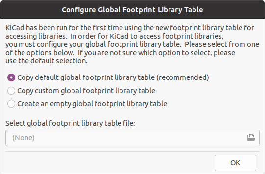
当 Pcbnew 第一次运行时,如果在 KiCad 配置文件夹中没有找到全局封装表文件 fp-lib-table,那么 Pcbnew 将询问如何创建这个文件:
The first option is recommended (Copy default global footprint library table (recommended)). The default footprint library table includes all of the standard footprint libraries that are installed as part of KiCad.
If this option is disabled, KiCad was unable to find the default global footprint library table. This probably means you did not install the standard footprint libraries with KiCad, or they are not installed where KiCad expects to find them. On some systems the KiCad libraries are installed as a separate package.
-
If you have installed the standard KiCad footprint libraries and want to use them, but the first option is disabled, select the second option and browse to the
fp-lib-tablefile in the directory where the KiCad libraries were installed. -
If you already have a custom footprint library table that you would like to use, select the second option and browse to your
fp-lib-tablefile. -
If you want to construct a new footprint library table from scratch, select the third option.
Footprint library management is described in more detail later.
Pcbnew 用户界面
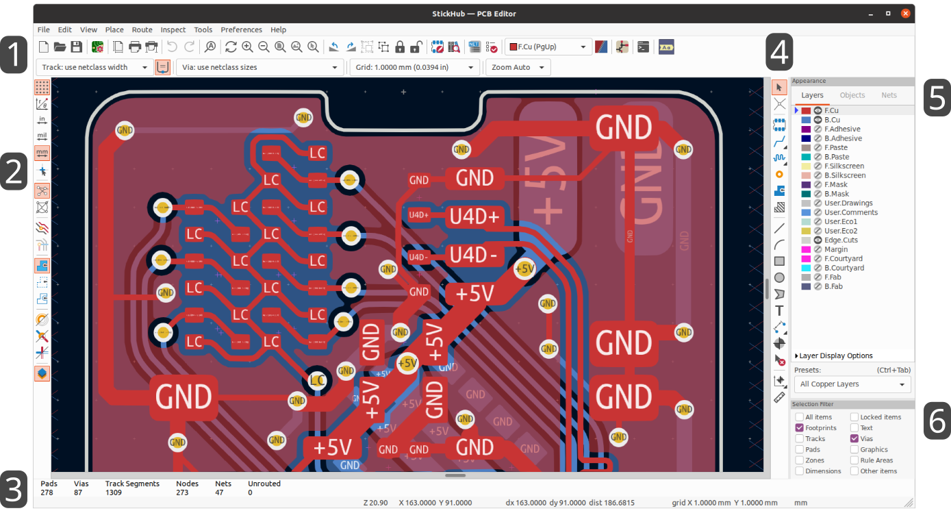
主 Pcbnew 用户界面如上所示,其中指出了一些关键元素:
-
顶部工具栏 (文件管理、缩放工具、编辑工具)
-
左侧工具栏 (显示选项)
-
消息面板和状态栏
-
右侧工具栏 (绘图和设计工具)
-
外观面板
-
选择过滤器面板
导航编辑画布
编辑画布是正在设计的板上的视图。您可以平移和缩放到电路板的不同区域,也可以翻转视图以从底部显示电路板。
By default, dragging with the middle or right mouse button will pan the canvas view and scrolling the mouse wheel will zoom the view in or out. You can change this behavior in the Mouse and Touchpad section of the preferences (see Configuration and Customization for details).
Several other zoom tools are available in the top toolbar:
-
 zooms in on the center of the viewport.
 -
 zooms out from the center of the viewport.
 -
 zooms to fit the frame around the drawing sheet.
 -
 zooms to fit the items within the drawing sheet.
 -
 allows you to draw a box to determine the zoomed area.
The cursor’s current position is displayed at the bottom of the window (X and Y), along with the current zoom factor (Z), the cursor’s relative position (dx, dy, and dist), the grid setting, and the display units.
The relative coordinates can be reset to zero by pressing Space. This is useful for measuring distance between two points or aligning objects.
快捷键
The Ctrl+F1 shortcut displays the current hotkey list. The default hotkey list is included in the Actions Reference section of the manual.
The hotkeys described in this manual use the key labels that appear on a standard PC keyboard. On an Apple keyboard layout, use the Cmd key in place of Ctrl, and the Option key in place of Alt.
Many actions do not have hotkeys assigned by default, but hotkeys can be assigned or redefined using the hotkey editor (Preferences → Preferences… → Hotkeys).
| 通过热键可用的许多操作也可在上下文菜单中使用。要访问上下文菜单,请在编辑画布中单击鼠标右键。根据选择的内容或处于活动状态的工具,将提供不同的操作。 |
Hotkeys are stored in the file user.hotkeys in KiCad’s configuration directory. The location is platform-specific:
-
Windows:
%APPDATA%\kicad\6.0\user.hotkeys -
Linux:
~/.config/kicad/6.0/user.hotkeys -
macOS:
~/Library/Preferences/kicad/6.0/user.hotkeys
KiCad can import hotkey settings from a user.hotkeys file using the Import Hotkeys button in the hotkey editor.
显示和选择控件
板层
Pcbnew 中的层表示线路板上的物理铜层,以及用于定义诸如丝印、阻焊和电路板边缘的图形层。 在编辑器中始终有一个处于活动状态的层。 活动图层被画在其他层之上,并且将是指定给新创建对象的层。 活动图层在顶部工具栏的层选择器下拉框中显示,并在外观面板中也高亮显示。 若要变更活动图层,可以左键单击外观面板中的图层名称、使用顶部工具栏中的下拉图层选择器或使用快捷键。 可以隐藏图层以简化电路板视图。即使层是活动层,也可以隐藏该层。
电路板层的显示顺序
| TODO:写下这一节。 |
外观面板
外观面板提供用于管理 Pcbnew 绘图画布中对象的可见性、颜色和不透明度的控件。它有三个选项卡:图层选项卡包含电路板层的控件,对象选项卡包含不同类型图形对象的控件,网络选项卡包含飞线和铜项外观的控件。
图层控件
在外观面板的图层选项卡中,每个电路板图层都显示了其颜色和可见性状态。 活动图层在色块的左边有一个箭头指示器。 左键点击一个图层来选择它作为活动图层。 左键单击相应的可见性图标,在可见和隐藏之间切换该图层。 双击或中击色块来改变该图层的颜色。
| 必须先在首选参数中创建自定义颜色主题, 然后才能在“外观”面板中更改图层颜色。 |
在图层列表下方是一个包含图层显示选项的可展开面板。第一个设置控制非活动图层的显示方式:正常、暗显或隐藏。层显示模式可用于简化视图并聚焦于单个层。当非活动层显示模式为 "暗显" 或 "隐藏" 时,不能选择非活动层上的项目。您可以使用热键 Ctrl+H 快速切换这些显示模式。
翻转电路板视图 将显示电路板,就像从底部看一样(即,绕 Y 轴镜像)。 此选项也可在视图菜单中使用。
| 翻转电路板视图不会更改可视层顺序,活动层将保持在最前面,其他层按正常顺序紧随其后。 |
对象控件
外观面板的 "对象" 选项卡与 "图层" 选项卡类似。 主要区别在于,有些对象没有颜色设置,而四种类型的对象(布线、过孔、焊盘和敷铜)有不透明度控制滑块。 这里的不透明度设置将与图层颜色中设置的任何不透明度相乘。 默认情况下,所有对象都是完全不透明的,除了敷铜,敷铜被设置为半透明,以使通过填充的敷铜更容易看到对象。
图层预设
图层预设存储了哪些图层和对象是可见和隐藏的,以便于调用。 有几个内置的图层预设,您可以保存您自己的自定义预设。 自定义预设存储在一个电路板的工程设置中,因为预设可能是特定于某个电路板的叠加。
要加载一个预设,请从外观面板底部的预设下拉菜单中选择它,或者通过按住 Ctrl 并按 Tab 来使用快速切换器。 一旦快速切换器窗口出现,你可以按 Tab 和 Shift+Tab 来循环浏览可用的预设。 当你放开 Ctrl 键时,高亮显示的预设将被加载。
要保存一个自定义的预设,首先使用可见性控制来选择你希望哪些图层是可见的,然后从预设下拉菜单中选择保存预设…。 给您的预设一个名字,它现在可以通过下拉菜单和快速切换器使用。 要修改一个自定义预设,请遵循相同的过程,并以相同的名称保存修改后的版本,以覆盖现有的版本。 要删除一个自定义预设,从下拉菜单中选择删除预设…选项,并从列表中选择要删除的预设。
网络和网络类控件
外观面板的网络选项卡显示电路板中所有网络和网络类的列表。每个网都有一个可见性控件,用于控制该网在飞线中的可见性。在飞线中隐藏网络不会改变电路板的连接性,也不会影响设计规则检查器;这只是为了使飞线更容易理解。
每个网络和网络类还可以指定一种颜色。默认情况下,此颜色适用于网络 (或网络类中的所有网络) 的飞线。默认情况下,网络没有颜色;这由色样中的棋盘格图案指示。双击或右键单击网络或网络类颜色样本以设置颜色。
| 默认网络类不能分配颜色, 因为该类中的网络将仅使用颜色主题定义的默认飞线最高颜色。 |
您还可以通过外观面板选择并高亮网络和网络类:右击网络或网络类以在菜单中显示这些选项。
网络类列表下面是一个包含网络显示选项的可扩展面板。第一个选项控制如何应用网络颜色。当选择了“所有”时,属于网络或网络类别的所有铜项 (焊盘、布线、过孔和区域) 都将呈现所选的颜色。当选中“飞线”(默认值)时,只有飞线受网络和网络类别颜色的影响。 当选择“没有”时,网络和网络类颜色被忽略。
第二个选项控制如何绘制飞线。“所有图层”表示将在所有未连接的项目之间绘制飞线。“可见层”意味着不会向隐藏层上的项目绘制任何最新的飞线,即使这些项目是未连接的。
选择和选择筛选器
Selecting items in the editing canvas is done with the left mouse button. Single-clicking on an object will select it and dragging will perform a box selection. A box selection from left to right will only select items that are fully inside the box. A box selection from right to left will select any items that touch the box. A left-to-right selection box is drawn in yellow, with a cursor that indicates exclusive selection, and a right-to-left selection box is drawn in blue with a cursor that indicates inclusive selection.
可以通过在单击或拖动的同时按住快捷键来修改选择操作。单击以选择单个项目时,将应用以下快捷键:
| Modifier Keys (Windows) | Modifier Keys (Linux) | Modifier Keys (macOS) | Selection Effect |
|---|---|---|---|
Shift |
Shift |
Shift |
Add the item to the existing selection. |
Ctrl+Shift |
Ctrl+Shift |
Cmd+Shift |
Remove the item from the existing selection. |
long click |
long click or Alt |
long click or Option |
Clarify selection from a pop-up menu. |
Ctrl |
Ctrl |
Cmd |
Highlight the net of the selected copper item. |
拖动以执行选框时,将应用以下快捷键:
| Modifier Keys (Windows) | Modifier Keys (Linux) | Modifier Keys (macOS) | Selection Effect |
|---|---|---|---|
Shift or Ctrl |
Shift or Ctrl |
Shift or Ctrl |
Add item(s) to the existing selection. |
Ctrl+Shift |
Ctrl+Shift |
Cmd+Shift |
Remove item(s) from the existing selection. |
Pcbnew 窗口右下角的选择过滤器面板控制可以用鼠标选择哪些类型的对象。关闭对不需要的对象类型的选择可以更容易地选择密集电路板中的项目。“所有项目”复选框是打开和关闭其他项目的快捷方式。“锁定的项目”复选框独立于其他复选框,并控制是否可以选择已锁定的项目。您可以在选择过滤器中的任何对象类型上单击鼠标右键以快速更改过滤器,使其仅允许选择该类型的对象。
当一个连接的铜线项目被选中时,你可以使用右键菜单中的 "扩展选择" 命令或热键 U 将选择扩展到同一网络的其他铜线项目。 第一次运行这个命令时,选择将被扩展到最近的焊盘。 第二次,选择将被扩展到所有层上的所有连接项。
Selecting an object displays information about the object in the message panel at the bottom of the window. Double-clicking an object opens a window to edit the object’s properties.
按 Esc 将始终取消当前工具或操作,并返回到选择工具。在选择工具处于活动状态时按 Esc 将清除当前选择。
网络高亮
电气网络(或一组网络)可以在 PCB 编辑器中被高亮显示,以显示该网络是如何在 PCB 上布线的。 通过在 PCB 编辑器中选择要高亮的网络,或者在启用交叉探测高亮时在原理图编辑器中选择相应的网络,可以激活网的高亮(见下文)。 当网络高亮激活时,高亮的网或网将以较亮的颜色显示,所有其他项目将以比正常颜色更暗的颜色显示。
有三种方法可以点击一个或多个网络在 PCB 编辑器中高亮:点击铜对象后使用热键 ` ,使用任何铜对象的上下文菜单,以及外观面板的网络选项卡的上下文菜单。当您按下高亮网络热键时,任何选定铜件的网络将被高亮。如果未选中铜项,则编辑器光标下的铜项的网络将高亮。如果光标下没有铜项目,则任何现有的高亮都将被清除。也可以使用清除高操作 (热键 ~) 清除高亮。
选择一个或多个网络进行高亮时,左侧工具栏上的切换网络高亮显示操作变为启用(也可通过热键 Ctrl+` 访问)。此操作将打开或关闭高亮,而无需选择要高亮的新网络。
从原理图交叉探测
KiCad 允许在原理图和 PCB 之间进行双向交叉探测。 有几种不同类型的交叉探测。
选择交叉探测 允许您在原理图中点击一个符号或引脚,在 PCB (如果存在) 中点击相应的封装或焊盘,反之亦然。 默认情况下,交叉探查将导致显示以交叉探查的项目为中心并缩放到合适的位置。 可以在偏好设置对话框的显示选项部分禁用此行为。
高亮交叉探测 允许您同时高亮原理图和 PCB 中的网络。 如果在偏好设置对话框的显示选项部分中启用了选项 "高亮交叉网络", 则在原理图编辑器中高亮某个网络或总线将导致相应的一个或多个网络在 PCB 编辑器中高亮。
左侧工具栏显示控件
左侧工具栏提供了更改 Pcbnew 中项目显示的选项。
|
打开/关闭栅格显示。 注意: 默认情况下,隐藏网格将禁用网格捕捉。 可以在偏好设置的显示选项部分更改此行为。 |
|
在状态栏中的极坐标和笛卡尔坐标显示之间切换。 |
|
以英寸、密耳或毫米为单位显示/输入坐标和尺寸。 |
|
在全屏和小编辑光标 (十字光标) 之间切换。 |
|
打开/关闭飞线显示。 |
|
在直线型和弧线型飞线之间切换。 |
|
在正常和暗显之间切换非活动层显示模式。 注意: 当非活动层显示模式为暗显或隐藏时,此按钮将突出显示。 在这两种情况下,按下按钮都会将层显示模式更改为正常。 隐藏模式只能通过外观面板中的控件或快捷键 Ctrl+H 进入。 |
|
选择要高亮的网络时,会打开或关闭高亮。 注意: 当没有高亮任何网络时,此按钮将被禁用。 要高亮网络,可使用热键 `, 右击网络中的任何铜对象并从网络工具菜单中选择高亮网络, 或右击外观面板的网络选项卡中列表中的网络。 |
|
显示分区填充区域。 |
|
仅显示区域轮廓。 |
|
将分区填充区域显示为轮廓。 |
|
在填充模式和轮廓模式之间切换焊盘的显示。 |
|
在填充模式和轮廓模式之间切换过孔的显示。 |
|
在填充模式和轮廓模式之间切换布线显示。 |
|
显示敷铜填充区域。 |
|
仅显示敷铜轮廓。 |
|
将敷铜填充区域显示为轮廓。 |
|
在填充模式和轮廓模式之间切换焊盘的显示。 |
|
在填充模式和轮廓模式之间切换过孔的显示。 |
|
在填充模式和轮廓模式之间切换布线显示。 |
|
显示或隐藏编辑器右侧的外观和选择过滤器面板。 |
创建 PCB
基本 PCB 概念
KiCad 中的印刷电路板通常由代表电子元件及其焊盘的 封装、定义这些焊盘如何彼此连接的 网络、形成每个网络中焊盘之间的铜连接的 布线、过孔 和 填充区 以及定义电路板边缘、丝印标记和任何其他所需信息的各种图形形状组成。
KiCad 通常会将 PCB 上的网络信息与相关的原理图保持同步,但也可以直接在 PCB 编辑器中创建和编辑网络。
性能
KiCad 能够创建多达 32 个铜层、14 个技术层 (丝印、阻焊、元件粘合剂、焊膏等) 和 13 个通用绘图层的印刷电路板。
The internal measurement resolution of all objects in KiCad is 1 nanometer, and measurements are stored as 32-bit integers. This means it is possible to create boards up to approximately 4 meters by 4 meters.
KiCad 目前支持每个工程/原理图一个电路板文件。
从原理图开始
Creating a board from a schematic is the recommended workflow for KiCad. When you create a new project, KiCad will generate an empty board file with the same name as the project. To start designing the board after you have created a schematic, simply open the board file. You can do this either from the KiCad project manager, or by clicking the "Open PCB in board editor" button in the schematic editor. To import the schematic design information into the board editor, including footprints and net connections, use the Tools → Update Schematic from PCB… action (F8). You can also use the ![]() icon in the top toolbar.
icon in the top toolbar.
| Update PCB from Schematic is the preferred way to transfer design information from the schematic to the PCB. In older versions of KiCad, the equivalent process was to export a netlist from the Schematic Editor and import it into the Board Editor. It is no longer necessary to use a netlist file. |
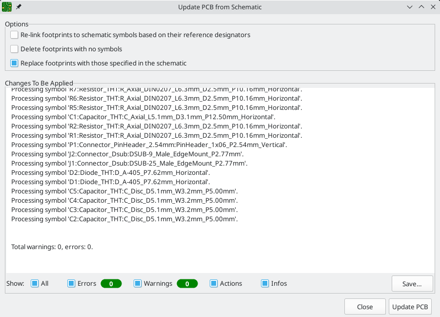
The tool adds the footprint for each symbol to the board and transfers updated schematic information to the board. In particular, the board’s net connections are updated to match the schematic.
The changes that will be made to the PCB are listed in the Changes To Be Applied pane. The PCB is not modified until you click the Update PCB button.
You can show or hide different types of messages using the checkboxes at the bottom of the window. A report of the changes can be saved to a file using the Save… button.
选项
The tool has several options to control its behavior.
| Option | Description |
|---|---|
Re-link footprints to schematic symbols based on their reference designators |
Footprints are normally linked to schematic symbols via a unique identifier created when the symbol is added to the schematic. A symbol’s unique identifier cannot be changed. If checked, each footprint in the PCB will be re-linked to the symbol that has the same reference designator as the footprint. If unchecked, footprints and symbols will be linked by unique identifier as usual, rather than by reference designator. Each footprint’s reference designator will be updated to match the reference designator of its linked symbol. This option should generally be left unchecked. It is useful for specific workflows that rely on changing the links between schematic symbols and footprints, such as refactoring a schematic for easier layout or replicating layout between identical channels of a design. |
Delete footprints with no symbols |
If checked, any footprint in the PCB without a corresponding symbol in the schematic will be deleted from the PCB. Footprints with the "Not in schematic" attribute will be unaffected. If unchecked, footprints without a corresponding symbol will not be deleted. |
Replace footprints with those specified in the schematic |
If checked, footprints in the PCB will be replaced with the footprint that is specified in the corresponding schematic symbol. If unchecked, footprints that are already in the PCB will not be changed, even if the schematic symbol is updated to specify a different footprint. |
从头开始
也可以创建没有匹配原理图的电路板,尽管此工作流程有一些限制,不建议大多数用户使用。为此,您必须独立启动 PCB 编辑器(而不是从 KiCad 工程管理器启动)。在开始设计之前,最好保存电路板文件,该文件还将创建一个工程文件来存储电路板设置。使用 "另存为…" 从文件菜单选择保存电路板文件的位置。将在您选择保存电路板文件的相同位置创建一个同名的工程文件。
电路板设置
在开始您的线路板设计之前,使用电路板设置对话框来配置电路板的基本参数。要打开电路板设置,请单击顶部工具栏中的 ![]() 图标或选择 "电路板设置…" 从文件菜单中选择。
图标或选择 "电路板设置…" 从文件菜单中选择。
配置电路板压层和物理参数
在电路板设置中有两个部分用于配置电路板的压层和层。电路板编辑器层部分用于启用或禁用技术 (非铜) 层,并在需要时为层指定自定义名称。物理压层部分用于配置铜层的数量,以及铜层和介质层的物理参数,例如厚度和材料类型。
要配置电路板的压层,从物理压层部分开始:
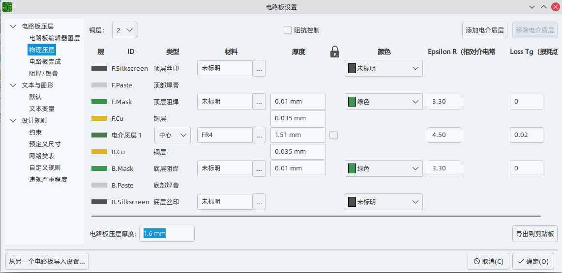
在左上角设置铜层的数量,然后根据需要输入压层的物理参数。 这些参数可以保留其默认值,但请注意,在导出电路板的 3D 模型时,将使用电路板的厚度值,所以如果你打算使用这个功能,最好确保压层厚度是正确的。
| KiCad 目前仅支持铜层数为偶数的压层。 要创建具有奇数层的设计 (例如,柔性印刷电路板或金属芯印刷电路板), 只需选择下一个最高的偶数,而忽略多余的层。 |
接下来,如果需要,可以使用电路板编辑器层部分重命名或隐藏您不会在设计中使用的非铜层。例如,如果您不打算在设计中使用背面丝印,请取消选中 B.Silkcreen 层旁边的复选框。
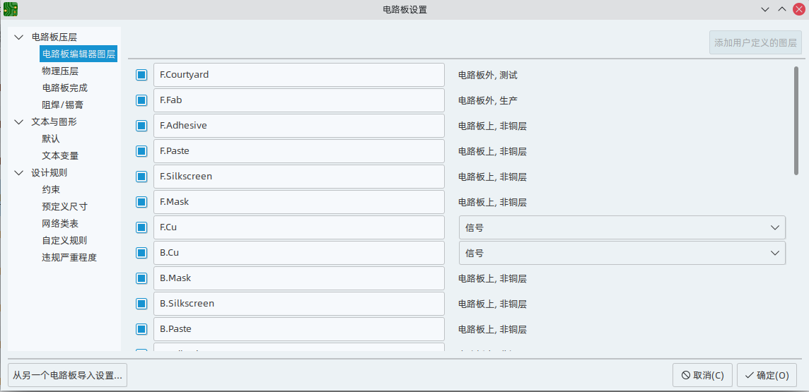
| 在电路板编辑器层部分,可以将铜层指定为信号层、电源层、混合层或跳线层。 本指南仅供用户参考。 无论在此对话框中将类型配置为什么,都可以在任何铜层上布线和敷铜。 |
在电路板编辑器对话框的电路板完成和阻焊/锡膏部分可以找到一些其他的电路板压层设置。电路板完成部分包含用于定义铜电镀和特殊功能 (如镶边或边缘电镀) 的设置。请注意,这些设置目前只影响作为 Gerber 作业文件一部分的电路板属性输出。
阻焊/锡膏部分允许全局调整电路板上焊盘的铜形和阻焊/锡膏形之间的间隙(正或负)。 这些值将被添加到在个别封装或焊盘上设置的任何间隙覆盖。 正的间隙值将导致阻焊层或锡膏开口的形状比铜的形状 更大。 负的间隙值将导致开口比铜的形状 更小。
| 大多数商业 PCB 制造商希望这些值为零,并在 CAM 过程中自行调整阻焊和粘贴开口。 通常最好将这些值保留为默认值零, 除非您自己制作 PCB, 或者您的制造商有具体建议使用不同的值。 |
配置默认文本和图形设置
电路板设置对话框的文本和图形默认值部分可用于配置将用于放置在电路板上的新文本和图形形状的属性。
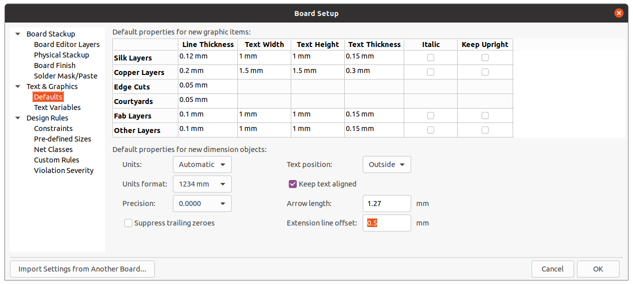
可以为对话框中显示的六种不同类别的图层配置线粗细、文字大小和文字外观。此外,可以为所有图层配置标注对象的特性。有关标注属性的更多详细信息,请参阅下面的标注部分。
文本替换变量可以在文本变量部分创建。 这些变量允许你将变量名称替换为任何文本字符串。 这种替换发生在变量名称在 ${VARIABLENAME} 的变量替换语法内的任何地方。
例如,您可以创建一个名为 VERSION 的变量,并将文本替换设置为 1.0。 现在,在 PCB 上的任何文本对象中,你可以输入 ${VERSION},KiCad 将替代 1.0'。 如果你把替换改为 `2.0',每个包括 `${VERSION} 的文本对象都会自动更新。 你也可以混合使用普通文本和变量。 例如,你可以创建一个文本对象,内容为 版本:${VERSION},它将被替换为 版本:1.0。
配置设计规则
设计规则控制交互式布线器的行为、覆铜的填充和设计规则检查器。设计规则可以随时修改,但我们建议您在电路板设计过程开始时建立所有已知的设计规则。
约束
基本设计规则是在电路板设置对话框的约束条件部分中配置。 这一部分的约束条件适用于整个板子,应该设置为板子制造商推荐的值。 这里设置的任何最小值都是一个 绝对(absolute) 的最小值,不能被更具体的设计规则所覆盖。 例如,如果你需要电路板的一部分的铜间隙为 0.2mm,其余部分为 0.3mm,你必须在约束条件部分输入 0.2mm 的最小铜间隙,并使用网络类或自定义规则来设置较大的 0.3mm 间隙。
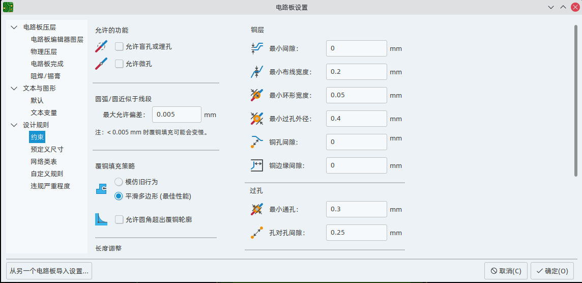
除了设置最小间隙外,还可以在此处配置许多功能:
| 设置 | 描述 |
|---|---|
允许盲孔/埋孔 |
必须先启用此设置,然后才能使用布线器放置盲孔或埋孔。 盲孔是机械钻孔,从外层铜层之一开始,到内层之一结束。 埋孔是机械钻孔,在内部铜层开始和结束。 |
允许微孔 |
在使用布线器放置微孔之前,必须启用此设置。 微孔是典型的激光钻孔,将外层铜层连接到相邻的内层。 KiCad 支持单独的微孔尺寸限制,因为它们通常比机械钻孔的埋孔小。 |
由线段近似的圆弧/圆 |
在某些情况下,KiCad 必须使用一系列直线段来近似圆形,如圆弧和圆的形状。 此设置控制此近似所允许的最大误差:换句话说,这些线段之一上的点与圆弧或圆的真实形状之间的最大距离。 将其设置为比默认值 0.005mm 更小的数字将产生更平滑的形状,但在较大的电路板上可能会非常慢。 默认值通常会导致由于制造公差而在制造的电路板中无法检测到的圆弧近似误差。 |
敷铜填充策略 |
KiCad 的敷铜填充算法进行了改进,获得了更好的结果和更快的性能。 新算法产生的结果与旧算法略有不同,因此此设置允许保留旧行为, 以防止在最新版本的 KiCad 中打开旧设计时产生不同的 Gerber 输出。 我们建议对所有新设计使用平滑多边形模式。 |
允许圆角超出敷铜轮廓 |
敷铜可以在敷铜属性对话框中添加圆角 (圆角)。 默认情况下,不允许在敷铜轮廓之外使用敷铜 (包括圆角)。 这实际上意味着,即使配置了圆角,也不会对敷铜轮廓的内角进行圆角处理。 通过启用此设置,敷铜轮廓的内角将被圆角,即使这会导致敷铜中的铜延伸到敷铜轮廓之外。 |
在布线长度计算中包括压层高度 |
默认情况下,压层的高度用于计算从一层到另一层通过过孔的布线的附加长度。 此计算依赖于正确配置的电路板压层高度。 在某些情况下,最好忽略过孔的高度,假设过孔没有增加长度,则只计算布线长度。 禁用此设置将从布线长度计算中排除过孔长度。 |
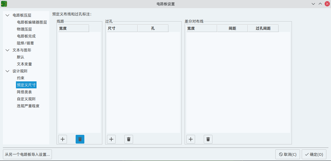
预定义大小
预定义的尺寸部分允许你定义你希望在布线时可用的布线和过孔尺寸。 网络类可以用来定义不同网络中的布线和过孔的默认尺寸(见下文),但是在这个部分定义一个尺寸列表,可以让你在布线的时候逐步了解这些尺寸。 例如,你可能希望电路板上的默认布线宽度是 0.2 mm,但对于一些承载更多电流的部分使用 0.3 mm,而对于一些空间有限的部分使用 0.15 mm。 您可以在电路板设置对话框中定义这些布线的宽度,然后在布线时在它们之间切换。
网络类
网络类部分允许你为不同网类配置布线和清除规则。 在 KiCad 中,每个网络都是一个网络类的一部分。 如果你不把一个网络添加到一个特定的类中,它将是默认类的一部分,它总是存在。 飞线可以通过原理图设置和电路板设置对话框从原理图或 PCB 编辑器中添加到网络类。
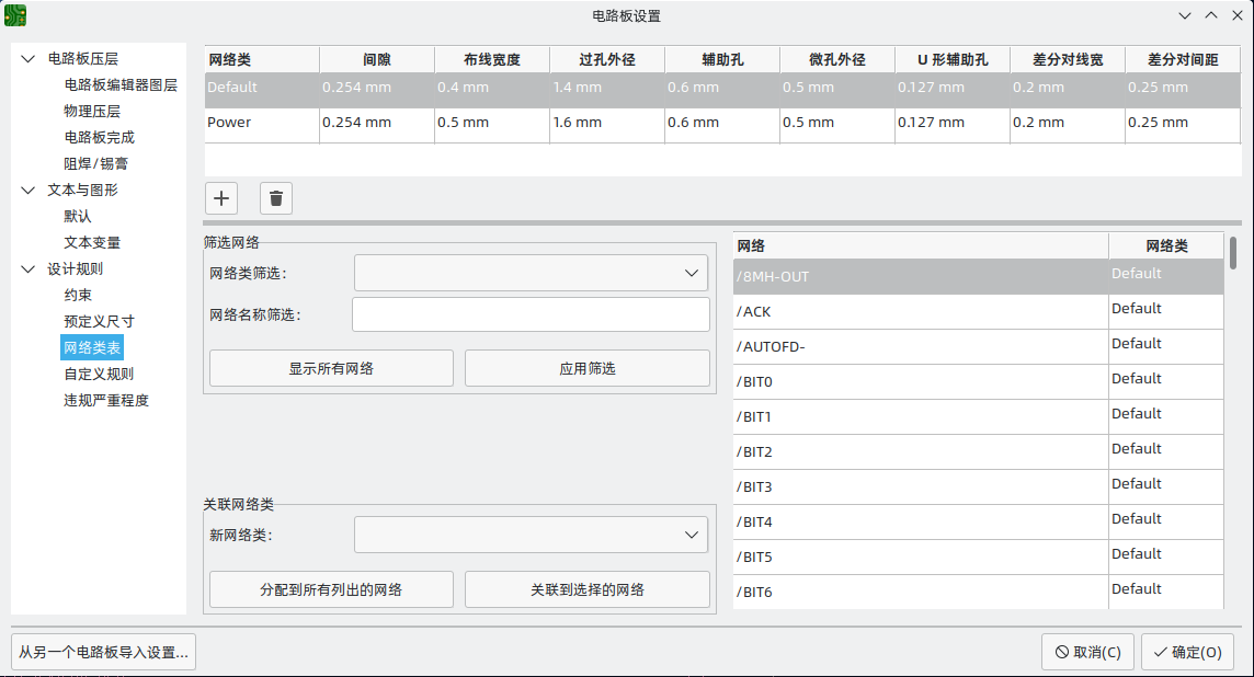
网络类部分的上部包含一个表格,显示了适用于每个网络类的设计规则。 每个网络类都有铜间隙、布线宽度、过孔尺寸和差分对尺寸的值。 这些值将在创建布线和过孔时使用,除非有更具体的规则覆盖它们(见下面的自定义规则)。
任何规则都不能覆盖电路板设置的约束条件部分中设置的最小值。
例如,如果您将网络类间距设置为 0.1 mm,但约束条件部分中的最小间距设置为 0.2 mm,
则该类网络的间距将为 0.2 mm。
|
当 PCB 编辑器中的布线宽度和过孔尺寸控制设置为 "使用网络类值" 时,就会使用为每个网络类定义的布线宽度和过孔尺寸。 这些宽度和尺寸被认为是该网络类的默认或最佳尺寸。 它们不是最小或最大值。 手动将布线宽度或过孔尺寸改为与网络类部分定义的不同的值,不会导致违反 DRC。 要将布线宽度或过孔大小限制在特定的值,请使用自定义规则。
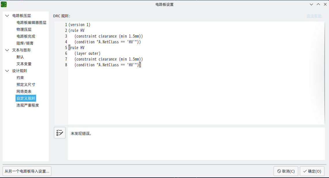
自定义规则
自定义规则部分包含一个文本编辑器,用于使用自定义规则语言创建设计规则。 自定义规则用于创建基本约束或网络类设置没有涵盖的特定设计规则检查。
只有在自定义规则定义中没有错误时,才会应用自定义规则。 在关闭电路板设置之前,使用检查规则语法器按钮来测试定义并修复任何问题。
请参阅高级主题一章中的自定义设计规则,了解关于自定义规则语言的更多信息以及规则实例。
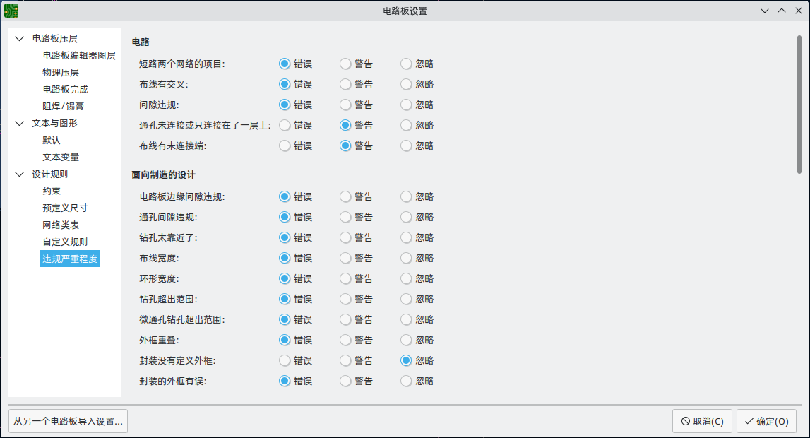
违规严重程度
违规严重性部分允许你配置每种设计规则检查的严重性。 每条规则可以被设置为创建一个错误标记、一个警告标记或没有标记(忽略)。
| 在设计规则检查器中可能会忽略个别规则违规。 在违规程度部分中将规则设置为忽略将完全禁用相应的设计规则检查。 请谨慎使用此设置。 |
正在导入设置
您可以从现有电路板导入部分或全部电路板设置。此技术可用于创建具有您想要在多个设计上使用的设置的 "模板" 电路板,然后将这些设置从模板电路板导入到每个新电路板中,而不是手动输入。
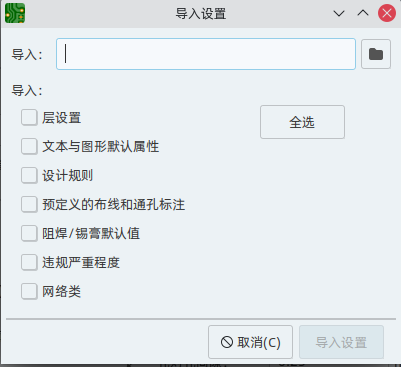
要导入设置,请点击电路板设置对话框底部的 从另一个电路板导入设置… 按钮,然后选择您要导入的 kicad_pcb 文件。 选择你想导入的设置,当前的设置将被选定的板子的值覆盖。
编辑电路板
放置和绘制操作
放置和绘图工具位于右边的工具栏中。 当一个工具被激活时,它将一直处于激活状态,直到选择了一个不同的工具或用 Esc 键取消该工具。 当任何其他工具被取消时,选择工具总是被激活。
某些工具栏按钮在调色板中有多个可用工具。这些工具由按钮右下角的小箭头表示:
要显示调色板,你可以在工具上点击并按住鼠标按钮,或者点击并拖动鼠标。 调色板关闭时将显示最近使用的工具。
|
Selection tool (the default tool). |
|
Local ratsnest tool: when the board ratsnest is hidden, selecting footprints with this tool will show the ratsnest for the selected footprint only. Selecting the same footprint again will hide its ratsnest. The local ratsnest setting for each footprint will remain in effect even after the local ratsnest tool is no longer active. |
|
Footprint placement tool: click on the board to open the footprint chooser, then click again after choosing a footprint to confirm its location. |
|
Route tracks / route differential pairs: These tools activate the interactive router and allow placing tracks and vias. The interactive router is described in more detail in the Routing Tracks section below. |
|
Tune length: These tools allow you to tune the length of single tracks or the length or skew of differential pairs, after they have been routed. See the Routing Tracks section for details. |
|
Add vias: allows placing vias without routing tracks. Vias placed on top of tracks using this tool will take on the net of the closest track segment and will become part of that track (the via net will be updated if the pads connected to the tracks are updated). Vias placed anywhere else will take on the net of a copper zone at that location, if one exists. These vias will not automatically take on a new net if the net of the copper zone is changed. |
|
Add filled zone: Click to set the start point of a zone, then configure its properties before drawing the rest of the zone outline. Zone properties are described in more detail below. |
|
Add rule area: Rule areas, formerly known as keepouts, can restrict the placement of items and the filling of zones and can also define named areas to apply specific custom design rules to. |
|
Draw lines. Note: Lines are graphical objects and are not the same as tracks placed with the Route Tracks tool. Graphical objects cannot be assigned to a net. |
|
Draw arcs: pick the center point of the arc, then the start and end points. |
|
Draw rectangles. Rectangles can be filled or outlines. |
|
Draw circles. Circles can be filled or outlines. |
|
Draw graphical polygons. Polygons can be filled or outlined. Note: Filled graphical polygons are not the same as filled zones: graphical polygons cannot be assigned to a net and will not keep clearance from other items. |
|
Add text. |
|
Add dimensions. Dimension types are described in more detail below. |
|
Add layer alignment mark. |
|
Deletion tool: click objects to delete them. |
|
Set drill/place origin. Used for fabrication outputs. |
|
Set grid origin. |
捕捉
移动、拖动和绘制电路板元素时,栅格、焊盘和其他元素可以具有捕捉点,具体取决于用户偏好设置中的设置。在复杂的设计中,捕捉点可能离得太近,这会使当前的工具操作变得困难。使用下表中的快捷键可以在移动鼠标时禁用栅格和对象捕捉。
| 快捷键 | 效果 |
|---|---|
Ctrl |
关闭网格捕捉。 |
Shift |
关闭对象捕捉。 |
编辑对象属性
所有对象都有可在对话框中编辑的属性。 使用热键 E 或从右键菜单中选择属性来编辑所选项目的属性。 只有当你选择的所有项目都是同一类型时,你才能打开属性对话框。 要想一次编辑不同类型的项目的属性,请参阅下面关于批量编辑工具的章节。
在属性对话框中,任何包含数字值的字段也可以接受一个基本的数学表达式,从而得到一个数字值。 例如,一个尺寸可以被输入为 2 * 2mm,结果是 4mm 的值。 支持基本算术运算符以及用于定义运算顺序的圆括号。
使用封装
| TODO: 编写这一节—包括封装属性,从库中更新,等等。 |
使用焊盘
The properties of each individual pad of a footprint can be inspected and edited after placing the footprint on the board. In other words, it is possible to override the design of an individual footprint pad in a specific instance of the footprint on the board, if the footprint design in the library is not appropriate. For example, you may wish to remove the solder paste aperture for a pad that needs to remain unsoldered in a specific design, or you may wish to move the location of a through-hole pad for an axial-lead resistor in order to fit a specific design.
| By default, the position of all footprint pads are locked, so it is possible to edit the pad properties but not move the pad’s location relative to the rest of the footprint. Pads may be unlocked to allow free movement, which can be useful for certain applications (such as through-hole footprints with varying lead positions) but is generally never recommended for surface-mount footprints. |
The pad properties dialog is opened through the context menu or default hotkey E when a pad is selected. Note that KiCad assumes that if you click near a pad, you are probably trying to select the entire footprint rather than a single pad. To select a single pad, make sure to click inside the pad area, or turn off the Footprints setting in the selection filter (and make sure the Pads setting is turned on) to prevent accidental selection of the entire footprint rather than a specific pad.
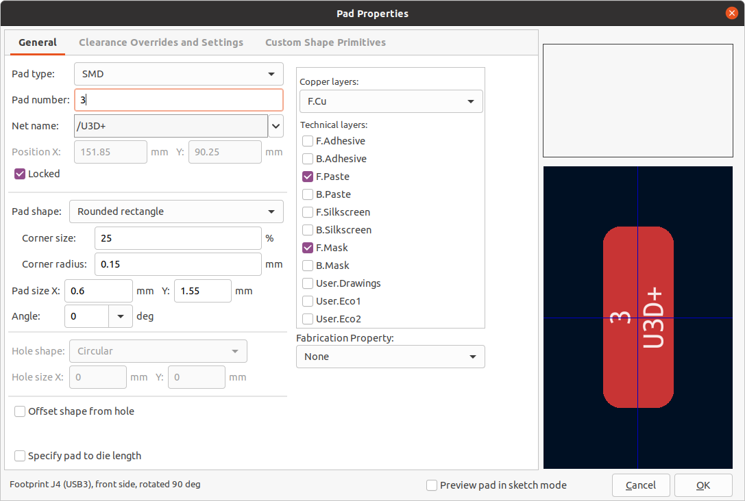
The General tab of the pad properties dialog shows the physical properties of the pad, including its geometry, shape, and layer settings.
Pad type: this setting controls which features are enabled for the pad:
SMD pads are electrically-connected and have no hole. In other words, they exist on a single copper layer.
Through-hole pads are electrically-connected and have a plated hole. The hole exists on every layer, and the copper pad exists on multiple layers (see Copper layers setting below).
Edge Connector pads are SMD pads that are allowed to overlap the board outline on the Edge.Cuts layer.
NPTH, Mechanical pads are non-plated through holes that do not have an electrical connection.
SMD Aperture pads are pads that have no hole and no electrical connection. These can be used to add specific designs to a technical layer, for example a paste or solder mask aperture.
The Copper layers setting controls which copper layers will have a shape associated with the pad.
For SMD pads, the options are F.Cu or B.Cu, controlling whether the pad sits on the front or the back of the board relative to the footprint’s location. In other words, if a pad is set to exist on B.Cu in its properties, and the footprint is flipped to the back of the board, that pad will now exist on F.Cu, because it also has been flipped.
For through-hole pads, it is possible to remove the pad shape from copper layers where the pad is not electrically connected to other copper (tracks or filled zones). Setting the copper layers to connected layers only will remove the pad shape from any unconnected layers, and setting to F.Cu, B.Cu, and connected layers will remove the pad shape from any internal unconnected layers. This can be useful in dense board designs to increase the routable area on internal layers.
The Technical layers checkboxes control which technical layers will have an aperture added with the pad’s shape. By default, pads have apertures on the paste and mask layers matching their copper layer.
| It is not possible to define a different pad shape or size on different copper layers in the current version of KiCad. |
Specify pad to die length: This setting allows a length to be associated with this pad that will be added to the routed track length by the track length tuning tools and the Net Inspector. This can be used to specify internal bondwire lengths for more accurate length matching, or in other situations where the electrical length of a net is longer than the length of the routed tracks on the board.
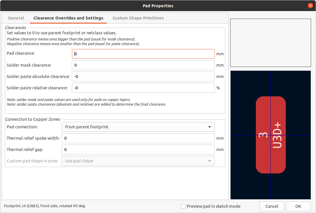
The aperture appearing on any technical layer will have the same shape and size as the pad shape on the copper layer(s). In the PCB manufacturing process, the manufacturer will often change the relative size of mask and paste apertures relative to the copper pad size, but since this size change is specific to a manufacturing process, most manufacturers expect the design data to be provided with the apertures set to the same size as the copper pads. For specific situations where you need to oversize or undersize a technical layer aperture in the design data, you can use the settings in the Overrides tab.
Pad clearance controls the minimum clearance between the pad and any copper shape (tracks,
vias, pads, zones) on a different net. This value is normally set to 0 which will cause the pad
clearance to be inherited from any clearance override set on the footprint, or the board’s design
rules and netclass rules if the footprint clearance is also set to 0.
Solder mask clearance controls the size difference between the pad shape and the aperture shape
on the F.Mask and B.Mask layers. A positive number means the solder mask aperture will be larger
than the copper shape. This number is an inflation applied to all directions. For example, a
value of 0.1mm here will cause the solder mask aperture to be inflated by 0.1mm, meaning that
there will be an 0.1mm border on all sides of the pad and the solder mask opening will be 0.2mm
wider than the pad when measured along a given axis.
Solder paste absolute clearance controls the size difference between the pad shape and the aperture shape on the F.Paste and B.Paste layers. Its behavior is otherwise identical to the behavior of the solder mask clearance setting.
Solder paste relative clearance allows setting a solder paste clearance value as a percentage of the pad size rather than an absolute distance value. If both relative and absolute clearances are specified, they are added together to determine the solder paste aperture size.
The Overrides tab also has controls for how the pad connects to any copper zone that overlaps it and shares its net.
Pad connection controls whether the pad will have a solid, thermal relief, or no connection to the zone. Like the other overrides, this one may be set for an individual pad or for an entire footprint. The default setting for this control is From parent footprint, and the default footprint setting is to use the connection mode specified in the zone properties.
Thermal relief spoke width controls the width of the spokes generated when the zone connection mode is Thermal Relief.
Thermal relief gap controls the length of the thermal spokes, or the gap between the pad’s shape and the filled copper area of the zone.
Custom pad shape in zone controls the behavior of the zone filler when the pad uses a custom shape rather than one of the default shapes. This can be used to achieve different results when using thermal reliefs and custom pad shapes.
使用区域
Copper zones, also sometimes called copper pours or fills by other EDA tools, are solid or hatched areas of copper assigned to a particular net that automatically keep clearance from other copper objects. Zones are commonly used to fill in all free space on a board layer (or a portion of a layer) in order to create ground and power planes, carry high currents, or to provide shielding.
| Some EDA tools have separate tools for creating "plane layers" and for creating copper zones on signal layers. In KiCad, the Copper Zone tool is used for both these applications. |
Zones are defined by a polygonal outline that defines the maximum extent of the filled copper area. This outline does not represent physical copper and will not appear in exported manufacturing data. The actual copper areas of the zone must be filled each time the outline, or any objects inside the outline, are modified. The filling process may be run on a single zone, or on all zones in a board (default hotkey B). Zones may be unfilled (default hotkey Ctrl+B) to improve performance and reduce visual clutter while editing large boards.
| Zone filling is a manual process rather than occurring every time an object changes that would result in a change to the zone copper. This is because zone filling can be a slow process on older computers or very large designs. It is important to make sure zone fills are up-to-date before generating outputs. KiCad will check that zones have been updated and warn you before generating outputs or running DRC when zones have not yet been refilled. |
To draw a zone, click the Add Filled Zone tool (![]() ) on the right toolbar, or use default hotkey Ctrl+Shift+Z. Click to choose the first point of the zone outline. The Zone Properties dialog will appear, allowing you to choose the zone net and other properties. These properties may be edited at any time, so it is not critical to choose them all correctly at first. Accept the dialog and continue placing points to define the zone outline. To finish the zone, double-click to set the last point. Zone outline points may be modified like graphic polygons, by dragging the square handles to move a corner or dragging the circular handles to move an edge. To edit the zone’s properties, use hotkey E or select Properties from the context menu.
) on the right toolbar, or use default hotkey Ctrl+Shift+Z. Click to choose the first point of the zone outline. The Zone Properties dialog will appear, allowing you to choose the zone net and other properties. These properties may be edited at any time, so it is not critical to choose them all correctly at first. Accept the dialog and continue placing points to define the zone outline. To finish the zone, double-click to set the last point. Zone outline points may be modified like graphic polygons, by dragging the square handles to move a corner or dragging the circular handles to move an edge. To edit the zone’s properties, use hotkey E or select Properties from the context menu.
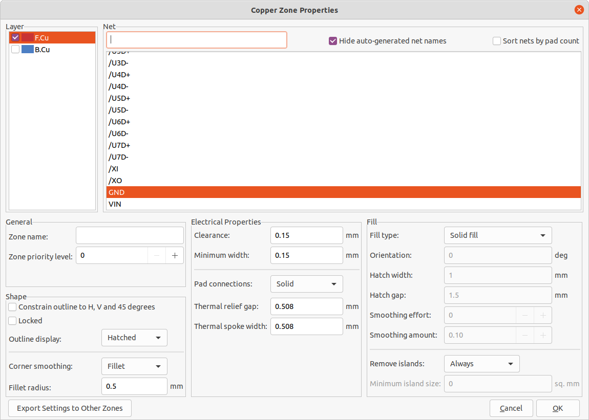
Layer: A single zone object can create filled copper on one or more copper layers. Check the box next to each copper layer that this zone outline should fill on. The copper on each layer will be filled independently, but all layers will share the same net.
Net: Select the electrical net that the zone copper should be connected to. It is possible to create zones with no net assignment. Zones with no net will keep clearance from any copper objects on any net.
Zone name can be used to assign a specific name to a zone. This name can be used to refer to the zone in custom DRC rules.
Zone priority level determines the order in which multiple zones on a single layer are filled. The highest priority level zone on a given layer will be filled first. Lower-priority zones will keep clearance to the filled areas of higher-priority zones. Two zones on the same layer with the same priority level will overlap (short-circuit) with each other.
| Zones with the same priority level will never keep clearance from each other, even if they are assigned to different nets! The design rule checker will report these short-circuits, but they will not be prevented by the zone filler. |
Constrain outline to H, V and 45 degrees controls the initial behavior of the zone outline drawing tool. When this option is enabled, the zone outline will be restricted to 45-degree angles. Note that after the zone outline has been created, this option has no effect. Outline points may be modified freely after creation.
Locked controls whether or not the zone outline object is locked. Locked objects may not be manipulated or moved, and cannot be selected unless the Locked Items option is enabled in the Selection Filter panel.
Outline display controls how the zone outline is drawn on screen. In Line mode, only the border lines of the outline are drawn. In Hatched mode, hatch lines are drawn on the inside of the outline border for a short distance, to make the zone outline more apparent. In Fully Hatched mode, hatch lines are drawn across the entire inside of the zone outline.
Corner smoothing controls the behavior of the filled copper areas at corners of the outline. Corners can be smoothed by a chamfer or fillet, or can extend all the way to the outline corner if smoothing is disabled.
| By default, chamfers and fillets are not added to inside corners of the zone outline, because this would result in filled copper extending outside the outline. If smooth inside corners are desired, enable the Allow fillets outside zone outline option in the Constraints section of the Board Setup dialog. |
Clearance controls the minimum clearance the filled areas of this zone will keep from other copper objects. Note that if two clearance values are in conflict, the larger clearance value will be used. For example, if a zone is set to use 0.2mm clearance but its netclass is set to use 0.3mm clearance, the result will be an 0.3mm clearance.
Minimum width controls the minimum size of narrow necks of copper created inside the zone. Any copper areas that would be below this minimum width are removed during the filling process.
Pad connection controls the way that the filled zone areas will connect to footprint pads on the same net. Solid connections will result in the copper completely overlapping the pads. Thermal reliefs will result in small copper spokes connecting the pad to the rest of the copper zone, increasing the thermal resistance between the pad and the rest of the zone. This can be useful for hand soldering. Reliefs for PTH will apply thermal reliefs to plated through-hole pads and use solid connections for surface mount pads. None will result in the zone not connecting to any pads on the same net.
Thermal relief gap controls the distance maintained between any pad and the copper zone when the pad connection mode is set to generate thermal reliefs.
Thermal spoke width controls the width of the "spokes", or short copper segments connecting the pad to the rest of the copper zone.
Fill type controls how the copper zone is filled: the default is solid fill, which will result in copper filling in all available space within the zone outline. The zone can also be set to fill a hatch pattern, which will fill the area with a pattern that contains less copper. This can be useful for flexible printed circuits and other specialty applications.
Orientation controls the angle of the hatch pattern lines. An orientation of 0 degrees will result in the hatch pattern using horizontal and vertical lines.
Hatch width controls the width of each line in the hatch pattern.
Hatch gap controls the distance between each line in the hatch pattern.
Smoothing effort controls the style of smoothing applied to the hatch pattern. A value of 0 will result in no smoothing, and a value of 3 will result in the finest smoothing. Higher values will result in longer processing time and larger Gerber files.
Smoothing amount is a ratio that controls the size of the smoothing chamfers or fillets that are generated when smoothing effort is set to a value other than 0. An amount of 0.0 results in no smoothing, and a value of 1.0 results in maximum smoothing (in other words, a chamfer or fillet equal to half of the hatch gap).
Remove islands controls the behavior of isolated copper areas, also called islands, after the initial zone fill. When this is set to always, isolated areas inside the zone are removed. When set to never, isolated areas are left alone, and will result in copper areas that are not connected to the rest of the net. When set to below area limit, a minimum island size can be specified, and islands below this threshold will be removed.
图形对象
图形对象 (直线、圆弧、矩形、圆、多边形和文本)可以存在于任何图层上,但不能分配给网络。矩形、圆和多边形可以在其属性对话框中设置为填充或轮廓。线宽属性将控制轮廓的宽度,即使是填充形状也是如此。填充形状的线宽可以设置为 "0" 以禁用轮廓。
正在创建图形形状
The right toolbar can be used to create lines (![]() , default hotkey Ctrl+Shift+L), arcs (
, default hotkey Ctrl+Shift+L), arcs (![]() , default hotkey Ctrl+Shift+A), rectangles (
, default hotkey Ctrl+Shift+A), rectangles (![]() ), circles (
), circles (![]() , default hotkey Ctrl+Shift+C), and polygons (
, default hotkey Ctrl+Shift+C), and polygons (![]() , default hotkey Ctrl+Shift+P).
, default hotkey Ctrl+Shift+P).
Rectangles, circles, and polygons can be filled shapes or outlines. The line width option controls the width of the outline. The outline width extends on both sides of the "ideal" shape of the graphic object. For example, a graphic circle that is defined to have 2mm radius and 0.2mm line width will consist of a torus with an outer radius of 2.2mm and inner radius of 1.8mm. If the filled shape option is enabled and the line width is set to 0, the shape will be a filled circle with 2mm radius.
正在创建文本对象
Graphical text may be placed by using the (![]() ) icon in the right toolbar or by keyboard shortcut Ctrl+Shift+T. Click to place the text origin, and then edit the text and its properties in the dialog that will appear:
) icon in the right toolbar or by keyboard shortcut Ctrl+Shift+T. Click to place the text origin, and then edit the text and its properties in the dialog that will appear:
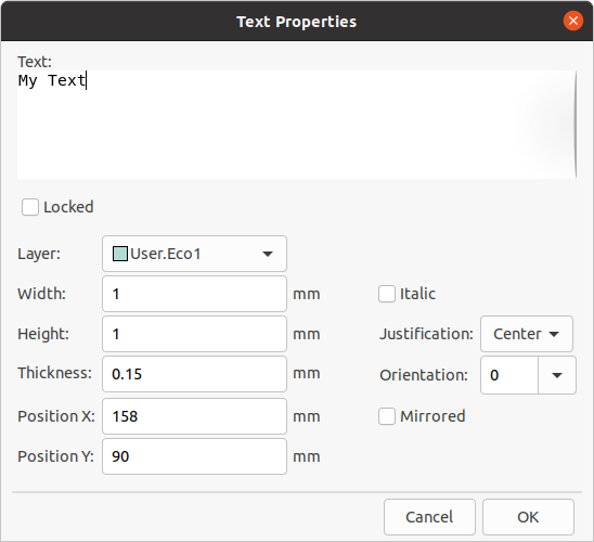
Text may be placed on any layer, but note that text on copper layers cannot be associated with a net and cannot form connections to tracks or pads. Copper zones will fill around the rectangular bounding box of text objects.
电路板轮廓 (边缘切割)
KiCad 使用 Edge.Cuts 层上的图形对象来定义电路板的轮廓。 该轮廓必须是一个连续(封闭)的形状,但可以由不同类型的图形对象组成,如线和弧,或者是一个单一的对象,如矩形或多边形。 如果没有定义电路板的轮廓,或者电路板的轮廓无效,那么一些功能,如 3D 查看器和一些设计规则的检查将无法发挥作用。
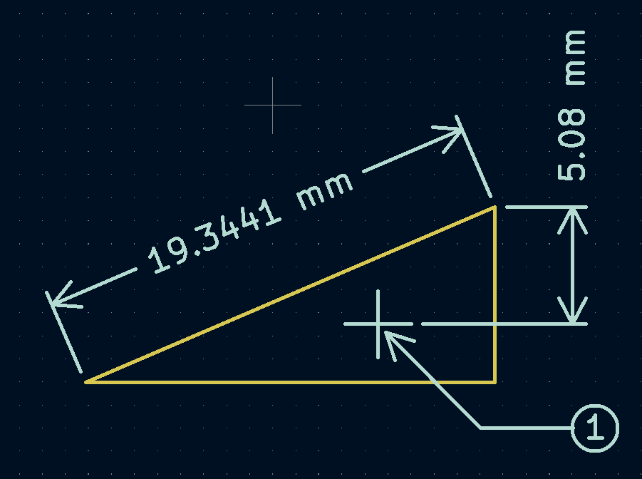
标注
标注是用于显示测量值或电路板设计上的其他标记的图形对象。 它们可以被添加到任何绘图层中,但通常被添加到用户层之一。 KiCad 目前支持四种不同类型的标注:对齐、正交、中心和引线。
对齐 标注 (![]() ) 表示两点之间距离的测量。
测量轴是连接这两个点的线,标注图形与该轴保持平行。
) 表示两点之间距离的测量。
测量轴是连接这两个点的线,标注图形与该轴保持平行。
正交 标注 (![]() ) 也测量两点之间的距离,但测量轴是 X 轴或 Y 轴。
换句话说,这些标注表示两点之间距离的水平或垂直分量。
创建正交标注时,在选择要测量的两个点后,可以根据放置标注的位置选择要用作测量轴的轴。
) 也测量两点之间的距离,但测量轴是 X 轴或 Y 轴。
换句话说,这些标注表示两点之间距离的水平或垂直分量。
创建正交标注时,在选择要测量的两个点后,可以根据放置标注的位置选择要用作测量轴的轴。
中心 标注 (![]() ) 创建一个十字标记来指示一个点或圆或圆弧的圆心。
) 创建一个十字标记来指示一个点或圆或圆弧的圆心。
引线 标注 (![]() ) 创建一个箭头,将一条引线连接到文本字段。
此文本字段可以包含任何文本以及文本周围的可选圆形或矩形框。
这种类型的标注通常用来提醒人们注意设计的某些部分,以便在制造说明中参考。
) 创建一个箭头,将一条引线连接到文本字段。
此文本字段可以包含任何文本以及文本周围的可选圆形或矩形框。
这种类型的标注通常用来提醒人们注意设计的某些部分,以便在制造说明中参考。
创建一个标注后,可以编辑其属性(热键 E)以改变显示数字的格式以及文本和图形线的风格。
| 您可以在电路板设置对话框的文本和图形默认值部分自定义新创建的标注对象的默认样式。 |
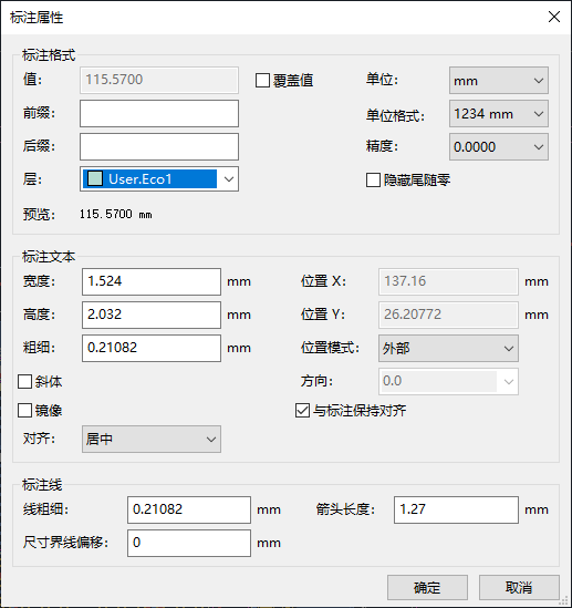
标注格式选项
覆盖值: 启用后,您可以直接在 值 字段中输入测量值,而不是实际测量值。
前缀: 此处输入的任何文字都将显示在测量值之前。
后缀: 此处输入的任何文字都将显示在测量值之后。
图层: 选择标注对象存在的层。
单位: 选择显示测量值的单位。 当更改电路板编辑器的显示单位时,自动 单位会导致标注单位发生变化。
单位格式: 从几种内置的单位显示风格中选择。
精度: 选择要显示多少位的精度。
标注文本选项
大多数标注文本选项与其他图形文本对象的选项相同(见上面的图形对象部分)。 也有一些特殊的选项适用于标注文本:
Position mode: Choose whether to position the dimension text manually, or to automatically keep it aligned with the dimension measurement lines.
与标注对齐: 开启后,标注文本的方向会自动调整,使文本与测量轴平行。
标注线选项
线条粗细: 设置构成标注形状的图形线的粗细。
标注界线偏移: 设置测量点到标注界线起点的距离。
箭头长度: 设置标注的形状的箭头段的长度。
引线选项
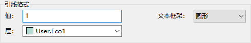
值: 输入要在引线行末尾显示的文本。
文本框架: 选择所需的文本周围的边界(圆形、矩形或无)。
布线
KiCad 具有交互式布线器的功能:
-
允许对单轨和差分对进行手动或拖动 (半自动) 布线。
-
可通过以下方式修改现有设计:
-
拖动现有布线时重新布线现有布线
-
拖动封装时重新布线连接到封装焊盘的布线
-
-
允许通过插入蛇形线 + 来调整布线长度和差分对的偏移(相位) 为具有严格时序要求的设计调整布线形状
默认情况下,布线器在放置布线时尊重配置的设计规则:新布线的尺寸(宽度)将取自设计规则,在确定新布线和过孔的放置位置时,布线器将尊重设计规则中设置的铜间隙。 如果需要的话,可以通过使用高亮冲突布线器模式和打开布线器设置中的允许 DRC 违规选项来禁用这种行为(见下文)。
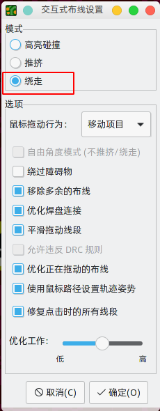
布线器有三种模式,可以随时选择。 布线器模式用于布线新布线,但也用于使用拖动(热键 D)命令拖动现有布线时。 这些模式是:
-
高亮冲突:在此模式下,大部分布线器功能被关闭,布线完全手动。 布线时,冲突 (间隙违规) 将以绿色高亮,如果存在冲突,则新布线的布线无法修复,除非打开了允许 DRC 冲突选项。 在此模式下,一次最多可以放置两个布线段 (例如,一个水平线段和一个对角线段)。
-
推挤:在此模式下,被布线的线段将绕过无法移动的障碍物 (例如,焊盘和锁定的布线/孔孔)和 推挤 障碍,这些障碍物可以移开。布线器在此模式下防止违反 DRC:如果无法布线到不违反 DRC 的光标位置,则不会创建新的布线。
-
绕走:在此模式下,布线器的行为与推挤模式相同,只是不会移动障碍物。
使用哪种模式是一个偏好问题。 对于大多数用户,我们建议使用推挤模式以获得最高效的布线体验,或者,如果您不希望布线器修改未被布线的线段,则建议使用绕走模式。请注意,推挤和绕走模式始终创建水平、垂直和 45 度 (H/V/45) 布线段。如果需要使用 H/V/45 以外的角度布线段,则必须使用高亮碰撞模式,并在交互布线器设置对话框中启用自由角度模式选项。
有五个主要的布线功能。单轨布线、差分对布线、调整单轨长度、调整差分对的长度和调整差分对的偏移 (相位)。 所有这些都存在于顶部工具栏上的路由菜单下拉菜单(单独)和绘图工具栏上的两个重载图标中,在右侧的绘图工具栏上。 上面介绍了重载图标的使用。 一个用于两个布线功能,一个用于三个调谐功能。 此外,布线菜单允许选择设置层对和交互式布线器设置。
要布线,请点击布线 ![]() 图标(从绘图工具栏或从顶部工具栏 布线 下)或使用热键 X。 点击一个起始位置,选择要布线的网络,并开始布线。 被布线的网络会自动高亮显示,网络的允许间隙会在被布线的线端周围用灰色的轮廓表示。 可以通过改变 "偏好设置" 对话框中的 "间隙轮廓" 设置来禁用间隙轮廓。
图标(从绘图工具栏或从顶部工具栏 布线 下)或使用热键 X。 点击一个起始位置,选择要布线的网络,并开始布线。 被布线的网络会自动高亮显示,网络的允许间隙会在被布线的线端周围用灰色的轮廓表示。 可以通过改变 "偏好设置" 对话框中的 "间隙轮廓" 设置来禁用间隙轮廓。
| 间隙轮廓显示从布线网络到 PCB 上任何其他铜线的最大间隙。 可以使用自定义设计规则为不同对象指定网络的不同间隙。 布线器将考虑这些间隙,但仅直观地显示最大间距值。 |
当布线器处于活动状态时,将从布线起点到编辑器光标绘制新的线段。这些线段是未固定临时 (unfixed temporary) 对象,它们显示当您使用左击或 Enter 键来固定布线 (fix the route) 时将创建哪些线段。非固定布线段以比固定布线段更亮的颜色显示。当您使用 Esc 键或通过选择另一个工具退出布线器时,将只保存固定布线段。完成布线操作(热键 End) 将固定所有布线并退出布线器。
在布线时,可以使用撤消最后一个布线段命令 (热键 Backspace) 取消固定最近固定的布线。您可以重复使用此命令以后退已固定的布线。
在以前的 KiCad 版本中,使用鼠标左键或 Enter 来固定已布线的线段会固定所有线段,但不包括鼠标光标位置结束的线段。 在 KiCad 6 中,这种行为现在是可选的,默认情况下,所有的线段 包括 在鼠标光标位置结束的线段都会被固定。 通过在交互式布线器设置对话框中禁用 "点击后固定所有线段" 选项,可以恢复旧的行为。
布线时,可以按住 Ctrl 键禁用网格捕捉,按住 Shift 键禁用对焊盘和过孔等对象的捕捉。
| 也可以通过更改首选项对话框的编辑选项部分中的磁吸点首选项来禁用对对象的捕捉。 我们建议您在一般情况下保持启用对象捕捉,这样就不会意外地在焊盘或过孔上略微偏离中心结束布线。 |
布线形态
在垂直(H) / 水平 (V) / 45 度模式下布线时,形态 是指一组两个线段如何连接单个 H/V/45 度线段无法到达的两个点。 在这种情况下,这些点将由一条水平或垂直线段和一条对角线 (45度) 线段连接。形态指的是这些线段的顺序:是水平/垂直线段还是对角线线段在前。

KiCad 的布线器试图根据一系列因素自动选择最佳形态。一般说来,布线器会尝试最大限度地减少路线中的拐角数量,并尽可能避免 "坏" 拐角 (如锐角)。当从焊盘布线或布线到焊盘时,KiCad 将选择将路线与焊盘最长边缘对齐的形态。
在某些情况下,KiCad 无法正确猜测您想要的形态。要在布线时切换布线的形态,请使用切换布线形态命令 (热键 /)。
在没有明显的“最佳”形态的情况下(例如,从过孔开始布线时),KiCad 将使用鼠标光标的移动来选择形态。如果希望布线从直线 (水平或垂直) 线段开始,请在水平或垂直方向上将鼠标从起始位置移开。如果您希望布线以对角线开始,请沿对角线方向移动。一旦光标与布线起始位置相距足够远,形态就会被锁定,并且除非光标回到起始位置,否则不会再更改。可以在交互式布线器设置对话框中禁用从鼠标光标移动检测形态,如下所述。
| 如果使用切换布线形态命令覆盖 KiCad 选择的形态,则在当前布线操作的其余部分中,将禁用从鼠标移动自动检测形体。 |
布线转角模式
当以 H/V/45 模式布线时,KiCad 的布线器可以放置尖角或圆角的布线。要在尖角和圆角之间切换,请使用布线拐角模式命令 (热键 Ctrl+/)。使用圆角布线时,每个布线步骤将放置直线段、单个圆弧或同时放置直线段和圆弧。布线形态决定首先放置圆弧还是直线段。
选择所需布线后,还可以在布线后使用圆角布线命令对布线拐角进行圆角处理。
| 尚不支持使用圆弧拖动布线。当拖动布线或在推挤模式下由布线器移动布线时,圆弧将转换回锐角。 |
布线宽度
被布线的线段的宽度是通过以下三种方式之一来确定的:如果布线的起点是现有线段的终点,并且顶部工具栏上的 ![]() 按钮被启用,宽度将被设置为现有布线的宽度。 否则,如果顶部工具栏中的布线宽度下拉菜单被设置为 "使用网络类宽度",则宽度将取自被布线的网络类(或任何为网络类指定不同宽度的自定义设计规则,例如在凹陷区域内)。 最后,如果布线宽度下拉菜单被设置为电路板设置对话框中配置的预定义布线尺寸之一,则将使用该宽度。
按钮被启用,宽度将被设置为现有布线的宽度。 否则,如果顶部工具栏中的布线宽度下拉菜单被设置为 "使用网络类宽度",则宽度将取自被布线的网络类(或任何为网络类指定不同宽度的自定义设计规则,例如在凹陷区域内)。 最后,如果布线宽度下拉菜单被设置为电路板设置对话框中配置的预定义布线尺寸之一,则将使用该宽度。
| 布线宽度永远不能低于在电路板设置对话框的约束部分中配置的最小布线宽度。如果添加的预定义宽度低于此最小约束,则将使用最小约束值。 |
KiCad 的布线器支持活动路线的单一布线宽度。 换句话说,要在线段中间改变宽度,你必须结束路线,然后从上一条线段的末端重新开始一条新的线段。 要改变活动线段的宽度,可使用热键 W 和 Shift+W,在电路板设置对话框中配置的布线宽度中逐步进行。
放置过孔
在布线线段时,切换层会在当前(未固定)线段的末端插入一个过孔。 一旦你放置了过孔,布线将继续在新层上进行。 有几种方法可以选择一个新层并插入过孔:
-
使用热键选择特定的图层,如 PgUp 选择
F.Cu或 PgDn 选择B.Cu。 -
通过使用 "下一层" 或 "上一层" 热键 (+ 和 -)。
-
通过使用 "放置过孔" 热键 (V),它将切换到活动层对中的下一层。
-
通过使用 "选择图层并通过通孔放置" 操作(热键 <),将打开一个对话框来选择目标层。
过孔的尺寸将从激活的过孔尺寸设置中获取,可通过顶部工具栏的下拉列表或增加过孔尺寸 (') 和减小过孔尺寸 (\) 热键访问。与布线宽度非常相似,当通孔大小设置为"使用网络类尺寸" 时,将使用 "电路板设置" 的 "网络类" 部分中配置的过孔大小 (除非被自定义设计规则覆盖)。
如果在电路板设置对话框的约束条件部分启用了微孔或盲/埋孔,就可以在布线时放置这些过孔。 使用热键 Ctrl+V 来放置微孔,Alt+Shift+V 来放置盲/埋孔。 微孔只能被放置在连接一个外铜层和相邻层的位置。 盲孔/埋孔可以放置在任何一层上。
布线器放置的过孔被认为是已布线线段的一部分。 这意味着过孔网络可以自动更新(就像线段网络一样),例如,当从原理图中更新 PCB 时改变了线段的网络名。 在某些情况下,这可能是不需要的,例如在创建邮戳孔时。 对于特定的过孔,可以通过关闭过孔属性对话框中的 "自动更新过孔网络" 复选框来禁用过孔网络的自动更新。 使用 "添加独立过孔" 工具放置的过孔在创建时禁用这一设置。
差分对布线
KiCad 中的差分对被定义为具有共同的 基数名称 和正负后缀的网路。 KiCad 支持使用 ` 和 `-`,或者 `P` 和 `N` 作为后缀。 例如,`USB 和 USB- 构成一对差分,USB_P 和 USB_N 也是如此。 在第一个例子中,基本名称是 USB,第二个例子中是 USB_。 后缀样式不能混合:网路 USB+ 和 USB_N 不构成差分对。 请确保你在原理图中相应地命名你的差分对网络,以便在 PCB 编辑器中使用差分对布线器。
要对差分对进行布线,请点击布线差分对 ![]() 图标(从绘图工具栏或从顶部工具栏 布线 下)或使用热键 6。 点击一个焊盘、过孔或现有差分对线段的末端,开始布线。 你可以从差分对的正网或负网开始布线。
图标(从绘图工具栏或从顶部工具栏 布线 下)或使用热键 6。 点击一个焊盘、过孔或现有差分对线段的末端,开始布线。 你可以从差分对的正网或负网开始布线。
| 目前不可能在现有差分对布线的中间开始对差分对进行布线。 |
差分对布线器将尝试用设计规则中的间隙布线这对布线(差分对间隙可以在电路板设置对话框的网络类部分中配置,也可以通过使用自定义设计规则来配置)。如果布线的起始或结束位置与配置的间隙不同,布线器将创建一个较短的 "扇出" 部分,以最大限度地缩短差分对未耦合的布线长度。
当交换层或使用放置过孔 (V) 操作时,差分对布线器将创建两个相邻的过孔。这些过孔将被放置在尽可能靠近彼此的位置,同时遵守铜和孔到孔间隙的设计规则。
修改布线
线段被布线后,可以通过移动或拖动来修改它们,或者删除并重新布线。 当选择一个线段时,热键 U 可以用来将选择范围扩大到所有连接的线段。 第一次按下 U 将选择与焊盘或过孔最近的连接点之间的线段。 第二次按 U 将再次扩大选择范围,包括所有层上与所选线段相连的所有线段。 用这种技术选择线段可以用来快速删除整个布线网络。
有两种不同的拖动命令可用于修改布线段。拖动 (45 度模式) 命令热键 D 用于通过布线器拖动布线。如果布线器模式设置为推挤,则使用此命令拖动将推挤附近的布线。如果布线器模式设置为绕走,则使用此命令拖动将绕过障碍物或停在障碍物处。拖动自由角度命令 热键 G 用于将布线段一分为二,并将新角点拖动到任何位置。拖动自由角度的行为类似于高亮碰撞布线器模式:不会避开或推挤障碍物,只会高亮。
| 目前还不能拖动包含圆弧的布线。在某些情况下,尝试拖动这些布线会导致圆弧被删除。可以通过选中特定圆弧并使用拖动命令 (D) 来调整其大小。使用此命令调整圆弧大小时,不执行 DRC 检查。 |
移动命令(热键 M)也可以在线段上使用。 该命令将拾取选定的线段,而忽略任何未被选中的附加线段或过孔。 使用移动命令移动线段时,不会进行 DRC 检查。
在移动封装的同时,可以对附着在封装上的线段进行重新布线。 要做到这一点,在选择了一个封装的情况下使用拖动命令(D)。 任何以封装的一个焊盘为终点的线段都将与封装一起被拖动。 这个功能有一些限制:它只在高亮冲突模式下运行,所以附着在封装上的线段不会绕过障碍物或将附近的线段推开。 此外,只有以封装的焊盘为终点的线段才会被拖动。 仅仅穿过焊盘或在原点以外的焊盘上结束的线段将不会被拖动。
可以使用编辑布线和过孔对话框修改布线的宽度和过孔的大小,而无需重新布线。有关详细信息,请参阅下面关于批量编辑工具的部分。
长度调整
长度调谐工具可用于在布线后为线段添加蛇形调谐形状。 要调整线段的长度,首先要挑选合适的长度调谐工具。 单线调谐工具(图标 ![]() 或热键 7)将添加蛇形图形,使单线的长度达到目标值。 差分对调谐工具(图标
或热键 7)将添加蛇形图形,使单线的长度达到目标值。 差分对调谐工具(图标 ![]() 或热键 8)将为差分对做同样的事情。 差分对偏斜调整工具(图标
或热键 8)将为差分对做同样的事情。 差分对偏斜调整工具(图标 ![]() 或热键 9)将为差分对中较短的成员增加长度,以消除差分对正负两边的偏斜(相位差)。 与 "布线" 图标一样,"调谐" 图标可以在顶部工具栏的 "布线" 菜单下拉框和右侧的绘图工具栏中找到。
或热键 9)将为差分对中较短的成员增加长度,以消除差分对正负两边的偏斜(相位差)。 与 "布线" 图标一样,"调谐" 图标可以在顶部工具栏的 "布线" 菜单下拉框和右侧的绘图工具栏中找到。
要选择长度调整工具的目标长度,请在激活长度调整工具后,从上下文菜单或使用热键 Ctrl+L 打开 "长度调整设置" 对话框:
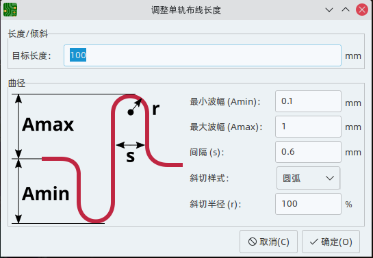
此对话框还可用于配置曲折形状的大小、形状和间距。
配置好目标长度后,在你希望开始放置蛇形形状的区域点击一个布线。 沿着线段移动鼠标光标,蛇形形状就会被添加。 光标旁边会出现一个状态窗口,显示布线的当前长度和目标长度。 再次点击,完成放置当前的蛇形布线。 如果需要,可以在同一条布线上放置多条蛇形布线。
| 长度调整工具仅支持调整两个焊盘之间的点对点网络的长度。尚不支持调整具有不同拓扑的网络长度。 |
交互式布线设置
交互式布线器设置可通过路径菜单访问,或通过右键单击工具栏中的布线按钮来访问。这些设置控制布线和拖动现有布线时的布线行为。
| 设置 | 说明 |
|---|---|
模式 |
设置用于创建新布线和拖动现有布线的路由器的操作模式。 有关详细信息,请参阅上面的内容。 |
自由角度模式 |
允许以任何角度布线,而不是仅以 45 度增量布线。 仅当布线模式设置为突出显示高亮冲突时, 此选项才可用。 |
绕过障碍物 |
在推挤模式下,允许布线尝试在实心障碍物 (如焊盘) 后面移动碰撞布线。 |
移除多余的布线 |
自动删除在当前布线中创建的回路, 仅保留回路中最近布线的部分。 |
优化焊盘连接 |
启用此设置时,交互式布线器尝试在退出焊盘和过孔时避免锐角 和其他不需要的布线。 |
平滑拖动线段 |
拖动布线时,会尝试将布线段组合在一起, 以最大限度地减少方向更改。 |
允许违反 DRC 规则 |
在高亮碰撞模式下,允许放置违反 DRC 规则的布线和过孔。 在其他模式下不起作用。 |
优化正在拖动的布线 |
启用后,拖动布线段将导致 KiCad 优化屏幕上可见的其余布线。 优化过程去除了不必要的拐角,避免了锐角,通常会尝试找到布线的最短路径。 禁用时,不会对正在拖动的紧邻部分之外的布线执行任何优化。 在拖动布线时尝试优化布线。 |
使用鼠标路径设置布线形态 |
尝试根据鼠标路径从布线起点位置拾取布线形态。 如果鼠标从开始位置开始主要沿对角线移动,则形态将设置为对角线起点; 如果鼠标主要水平或垂直移动,则形态将设置为垂直起点。 当鼠标离开布线起始位置很远时,形态估计就会被锁定, 并且可以通过移回起始位置来解锁。 |
点击时固定所有线段 |
启用时,在布线时单击将固定已布线的所有布线段的位置, 包括在鼠标光标结束的线段。新的线段将从鼠标光标位置开始。 禁用时,最后一个线段 (在鼠标光标处结束的线段) 将不会固定在适当位置, 可以通过进一步的鼠标移动进行调整。 |
向前和向后批注
| TODO:写下这一节 |
位置重新批注
| TODO:写下这一节 |
锁定
大多数对象可以通过其属性对话框、右键上下文菜单或使用 "切换锁定" 热键(L)来锁定。 被锁定的对象不能被选择,除非选择过滤器中的 "被锁定的项目" 复选框被启用。 试图移动锁定的项目将导致一个警告对话框:
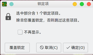
在这个对话框中选择 "覆盖锁定" 将允许移动锁定的项目。 选择 "确定" 将允许你在选择中移动任何未上锁的项目;留下锁定的项目。 选择 "不再显示" 将使你在剩下的会话中记住你的选择。
批量编辑工具
| TODO:写下这一节 |
清理工具
| TODO:写下这一节 |
正在导入图形
| TODO:写下这一节 |
从 DXF 和 SVG 文件导入矢量图
| TODO:写下这一节 |
正在导入位图图像
| TODO:写下这一节 |
检查电路板
测量工具
测量工具允许你在 PCB 上的各点之间进行距离和角度测量。 要激活该工具,请点击右侧工具栏的 ![]() 图标,或使用热键 Ctrl+Shift+M。 一旦该工具被激活,点击一次以设置测量起点,然后再点击一次以完成测量。
图标,或使用热键 Ctrl+Shift+M。 一旦该工具被激活,点击一次以设置测量起点,然后再点击一次以完成测量。
| 测量工具用于不需要永久显示的快速测量。 您所做的任何测量都将仅在该工具处于活动状态时显示。 要创建将显示在打印输出和打印中的永久性尺寸标注,请使用尺寸标注工具。 |
设计规则检查
设计规则检查器用于验证 PCB 是否符合电路板设置对话框中建立的所有要求,以及所有焊盘是否按照网表或原理图连接。 KiCad 可以在布线线段时自动防止一些违反设计规则的行为,但许多其他的行为是无法自动防止的。 这意味着在为 PCB 创建制造文件之前,必须使用设计规则检查器。
要使用设计规则检查器,请点击顶部工具栏的 ![]() 图标,或者从检查菜单中选择设计规则检查器。
图标,或者从检查菜单中选择设计规则检查器。
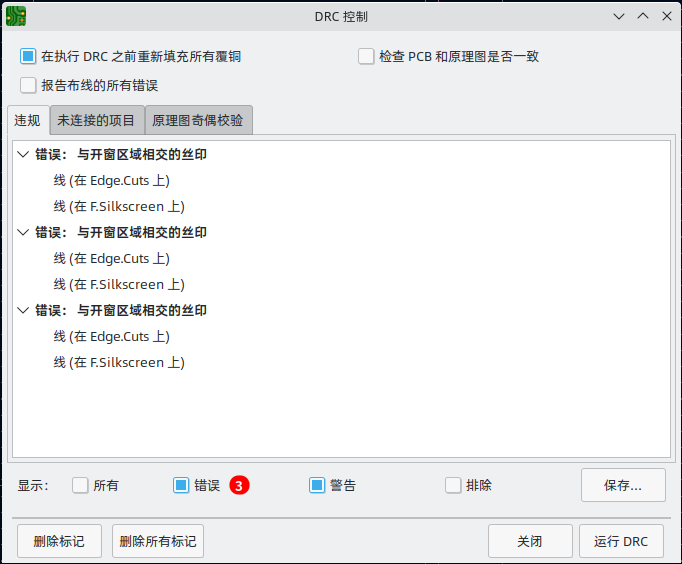
DRC 控制窗口的顶部部分包含一些控制设计规则检查器的选项:
重新填充所有敷铜后再执行 DRC: 启用后,每次运行设计规则检查器时都会重新填充敷铜。 如果未手动重新填充敷铜,禁用此选项可能会导致错误的 DRC 结果。
报告每个布线的所有错误: 启用后,将报告每个线段的所有间隙错误。 禁用时,将只报告第一个错误。 启用此选项将导致设计规则检查器运行速度变慢。
测试 PCB 和原理图之间的奇偶校验: 启用后,设计规则检查器除了测试 PCB 设计规则外,还将测试原理图和 PCB 之间的差异。 在独立模式下运行 PCB 编辑器时,该选项不起作用。
运行 DRC 后,任何违规行为都会显示在 DRC 控制窗口的中间部分。 违反规则、未连接的项目以及原理图和 PCB 之间的差异会显示在三个不同的标签中。 违规列表下面的控件可以用来显示或隐藏违规,这取决于其严重程度。 在运行 DRC 后,可以使用保存按钮创建一个纯文本格式的报告文件。
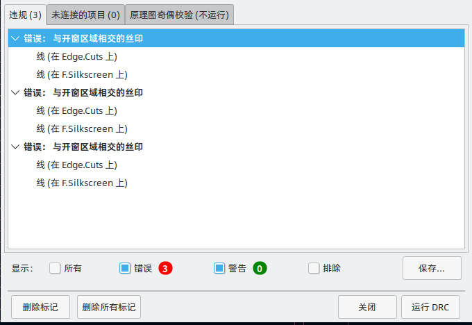
每项违规行为涉及 PCB 上的一个或多个对象。 在违章列表中,涉及的对象列在违章下面。 点击列表中的违规行为将移动 PCB 编辑器的视图,使受影响的区域居中。 点击违章所涉及的对象之一将突出显示该对象。
右键单击列表视图中的违规行为将打开一个上下文菜单,其中包括排除所选违规行为的额外操作。 除非 DRC 控制窗口底部的 "排除" 复选框被激活,否则排除的违反行为会被隐藏。 被排除的违规行为在设计规则检查器运行期间会被记住。
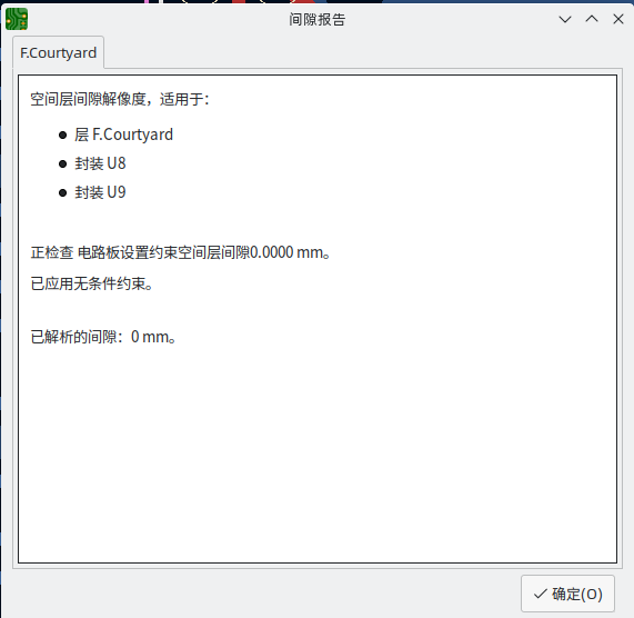
间隙和约束解析
间隙和约束解决工具允许你检查哪些间隙和设计约束规则适用于选定的项目。 当设计具有复杂设计规则的 PCB 时,这些工具可以提供帮助,因为在这种情况下并不总是清楚哪些规则适用于某个对象。
要检查两个对象之间适用的间隙规则,选择这两个对象并从检查菜单中选择间隙分辨率。 间隙报告对话框将显示每个铜层上的对象之间所需的间隙,以及产生该间隙的设计规则。
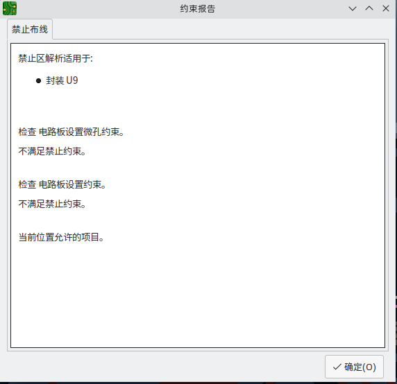
To inspect the design constraints that apply to an object, select it and choose Constraints Resolution from the Inspect menu. The Constraints Report dialog will show any constraints that apply to the object.
Find tool
The Find tool searches for text in the PCB, including reference designators, footprint fields, and graphic text. When the tool finds a match, the canvas is zoomed and centered on the match and the text is highlighted. Launch the tool using the (![]() ) button in the top toolbar.
) button in the top toolbar.
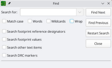
The Find tool has several options:
Match case: Selects whether the search is case-sensitive.
Words: When selected, the search will only match the search term with complete words in the PCB. When unselected, the search will match if the search term is part of a larger word in the PCB.
Wildcards: When selected, wildcards can be used in the search terms. ?
matches any single character, and * matches any number of characters. Note
that when this option is selected, partial matches are not returned: searching
for abc* will match the string abcd, but searching for abc will not.
Wrap: When selected, search results will return to the first hit after reaching the last hit.
Search footprint reference designators: Selects whether the search should apply to footprint reference designators.
Search footprint values: Selects whether the search should apply to footprint value fields.
Search other text items: Selects whether the search should apply to other text items, including graphical text and footprint fields other than value and reference.
Search DRC markers: Selects whether the search should apply to the violation descriptions of DRC markers shown on the board.
3D 查看器
The 3D Viewer shows a 3-dimensional view of the board and the components on the board. You can view the board from different perspectives, show or hide different types of components, cross-probe from the PCB Editor to the 3D viewer, and generate raytraced renders of the board.
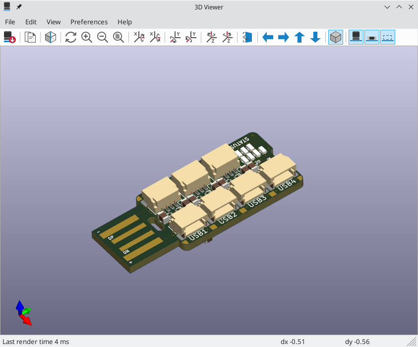
| The 3D model for a component will only appear if the 3D model file exists and has been assigned to the footprint. |
| Many footprints in KiCad’s standard library do not yet have model files created for them. However, these footprints may contain a path to a 3D model that does not yet exist, in anticipation of the 3D model being created in the future. |
Navigating the 3D view
Dragging with the left mouse button will orbit the 3D view around the centroid of the board. Scrolling the mouse wheel will zoom the view in or out. Scrolling while holding Ctrl pans the view left and right, and scrolling while holding Shift pans up and down. Dragging with the middle mouse button also pans the view.
Different sized 3D grids can be set using the Preferences → 3D Grid menu. Bounding boxes for each component can be enabled with Preferences → Show Model Bounding Boxes.
When the PCB Editor and the 3D Viewer are both open, selecting a footprint in the PCB Editor will also highlight the component in the 3D Viewer. The highlight color is adjustable in Preferences → Preferences… → 3D Viewer → Realtime Renderer → Selection Color.
Generating images with the 3D Viewer
The current 3D view can be saved to an image with File → Export Current View as PNG… or Export Current View as JPG…, depending on the desired image format. The current view can also be copied to the clipboard using the ![]() button, or Edit → Copy 3D Image.
button, or Edit → Copy 3D Image.
The 3D Viewer has a raytracing rendering mode which displays the board using a more physically accurate rendering model than the default rendering mode. Raytracing is slower than the default rendering mode, but it can be used when the most visually attractive results are desired. Raytracing mode is enabled with the ![]() button, or with Preferences → Raytracing. The 3D grid and selection highlights are not shown in raytracing mode.
button, or with Preferences → Raytracing. The 3D grid and selection highlights are not shown in raytracing mode.
Colors and other rendering options, for both raytraced and non-raytraced modes, can be adjusted in Preferences → Preferences… → 3D Viewer.
3D viewer controls
Many viewing options are controlled with the top toolbar.
|
Reload the 3D model |
|
Copy 3D image to clipboard |
|
Render current view using raytracing |
|
Zoom in |
|
Zoom out |
|
Redraw |
|
Fit drawing in display area |
|
Rotate X clockwise |
|
Rotate X counterclockwise |
|
Rotate Y clockwise |
|
Rotate Y counterclockwise |
|
Rotate Z clockwise |
|
Rotate Z counterclockwise |
|
Flip board view |
|
Pan board left |
|
Pan board right |
|
Pan board up |
|
Pan board down |
|
Enable/disable orthographic projection |
|
Show/hide 3D models for through-hole components |
|
Show/hide 3D models for surface mount components |
|
Show/hide 3D models for components of type 'other' |
网络检查
网络检查器允许你查看电路板中所有网络的统计数据。 要打开检查器,请点击外观面板中的网络部分顶部的 ![]() 图标,或者从检查菜单中选择网络检查器。
图标,或者从检查菜单中选择网络检查器。
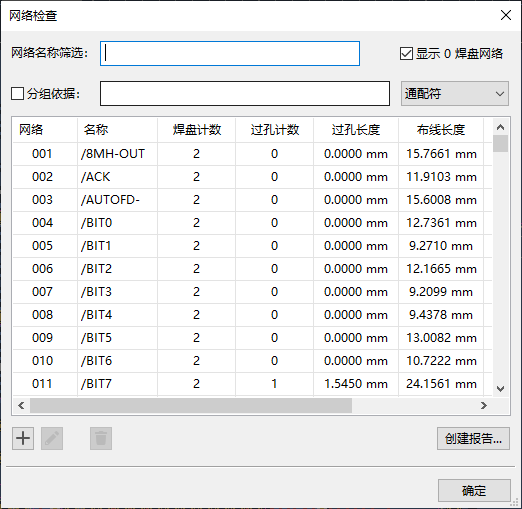
点击网络列表中的一个网络会在电路板上高亮显示该网络。 单击列标题允许您按该列对网络列表进行排序。
分组依据字段允许您将不同的网络组合在一起,并查看组合的网络的总长度。 例如,如果您有两个名为 DATA0 和 DATA0_EXT 的网络,则使用值为 DATA0* 的分组依据将创建一个包含这两个网络的组。 通过将分组依据模式从通配符更改为 RegEx (正则表达式),可以创建更复杂的分组。 分组依据模式的子字符串 (Substr) 变体将为以不同方式匹配该模式的每组网络创建组。
例如,如果您有 U1D+,U1D-,U2D+ 和 U2D-,分组模式 U*D 将在通配符模式下匹配所有四个网络,创建一个单一的组 U*D。 在通配符子串模式下,它将匹配所有四个网络,但创建两个不同的组:U1D 和 U2D。
Pad Count and Via Count show the number of pads (surface mount and through hole) and vias on a net. Via Length shows the total height of each via (not accounting for which copper layers the via connects to). In other words, Via Length is equal to Via Count multiplied by the stackup height of the board. Track Length shows the total length of all track segments in a net, not accounting for topology. Die length shows the total of all Pad to Die Length values set for pads on the net.
| 网络检查器中显示的长度不同于长度调整工具中显示的长度, 因为网络检查器显示连接到网络的所有布线的总和, 而长度调整工具显示最近的两个焊盘或分支过孔之间的距离。 有关长度调整工具的更多信息,请参见布线部分。 |
生成输出
KiCad 可以生成和导出多种不同格式的文件,对制造 PCB 和与外部软件的接口很有用。 该功能可在文件菜单的几个不同部分中找到。 制造输出部分包含准备制造 PCB 所需的最常见操作。 输出部分包含生成可由外部软件读取的文件的工具。 绘图功能允许你以各种格式导出 PCB 的 2D 线图。 打印功能允许你将 PCB 的视图发送到 2D 打印机上。
制造输出和绘制
KiCad 使用 Gerber 文件作为其 PCB 制造的主要绘图格式。 要创建 Gerber 文件,请从文件菜单中打开绘图对话框,或从文件菜单的制造输出部分选择 Gerbers。 绘图对话框将打开,允许你配置和生成 Gerber 文件。
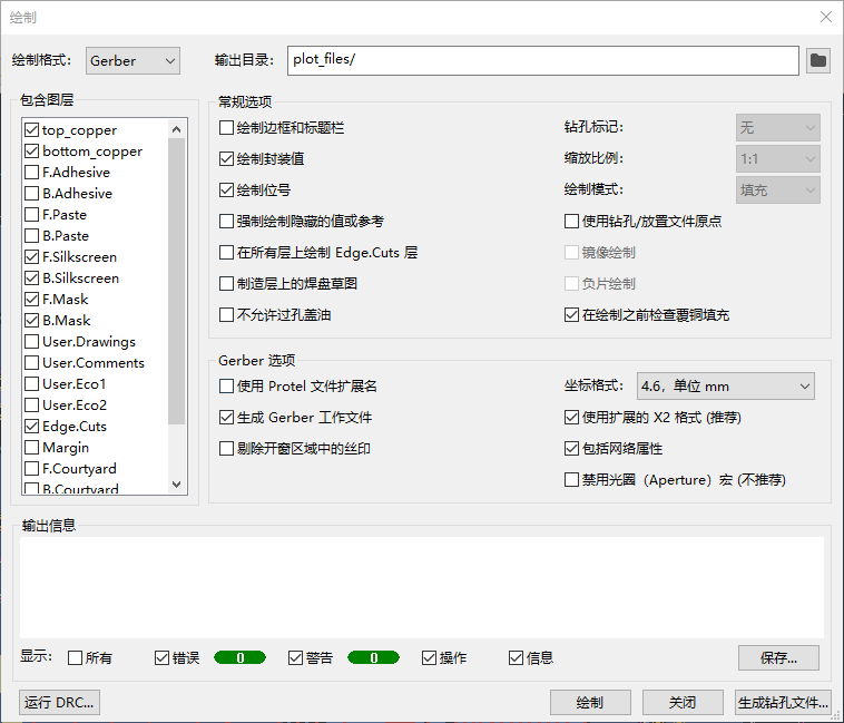
绘制选项
包含层: 检查列表中是否启用了您的电路板上使用的每一层。 将不打印禁用的图层。
输出目录: 指定打印文件的保存位置。 如果这是相对路径,则它是相对于工程目录创建的。
打印边框和标题栏: 如果启用,将在每个图层上打印图纸边框和标题栏。 打印 Gerber 文件时,通常应禁用此功能。
绘制封装值: 如果启用,每个封装的值字段将绘制在其所在的任何层上 (除非特定封装的字段可见性被禁用)。
绘制位号: 如果启用,每个封装的位号字段将绘制在其所在的任何层上 (除非特定封装的字段可见性被禁用)。
强制绘制不可见值/位号: 如果启用,将绘制所有封装值和位号,即使其中一些字段禁用了字段可见性。
在所有图层上绘制 Edge.Cuts: 如果启用,Edge.Cuts(电路板轮廓) 图层将添加到所有其他层。 请向您的制造商咨询,了解此设置对于其制造过程的正确值是多少。
制造层上的草图焊盘: 如果启用,制造 (F.Fab,B.Fab) 层上的封装焊盘将绘制为未填充的轮廓,而不是填充的形状。
请勿覆盖过孔: 如果启用,过孔将不会覆盖在阻焊层 (F.Mask、B.Mask) 上。 如果禁用,过孔将由阻焊层 (绿油) 覆盖。
| KiCad 不支持覆盖或开窗特定过孔。 覆盖只能是全局控制的(一块板上的所有过孔)。 |
钻孔标记: 对于 Gerber 以外的绘图格式,可以在所有钻孔的位置绘制标记。 钻孔标记可以按成品孔的实际尺寸 (直径) 上创建,也可以在更小的尺寸上创建。
缩放: 对于支持非 1:1 缩放的打印格式,可以设置打印比例。 自动缩放设置将缩放绘图以适合指定的页面大小。
绘制模式: 对于某些绘制格式,填充的形状可能只被绘制成轮廓(草图模式)。
使用钻孔/放置文件原点: 启用后,绘制文件的坐标原点将是电路板编辑器中设置的钻孔/放置文件原点。 禁用时,坐标原点将是绝对原点 (图框的左上角)。
镜像绘制: 当设置该选项时,对于某些绘制格式,可能会水平镜像输出。
负片绘制: 对于某些绘制格式,可能会将输出设置为负片模式。 在此模式下,将为电路板轮廓内的空白区域绘制图形,并在 PCB 中存在对象的位置留下空白区域。
绘制前检查敷铜填充: 启用后,将在生成输出之前检查敷铜填充 (如果过期则重新填充)。 如果禁用此选项,绘制输出可能不正确!
Gerber 选项
使用 Protel 文件扩展名: 启用后,绘制的 Gerber 文件将使用基于 Protel (.GBL、.GTL 等) 的文件扩展名命名。
当禁用时,文件将有 .gbr 的扩展名。
生成 Gerber 作业文件: 开启后,Gerber 作业文件 (.gbrjob) 将与任何 Gerber 文件一起生成。
Gerber 作业文件是 Gerber 格式的扩展,包括有关 PCB 压层、材料和表面处理的信息。
有关 Gerber 工作文件的更多信息,请访问链接:https://www.ucamco.com/en/gerber/gerber-job-file[Ucamco 网站]。
坐标格式: 配置坐标在绘制的 Gerber 文件中的存储方式。 请咨询您的制造商,了解他们对此选项的推荐设置。
使用扩展 X2 格式: 启用后,绘制的 Gerber 文件将使用 X2 格式,其中包括有关网表和其他扩展属性的信息。 此格式可能与某些制造商使用的旧版 CAM 软件不兼容。
包含网表属性: 启用后,绘制的 Gerber 文件将包含可用于在 CAM 软件中检查设计的网表信息。 禁用 X2 格式模式时,此信息将作为注释包含在 Gerber 文件中。
禁用光圈宏: 启用后,所有形状将作为基元绘制,而不是使用光圈宏。 此设置仅在制造商要求时用于与旧的或有错误的 CAM 软件兼容。
Postscript 选项
Scale factor: Controls how coordinates in the board file will be scaled to coordinates in the PostScript file. Using a different value for X and Y scale factors will result in a stretched / distorted output. These factors may be used to correct for scaling in the PostScript output device to achieve an exact-scale output.
Track width correction: A global factor that is added (or subtracted, if negative) from the size of tracks, vias, and pads when plotting a PostScript file. This factor may be used to correct for errors in the PostScript output device to achieve an exact-scale output.
强制 A4 输出: 启用后,生成的 PostScript 文件将为 A4 大小,即使 KiCad 电路板文件大小不同。
SVG 选项
单位: 控制 SVG 文件中使用的单位。 由于 SVG 格式没有指定的单位系统, 因此您必须使用与导入到其他软件时要使用的单位设置相同的单位设置进行导出。
精度: 控制将使用多少个有效数字来存储坐标。
DXF 选项
使用图形项目的轮廓绘制图形项目: DXF 文件中的图形形状没有宽度。 此选项控制如何将 KiCad 电路板中具有宽度 (厚度) 的图形图形绘制到 DXF 文件。 启用此选项后,将绘制形状的外轮廓。 禁用此选项时,将打印形状的中心线 (并且形状的厚度在生成的 DXF 文件中不可见)。
使用 KiCad 字体绘制文本: 启用后,KiCad 设计中的文本将使用 KiCad 字体绘制为图形形状。 禁用时,文本将作为 DXF 文本对象绘制,它将使用不同的字体,并且不会以与 KiCad 电路板编辑器中显示的完全相同的位置和大小显示。
导出单位: 控制将在 DXF 文件中使用的单位。 由于 DXF 格式没有指定的单位系统,因此您必须使用与导入到其他软件时要使用的单位设置相同的单位设置进行导出。
HPGL 选项
默认笔尺寸: 控制用于创建图形的绘图仪笔尺寸。
钻孔文件
KiCad 可以生成大多数 PCB 制造工艺所需的 Excellon 或 Gerber X2 格式的数控钻孔文件。 KiCad 还可以生成钻孔图:一个显示钻孔位置的电路板图形图。 从 "制造输出" 菜单中选择 "生成钻孔文件" 选项来打开该对话框:
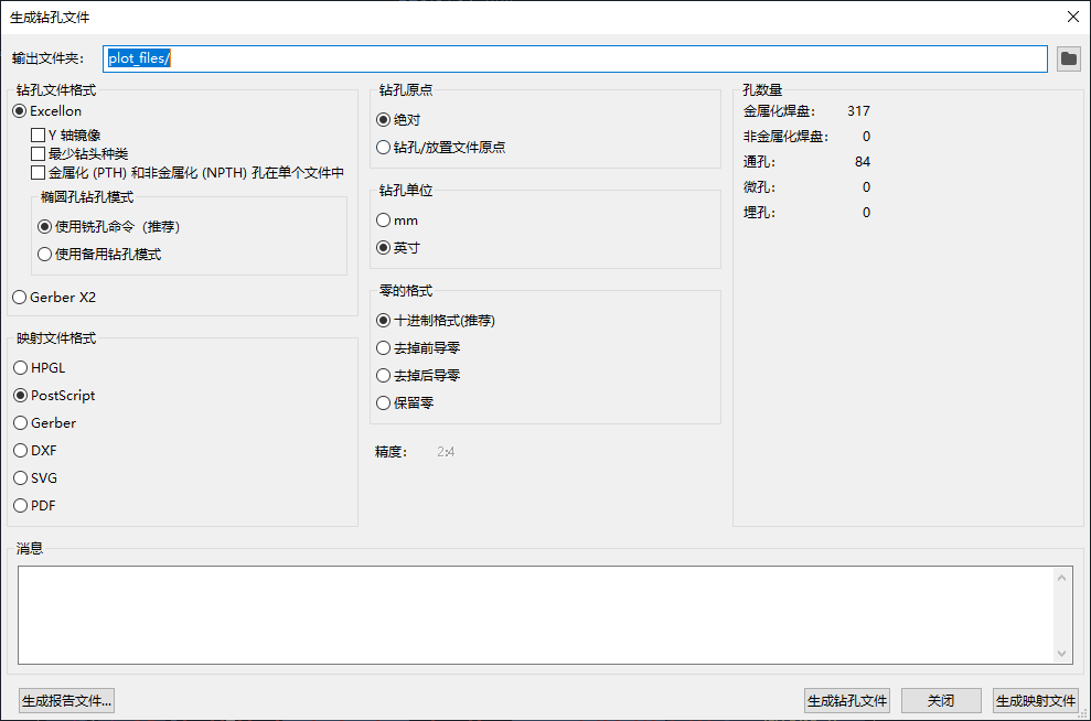
输出文件夹: 选择要保存生成的钻孔和映射文件的文件夹。 如果输入相对路径,则它将相对于工程目录。
钻孔文件格式: 选择是生成 Excellon 钻孔文件 (大多数 PCB 制造商都需要)还是 Gerber X2 文件。
镜像 Y 轴: 对于卓越文件,选择是否镜像 Y 轴坐标。 当由第三方制造 PCB 时,通常不应使用该选项,并且是为了方便自己制造 PCB 的用户而提供的。
最小钻头: 对于 Excellon 文件,选择是否输出最小钻头,而不是完整的文件钻头。 除非制造商要求,否则不应启用此选项。
PTH (电镀孔) 和 NPTH (非电镀孔) 为单文件: 默认情况下,会在两个不同的 Excellon 文件中生成电镀孔和非电镀孔。 启用此选项后,这两个文件将合并为单个文件。 除非制造商要求,否则不应启用此选项。
椭圆孔钻孔模式: 控制椭圆孔在 Excellon 钻孔文件中的表示方式。 默认设置 使用布线命令 对于大多数制造商都是正确的。 如果制造商要求,请仅选择 使用备用钻孔模式 设置。
映射文件格式: 选择绘制钻孔映射的输出格式。
钻孔原点: 选择钻孔文件的坐标原点。 绝对 将使用左上角的页面原点。 钻孔/放置文件原点 将使用电路板设计中指定的原点。
钻孔单位: 选择钻孔坐标和尺寸的单位。
零的格式 控制 Excellon 钻孔文件中数字的格式。 请根据制造商的建议在此处选择一个选项。
元件放置文件
元件放置文件是一种文本文件,它列出了电路板上的每个元件(封装)以及其中心位置和方向。 这些文件通常用于对取放机进行编程,如果你订购的是完全组装的 PCB,你的制造商可能需要这些文件。
| 如果为生成的封装启用了“从放置文件中排除”选项,该封装将不会出现在生成的放置文件中。 这可用于排除不代表要组装的物理元件的某些封装。 |
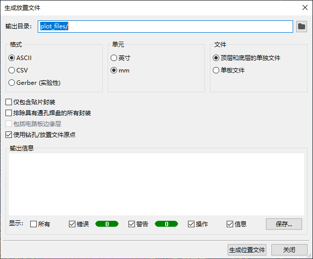
格式: 选择生成纯文本 (ASCII)、逗号分隔文本 (CSV) 或 Gerber 放置文件格式。
单位: 在放置文件中选择元件位置的单位。
文件: 选择是为电路板正面和背面的封装生成单独的文件,还是生成一个合并两面的文件。
Include only SMD footprints: When enabled, only footprints with the SMD fabrication attribute will be included. Check with your manufacturer to determine if non-SMD footprints should be included or excluded from the position file.
使用通孔焊盘排除所有封装: 启用时,如果封装包含任何通孔焊盘,即使其制造类型设置为 SMD,也将从放置文件中排除封装。
包括电路板边缘层: 对于 Gerber 放置文件,控制电路板轮廓是否包含在封装放置数据中。
使用钻孔/放置文件原点: 启用后,元件位置将相对于电路板设计中设置的钻孔/放置文件原点。 禁用时,位置将相对于页面原点 (左上角)。
额外的制造产出
KiCad 还可以从电路板设计生成封装报告文件、IPC-D-356 网表文件和物料清单 (BOM)。 这些输出格式没有可配置的选项。
打印
KiCad 可以使用文件菜单中的打印操作将电路板视图打印到标准打印机上。
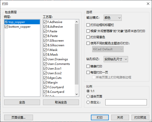
包含层: 选择要包含在打印输出中的层。未选中的层将不可见。
输出模式: 选择以黑白或全彩方式打印。
打印边框和标题块: 启用后,将打印页面边框和标题块。
根据外观管理器的对象选项卡打印: 启用后,任何隐藏在外观面板的对象选项卡中的对象都将隐藏在打印输出中。 禁用时,如果在包含的图层区域中选择了这些对象所在的图层,则将打印这些对象。
打印背景色: 全彩色打印时,该选项控制是否打印视图背景色。
使用不同的颜色主题进行打印: 当以全色打印时,此选项允许使用不同的颜色主题进行打印。 禁用时,电路板编辑器使用的颜色主题将用于打印。
钻孔标记: 控制是以实际大小显示钻孔,还是以较小的尺寸显示钻孔,还是将其隐藏在打印输出中。
打印镜像: 启用后,打印输出将被水平镜像。
每层打印一页: 启用后,在包含图层区域中选择的每一图层都将打印到单独一页。 如果启用此选项,在所有页面上打印电路板边缘 选项控制是否将 Edge.Cuts 层添加到每个打印页面。
比例: 控制打印输出相对于页面设置中配置的页面大小的比例。
正在导出文件
KiCad 可以将电路板设计导出为各种第三方格式,以便与外部软件一起使用。 这些功能可以在文件菜单的导出部分找到。
Specctra .DSN: 创建适合导入到某些第三方自动布线软件中的文件。 此导出器没有可配置的选项。
| TODO:文档 GenCAD 导出器 |
| TODO: 文档 VRML 导出器 |
IDF Exporter
The IDF exporter exports an IDFv3 compliant board (.emn) and library (.emp) file for communicating mechanical dimensions to a mechanical CAD package. The exporter exports the board outline and cutouts, all pad and mounting through holes including slotted holes, and component outlines; this is the most basic set of mechanical data required for interaction with mechanical designers. All other entities described in the IDFv3 specification are currently not exported.
| You must attach IDF component models to your design’s footprints before they will be included in the exported model. For more information on attaching models to footprints, see the footprint documentation. Some IDF-specific guidance is included in the Advanced Topics documentation. |
| For more information on creating IDF component models, including descriptions of the IDF utility tools included with KiCad, see the Advanced Topics documentation. |
Once models have been specified for all desired components, the model of the board can be exported. In the PCB Editor, select File → Export → IDFv3….
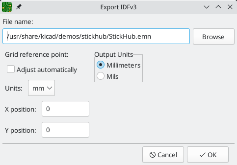
Grid reference point: Choose where the exported model’s reference point should be. If the Adjust automatically option is selected, KiCad will set the reference point to the centroid of the PCB. Otherwise, the reference point is set relative to the display origin.
Output units: Choose whether the exported model’s units are millimeters or mils.
The outputs can be viewed directly in a mechanical CAD application or converted to VRML using the idf2vrml tool.
| TODO: 文档 STEP 导出器 |
| TODO: 文档 SVG 导出器 |
| TODO: 文档 CMP 文件导出器 |
Hyperlynx: 创建适合导入 Mentor Graphics(Siemens) HyperLynx 模拟和分析软件的文件。
封装和封装库
管理封装库
KiCad’s footprint library management system allows directly using several types of footprint libraries:
-
KiCad
.prettyfootprint libraries (folders with .pretty extension, containing .kicad_mod files) -
KiCad Legacy footprint libraries (.mod files)
-
GEDA libraries (folders containing .fp files)
-
Eagle footprint libraries
KiCad only supports writing to KiCad’s native .pretty format footprint libraries (and the .kicad_mod footprint files within them). All other footprint library formats are read-only.
|
KiCad uses a table of footprint libraries to map footprint libraries of any supported library type to a library nickname. KiCad uses a global footprint library table as well as a table specific to each project. To edit either footprint library table, use Preferences → Manage Footprint Libraries….
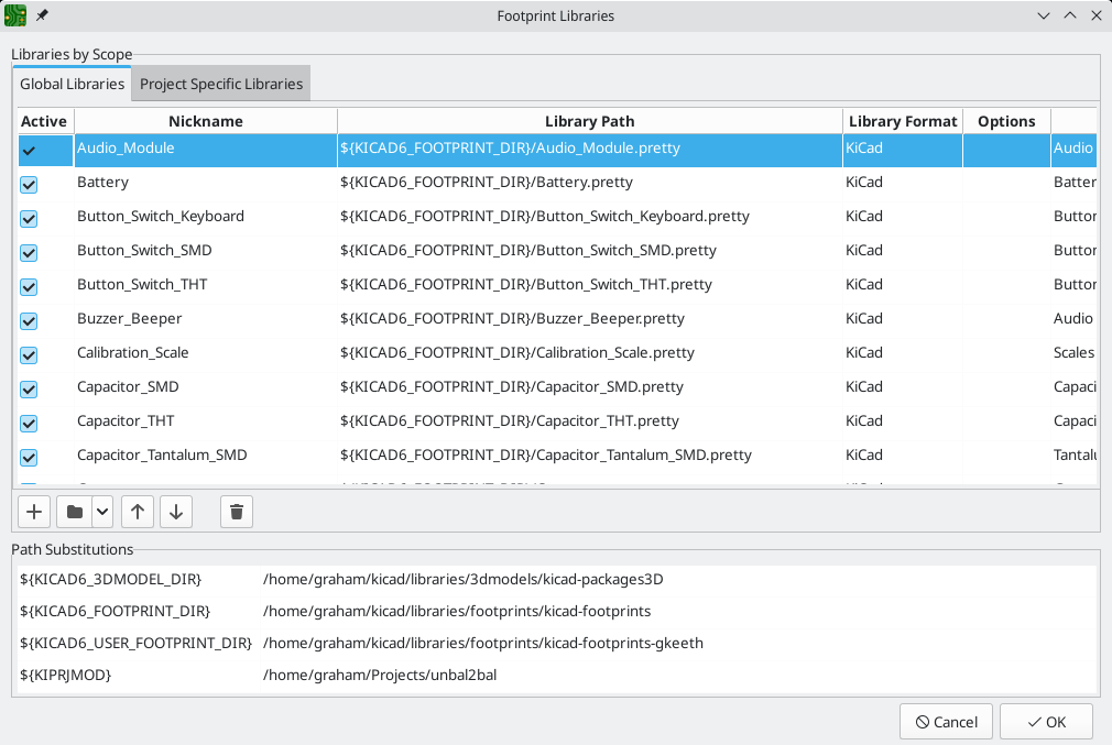
The global footprint library table contains the list of libraries that are always available regardless of the currently loaded project. The table is saved in the file fp-lib-table in the KiCad configuration folder. The location of this folder depends on the operating system being used.
The project specific footprint library table contains the list of libraries that are available specifically for the currently loaded project. If there are any project-specific footprint libraries, the table is saved in the file fp-lib-table in the project folder.
Initial Configuration
The first time the PCB Editor (or any other KiCad tool that uses footprints) runs and the global footprint table file fp-lib-table is not found, KiCad will guide the user through setting up a new footprint library table. This process is described above.
Managing Table Entries
Footprint libraries can only be used if they have been added to either the global or project-specific footprint library table.
Add a library either by clicking the ![]() button and selecting a library or clicking the
button and selecting a library or clicking the ![]() button and typing the path to a library file. The selected library will be added to the currently opened library table (Global or Project Specific). Libraries can be removed by selecting desired library entries and clicking the
button and typing the path to a library file. The selected library will be added to the currently opened library table (Global or Project Specific). Libraries can be removed by selecting desired library entries and clicking the ![]() button.
button.
The ![]() and
and ![]() buttons move the selected library up and down in the library table. This does not affect the display order of libraries in the Footprint Library Browser, Footprint Editor, or Add Footprint tool.
buttons move the selected library up and down in the library table. This does not affect the display order of libraries in the Footprint Library Browser, Footprint Editor, or Add Footprint tool.
Libraries can be made inactive by unchecking the Active checkbox in the first column. Inactive libraries are still in the library table but do not appear in any library browsers and are not loaded from disk, which can reduce loading times.
A range of libraries can be selected by clicking the first library in the range and then Shift-clicking the last library in the range.
Each library must have a unique nickname: duplicate library nicknames are not allowed in the same table. However, nicknames can be duplicated between the global and project library tables. Libraries in the project table take precedence over libraries with the same name in the global table.
Library nicknames do not have to be related to the library filename or path. The colon character (:) cannot be used in library nicknames or footprint names because it is used as a separator between nicknames and footprints.
Each library entry must have a valid path. Paths can be defined as absolute, relative, or by environment variable substitution.
The appropriate library format must be selected in order for the library to be properly read. KiCad supports reading KiCad (.pretty), KiCad legacy (.mod), Eagle (.lbr), and GEDA (folder with .fp files) footprint libraries.
There is an optional description field to add a description of the library entry. The option field is not used at this time so adding options will have no effect when loading libraries.
Environment Variable Substitution
The footprint library tables support environment variable substitution, which allows you to define environment variables containing custom paths to where your libraries are stored. Environment variable substitution is supported by using the syntax ${ENV_VAR_NAME} in the footprint library path.
By default, KiCad defines several environment variables:
-
${KIPROJMOD}points to the current project directory and cannot be modified. -
${KICAD6_FOOTPRINT_DIR}points to the default location of KiCad’s standard footprint libraries. -
${KICAD6_SYMBOL_DIR}points to the default location of KiCad’s standard symbol libraries. -
${KICAD6_3DMODEL_DIR}points to the default location of KiCad’s standard 3D model libraries. -
${KICAD6_TEMPLATE_DIR}points to the default location of KiCad’s standard template library.
${KIPROJMOD} cannot be redefined, but the other environment variables can be redefined and new environment variables added in the Preferences → Configure Paths… dialog.
Using environment variables in the footprint library tables allows libraries to be relocated without breaking the footprint library tables, so long as the environment variables are updated when the library location changes.
${KIPROJMOD} allows libraries to be stored in the project folder without having to use an absolute path in the project library table. This makes it possible to relocate projects without breaking their project library tables.
Using the GitHub Plugin
| KiCad removed support for the GitHub library plugin in version 6.0. |
创建和编辑封装
| TODO:写下这一节 |
自定义焊盘形状
封装属性
| 在这里提到网节点 |
封装向导
有关创建新的封装向导的更多信息,请参阅高级主题一章的脚本部分。
高级主题
配置和自定义
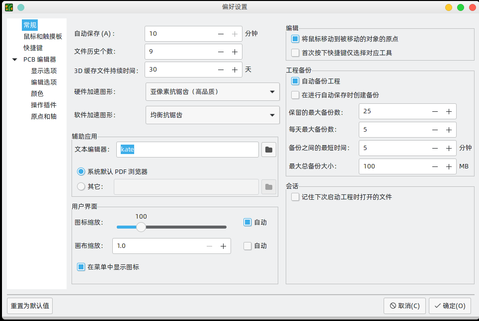
Pcbnew 有各种偏好设置,可以通过偏好设置对话框进行配置。与 KiCad 的所有部分一样,Pcbnew 的偏好设置存储在用户配置目录中,并且在 KiCad 次要版本之间相互独立,从而允许多个版本与独立的偏好设置并行运行。
偏好设置对话框的第一部分 (通用、鼠标和触摸板以及快捷键) 在所有 KiCad 程序之间共享。KiCad 手册中“通用偏好设置”部分详细介绍了这些部分。请注意,尽管快捷键部分在所有程序之间共享,但有许多特定于 Pcbnew 的快捷键只有在 Pcbnew 运行时才会出现在列表中。
显示选项
渲染引擎: 控制是否使用硬件加速图形或软件加速图形。
网格样式: 控制如何绘制路线网格。
网格厚度: 控制网格线或网格点的粗细。
最小网格间距: 控制两条网格线之间的最小距离 (以像素为单位)。无论当前的栅格设置如何,都不会绘制违反此最小间距的栅格线。
捕捉到网格: 控制何时将绘制和编辑操作捕捉到活动网格上的坐标。 “始终”将启用对齐,即使网格处于隐藏状态; “当网格显示时”将仅在网格可见时启用对齐。
| 按住 Ctrl 可以暂时禁用网格捕捉。 |
光标形状: 控制编辑光标是绘制为小十字准线还是全屏十字准线 (覆盖整个绘图画布的一组线)。 编辑光标显示下一个绘图或编辑操作将发生的位置,如果启用了捕捉,则会捕捉到栅格位置。
始终显示十字准线: 控制是始终显示编辑光标, 还是仅在编辑或绘图工具处于活动状态时才显示编辑光标。
网络名称: 控制是否在铜对象上绘制网络名称标签。 这些标签仅作为编辑指南,不会出现在制造输出中。
显示焊盘编号:控制是否在封装焊盘上绘制焊盘编号标签。
显示焊盘 <无网络> 指示器: 控制是否用特殊标记指示没有 网络的焊盘。
布线间隙: 控制是否显示布线和过孔周围的间隙轮廓。 间隙轮廓显示为对象周围的细长形状,表示与其他对象之间的最小间隙, 如约束和设计规则所定义。
显示焊盘间隙: 控制是否显示焊盘周围的间隙轮廓。
交叉探测项的居中视图: 当 Eesschema 和 Pcbnew 都在运行时, 控制点击 Eesschema 中的元件或引脚是否会使 Pcbnew 视图在相应的封装或焊盘上居中。
缩放以适合交叉探测项: 控制是否缩放视图以显示交叉探测 封装或焊盘。
高亮显示交叉探测网络: 控制当在两个工具中激活高亮显示工具时, 是否在 Pcbnew 中高亮显示 Eesschema 中高亮显示的网络。
编辑选项
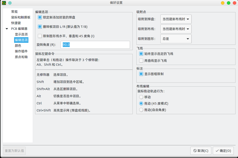
翻转电路板项目 L/R: 控制在顶层和底层之间移动电路板项目时翻转的方向。 选中时,项目从左向右翻转(围绕垂直轴); 取消选中时,项目从上向下翻转(围绕水平轴)。
旋转命令的步长: 控制每次使用旋转命令时选定对象将旋转多远。
允许自由焊盘: 控制封装焊盘是否可以解锁并与封装分开编辑或移动。
Magnetic points: This section controls object snapping, also called magnetic points. Object snapping takes precedence over grid snapping when it is enabled. Object snapping only works to objects on the active layer. Hold Shift to temporarily disable object snapping.
捕捉焊盘: 控制编辑光标何时捕捉焊盘原点。
捕捉到布线: 控制编辑光标何时捕捉到布线端点。
对齐图形: 控制编辑光标何时对齐图形形状点。
始终显示选定的飞线:启用后,即使全局飞线被隐藏, 选定封装外形的飞线也将始终显示。
用曲线显示飞线:控制飞线是直线绘制还是曲线绘制。
鼠标拖动布线行为: 控制使用鼠标拖动布线段时将发生的操作:"移动" 将独立于任何其他布线段移动布线。 "拖动(45 度模式)" 将调用推挤式布线器拖动布线,遵守设计规则并保持其他布线段的连接。 "拖动(自由角度)" 将移动布线段最近的角点,高亮显示与其他对象的碰撞,但不会将其移开。
将图形线条限制为 H、V 和45度: 控制使用图形绘制工具绘制的布线是否可以采用任何角度。 请注意,这仅影响绘制新的布线:可以编辑布线以采用任何角度。
显示页面限制: 控制页面边界是否绘制为矩形。
覆铜属性后重新填充覆铜对话框: 控制编辑任何覆铜的属性后是否自动重新填充覆铜。 可以在复杂的设计或速度较慢的计算机上禁用此功能,以提高响应速度。
颜色
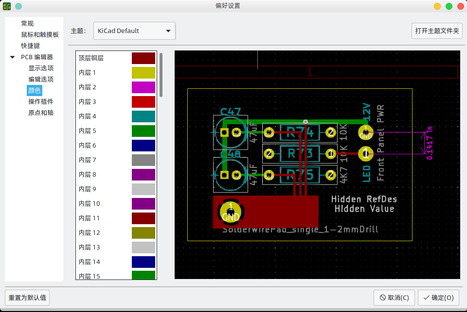
Pcbnew 支持在不同的颜色主题之间切换,以符合您的喜好。Kicad 6.0 有两个内置的颜色主题:"KiCad 默认" 是一个新主题,设计用于大多数情况下具有良好的对比度和平衡度,并且是新安装的默认主题。"KiCad 经典版" 是 KiCad 5.1 及更早版本的默认主题。这两个内置主题都不能修改,但您可以创建新主题来自定义 Pcbnew 的外观,也可以安装其他用户制作的主题。
颜色主题存储在位于 KiCad 配置目录的 Colors 子目录中的 JSON 文件中。“打开主题文件夹”按钮将在您的系统文件管理器中打开此位置,使您可以轻松地管理已安装的主题。要安装新主题,请将其放在此文件夹中,然后重新启动 KiCad。如果文件是有效的颜色主题文件,则新主题将从颜色主题下拉列表中提供。
要创建一个新的颜色主题,从颜色主题的下拉列表中选择新主题…。 为你的主题输入一个名称,然后开始编辑颜色。 新主题中的颜色将从你创建新主题之前选择的任何主题中复制。
要更改颜色,请双击或中键单击列表中的色样。“重置为默认值”按钮会将该颜色重置为“KiCad 默认”颜色主题中的相应条目。
颜色主题会自动保存;当您关闭偏好设置对话框时,所有更改都会立即反映出来。对话框右侧的窗口显示所选主题外观的预览。
操作插件
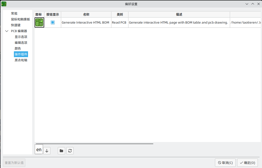
KiCad PCB 编辑器支持用 Python 编写的插件,可以对正在编辑的电路板进行操作。 这些插件可以使用内置的插件和内容管理器来安装(详见 KiCad 章节),或者将插件文件放在用户的插件目录中。 详见下面的脚本部分。
每个被检测到的插件都会在这个偏好设置上显示一排。 插件可以在 PCB 编辑器的顶部工具栏上显示一个按钮。 如果一个插件的 "显示按钮" 控制没有被选中,它仍然可以从 "工具" > "外部插件" 菜单中访问。
列表底部的箭头控制允许改变插件在工具栏和菜单中的显示顺序。 文件夹按钮将启动一个文件资源管理器到插件文件夹,以使安装新的插件更容易。 刷新按钮将扫描插件文件夹中的任何新的或删除的插件,并更新列表。
原点和轴
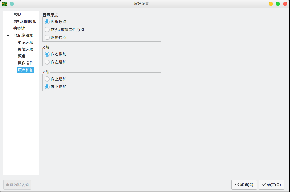
显示原点: 决定在编辑画布中坐标显示使用哪个坐标原点。 页面原点固定在页面的角落。 用户可以移动钻取/放置文件原点和栅格原点。
X 轴: 控制 X 坐标向右还是向左增加。
Y 轴: 控制 Y 坐标是向上还是向下增加。
自定义设计规则
KiCad’s custom design rule system allows creating design rules that are more specific than the generic rules available in the Constraints page of the Board Setup dialog. Custom design rules have many applications, but in general they are used to apply certain rules to a portion of the board, such as a specific net or netclass, a specific area, or a specific footprint.
自定义设计规则存储在一个扩展名为 kicad_dra 的单独文件中。当您开始向项目添加自定义规则时,会自动创建此文件。如果您在项目中使用自定义规则,请在备份或提交到版本控制系统时,确保将 kicad_dra 文件与 kicad_pcb 和 kicad_pro 文件一起保存。
kicad_dra 文件由 KiCad 自动管理,不应使用外部文本编辑器进行编辑。
始终使用电路板设置对话框的自定义规则页面编辑自定义设计规则。
|
自定义规则编辑器
自定义规则编辑器位于电路板设置对话框中,它提供了一个用于输入自定义规则的文本编辑器,一个语法检查器将测试你的自定义规则并指出任何错误,还有一个语法帮助对话框,其中包含了对自定义规则语言的快速参考和一些规则示例。
最好在编辑自定义规则后使用 检查规则语法 按钮,以确保没有语法错误。自定义规则中的任何错误都将阻止设计规则检查器运行。
自定义规则语法
自定义设计规则语言基于 s 表达式,允许您创建使用内置约束无法实现的设计约束。每条设计规则通常包含一个定义匹配哪些对象的 条件,以及一个定义要应用于匹配对象的规则的 约束。
该语言使用圆括号 (( 和 )) 来定义相关标记和值的子句。括号必须始终匹配:对于每个 ( 必须有匹配的 )。在子句中,标记和值之间用空格分隔。按照惯例,使用单个空格,但是可以在标记之间使用任意数量的空格字符。在文本字符串有效的地方,没有任何空格的字符串可以用 " 或 ' 引起来,也可以不加引号。包含空格的字符串必须始终用引号引起来。在需要嵌套引号的地方,可以使用 " 作为外引号字符,使用 ' 作为内引号字符 (反之亦然),从而实现单层嵌套。换行符不是必需的,但为清楚起见,通常在示例中使用。
在下面的语法描述中,< 尖括号 > 中的项表示必须存在的标记,[ 方括号 ] 中的项表示可选或仅有时需要的标记。
自定义规则文件必须以定义规则语言的版本头开始。 从 KiCad 6.0 开始,版本是 1。 版本头的语法是 (version<number>)。因此,在 KiCad 6.0 中,标题应该是这样的:
(version 1)
在版本标题之后,您可以输入任意数量的规则。规则以相反的顺序计算,这意味着首先检查文件中的最后一个规则。一旦找到正在测试的给定集合对象的匹配规则,将不再检查其他规则。实际上,这意味着更具体的规则应该在文件的后面,以便在评估更一般的规则之前对其进行评估。
例如,如果您创建一条规则来限制网络 HV 中的布线与任何其他网络中的布线之间的最小间距,以及第二条规则来限制特定规则区域内所有对象的最小间距,请确保第一条规则在自定义规则文件中的出现时间比第二条规则晚,否则,如果 HV 网络中的布线落在规则区域内,可能会有错误的间距。
每条规则必须有一个名称和一个或多个 约束 (constraint) 子句。该名称可以是任何字符串,用于在 DRC 报告中引用该规则。约束 (constraint) 定义了规则的行为。规则还可以有一个 条件 (condition) 子句,决定哪些对象应该应用该规则,以及一个可选的 层 (layer) 子句,指定该规则适用于哪些板层。
(rule <name>
    [(layer <layer_name>)]
    [(condition <expression>)]
    (constraint <constraint_type> [constraint_arguments]))
定制规则文件还可以包括描述规则的注释。注释由任何以 # 字符开头的行表示 (不包括空格)。
# Clearance for 400V nets to anything else
# 400V 网络与任何其他网络之间的净空
(rule HV
    (condition "A.NetClass == 'HV'")
    (constraint clearance (min 1.5mm))))
图层子句
层 (layer) 子句确定规则将对哪些层起作用。虽然对象层可以在下面介绍的 约束 (constraint) 子句中进行测试,但是使用 层 (layer) 子句效率更高。
层 (layer) 子句的值可以是任何线路板层名,也可以是与顶底铜层 ( F.Cu 和 B.Cu ) 匹配的快捷方式 外 (outer),以及与任何内部铜层匹配的快捷键 内 (inner)。
如果省略 层 (layer) 子句,则该规则将适用于所有层。
下面是一些示例:
# Do not allow footprints on back layer (no condition clause means this rule always applies)
# 不允许在底层上留下封装 (无条件子句表示此规则始终适用)
(rule "Top side footprints only"
    (layer B.Cu)
    (constraint disallow footprint))

# This rule does the same thing, but is less efficient
# 此规则执行相同的操作,但效率较低
(rule "Top side footprints only"
    (condition "A.Layer == 'B.Cu'")
    (constraint disallow footprint))

# Larger clearance on outer layers (inner layer clearance set by board minimum clearance)
# 外层间隙较大 (内层间隙由电路板最小间隙设置)
(rule "clearance_outer"
    (layer outer)
    (constraint clearance (min 0.25mm)))
条件子句
规则 条件 是一个包含在文本字符串中的表达式(因此通常用引号包围,以便允许留出空白,使之更清晰)。 该表达式是针对设计规则检查器正在测试的每一对对象进行评估的。 例如,当检查铜对象之间的间隙时,每个网络上的每个铜对象(布线段、焊盘、通孔等)都要与其他网络上的其他铜对象进行检查。 如果存在一个自定义规则,其表达式与两个给定的铜对象相匹配,并且约束条件定义了铜的间隙,那么这个自定义规则可以用来确定这两个对象之间所需的间隙。
被测对象在表达式语言中称为 A 和 B。这两个对象的顺序并不重要,因为设计规则检查器将测试这两种可能的顺序。例如,您可以编写一条规则,假设 A 为布线,B 为过孔。 有一些表达式函数可以同时测试这两个对象;这些表达式函数使用 AB 作为对象名。
条件中的表达式必须解析为布尔值 ( 真 (true 或 false )。如果表达式解析为 true,则规则应用于给定的对象。
每个被测对象都有可以比较的 属性,以及可以执行特定测试的 函数。属性和函数的使用语法分别为 <object>.<property> 和 <object>.<function>([arguments])。译者注: <对象>.<属性> 和 <对象>.<函数>([参数])。
当您在文本编辑器 ( A.、B. 或 AB. ) 中键入 <对象 (object)>. 时,会出现一个自动完成列表。将打开包含所有可使用的对象属性的。
|
使用 布尔运算符 比较对象属性和函数,得到布尔表达式。布尔运算符基于 C/C++ 语法,并支持以下运算符:
|
等于 |
|
不等于 |
|
大于、大于或等于 |
|
小于、小于或等于 |
|
和 |
|
或 |
例如,A.NetClass == 'HV' 将适用于任何属于 "HV" 网类的对象,A.NetClass != B.NetClass 将适用于任何属于不同网类的对象。圆括号可以用来澄清复杂表达式中的操作顺序,但并不是必须的。
有些属性表示物理测量,比如尺寸、角度、长度、位置等等。 在这些属性上,单位后缀 可以在自定义规则语言中使用,以指定使用什么单位。 如果没有使用单位后缀,属性的内部表示将被使用(距离为纳米,大多数角度为度)。 支持以下后缀:
|
毫米 |
|
千分之一英寸 (mils) |
|
英寸 |
|
度 |
|
弧度 |
| 自定义设计规则中使用的单位独立于 PCB 编辑器中的显示单位。 |
约束
规则的 约束 子句定义了规则在条件匹配的对象上的行为。每个约束子句都有一个 约束类型 和一个或多个设置约束行为的参数。单个规则可以有多个约束子句,以便为符合相同规则条件的对象设置多个约束 (如 间隙 (clearance)、布线宽度 (trace_width) )。
许多约束条件的参数指定了一个物理测量或数量。 这些约束条件支持最小值、最优值和最大值说明(缩写为 "min/opt/max")。 最小 和 最大 值用于设计规则检查:如果实际值小于约束条件中的最小值或大于最大值,将产生一个 DRC 错误。 最优 值仅用于某些约束,并通知 KiCad 默认使用的 "最优" 值。 例如,最优的 diff_pair_gap 是由布线器在放置新的差分对时使用的。 如果后来修改了差分对,使得差分对之间的间隙与最佳值不同,只要间隙在最小值和最大值之间(如果这些值被指定),就不会产生错误。 在所有接受最小/最大/最优值的情况下,可以指定任何或全部的最小值、最优值和最大值。
最小/最优/最大值被指定为 (min<value>), (opt<value>), 和 (max<value>)。例如,布线宽度约束可以写成 (constraint track_width (min 0.5mm) (opt 0.5mm) (max 1.0mm)),如果只约束最小宽度,可以简单写成 `(constraint track_width (min 0.5mm))。
| Constraint type | Argument type | Description |
|---|---|---|
|
min/opt/max |
Checks the width of annular rings on vias. |
|
min |
Checks the clearance between copper objects of different nets. KiCad’s design rule system does not permit constraining clearance between objects on the same net at this time. To allow copper objects to overlap (collide), create a |
|
min |
Checks the clearance between footprint courtyards and generates an error if any two courtyards
are closer than the |
|
min/opt/max |
Checks the gap between coupled tracks in a differential pair. Coupled tracks are segments that are parallel to each other. Differential pair gap is not tested on uncoupled portions of a differential pair (for example, the fanout from a component). |
|
max |
Checks the distance that a differential pair track is routed uncoupled from the other polarity track in the pair (for example, where the pair fans out from a component, or becomes uncoupled to pass around another object such as a via). |
|
|
Specify one or more object types to disallow, separated by spaces. For example,
|
|
min/opt/max |
Checks the clearance between objects and graphical items on the |
|
min/max |
Checks the total routed length for the nets that match the rule condition and generates an
error for each net that is below the |
|
min/max |
Checks the size (diameter) of a drilled hole in a pad or via. For oval holes, the smaller
(minor) diameter will be tested against the |
|
min |
Checks the clearance between a drilled hole in a pad or via and copper objects on a different net. The clearance is measured from the diameter of the hole, not its center. |
|
min |
Checks the clearance between mechanically-drilled holes in pads and vias. The clearance is measured between the diameters of the holes, not between their centers. HDI vias (microvias, blind vias, and buried vias) are not tested by this constraint. |
|
min/opt/max |
Checks the clearance between objects on silkscreen layers and other objects. |
|
max |
Checks the total skew for the nets that match the rule condition, that is, the difference
between the length of each net and the average of all the lengths of each net that is matched
by the rule. If the absolute value of the difference between that average and the length of
any one net is above the constraint |
|
min/opt/max |
Checks the width of track and arc segments. An error will be generated for each segment that
has a width below the |
|
max |
Counts the number of vias on every net matched by the rule condition. If that number exceeds
the constraint |
对象属性和函数参考
可以在自定义规则表达式中测试以下属性:
常见属性
这些属性适用于所有 PCB 对象。
| 属性 | 数据类型 | 描述 |
|---|---|---|
|
string |
对象所在的板层。对于存在于多个层上的对象,
该属性将返回第一层 (例如,对于大多数通孔焊盘/通孔,返回 |
|
boolean |
如果对象已锁定,则为 True。 |
|
string |
返回此对象的父对象的唯一标识符。 |
|
dimension |
对象原点在 X 轴上的位置。请注意,对象的原点并不总是与对象边界框的中心相同。 例如,封装的原点是封装编辑器中该封装的 (0, 0) 坐标的位置, 但是封装的设计可能使此位置不在外框形状的中心。 |
|
dimension |
对象原点在 Y 轴上的位置。请注意,KiCad 始终在内部使用从屏幕顶部到底部递增的 Y 坐标, 即使您已将设置配置为显示从底部到顶部递增的 Y 坐标。 |
|
string |
"封装 (Footprint)", "焊盘 (Pad)", "图形形状 (Graphic Shape)", "电路板文本 (Board Text)", "封装文本 (Footprint Text)", "敷铜 (Zone)", "布线 (Track)", "过孔 (Via)", "敷铜 (Zone)", 或 "组合 (Group)" 之一. |
连接的对象属性
这些属性适用于可以分配网的铜对象(焊盘、过孔、覆铜、布线)。
| 属性 | 数据类型 | 描述 |
|---|---|---|
|
integer |
铜对象的网络码。 请注意,不能依赖网络码来保持不变:如果您需要在规则中引用特定的网络,请使用`NetName`。
|
|
string |
铜对象的网络类的名称。 |
|
string |
铜对象的网络名称。 |
封装属性
These properties apply to footprints.
| 属性 | 数据类型 | 描述 |
|---|---|---|
|
dimension |
为封装设置的铜间隙覆盖。 |
|
double |
封装的方向 (旋转) (单位:度)。 |
|
string |
封装的位号。 |
|
dimension |
为封装设置的焊膏边缘覆盖。 |
|
dimension |
为封装设置的焊膏余量比率覆盖。 |
|
dimension |
为封转设置的散热间隙。 |
|
dimension |
为封装设置的散热连接宽度。 |
|
string |
封装的 "值" 字段的内容。 |
焊盘属性
These properties apply to footprint pads.
| 属性 | 数据类型 | 描述 |
|---|---|---|
|
dimension |
为焊盘设置的铜间隙覆盖。 |
|
string |
"无"、"BGA 焊盘"、"基准, 全局到电路板"、"基准, 本地到封装"、"测试点焊盘"、 "散热片焊盘"、"蜂窝状焊盘" 之一。 |
|
dimension |
焊盘在 X 轴上的通孔/槽的大小。 |
|
dimension |
焊盘在 Y 轴上的通孔/槽的大小。 |
|
double |
焊盘的方向 (旋转) (单位:度)。 |
|
string |
焊盘的 "编号",可以是字符串 (例如,BGA 中的 "A1")。 |
|
dimension |
焊盘的 "焊盘到芯片长度" 属性的值,它是在计算网络时添加到焊盘的网络的附加长度。 |
|
string |
"通孔"、"贴片"、"板边连接器" 或 "非导通孔,机械" 之一。 |
|
string |
焊盘的名称 (通常是原理图中相应接点的名称)。 |
|
string |
焊盘的电气类型 (通常取自原理图中相应的引脚)。 "输入"、"输出"、"双向"、"三态"、"无源"、"自由"、"未指定"、 "电源输入"、"电源输出"、"集电极开路"、"发射器开路" 或 "未连接" 之一。 |
|
double |
对于圆形矩形焊盘,为半径与矩形大小的比率。 |
|
string |
"圆形"、"矩形"、"椭圆形"、"梯形"、"圆角矩形"、"倒角矩形" 或 "自定义" 之一。 |
|
dimension |
焊盘在 X 轴上的大小。 |
|
dimension |
焊盘在 Y 轴上的大小。 |
|
dimension |
为焊盘设置的阻焊边距覆盖。 |
|
dimension |
为焊盘设置的焊膏边距覆盖。 |
|
dimension |
为焊盘设置的焊膏边距比率覆盖。 |
|
dimension |
为焊盘设置的散热间隙。 |
|
dimension |
为焊盘设置的散热连接宽度。 |
布线和圆弧属性
These properties apply to tracks and arc tracks.
| 属性 | 数据类型 | 描述 |
|---|---|---|
|
dimension |
起点的 X 坐标。 |
|
dimension |
起点的 Y 坐标。 |
|
dimension |
终点的 X 坐标。 |
|
dimension |
终点的 Y 坐标。 |
|
dimension |
布线或圆弧的宽度。 |
过孔属性
These properties apply to vias.
| 属性 | 数据类型 | 描述 |
|---|---|---|
|
dimension |
过孔焊盘的直径。 |
|
dimension |
过孔成品通孔的直径。 |
|
string |
过孔压层中的最后一层。 |
|
string |
过孔压层中的第一层。 |
|
string |
"通孔"、"盲孔/埋孔" 或 "微孔" 之一。 |
覆铜和规则区域属性
这些属性适用于铜区和非铜区,以及规则区(以前称为禁止布线区)。
| 属性 | 数据类型 | 描述 |
|---|---|---|
|
dimension |
为覆铜设置的铜间隙覆盖。 |
|
dimension |
覆铜中允许的填充区域的最小宽度。 |
|
string |
用户指定的名称 (默认情况下为空)。 |
|
string |
"继承"、"无"、"焊盘散热孔"、"实心"、"导通的散热孔" 之一 |
|
int |
覆铜的优先级别。 |
|
dimension |
为覆铜设置的散热间隙。 |
|
dimension |
为覆铜设置的散热连接宽度。 |
图形形状属性
这些属性适用于图形线、圆弧、圆、矩形和多边形。
| 属性 | 数据类型 | 描述 |
|---|---|---|
|
dimension |
终点的 X 坐标。 |
|
dimension |
终点的 Y 坐标。 |
|
dimension |
形状画笔的粗细。 |
文本属性
这些属性适用于文本对象(封装字段、自由文本标签等)。
| 属性 | 数据类型 | 描述 |
|---|---|---|
|
boolean |
如果文本为粗体,则为 |
|
dimension |
字体中字符的高度。 |
|
string |
水平文本对齐 (对齐):"向左对齐"、"居中对齐" 或 "向右对齐" 之一。 |
|
boolean |
如果文本为斜体,则为 |
|
boolean |
如果文本为镜像,则为 |
|
string |
文本对象的内容。 |
|
dimension |
字体笔划的粗细。 |
|
dimension |
字体中字符的宽度。 |
|
string |
垂直文本对齐方式:"向上对齐"、"居中对齐" 或 "向下对齐" 之一。 |
|
boolean |
如果文本对象可见 (显示),则为 |
表达式函数
可以对自定义规则表达式中的对象调用以下函数:
| Function | Objects | Description |
|---|---|---|
|
|
Returns true if the object exists on the given board layer. |
|
|
Returns true if the object exists on the copper path between the given pads. |
|
|
Returns true if the object is part of a differential pair and the base name of the pair
matches the given argument |
|
|
Returns true if any part of the object is inside the named rule area or zone. Rule area and zone names can be set in their respective properties dialogs. If the given area is a filled copper zone, the function tests if the given object is inside any of the filled copper regions of the zone, not if the object is inside the zone’s outline. |
|
|
Returns true if the any part of the object is inside the courtyard of the given footprint reference. The
first variant checks both the front or back courtyard and returns true if the object is inside
either one; the second and third variants check a specific courtyard. The |
|
|
Returns true if the object is a blind/buried via. |
|
|
Returns true if the two objects being tested are part of the same differential pair but are
opposite polarities. For example, returns true if |
|
|
Returns true if the object is a microvia. |
|
|
Returns true if the object is a plated hole (in a pad or via). |
|
|
Returns true if the object is a member of the named group |
自定义设计规则示例
(rule RF_width
	(layer outer)
	(condition "A.NetClass == 'RF'")
	(constraint track_width (min 0.35mm) (max 0.35mm)))

(rule "BGA neckdown"
	(constraint track_width (min 0.2mm) (opt 0.25mm))
	(constraint clearance (min 0.05mm) (opt 0.08mm))
	(condition "A.insideCourtyard('U3')"))

(rule "Distance between Vias of Different Nets"
	(constraint hole_to_hole (min 0.25mm))
	(condition "A.Type =='Via' && B.Type =='Via' && A.Net != B.Net"))

(rule "Distance between test points"
	(constraint courtyard_clearance (min 1.5mm))
	(condition "A.Reference =='TP*' && B.Reference == 'TP*"))

# This assumes that there is a cutout with 1mm thick lines
# 这假设有一个带有 1mm 粗细的打断
(rule "Clearance to cutout"
	(constraint clearance (min 0.8mm))
	(condition "A.Layer=='Edge.Cuts' && A.Thickness == 1.0mm"))

(rule "Max Drill Hole Size Mechanical"
	(constraint hole (max 6.3mm))
	(condition "A.Pad_Type == 'NPTH, mechanical'"))

(rule "Max Drill Hole Size PTH"
	(constraint hole (max 6.35mm))
	(condition "A.Pad_Type == 'Through-hole'"))

# Specify an optimal gap for a particular differential pair
(rule "Clock gap"
	(condition "A.inDiffPair('/CLK')")
	(constraint diff_pair_gap (opt 0.8mm)))

# Specify a larger clearance between differential pairs and anything else
# 指定差分对之间的较大间隙和任何其他间隙
(rule "Differential pair clearance"
	(condition "A.inDiffPair('*') && !AB.isCoupledDiffPair()")
	(constraint clearance (min 1.5mm)))
脚本
脚本允许您使用 Python 语言自动执行 KiCad 中的任务。可以通过 Python "操作插件" 向 KiCad 添加功能,这些插件可以添加到顶部工具栏。也可以编写与 KiCad 文件交互的独立脚本,例如,从电路板文件自动生成制造输出。
本手册涵盖了一般脚本编写概念。希望编写或修改脚本的用户还应使用 https://docs.kicad.org/doxygen-python/namespaces.html 上的 Doxygen 文档。
KiCad 6 或更新版本需要 Python 3 来支持脚本。Python 2 已不再被支持。
Python 脚本位置
PCB 编辑器的插件脚本可以通过插件和内容管理器(PCM)自动安装,也可以通过手动将插件复制到一个文件夹中。 每个插件都应该在 plugins 文件夹内有自己的文件夹。 plugins 文件夹的位置默认为:
| 平台 | 路径 |
|---|---|
Linx |
|
macOS |
|
Windows |
|
操作插件
| TODO:编写本部分 (如何安装新的操作插件) |
封装向导
封装向导是可以从封装编辑器访问的 Python 脚本的集合。 如果调用封装对话框,则选择一个给定的向导,该向导允许您查看渲染的封装,并且您可以编辑一些参数。
如果插件未正确分发到您的系统软件包,您可以在 KiCad 源代码树中的链接中找到最新版本:https://gitlab.com/kicad/code/kicad/tree/master/pcbnew/python/plugins[gitlab]。
使用脚本控制台
Pcbnew comes with a built-in Python console that can be used to inspect and interact with the board. To launch the console, use the ![]() button in the top toolbar. The Pcbnew Python API is not automatically loaded, so to load it, type
button in the top toolbar. The Pcbnew Python API is not automatically loaded, so to load it, type import pcbnew into the console. The command pcbnew.GetBoard() will then return a reference to the board currently loaded in Pcbnew, which can be inspected and modified through the console.
| TODO:记录其他有用的 PyAlaMode 函数 |
编写外部脚本
| TODO:写下这一节 |
编写操作插件
| TODO:写下这一节 |
Working With IDF Component Outlines
KiCad can export an IDF representation of the board for use in mechanical CAD software. Below is some guidance on attaching IDF component outlines to footprints, creating new IDF component outlines, and a description of the IDF utilities included with KiCad.
Specifying component models for use by the exporter
IDF component models are attached to footprints using the footprint’s 3D model properties. The IDF exporter uses different filetypes than the 3D viewer and other 3D model exporters, so adding 3D models for the IDF exporter does not conflict with 3D models added to a footprint for other purposes.
To add an IDF model to a footprint in the footprint or PCB editors, edit the footprint’s properties and click on the 3D Models tab.
Click the ![]() button and select the IDF (*.idf;*.IDF) filetype filter. Browse to the desired outline file.
button and select the IDF (*.idf;*.IDF) filetype filter. Browse to the desired outline file.
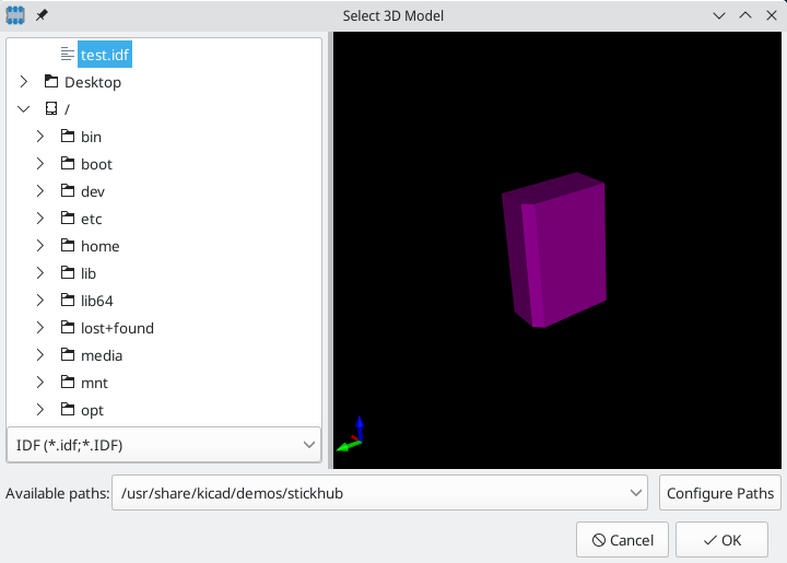
Once the desired component outline file is selected, enter any necessary values for the offset and rotation. The offsets must be specified using the IDF board output units (mm or mils) and in the IDF coordinate system, which is a right-hand coordinate system with +Z pointing towards the viewer, +X to the viewer’s right, and +Y towards the upper edge of the screen. The rotation must be in degrees; positive rotation is a counter-clockwise rotation as described in the IDFv3 specification.
Multiple outlines may be combined with appropriate offsets to represent simple assemblies such as a DIP package in a socket.
| Only the offset values and the Z rotation value are used by the IDF exporter; all other values are ignored. |
Creating a component outline file
The component outline file (*.idf) consists of a single .ELECTRICAL or .MECHANICAL section as described in the specification document. The section may be preceded by any number of comment lines; the comment lines are copied by the exporter into the library file and can be used to track metadata such as references to the documents used to determine the component’s outline and dimensions.
The component outline section contains fields which are strings, integers, or floating point numbers. A string is a combination of characters which may include spaces; if a string contains spaces then it must be quoted. Quotation marks must not appear within a string. Floating point numbers may be represented using decimal or exponential notations but decimal notation is preferred for human readability. The decimal point must be a dot and not a comma. The IDF file must consist only of 7-bit ASCII characters; use of 8-bit characters will result in undefined behavior.
An IDF file consists of SECTIONS which consist of RECORDS which consist of FIELDS. For the IDF outline files only one type of section may exist and must be one of .ELECTRICAL or .MECHANICAL. A record is a single line of text and may contain one or more fields. Fields are sequences of characters separated by one or more spaces which do not appear between quotation marks. All fields of a record must appear on a single line; records may not span lines.
The section heading (.ELECTRICAL or .MECHANICAL) is considered the first record (Record 1) of the section. Record 1 must be followed by Record 2 which has four fields:
-
Geometry Name: a string which in combination with the Part Number must form a unique identifier for the component outline. For standardized packages, the package name is a good value for the geometry name, for example "SOT-23". For unique packages the manufacturer’s part number is a good choice for the geometry name.
-
Part Number: although obviously intended for the part number, for example BS107, it is better to use this string to help describe the package. For example if the geometry name is "TO-92", the part number entry may be used to describe the layout of the pads or the orientation of this particular TO-92 outline file.
-
IDF Unit: this must be one of
MMorTHOUand it applies only to the units describing this single component outline. -
Height: this is a floating point number representing the nominal height of the component using units specified in Field 3.
Record 2 must be followed by a number of Record 3 entries which specify the outline of the component. Record 3 consists of four fields:
-
Loop Index:
0(outline points are specified in counter-clockwise order) or1(outline points are specified in clockwise order) -
X coordinate: a floating point number
-
Y coordinate: a floating point number
-
Included Angle: a floating point number. If the value is
0then a straight line segment is drawn from the previous point to this point. If the value is360then the previous point specifies the center of a circle and this point specifies a point on the circle; never specify a circle using a value of-360as at least one major mechanical CAD package does not behave well in that situation. If the value is negative then a clockwise arc is drawn from the previous point to this point and if the value is positive then a counter-clockwise arc is drawn.
Only one closed loop is permitted and it is not possible to specify a cutout. The last point specified must be the same as the first point unless the outline is a circle.
Example IDF File 1:
# a simple cylinder - this could represent an electrolytic capacitor
.ELECTRICAL
    "cylinder" "5mm OD, 5mm height" MM 5
    0 0 0 0
    0 2.5 0 360
.END_ELECTRICAL
Example IDF File 2:
# an upside-down T
# a comment added for the sake of adding comments
.ELECTRICAL
    "Capital T" "5x8x10mm, upside down" MM 10
    0 -0.5 8 0
    0 -0.5 0.5 0
    0 -2.5 0.5 0
    0 -2.5 -0.5 180
    0 2.5 -0.5 0
    0 2.5 0.5 180
    0 0.5 0.5 0
    0 0.5 8 0
    0 -0.5 8 180
.END_ELECTRICAL
Guidelines for creating outlines
When creating outlines, and especially when sharing the work with others, consistency in the design and naming of files helps people locate files quicker and place the components with minimal hassles.
Package naming
Try to make some information about the outline available in the filename to give the user a general idea of what the outline is. For example axial leaded cylindrical packages may represent some types of capacitors as well as some types of resistors, so it makes sense to identify an outline as a horizontal or vertical axial leaded device and to add some extra information on the relevant dimensions: diameter, length, and pitch are the most important. If a device has a unique outline, the manufacturer’s part number and a prefix to indicate the class of device are adequate.
Comments
Use comments in the IDF file to give users more information about the outline, for example a reference to the source used for dimensional information.
Geometry and Part Number entries
Think carefully about the values to give to the Geometry and Part Number entries. Taken together, these strings act as a unique identifier for the MCAD system. The values of the strings will ideally have some meaning to a user, but this is not necessary: the values are primarily intended for the MCAD system to use as a unique ID. Ideally the values chosen will be unique within any large collection of outlines; choosing values well will result in fewer clashes especially in complex boards.
Pin orientation and positioning
Component outlines should be created to match the orientation and position of the corresponding footprints. This avoids the need to specify a non-zero rotation for the IDF component outline. Since the IDF exporter ignores the (X, Y) offset values, it is vital that you use the correct origin in the IDF component outline.
The image above shows sample outlines generated by the programs idfcyl and idfrect and rendered in a mechanical CAD program. From left to right are (a) vertical radial leaded cylinder, (b) vertical axial leaded cylinder with wire on left, (c) vertical axial leaded cylinder with wire on right, (d) horizontal axial leaded cylinder, (e) horizontal radial leaded cylinder, (f) square outline, plain, (g) square outline with chamfer, (h) square outline with axial lead on right. The top outlines were specified in units of millimeters while the bottom outlines were specified in units of inches.
Tips on dimensions
The purpose served by the extruded outlines is to give the mechanical designer some idea of the location and physical space occupied by each component. In a typical scenario the mechanical designer will replace some of the crude outlines with more detailed mechanical models, for example when checking to ensure that a right-angle mounted LED will fit into a hole on a panel. In most situations the accuracy of an outline doesn’t matter, but it is good practice to create outlines which convey the best mechanical information possible. In a few instances a user may wish to fit the component into a case with very little excess space, for example in a portable music player. In such a situation, if most extruded outlines are a good enough representation of components then the mechanical designer may only have to replace very few models while designing the case. If the outlines are not a reliable reflection of reality then the mechanical designer will waste a lot of time replacing models to ensure a good fit. After all, if you put garbage in you can expect garbage to come out. If you put in good information, you can be confident of good results.
IDF Component Outline Tools
A number of command-line tools are available to help generate IDF component outlines. The tools are:
-
idfcyl:creates an outline of a cylinder in vertical or horizontal orientation and with axial or radial leads -
idfrect:creates an outline of a rectangle which may have either an axial lead or a chamfer in the top left corner -
dxf2idf:converts a drawing in DXF format into an IDF component outline
idfcyl
idfcyl generates outlines for cylindrical components.
When idfcyl is invoked with no arguments it prints out a usage note and a summary of its inputs:
idfcyl: This program generates an outline for a cylindrical component.
    The cylinder may be horizontal or vertical.
    A horizontal cylinder may have wires at one or both ends.
    A vertical cylinder may have at most one wire which may be
    placed on the left or right side.

Input:
    Unit: mm, in (millimeters or inches)
    Orientation: V (vertical)
    Lead type: X, R (axial, radial)
    Diameter of body
    Length of body
    Board offset
    *   Wire diameter
    *   Pitch
    **  Wire side: L, R (left, right)
    *** Lead length
    File name (must end in *.idf)

    NOTES:
        *   only required for horizontal orientation or
            vertical orientation with axial leads

        **  only required for vertical orientation with axial leads

        *** only required for horizontal orientation with radial leads
The notes can be suppressed by entering any arbitrary argument on the command line. A user can manually enter information at the command line or create scripts to generate outlines. The following script creates a single cylinder axial leaded outline with the lead on the right hand side:
#!/bin/bash
# Generate a cylindrical IDF outline for test purposes
# vertical 5mm cylinder,  nominal length 8mm + 3mm board offset,
# axial wire on right,  0.8mm wire dia., 3.5mm pitch
idfcyl - 1 > /dev/null <<  _EOF
mm
v
x
5
8
3
0.8
3.5
r
cylvmm_1R_D5_L8_Z3_WD0.8_P3.5.idf
_EOF
idfrect
idfrect generates outlines for rectangular components.
When idfrect is invoked with no arguments it prints out a usage note and a summary of its inputs:
idfrect: This program generates an outline for a rectangular component.
    The component may have a single lead (axial) or a chamfer on the
    upper left corner.
Input:
    Unit: mm, in (millimeters or inches)
    Width:
    Length:
    Height:
    Chamfer: length of the 45 deg. chamfer
    *  Leaded: Y,N (lead is always to the right)
    ** Wire diameter
    ** Pitch
    File name (must end in *.idf)

    NOTES:
        *   only required if chamfer = 0

        **  only required for leaded components
The notes can be suppressed by entering any arbitrary argument on the command line. A user can manually enter information at the command line or create scripts to generate outlines. The following script creates a chamfered rectangle and an axial leaded outline:
#!/bin/bash
# Generate various rectangular IDF outlines for test purposes
# 10x10, 1mm chamfer, 2mm height
idfrect - 1 > /dev/null <<  _EOF
mm
10
10
2
1
rectMM_10x10x2_C0.5.idf
_EOF
# 10x10x12,  0.8mm lead on 6mm pitch
idfrect - 1 > /dev/null <<  _EOF
mm
10
10
12
0
Y
0.8
6
rectLMM_10x10x12_D0.8_P6.0.idf
_EOF
dxf2idf
dxf2idf creates an IDF component file from a DXF outline.
The DXF file used to specify the component outline can be prepared with the free software LibreCAD for best compatibility.
When dxf2idf is invoked with no arguments it prints out a usage note and a summary of its inputs:
dxf2idf: this program takes line, arc, and circle segments
    from a DXF file and creates an IDF component outline file.

Input:
    DXF filename: the input file, must end in '.dxf'
    Units: mm, in (millimeters or inches)
    Geometry Name: string, as per IDF version 3.0 specification
    Part Name: as per IDF version 3.0 specification of Part Number
    Height: extruded height of the outline
    Comments: all non-empty lines are comments to be added to
        the IDF file. An empty line signifies the end of
        the comment block.
    File name: output filename, must end in '.idf'
The notes can be suppressed by entering any arbitrary argument on the command line. A user can manually enter information at the command line or create scripts to generate outlines. The following script creates a 5mm high outline from a DXF file test.dxf:
#!/bin/bash
# Generate an IDF outlines from a DXF file
dxf2idf - 1 > /dev/null << _EOF
test.dxf
mm
DXF TEST GEOMETRY
DXF TEST PART
5
This is an IDF test file produced from the outline 'test.dxf'
This is a second IDF comment to demonstrate multiple comments

test_dxf2idf.idf
_EOF
idf2vrml
The idf2vrml tool reads a set of one IDF Board (.emn) and one IDF Component file (.emp) and produces a VRML file which can be viewed with a VRML viewer. This feature is useful for visualization of the board assembly in cases where the user does not have access to MCAD software. Invoking idf2vrml without any arguments will result in the display of a usage message:
>./idf2vrml
Usage: idf2vrml -f input_file.emn -s scale_factor {-k} {-d} {-z} {-m}
flags:
   -k: produce KiCad-friendly VRML output; default is compact VRML
   -d: suppress substitution of default outlines
   -z: suppress rendering of zero-height outlines
   -m: print object mapping to stdout for debugging purposes
example to produce a model for use by KiCad: idf2vrml -f input.emn -s 0.3937008 -k
The idf2vrml tool does not correctly render OTHER_OUTLINE entities in an emn file if that entity is specified on the back layer of the PCB; however you will not noticeable using files exported by KiCad because there is no mechanism to specify such an entity. This is only an issue if you render a third party emn file which does employ an entity on the back side of a board.
|
操作参考
Below is a list of every available action in Pcbnew: a command that can be assigned to a hotkey.
PCB 编辑器
The actions below are available in Pcbnew. Hotkeys can be assigned to any of these actions in the Hotkeys section of the preferences.
| 操作 | 默认快捷键 | 说明 |
|---|---|---|
向下对齐 |
将选定项目与下边对齐 |
|
与垂直中心对齐 |
将选定项目垂直居中对齐 |
|
与水平中心对齐 |
将选定项目与水平中心对齐 |
|
向左对齐 |
将选定项目与左边对齐 |
|
向右对齐 |
将选定项目与右边对齐 |
|
向上对齐 |
将选定项目与上边对齐 |
|
水平分布 |
沿水平轴分布选定项目 |
|
垂直分布 |
沿垂直轴分布选定项目 |
|
放置电路板外封装 |
执行电路板区域外元件的自动放置 |
|
放置选择的封装 |
执行选择的元件的自动放置 |
|
翻转电路板视图 |
从反面看板 |
|
草图图形项目 |
在轮廓模式下显示图形项 |
|
降低图层不透明度 |
{ |
增加当前图层的透明度 |
增加图层不透明度 |
} |
降低当前图层的透明度 |
切换到元件 (F.Cu) 层 |
PgUp |
|
切换到内层 1 |
||
切换到内层 2 |
||
切换到内层 3 |
||
切换到内层 4 |
||
切换到内层 5 |
||
切换到内层 6 |
||
切换到内层 7 |
||
切换到内层 8 |
||
切换到内层 9 |
||
切换到内层 10 |
||
切换到内层 11 |
||
切换到内层 12 |
||
切换到内层 13 |
||
切换到内层 14 |
||
切换到内层 15 |
||
切换到内层 16 |
||
切换到内层 17 |
||
切换到内层 18 |
||
切换到内层 19 |
||
切换到内层 20 |
||
切换到内层 21 |
||
切换到内层 22 |
||
切换到内层 23 |
||
切换到内层 24 |
||
切换到内层 25 |
||
切换到内层 26 |
||
切换到内层 27 |
||
切换到内层 28 |
||
切换到内层 29 |
||
切换到内层 30 |
||
切换到铜 (B.Cu) 层 |
PgDn |
|
切换到下一层 |
+ |
|
切换到上一层 |
- |
|
切换图层 |
V |
在活动层对中的层之间切换 |
网络检查器 |
显示网络检查器 |
|
高亮飞线 |
显示所选项目的飞线 |
|
草图焊盘 |
在轮廓模式下显示焊盘 |
|
弯曲的飞线 |
用曲线显示飞线 |
|
修复电路板 |
运行各种诊断程序并尝试修复电路板 |
|
显示外观管理器 |
显示/隐藏外观管理器 |
|
显示焊盘编号 |
显示焊盘编号 |
|
脚本控制台 |
显示 Python 脚本控制台 |
|
显示飞线 |
显示电路板飞线 |
|
草图文本项 |
在行模式下显示封装文本 |
|
草图布线 |
K |
在轮廓模式下显示布线 |
草图过孔 |
在轮廓模式下显示过孔 |
|
线框区域 |
仅显示区域边界 |
|
填充覆铜 |
显示覆铜的填充区域 |
|
草图区域 |
在轮廓模式下显示分区的实心区域 |
|
切换区域显示 |
A |
在显示填充区域、线框区域和草图区域之间循环 |
自动缩放以适应 |
更改封装时缩放以适应 |
|
转换为圆弧 |
将选定的线段转换为圆弧 |
|
转换为规则区域 |
从所选内容创建规则区域 |
|
转换为线 |
从所选内容创建图形线 |
|
转换为多边形 |
从所选内容创建图形多边形 |
|
转换为布线 |
将选定的图形线转换为布线 |
|
转换为覆铜 |
从所选内容创建覆铜 |
|
设计规则检查 |
显示设计规则检查器窗口 |
|
在封装编辑器中打开 |
Ctrl+E |
在封装编辑器中打开选定的封装 |
附加电路板… |
打开另一个电路板并将其内容附加到此电路板上 |
|
电路板设置… |
编辑电路板设置,包括层、设计规则和各种默认设置。 |
|
清除网络高亮 |
~ |
清除任何现有网络高亮 |
钻孔/放置文件原点 |
放置钻孔文件和元件放置文件的原点 |
|
导出 Specctra DSN… |
导出 Specctra DSN 布线信息 |
|
BOM… |
从电路板创建 BOM 表 |
|
IPC-D-356 网表文件… |
生成 IPC-D-356 网表文件 |
|
钻孔文件 (.drl)… |
生成 Excellon 钻孔文件 |
|
Gerbers (.gbr)… |
为制造生成 Gerbers |
|
元件放置 (.pos)… |
为贴片和插件生成元件放置文件 |
|
封装报告 (.rpt)… |
从当前电路板创建所有封装的报告 |
|
组合 |
将所选项目组合,以便将它们作为单个项目处理 |
|
进入组合 |
进入要编辑项目的组合 |
|
离开组合 |
离开当前组合 |
|
隐藏网络 |
隐藏所选网络的飞线 |
|
高亮网络 |
` |
高亮网络中的所有铜项 |
高亮网络 |
高亮网络中的所有铜项 |
|
导入网表… |
读取网表并更新电路板连接 |
|
导入 Specctra 会话… |
导入布线的 Specctra session (*.ses) 文件 |
|
锁定 |
防止项目在画布上移动和/或调整大小 |
|
添加封装 |
O |
添加封装 |
添加图层对齐目标 |
添加图层对齐目标 |
|
删除项目 |
从组合中删除项目 |
|
切换到原理图编辑器 |
在 Eesschema 中打开原理图 |
|
显示网络 |
显示所选网络的飞线 |
|
切换上次网络高亮 |
在最后两个高亮的网络之间切换 |
|
切换锁定 |
L |
锁定或解锁选定项目 |
切换网络高光 |
Ctrl+` |
切换网络高亮 |
将布线宽度切换到上一个 |
Shift+W |
将布线宽度更改为上一个的预定义大小 |
将布线宽度切换到下一个 |
W |
将布线宽度更改为下一个的预定义大小 |
解组 |
取消对任何选定组的组合 |
|
解锁 |
允许在画布上移动和/或调整项目大小 |
|
减小过孔尺寸 |
\ |
将过孔尺寸更改为上一个的预定义尺寸 |
增大过孔尺寸 |
' |
将通孔尺寸更改为下一个预定义尺寸 |
将区域复制到图层上… |
将分区轮廓复制到不同的图层上 |
|
合并区域 |
合并区域 |
|
更改封装… |
从库中分配不同的封装 |
|
更改封装… |
从库中分配不同的封装 |
|
清除图形… |
清除多余项目等。 |
|
清除布线和过孔… |
清除多余项目、短路项目等。 |
|
编辑文本和图形属性… |
全局编辑文本和图形属性 |
|
编辑布线和过孔属性… |
全局编辑布线和过孔属性 |
|
全局删除… |
从电路板中删除布线、封装和图形项目 |
|
移除未使用的焊盘… |
移除或恢复通孔焊盘和过孔上未连接的内层 |
|
交换层… |
将布线或图形从一个图层移动到另一个图层 |
|
更新封装… |
更新封装以包括库中的任何更改 |
|
从库中更新封装… |
更新封装以包括库中的任何更改 |
|
间隙解析… |
显示两个选定对象之间活动层的间隙解析 |
|
约束解析… |
显示选定对象的约束解析 |
|
显示电路板统计信息 |
显示电路板统计信息 |
|
添加对齐标注 |
Ctrl+Shift+H |
添加对齐的线性标注 |
绘制圆弧 |
Ctrl+Shift+A |
绘制圆弧 |
切换圆弧方式 |
/ |
切换圆弧方式 |
添加中心标注 |
添加中心标注 |
|
绘制圆 |
Ctrl+Shift+C |
绘制圆 |
关闭轮廓 |
关闭正在进行的轮廓 |
|
减小线宽 |
Ctrl+- |
减小线宽 |
删除最后一点 |
Back |
删除添加到当前项目的最后一个点 |
绘制图形多边形 |
Ctrl+Shift+P |
绘制图形多边形 |
增大线宽 |
Ctrl++ |
增大线宽 |
添加引线 |
添加引线标注 |
|
绘制线 |
Ctrl+Shift+L |
绘制线 |
将线限制在 45 度 |
将图形线限制为垂直、水平和 45 度 |
|
添加正交标注 |
添加正交标注 |
|
放置导入的图形 |
Ctrl+Shift+F |
|
绘制矩形 |
绘制矩形 |
|
添加规则区域 |
Ctrl+Shift+K |
添加规则区域 (禁止布线区) |
放置封装锚点 |
Ctrl+Shift+N |
设置封装的坐标原点 (锚点) |
添加相似区域 |
Ctrl+Shift+. |
使用与现有分区相同的设置添加区域 |
添加文本 |
Ctrl+Shift+T |
添加文本项 |
添加过孔 |
Ctrl+Shift+V |
添加独立过孔 |
添加填充区域 |
Ctrl+Shift+Z |
添加填充区域 |
添加区域裁剪 |
Shift+C |
添加现有分区的剪切区域 |
获取并移动封装 |
T |
通过位号选择封装,并将其放置在光标下以进行移动 |
更改布线宽度 |
更新选定的布线和过孔尺寸 |
|
创建阵列… |
Ctrl+T |
创建阵列 |
删除整条布线 |
Shift+Del |
删除选定项目和铜层连接 |
重复和递增 |
Ctrl+Shift+D |
复制所选项目,递增焊盘编号 |
弧形布线 |
添加与所选直线轨迹线段相切的圆弧 |
|
更改侧面/翻转 |
F |
将所选项目翻转到电路板的反面 |
镜像 |
镜像选择项 |
|
精确移动… |
Ctrl+M |
按精确的数量移动所选项目 |
属性… |
E |
显示项目属性对话框 |
逆时针旋转 |
R |
逆时针旋转所选项目 |
顺时针旋转 |
Shift+R |
顺时针旋转所选项目 |
带位号复制 |
将选定项目复制到具有指定起点的剪贴板 |
|
移动 |
M |
移动选定项目 |
随位号移动 |
移动具有指定起点的选定项目 |
|
自动完成布线 |
F |
自动完成当前布线。 |
分割布线 |
将布线段拆分为在光标位置连接的两个段。 |
|
自定义布线/过孔尺寸… |
Q |
显示用于更改布线宽度和过孔大小的对话框。 |
差分对交互布线 |
6 |
差分对交互布线 |
差分对标注… |
打开差分对标注设置 |
|
拖动 (45 度模式) |
D |
拖动布线段,同时将连接的布线保持在 45 度。 |
拖动 (自由角度) |
G |
拖动布线中最近的节点而不限制布线角度。 |
完成布线 |
End |
停止当前布线。 |
布线高亮模式 |
将布线切换到高亮模式 |
|
分割布线 |
将布线段分割为在光标位置连接的两个段。 |
|
放置盲孔或埋孔 |
Alt+Shift+V |
在当前布线的末端添加盲孔或埋孔。 |
放置微孔 |
Ctrl+V |
在当前布线的末端添加微孔。 |
放置通孔 |
V |
在当前布线的末端添加通孔。 |
选择图层并放置盲孔/埋孔… |
Alt+< |
选择一个层,然后在当前布线的末端添加盲孔或埋孔。 |
选择图层并放置通孔… |
< |
选择一个层,然后在当前布线的末端添加通孔。 |
设置层对… |
更改布线的活动层对 |
|
交互式布线设置… |
Ctrl+Shift+, |
打开交互式布线设置 |
布线推挤模式 |
将布线切换到推挤模式 |
|
单轨交互式布线 |
X |
交互式布线 |
切换布线形态 |
/ |
切换当前交互式布线的形态。 |
改变拐角类型 |
Ctrl+/ |
切换当前交互式布线的拐角类型。 |
撤消最后一段布线 |
Back |
停止当前布线。 |
布线绕走模式 |
将布线切换到绕走模式 |
|
取消选择网络中的所有布线 |
取消选择属于同一网的所有布线和过孔。 |
|
过滤选中项… |
按类型从选区删除项目 |
|
选择/扩展连接 |
U |
选择连接或将现有选择扩展到连接点、焊盘或整个连接 |
选择网中的所有布线 |
选择所有属于同一网络的布线与过孔。 |
|
图框 |
选择原理图图框中的所有封装和布线 |
|
同一层次图框中的项目 |
选择同一原理图中的所有封装和布线 |
|
减小幅度 |
4 |
将弯曲幅度降低一级。 |
增大幅度 |
3 |
将弯曲幅度增加一级。 |
结束布线 |
End |
当前转折处停止布线。 |
长度优化设置… |
Ctrl+L |
设置当前布线项长度调整参数。 |
减小间距 |
2 |
将弯曲间距降低一级。 |
增大间距 |
1 |
将弯曲间距增加一级。 |
新建布线 |
X |
开始新的布线。 |
调整差分对布线长度 |
8 |
|
调整差分对布线歪斜 |
9 |
|
调整单轨布线长度 |
7 |
|
添加微波多边形 |
从顶点列表创建微波多边形形状 |
|
添加微波间隙 |
为微波应用创建指定长度的高频设计间隙 |
|
添加微波线 |
为微波应用创建指定长度的高频设计线 |
|
添加微波短截线 (Stub) |
为微波应用创建指定长度的高频设计短截线 (Stub) |
|
添加微波弧形短截线 (Stub) |
为微波应用创建指定尺寸的高频设计短截线 (弧线) |
|
封装检查器 |
显示封装检查器窗口 |
|
复制封装 |
||
创建封装… |
使用封装向导创建一个新的封装 |
|
剪切封装 |
||
从库中删除封装 |
||
编辑封装 |
在编辑器画布上显示选定的轮廓线 |
|
导出封装… |
||
封装属性… |
编辑封装属性 |
|
导入封装… |
||
新建封装… |
Ctrl+N |
创建一个新的空封装 |
粘贴封装 |
||
显示封装树形工作区 |
切换封装树形工作区可见性 |
|
将默认焊盘属性粘贴到选定项 |
将先前复制的属性替换为当前焊盘属性 |
|
将焊盘属性复制到默认值 |
复制当前焊盘属性 |
|
将焊盘属性推送到其他焊盘… |
复制当前焊盘属性到其他焊盘 |
|
默认焊盘属性… |
编辑创建新焊盘时使用的焊盘属性 |
|
焊盘重新编号… |
按所需顺序单击它们重新编号 |
|
将焊盘编辑为图形形状 |
Ctrl+E |
取消自定义形状焊盘的分组,以便作为单个图形形状进行编辑 |
添加焊盘 |
添加焊盘 |
|
完成焊盘编辑 |
Ctrl+E |
将所有接触图形形状重新组合到已编辑的焊盘中 |
创建拐角 |
Ins |
创建拐角 |
移除拐角 |
移除拐角 |
|
相対位置… |
Shift+P |
根据所选项目相对于另一个项目的精确数量定位所选项目 |
位置重新批注… |
按位置顺序重新批注 PCB |
|
填充 |
填充区域 |
|
填充所有 |
B |
填充所有区域 |
取消填充 |
取消填充区域 |
|
取消填充所有 |
Ctrl+B |
取消填充所有区域 |
3D 查看器
The actions below are available in the 3D Viewer. Hotkeys can be assigned to any of these actions in the Hotkeys section of the preferences.
| 操作 | 默认快捷键 | 说明 |
|---|---|---|
添加基板 |
在电路板下面添加一块基板 (慢) |
|
抗锯齿 |
在最终渲染中以最高质量渲染 (慢) |
|
切换表贴(SMD) 3D 模型 |
S |
切换“表贴”属性的 3D 模型 |
切换直插 3D 模型 |
T |
切换“直插”属性的 3D 模型 |
切换虚拟 3D 模型 |
V |
切换“虚拟”属性的 3D 模型 |
翻转电路板 |
翻转电路板视图 |
|
主视图 |
Home |
主视图 |
CAD 颜色样式 |
根据材质的漫反射颜色使用 CAD 颜色样式 |
|
仅使用漫反射 |
仅使用 3D 模型文件中的漫反射颜色属性 |
|
使用所有属性 |
使用每个 3D 模型文件中的所有材质属性 |
|
下移电路板 |
Down |
下移电路板 |
左移电路板 |
Left |
左移电路板 |
右移电路板 |
Right |
右移电路板 |
上移电路板 |
Up |
上移电路板 |
不显示 3D 网格 |
不显示 3D 网格 |
|
中心轴旋转 |
Space |
中心轴旋转 (点击鼠标中键) |
后期处理 |
在最终渲染中,应用屏幕空间环境光遮蔽和全局光照反射 (慢) |
|
过程纹理 |
将过程纹理应用于材质 (慢) |
|
渲染阴影 |
渲染阴影 |
|
重置视图 |
R |
重置视图 |
沿 Z 轴旋转 45 度 |
Tab |
|
沿 X 轴顺时针旋转 |
沿 X 轴顺时针旋转 |
|
沿 X 轴逆时针旋转 |
沿 X 轴逆时针旋转 |
|
沿 Y 轴顺时针旋转 |
沿 Y 轴顺时针旋转 |
|
沿 Y 轴逆时针旋转 |
沿 Y 轴逆时针旋转 |
|
沿 Z 轴顺时针旋转 |
沿 Z 轴顺时针旋转 |
|
沿 Z 轴逆时针旋转 |
沿 Z 轴逆时针旋转 |
|
3D 网格 1 mm |
3D 网格 1 mm |
|
3D 网格 2.5 mm |
3D 网格 2.5 mm |
|
3D 网格 5 mm |
3D 网格 5 mm |
|
3D 网格 10mm |
3D 网格 10 mm |
|
显示 3D 轴线 |
显示 3D 轴线 |
|
显示模型边框 |
显示模型边框 |
|
反射 |
在最终渲染中渲染具有反射属性的材质 (慢) |
|
折射 |
在最终渲染中渲染具有折射属性的材质 (慢) |
|
切换胶粘层显示 |
切换胶粘层的显示 |
|
切换电路板显示 |
切换电路板显示 |
|
切换注释和绘图层显示 |
切换注释和绘图层的显示 |
|
切换 ECO 层显示 |
切换 ECO 层的显示 |
|
切换正交投影 |
启用/禁用正交投影 |
|
切换真实模式 |
切换真实模式 |
|
切换丝印层显示 |
切换丝印层的显示 |
|
切换阻焊层显示 |
切换阻焊层的显示 |
|
切换锡膏层显示 |
切换锡膏层的显示 |
|
切换区域显示 |
切换区域显示 |
|
后视图 |
Shift+Y |
后视图 |
底视图 |
Shift+Z |
底视图 |
正视图 |
Y |
正视图 |
左视图 |
Shift+X |
左视图 |
右视图 |
X |
右视图 |
顶视图 |
Z |
顶视图 |
Common
The actions below are available across KiCad, including in Pcbnew. Hotkeys can be assigned to any of these actions in the Hotkeys section of the preferences.
| Action | Default Hotkey | Description |
|---|---|---|
Exclude Marker |
Mark current violation in Checker window as an exclusion |
|
Next Marker |
Go to next marker in Checker window |
|
Previous Marker |
Go to previous marker in Checker window |
|
Add Library… |
Add an existing library folder |
|
Click |
Return |
Performs left mouse button click |
Double-click |
End |
Performs left mouse button double-click |
Cursor Down |
Down |
|
Cursor Down Fast |
Ctrl+Down |
|
Cursor Left |
Left |
|
Cursor Left Fast |
Ctrl+Left |
|
Cursor Right |
Right |
|
Cursor Right Fast |
Ctrl+Right |
|
Cursor Up |
Up |
|
Cursor Up Fast |
Ctrl+Up |
|
Switch to Fast Grid 1 |
Alt+1 |
|
Switch to Fast Grid 2 |
Alt+2 |
|
Switch to Next Grid |
N |
|
Switch to Previous Grid |
Shift+N |
|
Grid Properties… |
Set grid dimensions |
|
Reset Grid Origin |
Z |
|
Grid Origin |
S |
Set the grid origin point |
Inactive Layer View Mode |
Toggle inactive layers between normal and dimmed |
|
Inactive Layer View Mode (3-state) |
H |
Cycle inactive layers between normal, dimmed, and hidden |
Inches |
Use inches |
|
Millimeters |
Use millimeters |
|
Mils |
Use mils |
|
New… |
Ctrl+N |
Create a new document in the editor |
New Library… |
Create a new library folder |
|
Open… |
Ctrl+O |
Open existing document |
Page Settings… |
Settings for paper size and title block info |
|
Pan Down |
Shift+Down |
|
Pan Left |
Shift+Left |
|
Pan Right |
Shift+Right |
|
Pan Up |
Shift+Up |
|
Pin Library |
Keep the library at the top of the list |
|
Plot… |
Plot |
|
Print… |
Ctrl+P |
|
Quit |
Close the current editor |
|
Reset Local Coordinates |
Space |
|
Revert |
Throw away changes |
|
Save |
Ctrl+S |
Save changes |
Save All |
Save all changes |
|
Save As… |
Ctrl+Shift+S |
Save current document to another location |
Save Copy As… |
Save a copy of the current document to another location |
|
3D Viewer |
Alt+3 |
Show 3D viewer window |
Show Context Menu |
Perform the right-mouse-button action |
|
Footprint Library Browser |
Browse footprint libraries |
|
Footprint Editor |
Create, delete and edit footprints |
|
Symbol Library Browser |
Browse symbol libraries |
|
Symbol Editor |
Create, delete and edit symbols |
|
Always Show Cursor |
Ctrl+Shift+X |
Display crosshairs even in selection tool |
Full-Window Crosshairs |
Switch display of full-window crosshairs |
|
Show Grid |
Display grid dots or lines in the edit window |
|
Polar Coordinates |
Switch between polar and cartesian coordinate systems |
|
Switch units |
Ctrl+U |
Switch between imperial and metric units |
Unpin Library |
No longer keep the library at the top of the list |
|
Update PCB from Schematic… |
F8 |
Update PCB with changes made to schematic |
Update Schematic from PCB… |
Update schematic with changes made to PCB |
|
Center |
F4 |
Center |
Zoom to Objects |
Ctrl+Home |
Zoom to Objects |
Zoom to Fit |
Home |
Zoom to Fit |
Zoom In at Cursor |
F1 |
Zoom In at Cursor |
Zoom In |
Zoom In |
|
Zoom Out at Cursor |
F2 |
Zoom Out at Cursor |
Zoom Out |
Zoom Out |
|
Refresh |
F5 |
Refresh |
Zoom to Selection |
Ctrl+F5 |
Zoom to Selection |
Cancel |
Cancel current tool |
|
Change Edit Method |
Ctrl+Space |
Change edit method constraints |
Copy |
Ctrl+C |
Copy selected item(s) to clipboard |
Cut |
Ctrl+X |
Cut selected item(s) to clipboard |
Delete |
Del |
Deletes selected item(s) |
Interactive Delete Tool |
Delete clicked items |
|
Duplicate |
Ctrl+D |
Duplicates the selected item(s) |
Find |
Ctrl+F |
Find text |
Find and Replace |
Ctrl+Alt+F |
Find and replace text |
Find Next |
F3 |
Find next match |
Find Next Marker |
Shift+F3 |
|
Paste |
Ctrl+V |
Paste item(s) from clipboard |
Paste Special… |
Paste item(s) from clipboard with options |
|
Redo |
Ctrl+Y |
Redo last edit |
Replace All |
Replace all matches |
|
Replace and Find Next |
Replace current match and find next |
|
Select All |
Ctrl+A |
Select all items on screen |
Undo |
Ctrl+Z |
Undo last edit |
Measure Tool |
Ctrl+Shift+M |
Interactively measure distance between points |
Select item(s) |
Select item(s) |
|
Configure Paths… |
Edit path configuration environment variables |
|
Donate |
Open "Donate to KiCad" in a web browser |
|
Get Involved |
Open "Contribute to KiCad" in a web browser |
|
Getting Started with KiCad |
Open “Getting Started in KiCad” guide for beginners |
|
Help |
Open product documentation in a web browser |
|
List Hotkeys… |
Ctrl+F1 |
Displays current hotkeys table and corresponding commands |
Preferences… |
Ctrl+, |
Show preferences for all open tools |
Report Bug |
Report a problem with KiCad |
|
Manage Footprint Libraries… |
Edit the global and project footprint library lists |
|
Manage Symbol Libraries… |
Edit the global and project symbol library lists |