参考手册
| 本手册正在修订中,以涵盖 KiCad 的最新稳定发布版本。 它包含一些尚未完成的部分。 在我们的志愿技术作者从事这项工作时,请您耐心等待,我们也欢迎愿意帮助 KiCad 的文档比以往更好的新贡献者。 |
版权
This document is Copyright © 2010-2024 by its contributors as listed below. You may distribute it and/or modify it under the terms of either the GNU General Public License (http://www.gnu.org/licenses/gpl.html), version 3 or later, or the Creative Commons Attribution License (http://creativecommons.org/licenses/by/3.0/), version 3.0 or later.
本指南中的所有商标均属于其合法所有者。
贡献人员
Jean-Pierre Charras, Fabrizio Tappero, Wayne Stambaugh, Cirilo Bernardo, Jon Evans, Graham Keeth
翻译人员
taotieren <[email protected]>, 2019-2023.
Telegram 简体中文交流群: https://t.me/KiCad_zh_CN
译者注:英文双引号包含的中文为软件的功能操作。
反馈
KiCad 项目欢迎与本软件或其文档相关的反馈、错误报告和建议。关于如何提交反馈意见或报告问题的更多信息,请参见 https://www.kicad.org/help/report-an-issue/ 的说明
KiCad PCB 编辑器简介
初始配置
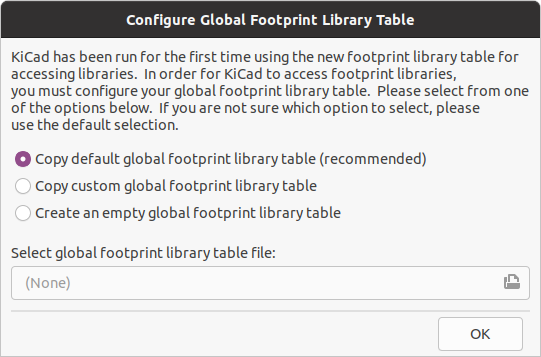
当 PCB 编辑器第一次运行时,如果在 KiCad 配置文件夹中没有找到全局引脚表文件 fp-lib-table,那么 KiCad 将询问如何创建这个文件:
第一个选项是推荐的(复制默认的全局封装库表(推荐))。默认的封装库表包括所有作为 KiCad 的一部分安装的标准封装库。
如果该选项被禁用,KiCad 无法找到默认的全局封装库表。这可能意味着你没有和 KiCad 一起安装标准封装库,或者它们没有被安装在 KiCad 期望找到的地方。在某些系统中,KiCad 库是作为一个单独的软件包安装的。
-
如果你已经安装了标准的 KiCad 封装库并想使用它们,但第一个选项被禁用,选择第二个选项并浏览到安装 KiCad 库的目录中的
fp-lib-table文件。 -
如果你已经有了一个你想使用的自定义封装库表,选择第二个选项并浏览到你的
fp-lib-table文件。 -
如果你想从头开始构建一个新的封装库表,选择第三个选项。
Footprint library management is described in more detail later.
PCB 编辑器的用户界面
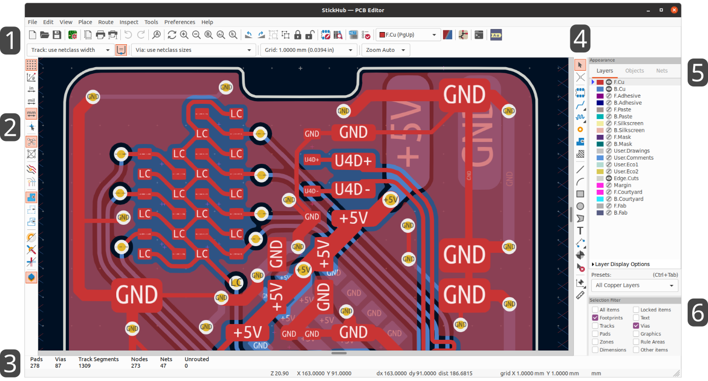
PCB 编辑器的主要用户界面如上图所示,并标明了一些关键元素:
-
顶部工具栏 (文件管理、缩放工具、编辑工具)
-
左侧工具栏 (显示选项)
-
消息面板和状态栏
-
右侧工具栏 (绘图和设计工具)
-
外观面板
-
选择过滤器面板
导航编辑画布
编辑画布是正在设计的板上的视图。您可以平移和缩放到电路板的不同区域,也可以翻转视图以从底部显示电路板。
默认情况下,用鼠标中键或右键拖动会平移画布视图,滚动鼠标滚轮会放大或缩小视图。 你可以在偏好设置中的鼠标和触摸板部分改变这一行为(详见《配置和定制,配置和定制》)。
在顶部的工具栏中,还有其他几个缩放工具可用:
-
 放大视窗的中心。
 -
 从视口中心缩小。
 -
 放大到适合绘图页周围的框架。
 -
 缩放以适应绘图板内的项目。
 -
 允许你画一个方框来确定放大的区域。
光标的当前位置显示在窗口的底部(X 和 Y),还有当前的缩放系数(Z)、光标的相对位置(dx、dy 和 dist)、网格设置和显示单位。
按 Space 可以将相对坐标重置为零。这对于测量两点之间的距离或对齐物体很有用。
快捷键
这个 Ctrl+F1 快捷键显示当前快捷键列表。默认的快捷键列表包括在本手册的 《pcbnew 动作参考,动作参考》部分。
本手册中描述的快捷键使用了标准 PC 键盘上的按键标签。在苹果键盘布局中,使用 Cmd 键来代替 Ctrl,使用 Option 键来代替 Alt。
许多动作默认没有分配快捷键,但可以使用快捷键编辑器(偏好设置 → 偏好设置… → 《偏好控制,快捷键》)分配或重新定义快捷键。
| 通过快捷键可用的许多操作也可在上下文菜单中使用。要访问上下文菜单,请在编辑画布中单击鼠标右键。根据选择的内容或处于活动状态的工具,将提供不同的操作。 |
快捷键存储在 KiCad 的配置目录下的 user.hotkeys 文件中。这个位置是特定于平台的:
-
Windows:
%APPDATA%\kicad\7.0\user.hotkeys -
Linux:
~/.config/kicad/7.0/user.hotkeys -
macOS:
~/Library/Preferences/kicad/7.0/user.hotkeys
KiCad 可以使用快捷键编辑器中的 导入快捷键 按钮从 user.hotkeys 文件中导入快捷键设置。
显示和选择控件
板层
PCB 编辑器中的层代表电路板上的物理铜层,以及用于定义丝印、阻焊和电路板边框等的图形层。 在编辑器中,总有一个层是活动的。 活动层被画在其他层的上面,并且将是分配给新创建的对象的层。 活动层在顶部工具栏的图层选择器下拉框中显示,在外观面板中也被突出显示。 要改变活动层,你可以左键单击外观面板中的层名,使用顶部工具栏中的下拉层选择器,或使用快捷键。 图层可以被隐藏以简化棋盘视图。 你可以隐藏一个层,即使它是活动层。
电路板层的显示顺序
| TODO:写下这一节。 |
外观面板
外观面板提供了管理 PCB 编辑器绘图画布中的对象的可见性、颜色和不透明度的控制。 它有三个标签:层标签包含电路板层的控制,对象标签包含不同类型图形对象的控制,网络标签包含飞线和铜项目的外观控制。
图层控件
在外观面板的图层选项卡中,每个电路板图层都显示了其颜色和可见性状态。 活动图层在色块的左边有一个箭头指示器。 左键点击一个图层来选择它作为活动图层。 左键单击相应的可见性图标,在可见和隐藏之间切换该图层。 双击或中击色块来改变该图层的颜色。
| 必须先在首选参数中创建自定义颜色主题, 然后才能在“外观”面板中更改图层颜色。 |
在图层列表下方是一个包含图层显示选项的可展开面板。第一个设置控制非活动图层的显示方式:正常、暗显或隐藏。层显示模式可用于简化视图并聚焦于单个层。当非活动层显示模式为 "暗显" 或 "隐藏" 时,不能选择非活动层上的项目。您可以使用快捷键 Ctrl+H 快速切换这些显示模式。
翻转电路板视图 将显示电路板,就像从底部看一样(即,绕 Y 轴镜像)。 此选项也可在视图菜单中使用。
| 翻转电路板视图不会更改可视层顺序,活动层将保持在最前面,其他层按正常顺序紧随其后。 |
对象控件
外观面板的 "对象" 选项卡与 "图层" 选项卡类似。 主要区别在于,有些对象没有颜色设置,而四种类型的对象(布线、过孔、焊盘和敷铜)有不透明度控制滑块。 这里的不透明度设置将与图层颜色中设置的任何不透明度相乘。 默认情况下,所有对象都是完全不透明的,除了敷铜,敷铜被设置为半透明,以使通过填充的敷铜更容易看到对象。
图层预设
图层预设存储了哪些图层和对象是可见和隐藏的,以便于调用。 有几个内置的图层预设,您可以保存您自己的自定义预设。 自定义预设存储在一个电路板的工程设置中,因为预设可能是特定于某个电路板的叠加。
要加载一个预设,请从外观面板底部的预设下拉菜单中选择它,或者通过按住 Ctrl 并按 Tab 来使用快速切换器。 一旦快速切换器窗口出现,你可以按 Tab 和 Shift+Tab 来循环浏览可用的预设。 当你放开 Ctrl 键时,高亮显示的预设将被加载。
要保存一个自定义的预设,首先使用可见性控制来选择你希望哪些图层是可见的,然后从预设下拉菜单中选择保存预设…。 给您的预设一个名字,它现在可以通过下拉菜单和快速切换器使用。 要修改一个自定义预设,请遵循相同的过程,并以相同的名称保存修改后的版本,以覆盖现有的版本。 要删除一个自定义预设,从下拉菜单中选择删除预设…选项,并从列表中选择要删除的预设。
网络和网络类控件
外观面板的网络选项卡显示电路板中所有网络和网络类的列表。每个网都有一个可见性控件,用于控制该网在飞线中的可见性。在飞线中隐藏网络不会改变电路板的连接性,也不会影响设计规则检查器;这只是为了使飞线更容易理解。
每个网络和网络类还可以指定一种颜色。默认情况下,此颜色适用于网络 (或网络类中的所有网络) 的飞线。默认情况下,网络没有颜色;这由色样中的棋盘格图案指示。双击或右键单击网络或网络类颜色样本以设置颜色。
| 默认网络类不能分配颜色, 因为该类中的网络将仅使用颜色主题定义的默认飞线最高颜色。 |
您还可以通过外观面板选择并高亮网络和网络类:右击网络或网络类以在菜单中显示这些选项。
网络类列表下面是一个包含网络显示选项的可扩展面板。第一个选项控制如何应用网络颜色。当选择了“所有”时,属于网络或网络类别的所有铜项 (焊盘、布线、过孔和区域) 都将呈现所选的颜色。当选中“飞线”(默认值)时,只有飞线受网络和网络类别颜色的影响。 当选择“没有”时,网络和网络类颜色被忽略。
第二个选项控制如何绘制飞线。“所有图层”表示将在所有未连接的项目之间绘制飞线。“可见层”意味着不会向隐藏层上的项目绘制任何最新的飞线,即使这些项目是未连接的。
选择和选择筛选器
选择编辑画布中的项目是用鼠标左键完成的。 单独点击一个对象将选择该对象,而拖动将执行框选。 从左到右的框选将只选择完全在框内的项目。 从右到左的方框选择将选择任何接触到方框的项目。从左到右的选择框是用黄色画的,光标表示排他性选择,从右到左的选择框是用蓝色画的,光标表示包容性选择。
可以通过在单击或拖动的同时按住快捷键来修改选择操作。单击以选择单个项目时,将应用以下快捷键:
| 修改键 (Windows) | 修改键 (Linux) | 修改键 (macOS) | 选择效果 |
|---|---|---|---|
Ctrl |
Ctrl |
Cmd |
切换选择。注意:Ctrl+点击可以被重新设置为高亮网络。 偏好设置 → PCB 编辑器 → 编辑选项. |
Shift |
Shift |
Shift |
将该项目添加到现有的选择中。 |
Ctrl+Shift |
Ctrl+Shift |
Cmd+Shift |
从现有的选择中删除项目。 |
长点击 |
长点击或 Alt |
长点击或 Option |
从弹出式菜单中清晰选择。 |
拖动以执行选框时,将应用以下快捷键:
| 修改键 (Windows) | 修改键 (Linux) | 修改键 (macOS) | 选择效果 |
|---|---|---|---|
Ctrl |
Ctrl |
Cmd |
切换选择。 |
Shift |
Shift |
Shift - Shift |
将项目添加到现有的选择中。 |
Ctrl+Shift |
Ctrl+Shift |
Cmd+Shift |
从现有选择中删除项目。 |
PCB 编辑器窗口右下角的选择过滤器面板控制哪些类型的对象可以用鼠标选择。 关闭不需要的对象类型的选择,可以使在密集的电路板上选择项目更加容易。 "所有项目" 复选框是打开和关闭其他项目的一个快捷方式。 "锁定的项目" 复选框与其他项目无关,它控制是否可以选择被锁定的项目。 你可以右键单击选择过滤器中的任何对象类型,快速改变过滤器,只允许选择该类型的对象。
当一个连接的铜线项目被选中时,你可以使用右键菜单中的 "扩展选择" 命令或快捷键 U 将选择扩展到同一网络的其他铜线项目。 第一次运行这个命令时,选择将被扩展到最近的焊盘。 第二次,选择将被扩展到所有层上的所有连接项。
选择一个对象会在窗口底部的信息面板上显示该对象的信息。双击一个对象可以打开一个窗口来编辑该对象的属性。
按 Esc 将始终取消当前工具或操作,并返回到选择工具。在选择工具处于活动状态时按 Esc 将清除当前选择。
网络高亮
电气网络(或一组网络)可以在 PCB 编辑器中被高亮显示,以显示该网络是如何在 PCB 上布线的。 通过在 PCB 编辑器中选择要高亮的网络,或者在启用交叉探测高亮时在原理图编辑器中选择相应的网络,可以激活网的高亮(见下文)。 当网络高亮激活时,高亮的网或网将以较亮的颜色显示,所有其他项目将以比正常颜色更暗的颜色显示。
There are three ways to select a net or nets to highlight in the PCB editor: by using the hotkey ` after selecting a copper object, by using the context menu of any copper object, and the context menu of the Nets tab of the Appearance panel. When you press the Highlight Net hotkey, the nets of any selected copper items will be highlighted. If no copper items are selected, the net of the copper item under the editor cursor will be highlighted.
Net highlighting can be cleared by using the Clear Net Highlight action (hotkey ~) or by using the Highlight net tool on an empty region in the schematic. By default, Esc also clears net highlighting, but this can be disabled if desired in Preferences → PCB Editor → Editing Options.
选择一个或多个网络进行高亮时,左侧工具栏上的切换网络高亮显示操作变为启用(也可通过快捷键 Ctrl+` 访问)。此操作将打开或关闭高亮,而无需选择要高亮的新网络。
从原理图交叉探测
KiCad 允许在原理图和 PCB 之间进行双向交叉探测。 有几种不同类型的交叉探测。
选择交叉探测 允许您在原理图中点击一个符号或引脚,在 PCB (如果存在) 中点击相应的封装或焊盘,反之亦然。 默认情况下,交叉探查将导致显示以交叉探查的项目为中心并缩放到合适的位置。 可以在偏好设置对话框的显示选项部分禁用此行为。
高亮交叉探测 允许您同时高亮原理图和 PCB 中的网络。 如果在偏好设置对话框的显示选项部分中启用了选项 "高亮交叉网络", 则在原理图编辑器中高亮某个网络或总线将导致相应的一个或多个网络在 PCB 编辑器中高亮。
左侧工具栏显示控件
左边的工具条提供了改变 PCB 编辑器中项目显示的选项。
|
Turns grid display on/off. Note: by default, hiding the grid will disable grid snapping. This behavior can be changed in the Display Options section of Preferences. |
|
Switch between polar and Cartesian coordinate display in the status bar. |
|
Display/entry of coordinates and dimensions in inches, mils, or millimeters. |
|
Switches between full-screen and small editing cursor (crosshairs). |
|
Turns the ratsnest display on/off. |
|
Switches between straight and curved ratsnest lines. |
|
Switches the non-active layer display mode between Normal and Dim. Note: this button will be highlighted when the non-active layer display mode is either Dim or Hide. In both cases, pressing the button will change the layer display mode to Normal. The Hide mode can only be accessed via the controls in the Appearance Panel or via the hotkey Ctrl+H. |
|
When a net has been selected for highlighting, switches the highlighting on or off. Note: this button will be disabled when no net has been highlighted. To highlight a net, use the hotkey `, right-click any copper object in the net and choose Highlight Net from the Net Tools menu, or right-click the net in the list in the Nets tab of the Appearance panel. |
|
Show zone filled areas. |
|
Show zone outlines only. |
|
Switches display of pads between filled and outline mode. |
|
Switches display of vias between filled and outline mode. |
|
Switches display of tracks between filled and outline mode. |
|
Shows or hides the Appearance and Selection Filter panels on the right side of the editor. |
|
Shows or hides the Properties Manager panel on the left side of the editor. |
创建 PCB
PCB 的基本概念
KiCad 中的印刷电路板通常由代表电子元件及其焊盘的 封装、定义这些焊盘如何彼此连接的 网络、形成每个网络中焊盘之间的铜连接的 布线、过孔 和 填充区 以及定义电路板边缘、丝印标记和任何其他所需信息的各种图形形状组成。
KiCad 通常会将 PCB 上的网络信息与相关的原理图保持同步,但也可以直接在 PCB 编辑器中创建和编辑网络。
性能
KiCad 能够创建多达 32 个铜层、14 个技术层 (丝印、阻焊、元件粘合剂、焊膏等) 和 13 个通用绘图层的印刷电路板。
KiCad 中所有对象的内部测量分辨率为 1 纳米,测量值以 32 位整数存储。 这意味着可以创建最大约 4 米乘 4 米的电路板。
KiCad 目前支持每个工程/原理图一个电路板文件。
从原理图开始
从原理图创建电路板是 KiCad 的推荐工作流程。 当您创建一个新工程时,KiCad 会生成一个与工程名称相同的空板文件。 要在创建原理图后开始设计电路板,只需打开电路板文件。 您可以通过 KiCad 工程管理器,或者点击原理图编辑器中的 "在电路板编辑器中打开 PCB" 按钮来完成。 要将原理图设计信息导入电路板编辑器,包括封装和网络连接,请使用 工具 → 从 PCB 更新原理图… 操作(F8)。你也可以使用顶部工具栏上的 ![]() 图标。
图标。
| 从原理图更新 PCB 是将设计信息从原理图转移到 PCB 的首选方法。在旧版本的 KiCad 中,相应的过程是将网表从原理图编辑器中导出并导入到电路板编辑器中。现在已经没有必要使用网表文件了。 |
关于从 PCB 更新原理图工具的更多信息,请参见手册的《正向批注,正向批注》部分。
从头开始
也可以创建没有匹配原理图的电路板,尽管此工作流程有一些限制,不建议大多数用户使用。为此,您必须独立启动 PCB 编辑器(而不是从 KiCad 工程管理器启动)。在开始设计之前,最好保存电路板文件,该文件还将创建一个工程文件来存储电路板设置。使用 "另存为…" 从文件菜单选择保存电路板文件的位置。将在您选择保存电路板文件的相同位置创建一个同名的工程文件。
电路板设置
在开始您的线路板设计之前,使用电路板设置对话框来配置电路板的基本参数。要打开电路板设置,请单击顶部工具栏中的 ![]() 图标或选择 "电路板设置…" 从文件菜单中选择。
图标或选择 "电路板设置…" 从文件菜单中选择。
配置电路板压层和物理参数
在 "电路板设置" 中,有两个部分用于配置电路板的堆叠和层。 "电路板编辑器层" 部分用于启用或禁用技术层(非铜),如果需要的话,还可以给各层自定义名称。 物理压层部分用于配置铜层的数量,以及铜层和电介质层的物理参数,如厚度和材料类型。介质层、阻焊层和丝印层可以被分配颜色,这将影响电路板在 3D 查看器中的外观。
要配置电路板的压层,从物理压层部分开始:
在左上角设置铜层的数量,然后根据需要输入压层的物理参数。 这些参数可以保留其默认值,但请注意,在导出电路板的 3D 模型时,将使用电路板的厚度值,所以如果你打算使用这个功能,最好确保压层厚度是正确的。
| KiCad 目前仅支持铜层数为偶数的压层。 要创建具有奇数层的设计 (例如,柔性印刷电路板或金属芯印刷电路板), 只需选择下一个最高的偶数,而忽略多余的层。 |
接下来,如果需要,可以使用电路板编辑器层部分重命名或隐藏您不会在设计中使用的非铜层。例如,如果您不打算在设计中使用背面丝印,请取消选中 B.Silkcreen 层旁边的复选框。
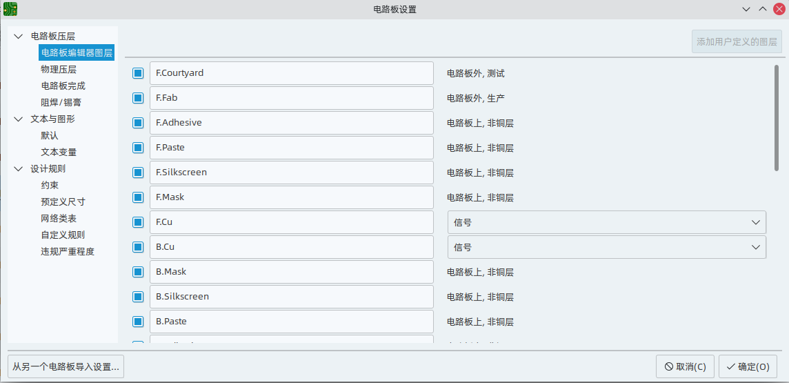
| 在电路板编辑器层部分,可以将铜层指定为信号层、电源层、混合层或跳线层。 本指南仅供用户参考。 无论在此对话框中将类型配置为什么,都可以在任何铜层上布线和敷铜。 |
在电路板编辑器对话框的电路板完成和阻焊/锡膏部分可以找到一些其他的电路板压层设置。电路板完成部分包含用于定义铜电镀和特殊功能 (如镶边或边缘电镀) 的设置。请注意,这些设置目前只影响作为 Gerber 作业文件一部分的电路板属性输出。
阻焊/锡膏部分允许全局调整电路板上焊盘的铜形和阻焊/锡膏形之间的间隙(正或负)。 这些值将被添加到在个别封装或焊盘上设置的任何间隙覆盖。 正的间隙值将导致阻焊层或锡膏开口的形状比铜的形状 更大。 负的间隙值将导致开口比铜的形状 更小。
| 大多数商业 PCB 制造商希望这些值为零,并在 CAM 过程中自行调整阻焊和粘贴开口。 通常最好将这些值保留为默认值零, 除非您自己制作 PCB, 或者您的制造商有具体建议使用不同的值。 |
配置默认文本和图形设置
电路板设置对话框的文本和图形默认值部分可用于配置将用于放置在电路板上的新文本和图形形状的属性。
可以为对话框中显示的六种不同类别的图层配置线粗细、文字大小和文字外观。此外,可以为所有图层配置标注对象的特性。有关标注属性的更多详细信息,请参阅下面的标注部分。
虚线的外观是在 "格式化" 部分控制的。虚线长度 控制虚线的长度,而 间隔长度 控制虚线和圆点之间的间距。虚线和间隔的长度是相对于行宽而言的:间隔长度为 2 意味着是行宽的两倍。
文本替换变量可以在文本变量部分创建。 这些变量允许你将变量名称替换为任何文本字符串。 这种替换发生在变量名称在 ${VARIABLENAME} 的变量替换语法内的任何地方。
例如,您可以创建一个名为 VERSION 的变量,并将文本替换设置为 1.0。 现在,在 PCB 上的任何文本对象中,你可以输入 ${VERSION},KiCad 将替代 1.0。 如果你把替换改为 2.0,每个包括 ${VERSION} 的文本对象都会自动更新。 你也可以混合使用普通文本和变量。 例如,你可以创建一个文本对象,内容为 版本:${VERSION},它将被替换为 版本:1.0。
Text variables can also be created in Schematic Setup. Text variables are project-wide; variables created in the schematic editor are also available in the board editor, and vice versa.
There are also a number of built-in system text variables.
配置设计规则
设计规则控制交互式布线器的行为、覆铜的填充和设计规则检查器。设计规则可以随时修改,但我们建议您在电路板设计过程开始时建立所有已知的设计规则。
约束
基本设计规则是在电路板设置对话框的约束条件部分中配置。 这一部分的约束条件适用于整个板子,应该设置为板子制造商推荐的值。 这里设置的任何最小值都是一个 绝对(absolute) 的最小值,不能被更具体的设计规则所覆盖。 例如,如果你需要电路板的一部分的铜间隙为 0.2mm,其余部分为 0.3mm,你必须在约束条件部分输入 0.2mm 的最小铜间隙,并使用网络类或自定义规则来设置较大的 0.3mm 间隙。
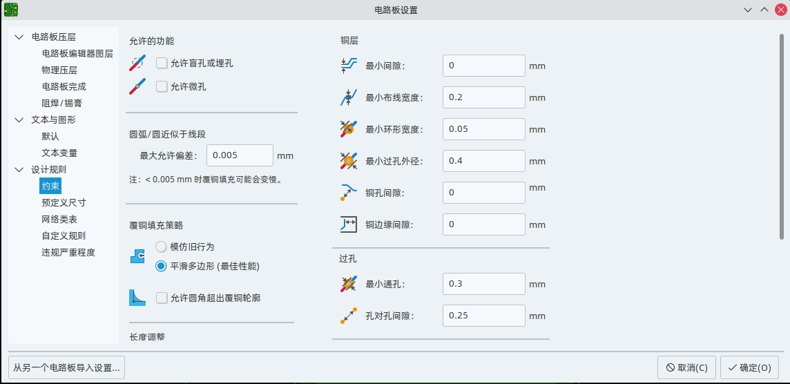
除了设置最小间隙外,还可以在此处配置许多功能:
| 设置 | 说明 |
|---|---|
弧/圆的近似线段 |
在某些情况下,KiCad 必须使用一系列的直线段来近似圆的形状,如圆弧和圆形的形状。 此设置控制了这种近似允许的最大误差:换句话说,这些线段上的一个点与圆弧或圆形的真实形状之间的最大距离。 将此设置为比默认值 0.005 毫米更低的数字将导致更平滑的形状,但在较大的电路板上可能会非常慢。默认值通常会导致圆弧的近似误差,由于制造公差的原因,在制造出来的电路板上是检测不到的。 |
敷铜可以在敷铜属性对话框中添加圆角(圆角) |
默认情况下,在敷铜边框外不允许有敷铜,包括圆角。 这实际上意味着,即使配置了圆角,敷铜边框的内角也不会被圆角化。通过启用此设置,敷铜边框的内角将被拉丝,即使这导致边框的铜延伸到敷铜边框之外。 |
最小散热辐条数 |
这设置了连接焊盘和敷铜的最小可接受的散热辐条数量。如果违反了这个约束,将会产生 DRC 违规。 |
在布线长度计算中包压层高度 |
默认情况下,压层的高度被用来计算从一层到另一层通过通孔的布线的额外长度。 这种计算依赖于电路板压层高度的正确配置。 在某些情况下,最好是忽略过孔的高度,只计算布线的长度,假设过孔不增加长度。 禁用此设置将从布线长度计算中排除过孔长度。 |
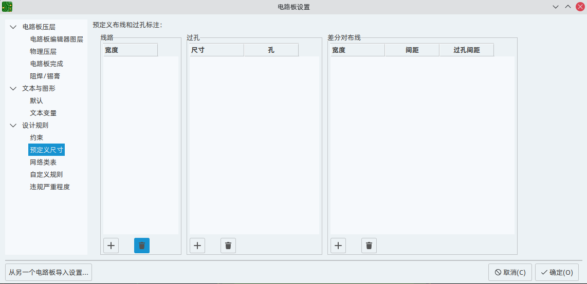
预定义大小
预定义的尺寸部分允许你定义你希望在布线时可用的布线和过孔尺寸。 网络类可以用来定义不同网络中的布线和过孔的默认尺寸(见下文),但是在这个部分定义一个尺寸列表,可以让你在布线的时候逐步了解这些尺寸。 例如,你可能希望电路板上的默认布线宽度是 0.2 mm,但对于一些承载更多电流的部分使用 0.3 mm,而对于一些空间有限的部分使用 0.15 mm。 您可以在电路板设置对话框中定义这些布线的宽度,然后在布线时在它们之间切换。
网络类
The Net Classes section allows you to configure routing and clearance rules for different classes of nets. In KiCad, each net is part of exactly one net class. If you do not add a net to a specific class, it will be part of the Default class, which always exists. Net classes may be created and edited in either the Schematic or Board Setup dialogs.
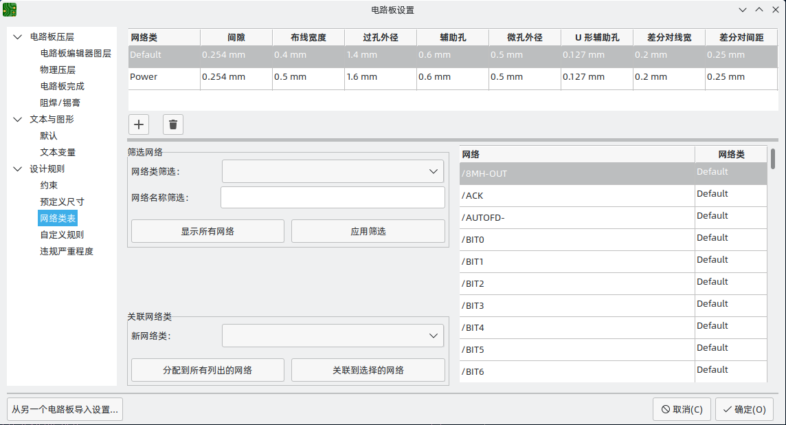
网络类部分的上部有一个表格,显示了设计中的网络类和适用于每个网络类的设计规则。 每个类别都有铜的间隙、布线宽度、过孔尺寸和差分对尺寸的值。 这些值将在创建布线和过孔时使用,除非有更具体的规则覆盖它们(见下面的自定义规则)。
任何规则都不能覆盖电路板设置的约束条件部分中设置的最小值。
例如,如果您将网络类间距设置为 0.1 mm,但约束条件部分中的最小间距设置为 0.2 mm,
则该类网络的间距将为 0.2 mm。
|
当 PCB 编辑器中的布线宽度和过孔尺寸控制设置为 "使用网络类值" 时,就会使用为每个网络类定义的布线宽度和过孔尺寸。 这些宽度和尺寸被认为是该网络类的默认或最佳尺寸。 它们不是最小或最大值。 手动将布线宽度或过孔尺寸改为与网络类部分定义的不同的值,不会导致违反 DRC。 要将布线宽度或过孔大小限制在特定的值,请使用自定义规则。
The lower portion of the Net Classes section lists pattern-based netclass assignments. Working with pattern-based netclass assignments is explained in the Schematic Editor documentation; pattern-based assignments can be edited in either the Board or Schematic Setup windows.
Note that pattern-based assignments can be created directly from the PCB editing canvas by right clicking a copper track or zone and clicking Assign netclass…. Netclasses can also be assigned in the schematic using netclass directives or labels instead of pattern-based assignments.
自定义规则
自定义规则部分包含一个文本编辑器,用于使用自定义规则语言创建设计规则。 自定义规则用于创建基本约束或网络类设置没有涵盖的特定设计规则检查。
只有在自定义规则定义中没有错误时,才会应用自定义规则。 在关闭电路板设置之前,使用检查规则语法器按钮来测试定义并修复任何问题。
请参阅高级主题一章中的自定义设计规则,了解关于自定义规则语言的更多信息以及规则实例。
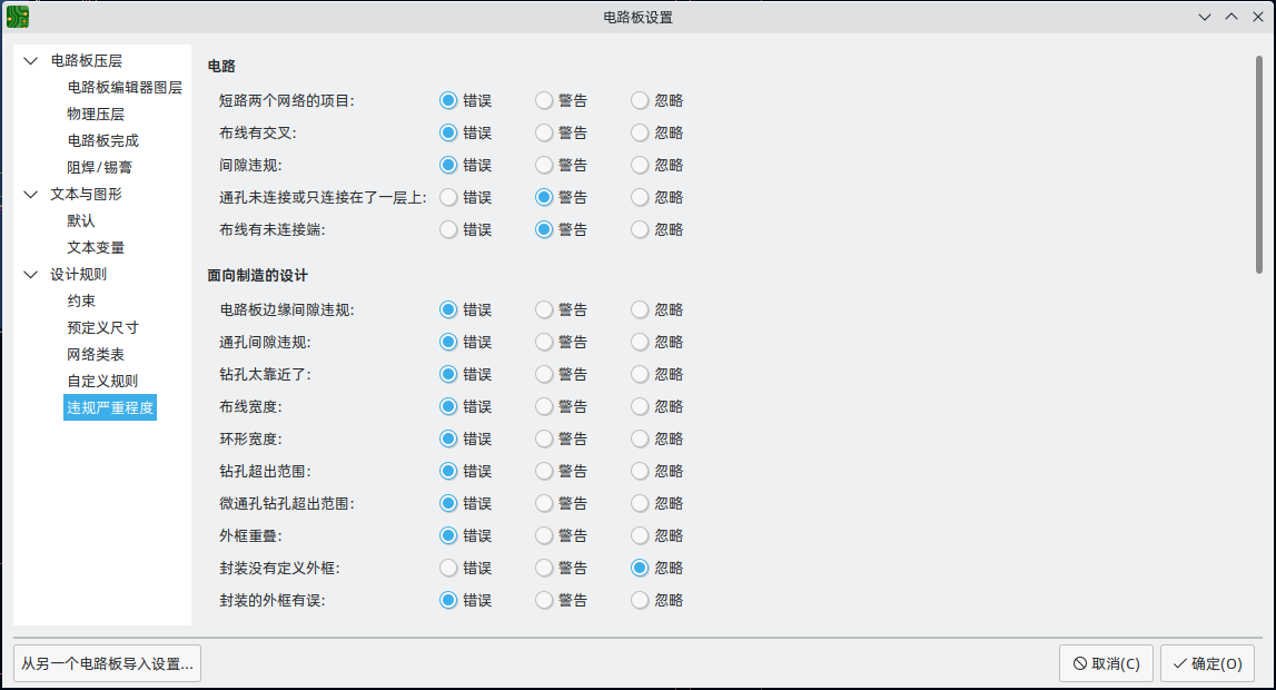
违规严重程度
违规严重性部分允许你配置每种设计规则检查的严重性。 每条规则可以被设置为创建一个错误标记、一个警告标记或没有标记(忽略)。
| 在设计规则检查器中可能会忽略个别规则违规。 在违规程度部分中将规则设置为忽略将完全禁用相应的设计规则检查。 请谨慎使用此设置。 |
正在导入设置
您可以从现有电路板导入部分或全部电路板设置。此技术可用于创建具有您想要在多个设计上使用的设置的 "模板" 电路板,然后将这些设置从模板电路板导入到每个新电路板中,而不是手动输入。
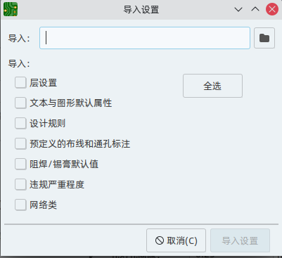
要导入设置,请点击电路板设置对话框底部的 从另一个电路板导入设置… 按钮,然后选择您要导入的 kicad_pcb 文件。 选择你想导入的设置,当前的设置将被选定的板子的值覆盖。
编辑电路板
放置和绘制操作
放置和绘图工具位于右边的工具栏中。 当一个工具被激活时,它将一直处于激活状态,直到选择了一个不同的工具或用 Esc 键取消该工具。 当任何其他工具被取消时,选择工具总是被激活。
某些工具栏按钮在调色板中有多个可用工具。这些工具由按钮右下角的小箭头表示:
要显示调色板,你可以在工具上点击并按住鼠标按钮,或者点击并拖动鼠标。 调色板关闭时将显示最近使用的工具。
|
Selection tool (the default tool). |
|
Local ratsnest tool: when the board ratsnest is hidden, selecting footprints with this tool will show the ratsnest for the selected footprint only. Selecting the same footprint again will hide its ratsnest. The local ratsnest setting for each footprint will remain in effect even after the local ratsnest tool is no longer active. |
|
Footprint placement tool: click on the board to open the footprint chooser, then click again after choosing a footprint to confirm its location. |
|
Route tracks / route differential pairs: These tools activate the interactive router and allow placing tracks and vias. The interactive router is described in more detail in the Routing Tracks section below. |
|
Tune length: These tools allow you to tune the length of single tracks or the length or skew of differential pairs, after they have been routed. See the Routing Tracks section for details. |
|
Add vias: allows placing vias without routing tracks. Vias placed on top of tracks using this tool will take on the net of the closest track segment and will become part of that track (the via net will be updated if the pads connected to the tracks are updated). Vias placed anywhere else will take on the net of a copper zone at that location, if one exists. These vias will not automatically take on a new net if the net of the copper zone is changed. |
|
Add filled zone: Click to set the start point of a zone, then configure its properties before drawing the rest of the zone outline. Zone properties are described in more detail below. |
|
Add rule area: Rule areas, formerly known as keepouts, can restrict the placement of items and the filling of zones and can also define named areas to apply specific custom design rules to. |
|
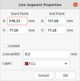
Draw lines. Note: Lines are graphical objects and are not the same as tracks placed with the Route Tracks tool. Graphical objects cannot be assigned to a net. |
|
Draw arcs: pick the center point of the arc, then the start and end points. By right clicking this button, you can change the arc editing mode between a mode that maintains the existing arc center and a mode that maintains the arc radius. |
|
Draw rectangles. Rectangles can be filled or outlines. |
|
Draw circles. Circles can be filled or outlines. |
|
Draw graphical polygons. Polygons can be filled or outlined. Note: Filled graphical polygons are not the same as filled zones: graphical polygons cannot be assigned to a net and will not keep clearance from other items. |
|
Add bitmap image. |
|
Add text. |
|
Add a textbox. |
|
Add dimensions. Dimension types are described in more detail below. |
|
Deletion tool: click objects to delete them. |
|
Set drill/place origin (used for fabrication outputs) or grid origin. |
|
Interactively measure the distance between two points. |
捕捉
移动、拖动和绘制电路板元素时,栅格、焊盘和其他元素可以具有捕捉点,具体取决于用户偏好设置中的设置。在复杂的设计中,捕捉点可能离得太近,这会使当前的工具操作变得困难。使用下表中的快捷键可以在移动鼠标时禁用栅格和对象捕捉。
| 快捷键 | 效果 |
|---|---|
Ctrl |
关闭网格捕捉。 |
Shift |
关闭对象捕捉。 |
编辑对象属性
所有对象都有可在对话框中编辑的属性。 使用快捷键 E 或从右键菜单中选择属性来编辑所选项目的属性。 只有当你选择的所有项目都是同一类型时,你才能打开属性对话框。 要想一次编辑不同类型的项目的属性,请参阅下面关于批量编辑工具的章节。
在属性对话框中,任何包含数字值的字段也可以接受一个基本的数学表达式,从而得到一个数字值。 例如,一个尺寸可以被输入为 2 * 2mm,结果是 4mm 的值。 支持基本算术运算符以及用于定义运算顺序的圆括号。
使用封装
Adding footprints to the board
Footprints are automatically added to the board when the PCB is updated from the schematic. The footprint associated with each schematic symbol is added to the board if it is not already present, and each footprint pad is associated with the corresponding symbol pin’s net. Symbol pins are matched to footprint pads by pin/pad number.
When footprints are added to the board after an update from the schematic, they are grouped by schematic sheet and by geographical location in the schematic. They are initially attached to the cursor; you can place them by clicking in the desired location.
You can also add footprints to the board manually using the Add Footprint tool (A or the ![]() button). Note that footprints added in this way will not be automatically associated with a symbol or have nets assigned to their pads, and subsequent updates from the schematic will remove these unassociated footprints unless the footprint is locked or the Delete footprints with no symbols option is unchecked in the Update PCB From Schematic dialog. For these reasons, it is usually recommended to avoid manually adding footprints to the board. Manually adding footprints is necessary for PCB-only workflows, and can also be useful for adding logos or other footprints that do not need a corresponding schematic symbol.
button). Note that footprints added in this way will not be automatically associated with a symbol or have nets assigned to their pads, and subsequent updates from the schematic will remove these unassociated footprints unless the footprint is locked or the Delete footprints with no symbols option is unchecked in the Update PCB From Schematic dialog. For these reasons, it is usually recommended to avoid manually adding footprints to the board. Manually adding footprints is necessary for PCB-only workflows, and can also be useful for adding logos or other footprints that do not need a corresponding schematic symbol.
Placing and moving footprints
Once footprints have been added to the board, you can reposition them in many ways.
The Move command (M) moves a footprint or a selection of footprints, ignoring any connected track segments that are not selected. No DRC checking is done when moving footprints with the Move command.
There is a reference point for the move operation, which is the point in the footprint which attaches to the cursor and therefore the point in the footprint that snaps to the grid and to other objects. The reference point during a move is determined by the location of the cursor when the Move command is initiated. If the cursor is over a pad, the pad’s center will be used as the reference point. If the cursor is not over a pad, the footprint’s anchor (coordinate origin point) will be used. To select an arbitrary snapping point, you can use the Move With Reference command instead of the regular Move command (right click → Positioning Tools → Move with Reference). After initiating the command, click on the desired reference point; KiCad will then begin the move with that point as the reference.
You can also use the Drag command (D) to move the selected footprint using the interactive router, maintaining all track connections to the footprint. Dragging footprints behaves like the Highlight Collisions router mode: obstacles will not be avoided or shoved, only highlighted. Only one footprint at a time can be dragged.
Flip a footprint to the opposite side of the board with the F hotkey. Any parts of the footprint on a front layer will be swapped to the corresponding back layer, and vice versa.
Rotate a footprint counter-clockwise using the R hotkey, or clockwise using Shift+R. By default, footprints are rotated by 90 degrees every time the rotate command is used, but you can configure the rotation angle step in Preferences → PCB Editor → Editing Options.
You can directly set a footprint’s exact absolute position, rotation angle, and PCB side using either the Footprint Properties dialog or the Properties panel.
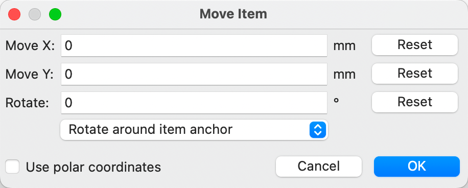
To reposition a footprint relative to its current position, use the Move Exactly tool (Shift+M). The dialog lets you specify an X and Y translation, as well as a rotation, that will be applied to the footprint. The rotation can be performed relative to either the footprint’s anchor, the local coordinate origin, or the drill/place origin. You can also use polar coordinates instead of Cartesian coordinates.
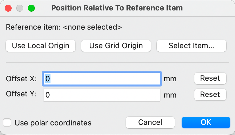
To position a footprint relative to another object, you can use the Position Relative tool (Shift+P). With this tool, you select a reference point for the move, which can be the local origin, the grid origin, or another arbitrary point, such as a pad in another footprint. The selected footprint is moved to the specified offset from the reference point.
You can swap the position of two selected footprints using the Swap command (Shift+S). The first footprint is assigned the location, rotation, and board side of the second footprint, and vice versa. If there are more than two footprints selected, the locations are cycled: the last footprint gets the position of the first footprint, the first footprint gets the location of the second, and so on.
There are several convenience features that make it easier to find, select, and move specific footprints or footprints related to another footprint.
The Get and Move Footprint command (T) prompts you to choose a footprint from a list or by typing a reference designator. KiCad then attaches the chosen footprint to your cursor for a move operation.
There are two commands to select other footprints that need to be connected to the selected footprint but don’t yet have routed connections. The Select All Unconnected Footprints command (O) selects all footprints that have ratsnest lines to the currently selected footprints. The command can be executed repeatedly to further expand the selection based on the newly selected items. The Grab Nearest Unconnected Footprint command (Shift+O) selects the closest footprint with ratsnest lines to the currently selected footprint, and additionally begins to move it. If there are multiple footprints initially selected, the command will act like the Move Individually command described below, individually moving the closest unconnected footprint for each of the initially selected footprints.
You can select footprints based on their schematic sheet using the right click → Select → Items in Same Hierarchical Sheet command, which selects all other footprints that are in the same schematic sheet as the originally selected footprint.
If you want to move multiple selected footprints in sequence, use the Move Individually command (Ctrl+M). After triggering the command, KiCad will begin moving the first selected footprint. After you click to place the footprint, KiCad will immediately start moving the next footprint, in the same order that you selected the footprints. You can skip moving a footprint by pressing Tab, commit the current move and skip any remaining moves by double-clicking, or cancel all moves (including those already completed) by pressing Esc.
If you want to move a collection of footprints at once into one area, the Pack and Move Footprints command (P) closely packs the selected footprints together and moves them as a block.
| Move Individually and Pack and Move Footprints are useful in combination with other selection convenience features, such as cross-selection from the schematic or the advanced footprint selection features described above. For example, you could select a group of bypass capacitors in the Schematic Editor, switch to the PCB Editor where the corresponding footprints are now selected, and then use Move Individually to quickly place all of the bypass capacitor footprints close to their respective ICs. Alternatively, you could use one of the other selection tools, such as Select All Unconnected Footprints, to select many footprints from all over the board, then use Pack and Move Footprints to quickly put them all into a small area. |
Finally, KiCad can automatically place footprints onto the board. The auto-place function attempts to optimally place footprints to simplify ratsnest connections to other footprints. You can auto-place the selected footprints with Place → Auto-Place Footprints → Place Selected Footprints, or auto-place all footprints outside of the board outline with Place → Auto-Place Footprints → Place Off-Board Footprints.
封装属性
| This section of the KiCad documentation has not yet been written. We appreciate your patience as our small team of volunteer documentation writers work to update and expand the documentation. |
Editing Footprints
| This section of the KiCad documentation has not yet been written. We appreciate your patience as our small team of volunteer documentation writers work to update and expand the documentation. |
使用焊盘
在将封装放置在电路板上之后,可以检查和编辑封装的每个单独的焊盘的属性。 换句话说,如果库中的封装设计不合适,就可以在电路板上封装的特定实例中覆盖单个封装焊盘的设计。 例如,你可能希望为一个需要在特定设计中保持不焊接的焊盘去除焊膏孔,或者你可能希望移动一个轴向引线电阻的通孔焊盘的位置,以适应特定的设计。
| 默认情况下,所有封装焊盘的位置都被锁定,因此可以编辑焊盘属性,但不能移动焊盘相对于封装其他部分的位置。 焊盘可以被解锁以允许自由移动,这对某些应用很有用(如具有不同引线位置的通孔封装),但通常不建议用于表面贴装封装。 |
当一个焊盘被选中时,焊盘属性对话框将通过上下文菜单或默认的快捷键E打开。 请注意,KiCad 认为如果你在焊盘附近点击,你可能是想选择整个封装而不是单个焊盘。 要选择单个焊盘,请确保在焊盘区域内点击,或者关闭选择过滤器中的 "封装" 设置(并确保 "焊盘" 设置打开),以防止意外地选择整个封装而不是特定的焊盘。
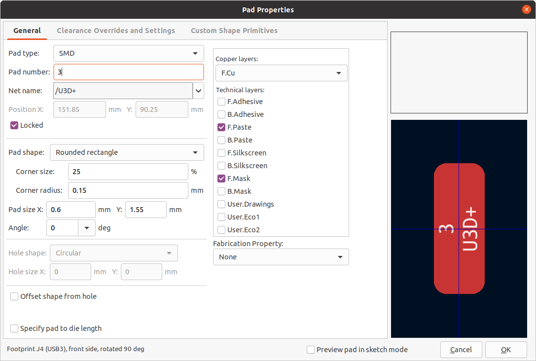
焊盘属性对话框的常规选项卡显示了焊盘的物理属性,包括它的几何、形状和层设置。
焊盘类型: 此设置控制焊盘的哪些功能被启用。
SMD 焊盘是电连接的,没有孔。 换句话说,它们存在于一个单一的铜层上。
通孔 焊盘是电气连接的,有一个电镀孔。 孔存在于每一层,而铜焊盘存在于多层(见下文 铜层 设置)。
板边连接器 焊盘是允许与 Edge.Cuts 层上的电路板边框重叠的 SMD 焊盘。
NPTH,机械 焊盘是没有电镀的通孔,不具有电气连接。
SMD 光圈 焊盘是没有孔和没有电连接的焊盘。 这些可用于在技术层上添加特定的设计,例如锡膏或焊接掩模孔径。(SMD 定位孔)
铜层 设置控制哪些铜层将有一个与焊盘相关的形状。
对于 SMD 焊盘,选项是 F.Cu 或 B.Cu,控制焊盘是在电路板的前面还是后面 相对于封装的位置。 换句话说,如果一个焊盘在其属性中被设置为存在于 B.Cu 上,而封装被翻转到电路板的背面,该焊盘现在将存在于 F.Cu 上,因为它也被翻转了。
对于通孔焊盘,有可能从焊盘与其他铜(布线或填充区)没有电气连接的铜层中移除焊盘形状。 将铜层设置为 连接层 将从任何未连接层移除焊盘形状,而设置为 F.Cu、B.Cu 和连接层 将从任何内部未连接层移除焊盘形状。 这在密集的电路板设计中很有用,可以增加内部层的可布线面积。
技术层 复选框控制哪些技术层会有一个与焊盘形状相同的孔径。 默认情况下,焊盘在粘贴层和屏蔽层上的孔径与铜层相匹配。
| 在当前版本的 KiCad 中,不可能在不同的铜层上定义不同的焊盘形状或尺寸。 |
指定焊盘到模具的长度: 此设置允许将一个长度与此焊盘相关联,该长度将被布线长度调整工具和网络检测器添加到布线的长度中。这可以用来指定内部键合线的长度,以便更准确地进行长度匹配,或者在其他情况下,网络的电气长度长于电路板上的布线的长度。
出现在任何技术层上的孔径将具有与铜层上的焊盘形状相同的形状和尺寸。 在 PCB 制造过程中,制造商经常会改变掩膜和浆料孔径相对于铜焊盘尺寸的相对尺寸,但由于这种尺寸变化是特定于制造过程的,大多数制造商希望在提供设计数据时将孔径设置为与铜焊盘相同的尺寸。 对于需要在设计数据中加大或缩小技术层孔径的特定情况,你可以使用 "覆盖" 标签中的设置。
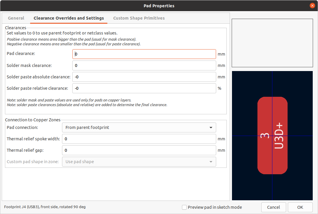
焊盘间隙 控制焊盘与不同网络上的任何铜形状(布线、通孔、焊盘、区域)之间的最小间隙。 这个值通常被设置为 0,这将导致焊盘的间隙被继承自封装上设置的任何间隙覆盖,或者电路板的设计规则和网络类规则(如果封装的间隙也被设置为 0)。
焊接掩模间隙 控制 F.Mask 和 B.Mask 层上的焊盘形状和孔径形状之间的尺寸差异。 一个正数意味着焊接掩模孔径将大于铜的形状。 这个数字是一个适用于所有方向的膨胀。 例如,这里的 0.1mm 值将导致阻焊孔径膨胀 0.1mm,这意味着在焊盘的所有侧面将有 0.1mm 的边界,当沿给定轴线测量时,阻焊开口将比焊盘宽 0.2mm。
焊膏绝对间隙 控制 F.Paste 和 B.Paste 层上焊盘形状和孔径形状之间的尺寸差异。 它的行为在其他方面与 焊膏间隙 设置的行为相同。
焊膏相对间隙 允许将焊膏间隙值设置为焊盘尺寸的百分比,而不是绝对距离值。 如果同时指定了相对间隙和绝对间隙,它们将被加在一起以确定锡膏孔径的大小。
"覆盖" 选项卡还可以控制焊盘如何连接到任何与之重叠并共享其网络的铜区。
焊盘连接 控制焊盘是否与区段有实心的、散热的或无连接。 与其他覆盖项一样,这个覆盖项可以为单个垫块或整个封装设置。 这个控制的默认设置是 从父系封装,而默认的封装设置是使用区段属性中指定的连接模式。
散热辐条宽度 控制区段连接模式为散热时产生的辐条的宽度。
散热间隙 控制散热条的长度,或焊盘的形状和区域的填充铜面积之间的间隙。
区域内的自定义焊盘形状 当焊盘使用自定义形状而不是默认形状之一时,控制区域填充器的行为。 这可以用来在使用散热条和自定义焊盘形状时实现不同的结果。
使用区域
铜区,有时也被其他 EDA 工具称为铜岛或填充,是分配给一个特定网络的实心或多边形的铜区,自动保持与其他铜对象的间隙。 铜区通常用于填充板层(或板层的一部分)上的所有自由空间,以创建接地和电源平面,承载大电流,或提供屏蔽。
| 一些 EDA 工具有单独的工具用于创建 "放置层" 和在信号层上创建铜区。 在 KiCad 中,铜区工具被用于这两种应用。 |
区域是由一个多边形的 边框 来定义的,它定义了填充铜区的最大范围。 这个边框并不代表物理铜,也不会出现在导出的制造数据中。 每次修改边框或边框内的任何对象时,该区的实际铜区必须被 填充。 填充过程可以在单个区上运行,也可以在电路板的所有区上运行(默认快捷键 B)。 区域可以 不填充(默认快捷键 Ctrl+B),以提高性能并减少编辑大板时的视觉混乱。
| By default, zone filling is a manual process rather than occurring every time an object changes that would result in a change to the zone copper. This is because zone filling can be a slow process on older computers or very large designs. It is important to make sure zone fills are up-to-date before generating outputs. KiCad will check that zones have been updated and warn you before generating outputs or running DRC when zones have not yet been refilled. You can optionally enable automatic zone-filling in the Preferences dialog (PCB Editor → Editing Options → Miscellaneous → Auto-refill zones). |
To draw a zone, click the Add Filled Zone tool (![]() ) on the right toolbar, or use default hotkey Ctrl+Shift+Z. Click to choose the first point of the zone outline. The Zone Properties dialog will appear, allowing you to choose the zone net and other properties. These properties may be edited at any time, so it is not critical to choose them all correctly at first. Accept the dialog and continue placing points to define the zone outline. To finish the zone, double-click to set the last point. Zone outline points may be modified like graphic polygons, by dragging the square handles to move a corner or dragging the circular handles to move an edge. To edit the zone’s properties, use hotkey E or select Properties from the context menu.
) on the right toolbar, or use default hotkey Ctrl+Shift+Z. Click to choose the first point of the zone outline. The Zone Properties dialog will appear, allowing you to choose the zone net and other properties. These properties may be edited at any time, so it is not critical to choose them all correctly at first. Accept the dialog and continue placing points to define the zone outline. To finish the zone, double-click to set the last point. Zone outline points may be modified like graphic polygons, by dragging the square handles to move a corner or dragging the circular handles to move an edge. To edit the zone’s properties, use hotkey E or select Properties from the context menu.
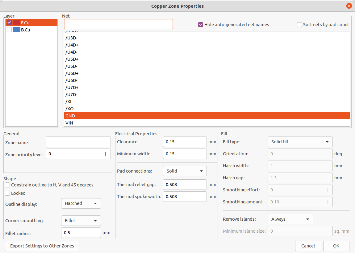
层: 一个区域对象可以在一个或多个铜层上创建填充铜。 勾选每个铜层旁边的方框,这个区域边框应该在这些铜层上填充。 每个层上的铜将被独立地填充,但所有层将共享同一个网络。
网络: 选择该区铜区应连接的电气网络。 可以创建没有网络分配的区域。 没有网络的区域将与任何网络上的任何铜对象保持间隙。
区域名 可以用来给一个区域指定一个特定的名称。 这个名字可以用来在自定义的 DRC 规则中指代该区域。
Zone priority level determines the order in which multiple zones on a single layer are filled. The highest priority level zone on a given layer will be filled first. Lower-priority zones will keep clearance to the filled areas of higher-priority zones. Two zones on the same layer with the same priority level will overlap (short-circuit) with each other, unless they are assigned different nets. When two zone outlines with the same priority and different nets touch, one zone will maintain clearance to the other so that they don’t short.
限制边框为 H、V 和 45 度 控制区域边框绘制工具的 初始 行为。 当这个选项被启用时,区域边框将被限制在 45 度的角度。 请注意,在创建了区域边框之后,这个选项就没有作用了。 边框点在创建后可以自由修改。
锁定 控制区域边框对象是否被锁定。 被锁定的对象不能被操作或移动,也不能被选择,除非在选择过滤器面板中启用 锁定的项目 选项。
边框显示 控制区域边框在屏幕上的绘制方式。 在 直线 模式下,只绘制边框的边界线。 在 阴影 模式下,阴影线会在边框边界的内侧绘制一小段距离,以使区段边框更加明显。 在 完全阴影 模式下,阴影线被绘制在整个区域边框的内部。
拐角平滑 控制边框拐角处的填充铜区的行为。拐角可以通过倒角或圆角来平滑,如果平滑被禁用,也可以一直延伸到边框的拐角。
| 默认情况下,倒角和圆角不会被添加到区域边框的内角,因为这将导致填充的铜延伸到边框之外。 如果需要光滑的内角,请在电路板设置对话框的约束部分启用 允许区域边框外的圆角 选项。 |
间隙 控制该区域的填充区域与其他铜质物体保持的最小间隙。 请注意,如果两个间隙值有冲突,将使用较大的间隙值。 例如,如果一个区被设置为使用 0.2 毫米的间隙,但其网络类被设置为使用 0.3 毫米的间隙,结果将是 0.3 毫米的间隙。
最小宽度 控制在该区域内产生的铜间隙的最小尺寸。 任何低于这个最小宽度的铜区都会在填充过程中被移除。
焊盘连接 控制填充区与同一网络上的封装焊盘的连接方式。 实心 连接将导致铜完全重叠在焊盘上。散热焊盘 将导致小铜辐条连接焊盘和铜区的其余部分,增加焊盘和区的其余部分之间的热阻。 这对手工焊接很有用。 对 PTH 的散热焊盘 将对电镀通孔焊盘应用散热焊盘,并对表面贴装焊盘使用固体连接。 无 将导致该区不连接到同一网络上的任何焊盘。
散热间隙 控制任何焊盘和铜区之间保持的距离,当焊盘连接模式被设置为产生散热。
散热宽度 控制 "辐条" 的宽度,即连接焊盘和其他铜区的短铜段。
填充类型 控制铜区的填充方式:默认为 实心填充,这将导致铜填充在区域边框内的所有可用空间。 该区域也可以被设置为 填充图案,这将使该区域充满含铜量较少的图案。
方向 控制孵化图案线的角度。 一个 0 度的方向将导致孵化图案使用水平和垂直的线条。
填充宽度控制填充图案中每条线的宽度。
填充间隙 控制填充图案中每条线之间的距离。
平滑效果 控制应用于填充图案的平滑风格。 0 的值将导致无平滑,3 的值将导致最精细的平滑。 更高的值将导致更长的处理时间和更大的 Gerber 文件。
平滑量 是一个比率,控制平滑倒角或圆角的大小,当 平滑效果 被设置为 0 以外的值时,会产生平滑倒角。
移除孤岛 控制初始区域填充后孤立的铜区(也称为孤岛)的行为。 当设置为 总是 时,区域内的孤立区域会被移除。当设置为 从不 时,孤立区域会被搁置,并会导致铜区不与网络的其他部分连接。 当设置为 低于区域限制时,可以指定一个 **最小的孤岛尺寸,低于这个阈值的孤岛将被删除。
| Regardless of the remove islands setting, islands are never removed from zones that are electrically unconnected. In other words, islands are only removed from zones that have at least one electrical connection. |
图形对象
图形对象 (直线、圆弧、矩形、圆、多边形和文本)可以存在于任何图层上,但不能分配给网络。矩形、圆和多边形可以在其属性对话框中设置为填充或边框。线宽属性将控制边框的宽度,即使是填充形状也是如此。填充形状的线宽可以设置为 "0" 以禁用边框。
正在创建图形形状
The right toolbar can be used to create lines (![]() , default hotkey Ctrl+Shift+L), arcs (
, default hotkey Ctrl+Shift+L), arcs (![]() , default hotkey Ctrl+Shift+A), rectangles (
, default hotkey Ctrl+Shift+A), rectangles (![]() ), circles (
), circles (![]() , default hotkey Ctrl+Shift+C), and polygons (
, default hotkey Ctrl+Shift+C), and polygons (![]() , default hotkey Ctrl+Shift+P).
, default hotkey Ctrl+Shift+P).
矩形、圆形和多边形可以是填充形状或边框。 线宽 选项控制边框的宽度。 边框宽度在图形对象的 "理想" 形状的两边延伸。 例如,一个被定义为半径为 2 毫米、线宽为 0.2 毫米的图形圆将由一个外半径为 2.2 毫米、内半径为 1.8 毫米的圆环组成。 如果启用了 填充形状 选项,并且线宽被设置为 0,该形状将是一个半径为 2 毫米的填充圆。
Arcs have two editing modes, which are selectable in Preferences → PCB Editor → Editing Options or by right clicking the ![]() button on the right toolbar. The first mode (keep arc center, adjust radius) maintains the position of the arc center as as the arc endpoints or midpoint are dragged, changing the radius as necessary. The second mode (keep arc endpoints or direction of starting point) maintains the position of the arc endpoints and the arc’s direction of curvature as the midpoint or center are dragged.
button on the right toolbar. The first mode (keep arc center, adjust radius) maintains the position of the arc center as as the arc endpoints or midpoint are dragged, changing the radius as necessary. The second mode (keep arc endpoints or direction of starting point) maintains the position of the arc endpoints and the arc’s direction of curvature as the midpoint or center are dragged.
正在创建文本对象
图形文字可以通过使用右侧工具栏的(![]() )图标或键盘快捷键 Ctrl+Shift+T 来放置。 点击来放置文本原点,然后在出现的对话框中编辑文本及其属性:
)图标或键盘快捷键 Ctrl+Shift+T 来放置。 点击来放置文本原点,然后在出现的对话框中编辑文本及其属性:
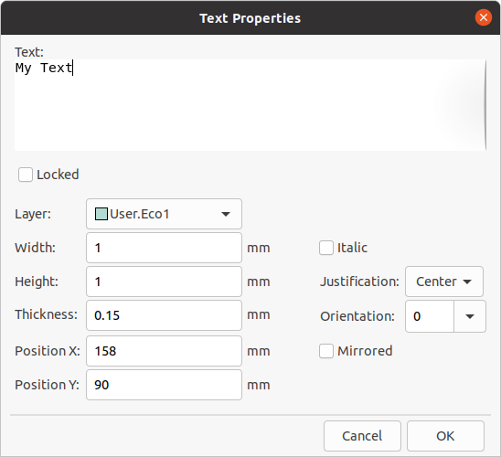
文字可以放在任何层上,但要注意,铜层上的文字不能与网络关联,不能与布线或焊盘形成连接。 铜区将填充在文字对象的矩形边界框周围。
Text supports markup for superscripts, subscripts, overbars, evaluating project variables, and accessing symbol field values.
| Feature | Markup Syntax | Result |
|---|---|---|
Superscript |
|
textsuperscript |
Subscript |
|
textsubscript |
Overbar |
|
text |
|
variable_value |
|
|
field_value of symbol refdes |
| Variables must be defined in Board Setup before they can be used. There are also a number of built-in text variables. |
电路板边框 (边缘切割)
KiCad 使用 Edge.Cuts 层上的图形对象来定义电路板的边框。 该边框必须是一个连续(封闭)的形状,但可以由不同类型的图形对象组成,如线和弧,或者是一个单一的对象,如矩形或多边形。 如果没有定义电路板的边框,或者电路板的边框无效,那么一些功能,如 3D 查看器和一些设计规则的检查将无法发挥作用。
批量编辑文本和图形
文本和图形的属性可以通过 编辑文本和图形属性 对话框(工具 → 编辑文本和图形属性…)来进行批量编辑。
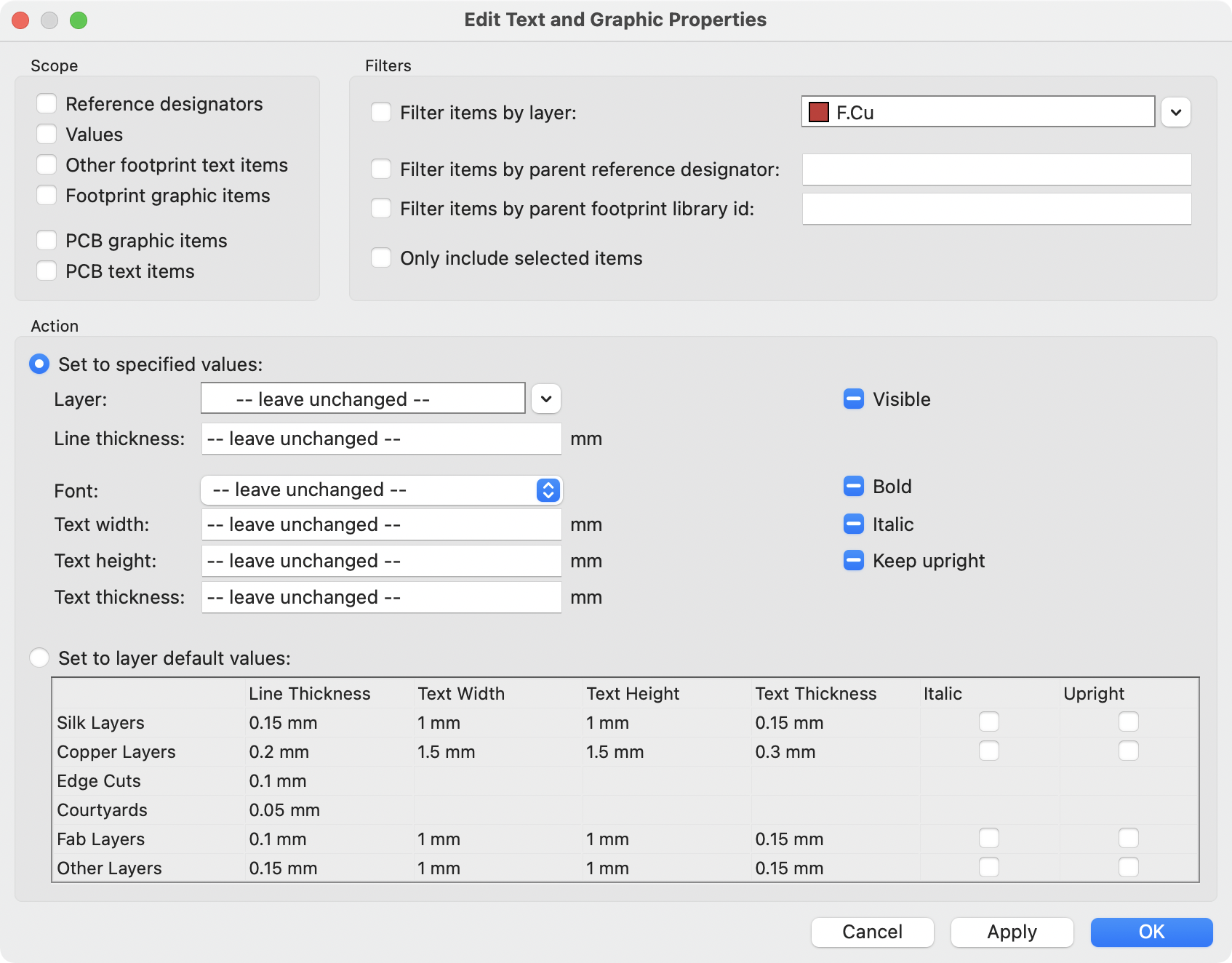
范围和筛选器
范围 设置限制了该工具只能编辑某些类型的对象。如果没有选择任何作用域,就不会有任何东西被编辑。
筛选器 限制该工具在选定的范围内编辑特定的对象。只有当对象符合所有启用的相关筛选器时才会被修改(有些筛选器不适用于某些类型的对象。例如,父封装筛选器不适用于图形项目,在改变图形属性时被忽略)。如果没有启用筛选器,所选范围内的所有对象都将被修改。对于带有文本框的筛选器,支持通配符。\* 匹配任何字符,? 匹配任何单个字符。
按层筛选项目 筛选到指定板层上的项目。
按名称筛选其他符号字段 筛选到指定的符号字段。
按父系位号筛选项目 筛选到封装中具有位号的字段。通过父系封装库 ID 筛选项目 筛选到封装中具有指定库标识符的字段。
只包括选定的项目 筛选到当前选择。
操作
被筛选对象的属性可以在对话框的底部设置为新值。通过选择 设置为指定值,可以将属性设置为任意值,或者通过选择*设置为图层默认值*,将属性重置为其图层的默认值。
下拉列表和文本框可以被设置为 --保持不变-- 以保留现有值。复选框可以被选中或不被选中,以启用或禁用一个变化,但也可以切换到第三个 "保持不变" 状态。
所有项目都可以设置其 层。
图形项目可以修改其 线的厚度。
可以修改的文本属性有 字体、文本宽度、文本高度、文本厚度(仅限 KiCad 字体)、强调(粗体 和 重体)和方向(保持直立)。封装文本也可以设置其 可见性。
标注
Dimensions are graphical objects used to show a measurement or other marking on a board design. They may be added on any drawing layer, but are normally added to one of the User layers. KiCad currently supports five different types of dimension: aligned, orthogonal, center, radial, and leader.
对齐 标注 (![]() ) 表示两点之间距离的测量。
测量轴是连接这两个点的线,标注图形与该轴保持平行。
) 表示两点之间距离的测量。
测量轴是连接这两个点的线,标注图形与该轴保持平行。
正交 标注 (![]() ) 也测量两点之间的距离,但测量轴是 X 轴或 Y 轴。
换句话说,这些标注表示两点之间距离的水平或垂直分量。
创建正交标注时,在选择要测量的两个点后,可以根据放置标注的位置选择要用作测量轴的轴。
) 也测量两点之间的距离,但测量轴是 X 轴或 Y 轴。
换句话说,这些标注表示两点之间距离的水平或垂直分量。
创建正交标注时,在选择要测量的两个点后,可以根据放置标注的位置选择要用作测量轴的轴。
中心 标注 (![]() ) 创建一个十字标记来指示一个点或圆或圆弧的圆心。
) 创建一个十字标记来指示一个点或圆或圆弧的圆心。
Radial dimensions (![]() ) show a measurement between
a center point and the outside of a circle or arc. The center point is indicated by a cross.
) show a measurement between
a center point and the outside of a circle or arc. The center point is indicated by a cross.
引线 标注 (![]() ) 创建一个箭头,将一条引线连接到文本字段。
此文本字段可以包含任何文本以及文本周围的可选圆形或矩形框。
这种类型的标注通常用来提醒人们注意设计的某些部分,以便在制造说明中参考。
) 创建一个箭头,将一条引线连接到文本字段。
此文本字段可以包含任何文本以及文本周围的可选圆形或矩形框。
这种类型的标注通常用来提醒人们注意设计的某些部分,以便在制造说明中参考。
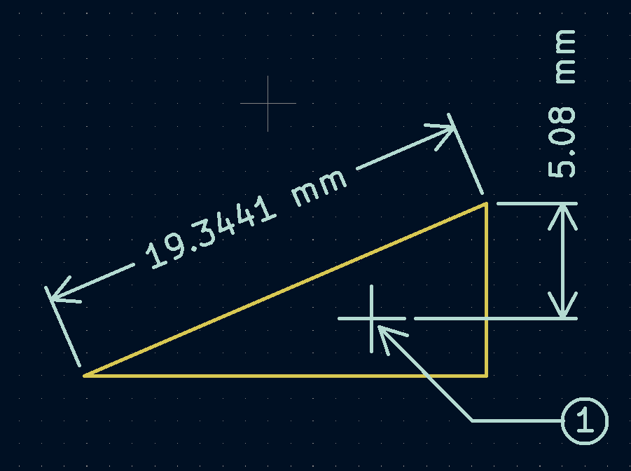
创建一个标注后,可以编辑其属性(快捷键 E)以改变显示数字的格式以及文本和图形线的风格。
| 您可以在电路板设置对话框的文本和图形默认值部分自定义新创建的标注对象的默认样式。 |
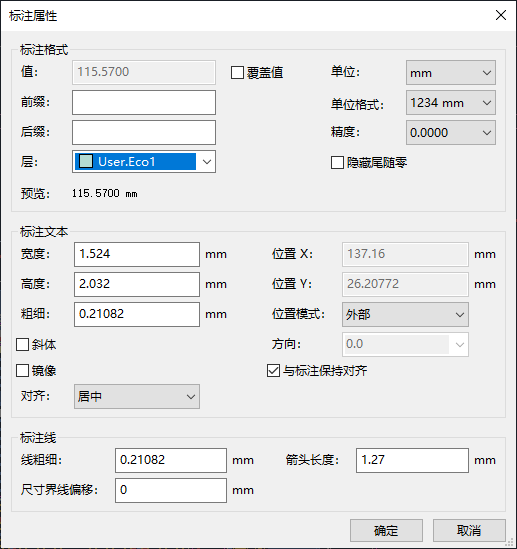
标注格式选项
覆盖值: 启用后,您可以直接在 值 字段中输入测量值,而不是实际测量值。
前缀: 此处输入的任何文字都将显示在测量值之前。
后缀: 此处输入的任何文字都将显示在测量值之后。
图层: 选择标注对象存在的层。
单位: 选择显示测量值的单位。 当更改电路板编辑器的显示单位时,自动 单位会导致标注单位发生变化。
单位格式: 从几种内置的单位显示风格中选择。
精度: 选择要显示多少位的精度。
标注文本选项
大多数标注文本选项与其他图形文本对象的选项相同(见上面的图形对象部分)。 也有一些特殊的选项适用于标注文本:
批注模式: 选择是手动定位批注文本,还是自动保持与批注测量线对齐。
与标注对齐: 开启后,标注文本的方向会自动调整,使文本与测量轴平行。
标注线选项
线条粗细: 设置构成标注形状的图形线的粗细。
标注界线偏移: 设置测量点到标注界线起点的距离。
箭头长度: 设置标注的形状的箭头段的长度。
引线选项
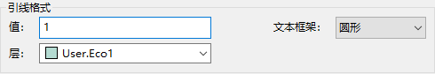
值: 输入要在引线行末尾显示的文本。
文本框架: 选择所需的文本周围的边界(圆形、矩形或无)。
布线
KiCad 具有交互式布线器的功能:
-
Allows manual or guided (semi-automatic) routing of single tracks and differential pairs
-
可通过以下方式修改现有设计:
-
拖动现有布线时重新布线现有布线
-
拖动封装时重新布线连接到封装焊盘的布线
-
-
允许通过插入蛇形线 + 来调整布线长度和差分对的偏移(相位) 为具有严格时序要求的设计调整布线形状
默认情况下,布线器在放置布线时尊重配置的设计规则:新布线的尺寸(宽度)将取自设计规则,在确定新布线和过孔的放置位置时,布线器将尊重设计规则中设置的铜间隙。 如果需要的话,可以通过使用高亮冲突布线器模式和打开布线器设置中的允许 DRC 违规选项来禁用这种行为(见下文)。
布线器有三种模式,可以随时选择。 布线器模式用于布线新布线,但也用于使用拖动(快捷键 D)命令拖动现有布线时。 这些模式是:
-
高亮冲突:在此模式下,大部分布线器功能被关闭,布线完全手动。 布线时,冲突 (间隙违规) 将以绿色高亮,如果存在冲突,则新布线的布线无法修复,除非打开了允许 DRC 冲突选项。 在此模式下,一次最多可以放置两个布线段 (例如,一个水平线段和一个对角线段)。
-
推挤:在此模式下,被布线的线段将绕过无法移动的障碍物 (例如,焊盘和锁定的布线/孔孔)和 推挤 障碍,这些障碍物可以移开。布线器在此模式下防止违反 DRC:如果无法布线到不违反 DRC 的光标位置,则不会创建新的布线。
-
绕走:在此模式下,布线器的行为与推挤模式相同,只是不会移动障碍物。
使用哪种模式是一个偏好问题。 对于大多数用户,我们建议使用推挤模式以获得最高效的布线体验,或者,如果您不希望布线器修改未被布线的线段,则建议使用绕走模式。请注意,推挤和绕走模式始终创建水平、垂直和 45 度 (H/V/45) 布线段。如果需要使用 H/V/45 以外的角度布线段,则必须使用高亮碰撞模式,并在交互布线器设置对话框中启用自由角度模式选项。
有五个主要的布线功能。单布线、差分对布线、调整单布线长度、调整差分对的长度和调整差分对的偏移 (相位)。 所有这些都存在于顶部工具栏上的路由菜单下拉菜单(单独)和绘图工具栏上的两个重载图标中,在右侧的绘图工具栏上。 上面介绍了重载图标的使用。 一个用于两个布线功能,一个用于三个调谐功能。 此外,布线菜单允许选择设置层对和交互式布线器设置。
To route tracks, click the Route Tracks ![]() icon (from the drawing toolbar or from the top toolbar under Route) or use the hotkey X. Click on a starting location to select which net to route and begin routing. The net being routed will automatically be highlighted and the allowable clearance for the net will be indicated with a gray outline around the tracks being routed. The clearance outline can be disabled by changing the Clearance Outlines setting in the Display Options section of the Preferences dialog.
icon (from the drawing toolbar or from the top toolbar under Route) or use the hotkey X. Click on a starting location to select which net to route and begin routing. The net being routed will automatically be highlighted and the allowable clearance for the net will be indicated with a gray outline around the tracks being routed. The clearance outline can be disabled by changing the Clearance Outlines setting in the Display Options section of the Preferences dialog.
| 间隙边框显示从布线网络到 PCB 上任何其他铜线的最大间隙。 可以使用自定义设计规则为不同对象指定网络的不同间隙。 布线器将考虑这些间隙,但仅直观地显示最大间距值。 |
当布线器处于活动状态时,将从布线起点到编辑器光标绘制新的线段。这些线段是未固定临时 (unfixed temporary) 对象,它们显示当您使用左击或 Enter 键来固定布线 (fix the route) 时将创建哪些线段。非固定布线段以比固定布线段更亮的颜色显示。当您使用 Esc 键或通过选择另一个工具退出布线器时,将只保存固定布线段。完成布线操作(快捷键 End) 将固定所有布线并退出布线器。
在布线时,可以使用撤消最后一个布线段命令 (快捷键 Backspace) 取消固定最近固定的布线。您可以重复使用此命令以后退已固定的布线。
In previous versions of KiCad, using the left mouse button or Enter to fix the routed segments would fix all segments up to but not including the segment ending at the mouse cursor location. In KiCad 6 and later, this behavior is optional, and by default, all segments including the one ending at the mouse cursor location will be fixed. The old behavior can be restored by disabling the "Fix all segments on click" option in the Interactive Router Settings dialog.
布线时,可以按住 Ctrl 键禁用网格捕捉,按住 Shift 键禁用对焊盘和过孔等对象的捕捉。
| 也可以通过更改首选项对话框的编辑选项部分中的磁吸点首选项来禁用对对象的捕捉。 我们建议您在一般情况下保持启用对象捕捉,这样就不会意外地在焊盘或过孔上略微偏离中心结束布线。 |
布线形态
在垂直(H) / 水平 (V) / 45 度模式下布线时,形态 是指一组两个线段如何连接单个 H/V/45 度线段无法到达的两个点。 在这种情况下,这些点将由一条水平或垂直线段和一条对角线 (45度) 线段连接。形态指的是这些线段的顺序:是水平/垂直线段还是对角线线段在前。

KiCad 的布线器试图根据一系列因素自动选择最佳形态。一般说来,布线器会尝试最大限度地减少路线中的拐角数量,并尽可能避免 "坏" 拐角 (如锐角)。当从焊盘布线或布线到焊盘时,KiCad 将选择将路线与焊盘最长边缘对齐的形态。
在某些情况下,KiCad 无法正确猜测您想要的形态。要在布线时切换布线的形态,请使用切换布线形态命令 (快捷键 /)。
在没有明显的“最佳”形态的情况下(例如,从过孔开始布线时),KiCad 将使用鼠标光标的移动来选择形态。如果希望布线从直线 (水平或垂直) 线段开始,请在水平或垂直方向上将鼠标从起始位置移开。如果您希望布线以对角线开始,请沿对角线方向移动。一旦光标与布线起始位置相距足够远,形态就会被锁定,并且除非光标回到起始位置,否则不会再更改。可以在交互式布线器设置对话框中禁用从鼠标光标移动检测形态,如下所述。
| 如果使用切换布线形态命令覆盖 KiCad 选择的形态,则在当前布线操作的其余部分中,将禁用从鼠标移动自动检测形体。 |
布线转角模式
当以 H/V/45 模式布线时,KiCad 的布线器可以放置尖角或圆角的布线。要在尖角和圆角之间切换,请使用布线拐角模式命令 (快捷键 Ctrl+/)。使用圆角布线时,每个布线步骤将放置直线段、单个圆弧或同时放置直线段和圆弧。布线形态决定首先放置圆弧还是直线段。
选择所需布线后,还可以在布线后使用圆角布线命令对布线拐角进行圆角处理。
| 尚不支持使用圆弧拖动布线。当拖动布线或在推挤模式下由布线器移动布线时,圆弧将转换回锐角。 |
布线宽度
被布线的线段的宽度是通过以下三种方式之一来确定的:如果布线的起点是现有线段的终点,并且顶部工具栏上的 ![]() 按钮被启用,宽度将被设置为现有布线的宽度。 否则,如果顶部工具栏中的布线宽度下拉菜单被设置为 "使用网络类宽度",则宽度将取自被布线的网络类(或任何为网络类指定不同宽度的自定义设计规则,例如在凹陷区域内)。 最后,如果布线宽度下拉菜单被设置为电路板设置对话框中配置的预定义布线尺寸之一,则将使用该宽度。
按钮被启用,宽度将被设置为现有布线的宽度。 否则,如果顶部工具栏中的布线宽度下拉菜单被设置为 "使用网络类宽度",则宽度将取自被布线的网络类(或任何为网络类指定不同宽度的自定义设计规则,例如在凹陷区域内)。 最后,如果布线宽度下拉菜单被设置为电路板设置对话框中配置的预定义布线尺寸之一,则将使用该宽度。
| 布线宽度永远不能低于在电路板设置对话框的约束部分中配置的最小布线宽度。如果添加的预定义宽度低于此最小约束,则将使用最小约束值。 |
KiCad 的布线器支持活动路线的单一布线宽度。 换句话说,要在线段中间改变宽度,你必须结束路线,然后从上一条线段的末端重新开始一条新的线段。 要改变活动线段的宽度,可使用快捷键 W 和 Shift+W,在电路板设置对话框中配置的布线宽度中逐步进行。
放置过孔
在布线线段时,切换层会在当前(未固定)线段的末端插入一个过孔。 一旦你放置了过孔,布线将继续在新层上进行。 有几种方法可以选择一个新层并插入过孔:
-
使用快捷键选择特定的图层,如 PgUp 选择
F.Cu或 PgDn 选择B.Cu。 -
通过使用 "下一层" 或 "上一层" 快捷键 (+ 和 -)。
-
通过使用 "放置过孔" 快捷键 (V),它将切换到活动层对中的下一层。
-
通过使用 "选择图层并通过通孔放置" 操作(快捷键 <),将打开一个对话框来选择目标层。
After using any of the above methods to add a via and change layer, but before clicking to fix the via and commit the current trace segment, you can cancel placing the via by pressing V. The via will be removed and routing will continue on the original layer.
You can place a via and end the current trace, without changing layers, by pressing V and then double-clicking or Shift-clicking to place the via.
过孔的尺寸将从激活的过孔尺寸设置中获取,可通过顶部工具栏的下拉列表或增加过孔尺寸 (') 和减小过孔尺寸 (\) 快捷键访问。与布线宽度非常相似,当通孔大小设置为"使用网络类尺寸" 时,将使用 "电路板设置" 的 "网络类" 部分中配置的过孔大小 (除非被自定义设计规则覆盖)。
如果在电路板设置对话框的约束条件部分启用了微孔或盲/埋孔,就可以在布线时放置这些过孔。 使用快捷键 Ctrl+V 来放置微孔,Alt+Shift+V 来放置盲/埋孔。 微孔只能被放置在连接一个外铜层和相邻层的位置。 盲孔/埋孔可以放置在任何一层上。
布线器放置的过孔被认为是已布线线段的一部分。 这意味着过孔网络可以自动更新(就像线段网络一样),例如,当从原理图中更新 PCB 时改变了线段的网络名。 在某些情况下,这可能是不需要的,例如在创建邮戳孔时。 对于特定的过孔,可以通过关闭过孔属性对话框中的 "自动更新过孔网络" 复选框来禁用过孔网络的自动更新。 使用 "添加独立过孔" 工具放置的过孔在创建时禁用这一设置。
Routing Convenience Functions
KiCad offers several functions to make certain routing operations more convenient.
If you need to route a number of traces from a set of pads, you can use the Route Selected tool to quickly route from each pad in sequence. Select the pads you want to use as starting points, then press Shift+X to route from each pad in sequence. The router will begin a trace from the first selected pad, which you can route as you would any other trace. When you complete the trace, the router will automatically begin a new trace from the next pad in the selection, in the same order that you selected the pads. Pads that already have traces attached are skipped. You can also skip routing the current trace and move on to the next pad by pressing Esc. You can also select footprints instead of pads; all unrouted pads in the selected footprints will be used as starting points.
If you want to route a number of traces to a set of pads, instead of from the pads, you can use the Route Selected From Other End tool (Shift+E). This tool works the same way as the Route Selected tool, except it uses each selected pad as an end point rather than a starting point. The starting point for each trace is the other end of the ratsnest line for each selected pad.
Routing from the other end is also possible while routing individual traces: press E while routing a trace to commit the current segment and begin routing from the other end of the in-progress trace’s ratsnest line.
Finally, you can quickly unroute traces connected to an object (footprint, pad, or trace) by selecting the object, right-clicking, and selecting Unroute Selected. Any traces connected to the selected object will be removed, starting at the selected object and continuing until another pad is encountered.
Automatically completing traces
KiCad’s router can automatically route individual traces, based on the connections defined in the schematic. This can be thought of as a limited form of auto-routing that considers a single trace at a time. The router will only use the current layer; it will not use vias or change layers.
While routing, press the F key to have the router attempt to automatically finish the current trace. The trace will be automatically routed from the end of the last fixed trace segment to the closest ratsnest anchor. If the router can’t automatically finish the trace, it will allow you to complete the trace manually. This action can also be performed by clicking Attempt Finish in the context menu while routing.
When the router is not the active tool, you can automatically route multiple traces by selecting footprints, pads, and traces to route from and pressing Shift+F. You do not need to select both ends of a desired connection; the router will route from the selected item to its nearest ratsnest anchor. If multiple items were selected, each item will be routed in sequence, in the order that they were selected. If a connection cannot be automatically completed, the tool will pause with the router active so that you can complete the trace manually. With the automatic completion paused for a manual connection, you can press Esc to skip routing the current trace. After manually completing the trace or skipping the connection, the tool will continue attempting to route the remaining connections.
差分对布线
KiCad 中的差分对被定义为具有共同的 基数名称 和正负后缀的网路。 KiCad 支持使用 ` 和 `-`,或者 `P` 和 `N` 作为后缀。 例如,`USB 和 USB- 构成一对差分,USB_P 和 USB_N 也是如此。 在第一个例子中,基本名称是 USB,第二个例子中是 USB_。 后缀样式不能混合:网路 USB+ 和 USB_N 不构成差分对。 请确保你在原理图中相应地命名你的差分对网络,以便在 PCB 编辑器中使用差分对布线器。
To route a differential pair, click the Route Differential Pairs ![]() icon (from the drawing toolbar or from the top toolbar under Route) or use the hotkey 6. Click on a pad, via, or the end of an existing differential pair track to start routing. You can start routing from either the positive or negative net of a differential pair.
icon (from the drawing toolbar or from the top toolbar under Route) or use the hotkey 6. Click on a pad, via, or the end of an existing differential pair track to start routing. You can start routing from either the positive or negative net of a differential pair.
| 目前不可能在现有差分对布线的中间开始对差分对进行布线。 |
差分对布线器将尝试用设计规则中的间隙布线这对布线(差分对间隙可以在电路板设置对话框的网络类部分中配置,也可以通过使用自定义设计规则来配置)。如果布线的起始或结束位置与配置的间隙不同,布线器将创建一个较短的 "扇出" 部分,以最大限度地缩短差分对未耦合的布线长度。
当交换层或使用放置过孔 (V) 操作时,差分对布线器将创建两个相邻的过孔。这些过孔将被放置在尽可能靠近彼此的位置,同时遵守铜和孔到孔间隙的设计规则。
修改布线
线段被布线后,可以通过移动或拖动来修改它们,或者删除并重新布线。 当选择一个线段时,快捷键 U 可以用来将选择范围扩大到所有连接的线段。 第一次按下 U 将选择与焊盘或过孔最近的连接点之间的线段。 第二次按 U 将再次扩大选择范围,包括所有层上与所选线段相连的所有线段。 用这种技术选择线段可以用来快速删除整个布线网络。
有两种不同的拖动命令可用于修改布线段。拖动 (45 度模式) 命令快捷键 D 用于通过布线器拖动布线。如果布线器模式设置为推挤,则使用此命令拖动将推挤附近的布线。如果布线器模式设置为绕走,则使用此命令拖动将绕过障碍物或停在障碍物处。拖动自由角度命令 快捷键 G 用于将布线段一分为二,并将新角点拖动到任何位置。拖动自由角度的行为类似于高亮碰撞布线器模式:不会避开或推挤障碍物,只会高亮。
| 目前还不能拖动包含圆弧的布线。在某些情况下,尝试拖动这些布线会导致圆弧被删除。可以通过选中特定圆弧并使用拖动命令 (D) 来调整其大小。使用此命令调整圆弧大小时,不执行 DRC 检查。 |
移动命令(快捷键 M)也可以在线段上使用。 该命令将拾取选定的线段,而忽略任何未被选中的附加线段或过孔。 使用移动命令移动线段时,不会进行 DRC 检查。
在移动封装的同时,可以对附着在封装上的线段进行重新布线。 要做到这一点,在选择了一个封装的情况下使用拖动命令(D)。 任何以封装的一个焊盘为终点的线段都将与封装一起被拖动。 这个功能有一些限制:它只在高亮冲突模式下运行,所以附着在封装上的线段不会绕过障碍物或将附近的线段推开。 此外,只有以封装的焊盘为终点的线段才会被拖动。 仅仅穿过焊盘或在原点以外的焊盘上结束的线段将不会被拖动。
可以使用编辑布线和过孔对话框修改布线的宽度和过孔的大小,而无需重新布线。有关详细信息,请参阅下面关于批量编辑工具的部分。
长度调整
The length tuning tools can be used to add serpentine tuning shapes to tracks after routing. To tune the length of a track, first pick the appropriate length tuning tool. The single track tuning tool (icon ![]() or hotkey 7) will add serpentine shapes to bring the length of a single track up to the target value. The differential pair tuning tool (icon
or hotkey 7) will add serpentine shapes to bring the length of a single track up to the target value. The differential pair tuning tool (icon ![]() or hotkey 8) will do the same for a differential pair. The differential pair skew tuning tool (icon
or hotkey 8) will do the same for a differential pair. The differential pair skew tuning tool (icon ![]() or hotkey 9) will add length to the shorter member of a differential pair in order to eliminate skew (phase difference) between the positive and negative sides of the pair. As with the Routing icons, the Tuning icons are found in both the Route menu dropdown from the top toolbar and the drawing toolbar on the right.
or hotkey 9) will add length to the shorter member of a differential pair in order to eliminate skew (phase difference) between the positive and negative sides of the pair. As with the Routing icons, the Tuning icons are found in both the Route menu dropdown from the top toolbar and the drawing toolbar on the right.
要选择长度调整工具的目标长度,请在激活长度调整工具后,从上下文菜单或使用快捷键 Ctrl+L 打开 "长度调整设置" 对话框:
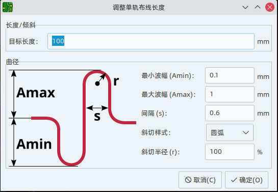
此对话框还可用于配置曲折形状的大小、形状和间距。
配置好目标长度后,在你希望开始放置蛇形形状的区域点击一个布线。 沿着线段移动鼠标光标,蛇形形状就会被添加。 光标旁边会出现一个状态窗口,显示布线的当前长度和目标长度。 再次点击,完成放置当前的蛇形布线。 如果需要,可以在同一条布线上放置多条蛇形布线。
| 长度调整工具仅支持调整两个焊盘之间的点对点网络的长度。尚不支持调整具有不同拓扑的网络长度。 |
交互式布线设置
交互式布线器设置可通过路径菜单访问,或通过右键单击工具栏中的布线按钮来访问。这些设置控制布线和拖动现有布线时的布线行为。
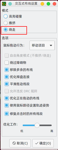
| 设置 | 说明 |
|---|---|
模式 |
设置用于创建新布线和拖动现有布线的路由器的操作模式。 有关详细信息,请参阅上面的内容。 |
自由角度模式 |
允许以任何角度布线,而不是仅以 45 度增量布线。 仅当布线模式设置为突出显示高亮冲突时, 此选项才可用。 |
绕过障碍物 |
在推挤模式下,允许布线尝试在实心障碍物 (如焊盘) 后面移动碰撞布线。 |
移除多余的布线 |
自动删除在当前布线中创建的回路, 仅保留回路中最近布线的部分。 |
优化焊盘连接 |
启用此设置时,交互式布线器尝试在退出焊盘和过孔时避免锐角 和其他不需要的布线。 |
平滑拖动线段 |
拖动布线时,会尝试将布线段组合在一起, 以最大限度地减少方向更改。 |
允许违反 DRC 规则 |
在高亮碰撞模式下,允许放置违反 DRC 规则的布线和过孔。 在其他模式下不起作用。 |
优化正在拖动的布线 |
启用后,拖动布线段将导致 KiCad 优化屏幕上可见的其余布线。 优化过程去除了不必要的拐角,避免了锐角,通常会尝试找到布线的最短路径。 禁用时,不会对正在拖动的紧邻部分之外的布线执行任何优化。 在拖动布线时尝试优化布线。 |
使用鼠标路径设置布线形态 |
尝试根据鼠标路径从布线起点位置拾取布线形态。 如果鼠标从开始位置开始主要沿对角线移动,则形态将设置为对角线起点; 如果鼠标主要水平或垂直移动,则形态将设置为垂直起点。 当鼠标离开布线起始位置很远时,形态估计就会被锁定, 并且可以通过移回起始位置来解锁。 |
点击时固定所有线段 |
启用时,在布线时单击将固定已布线的所有布线段的位置, 包括在鼠标光标结束的线段。新的线段将从鼠标光标位置开始。 禁用时,最后一个线段 (在鼠标光标处结束的线段) 将不会固定在适当位置, 可以通过进一步的鼠标移动进行调整。 |
向前和向后批注
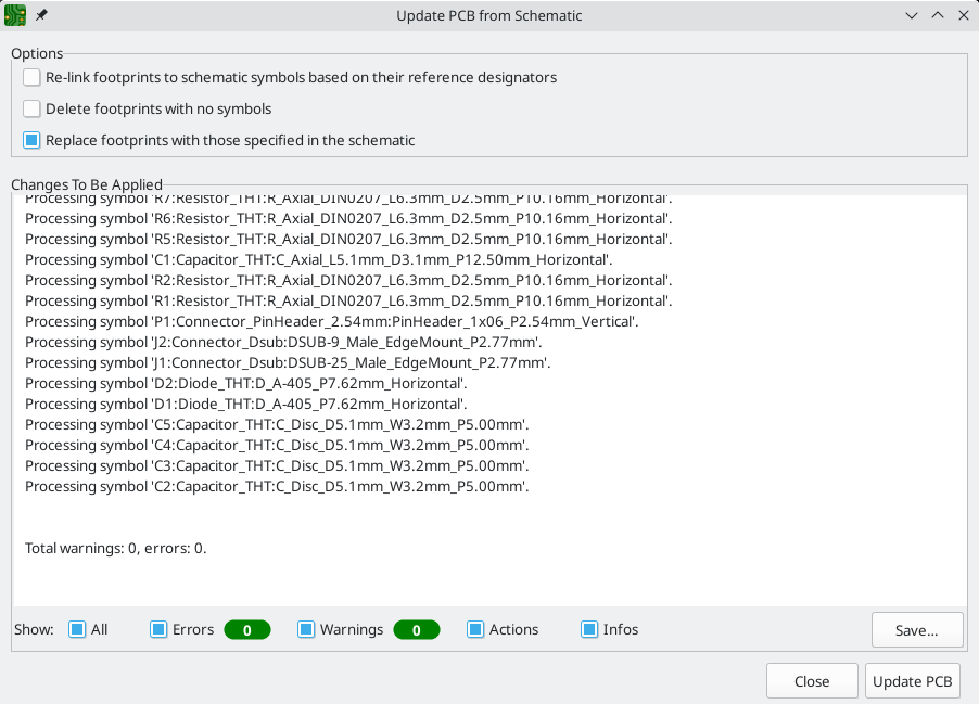
从原理图更新 PCB(正向批注)
使用 "从原理图更新 PCB" 工具将设计信息从原理图编辑器同步到电路板编辑器。在原理图编辑器和电路板编辑器中都可以用 工具 → 从原理图更新 PCB(F8)来访问该工具。你也可以使用电路板编辑器顶部工具栏上的 ![]() 图标。这个过程通常被称为正向批注。
图标。这个过程通常被称为正向批注。
| 从原理图更新 PCB 是将设计信息从原理图转移到 PCB 的首选方法。在旧版本的 KiCad 中,相应的过程是将网表从原理图编辑器中导出并导入到电路板编辑器中。现在已经没有必要使用网表文件了。 |
该工具将每个符号的封装添加到电路板上,并将更新的原理图信息传输到电路板上。特别是,电路板的网络连接被更新以符合原理图。
将对 PCB 进行的修改列在 待应用的修改 窗格中。在你点击 更新 PCB 按钮之前,PCB 不会被修改。
你可以使用窗口底部的复选框来显示或隐藏不同类型的信息。可以使用 保存… 按钮将更改的报告保存到文件中。
选项
该工具有几个选项来控制其行为。
| 选项 | 说明 |
|---|---|
根据位号将封装重新链接到原理图符号上 |
封装通常是通过符号添加到原理图中时创建的唯一标识符与原理图符号相连。符号的唯一标识符不能被改变。 如果选中,PCB 中的每个封装将被重新链接到与该封装具有相同位号的符号上。 如果不勾选,封装和符号将像往常一样通过唯一的标识符来链接,而不是通过位号。每个封装的位号将被更新以匹配其链接符号的位号。 这个选项一般不应该被选中。它对依赖改变原理图符号和封装之间的链接的特定工作流程很有用,例如重构原理图以方便布局,或者在设计的相同通道之间复制布局。 |
删除没有符号的封装 |
如果选中,PCB 中任何在原理图中没有相应符号的封装都将从 PCB 中删除。带有 "不在原理图中" 属性的封装将不受影响。 如果不勾选,没有相应符号的封装将不会被删除。 |
用原理图中指定的封装替换封装 |
如果选中,PCB 中的封装将被替换为相应原理图符号中指定的封装。 如果不勾选,即使原理图符号被更新为指定了不同的封装,PCB 中已有的封装也不会被改变。 |
从 PCB 上更新原理图(反向批注)。
KiCad 的典型工作流程是在原理图中进行修改,然后使用 "从原理图更新 PCB" 工具将修改内容同步到电路板上。然而,相反的过程也是可行的:可以在电路板上进行设计修改,然后在原理图或电路板编辑器中使用 工具 → 从 PCB 更新原理图 同步到原理图上。这个过程通常被称为反向批注。
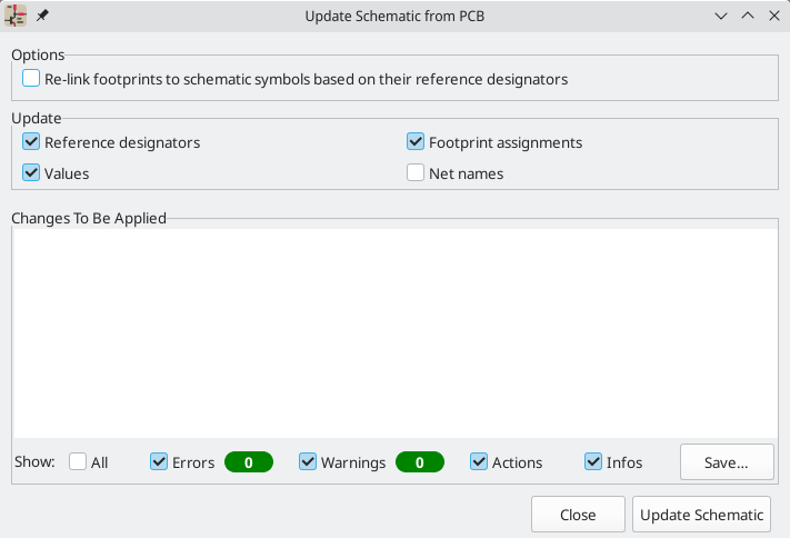
该工具将位号、值、封装分配和网络名称的变化从电路板同步到原理图。每种类型的变化都可以单独启用或禁用。
将对原理图进行的修改列在 待应用的修改 窗格中。在您点击 更新原理图 按钮之前,原理图不会被修改。
你可以使用窗口底部的复选框来显示或隐藏不同类型的信息。可以使用 保存… 按钮将更改的报告保存到文件中。
选项
该工具有几个选项来控制其行为。
选项 |
说明 |
根据位号将封装重新链接到原理图符号上 |
如果选中,PCB 中的每个封装将被重新链接到与该封装具有相同位号的符号上。这个选项与更新符号位号不兼容。 如果不勾选,封装和符号将像往常一样通过唯一的标识符连接,而不是通过位号。 |
位号 |
如果选中,符号位号将被更新,以匹配链接封装的位号。 如果不勾选,符号位号将不会被更新。 |
值 |
如果选中,符号值将被更新以匹配链接封装的值。 如果不勾选,符号值不会被更新。 |
封装分配 |
如果选中,符号的封装分配将被更新,这些符号的封装在电路板中被改变或替换。 如果不勾选,符号的封装分配将不会被更新。 |
网络名 |
如果选中,原理图将根据电路板上的任何网络名变化进行更新。如有必要,网络标签将被更新或添加到原理图中,以便与电路板相匹配。 如果不勾选,原理图中的网络名将不会被更新。 |
| 《全局重新批注,全局重新批注》功能可以与反向批注位号结合使用,根据设计中的位置重新批注所有元件。 |
用 CMP 文件进行反向批注
通过从 PCB 编辑器导出 CMP 文件(文件 → 导出 → 封装关联(.cmp)文件…)并在原理图编辑器中导入(文件 → 导入 → 封装分配…),也可以将选择的变化从 PCB 上同步到原理图。
| 这种方法只能同步对封装分配和封装字段的修改。建议使用 "从 PCB 更新原理图" 工具来代替。 |
位置重新批注
| This section of the KiCad documentation has not yet been written. We appreciate your patience as our small team of volunteer documentation writers work to update and expand the documentation. |
锁定
大多数对象可以通过其属性对话框、右键上下文菜单或使用 "切换锁定" 快捷键(L)来锁定。 被锁定的对象不能被选择,除非选择过滤器中的 "被锁定的项目" 复选框被启用。 试图移动锁定的项目将导致一个警告对话框:
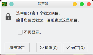
在这个对话框中选择 "覆盖锁定" 将允许移动锁定的项目。 选择 "确定" 将允许你在选择中移动任何未上锁的项目;留下锁定的项目。 选择 "不再显示" 将使你在剩下的会话中记住你的选择。
批量编辑工具
| This section of the KiCad documentation has not yet been written. We appreciate your patience as our small team of volunteer documentation writers work to update and expand the documentation. |
清理工具
| This section of the KiCad documentation has not yet been written. We appreciate your patience as our small team of volunteer documentation writers work to update and expand the documentation. |
正在导入图形
| This section of the KiCad documentation has not yet been written. We appreciate your patience as our small team of volunteer documentation writers work to update and expand the documentation. |
从 DXF 和 SVG 文件导入矢量图
| This section of the KiCad documentation has not yet been written. We appreciate your patience as our small team of volunteer documentation writers work to update and expand the documentation. |
正在导入位图图像
| This section of the KiCad documentation has not yet been written. We appreciate your patience as our small team of volunteer documentation writers work to update and expand the documentation. |
检查电路板
测量工具
测量工具允许你在 PCB 上的各点之间进行距离和角度测量。 要激活该工具,请点击右侧工具栏的 ![]() 图标,或使用快捷键 Ctrl+Shift+M。 一旦该工具被激活,点击一次以设置测量起点,然后再点击一次以完成测量。
图标,或使用快捷键 Ctrl+Shift+M。 一旦该工具被激活,点击一次以设置测量起点,然后再点击一次以完成测量。
| 测量工具用于不需要永久显示的快速测量。 您所做的任何测量都将仅在该工具处于活动状态时显示。 要创建将显示在打印输出和打印中的永久性尺寸标注,请使用尺寸标注工具。 |
设计规则检查
设计规则检查器用于验证 PCB 是否符合电路板设置对话框中建立的所有要求,以及所有焊盘是否按照网表或原理图连接。 KiCad 可以在布线线段时自动防止一些违反设计规则的行为,但许多其他的行为是无法自动防止的。 这意味着在为 PCB 创建制造文件之前,必须使用设计规则检查器。
要使用设计规则检查器,请点击顶部工具栏的 ![]() 图标,或从 检查 菜单中选择 设计规则检查器。
图标,或从 检查 菜单中选择 设计规则检查器。
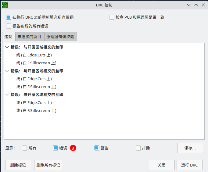
DRC 控制窗口的顶部部分包含一些控制设计规则检查器的选项:
重新填充所有敷铜后再执行 DRC: 启用后,每次运行设计规则检查器时都会重新填充敷铜。 如果未手动重新填充敷铜,禁用此选项可能会导致错误的 DRC 结果。
报告每个布线的所有错误: 启用后,将报告每个线段的所有间隙错误。 禁用时,将只报告第一个错误。 启用此选项将导致设计规则检查器运行速度变慢。
测试 PCB 和原理图之间的奇偶校验: 启用后,设计规则检查器除了测试 PCB 设计规则外,还将测试原理图和 PCB 之间的差异。 在独立模式下运行 PCB 编辑器时,该选项不起作用。
运行 DRC 后,任何违规行为都会显示在 DRC 控制窗口的中间部分。 违反规则、未连接的项目以及原理图和 PCB 之间的差异会显示在三个不同的标签中。 违规列表下面的控件可以用来显示或隐藏违规,这取决于其严重程度。 在运行 DRC 后,可以使用保存按钮创建一个纯文本格式的报告文件。
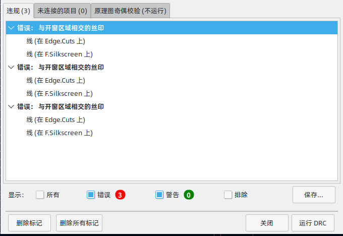
每个违规行为都涉及 PCB 上的一个或多个对象。 在违规列表中,涉及的对象列在违章下面。 点击列表中的违规行为将移动 PCB 编辑器的视图,使受影响的区域居中。 点击违规所涉及的对象之一将高亮显示该对象。
窗口底部的数字显示错误、警告和排除的数量。每种类型的违规行为都可以用各自的复选框从列表中过滤出来。点击 删除标记 将清除所有违规行为,直到再次运行 DRC。
可以在对话框中右键单击违规行为,以忽略它们或改变其严重程度:
-
排除此违规行为: 忽略此特定的违规行为,但不影响任何其他违规行为。
-
更改严重程度: 将一个违规类型从警告改为错误,或将错误改为警告。这影响到一个给定类型的所有违规行为。
-
忽略所有: 忽略所有给定类型的违规。这个测试现在将出现在 忽略的测试 标签,而不是 违反 标签。
在设计规则检查器运行期间,排除的和忽略的违规行为会被记住。
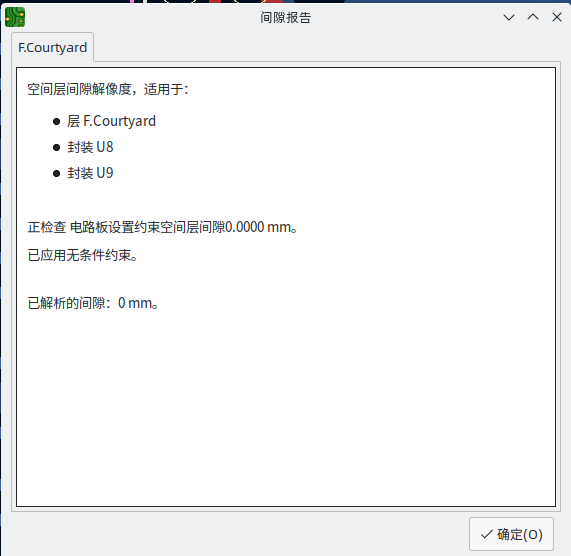
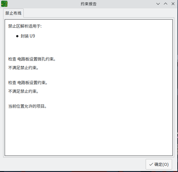
间隙和约束解析
间隙和约束解决工具允许你检查哪些间隙和设计约束规则适用于选定的项目。 当设计具有复杂设计规则的 PCB 时,这些工具可以提供帮助,因为在这种情况下并不总是清楚哪些规则适用于某个对象。
要检查两个对象之间适用的间隙规则,选择这两个对象并从 检查 菜单中选择 间隙分辨率。 间隙报告对话框将显示每个铜层上的对象之间所需的间隙,以及产生该间隙的设计规则。
要检查适用于一个对象的设计约束,选择它并从 检查 菜单中选择 约束解析。 约束报告对话框将显示适用于该对象的任何约束。
查找工具
查找工具在 PCB 中搜索文本,包括位号、封装区域和图形文本。当该工具找到一个匹配的文本时,画布会被放大,并将其置于匹配文本的中心位置,同时文本被高亮显示。使用顶部工具栏中的(![]() )按钮启动该工具。
)按钮启动该工具。
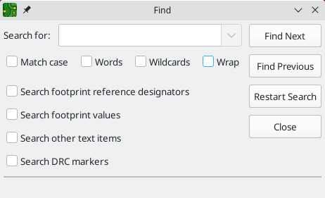
查找工具有几个选项:
匹配大小写: 选择搜索是否对大小写敏感。
关键词: 当选择时,搜索将只与 PCB 中的完整单词相匹配。当未选择时,如果搜索词是 PCB 中一个较大的词的一部分,搜索将匹配。
通配符: 当选择时,通配符可以在搜索词中使用。? 匹配任何单个字符,* 匹配任何数量的字符。请注意,当选择这个选项时,不会返回部分匹配结果:搜索 abc* 将匹配字符串 abcd,但搜索 abc 则不会。
缠绕: 选择后,搜索结果将在达到最后一次点击后返回到第一次点击。
搜索封装位号: 选择搜索是否应适用于封装位号。
搜索封装值: 选择搜索是否应适用于封装值字段。
搜索其他文本项目: 选择搜索是否应适用于其他文本项目,包括图形文本和除值和位号之外的封装字段。
搜索 DRC 标记: 选择搜索是否应适用于板上显示的 DRC 标记的违规描述。
搜索面板
| This section of the KiCad documentation has not yet been written. We appreciate your patience as our small team of volunteer documentation writers work to update and expand the documentation. |
3D 查看器
3D 查看器显示了电路板和电路板上的元件的 3D 视图。你可以从不同的角度查看电路板,显示或隐藏不同类型的元件,从 PCB 编辑器到 3D 查看器的交叉探测,以及生成电路板的光线跟踪渲染图。
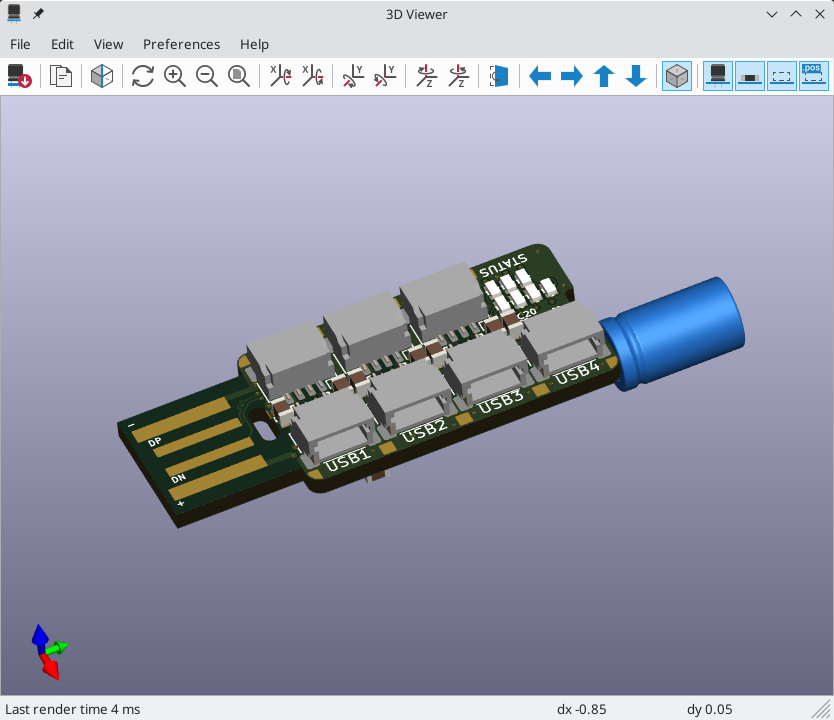
| The 3D model for a component will only appear if the 3D model file exists and has been assigned to the footprint. |
| KiCad 标准库中的许多封装还没有为它们创建模型文件。然而,这些封装可能包含一个指向尚不存在的 3D 模型的路径,以期待将来创建 3D 模型。 |
浏览 3D 视图
Dragging with the left mouse button will orbit the 3D view. By default this is the centroid of the board, but the pivot point can be reset to a new point on the board by moving the cursor over the desired point and pressing Space. Scrolling the mouse wheel will zoom the view in or out. Scrolling while holding Ctrl pans the view left and right, and scrolling while holding Shift pans up and down. Dragging with the middle mouse button also pans the view.
不同大小的 3D 网格可以用 偏好设置 → 3D 网格 菜单来设置。每个元件的围框可以通过 偏好设置 → 显示模型围框 来启用。
当 PCB 编辑器和 3D 查看器同时打开时,在 PCB 编辑器中选择一个封装也会在 3D 查看器中突出显示该元件。高亮显示的颜色可以在 偏好设置 → 偏好设置… → 3D 查看器 → 实时渲染器 → 选择颜色 中调整。
用 3D 查看器生成图像
当前的 3D 视图可以用 文件 → 将当前视图导出为 PNG… 或 将当前视图导出为 JPG…,根据所需的图像格式,将其保存为一个图像。也可以用 ![]() 按钮,或 编辑 → 复制 3D 图像 将当前视图复制到剪贴板上。
按钮,或 编辑 → 复制 3D 图像 将当前视图复制到剪贴板上。
3D 查看器有一个光线跟踪渲染模式,它使用比默认渲染模式更精确的物理渲染模型来显示电路板。 光线追踪比默认渲染模式慢,但当需要最吸引人的视觉效果时,可以使用它。使用 ![]() 按钮,或者使用 偏好设置→光线追踪 来启用光线追踪模式。在光线追踪模式下,3D 网格和选择高光不会显示。
按钮,或者使用 偏好设置→光线追踪 来启用光线追踪模式。在光线追踪模式下,3D 网格和选择高光不会显示。
颜色和其他渲染选项,包括光线跟踪和非光线跟踪模式,都可以在 偏好设置 → 偏好设置… → 3D查看器 中调整。
3D 查看器控制
许多查看选项是通过顶部的工具栏控制的。
|
Reload the 3D model |
|
Copy 3D image to clipboard |
|
Render current view using raytracing |
|
Redraw |
|
Zoom in |
|
Zoom out |
|
Fit drawing in display area |
|
Rotate X clockwise |
|
Rotate X counterclockwise |
|
Rotate Y clockwise |
|
Rotate Y counterclockwise |
|
Rotate Z clockwise |
|
Rotate Z counterclockwise |
|
Flip board view |
|
Pan board left |
|
Pan board right |
|
Pan board up |
|
Pan board down |
|
Enable/disable orthographic projection |
|
Show/hide 3D models for through-hole components |
|
Show/hide 3D models for surface mount components |
|
Show/hide 3D models for components of type 'other' |
|
Show/hide 3D models for components not in position file |
网络检查
网络检查器允许你查看电路板中所有网络的统计数据。 要打开检查器,请点击外观面板中的网络部分顶部的 ![]() 图标,或者从检查菜单中选择网络检查器。
图标,或者从检查菜单中选择网络检查器。
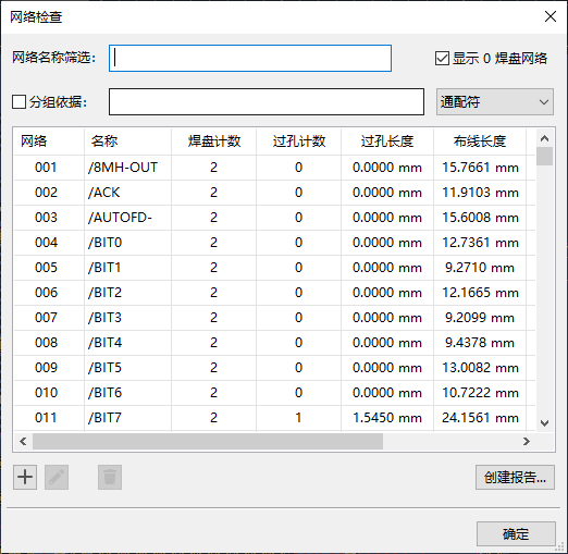
点击网络列表中的一个网络会在电路板上高亮显示该网络。 单击列标题允许您按该列对网络列表进行排序。
分组依据字段允许您将不同的网络组合在一起,并查看组合的网络的总长度。 例如,如果您有两个名为 DATA0 和 DATA0_EXT 的网络,则使用值为 DATA0* 的分组依据将创建一个包含这两个网络的组。 通过将分组依据模式从通配符更改为 RegEx (正则表达式),可以创建更复杂的分组。 分组依据模式的子字符串 (Substr) 变体将为以不同方式匹配该模式的每组网络创建组。
例如,如果您有 U1D+,U1D-,U2D+ 和 U2D-,分组模式 U*D 将在通配符模式下匹配所有四个网络,创建一个单一的组 U*D。 在通配符子串模式下,它将匹配所有四个网络,但创建两个不同的组:U1D 和 U2D。
焊盘计数 和 过孔计数 显示一个网的焊盘(表面贴装和通孔)和过孔的数量。 过孔长度 显示每个过孔的总高度(不考虑过孔连接到哪个铜层)。 换句话说,过孔长度等于过孔数乘以电路板的堆积高度。 布线长度 显示一个网络中所有布线段的总长度,不考虑拓扑结构。 芯片长度 显示了网络中所有焊盘设置的焊盘长度值的总和。
| 网络检查器中显示的长度不同于长度调整工具中显示的长度, 因为网络检查器显示连接到网络的所有布线的总和, 而长度调整工具显示最近的两个焊盘或分支过孔之间的距离。 有关长度调整工具的更多信息,请参见布线部分。 |
生成输出
KiCad 可以生成和导出多种不同格式的文件,对制造 PCB 和与外部软件的接口很有用。 该功能可在文件菜单的几个不同部分中找到。 制造输出部分包含准备制造 PCB 所需的最常见操作。 输出部分包含生成可由外部软件读取的文件的工具。 绘图功能允许你以各种格式导出 PCB 的 2D 线图。 打印功能允许你将 PCB 的视图发送到 2D 打印机上。
制造输出和绘制
KiCad 使用 Gerber 文件作为其 PCB 制造的主要绘图格式。 要创建 Gerber 文件,请从文件菜单中打开绘图对话框,或从文件菜单的制造输出部分选择 Gerbers。 绘图对话框将打开,允许你配置和生成 Gerber 文件。
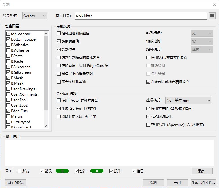
绘制选项
包含层: 检查列表中是否启用了您的电路板上使用的每一层。 将不打印禁用的图层。
输出目录: 指定打印文件的保存位置。 如果这是相对路径,则它是相对于工程目录创建的。
打印边框和标题栏: 如果启用,将在每个图层上打印图纸边框和标题栏。 打印 Gerber 文件时,通常应禁用此功能。
绘制封装值: 如果启用,每个封装的值字段将绘制在其所在的任何层上 (除非特定封装的字段可见性被禁用)。
绘制位号: 如果启用,每个封装的位号字段将绘制在其所在的任何层上 (除非特定封装的字段可见性被禁用)。
强制绘制不可见值/位号: 如果启用,将绘制所有封装值和位号,即使其中一些字段禁用了字段可见性。
在所有图层上绘制 Edge.Cuts: 如果启用,Edge.Cuts(电路板边框) 图层将添加到所有其他层。 请向您的制造商咨询,了解此设置对于其制造过程的正确值是多少。
制造层上的草图焊盘: 如果启用,制造 (F.Fab,B.Fab) 层上的封装焊盘将绘制为未填充的边框,而不是填充的形状。
请勿覆盖过孔: 如果启用,过孔将不会覆盖在阻焊层 (F.Mask、B.Mask) 上。 如果禁用,过孔将由阻焊层 (绿油) 覆盖。
| KiCad 不支持覆盖或开窗特定过孔。 覆盖只能是全局控制的(一块板上的所有过孔)。 |
钻孔标记: 对于 Gerber 以外的绘图格式,可以在所有钻孔的位置绘制标记。 钻孔标记可以按成品孔的实际尺寸 (直径) 上创建,也可以在更小的尺寸上创建。
缩放: 对于支持非 1:1 缩放的打印格式,可以设置打印比例。 自动缩放设置将缩放绘图以适合指定的页面大小。
绘制模式: 对于某些绘制格式,填充的形状可能只被绘制成边框(草图模式)。
使用钻孔/放置文件原点: 启用后,绘制文件的坐标原点将是电路板编辑器中设置的钻孔/放置文件原点。 禁用时,坐标原点将是绝对原点 (图框的左上角)。
镜像绘制: 当设置该选项时,对于某些绘制格式,可能会水平镜像输出。
负片绘制: 对于某些绘制格式,可能会将输出设置为负片模式。 在此模式下,将为电路板边框内的空白区域绘制图形,并在 PCB 中存在对象的位置留下空白区域。
绘制前检查敷铜填充: 启用后,将在生成输出之前检查敷铜填充 (如果过期则重新填充)。 如果禁用此选项,绘制输出可能不正确!
Gerber 选项
使用 Protel 文件扩展名: 启用后,绘制的 Gerber 文件将使用基于 Protel (.GBL、.GTL 等) 的文件扩展名命名。
当禁用时,文件将有 .gbr 的扩展名。
生成 Gerber 作业文件: 开启后,Gerber 作业文件 (.gbrjob) 将与任何 Gerber 文件一起生成。
Gerber 作业文件是 Gerber 格式的扩展,包括有关 PCB 压层、材料和表面处理的信息。
有关 Gerber 工作文件的更多信息,请访问链接:Ucamco 网站。
坐标格式: 配置坐标在绘制的 Gerber 文件中的存储方式。 请咨询您的制造商,了解他们对此选项的推荐设置。
使用扩展 X2 格式: 启用后,绘制的 Gerber 文件将使用 X2 格式,其中包括有关网表和其他扩展属性的信息。 此格式可能与某些制造商使用的旧版 CAM 软件不兼容。
包含网表属性: 启用后,绘制的 Gerber 文件将包含可用于在 CAM 软件中检查设计的网表信息。 禁用 X2 格式模式时,此信息将作为注释包含在 Gerber 文件中。
禁用光圈宏: 启用后,所有形状将作为基元绘制,而不是使用光圈宏。 此设置仅在制造商要求时用于与旧的或有错误的 CAM 软件兼容。
Postscript 选项
缩放系数: 控制棋盘文件中的坐标将如何被缩放到 PostScript 文件中的坐标。 使用不同的 X 和 Y 比例因子的值将导致输出的拉伸/扭曲。 这些系数可以用来纠正 PostScript 输出设备中的缩放比例,以实现精确的输出比例。
布线宽度校正: 在绘制 PostScript 文件时,从布线、过孔和焊盘的尺寸中添加(或减去,如果是负的)一个全局系数。 这个系数可用于纠正 PostScript 输出设备中的错误,以实现精确的比例输出。
强制 A4 输出: 启用后,生成的 PostScript 文件将为 A4 大小,即使 KiCad 电路板文件大小不同。
SVG 选项
单位: 控制 SVG 文件中使用的单位。 由于 SVG 格式没有指定的单位系统, 因此您必须使用与导入到其他软件时要使用的单位设置相同的单位设置进行导出。
精度: 控制将使用多少个有效数字来存储坐标。
DXF 选项
使用图形项目的边框绘制图形项目: DXF 文件中的图形形状没有宽度。 此选项控制如何将 KiCad 电路板中具有宽度 (厚度) 的图形图形绘制到 DXF 文件。 启用此选项后,将绘制形状的外边框。 禁用此选项时,将打印形状的中心线 (并且形状的厚度在生成的 DXF 文件中不可见)。
使用 KiCad 字体绘制文本: 启用后,KiCad 设计中的文本将使用 KiCad 字体绘制为图形形状。 禁用时,文本将作为 DXF 文本对象绘制,它将使用不同的字体,并且不会以与 KiCad 电路板编辑器中显示的完全相同的位置和大小显示。
导出单位: 控制将在 DXF 文件中使用的单位。 由于 DXF 格式没有指定的单位系统,因此您必须使用与导入到其他软件时要使用的单位设置相同的单位设置进行导出。
HPGL 选项
默认笔尺寸: 控制用于创建图形的绘图仪笔尺寸。
钻孔文件
KiCad 可以生成大多数 PCB 制造工艺所需的 Excellon 或 Gerber X2 格式的数控钻孔文件。 KiCad 还可以生成钻孔图:一个显示钻孔位置的电路板图形图。 从 "制造输出" 菜单中选择 "生成钻孔文件" 选项来打开该对话框:
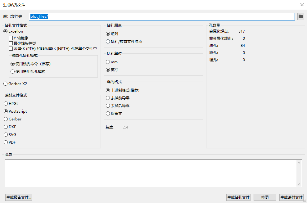
输出文件夹: 选择要保存生成的钻孔和映射文件的文件夹。 如果输入相对路径,则它将相对于工程目录。
钻孔文件格式: 选择是生成 Excellon 钻孔文件 (大多数 PCB 制造商都需要)还是 Gerber X2 文件。
镜像 Y 轴: 对于卓越文件,选择是否镜像 Y 轴坐标。 当由第三方制造 PCB 时,通常不应使用该选项,并且是为了方便自己制造 PCB 的用户而提供的。
最小钻头: 对于 Excellon 文件,选择是否输出最小钻头,而不是完整的文件钻头。 除非制造商要求,否则不应启用此选项。
PTH (电镀孔) 和 NPTH (非电镀孔) 为单文件: 默认情况下,会在两个不同的 Excellon 文件中生成电镀孔和非电镀孔。 启用此选项后,这两个文件将合并为单个文件。 除非制造商要求,否则不应启用此选项。
椭圆孔钻孔模式: 控制椭圆孔在 Excellon 钻孔文件中的表示方式。 默认设置 使用布线命令 对于大多数制造商都是正确的。 如果制造商要求,请仅选择 使用备用钻孔模式 设置。
映射文件格式: 选择绘制钻孔映射的输出格式。
钻孔原点: 选择钻孔文件的坐标原点。 绝对 将使用左上角的页面原点。 钻孔/放置文件原点 将使用电路板设计中指定的原点。
钻孔单位: 选择钻孔坐标和尺寸的单位。
零的格式 控制 Excellon 钻孔文件中数字的格式。 请根据制造商的建议在此处选择一个选项。
元件放置文件
元件放置文件是一种文本文件,它列出了电路板上的每个元件(封装)以及其中心位置和方向。 这些文件通常用于对取放机进行编程,如果你订购的是完全组装的 PCB,你的制造商可能需要这些文件。
| 如果为生成的封装启用了“从放置文件中排除”选项,该封装将不会出现在生成的放置文件中。 这可用于排除不代表要组装的物理元件的某些封装。 |
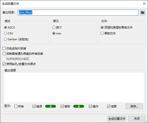
格式: 选择生成纯文本 (ASCII)、逗号分隔文本 (CSV) 或 Gerber 放置文件格式。
单位: 在放置文件中选择元件位置的单位。
文件: 选择是为电路板正面和背面的封装生成单独的文件,还是生成一个合并两面的文件。
只包括 SMD 封装: 启用后,将只包括具有 SMD 制造属性的封装。 请与您的制造商联系,以确定是否应将非 SMD 封装纳入或排除在位置文件之外。
使用通孔焊盘排除所有封装: 启用时,如果封装包含任何通孔焊盘,即使其制造类型设置为 SMD,也将从放置文件中排除封装。
包括电路板边缘层: 对于 Gerber 放置文件,控制电路板边框是否包含在封装放置数据中。
使用钻孔/放置文件原点: 启用后,元件位置将相对于电路板设计中设置的钻孔/放置文件原点。 禁用时,位置将相对于页面原点 (左上角)。
额外的制造产出
KiCad 还可以从电路板设计生成封装报告文件、IPC-D-356 网表文件和物料清单 (BOM)。 这些输出格式没有可配置的选项。
打印
KiCad 可以使用文件菜单中的打印操作将电路板视图打印到标准打印机上。
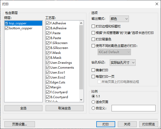
Include layers: Select the layers to include in the printout. Unselected layers will be invisible. Right-click the list for layer selection commands.
输出模式: 选择以黑白或全彩方式打印。
Print drawing sheet: When enabled, the page border and title block will be printed.
根据外观管理器的对象选项卡打印: 启用后,任何隐藏在外观面板的对象选项卡中的对象都将隐藏在打印输出中。 禁用时,如果在包含的图层区域中选择了这些对象所在的图层,则将打印这些对象。
打印背景色: 全彩色打印时,该选项控制是否打印视图背景色。
使用不同的颜色主题进行打印: 当以全色打印时,此选项允许使用不同的颜色主题进行打印。 禁用时,电路板编辑器使用的颜色主题将用于打印。
钻孔标记: 控制是以实际大小显示钻孔,还是以较小的尺寸显示钻孔,还是将其隐藏在打印输出中。
打印镜像: 启用后,打印输出将被水平镜像。
每层打印一页: 启用后,在包含图层区域中选择的每一图层都将打印到单独一页。 如果启用此选项,在所有页面上打印电路板边缘 选项控制是否将 Edge.Cuts 层添加到每个打印页面。
比例: 控制打印输出相对于页面设置中配置的页面大小的比例。
正在导出文件
KiCad 可以将电路板设计导出为各种第三方格式,以便与外部软件一起使用。 这些功能可以在文件菜单的导出部分找到。
Specctra .DSN: 创建适合导入到某些第三方自动布线软件中的文件。 此导出器没有可配置的选项。
| TODO:文档 GenCAD 导出器 |
| TODO: 文档 VRML 导出器 |
IDF 导出器
IDF 导出器导出一个 IDFv3 兼容的板(.emn)和库(.emp)文件,用于向机械 CAD 软件包传递机械尺寸。导出器导出板子的边框和切口,所有的焊盘和安装孔,包括开槽孔,以及元件的边框;这是与机械设计师互动所需的最基本的机械数据集。IDFv3 规范中描述的所有其他实体目前都没有导出。
| 你必须将 IDF 元件模型附加到你的设计的封装中,然后它们才会被包含在导出的模型中。关于将模型附加到封装的更多信息,请参阅《创建和编辑封装,封装文档》。一些针对 IDF 的指导包括在《使用 idf 元件边框的工作,高级主题文档》中。 |
| 关于创建 IDF 元件模型的更多信息,包括 KiCad 中包含的 IDF 实用工具的描述,请参阅《使用 idf 元件边框的工作,高级主题文档》。 |
一旦为所有需要的元件指定了模型,就可以导出电路板的模型。在 PCB 编辑器中,选择文件 → 导出 → IDFv3…。
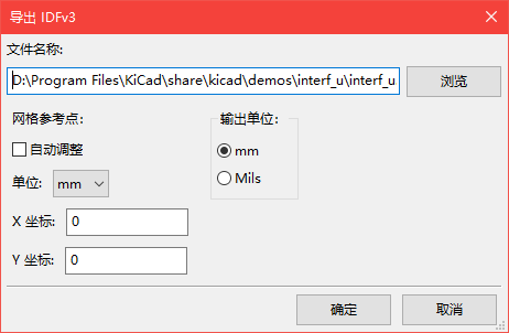
网格参考点: 选择导出的模型参考点的位置。如果选择了 自动调整 选项,KiCad 将把参考点设置为 PCB 的中心点。否则,参考点将相对于显示原点设置。
输出单位: 选择输出模型的单位是毫米还是密耳。
输出结果可以直接在机械 CAD 应用程序中查看,或使用《idf2vrml,idf2vrml 工具》转换为 VRML。
| TODO: 文档 STEP 导出器 |
| TODO: 文档 SVG 导出器 |
| TODO: 文档 CMP 文件导出器 |
Hyperlynx: 创建适合导入 Mentor Graphics(Siemens) HyperLynx 模拟和分析软件的文件。
封装和封装库
管理封装库
KiCad 的封装库管理系统允许直接使用几种类型的封装库:
-
KiCad
.pret封装库(以 .pret 为扩展名的文件夹,包含 .kicad_mod 文件)。 -
KiCad 遗留封装库(.mod 文件)
-
GEDA 库(包含 .fp 文件的文件夹)
-
Eagle 封装库
KiCad 只支持写到 KiCad 的本地 .pretty 格式的封装库(以及其中的 .kicad_mod 封装文件)。所有其他封装库格式都是只读的。
|
KiCad 使用一个封装库表,将任何支持的库类型的封装库映射到库的昵称。KiCad 使用一个全局封装库表,以及一个针对每个工程的表。要编辑任何一个封装库表,请使用 偏好设置→ 管理封装库…。
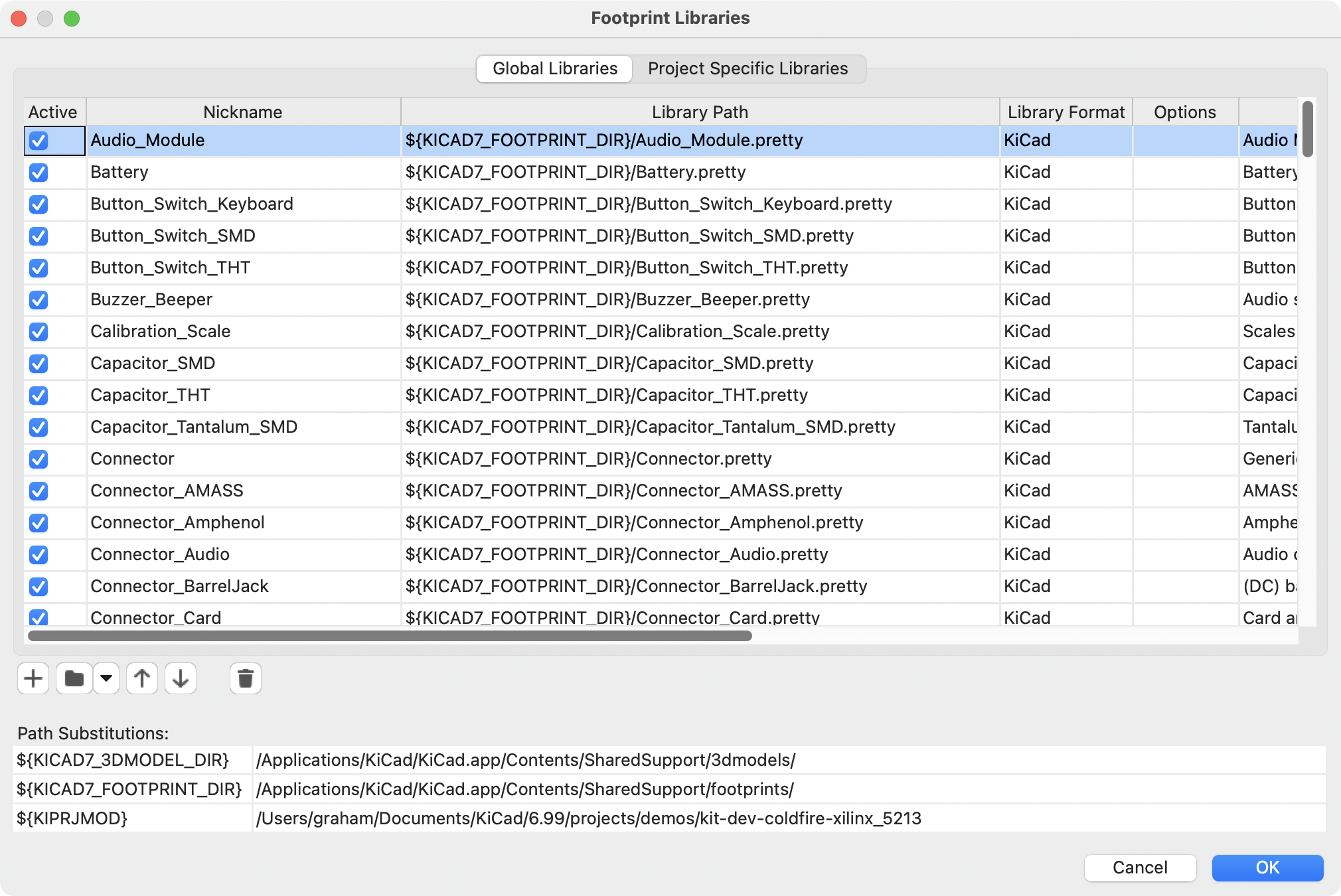
全局封装库表包含了无论当前加载的工程是什么,都可以使用的库列表。该表保存在 KiCad 配置文件夹中的 fp-lib-table 文件中。该文件夹的位置 取决于正在使用的操作系统。
工程专用的封装库表包含了专门为当前加载的工程提供的库的列表。如果有任何工程专用的封装库,该表将保存在工程文件夹中的 fp-lib-table 文件中。
初始配置
当 PCB 编辑器(或任何其他使用封装的 KiCad 工具)第一次运行时,如果没有找到全局封装表文件 fp-lib-table,KiCad 将引导用户设置一个新的封装库表。这个过程被描述为《初始配置》。
管理表的条目
封装库只有在被添加到全局或工程专用的封装库表中时才能被使用。
通过点击 ![]() 按钮并选择一个库或点击
按钮并选择一个库或点击 ![]() 按钮并输入库文件的路径来添加一个库。选定的库将被添加到当前打开的库表中(全局或工程专用)。可以通过选择所需的库条目并点击
按钮并输入库文件的路径来添加一个库。选定的库将被添加到当前打开的库表中(全局或工程专用)。可以通过选择所需的库条目并点击 ![]() 按钮来删除库。
按钮来删除库。
这个 ![]() 和
和![]() 按钮在库表中上下移动所选库。这并不影响在 "封装库浏览器"、"封装编辑器 "或 "添加封装工具 "中显示库的顺序。
按钮在库表中上下移动所选库。这并不影响在 "封装库浏览器"、"封装编辑器 "或 "添加封装工具 "中显示库的顺序。
库可以通过取消勾选第一列中的 活动 复选框而变得不活动。不活动的库仍然在库表中,但不会出现在任何库的浏览器中,也不会从磁盘加载,这可以减少加载时间。
通过点击范围内的第一个库,然后 Shift -点击范围内的最后一个库,就可以选择一个库的范围。
每个库必须有一个独特的昵称:在同一个表中不允许有重复的库昵称。然而,昵称可以在全局和工程库表中重复。工程表中的库比全局表中的同名库更有优先权。
库的昵称不一定要与库的文件名或路径有关。冒号字符 (:) 不能用于库昵称或封装名称,因为它被用作昵称和封装之间的分隔符。
每个库条目必须有一个有效的路径。路径可以定义为绝对的、相对的,或者通过《环境变量替换,环境变量替换》来定义。
必须选择适当的库格式,以便正确读取库。KiCad 支持读取 KiCad (.pretty), KiCad 遗留 (.mod), Eagle (.lbr), 和 GEDA (带有 .fp 文件的文件夹)封装库。
有一个可选的描述字段,用于添加库条目的描述。选项字段目前不使用,所以添加选项在加载库时不会有任何影响。
环境变量替代
封装库表支持环境变量替换,这允许你定义环境变量,其中包含存储库的自定义路径。环境变量替换是通过在封装库路径中使用 ${ENV_VAR_NAME} 的语法来支持的。
By default, KiCad defines several environment variables which are described in the project manager documentation. Environment variables can be configured in the Preferences → Configure Paths… dialog.
在封装库表中使用环境变量,可以在不破坏封装库表的情况下重新定位库,只要在库的位置改变时更新环境变量即可。
${KIPRJMOD} is a special environment variable that always expands to the absolute path of the current project directory. ${KIPRJMOD} allows libraries to be stored in the project folder without having to use an absolute path in the project library table. This makes it possible to relocate projects without breaking their project library tables.
使用 GitHub 插件
| KiCad 在 6.0 版本中取消了对 GitHub 库插件的支持。 |
创建和编辑封装
| This section of the KiCad documentation has not yet been written. We appreciate your patience as our small team of volunteer documentation writers work to update and expand the documentation. |
自定义焊盘形状
封装属性
| 在这里提到网节点 |
封装向导
有关创建新的封装向导的更多信息,请参阅高级主题一章的脚本部分。
高级主题
配置和自定义
KiCad PCB 编辑器有多种偏好设置,可通过偏好设置对话框进行配置。像 KiCad 的所有部分一样,PCB 编辑器的偏好设置存储在用户配置目录中,并且在 KiCad 的次要版本之间是独立的,以允许多个版本的偏好设置并排运行。
偏好设置对话框的第一部分(通用、鼠标和触摸板以及快捷键)是所有 KiCad 程序共享的。这些部分在 KiCad 手册中的 "常规偏好设置" 部分有详细描述。
显示选项
渲染引擎: 控制是否使用硬件加速图形或软件加速图形。
网格样式: 控制如何绘制路线网格。
网格厚度: 控制网格线或网格点的粗细。
最小网格间距: 控制两条网格线之间的最小距离 (以像素为单位)。无论当前的栅格设置如何,都不会绘制违反此最小间距的栅格线。
捕捉到网格: 控制何时将绘制和编辑操作捕捉到活动网格上的坐标。 “始终”将启用对齐,即使网格处于隐藏状态; “当网格显示时”将仅在网格可见时启用对齐。
| 按住 Ctrl 可以暂时禁用网格捕捉。 |
光标形状: 控制编辑光标是绘制为小十字准线还是全屏十字准线 (覆盖整个绘图画布的一组线)。 编辑光标显示下一个绘图或编辑操作将发生的位置,如果启用了捕捉,则会捕捉到栅格位置。
始终显示十字准线: 控制是始终显示编辑光标, 还是仅在编辑或绘图工具处于活动状态时才显示编辑光标。
网络名称: 控制是否在铜对象上绘制网络名称标签。 这些标签仅作为编辑指南,不会出现在制造输出中。
显示焊盘编号:控制是否在封装焊盘上绘制焊盘编号标签。
显示焊盘 <无网络> 指示器: 控制是否用特殊标记指示没有 网络的焊盘。
布线间隙: 控制是否显示布线和过孔周围的间隙边框。 间隙边框显示为对象周围的细长形状,表示与其他对象之间的最小间隙, 如约束和设计规则所定义。
显示焊盘间隙: 控制是否显示焊盘周围的间隙边框。
交叉探测项目的中心视图: 当原理图和 PCB 编辑器同时运行时,控制在原理图中点击一个元件或引脚是否会将 PCB 编辑器的视图集中在相应的封装或焊盘上。
缩放以适合交叉探测项: 控制是否缩放视图以显示交叉探测 封装或焊盘。
高亮交叉探测网络: 控制当高亮工具在两个工具中激活时,原理图中高亮的网络是否会在 PCB 编辑器中高亮。
编辑选项
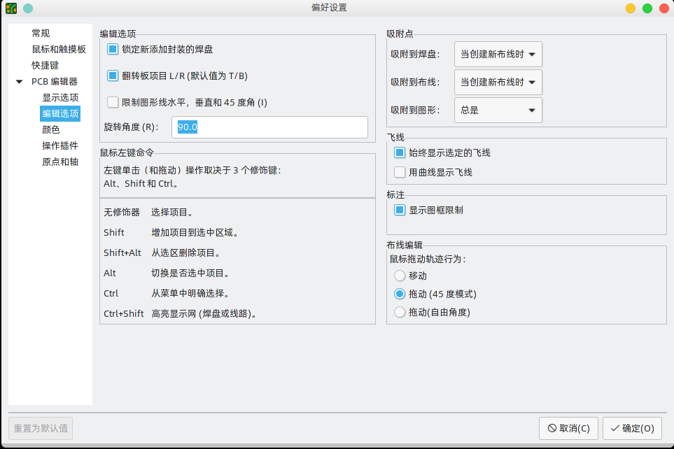
翻转电路板项目 L/R: 控制在顶层和底层之间移动电路板项目时翻转的方向。 选中时,项目从左向右翻转(围绕垂直轴); 取消选中时,项目从上向下翻转(围绕水平轴)。
旋转命令的步长: 控制每次使用旋转命令时选定对象将旋转多远。
允许自由焊盘: 控制封装焊盘是否可以解锁并与封装分开编辑或移动。
吸附点: 本节控制对象捕捉,也叫吸附点。 启用对象捕捉后,对象捕捉优先于网格捕捉。 物体捕捉只对活动层上的物体起作用。按住 Shift 可以暂时关闭对象捕捉功能。
捕捉焊盘: 控制编辑光标何时捕捉焊盘原点。
捕捉到布线: 控制编辑光标何时捕捉到布线端点。
对齐图形: 控制编辑光标何时对齐图形形状点。
始终显示选定的飞线:启用后,即使全局飞线被隐藏, 选定封装外形的飞线也将始终显示。
用曲线显示飞线:控制飞线是直线绘制还是曲线绘制。
鼠标拖动布线行为: 控制使用鼠标拖动布线段时将发生的操作:"移动" 将独立于任何其他布线段移动布线。 "拖动(45 度模式)" 将调用推挤式布线器拖动布线,遵守设计规则并保持其他布线段的连接。 "拖动(自由角度)" 将移动布线段最近的角点,高亮显示与其他对象的碰撞,但不会将其移开。
将图形线条限制为 H、V 和45度: 控制使用图形绘制工具绘制的布线是否可以采用任何角度。 请注意,这仅影响绘制新的布线:可以编辑布线以采用任何角度。
显示页面限制: 控制页面边界是否绘制为矩形。
覆铜属性后重新填充覆铜对话框: 控制编辑任何覆铜的属性后是否自动重新填充覆铜。 可以在复杂的设计或速度较慢的计算机上禁用此功能,以提高响应速度。
颜色
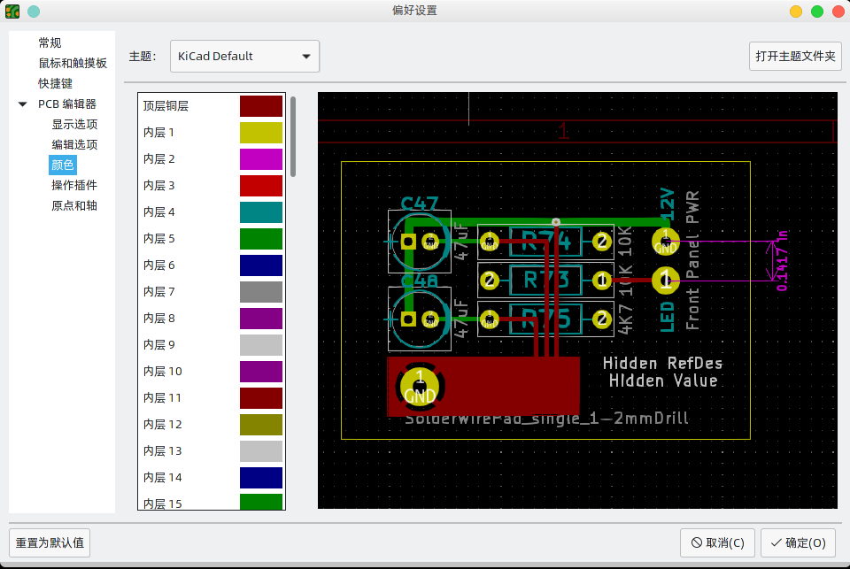
KiCad 支持在不同的颜色主题之间切换,以符合你的喜好。Kicad 7.0 内置了两种颜色主题。"KiCad 默认" 是一个新的主题,旨在为大多数情况下提供良好的对比度和平衡,是新安装的默认主题。"KiCad 经典版" 是 KiCad 5.1 和早期版本的默认主题。这两个内置主题都不能被修改,但你可以创建新的主题来定制 KiCad 的外观,也可以安装其他用户制作的主题。
颜色主题存储在位于 KiCad 配置目录的 Colors 子目录中的 JSON 文件中。“打开主题文件夹”按钮将在您的系统文件管理器中打开此位置,使您可以轻松地管理已安装的主题。要安装新主题,请将其放在此文件夹中,然后重新启动 KiCad。如果文件是有效的颜色主题文件,则新主题将从颜色主题下拉列表中提供。
要创建一个新的颜色主题,从颜色主题的下拉列表中选择新主题…。 为你的主题输入一个名称,然后开始编辑颜色。 新主题中的颜色将从你创建新主题之前选择的任何主题中复制。
要更改颜色,请双击或中键单击列表中的色样。“重置为默认值”按钮会将该颜色重置为“KiCad 默认”颜色主题中的相应条目。
颜色主题会自动保存;当您关闭偏好设置对话框时,所有更改都会立即反映出来。对话框右侧的窗口显示所选主题外观的预览。
操作插件
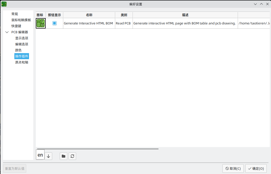
KiCad PCB 编辑器支持用 Python 编写的插件,可以对正在编辑的电路板进行操作。 这些插件可以使用内置的插件和内容管理器来安装(详见 KiCad 章节),或者将插件文件放在用户的插件目录中。 详见下面的脚本部分。
每个被检测到的插件都会在这个偏好设置上显示一排。 插件可以在 PCB 编辑器的顶部工具栏上显示一个按钮。 如果一个插件的 "显示按钮" 控制没有被选中,它仍然可以从 "工具" > "外部插件" 菜单中访问。
列表底部的箭头控制允许改变插件在工具栏和菜单中的显示顺序。 文件夹按钮将启动一个文件资源管理器到插件文件夹,以使安装新的插件更容易。 刷新按钮将扫描插件文件夹中的任何新的或删除的插件,并更新列表。
原点和轴
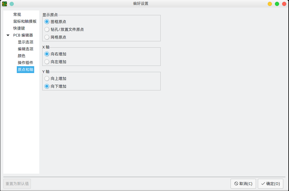
显示原点: 决定在编辑画布中坐标显示使用哪个坐标原点。 页面原点固定在页面的角落。 用户可以移动钻取/放置文件原点和栅格原点。
X 轴: 控制 X 坐标向右还是向左增加。
Y 轴: 控制 Y 坐标是向上还是向下增加。
Text variables
KiCad supports text variables, which allow you to substitute the variable name with a defined text string. This substitution happens anywhere the variable name is used inside the variable replacement syntax of ${VARIABLENAME}.
You can define your own text variables in the schematic or board setup dialogs, but there are also a number of built-in system text variables. System text variables may be available in some contexts and not others.
The following variables can be used in PCB text, footprint text, and footprint fields. There are also a number of variables that can be used in the Schematic Editor.
| Variable name | Description |
|---|---|
|
Contents of drawing sheet’s |
|
Today’s date, in ISO format. |
|
Contents of drawing sheet’s |
|
Contents of drawing sheet’s |
|
Contents of drawing sheet’s |
|
Contents of drawing sheet’s |
|
Layer of the object. In footprint fields, this is the layer of the parent footprint. |
|
Contents of project text variable
|
|
Contents of footprint field Both built-in footprint fields and user-defined fields from the
corresponding symbol are available. Built-in footprint fields use all
uppercase letters: for example, to access a footprint’s value, use
Built-in footprint fields are |
|
Contents of field Both built-in footprint fields and user-defined fields from the
corresponding symbol are available. Built-in footprint fields use all
uppercase letters: for example, to access the value of Built-in footprint fields are |
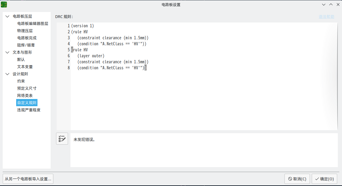
自定义设计规则
KiCad 的自定义设计规则系统允许创建比电路板设置对话框的约束页面中的通用规则更具体的设计规则。 自定义设计规则有很多应用,但一般来说,它们被用来对电路板的一部分应用某些规则,如特定的网络或网络类、特定的区域或特定的封装。
自定义设计规则存储在一个扩展名为 kicad_dra 的单独文件中。当您开始向项目添加自定义规则时,会自动创建此文件。如果您在项目中使用自定义规则,请在备份或提交到版本控制系统时,确保将 kicad_dra 文件与 kicad_pcb 和 kicad_pro 文件一起保存。
kicad_dra 文件由 KiCad 自动管理,不应使用外部文本编辑器进行编辑。
始终使用电路板设置对话框的自定义规则页面编辑自定义设计规则。
|
自定义规则编辑器
自定义规则编辑器位于电路板设置对话框中,它提供了一个用于输入自定义规则的文本编辑器,一个语法检查器将测试你的自定义规则并指出任何错误,还有一个语法帮助对话框,其中包含了对自定义规则语言的快速参考和一些规则示例。
最好在编辑自定义规则后使用 检查规则语法 按钮,以确保没有语法错误。自定义规则中的任何错误都将阻止设计规则检查器运行。
自定义规则语法
自定义设计规则语言基于 s 表达式,允许您创建使用内置约束无法实现的设计约束。每条设计规则通常包含一个定义匹配哪些对象的 条件,以及一个定义要应用于匹配对象的规则的 约束。
该语言使用圆括号 (( 和 )) 来定义相关标记和值的子句。括号必须始终匹配:对于每个 ( 必须有匹配的 )。在子句中,标记和值之间用空格分隔。按照惯例,使用单个空格,但是可以在标记之间使用任意数量的空格字符。在文本字符串有效的地方,没有任何空格的字符串可以用 " 或 ' 引起来,也可以不加引号。包含空格的字符串必须始终用引号引起来。在需要嵌套引号的地方,可以使用 " 作为外引号字符,使用 ' 作为内引号字符 (反之亦然),从而实现单层嵌套。换行符不是必需的,但为清楚起见,通常在示例中使用。
在下面的语法描述中,< 尖括号 > 中的项表示必须存在的标记,[ 方括号 ] 中的项表示可选或仅有时需要的标记。
The Custom Rules file must start with a version header defining the version of the rules language. As of KiCad 7.0, the version is 1. The syntax of the version header is (version <number>). So in KiCad 7.0 the header should read:
(version 1)
在版本标题之后,您可以输入任意数量的规则。规则以相反的顺序计算,这意味着首先检查文件中的最后一个规则。一旦找到正在测试的给定集合对象的匹配规则,将不再检查其他规则。实际上,这意味着更具体的规则应该在文件的后面,以便在评估更一般的规则之前对其进行评估。
例如,如果您创建一条规则来限制网络 HV 中的布线与任何其他网络中的布线之间的最小间距,以及第二条规则来限制特定规则区域内所有对象的最小间距,请确保第一条规则在自定义规则文件中的出现时间比第二条规则晚,否则,如果 HV 网络中的布线落在规则区域内,可能会有错误的间距。
Each rule must have a name and one or more constraint clause. The name can be any string and is used to refer to the rule in DRC reports. The constraint defines the behavior of the rule. Rules may also have a condition clause that determines which objects should have the rule applied, an optional layer clause, which specifies which board layers the rule applies to, and an optional severity clause which specifies the severity of the resulting DRC violation.
(rule <name>
    [(severity <severity>)]
    [(layer <layer_name>)]
    [(condition <expression>)]
    (constraint <constraint_type> [constraint_arguments]))
The custom rules file may also include comments to describe rules. Comments are denoted by any line that begins with the # character (not including whitespace). You can press Ctrl+/ to comment or uncomment lines automatically.
# Clearance for 400V nets to anything else
(rule HV
    (condition "A.NetClass == 'HV'")
    (constraint clearance (min 1.5mm)))
图层子句
层 (layer) 子句确定规则将对哪些层起作用。虽然对象层可以在下面介绍的 约束 (constraint) 子句中进行测试,但是使用 层 (layer) 子句效率更高。
层 (layer) 子句的值可以是任何线路板层名,也可以是与顶底铜层 ( F.Cu 和 B.Cu ) 匹配的快捷方式 外 (outer),以及与任何内部铜层匹配的快捷键 内 (inner)。
如果省略 层 (layer) 子句,则该规则将适用于所有层。
下面是一些示例:
# Do not allow footprints on back layer (no condition clause means this rule always applies)
(rule "Top side footprints only"
    (layer B.Cu)
    (constraint disallow footprint))

# This rule does the same thing, but is less efficient
(rule "Top side footprints only"
    (condition "A.Layer == 'B.Cu'")
    (constraint disallow footprint))

# Larger clearance on outer layers (inner layer clearance set by board minimum clearance)
(rule "clearance_outer"
    (layer outer)
    (constraint clearance (min 0.25mm)))
Severity Clause
The severity clause sets the DRC violation severity whenever the rule is violated.
Possible values are error, warning, ignore, and exclusion. Ignored rules are not observed by the interactive router and violations are not shown in the DRC dialog. However, ignored rules are evaluated for matching and therefore can still override earlier rules. Errors, warnings, and excluded rules are all observed by the interactive router, and violations are displayed in the DRC dialog when the appropriate filters are selected.
Setting a rule’s severity to ignore does not disable the rule; only the effects of the rule are disabled. The rule is still evaluated and can still override previous rules.
|
条件子句
规则 条件 是一个包含在文本字符串中的表达式(因此通常用引号包围,以便允许留出空白,使之更清晰)。 该表达式是针对设计规则检查器正在测试的每一对对象进行评估的。 例如,当检查铜对象之间的间隙时,每个网络上的每个铜对象(布线段、焊盘、通孔等)都要与其他网络上的其他铜对象进行检查。 如果存在一个自定义规则,其表达式与两个给定的铜对象相匹配,并且约束条件定义了铜的间隙,那么这个自定义规则可以用来确定这两个对象之间所需的间隙。
被测对象在表达式语言中称为 A 和 B。这两个对象的顺序并不重要,因为设计规则检查器将测试这两种可能的顺序。例如,您可以编写一条规则,假设 A 为布线,B 为过孔。 有一些表达式函数可以同时测试这两个对象;这些表达式函数使用 AB 作为对象名。
条件中的表达式必须解析为布尔值 ( true 或 false )。如果表达式解析为 true,则规则应用于给定的对象。
每个被测对象都有可以比较的 属性,以及可以执行特定测试的 函数。属性和函数的使用语法分别为 <object>.<property> 和 <object>.<function>([arguments])。译者注: <对象>.<属性> 和 <对象>.<函数>([参数])。
当您在文本编辑器 ( A.、B. 或 AB. ) 中键入 <对象 (object)>. 时,会出现一个自动完成列表。将打开包含所有可使用的对象属性的。
|
The object properties and functions are compared using boolean operators to result in a boolean expression. The following operators are supported:
|
等于 |
|
不等于 |
|
大于、大于或等于 |
|
小于、小于或等于 |
|
和 |
|
或 |
For example, A.NetClass == 'HV' will apply to any objects that are part of the "HV" netclass and A.NetClass != B.NetClass will apply to any objects that are in different netclasses. Parentheses can be used to clarify the order of operations in complex expressions but they are not required. All the boolean operators have the same precedence and are evaluated in order from left to right.
有些属性表示物理测量,比如尺寸、角度、长度、位置等等。 在这些属性上,单位后缀 可以在自定义规则语言中使用,以指定使用什么单位。 如果没有使用单位后缀,属性的内部表示将被使用(距离为纳米,大多数角度为度)。 支持以下后缀:
|
毫米 |
|
千分之一英寸 (mils) |
|
英寸 |
|
度 |
|
弧度 |
| 自定义设计规则中使用的单位独立于 PCB 编辑器中的显示单位。 |
Numeric conditions can use simple math expressions, for example (condition "A.Hole_Size_X == 1.0mm + 0.1mm").
约束
规则的 约束 子句定义了规则在条件匹配的对象上的行为。每个约束子句都有一个 约束类型 和一个或多个设置约束行为的参数。单个规则可以有多个约束子句,以便为符合相同规则条件的对象设置多个约束 (如 间隙 (clearance)、布线宽度 (trace_width) )。
许多约束条件的参数指定了一个物理测量或数量。 这些约束条件支持最小值、最优值和最大值说明(缩写为 "min/opt/max")。 最小 和 最大 值用于设计规则检查:如果实际值小于约束条件中的最小值或大于最大值,将产生一个 DRC 错误。 最优 值仅用于某些约束,并通知 KiCad 默认使用的 "最优" 值。 例如,最优的 diff_pair_gap 是由布线器在放置新的差分对时使用的。 如果后来修改了差分对,使得差分对之间的间隙与最佳值不同,只要间隙在最小值和最大值之间(如果这些值被指定),就不会产生错误。 在所有接受最小/最大/最优值的情况下,可以指定任何或全部的最小值、最优值和最大值。
最小/最优/最大值被指定为 (min<value>), (opt<value>), 和 (max<value>)。例如,布线宽度约束可以写成 (constraint track_width (min 0.5mm) (opt 0.5mm) (max 1.0mm)),如果只约束最小宽度,可以简单写成 `(constraint track_width (min 0.5mm))。
Numeric constraint values can use simple math expressions, for example (constraint clearance (min 0.5mm + 0.1mm)).
| Constraint type | Argument type | Description |
|---|---|---|
|
min/opt/max |
Checks the width of annular rings on vias. |
|
boolean expression |
Checks that the boolean expression is true. If the expression is false, a DRC error will be created. The expression can use any of the properties listed in the Object Properties section. |
|
min |
Checks the clearance between copper objects of different nets. KiCad’s design rule system does not permit constraining clearance between objects on the same net at this time. To allow copper objects to overlap (collide), create a |
|
min |
Checks the width of connections between pads and zones. An error will be generated for each pad
connection that is narrower than the |
|
min |
Checks the clearance between footprint courtyards and generates an error if any two courtyards
are closer than the |
|
min/opt/max |
Checks the gap between coupled tracks in a differential pair. Coupled tracks are segments that are parallel to each other. Differential pair gap is not tested on uncoupled portions of a differential pair (for example, the fanout from a component). |
|
max |
Checks the distance that a differential pair track is routed uncoupled from the other polarity track in the pair (for example, where the pair fans out from a component, or becomes uncoupled to pass around another object such as a via). |
|
|
Specify one or more object types to disallow, separated by spaces. For example,
|
|
min/opt/max |
Checks the clearance between objects and graphical items on the |
|
min |
Checks the clearance between a drilled hole in a pad or via and copper objects on a different net. The clearance is measured from the diameter of the hole, not its center. |
|
min/max |
Checks the size (diameter) of a drilled hole in a pad or via. For oval holes, the smaller
(minor) diameter will be tested against the |
|
min |
Checks the clearance between mechanically-drilled holes in pads and vias. The clearance is measured between the diameters of the holes, not between their centers. HDI vias (microvias, blind vias, and buried vias) are not tested by this constraint. |
|
min/max |
Checks the total routed length for the nets that match the rule condition and generates an
error for each net that is below the |
|
|
Checks the total number of connections (spokes) to a pad. An error will be raised for each pad that has fewer than the specified number of spokes. |
|
min |
Checks the clearance between two objects on a given layer (including non-copper layers). While this can perform more general-purpose checks than |
|
min |
Checks the clearance between a drilled hole in a pad or via and another object, regardless of net. The clearance is measured from the diameter of the hole, not its center. This can also be thought of as the "drilling tolerance" as it only includes round holes
(see |
|
min/opt/max |
Checks the clearance between objects on silkscreen layers and other objects. |
|
max |
Checks the total skew for the nets that match the rule condition, that is, the difference
between the length of each net and the average of all the lengths of each net that is matched
by the rule. If the absolute value of the difference between that average and the length of
any one net is above the constraint |
|
min/max |
Checks the height of text, including text boxes. An error will be generated for each text item
that has a height below the |
|
min/max |
Checks the thickness of text, including text boxes. An error will be generated for each text
item that has a thickness below the |
|
min |
Specifies the width of the gap between a pad and a zone with a thermal-relief connection. |
|
opt |
Specifies the width of the spokes connecting a pad to a zone with a thermal-relief connection. |
|
min/opt/max |
Checks the width of track and arc segments. An error will be generated for each segment that
has a width below the |
|
max |
Counts the number of vias on every net matched by the rule condition. If that number exceeds
the constraint |
|
min/max |
Checks the diameter of vias. An error will be generated for each via that has a diameter below
the |
|
|
Specifies the connection to be made between a zone and a pad. |
对象属性和函数参考
可以在自定义规则表达式中测试以下属性:
常见属性
这些属性适用于所有 PCB 对象。
| Property | Data type | Description |
|---|---|---|
|
string |
The board layer on which the object exists. For objects that exist on more than one layer,
this property will return the first layer (for example, |
|
boolean |
True if the object is locked. |
|
string |
Returns the unique identifier of the parent object of this object. |
|
dimension |
The position of the object’s origin in the X-axis. Note that the origin of an object is not always the same as the center of the object’s bounding box. For example, the origin of a footprint is the location of the (0, 0) coordinate of that footprint in the footprint editor, but the footprint may have been designed such that this location is not in the center of the courtyard shape. |
|
dimension |
The position of the object’s origin in the Y-axis. Note that KiCad always uses Y-coordinates that increase from the top to bottom of the screen internally, even if you have configured your settings to show the Y-coordinates increasing from bottom to top. |
|
string |
One of "Footprint", "Pad", "Graphic Shape", "Board Text", "Footprint Text", "Zone", "Track", "Via", "Zone", or "Group". |
连接的对象属性
这些属性适用于可以分配网的铜对象(焊盘、过孔、覆铜、布线)。
| Property | Data type | Description |
|---|---|---|
|
integer |
The net code of the copper object. Note that net codes should not be relied upon to remain
constant: if you need to refer to a specific net in a rule, use |
|
string |
The name of the netclass for the copper object. |
|
string |
The name of the net for the copper object. |
封装属性
这些属性适用于封装。
| Property | Data type | Description |
|---|---|---|
|
dimension |
The copper clearance override set for the footprint. |
|
string |
The "Description" from the library footprint. |
|
boolean |
True if the footprint’s "Do not populate" attribute is set. |
|
boolean |
True if the footprint’s "Exclude from position files" attribute is set. |
|
boolean |
True if the footprint’s "Exclude from bill of materials" attribute is set. |
|
boolean |
True if the footprint’s "Exempt from courtyard requirement" attribute is set. |
|
string |
The "Keywords" from the library footprint. |
|
string |
The link to the library footprint in |
|
boolean |
True if the footprint’s "Not in schematic" attribute is set. |
|
double |
The orientation (rotation) of the footprint in degrees. |
|
string |
The reference designator of the footprint. |
|
dimension |
The solder paste margin override set for the footprint. |
|
dimension |
The solder paste margin ratio override set for the footprint. |
|
dimension |
The thermal relief gap set for the footprint. |
|
dimension |
The thermal relief connection width set for the footprint. |
|
string |
The contents of the "Value" field of the footprint. |
|
string |
One of "Inherited", "None", "Thermal reliefs" or "Solid". |
焊盘属性
这些属性适用于封装焊盘。
| Property | Data type | Description |
|---|---|---|
|
dimension |
The copper clearance override set for the pad. |
|
string |
One of "None", "BGA pad", "Fiducial, global to board", "Fiducial, local to footprint", "Test point pad", "Heatsink pad", "Castellated pad". |
|
dimension |
The size of the pad’s drilled hole/slot in the X axis. |
|
dimension |
The size of the pad’s drilled hole/slot in the Y axis. |
|
double |
The orientation (rotation) of the pad in degrees. |
|
string |
The "number" of a pad, which can be a string (for example "A1" in a BGA). |
|
dimension |
The value of the "pad to die length" property of a pad, which is additional length added to the pad’s net when calculating net length. |
|
string |
One of "Through-hole", "SMD", "Edge connector", or "NPTH, mechanical". |
|
string |
The name of the pad (usually the name of the corresponding pin in the schematic). |
|
string |
The electrical type of the pad (usually taken from the corresponding pin in the schematic). One of "Input", "Output", "Bidirectional", "Tri-state", "Passive", "Free", "Unspecified", "Power input", "Power output", "Open collector", "Open emitter", or "Unconnected". |
|
double |
For rounded rectangle pads, the ratio of radius to rectangle size. |
|
string |
One of "Circle", "Rectangle", "Oval", "Trapezoid", "Rounded rectangle", "Chamfered rectangle", or "Custom". |
|
dimension |
The size of the pad in the X-axis. |
|
dimension |
The size of the pad in the Y-axis. |
|
dimension |
The solder mask margin override set for the pad. |
|
dimension |
The solder paste margin override set for the pad. |
|
dimension |
The solder paste margin ratio override set for the pad. |
|
dimension |
The thermal relief gap set for the pad. |
|
dimension |
The thermal relief connection angle set for the pad. |
|
dimension |
The thermal relief connection width set for the pad. |
|
string |
One of "Inherited", "None", "Thermal reliefs" or "Solid". |
布线和圆弧属性
这些属性适用于布线和弧形布线。
| 属性 | 数据类型 | 描述 |
|---|---|---|
|
dimension |
起点的 X 坐标。 |
|
dimension |
起点的 Y 坐标。 |
|
dimension |
终点的 X 坐标。 |
|
dimension |
终点的 Y 坐标。 |
|
dimension |
布线或圆弧的宽度。 |
过孔属性
这些属性适用于过孔。
| Property | Data type | Description |
|---|---|---|
|
dimension |
The diameter of the via’s pad. |
|
dimension |
The diameter of the via’s finished hole. |
|
string |
The last layer in the via stackup. |
|
string |
The first layer in the via stackup. |
|
string |
One of "Through", "Blind/buried", or "Micro". |
覆铜和规则区域属性
这些属性适用于铜区和非铜区,以及规则区(以前称为禁止布线区)。
| Property | Data type | Description |
|---|---|---|
|
dimension |
The copper clearance override set for the zone. |
|
dimension |
The minimum allowed width of filled areas in the zone. |
|
string |
The user-specified name (blank by default). |
|
string |
One of "Inherited", "None", "Thermal reliefs", "Solid", or "Reliefs for PTH". |
|
integer |
The priority level of the zone. |
|
dimension |
The thermal relief gap set for the zone. |
|
dimension |
The thermal relief connection width set for the zone. |
图形形状属性
这些属性适用于图形线、圆弧、圆、矩形和多边形。
| Property | Data type | Description |
|---|---|---|
|
dimension |
The angle of an arc. |
|
dimension |
The x-coordinate of the end point. |
|
dimension |
The y-coordinate of the end point. |
|
boolean |
True if the shape is filled. |
|
dimension |
Thickness of the strokes of the shape. |
|
string |
One of "Segment", "Rectangle", "Arc", "Circle", "Polygon", or "Bezier". |
|
dimension |
The x-coordinate of the start point. |
|
dimension |
The y-coordinate of the start point. |
文本属性
这些属性适用于文本对象(封装字段、自由文本标签等)。
| Property | Data type | Description |
|---|---|---|
|
boolean |
True if the text is bold. |
|
dimension |
Height of a character in the font. |
|
string |
Horizontal text justification (alignment): one of "Left", "Center", or "Right". |
|
boolean |
True if the text is italic. |
|
boolean |
True if the text has the knockout property set. |
|
boolean |
True if the text is mirrored. |
|
string |
The contents of the text object. |
|
dimension |
Thickness of the stroke of the font. |
|
dimension |
Width of a character in the font. |
|
string |
Vertical text alignment: one of "Top", "Center", or "Bottom". |
|
boolean |
True if the text object is visible (displayed). |
表达式函数
可以对自定义规则表达式中的对象调用以下函数:
| Function | Objects | Description |
|---|---|---|
|
|
Returns true if all of the object is inside the named rule area or zone. Note that
|
|
|
Returns true if the object exists on the given board layer. |
|
|
Returns true if the object exists on the copper path between the given pads. |
|
|
Returns the value of field |
|
|
Returns true if the object is part of a differential pair and the base name of the pair
matches the given argument |
|
|
Returns true if any part of the object is inside the named rule area or zone. Rule area and zone names can be set in their respective properties dialogs. If the given area is a filled copper zone, the function tests if the given object is inside any of the filled copper regions of the zone, not if the object is inside the zone’s outline. Deprecated; use |
|
|
Returns true if the any part of the object is inside the courtyard of the given footprint reference. The
first variant checks both the front or back courtyard and returns true if the object is inside
either one; the second and third variants check a specific courtyard. The Deprecated; use |
|
|
Returns true if any part of the object is inside the named rule area or zone. Rule area and zone names can be set in their respective properties dialogs. If the given area is a filled copper zone, the function tests if the given object is inside any of the filled copper regions of the zone, not if the object is inside the zone’s outline. |
|
|
Returns true if the any part of the object is inside the courtyard of the given footprint reference. The
first variant checks both the front or back courtyard and returns true if the object is inside
either one; the second and third variants check a specific courtyard. The |
|
|
Returns true if the object is a blind/buried via. |
|
|
Returns true if the two objects being tested are part of the same differential pair but are
opposite polarities. For example, returns true if |
|
|
Returns true if the object is a microvia. |
|
|
Returns true if the object is a plated hole (in a pad or via). |
|
|
Returns true if the object is a member of the named group |
自定义设计规则示例
(rule RF_width
	(layer outer)
	(condition "A.NetClass == 'RF'")
	(constraint track_width (min 0.35mm) (max 0.35mm)))

(rule "BGA neckdown"
	(constraint track_width (min 0.2mm) (opt 0.25mm))
	(constraint clearance (min 0.05mm) (opt 0.08mm))
	(condition "A.insideCourtyard('U3')"))

(rule "Distance between Vias of Different Nets"
	(constraint hole_to_hole (min 0.25mm))
	(condition "A.Type =='Via' && B.Type =='Via' && A.Net != B.Net"))

(rule "Distance between test points"
	(constraint courtyard_clearance (min 1.5mm))
	(condition "A.Reference =='TP*' && B.Reference == 'TP*"))

# This assumes that there is a cutout with 1mm thick lines
(rule "Clearance to cutout"
	(constraint clearance (min 0.8mm))
	(condition "A.Layer=='Edge.Cuts' && A.Thickness == 1.0mm"))

(rule "Max Drill Hole Size Mechanical"
	(constraint hole (max 6.3mm))
	(condition "A.Pad_Type == 'NPTH, mechanical'"))

(rule "Max Drill Hole Size PTH"
	(constraint hole (max 6.35mm))
	(condition "A.Pad_Type == 'Through-hole'"))

# Specify an optimal gap for a particular differential pair
(rule "Clock gap"
	(condition "A.inDiffPair('/CLK')")
	(constraint diff_pair_gap (opt 0.8mm)))

# Specify a larger clearance between differential pairs and anything else
(rule "Differential pair clearance"
	(condition "A.inDiffPair('*') && !AB.isCoupledDiffPair()")
	(constraint clearance (min 1.5mm)))
脚本
脚本允许您使用 Python 语言自动执行 KiCad 中的任务。可以通过 Python "操作插件" 向 KiCad 添加功能,这些插件可以添加到顶部工具栏。也可以编写与 KiCad 文件交互的独立脚本,例如,从电路板文件自动生成制造输出。
This manual covers general scripting concepts. Users wishing to write or modify scripts should also use the Doxygen documentation located at https://docs.kicad.org/doxygen-python-7.0/namespaces.html.
KiCad 6 或更新版本需要 Python 3 来支持脚本。Python 2 已不再被支持。
Python 脚本位置
PCB 编辑器的插件脚本可以通过插件和内容管理器(PCM)自动安装,也可以通过手动将插件复制到一个文件夹中。 每个插件都应该在 plugins 文件夹内有自己的文件夹。 plugins 文件夹的位置默认为:
| Platform | Path |
|---|---|
Linx |
|
macOS |
|
Windows |
|
操作插件
| This section of the KiCad documentation has not yet been written. We appreciate your patience as our small team of volunteer documentation writers work to update and expand the documentation. |
封装向导
封装向导是可以从封装编辑器访问的 Python 脚本的集合。 如果调用封装对话框,则选择一个给定的向导,该向导允许您查看渲染的封装,并且您可以编辑一些参数。
如果插件未正确分发到您的系统软件包,您可以在 KiCad 源代码树中的链接中找到最新版本:gitlab。
使用脚本控制台
PCB 编辑器带有一个内置的 Python 控制台,可以用来检查和与电路板互动。 要启动控制台,使用顶部工具栏中的 ![]() 按钮。PCB 编辑器的 Python API 不会自动加载,所以要加载它,在控制台中输入
按钮。PCB 编辑器的 Python API 不会自动加载,所以要加载它,在控制台中输入 import pcbnew。然后 pcbnew.GetBoard() 命令将返回当前在 PCB 编辑器中加载的电路板的引用,可以通过控制台进行检查和修改。
| TODO:记录其他有用的 PyAlaMode 函数 |
编写外部脚本
| This section of the KiCad documentation has not yet been written. We appreciate your patience as our small team of volunteer documentation writers work to update and expand the documentation. |
编写操作插件
| This section of the KiCad documentation has not yet been written. We appreciate your patience as our small team of volunteer documentation writers work to update and expand the documentation. |
使用 IDF 元件边框的工作
KiCad 可以 《IDF 导出器,导出电路板的 IDF 表示》,以便在机械 CAD 软件中使用。下面是一些关于将 IDF 元件边框附在封装上、创建新的 IDF 元件边框的指导,以及 KiCad 中包含的 IDF 工具的描述。
指定供导出程序使用的元件模型
IDF 元件模型使用《封装属性,封装的 3D 模型属性》附加到封装上。IDF 导出器使用的文件类型与 3D 查看器和其他 3D 模型导出器不同,因此为 IDF 导出器添加 3D 模型不会与为其他目的添加到封装的 3D 模型发生冲突。
要在封装或 PCB 编辑器中把 IDF 模型添加到封装中,编辑封装的属性并点击 3D 模型标签。
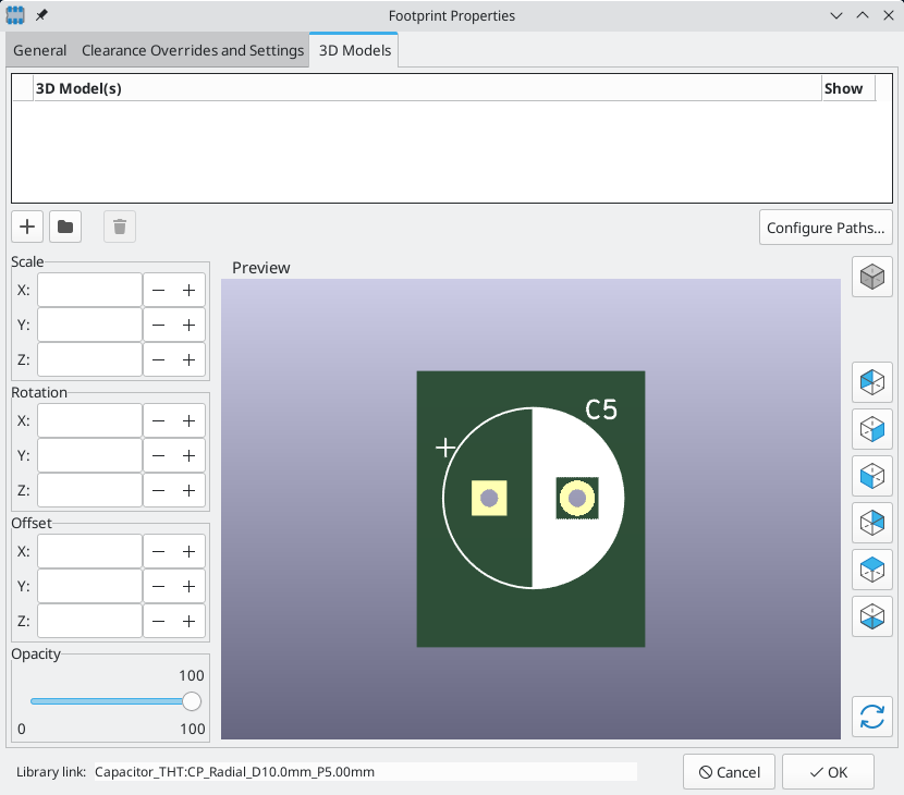
点击 ![]() 按钮,选择 IDF(*.idf;*.IDF) 文件类型筛选器。浏览到所需的边框文件。
按钮,选择 IDF(*.idf;*.IDF) 文件类型筛选器。浏览到所需的边框文件。
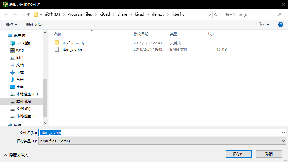
一旦选择了所需的元件边框文件,输入任何必要的偏移和旋转值。偏移量必须使用 IDF 板的输出单位(毫米或密耳)并在 IDF 坐标系中指定,这是一个右手坐标系,+Z 指向观察者,+X 指向观察者的右边,+Y 指向屏幕的上边缘。旋转必须以度为单位;正向旋转是逆时针旋转,如 IDF v3 规范中所述。
多个边框可以与适当的偏移量结合起来,以表示简单的装配,如插座中的 DIP 封装。
| IDF 导出器只使用偏移值和 Z 旋转值,所有其他数值都被忽略。 |
创建元件边框文件
元件边框的创建应该与相应的封装 的方向和位置相匹配。这就避免了为IDF 元件边框指定非零旋转的需要。由于 IDF 导出器忽略了(X,Y)偏移值,所以在 IDF 元件边框中使用正确的原点是至关重要的。
元件边框部分包含字符串,整数或浮点数字段。 字符串是可包含空格的字符组合; 如果字符串包含空格,则必须引用它。 引号不得出现在字符串中。 浮点数可以使用十进制或指数表示法表示,但十进制表示法是人类可读性的首选。 小数点必须是点而不是逗号。 IDF 文件必须只包含7 位 ASCII 字符; 使用8位字符将导致未定义的行为。
IDF 文件由 SECTIONS 组成,SECTIONS 由 RECORDS 组成,RECORDS 由 FIELDS 组成。对于 IDF 边框文件,只有一种类型的部分可以存在,并且必须是 .ELECTRICAL 或 .MECHANICAL 中的一种。一个记录是一行文本,可能包含一个或多个字段。字段是由一个或多个空格分隔的字符序列,不在引号之间出现。一条记录的所有字段必须出现在单行上;记录不能跨行。
节的标题(.ELECTRICAL 或 .MECHANICAL)被认为是该节的第一条记录(记录 1)。记录 1后面必须有记录 2,该记录有四个字:
-
几何名称:与零件号组合的字符串必须形成元件边框的唯一标识符。 对于标准化包,包名称是几何名称的良好值,例如 SOT-23 。 对于独特的包装,制造商的部件号是几何名称的不错选择。
-
部件号:虽然显然是用于部件号,例如 BS107,但最好使用此字符串来帮助描述包。 例如,如果几何名称是 TO-92 ,则部件号条目可用于描述焊盘的布局或该特定 TO-92 边框文件的方向。
-
IDF 单位:这必须是
MM或THOU中的一个,它只适用于描述这个单一成分边框的单位。 -
高度:这是一个浮点数,表示使用字段 3 中指定的单位的元件的标称高度。
记录2后面必须跟有许多记录 3 条目,这些条目指定了元件的边框。 记录 3 包含四个字段:
-
循环索引。
0(边框点按逆时针顺序指定)或1(边框点按顺时针顺序指定)。 -
X 坐标:浮点数
-
Y 坐标:浮点数
-
包括角度:一个浮点数。如果该值为
0,则从上一点到这一点绘制一条直线段。 如果数值是360,那么前一个点指定一个圆的中心,这个点指定圆上的一个点;千万不要用360的数值指定一个圆,因为至少有一个主要的机械 CAD 包在这种情况下表现不好。如果该值为负数,则从上一点到这一点将绘制顺时针方向的圆弧;如果该值为正数,则绘制逆时针方向的圆弧。
只允许一个闭环,并且无法指定切口。 指定的最后一个点必须与第一个点相同,除非边框是圆形。
示例 IDF 文件 1:
# a simple cylinder - this could represent an electrolytic capacitor
.ELECTRICAL
    "cylinder" "5mm OD, 5mm height" MM 5
    0 0 0 0
    0 2.5 0 360
.END_ELECTRICAL
示例 IDF 文件 2:
# an upside-down T
# a comment added for the sake of adding comments
.ELECTRICAL
    "Capital T" "5x8x10mm, upside down" MM 10
    0 -0.5 8 0
    0 -0.5 0.5 0
    0 -2.5 0.5 0
    0 -2.5 -0.5 180
    0 2.5 -0.5 0
    0 2.5 0.5 180
    0 0.5 0.5 0
    0 0.5 8 0
    0 -0.5 8 180
.END_ELECTRICAL
创建边框的准则
在创建边框时,特别是在与他人共享工作时,文件的设计和命名的一致性可以帮助人们更快地找到文件并以最小的麻烦放置元件。
包命名
尝试提供有关文件名中可用边框的一些信息,以便用户大致了解边框是什么。 例如,轴向引线圆柱形封装可能代表某些类型的电容器以及某些类型的电阻,因此将边框识别为水平或垂直轴向引线装置并在相关尺寸上添加一些额外信息是有意义的:直径,长度 和音高是最重要的。 如果设备具有唯一的边框,则制造商的部件号和用于指示设备类别的前缀就足够了。
注释
使用 IDF 文件中的注释为用户提供有关边框的更多信息,例如对用于尺寸信息的源的引用。
几何和部件编号条目
仔细考虑要赋予几何和部件编号条目的值。 总之,这些字符串充当 MCAD 系统的唯一标识符。 理想情况下,字符串的值对用户有一定的意义,但这不是必需的:这些值主要用于 MCAD 系统用作唯一 ID。 理想情况下,所选择的值在任何大型边框集中都是唯一的; 选择好的价值将导致更少的冲突,特别是在复杂的板上。
引脚方向和定位
元件边框的创建应该与相应的封装的方向和位置相匹配。这就避免了为 IDF 元件边框指定非零旋转的需要。由于 IDF 导出器忽略了 (X,Y) 偏移值,所以在 IDF 元件边框中使用正确的原点是至关重要的。
上图显示了由程序 idfcyl 和 idfrect 生成并在一个机械 CAD 程序中渲染的样本边框。从左到右分别是 (a) 垂直径向引线圆柱体,(b) 垂直轴向引线圆柱体,左边有金属丝,(c) 垂直轴向引线圆柱体,右边有金属丝,(d) 水平轴向引线圆柱体,(e) 水平径向引线圆柱体,(f) 方形边框,普通,(g) 方形边框有倒角,(h) 方形边框有轴向引线在右边。上面的边框以毫米为单位,下面的边框以英寸为单位。
尺寸提示
推挤边框的目的是让机械设计者了解每个部件占据的位置和物理空间。在典型情况下,机械设计师将使用更详细的机械模型替换一些原始边框,例如在检查时确保直角安装的 LED 适合面板上的孔。在大多数情况下,边框的准确性无关紧要,但优良作法是创建可传达最佳机械信息的边框。在少数情况下,用户可能希望将元件装配到具有非常小的多余空间的壳体中,例如在便携式音乐播放器中。在这种情况下,如果大多数推挤边框是元件的足够好的表示,那么机械设计师可能只需要在设计壳体时替换很少的模型。如果边框不是现实的可靠反映,那么机械设计师将浪费大量时间来更换模型以确保良好的贴合性。毕竟,如果你把垃圾放进去,你可以期待垃圾出来。如果您提供了良好的信息,您可以对良好的结果充满信心。
IDF 元件边框工具
许多命令行工具可用于帮助生成 IDF 元件边框。 工具是:
-
idfcyl:创建一个垂直或水平方向的圆柱体边框,并具有轴向或径向引线 -
idfrect:创建一个矩形的边框,这个矩形可以有一个轴向引线或左上角的倒角 -
dxf2idf:将 DXF 格式的图纸转换为 IDF 元件边框
idfcyl
idfcyl 生成圆柱形元件的边框。
当 idfcyl 被调用时,没有参数,它会打印出一个使用说明和输入的摘要:
idfcyl:该程序生成圆柱形元件的边框。
     圆筒可以是水平的或垂直的。
     水平圆柱体可以在一端或两端具有线。
     垂直圆柱体可以具有至多一根可以是的线
     放在左侧或右侧。

输入:
    单位:mm, in(毫米或英寸)
    方向:V(垂直)
    引线类型:X,R(轴向,径向)
    体型直径
    体型长度
    板偏移
    *   线径
    *   节距
    **  线侧:L,R(左,右)
    *** 引线长度
    文件名(必须以 * .idf 结尾)

    注意:
         *   仅用于水平方向或
             带轴向引线的垂直方向

        **  只有轴向引线的垂直方向才需要

        ***  仅对于带有径向引线的水平方向需要
可以通过在命令行上输入任意参数来抑制注释。 用户可以在命令行手动输入信息或创建脚本以生成边框。 以下脚本创建一个单个圆柱轴向引线边框,右侧为引线:
#!/bin/bash
# Generate a cylindrical IDF outline for test purposes
# vertical 5mm cylinder,  nominal length 8mm + 3mm board offset,
# axial wire on right,  0.8mm wire dia., 3.5mm pitch
idfcyl - 1 > /dev/null <<  _EOF
mm
v
x
5
8
3
0.8
3.5
r
cylvmm_1R_D5_L8_Z3_WD0.8_P3.5.idf
_EOF
idfrect
idfrect 生成矩形元件的边框。
当 idfrect 被调用而没有参数时,它会打印出使用说明和输入摘要:
idfrect:该程序生成矩形元件的边框。
     该部件可以具有单个引线(轴向)或倒角
     左上角。
输入:
     单位:毫米,英寸(毫米或英寸)
     宽度:
     长度:
     高度:
     倒角:长度为 45 度。倒棱
     * 倾斜的角度:Y,N(引线始终向右边)
     ** 线径
     ** 球场
     文件名(必须以 *.idf 结尾)

    NOTES:
        *   only required if chamfer = 0

        **  仅对倾斜的角度元件有要求
可以通过在命令行上输入任意参数来抑制注释。 用户可以在命令行手动输入信息或创建脚本以生成边框。 以下脚本创建倒角矩形和轴向引线边框:
#!/bin/bash
# Generate various rectangular IDF outlines for test purposes
# 10x10, 1mm chamfer, 2mm height
idfrect - 1 > /dev/null <<  _EOF
mm
10
10
2
1
rectMM_10x10x2_C0.5.idf
_EOF
# 10x10x12,  0.8mm lead on 6mm pitch
idfrect - 1 > /dev/null <<  _EOF
mm
10
10
12
0
Y
0.8
6
rectLMM_10x10x12_D0.8_P6.0.idf
_EOF
dxf2idf
dxf2idf 从 DXF 边框创建一个 IDF 元件文件。
用于指定元件边框的 DXF 文件可以用免费软件 LibreCAD 来准备,以获得最佳的兼容性。
当 dxf2idf 被调用而没有参数时,它会打印出一个使用说明和输入的摘要:
dxf2idf:此程序采用线段,圆弧和圆弧段 从 DXF 文件中创建 IDF 元件边框文件。

输入:
     DXF 文件名:输入文件,必须以 _.dxf_ 结尾
     单位:毫米,英寸(毫米或英寸)
     几何名称:字符串,根据 IDF 3.0版规范
     部件名称:根据部件号的 IDF 3.0版规范
     高度:边框的挤压高度
     注释:所有非空行都是要添加的注释
         IDF 文件。 空行表示结束
         注释块。
     文件名:输出文件名,必须以 _.idf_ 结尾
可以通过在命令行上输入任何任意参数来抑制注释的产生。用户可以在命令行上手动输入信息或创建脚本来生成边框。下面的脚本从 DXF 文件 test.dxf 创建了一个 5 毫米高的边框:
#!/bin/bash
# Generate an IDF outlines from a DXF file
dxf2idf - 1 > /dev/null << _EOF
test.dxf
mm
DXF TEST GEOMETRY
DXF TEST PART
5
This is an IDF test file produced from the outline 'test.dxf'
This is a second IDF comment to demonstrate multiple comments

test_dxf2idf.idf
_EOF
idf2vrml
idf2vrml 工具读取一组 IDF 板(.emn)和一个 IDF 元件文件(.emp)并产生一个 VRML 文件,可以用 VRML 查看器查看。在用户不能使用 MCAD 软件的情况下,这个功能对板件装配的可视化很有用。在没有任何参数的情况下调用 idf2vrml 将导致显示一个使用信息:
>./idf2vrml
用法: idf2vrml -f input_file.emn -s scale_factor {-k} {-d} {-z} {-d} {-z} {-m}
标志:
   -k: 产生 KiCad 友好的 VRML 输出;默认为紧凑的 VRML
   -d: 抑制对默认边框的替换
   -z: 抑制零高度边框的渲染
   -m: 打印对象映射到标准输出用于调试目的。
例子产生一个供 KiCad 使用的模型: idf2vrml -f input.emn -s 0.3937008 -k
idf2vrml 工具不能正确渲染 emn 文件中的 OTHER_OUTLINE 实体,如果该实体被指定在 PCB 的底层;然而你不会注意到使用 KiCad 导出的文件,因为没有机制来指定这样的实体。这只是一个问题,如果你渲染一个第三方的 emn 文件,该文件确实在电路板的底层采用了一个实体。
|
操作参考
下面是 PCB 编辑器中每个可用的 操作 的列表:可以分配给快捷键的命令。
PCB 编辑器
以下动作在 PCB 编辑器中是可用的。快捷键可以分配给偏好设置中的 快捷键 部分的任何操作。
| Action | Default Hotkey | Description |
|---|---|---|
Align to Bottom |
Aligns selected items to the bottom edge |
|
Align to Horizontal Center |
Aligns selected items to the horizontal center |
|
Align to Vertical Center |
Aligns selected items to the vertical center |
|
Align to Left |
Aligns selected items to the left edge |
|
Align to Right |
Aligns selected items to the right edge |
|
Align to Top |
Aligns selected items to the top edge |
|
Distribute Horizontally |
Distributes selected items along the horizontal axis |
|
Distribute Vertically |
Distributes selected items along the vertical axis |
|
Place Off-Board Footprints |
Performs automatic placement of components outside board area |
|
Place Selected Footprints |
Performs automatic placement of selected components |
|
Flip Board View |
View board from the opposite side |
|
Sketch Graphic Items |
Show graphic items in outline mode |
|
Decrease Layer Opacity |
{ |
Make the current layer more transparent |
Increase Layer Opacity |
} |
Make the current layer less transparent |
Switch to Copper (B.Cu) layer |
PgDn |
Switch to Copper (B.Cu) layer |
Switch to Inner layer 1 |
Switch to Inner layer 1 |
|
Switch to Inner layer 10 |
Switch to Inner layer 10 |
|
Switch to Inner layer 11 |
Switch to Inner layer 11 |
|
Switch to Inner layer 12 |
Switch to Inner layer 12 |
|
Switch to Inner layer 13 |
Switch to Inner layer 13 |
|
Switch to Inner layer 14 |
Switch to Inner layer 14 |
|
Switch to Inner layer 15 |
Switch to Inner layer 15 |
|
Switch to Inner layer 16 |
Switch to Inner layer 16 |
|
Switch to Inner layer 17 |
Switch to Inner layer 17 |
|
Switch to Inner layer 18 |
Switch to Inner layer 18 |
|
Switch to Inner layer 19 |
Switch to Inner layer 19 |
|
Switch to Inner layer 2 |
Switch to Inner layer 2 |
|
Switch to Inner layer 20 |
Switch to Inner layer 20 |
|
Switch to Inner layer 21 |
Switch to Inner layer 21 |
|
Switch to Inner layer 22 |
Switch to Inner layer 22 |
|
Switch to Inner layer 23 |
Switch to Inner layer 23 |
|
Switch to Inner layer 24 |
Switch to Inner layer 24 |
|
Switch to Inner layer 25 |
Switch to Inner layer 25 |
|
Switch to Inner layer 26 |
Switch to Inner layer 26 |
|
Switch to Inner layer 27 |
Switch to Inner layer 27 |
|
Switch to Inner layer 28 |
Switch to Inner layer 28 |
|
Switch to Inner layer 29 |
Switch to Inner layer 29 |
|
Switch to Inner layer 3 |
Switch to Inner layer 3 |
|
Switch to Inner layer 30 |
Switch to Inner layer 30 |
|
Switch to Inner layer 4 |
Switch to Inner layer 4 |
|
Switch to Inner layer 5 |
Switch to Inner layer 5 |
|
Switch to Inner layer 6 |
Switch to Inner layer 6 |
|
Switch to Inner layer 7 |
Switch to Inner layer 7 |
|
Switch to Inner layer 8 |
Switch to Inner layer 8 |
|
Switch to Inner layer 9 |
Switch to Inner layer 9 |
|
Switch to Next Layer |
+ |
Switch to Next Layer |
Switch to Previous Layer |
- |
Switch to Previous Layer |
Toggle Layer |
V |
Switch between layers in active layer pair |
Switch to Component (F.Cu) layer |
PgUp |
Switch to Component (F.Cu) layer |
Net Inspector |
Show the net inspector |
|
Local Ratsnest |
Toggle ratsnest display of selected item(s) |
|
Net Color Mode (3-state) |
Cycle between using net and netclass colors for all nets, just ratsnests, and none |
|
Sketch Pads |
Show pads in outline mode |
|
Curved Ratsnest Lines |
Show ratsnest with curved lines |
|
Ratsnest Mode (3-state) |
Cycle between showing ratsnests for all layers, just visible layers, and none |
|
Repair Board |
Run various diagnostics and attempt to repair board |
|
Show Appearance Manager |
Show/hide the appearance manager |
|
Show pad numbers |
Show pad numbers |
|
Show Properties Manager |
Show/hide the properties manager |
|
Scripting Console |
Show the Python scripting console |
|
Show Ratsnest |
Show board ratsnest |
|
Sketch Text Items |
Show footprint texts in line mode |
|
Sketch Tracks |
K |
Show tracks in outline mode |
Sketch Vias |
Show vias in outline mode |
|
Draw Zone Outlines |
Show only zone boundaries |
|
Draw Zone Fills |
Show filled areas of zones |
|
Toggle Zone Display |
Cycle between showing zone fills and just their outlines |
|
Create Arc from Selection |
Creates an arc from the selected line segment |
|
Create Rule Area from Selection… |
Creates a rule area from the selection |
|
Create Lines from Selection |
Creates graphic lines from the selection |
|
Create Polygon from Selection… |
Creates a graphic polygon from the selection |
|
Create Tracks from Selection |
Creates tracks from the selected graphic lines |
|
Create Zone from Selection… |
Creates a copper zone from the selection |
|
Design Rules Checker |
Show the design rules checker window |
|
Open in Footprint Editor |
Ctrl+E |
Opens the selected footprint in the Footprint Editor |
Edit Library Footprint… |
Ctrl+Shift+E |
Opens the selected footprint in the Footprint Editor |
Append Board… |
Open another board and append its contents to this board |
|
Assign Netclass… |
Assign a netclass to nets matching a pattern |
|
Board Setup… |
Edit board setup including layers, design rules and various defaults |
|
Clear Net Highlighting |
~ |
Clear any existing net highlighting |
Drill/Place File Origin |
Place origin point for drill files and component placement files |
|
Export Specctra DSN… |
Export Specctra DSN routing info |
|
BOM… |
Create bill of materials from board |
|
IPC-D-356 Netlist File… |
Generate IPC-D-356 netlist file |
|
Drill Files (.drl)… |
Generate Excellon drill file(s) |
|
Gerbers (.gbr)… |
Generate Gerbers for fabrication |
|
Component Placement (.pos)… |
Generate component placement file(s) for pick and place |
|
Footprint Report (.rpt)… |
Create report of all footprints from current board |
|
Group |
Group the selected items so that they are treated as a single item |
|
Enter Group |
Enter the group to edit items |
|
Leave Group |
Leave the current group |
|
Hide Net in Ratsnest |
Hide the selected net in the ratsnest of unconnected net lines/arcs |
|
Highlight Net |
` |
Highlight net under cursor |
Highlight Net |
Highlight all copper items on the selected net(s) |
|
Import Netlist… |
Read netlist and update board connectivity |
|
Import Specctra Session… |
Import routed Specctra session (*.ses) file |
|
Lock |
Prevent items from being moved and/or resized on the canvas |
|
Add Footprint |
A |
Add a footprint |
Remove Items |
Remove items from group |
|
Switch to Schematic Editor |
Open in schematic editor |
|
Show Net in Ratsnest |
Show the selected net in the ratsnest of unconnected net lines/arcs |
|
Constrain to H, V, 45 |
Shift+Space |
Limit actions to horizontal, vertical, or 45 degrees from the starting point |
Toggle Last Net Highlight |
Toggle between last two highlighted nets |
|
Toggle Lock |
L |
Lock or unlock selected items |
Toggle Net Highlight |
Alt+` |
Toggle net highlighting |
Switch Track Width to Previous |
Shift+W |
Change track width to previous pre-defined size |
Switch Track Width to Next |
W |
Change track width to next pre-defined size |
Ungroup |
Ungroup any selected groups |
|
Unlock |
Allow items to be moved and/or resized on the canvas |
|
Decrease Via Size |
kbd:[\] |
Change via size to previous pre-defined size |
Increase Via Size |
' |
Change via size to next pre-defined size |
Duplicate Zone onto Layer… |
Duplicate zone outline onto a different layer |
|
Merge Zones |
Merge zones |
|
Change Footprint… |
Assign a different footprint from the library |
|
Change Footprints… |
Assign different footprints from the library |
|
Cleanup Graphics… |
Cleanup redundant items, etc. |
|
Cleanup Tracks & Vias… |
Cleanup redundant items, shorting items, etc. |
|
Edit Text & Graphics Properties… |
Edit Text and graphics properties globally across board |
|
Edit Track & Via Properties… |
Edit track and via properties globally across board |
|
Global Deletions… |
Delete tracks, footprints and graphic items from board |
|
Remove Unused Pads… |
Remove or restore the unconnected inner layers on through hole pads and vias |
|
Swap Layers… |
Move tracks or drawings from one layer to another |
|
Update Footprint… |
Update footprint to include any changes from the library |
|
Update Footprints from Library… |
Update footprints to include any changes from the library |
|
Clearance Resolution… |
Show clearance resolution for the active layer between two selected objects |
|
Constraints Resolution… |
Show constraints resolution for the selected object |
|
Show Board Statistics |
Shows board statistics |
|
Add Aligned Dimension |
Ctrl+Shift+H |
Add an aligned linear dimension |
Draw Arc |
Ctrl+Shift+A |
Draw an arc |
Switch Arc Posture |
/ |
Switch the arc posture |
Add Center Dimension |
Add a center dimension |
|
Draw Circle |
Ctrl+Shift+C |
Draw a circle |
Close Outline |
Close the in progress outline |
|
Decrease Line Width |
Ctrl+- |
Decrease the line width |
Delete Last Point |
Back |
Delete the last point added to the current item |
Draw Graphic Polygon |
Ctrl+Shift+P |
Draw a graphic polygon |
Increase Line Width |
Ctrl++ |
Increase the line width |
Add Leader |
Add a leader dimension |
|
Draw Line |
Ctrl+Shift+L |
Draw a line |
Add Orthogonal Dimension |
Add an orthogonal dimension |
|
Add Board Characteristics |
Add a board characteristics table on a graphic layer |
|
Add Image |
Add bitmap image |
|
Import Graphics… |
Ctrl+Shift+F |
Import 2D drawing file |
Add Stackup Table |
Add a board stackup table on a graphic layer |
|
Add Radial Dimension |
Add a radial dimension |
|
Draw Rectangle |
Draw a rectangle |
|
Add Rule Area |
Ctrl+Shift+K |
Add a rule area (keepout) |
Place the Footprint Anchor |
Ctrl+Shift+N |
Set the coordinate origin point (anchor) of the footprint |
Add a Similar Zone |
Ctrl+Shift+. |
Add a zone with the same settings as an existing zone |
Add Text |
Ctrl+Shift+T |
Add a text item |
Add Text Box |
Add a wrapped text item |
|
Add Vias |
Ctrl+Shift+V |
Add free-standing vias |
Add Filled Zone |
Ctrl+Shift+Z |
Add a filled zone |
Add a Zone Cutout |
Shift+C |
Add a cutout area of an existing zone |
Get and Move Footprint |
T |
Selects a footprint by reference designator and places it under the cursor for moving |
Change Track Width |
Updates selected track & via sizes |
|
Create Array… |
Ctrl+T |
Create array |
Delete Full Track |
Shift+Del |
Deletes selected item(s) and copper connections |
Duplicate and Increment |
Ctrl+Shift+D |
Duplicates the selected item(s), incrementing pad numbers |
Fillet Lines |
Adds arcs tangent to the selected lines |
|
Fillet Tracks |
Adds arcs tangent to the selected straight track segments |
|
Change Side / Flip |
F |
Flips selected item(s) to opposite side of board |
Mirror Horizontally |
Mirrors selected item across the Y axis |
|
Mirror Vertically |
Mirrors selected item across the X axis |
|
Move Exactly… |
Shift+M |
Moves the selected item(s) by an exact amount |
Pack and Move Footprints |
P |
Sorts selected footprints by reference, packs based on size and initiates movement |
Properties… |
E |
Displays item properties dialog |
Rotate Counterclockwise |
R |
Rotates selected item(s) counterclockwise |
Rotate Clockwise |
Shift+R |
Rotates selected item(s) clockwise |
Skip |
Tab |
Skip item |
Swap |
Shift+S |
Swaps selected items' positions |
Copy with Reference |
Copy selected item(s) to clipboard with a specified starting point |
|
Move |
M |
Moves the selected item(s) |
Move Individually |
Ctrl+M |
Moves the selected items one-by-one |
Move with Reference |
Moves the selected item(s) with a specified starting point |
|
Attempt Finish |
F |
Attempts to complete current route to nearest ratsnest end. |
Attempt Finish Selected (Autoroute) |
Shift+F |
Sequentially attempt to automatically route all selected pads. |
Break Track |
Splits the track segment into two segments connected at the cursor position. |
|
Route From Other End |
E |
Commits current segments and starts next segment from nearest ratsnest end. |
Custom Track/Via Size… |
Q |
Shows a dialog for changing the track width and via size. |
Cycle Router Mode |
Cycle router to the next mode |
|
Route Differential Pair |
6 |
Route differential pairs |
Differential Pair Dimensions… |
Open Differential Pair Dimension settings |
|
Drag (45 degree mode) |
D |
Drags the track segment while keeping connected tracks at 45 degrees. |
Drag (free angle) |
G |
Drags the nearest joint in the track without restricting the track angle. |
Finish Track |
End |
Stops laying the current track. |
Router Highlight Mode |
Switch router to highlight mode |
|
Place Blind/Buried Via |
Alt+Shift+V |
Adds a blind or buried via at the end of currently routed track. |
Place Microvia |
Ctrl+V |
Adds a microvia at the end of currently routed track. |
Place Through Via |
V |
Adds a through-hole via at the end of currently routed track. |
Route Selected |
Shift+X |
Sequentially route selected items from ratsnest anchor. |
Route Selected From Other End |
Shift+E |
Sequentially route selected items from other end of ratsnest anchor. |
Select Layer and Place Blind/Buried Via… |
Alt+< |
Select a layer, then add a blind or buried via at the end of currently routed track. |
Select Layer and Place Micro Via… |
Select a layer, then add a micro via at the end of currently routed track. |
|
Select Layer and Place Through Via… |
< |
Select a layer, then add a through-hole via at the end of currently routed track. |
Set Layer Pair… |
Change active layer pair for routing |
|
Interactive Router Settings… |
Ctrl+< |
Open Interactive Router settings |
Router Shove Mode |
Switch router to shove mode |
|
Route Single Track |
X |
Route tracks |
Switch Track Posture |
/ |
Switches posture of the currently routed track. |
Track Corner Mode |
Ctrl+/ |
Switches between sharp/rounded and 45°/90° corners when routing tracks. |
Undo Last Segment |
Back |
Walks the current track back one segment. |
Router Walkaround Mode |
Switch router to walkaround mode |
|
Deselect All Tracks in Net |
Deselects all tracks & vias belonging to the same net. |
|
Filter Selected Items… |
Remove items from the selection by type |
|
Grab Nearest Unconnected Footprints |
Shift+O |
Selects and initiates moving the nearest unconnected footprint on each selected net. |
Select/Expand Connection |
U |
Selects a connection or expands an existing selection to junctions, pads, or entire connections |
Select All Tracks in Net |
Selects all tracks & vias belonging to the same net. |
|
Select on Schematic |
Selects corresponding items in Schematic editor |
|
Sheet |
Selects all footprints and tracks in the schematic sheet |
|
Items in Same Hierarchical Sheet |
Selects all footprints and tracks in the same schematic sheet |
|
Select All Unconnected Footprints |
O |
Selects all unconnected footprints belonging to each selected net. |
Unroute Selected |
Unroutes selected items to the nearest pad. |
|
Decrease Amplitude |
4 |
Decrease meander amplitude by one step. |
Increase Amplitude |
3 |
Increase meander amplitude by one step. |
End Track |
End |
Stops laying the current meander. |
Length Tuning Settings… |
Ctrl+L |
Sets the length tuning parameters for currently routed item. |
Decrease Spacing |
2 |
Decrease meander spacing by one step. |
Increase Spacing |
1 |
Increase meander spacing by one step. |
New Track |
X |
Starts laying a new track. |
Tune length of a differential pair |
8 |
Tune length of a differential pair |
Tune skew of a differential pair |
9 |
Tune skew of a differential pair |
Tune length of a single track |
7 |
Tune length of a single track |
Add Microwave Polygonal Shape |
Create a microwave polygonal shape from a list of vertices |
|
Add Microwave Gap |
Create gap of specified length for microwave applications |
|
Add Microwave Line |
Create line of specified length for microwave applications |
|
Add Microwave Stub |
Create stub of specified length for microwave applications |
|
Add Microwave Arc Stub |
Create stub (arc) of specified size for microwave applications |
|
Footprint Checker |
Show the footprint checker window |
|
Copy Footprint |
Copy Footprint |
|
Create Footprint… |
Create a new footprint using the Footprint Wizard |
|
Cut Footprint |
Cut Footprint |
|
Delete Footprint from Library |
Delete Footprint from Library |
|
Duplicate Footprint |
Make a copy of the selected footprint |
|
Edit Footprint |
Show selected footprint on editor canvas |
|
Export Footprint… |
Export footprint to file |
|
Footprint Properties… |
Edit footprint properties |
|
Hide Footprint Tree |
Hide Footprint Tree |
|
Import Footprint… |
Import footprint from file |
|
New Footprint… |
Ctrl+N |
Create a new, empty footprint |
Paste Footprint |
Paste Footprint |
|
Rename Footprint… |
Rename the selected footprint |
|
Repair Footprint |
Run various diagnostics and attempt to repair footprint |
|
Show Footprint Tree |
Show Footprint Tree |
|
Paste Default Pad Properties to Selected |
Replace the current pad’s properties with those copied earlier |
|
Copy Pad Properties to Default |
Copy current pad’s properties |
|
Push Pad Properties to Other Pads… |
Copy the current pad’s properties to other pads |
|
Default Pad Properties… |
Edit the pad properties used when creating new pads |
|
Renumber Pads… |
Renumber pads by clicking on them in the desired order |
|
Edit Pad as Graphic Shapes |
Ctrl+E |
Ungroups a custom-shaped pad for editing as individual graphic shapes |
Add Pad |
Add a pad |
|
Finish Pad Edit |
Ctrl+E |
Regroups all touching graphic shapes into the edited pad |
Create Corner |
Ins |
Create a corner |
Keep arc center, adjust radius |
Switch arc editing mode to keep center, adjust radius and endpoints |
|
Keep arc endpoints or direction of starting point |
Switch arc editing mode to keep endpoints, or to keep direction of the other point |
|
Remove Corner |
Remove corner |
|
Position Relative To… |
Shift+P |
Positions the selected item(s) by an exact amount relative to another |
Geographical Reannotate… |
Reannotate PCB in geographical order |
|
Refresh Plugins |
Reload all python plugins and refresh plugin menus |
|
Open Plugin Directory |
Opens the directory in the default system file manager |
|
Draft Fill Selected Zone(s) |
Update copper fill of selected zone(s) without regard to other interacting zones |
|
Fill All Zones |
B |
Update copper fill of all zones |
Unfill Selected Zone(s) |
Remove copper fill from selected zone(s) |
|
Unfill All Zones |
Ctrl+B |
Remove copper fill from all zones |
3D 查看器
以下动作可在 3D 浏览器中使用。快捷键可以分配给偏好设置中的 快捷键 部分的任何这些操作。
| Action | Default Hotkey | Description |
|---|---|---|
Toggle 3D models not in pos file |
P |
Toggle 3D models not in pos file |
Toggle unspecified 3D models |
V |
Toggle 3D models for 'unspecified' type components |
Toggle SMD 3D models |
S |
Toggle 3D models for 'Surface mount' type components |
Toggle Through Hole 3D models |
T |
Toggle 3D models for 'Through hole' type components |
Flip Board |
F |
Flip the board view |
Home view |
Home |
Home view |
Render CAD Colors |
Use a CAD color style based on the diffuse color of the material |
|
Render Solid Colors |
Use only the diffuse color property from model 3D model file |
|
Render Realistic Materials |
Use all material properties from each 3D model file |
|
Move board Down |
Down |
Move board Down |
Move board Left |
Left |
Move board Left |
Move board Right |
Right |
Move board Right |
Move board Up |
Up |
Move board Up |
No 3D Grid |
No 3D Grid |
|
Center pivot rotation |
Space |
Center pivot rotation (middle mouse click) |
Reset view |
R |
Reset view |
Rotate X Clockwise |
Rotate X Clockwise |
|
Rotate X Counterclockwise |
Rotate X Counterclockwise |
|
Rotate Y Clockwise |
Rotate Y Clockwise |
|
Rotate Y Counterclockwise |
Rotate Y Counterclockwise |
|
Rotate Z Clockwise |
Rotate Z Clockwise |
|
Rotate Z Counterclockwise |
Rotate Z Counterclockwise |
|
3D Grid 10mm |
3D Grid 10mm |
|
3D Grid 1mm |
3D Grid 1mm |
|
3D Grid 2.5mm |
3D Grid 2.5mm |
|
3D Grid 5mm |
3D Grid 5mm |
|
Show 3D Axis |
Show 3D Axis |
|
Show Model Bounding Boxes |
Show Model Bounding Boxes |
|
Toggle adhesive display |
Toggle display of adhesive layers |
|
Toggle board body display |
Toggle board body display |
|
Toggle comments display |
Toggle display of comments and drawings layers |
|
Toggle ECO display |
Toggle display of ECO layers |
|
Toggle orthographic projection |
Enable/disable orthographic projection |
|
Toggle realistic mode |
Toggle realistic mode |
|
Toggle silkscreen display |
Toggle display of silkscreen layers |
|
Toggle solder mask display |
Toggle display of solder mask layers |
|
Toggle solder paste display |
Toggle display of solder paste layers |
|
Toggle zone display |
Toggle zone display |
|
View Back |
Shift+Y |
View Back |
View Bottom |
Shift+Z |
View Bottom |
View Front |
Y |
View Front |
View Left |
Shift+X |
View Left |
View Right |
X |
View Right |
View Top |
Z |
View Top |
通用
以下操作在整个 KiCad 中都可用,包括在 PCB 编辑器中。快捷键可以分配给偏好设置中的 快捷键 部分的任何操作。
| Action | Default Hotkey | Description |
|---|---|---|
Exclude Marker |
Mark current violation in Checker window as an exclusion |
|
Next Marker |
Go to next marker in Checker window |
|
Previous Marker |
Go to previous marker in Checker window |
|
Add Library… |
Add an existing library folder |
|
Click |
Return |
Performs left mouse button click |
Double-click |
End |
Performs left mouse button double-click |
Cursor Down |
Down |
|
Cursor Down Fast |
Ctrl+Down |
|
Cursor Left |
Left |
|
Cursor Left Fast |
Ctrl+Left |
|
Cursor Right |
Right |
|
Cursor Right Fast |
Ctrl+Right |
|
Cursor Up |
Up |
|
Cursor Up Fast |
Ctrl+Up |
|
Switch to Fast Grid 1 |
Alt+1 |
|
Switch to Fast Grid 2 |
Alt+2 |
|
Switch to Next Grid |
N |
|
Switch to Previous Grid |
Shift+N |
|
Grid Properties… |
Set grid dimensions |
|
Reset Grid Origin |
Z |
|
Grid Origin |
S |
Set the grid origin point |
Inactive Layer View Mode |
Toggle inactive layers between normal and dimmed |
|
Inactive Layer View Mode (3-state) |
H |
Cycle inactive layers between normal, dimmed, and hidden |
Inches |
Use inches |
|
Millimeters |
Use millimeters |
|
Mils |
Use mils |
|
New… |
Ctrl+N |
Create a new document in the editor |
New Library… |
Create a new library folder |
|
Open… |
Ctrl+O |
Open existing document |
Page Settings… |
Settings for paper size and title block info |
|
Pan Down |
Shift+Down |
|
Pan Left |
Shift+Left |
|
Pan Right |
Shift+Right |
|
Pan Up |
Shift+Up |
|
Pin Library |
Keep the library at the top of the list |
|
Plot… |
Plot |
|
Print… |
Ctrl+P |
|
Quit |
Close the current editor |
|
Reset Local Coordinates |
Space |
|
Revert |
Throw away changes |
|
Save |
Ctrl+S |
Save changes |
Save All |
Save all changes |
|
Save As… |
Ctrl+Shift+S |
Save current document to another location |
Save a Copy… |
Save a copy of the current document to another location |
|
Select Columns |
||
3D Viewer |
Alt+3 |
Show 3D viewer window |
Show Context Menu |
Perform the right-mouse-button action |
|
Footprint Library Browser |
Browse footprint libraries |
|
Footprint Editor |
Create, delete and edit footprints |
|
Symbol Library Browser |
Browse symbol libraries |
|
Symbol Editor |
Create, delete and edit symbols |
|
Draw Bounding Boxes |
Draw Bounding Boxes |
|
Always Show Cursor |
Ctrl+Shift+X |
Display crosshairs even in selection tool |
Full-Window Crosshairs |
Switch display of full-window crosshairs |
|
Show Grid |
Display background grid in the edit window |
|
Polar Coordinates |
Switch between polar and cartesian coordinate systems |
|
Switch units |
Ctrl+U |
Switch between imperial and metric units |
Unpin Library |
No longer keep the library at the top of the list |
|
Update PCB from Schematic… |
F8 |
Update PCB with changes made to schematic |
Update Schematic from PCB… |
Update schematic with changes made to PCB |
|
Center on Cursor |
F4 |
Center on Cursor |
Zoom to Objects |
Ctrl+Home |
Zoom to Objects |
Zoom to Fit |
Home |
Zoom to Fit |
Zoom In at Cursor |
F1 |
Zoom In at Cursor |
Zoom In |
Zoom In |
|
Zoom Out at Cursor |
F2 |
Zoom Out at Cursor |
Zoom Out |
Zoom Out |
|
Refresh |
F5 |
Refresh |
Zoom to Selection |
Ctrl+F5 |
Zoom to Selection |
Cancel |
Cancel current tool |
|
Copy |
Ctrl+C |
Copy selected item(s) to clipboard |
Cut |
Ctrl+X |
Cut selected item(s) to clipboard |
Cycle arc editing mode |
Ctrl+Space |
Switch to a different method of editing arcs |
Delete |
Del |
Deletes selected item(s) |
Interactive Delete Tool |
Delete clicked items |
|
Duplicate |
Ctrl+D |
Duplicates the selected item(s) |
Find |
Ctrl+F |
Find text |
Find and Replace |
Ctrl+Alt+F |
Find and replace text |
Find Next |
F3 |
Find next match |
Find Next Marker |
Shift+F3 |
|
Paste |
Ctrl+V |
Paste item(s) from clipboard |
Paste Special… |
Paste item(s) from clipboard with annotation options |
|
Redo |
Ctrl+Y |
Redo last edit |
Replace All |
Replace all matches |
|
Replace and Find Next |
Replace current match and find next |
|
Show Search Panel |
Ctrl+G |
Show/hide the search panel |
Select All |
Ctrl+A |
Select all items on screen |
Undo |
Ctrl+Z |
Undo last edit |
Measure Tool |
Ctrl+Shift+M |
Interactively measure distance between points |
Select item(s) |
Select item(s) |
|
Configure Paths… |
Edit path configuration environment variables |
|
Donate |
Open "Donate to KiCad" in a web browser |
|
Get Involved |
Open "Contribute to KiCad" in a web browser |
|
Getting Started with KiCad |
Open “Getting Started in KiCad” guide for beginners |
|
Help |
Open product documentation in a web browser |
|
List Hotkeys… |
Ctrl+F1 |
Displays current hotkeys table and corresponding commands |
Preferences… |
Ctrl+, |
Show preferences for all open tools |
Report Bug |
Report a problem with KiCad |
|
Manage Footprint Libraries… |
Edit the global and project footprint library lists |
|
Manage Symbol Libraries… |
Edit the global and project symbol library lists |