Reference manual
| This manual is in the process of being revised to cover the latest stable release version of KiCad. It contains some sections that have not yet been completed. We ask for your patience while our volunteer technical writers work on this task, and we welcome new contributors who would like to help make KiCad’s documentation better than ever. |
Copyright
This document is Copyright © 2010-2024 by its contributors as listed below. You may distribute it and/or modify it under the terms of either the GNU General Public License (http://www.gnu.org/licenses/gpl.html), version 3 or later, or the Creative Commons Attribution License (http://creativecommons.org/licenses/by/3.0/), version 3.0 or later.
All trademarks within this guide belong to their legitimate owners.
Contributors
Jean-Pierre Charras, Fabrizio Tappero, Wayne Stambaugh, Cirilo Bernardo, Jon Evans, Graham Keeth
Feedback
The KiCad project welcomes feedback, bug reports, and suggestions related to the software or its documentation. For more information on how to sumbit feedback or report an issue, please see the instructions at https://www.kicad.org/help/report-an-issue/
Introduction to the KiCad PCB Editor
Initial configuration
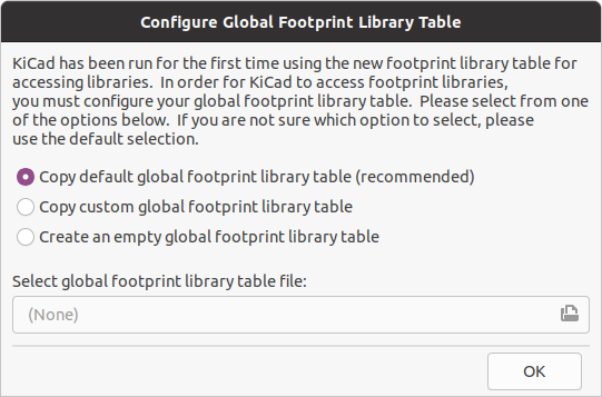
When the PCB Editor is run for the first time, if the global footprint table file fp-lib-table is not
found in the KiCad configuration folder then the KiCad will ask how to create this file:
The first option is recommended (Copy default global footprint library table (recommended)). The default footprint library table includes all of the standard footprint libraries that are installed as part of KiCad.
If this option is disabled, KiCad was unable to find the default global footprint library table. This probably means you did not install the standard footprint libraries with KiCad, or they are not installed where KiCad expects to find them. On some systems the KiCad libraries are installed as a separate package.
-
If you have installed the standard KiCad footprint libraries and want to use them, but the first option is disabled, select the second option and browse to the
fp-lib-tablefile in the directory where the KiCad libraries were installed. -
If you already have a custom footprint library table that you would like to use, select the second option and browse to your
fp-lib-tablefile. -
If you want to construct a new footprint library table from scratch, select the third option.
Footprint library management is described in more detail later.
The PCB Editor user interface
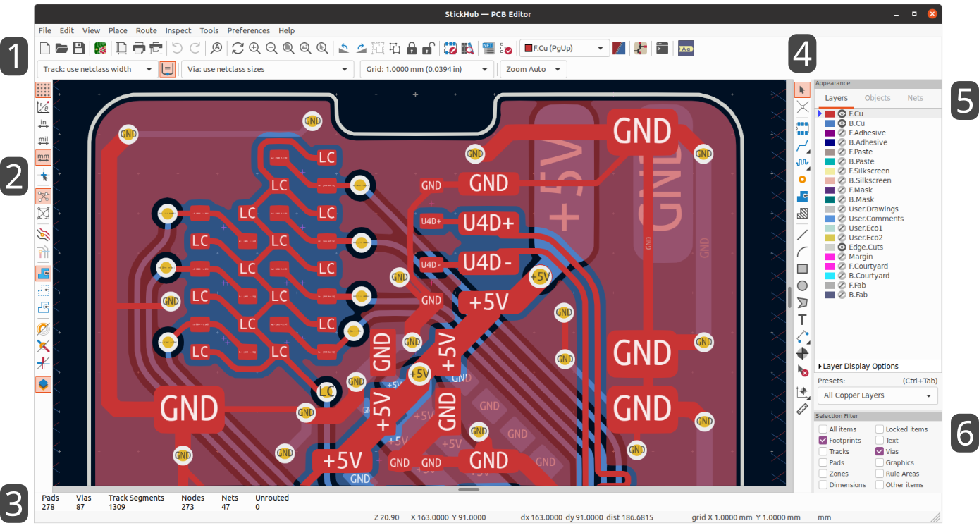
The main PCB Editor user interface is shown above, with some key elements indicated:
-
Top toolbars (file management, zoom tools, editing tools)
-
Left toolbar (display options)
-
Message panel and status bar
-
Right toolbar (drawing and design tools)
-
Appearance panel
-
Selection filter panel
Navigating the editing canvas
The editing canvas is a view onto the board being designed. You can pan and zoom to different areas of the board, and also flip the view to show the board from the bottom.
By default, dragging with the middle or right mouse button will pan the canvas view and scrolling the mouse wheel will zoom the view in or out. You can change this behavior in the Mouse and Touchpad section of the preferences (see Configuration and Customization for details).
Several other zoom tools are available in the top toolbar:
-
 zooms in on the center of the
viewport.
zooms in on the center of the
viewport. -
 zooms out from the center of
the viewport.
zooms out from the center of
the viewport. -
 zooms to fit the
frame around the drawing sheet.
zooms to fit the
frame around the drawing sheet. -
 zooms to
fit the items within the drawing sheet.
zooms to
fit the items within the drawing sheet. -
 allows you to
draw a box to determine the zoomed area.
allows you to
draw a box to determine the zoomed area.
The cursor’s current position is displayed at the bottom of the window (X and Y), along with the current zoom factor (Z), the cursor’s relative position (dx, dy, and dist), the grid setting, and the display units.
The relative coordinates can be reset to zero by pressing Space. This is useful for measuring distance between two points or aligning objects.
Hotkeys
The Ctrl+F1 shortcut displays the current hotkey list. The default hotkey list is included in the Actions Reference section of the manual.
The hotkeys described in this manual use the key labels that appear on a standard PC keyboard. On an Apple keyboard layout, use the Cmd key in place of Ctrl, and the Option key in place of Alt.
Many actions do not have hotkeys assigned by default, but hotkeys can be assigned or redefined using the hotkey editor (Preferences → Preferences… → Hotkeys).
| Many of the actions available through hotkeys are also available in context menus. To access the context menu, right-click in the editing canvas. Different actions will be available depending on what is selected or what tool is active. |
Hotkeys are stored in the file user.hotkeys in KiCad’s configuration
directory. The location is platform-specific:
-
Windows:
%APPDATA%\kicad\7.0\user.hotkeys -
Linux:
~/.config/kicad/7.0/user.hotkeys -
macOS:
~/Library/Preferences/kicad/7.0/user.hotkeys
KiCad can import hotkey settings from a user.hotkeys file using the Import
Hotkeys button in the hotkey editor.
Display and selection controls
Board layers
Layers in the PCB Editor represent physical copper layers on a board, as well as graphical layers used for defining things such as silkscreen, solder mask, and the board edge. There is always one layer that is active in the editor. The active layer is drawn on top of other layers and will be the layer assigned to newly-created objects. The active layer is indicated in the layer selector drop-down box in the top toolbar and is also highlighted in the appearance panel. To change the active layer, you can left-click a layer name in the appearance panel, use the drop-down layer selector in the top toolbar, or use a hotkey. Layers can be hidden to simplify the board view. You can hide a layer even if it is the active layer.
Display order for board layers
| TODO: Explain this. |
The appearance panel
The appearance panel provides controls to manage the visibility, color, and opacity of objects in the PCB Editor’s drawing canvas. It has three tabs: the Layers tab contains controls for the board layers, the Objects tab contains controls for different types of graphical objects, and the Nets tab contains controls for the appearance of the ratsnest and copper items.
Layer controls
In the Layers tab of the appearance panel, each board layer is shown with its color and visibility state. The active layer is shown highlighted with an arrow indicator to the left of the color swatch. Left-click on a layer to choose it as the active layer. Left-click on the corresponding visibility icon to toggle the layer between visible and hidden. Double-click or middle-click on the color swatch to change the layer’s color.
| You must first create a custom color theme in Preferences before you can change layer colors in the appearance panel. |
Below the list of layers is an expandable panel that contains layer display options. The first setting controls how non-active layers are displayed: normal, dimmed, or hidden. The layer display mode can be used to simplify the view and focus on a single layer. Items on inactive layers cannot be selected when the non-active layer display mode is "Dim" or "Hide". You can use the hotkey Ctrl+H to cycle through these display modes quickly.
Flip board view will show the board as if you are looking from the bottom (that is, mirrored around the Y-axis). This option is also available in the View menu.
| Flipping the board view does not change the visual layer ordering, the active layer will remain in front followed by the other layers in their normal order. |
Object controls
The Objects tab of the appearance panel is similar to the Layers tab. The main differences are that some objects have no color setting and that four types of objects (tracks, vias, pads, and zones) have opacity control sliders. The opacity setting here will be multiplied with any opacity set in the layer colors. By default, all objects are fully opaque except for zones, which are set to translucent in order to make it easier to see objects through filled zone areas.
Layer presets
Layer presets store which layers and objects are visible and hidden for easy recall. There are several built-in layer presets and you can save your own custom presets. Custom presets are stored in the project settings for a board, as presets may be specific to a certain board stackup.
To load a preset, choose it from the Presets drop-down menu at the bottom of the appearance panel or use the quick switcher by holding down Ctrl and pressing Tab. Once the quick switcher window appears, you can press Tab and Shift+Tab to cycle through the available presets. When you let go of the Ctrl key, the highlighted preset will be loaded.
To save a custom preset, first use the visibility controls to choose which layers you want visible, then choose Save Preset… from the Presets drop-down menu. Give your preset a name and it will now be available via the drop-down menu and the quick switcher. To modify a custom preset, follow the same process and save the modified version with the same name to overwrite the existing version. To delete a custom preset, choose the Delete Preset… option from the drop-down menu and select the preset to be deleted from the list.
Net and net class controls
The Nets tab of the appearance panel shows a list of all nets and net classes in the board. Each net has a visibility control that controls the visibility of that net in the ratsnest. Hiding nets in the ratsnest does not change the connectivity of the board and will not impact the design rule checker; it only is intended to make the ratsnest easier to understand.
Each net and net class can also have a color assigned. By default, this color applies to the ratsnest lines for the net (or for all the nets in the net class). Nets have no color by default; this is indicated by a checkerboard pattern in the color swatch. Double-click or right-click a net or net class color swatch to set the color.
| The Default net class cannot have a color assigned, as nets in this class will just use the default ratsnest color defined by the color theme. |
You can also select and highlight nets and net classes via the appearance panel: right-click on a net or net class to show these options in a menu.
Below the list of net classes is an expandable panel that contains net display options. The first option controls how net colors are applied. When "All" is selected, all copper items (pads, tracks, vias, and zones) belonging to a net or net class will take on the chosen color. When "Ratsnest" is selected (the default value), only the ratsnest is affected by net and net class colors. When "None" is selected, net and net class colors are ignored.
The second option controls how ratsnest lines are drawn. "All layers" means that ratsnest lines will be drawn between all unconnected items. "Visible layers" means that no ratsnest lines will be drawn to items that are on hidden layers, even when those items are unconnected.
Selection and the selection filter
Selecting items in the editing canvas is done with the left mouse button. Single-clicking on an object will select it and dragging will perform a box selection. A box selection from left to right will only select items that are fully inside the box. A box selection from right to left will select any items that touch the box. A left-to-right selection box is drawn in yellow, with a cursor that indicates exclusive selection, and a right-to-left selection box is drawn in blue with a cursor that indicates inclusive selection.
The selection action can be modified by holding modifier keys while clicking or dragging. The following modifier keys apply when clicking to select single items:
| Modifier Keys (Windows) | Modifier Keys (Linux) | Modifier Keys (macOS) | Selection Effect |
|---|---|---|---|
Ctrl |
Ctrl |
Cmd |
Toggle selection. Note: Ctrl+click can be remapped to highlight net in Preferences → PCB Editor → Editing Options. |
Shift |
Shift |
Shift |
Add the item to the existing selection. |
Ctrl+Shift |
Ctrl+Shift |
Cmd+Shift |
Remove the item from the existing selection. |
long click |
long click or Alt |
long click or Option |
Clarify selection from a pop-up menu. |
The following modifier keys apply when dragging to perform a box selection:
| Modifier Keys (Windows) | Modifier Keys (Linux) | Modifier Keys (macOS) | Selection Effect |
|---|---|---|---|
Ctrl |
Ctrl |
Cmd |
Toggle selection. |
Shift |
Shift |
Shift |
Add item(s) to the existing selection. |
Ctrl+Shift |
Ctrl+Shift |
Cmd+Shift |
Remove item(s) from the existing selection. |
The selection filter panel in the lower right corner of the PCB Editor window controls which types of objects can be selected with the mouse. Turning off selection of unwanted object types makes it easier to select items in a dense board. The "All items" checkbox is a shortcut to turn the other items on and off. The "Locked items" checkbox is independent of the rest, and controls whether or not items that have been locked can be selected. You can right-click any object type in the selection filter to quickly change the filter to only allow selecting that type of object.
When a connected copper item is selected, you can expand the selection to other copper items of the same net using the Expand Selection command in the right-click context menu or with the hotkey U. The first time you run this command, the selection will be expanded to the nearest pad. The second time, the selection will be expanded to all connected items on all layers.
Selecting an object displays information about the object in the message panel at the bottom of the window. Double-clicking an object opens a window to edit the object’s properties.
Pressing Esc will always cancel the current tool or operation and return to the selection tool. Pressing Esc while the selection tool is active will clear the current selection.
Net highlighting
An electrical net (or set of nets) can be highlighted in the PCB editor to visualize how the net is routed across the PCB. Net highlighting can be activated by selecting the net to highlight in the PCB editor or by selecting the corresponding net in the schematic editor when cross-probe highlighting is enabled (see below). When net highlighting is active, the highlighted net or nets will be shown in a brighter color and all other items will be shown in a dimmer color than normal.
There are three ways to select a net or nets to highlight in the PCB editor: by using the hotkey ` after selecting a copper object, by using the context menu of any copper object, and the context menu of the Nets tab of the Appearance panel. When you press the Highlight Net hotkey, the nets of any selected copper items will be highlighted. If no copper items are selected, the net of the copper item under the editor cursor will be highlighted.
Net highlighting can be cleared by using the Clear Net Highlight action (hotkey ~) or by using the Highlight net tool on an empty region in the schematic. By default, Esc also clears net highlighting, but this can be disabled if desired in Preferences → PCB Editor → Editing Options.
When a net or nets have been selected for highlighting, the Toggle Net Highlighting action becomes enabled on the left toolbar (also accessible by hotkey, Ctrl+`). This action will turn the highlighting display on or off without choosing a new net to highlight.
Cross-probing from the schematic
KiCad allows bi-directional cross-probing between the schematic and the PCB. There are several different types of cross-probing.
Selection cross-probing allows you to select a symbol or pin in the schematic to select the corresponding footprint or pad in the PCB (if one exists) and vice-versa. By default, cross-probing will result in the display centering on the cross-probed item and zooming to fit. This behavior can be disabled in the Display Options section of the Preferences dialog.
Highlight cross-probing allows you to highlight a net in the schematic and PCB at the same time. If the option "Highlight cross-probed nets" is enabled in the Display Options section of the Preferences dialog, highlighting a net or bus in the schematic editor will cause the corresponding net or nets to be highlighted in the PCB editor.
Left toolbar display controls
The left toolbar provides options to change the display of items in the PCB Editor.
|
Turns grid display on/off. Note: by default, hiding the grid will disable grid snapping. This behavior can be changed in the Display Options section of Preferences. |
|
Switch between polar and Cartesian coordinate display in the status bar. |
|
Display/entry of coordinates and dimensions in inches, mils, or millimeters. |
|
Switches between full-screen and small editing cursor (crosshairs). |
|
Turns the ratsnest display on/off. |
|
Switches between straight and curved ratsnest lines. |
|
Switches the non-active layer display mode between Normal and Dim. Note: this button will be highlighted when the non-active layer display mode is either Dim or Hide. In both cases, pressing the button will change the layer display mode to Normal. The Hide mode can only be accessed via the controls in the Appearance Panel or via the hotkey Ctrl+H. |
|
When a net has been selected for highlighting, switches the highlighting on or off. Note: this button will be disabled when no net has been highlighted. To highlight a net, use the hotkey `, right-click any copper object in the net and choose Highlight Net from the Net Tools menu, or right-click the net in the list in the Nets tab of the Appearance panel. |
|
Show zone filled areas. |
|
Show zone outlines only. |
|
Switches display of pads between filled and outline mode. |
|
Switches display of vias between filled and outline mode. |
|
Switches display of tracks between filled and outline mode. |
|
Shows or hides the Appearance and Selection Filter panels on the right side of the editor. |
|
Shows or hides the Properties Manager panel on the left side of the editor. |
Creating a PCB
Basic PCB concepts
A printed circuit board in KiCad is generally made up of footprints representing electronic components and their pads, nets defining how those pads connect to each other, tracks, vias, and filled zones that form the copper connections between pads in each net, and various graphic shapes defining the board edge, silkscreen markings, and any other desired information.
KiCad normally keeps the information about nets on a PCB synchronized with an associated schematic, but nets can also be created and edited directly within the PCB editor.
Capabilities
KiCad is capable of creating printed circuit boards with up to 32 copper layers, 14 technical layers (silkscreen, solder mask, component adhesive, solder paste, etc), and 13 general-purpose drawing layers.
The internal measurement resolution of all objects in KiCad is 1 nanometer, and measurements are stored as 32-bit integers. This means it is possible to create boards up to approximately 4 meters by 4 meters.
KiCad currently supports one board file per project / schematic.
Starting from a schematic
Creating a board from a schematic is the recommended workflow for KiCad. When you create a new
project, KiCad will generate an empty board file with the same name as the project. To start
designing the board after you have created a schematic, simply open the board file. You can do
this either from the KiCad project manager, or by clicking the "Open PCB in board editor" button in
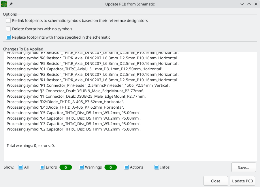
the schematic editor. To import the schematic design information into the board editor, including
footprints and net connections, use the Tools → Update Schematic from PCB… action
(F8). You can also use the
![]() icon in the top toolbar.
icon in the top toolbar.
| Update PCB from Schematic is the preferred way to transfer design information from the schematic to the PCB. In older versions of KiCad, the equivalent process was to export a netlist from the Schematic Editor and import it into the Board Editor. It is no longer necessary to use a netlist file. |
For more information about the Update Schematic from PCB tool, see the forward annotation section of the manual.
Starting from scratch
It is also possible to create a board with no matching schematic, although this workflow has some limitations and is not recommended for most users. To do this, you must start the PCB editor standalone (not from the KiCad project manager). Before beginning your design, it is a good idea to save the board file, which will also create a project file to store board settings. Use "Save As…" from the File menu to choose where to save your board file. A project file with the same name will be created in the same location you choose to save the board file in.
Board setup
Before beginning your board design, use the Board Setup dialog to configure the basic parameters of
the board. To open Board Setup, click the ![]() icon in the top
toolbar or choose "Board Setup…" from the File menu.
icon in the top
toolbar or choose "Board Setup…" from the File menu.
Configuring board stackup and physical parameters
There are two sections of Board Setup used to configure the stackup and layers of the board. The Board Editor Layers section is used to enable or disable technical (non-copper) layers, and give custom names to layers if desired. The Physical Stackup section is used to configure the number of copper layers, as well as the physical parameters of the copper and dielectric layers such as thickness and material type. Dielectric, soldermask, and silkscreen layers can have colors assigned to them, which affects the board’s appearance in the 3D viewer.
To configure the board stackup, start on the Physical Stackup section:
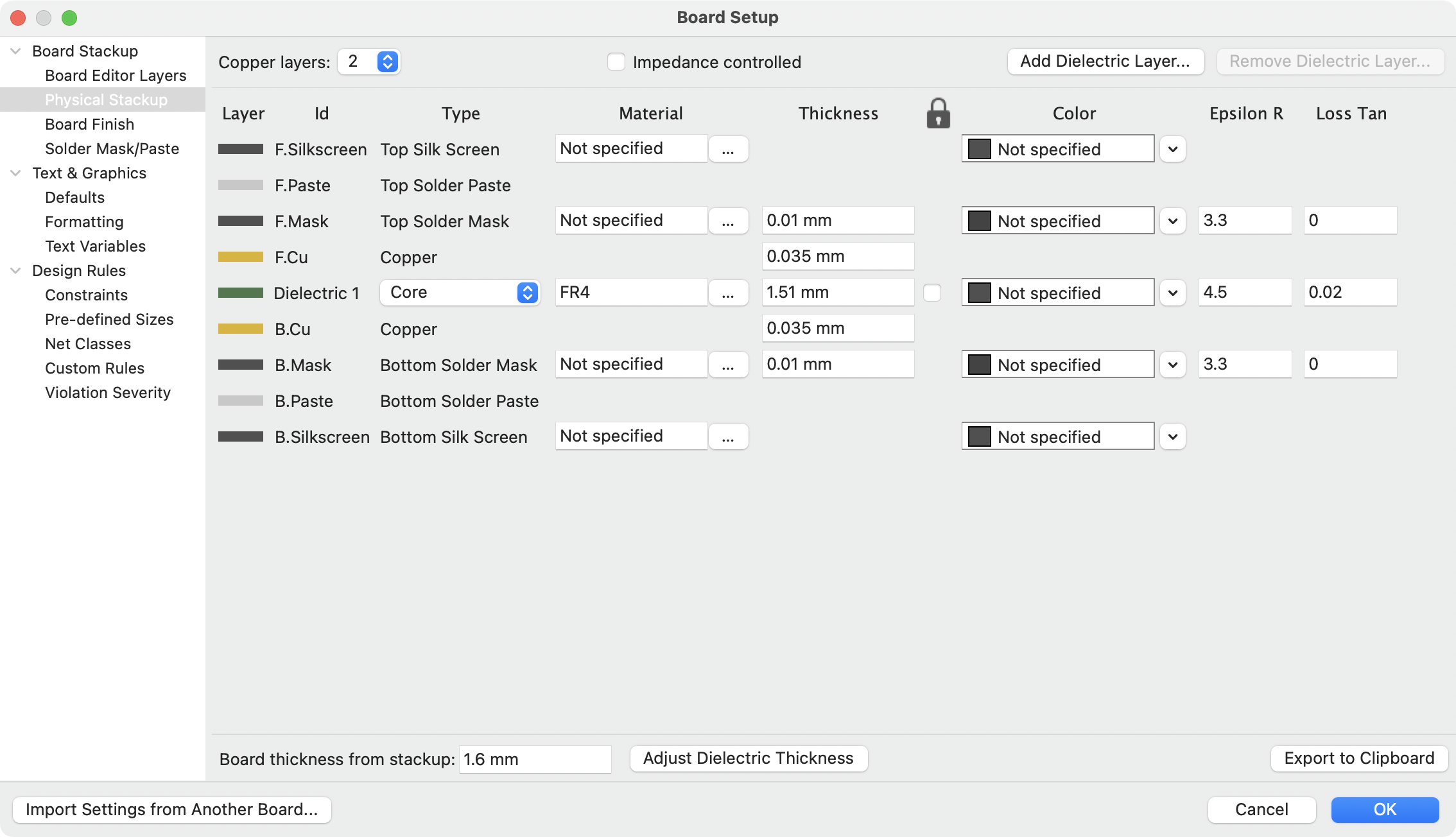
Set the number of copper layers in the upper left corner and then enter the physical parameters of the stackup if desired. These parameters may be left at their default values, but note that the board thickness value will be used when exporting a 3D model of the board. If you plan to use this feature, it is a good idea to ensure that the stackup thickness is correct.
| KiCad currently only supports stackups with an even number of copper layers. To create designs with an odd number of layers (for example, flexible printed circuits or metal-core printed circuits), simply choose the next highest even number and ignore the extra layer. |
Next, if desired, use the Board Editor Layers section to rename layers or hide non-copper layers
that you will not be using in the design. For example, if you will not use a back silkscreen on
the design, uncheck the box next to the B.Silkscreen layer.
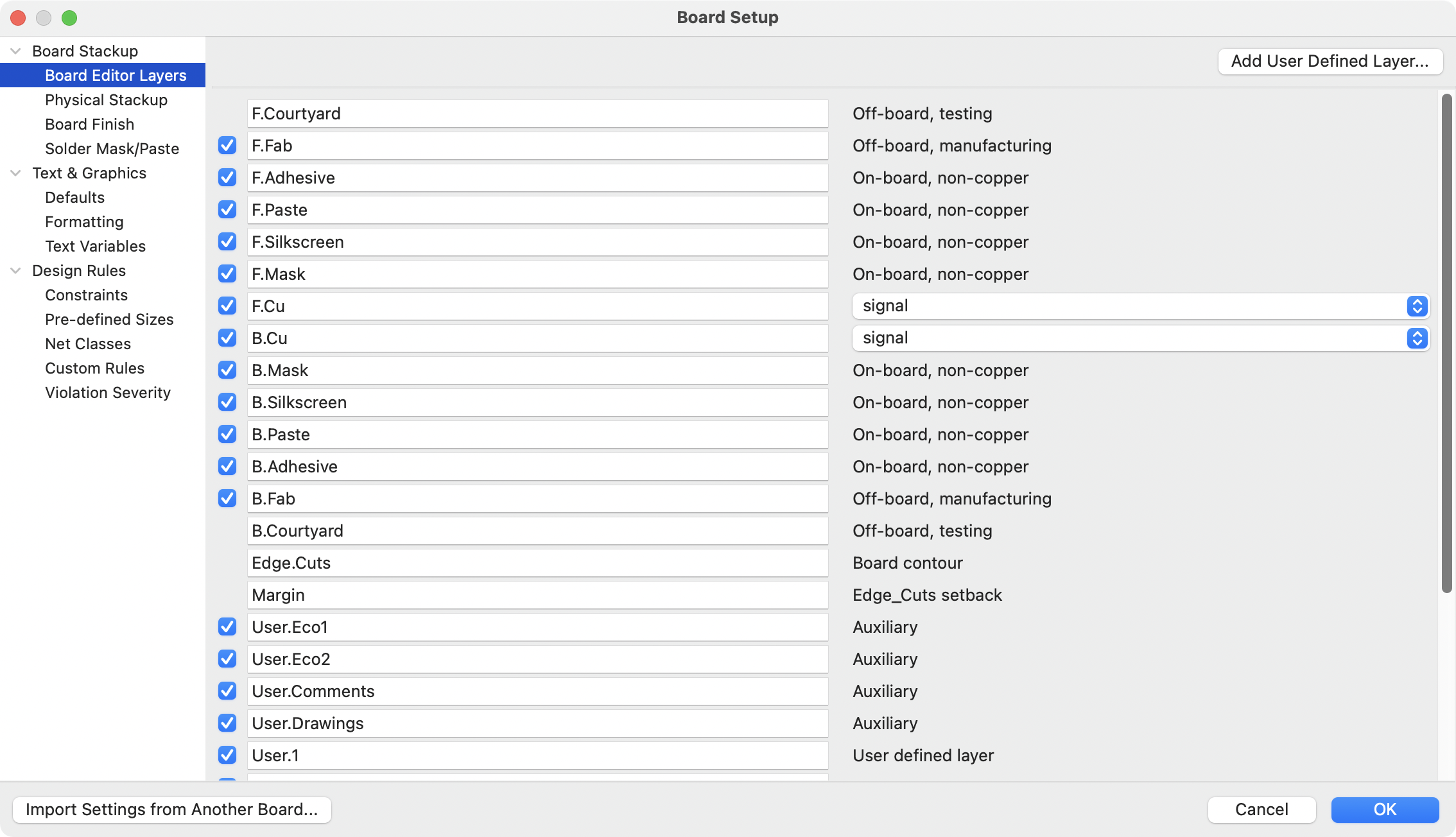
| Copper layers can be designated as signal, power plane, mixed, or jumper in the Board Editor Layers section. This designation is intended as a guide for the user only. Tracks and zones can be routed on any copper layer, no matter what the type is configured to in this dialog. |
Some additional board stackup settings are found on the Board Finish and Solder Mask/Paste sections of the Board Setup dialog. The Board Finish section has settings for defining the copper finish and special features such as castellations or edge plating. Note that these settings only impact the board attributes output as part of Gerber job files at this time.
The Solder Mask/Paste section allow global adjustment of the clearance (positive or negative) between the copper shapes and solder mask / solder paste shapes of pads on the board. These values will be added to any clearance overrides set on individual footprints or pads. Positive clearance values will result in the shape of the solder mask or paste opening being larger than the copper shape. Negative clearance values will result in the opening being smaller than the copper shape.
| Most commercial PCB fabricators expect these values to be zero and make their own adjustments to solder mask and paste openings as part of their CAM process. It is usually best to leave these values at their default of zero unless you are making the PCB yourself or have specific advice from your fabricator to use different values. |
Configuring default text and graphic settings
The Text & Graphics Defaults section of the Board Setup dialog can be used to configure the properties that will be used for new text and graphic shapes that are placed on the board.
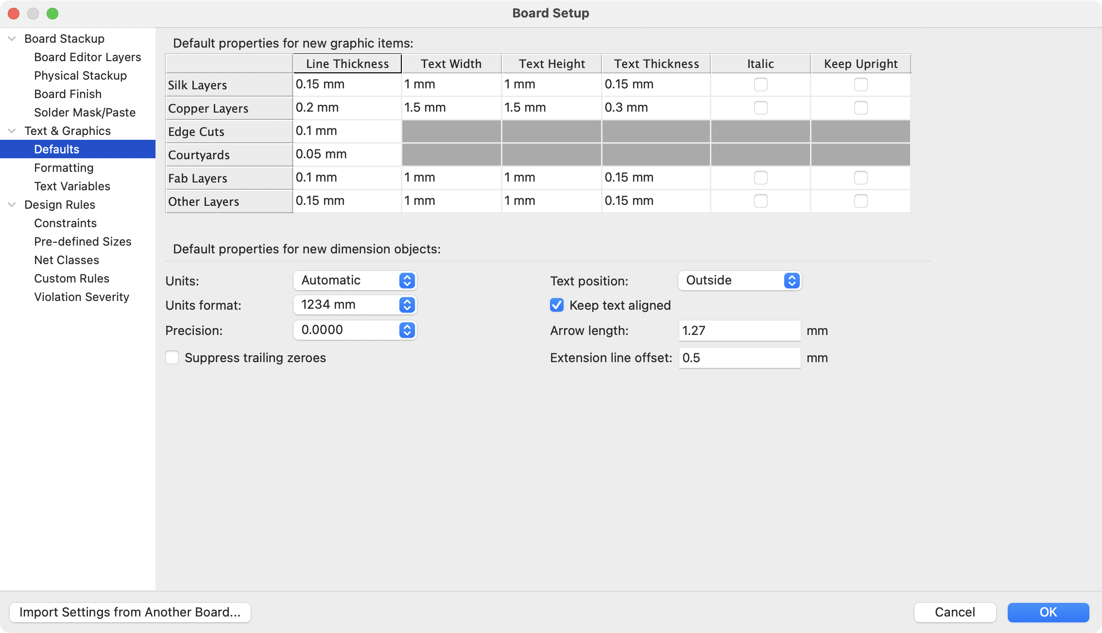
Line thickness, text size, and text appearance can be configured for the six different categories of layers shown in the dialog. Additionally, the properties for dimension objects can be configured for all layers. For more details about dimension properties, see the Dimensions section below.
Dashed line appearance is controlled in the Formatting section. Dash length
controls the length of dashes, while Gap length controls the spacing between
dashes and dots. The dash and gap lengths are relative to the line width: a gap
length of 2 means twice the width of the line.
Text replacement variables can be created in the Text Variables section. These variables allow
you to substitute the variable name for any text string. This substitution happens anywhere the
variable name is used inside the variable replacement syntax of ${VARIABLENAME}.
For example, you could create a variable named VERSION and set the text substitution to 1.0.
Now, in any text object on the PCB, you can enter ${VERSION} and KiCad will substitute 1.0. If
you change the substitution to 2.0, every text object that includes ${VERSION} will be updated
automatically. You can also mix regular text and variables. For example, you can create a text
object with the text Version: ${VERSION} which will be substituted as Version: 1.0.
Text variables can also be created in Schematic Setup. Text variables are project-wide; variables created in the schematic editor are also available in the board editor, and vice versa.
There are also a number of built-in system text variables.
Configuring design rules
Design rules control the behavior of the interactive router, the filling of copper zones, and the design rule checker. Design rules can be modified at any time, but we recommend that you establish all known design rules at the beginning of the board design process.
Constraints
Basic design rules are configured in the Constraints section of the Board Setup dialog. Constraints in this section apply to the entire board and should be set to the values recommended by your board manufacturer. Any minimum value set here is an absolute minimum and cannot be overridden with a more specific design rule. For example, if you need the copper clearance on part of a board to be 0.2mm and in the rest 0.3mm, you must enter 0.2mm for the minimum copper clearance in the Constraints section and use a netclass or custom rule to set the larger 0.3mm clearance.
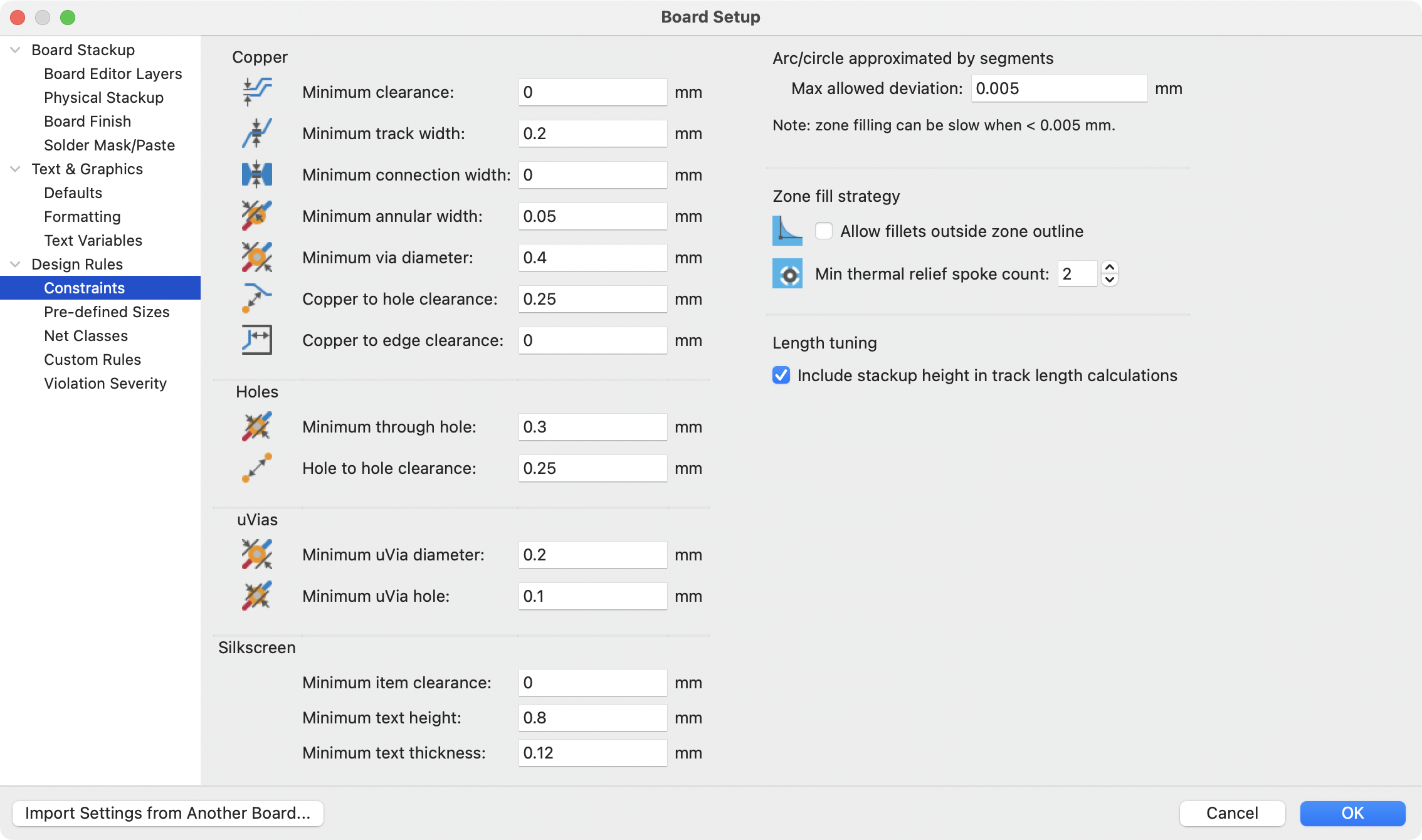
In addition to setting minimum clearances, a number of features can be configured here:
| Setting | Description |
|---|---|
Arc/circle approximated by segments |
In some situations, KiCad must use a series of straight line segments to approximate round shapes such as those of arcs and circles. This setting controls the maximum error allowed by this approximation: in other words, the maximum distance between a point on one of these line segments and the true shape of the arc or circle. Setting this to a lower number than the default value of 0.005mm will result in smoother shapes, but can be very slow on larger boards. The default value typically results in arc approximation error that is not detectable in the manufactured board due to manufacturing tolerances. |
Allow fillets outside zone outline |
Zones can have fillets (rounded corners) added in the Zone Properties dialog. By default, no zone copper, including fillets, is allowed outside the zone outline. This effectively means that inside corners of the zone outline will not be filleted even when a fillet is configured. By enabling this setting, inside corners of the zone outline will be filleted even though this results in copper from the zone extending outside the zone outline. |
Min thermal relief spoke count |
This sets the minimum acceptable number of thermal relief spokes connecting a pad to a zone. A DRC violation will be generated if this constraint is violated. |
Include stackup height in track length calculations |
By default, the height of the stackup is used to calculate the additional length of a track that travels through vias from one layer to another. This calculation relies on the board stackup height being correctly configured. In some situations, it is preferable to ignore the height of vias and just calculate the track length assuming that vias add no length. Disabling this setting will exclude via length from track length calculations. |
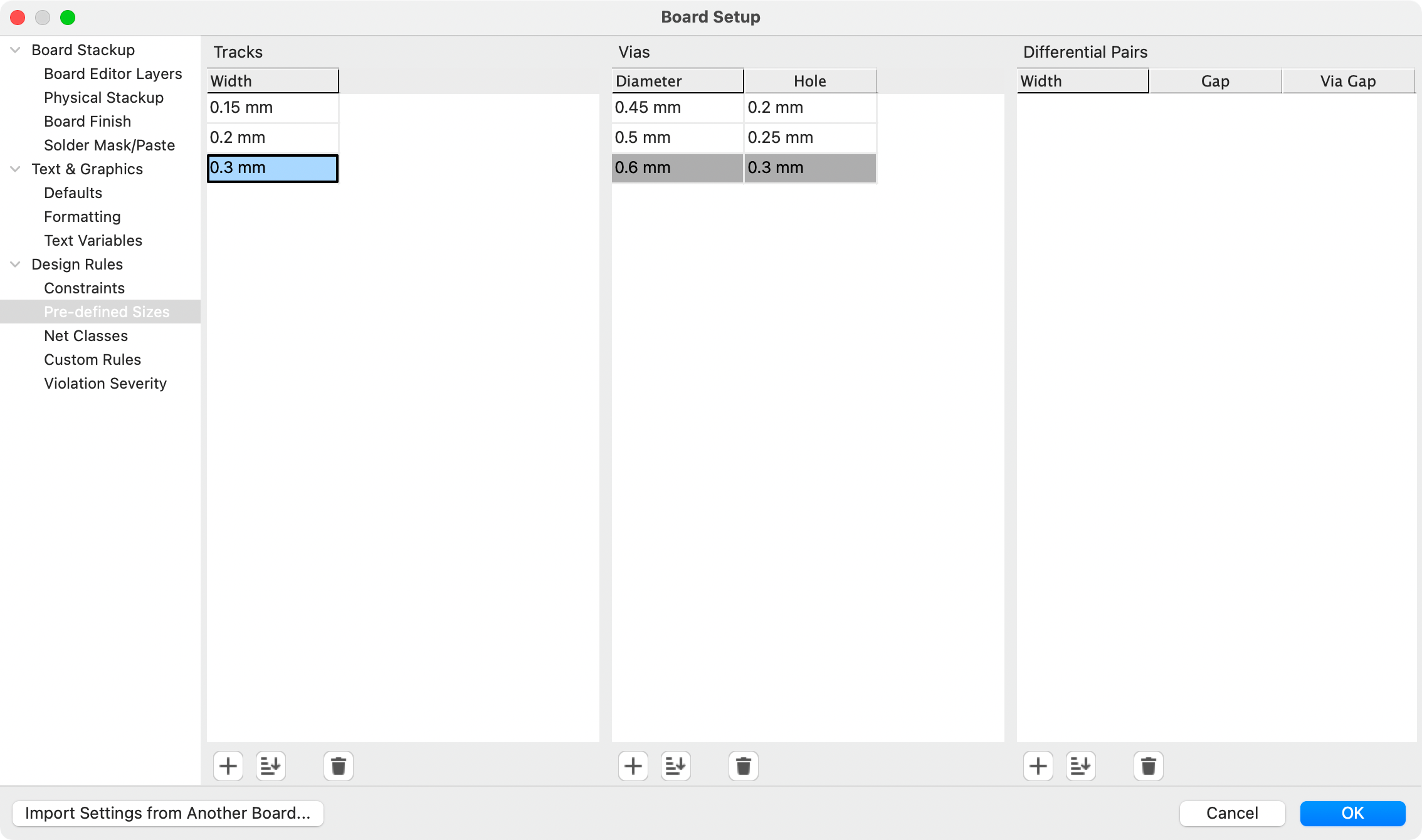
Pre-defined Sizes
The pre-defined sizes section allows you to define the track and via dimensions you want to have available while routing tracks. Net classes can be used to define the default dimensions for tracks and vias in different nets (see below) but defining a list of sizes in this section will allow you to step through these sizes while routing. For example, you may want the default track width on a board to be 0.2 mm, but use 0.3 mm for some sections that carry more current, and 0.15 mm for some sections where space is limited. You can define each of these track widths in the Board Setup dialog and then switch between them when routing traces.
Net Classes
The Net Classes section allows you to configure routing and clearance rules for different classes of nets. In KiCad, each net is part of exactly one net class. If you do not add a net to a specific class, it will be part of the Default class, which always exists. Net classes may be created and edited in either the Schematic or Board Setup dialogs.
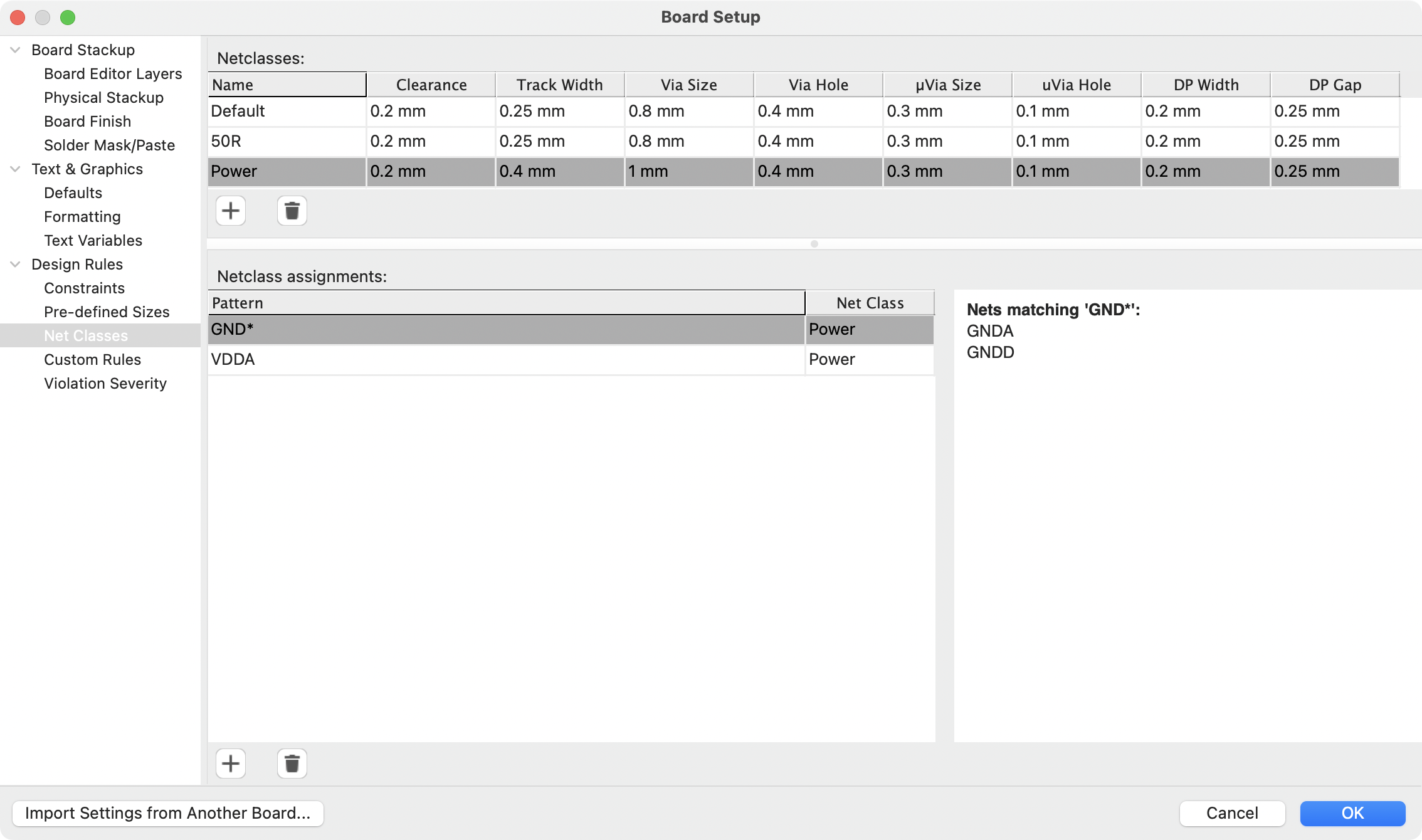
The upper portion of the Net Classes section contains a table showing the net classes in the design and the design rules that apply to each net class. Every class has values for copper clearance, track width, via sizes, and differential pair sizes. These values will be used when creating tracks and vias unless a more specific rule overrides them (see Custom Rules below).
No rule may override the minimum values set in the Constraints section of Board Setup. For
example, if you set a net class clearance to 0.1 mm, but the Minimum Clearance in the
Constraints section is set to 0.2 mm, nets in that class will have a clearance of 0.2 mm.
|
The track widths and via sizes defined for each net class are used when the track width and via size controls are set to "use netclass values" in the PCB editor. These widths and sizes are considered the default, or optimal, sizes for that netclass. They are not minimum or maximum values. Manually changing the track width or via size to a different value from that defined in the Net Classes section will not result in a DRC violation. To restrict track width or via size to specific values, use Custom Rules.
The lower portion of the Net Classes section lists pattern-based netclass assignments. Working with pattern-based netclass assignments is explained in the Schematic Editor documentation; pattern-based assignments can be edited in either the Board or Schematic Setup windows.
Note that pattern-based assignments can be created directly from the PCB editing canvas by right clicking a copper track or zone and clicking Assign netclass…. Netclasses can also be assigned in the schematic using netclass directives or labels instead of pattern-based assignments.
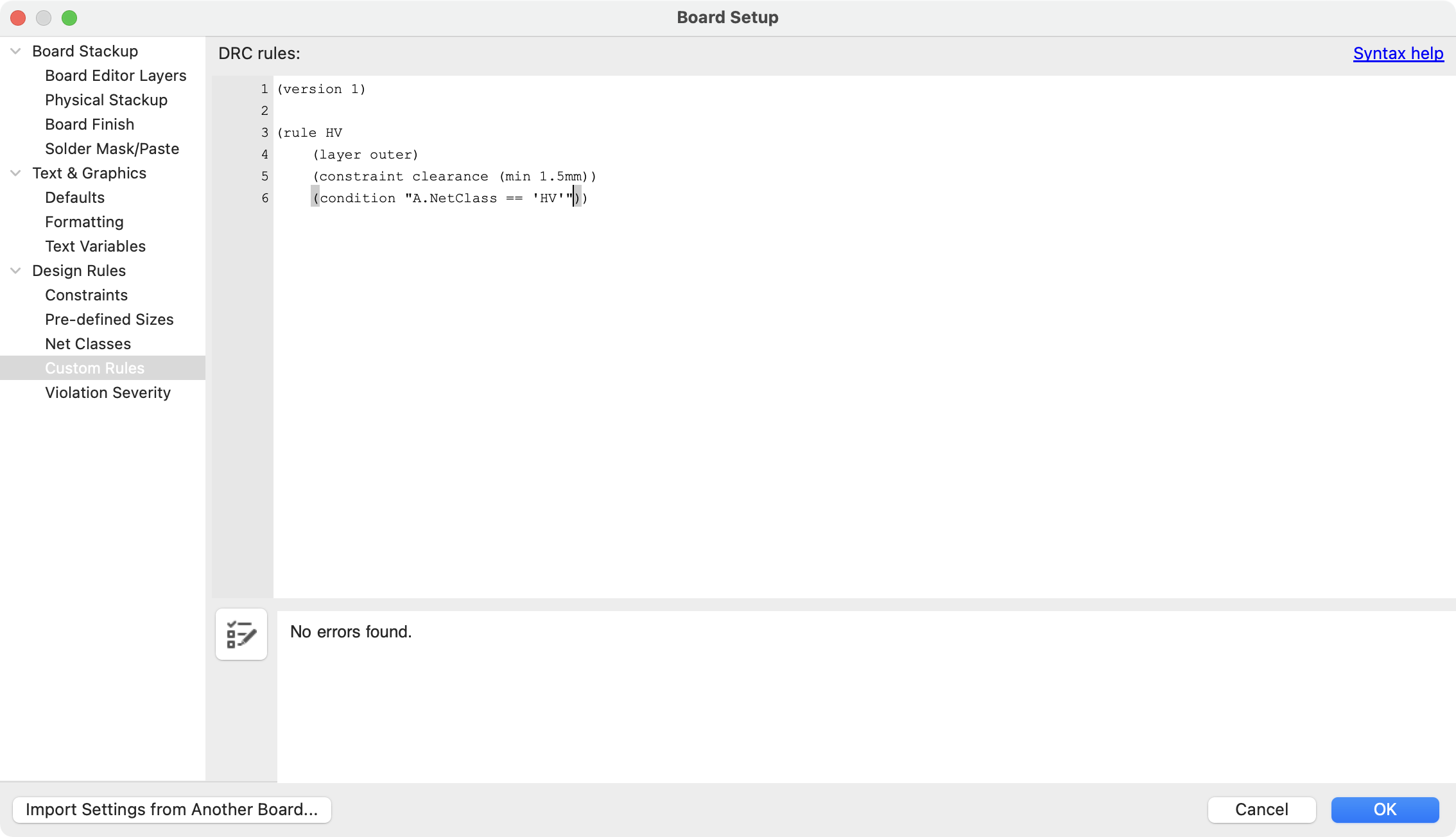
Custom Rules
The Custom Rules section contains a text editor for creating design rules using the custom rules language. Custom rules are used to create specific design rule checks that are not covered by the basic constraints or net class settings.
Custom rules will only be applied if there are no errors in the custom rules definitions. Use the Check Rule Syntax button to test the definitions and fix any problems before closing Board Setup.
See Custom Design Rules in the Advanced Topics chapter for more information on the custom rules language as well as example rules.
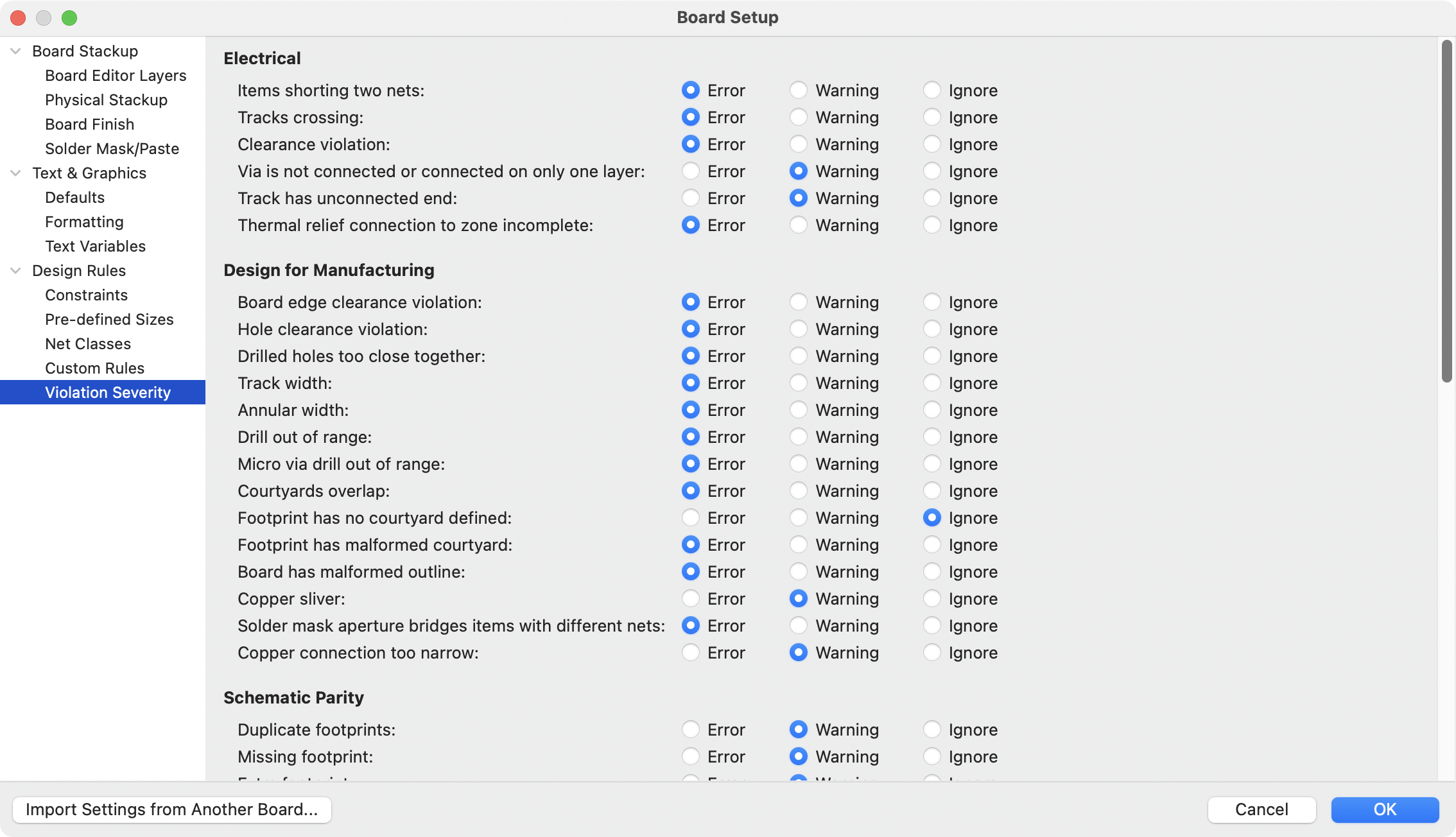
Violation Severity
The Violation Severity section allows you to configure the severity of each type of design rule check. Each rule may be set to create an error marker, a warning marker, or no marker (ignored).
| Individual rule violations may be ignored in the Design Rule Checker. Setting a rule to Ignore in the Violation Severity section will completely disable the corresponding design rule check. Use this setting with caution. |
Importing settings
You can import part or all of the board setup from an existing board. This technique can be used to create a "template" board that has the settings you want to use on multiple designs, and then importing these settings from the template board into each new board rather than entering them manually.
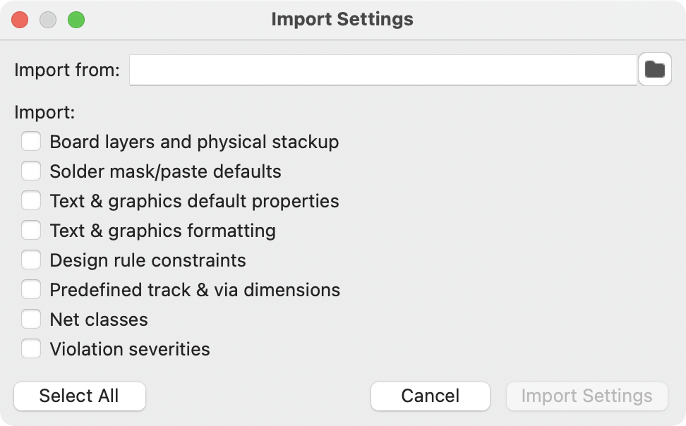
To import settings, click the Import Settings from Another Board… button at the bottom of the
Board Setup dialog and then choose the kicad_pcb file you want to import from. Select which
settings you want to import and the current settings will be overwritten with the values from the
chosen board.
Editing a board
Placement and drawing operations
Placement and drawing tools are located in the right toolbar. When a tool is activated, it stays active until a different tool is selected or the tool is canceled with the Esc key. The selection tool is always activated when any other tool is canceled.
Some toolbar buttons have more than one tool available in a palette. These tools are indicated
with a small arrow in the lower-right corner of the button:

To show the palette, you can click and hold the mouse button on the tool or click and drag the mouse. The palette will show the most recently used tool when it is closed.
|
Selection tool (the default tool). |
|
Local ratsnest tool: when the board ratsnest is hidden, selecting footprints with this tool will show the ratsnest for the selected footprint only. Selecting the same footprint again will hide its ratsnest. The local ratsnest setting for each footprint will remain in effect even after the local ratsnest tool is no longer active. |
|
Footprint placement tool: click on the board to open the footprint chooser, then click again after choosing a footprint to confirm its location. |
|
Route tracks / route differential pairs: These tools activate the interactive router and allow placing tracks and vias. The interactive router is described in more detail in the Routing Tracks section below. |
|
Tune length: These tools allow you to tune the length of single tracks or the length or skew of differential pairs, after they have been routed. See the Routing Tracks section for details. |
|
Add vias: allows placing vias without routing tracks. Vias placed on top of tracks using this tool will take on the net of the closest track segment and will become part of that track (the via net will be updated if the pads connected to the tracks are updated). Vias placed anywhere else will take on the net of a copper zone at that location, if one exists. These vias will not automatically take on a new net if the net of the copper zone is changed. |
|
Add filled zone: Click to set the start point of a zone, then configure its properties before drawing the rest of the zone outline. Zone properties are described in more detail below. |
|
Add rule area: Rule areas, formerly known as keepouts, can restrict the placement of items and the filling of zones and can also define named areas to apply specific custom design rules to. |
|
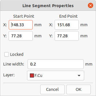
Draw lines. Note: Lines are graphical objects and are not the same as tracks placed with the Route Tracks tool. Graphical objects cannot be assigned to a net. |
|
Draw arcs: pick the center point of the arc, then the start and end points. By right clicking this button, you can change the arc editing mode between a mode that maintains the existing arc center and a mode that maintains the arc radius. |
|
Draw rectangles. Rectangles can be filled or outlines. |
|
Draw circles. Circles can be filled or outlines. |
|
Draw graphical polygons. Polygons can be filled or outlined. Note: Filled graphical polygons are not the same as filled zones: graphical polygons cannot be assigned to a net and will not keep clearance from other items. |
|
Add bitmap image. |
|
Add text. |
|
Add a textbox. |
|
Add dimensions. Dimension types are described in more detail below. |
|
Deletion tool: click objects to delete them. |
|
Set drill/place origin (used for fabrication outputs) or grid origin. |
|
Interactively measure the distance between two points. |
Snapping
When moving, dragging, and drawing board elements, the grid, pads, and other elements can have snapping points depending upon the settings in the user preferences. In complex designs, snap points can be so close together that it makes the current tool action difficult. Both grid and object snapping can be disabled while moving the mouse by using the modifier keys in the table below.
| Modifier Key | Effect |
|---|---|
Ctrl |
Disable grid snapping. |
Shift |
Disable object snapping. |
Editing object properties
All objects have properties that are editable in a dialog. Use the hotkey E or select Properties from the right-click context menu to edit the properties of selected item(s). You can only open the properties dialog if all the items you have selected are of the same type. To edit the properties of different types of items at one time, see the section below on bulk editing tools.
In properties dialogs, any field that contains a numeric value can also accept a basic math
expression that results in a numeric value. For example, a dimension may be entered as 2 * 2mm,
resulting in a value of 4mm. Basic arithmetic operators as well as parentheses for defining
order of operations are supported.
Working with footprints
Adding footprints to the board
Footprints are automatically added to the board when the PCB is updated from the schematic. The footprint associated with each schematic symbol is added to the board if it is not already present, and each footprint pad is associated with the corresponding symbol pin’s net. Symbol pins are matched to footprint pads by pin/pad number.
When footprints are added to the board after an update from the schematic, they are grouped by schematic sheet and by geographical location in the schematic. They are initially attached to the cursor; you can place them by clicking in the desired location.
You can also add footprints to the board manually using the Add Footprint tool (A or the
![]() button). Note that footprints added in this way will not be
automatically associated with a symbol or have nets assigned to their pads, and subsequent updates
from the schematic will remove these unassociated footprints unless the footprint is locked or the
Delete footprints with no symbols option is unchecked in the Update PCB From Schematic dialog.
For these reasons, it is usually recommended to avoid manually adding footprints to the board.
Manually adding footprints is necessary for PCB-only workflows, and can
also be useful for adding logos or other footprints that do not need a corresponding schematic
symbol.
button). Note that footprints added in this way will not be
automatically associated with a symbol or have nets assigned to their pads, and subsequent updates
from the schematic will remove these unassociated footprints unless the footprint is locked or the
Delete footprints with no symbols option is unchecked in the Update PCB From Schematic dialog.
For these reasons, it is usually recommended to avoid manually adding footprints to the board.
Manually adding footprints is necessary for PCB-only workflows, and can
also be useful for adding logos or other footprints that do not need a corresponding schematic
symbol.
Placing and moving footprints
Once footprints have been added to the board, you can reposition them in many ways.
The Move command (M) moves a footprint or a selection of footprints, ignoring any connected track segments that are not selected. No DRC checking is done when moving footprints with the Move command.
There is a reference point for the move operation, which is the point in the footprint which attaches to the cursor and therefore the point in the footprint that snaps to the grid and to other objects. The reference point during a move is determined by the location of the cursor when the Move command is initiated. If the cursor is over a pad, the pad’s center will be used as the reference point. If the cursor is not over a pad, the footprint’s anchor (coordinate origin point) will be used. To select an arbitrary snapping point, you can use the Move With Reference command instead of the regular Move command (right click → Positioning Tools → Move with Reference). After initiating the command, click on the desired reference point; KiCad will then begin the move with that point as the reference.
You can also use the Drag command (D) to move the selected footprint using the interactive router, maintaining all track connections to the footprint. Dragging footprints behaves like the Highlight Collisions router mode: obstacles will not be avoided or shoved, only highlighted. Only one footprint at a time can be dragged.
Flip a footprint to the opposite side of the board with the F hotkey. Any parts of the footprint on a front layer will be swapped to the corresponding back layer, and vice versa.
Rotate a footprint counter-clockwise using the R hotkey, or clockwise using Shift+R. By default, footprints are rotated by 90 degrees every time the rotate command is used, but you can configure the rotation angle step in Preferences → PCB Editor → Editing Options.
You can directly set a footprint’s exact absolute position, rotation angle, and PCB side using either the Footprint Properties dialog or the Properties panel.
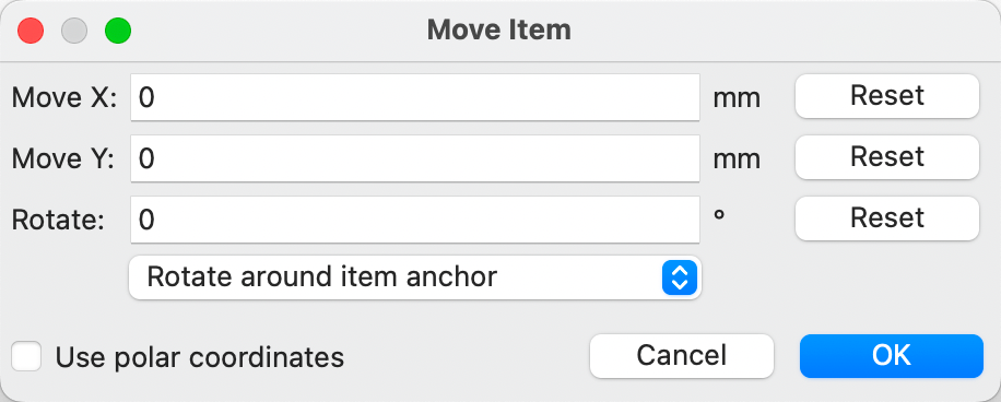
To reposition a footprint relative to its current position, use the Move Exactly tool (Shift+M). The dialog lets you specify an X and Y translation, as well as a rotation, that will be applied to the footprint. The rotation can be performed relative to either the footprint’s anchor, the local coordinate origin, or the drill/place origin. You can also use polar coordinates instead of Cartesian coordinates.
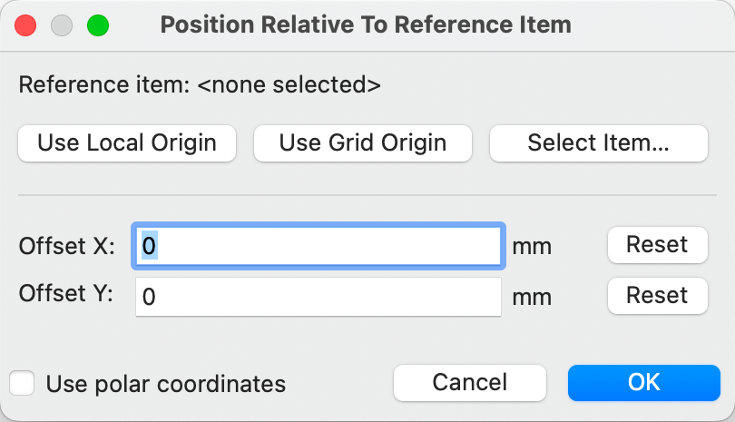
To position a footprint relative to another object, you can use the Position Relative tool (Shift+P). With this tool, you select a reference point for the move, which can be the local origin, the grid origin, or another arbitrary point, such as a pad in another footprint. The selected footprint is moved to the specified offset from the reference point.
You can swap the position of two selected footprints using the Swap command (Shift+S). The first footprint is assigned the location, rotation, and board side of the second footprint, and vice versa. If there are more than two footprints selected, the locations are cycled: the last footprint gets the position of the first footprint, the first footprint gets the location of the second, and so on.
There are several convenience features that make it easier to find, select, and move specific footprints or footprints related to another footprint.
The Get and Move Footprint command (T) prompts you to choose a footprint from a list or by typing a reference designator. KiCad then attaches the chosen footprint to your cursor for a move operation.
There are two commands to select other footprints that need to be connected to the selected footprint but don’t yet have routed connections. The Select All Unconnected Footprints command (O) selects all footprints that have ratsnest lines to the currently selected footprints. The command can be executed repeatedly to further expand the selection based on the newly selected items. The Grab Nearest Unconnected Footprint command (Shift+O) selects the closest footprint with ratsnest lines to the currently selected footprint, and additionally begins to move it. If there are multiple footprints initially selected, the command will act like the Move Individually command described below, individually moving the closest unconnected footprint for each of the initially selected footprints.
You can select footprints based on their schematic sheet using the right click → Select → Items in Same Hierarchical Sheet command, which selects all other footprints that are in the same schematic sheet as the originally selected footprint.
If you want to move multiple selected footprints in sequence, use the Move Individually command (Ctrl+M). After triggering the command, KiCad will begin moving the first selected footprint. After you click to place the footprint, KiCad will immediately start moving the next footprint, in the same order that you selected the footprints. You can skip moving a footprint by pressing Tab, commit the current move and skip any remaining moves by double-clicking, or cancel all moves (including those already completed) by pressing Esc.
If you want to move a collection of footprints at once into one area, the Pack and Move Footprints command (P) closely packs the selected footprints together and moves them as a block.
| Move Individually and Pack and Move Footprints are useful in combination with other selection convenience features, such as cross-selection from the schematic or the advanced footprint selection features described above. For example, you could select a group of bypass capacitors in the Schematic Editor, switch to the PCB Editor where the corresponding footprints are now selected, and then use Move Individually to quickly place all of the bypass capacitor footprints close to their respective ICs. Alternatively, you could use one of the other selection tools, such as Select All Unconnected Footprints, to select many footprints from all over the board, then use Pack and Move Footprints to quickly put them all into a small area. |
Finally, KiCad can automatically place footprints onto the board. The auto-place function attempts to optimally place footprints to simplify ratsnest connections to other footprints. You can auto-place the selected footprints with Place → Auto-Place Footprints → Place Selected Footprints, or auto-place all footprints outside of the board outline with Place → Auto-Place Footprints → Place Off-Board Footprints.
Footprint Properties
| This section of the KiCad documentation has not yet been written. We appreciate your patience as our small team of volunteer documentation writers work to update and expand the documentation. |
Editing Footprints
| This section of the KiCad documentation has not yet been written. We appreciate your patience as our small team of volunteer documentation writers work to update and expand the documentation. |
Working with pads
The properties of each individual pad of a footprint can be inspected and edited after placing the footprint on the board. In other words, it is possible to override the design of an individual footprint pad in a specific instance of the footprint on the board, if the footprint design in the library is not appropriate. For example, you may wish to remove the solder paste aperture for a pad that needs to remain unsoldered in a specific design, or you may wish to move the location of a through-hole pad for an axial-lead resistor in order to fit a specific design.
| By default, the position of all footprint pads are locked, so it is possible to edit the pad properties but not move the pad’s location relative to the rest of the footprint. Pads may be unlocked to allow free movement, which can be useful for certain applications (such as through-hole footprints with varying lead positions) but is generally never recommended for surface-mount footprints. |
The pad properties dialog is opened through the context menu or default hotkey E when a pad is selected. Note that KiCad assumes that if you click near a pad, you are probably trying to select the entire footprint rather than a single pad. To select a single pad, make sure to click inside the pad area, or turn off the Footprints setting in the selection filter (and make sure the Pads setting is turned on) to prevent accidental selection of the entire footprint rather than a specific pad.
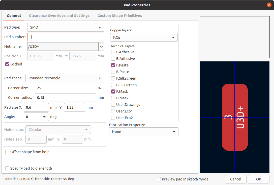
The General tab of the pad properties dialog shows the physical properties of the pad, including its geometry, shape, and layer settings.
Pad type: this setting controls which features are enabled for the pad:
SMD pads are electrically-connected and have no hole. In other words, they exist on a single copper layer.
Through-hole pads are electrically-connected and have a plated hole. The hole exists on every layer, and the copper pad exists on multiple layers (see Copper layers setting below).
Edge Connector pads are SMD pads that are allowed to overlap the board outline on the Edge.Cuts layer.
NPTH, Mechanical pads are non-plated through holes that do not have an electrical connection.
SMD Aperture pads are pads that have no hole and no electrical connection. These can be used to add specific designs to a technical layer, for example a paste or solder mask aperture.
The Copper layers setting controls which copper layers will have a shape associated with the pad.
For SMD pads, the options are F.Cu or B.Cu, controlling whether the pad sits on the front or the back of the board relative to the footprint’s location. In other words, if a pad is set to exist on B.Cu in its properties, and the footprint is flipped to the back of the board, that pad will now exist on F.Cu, because it also has been flipped.
For through-hole pads, it is possible to remove the pad shape from copper layers where the pad is not electrically connected to other copper (tracks or filled zones). Setting the copper layers to connected layers only will remove the pad shape from any unconnected layers, and setting to F.Cu, B.Cu, and connected layers will remove the pad shape from any internal unconnected layers. This can be useful in dense board designs to increase the routable area on internal layers.
The Technical layers checkboxes control which technical layers will have an aperture added with the pad’s shape. By default, pads have apertures on the paste and mask layers matching their copper layer.
| It is not possible to define a different pad shape or size on different copper layers in the current version of KiCad. |
Specify pad to die length: This setting allows a length to be associated with this pad that will be added to the routed track length by the track length tuning tools and the Net Inspector. This can be used to specify internal bondwire lengths for more accurate length matching, or in other situations where the electrical length of a net is longer than the length of the routed tracks on the board.
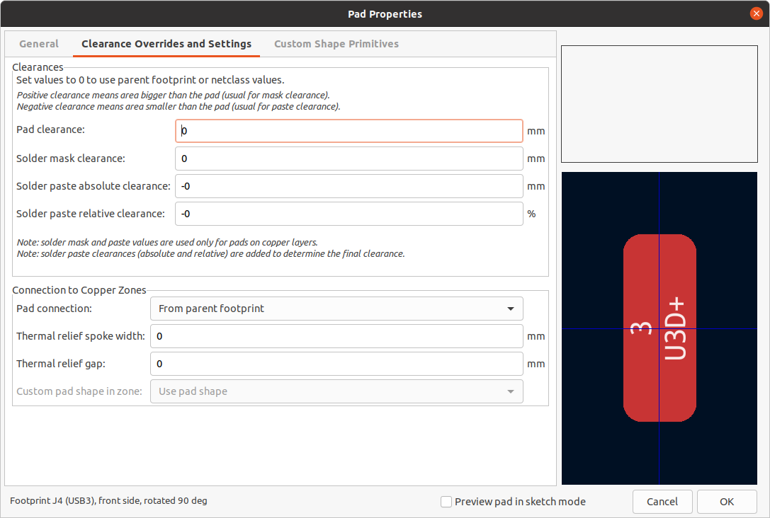
The aperture appearing on any technical layer will have the same shape and size as the pad shape on the copper layer(s). In the PCB manufacturing process, the manufacturer will often change the relative size of mask and paste apertures relative to the copper pad size, but since this size change is specific to a manufacturing process, most manufacturers expect the design data to be provided with the apertures set to the same size as the copper pads. For specific situations where you need to oversize or undersize a technical layer aperture in the design data, you can use the settings in the Overrides tab.
Pad clearance controls the minimum clearance between the pad and any copper shape (tracks,
vias, pads, zones) on a different net. This value is normally set to 0 which will cause the pad
clearance to be inherited from any clearance override set on the footprint, or the board’s design
rules and netclass rules if the footprint clearance is also set to 0.
Solder mask clearance controls the size difference between the pad shape and the aperture shape
on the F.Mask and B.Mask layers. A positive number means the solder mask aperture will be larger
than the copper shape. This number is an inflation applied to all directions. For example, a
value of 0.1mm here will cause the solder mask aperture to be inflated by 0.1mm, meaning that
there will be an 0.1mm border on all sides of the pad and the solder mask opening will be 0.2mm
wider than the pad when measured along a given axis.
Solder paste absolute clearance controls the size difference between the pad shape and the aperture shape on the F.Paste and B.Paste layers. Its behavior is otherwise identical to the behavior of the solder mask clearance setting.
Solder paste relative clearance allows setting a solder paste clearance value as a percentage of the pad size rather than an absolute distance value. If both relative and absolute clearances are specified, they are added together to determine the solder paste aperture size.
The Overrides tab also has controls for how the pad connects to any copper zone that overlaps it and shares its net.
Pad connection controls whether the pad will have a solid, thermal relief, or no connection to the zone. Like the other overrides, this one may be set for an individual pad or for an entire footprint. The default setting for this control is From parent footprint, and the default footprint setting is to use the connection mode specified in the zone properties.
Thermal relief spoke width controls the width of the spokes generated when the zone connection mode is Thermal Relief.
Thermal relief gap controls the length of the thermal spokes, or the gap between the pad’s shape and the filled copper area of the zone.
Custom pad shape in zone controls the behavior of the zone filler when the pad uses a custom shape rather than one of the default shapes. This can be used to achieve different results when using thermal reliefs and custom pad shapes.
Working with zones
Copper zones, also sometimes called copper pours or fills by other EDA tools, are solid or hatched areas of copper assigned to a particular net that automatically keep clearance from other copper objects. Zones are commonly used to fill in all free space on a board layer (or a portion of a layer) in order to create ground and power planes, carry high currents, or to provide shielding.
| Some EDA tools have separate tools for creating "plane layers" and for creating copper zones on signal layers. In KiCad, the Copper Zone tool is used for both these applications. |
Zones are defined by a polygonal outline that defines the maximum extent of the filled copper area. This outline does not represent physical copper and will not appear in exported manufacturing data. The actual copper areas of the zone must be filled each time the outline, or any objects inside the outline, are modified. The filling process may be run on a single zone, or on all zones in a board (default hotkey B). Zones may be unfilled (default hotkey Ctrl+B) to improve performance and reduce visual clutter while editing large boards.
| By default, zone filling is a manual process rather than occurring every time an object changes that would result in a change to the zone copper. This is because zone filling can be a slow process on older computers or very large designs. It is important to make sure zone fills are up-to-date before generating outputs. KiCad will check that zones have been updated and warn you before generating outputs or running DRC when zones have not yet been refilled. You can optionally enable automatic zone-filling in the Preferences dialog (PCB Editor → Editing Options → Miscellaneous → Auto-refill zones). |
To draw a zone, click the Add Filled Zone tool (![]() ) on the right
toolbar, or use default hotkey Ctrl+Shift+Z. Click to choose the first point of the zone
outline. The Zone Properties dialog will appear, allowing you to choose the zone net and other
properties. These properties may be edited at any time, so it is not critical to choose them all
correctly at first. Accept the dialog and continue placing points to define the zone outline. To
finish the zone, double-click to set the last point. Zone outline points may be modified like
graphic polygons, by dragging the square handles to move a corner or dragging the circular handles
to move an edge. To edit the zone’s properties, use hotkey E or select Properties from the
context menu.
) on the right
toolbar, or use default hotkey Ctrl+Shift+Z. Click to choose the first point of the zone
outline. The Zone Properties dialog will appear, allowing you to choose the zone net and other
properties. These properties may be edited at any time, so it is not critical to choose them all
correctly at first. Accept the dialog and continue placing points to define the zone outline. To
finish the zone, double-click to set the last point. Zone outline points may be modified like
graphic polygons, by dragging the square handles to move a corner or dragging the circular handles
to move an edge. To edit the zone’s properties, use hotkey E or select Properties from the
context menu.
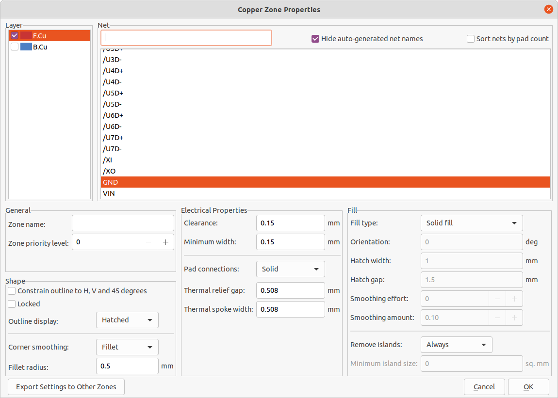
Layer: A single zone object can create filled copper on one or more copper layers. Check the box next to each copper layer that this zone outline should fill on. The copper on each layer will be filled independently, but all layers will share the same net.
Net: Select the electrical net that the zone copper should be connected to. It is possible to create zones with no net assignment. Zones with no net will keep clearance from any copper objects on any net.
Zone name can be used to assign a specific name to a zone. This name can be used to refer to the zone in custom DRC rules.
Zone priority level determines the order in which multiple zones on a single layer are filled. The highest priority level zone on a given layer will be filled first. Lower-priority zones will keep clearance to the filled areas of higher-priority zones. Two zones on the same layer with the same priority level will overlap (short-circuit) with each other, unless they are assigned different nets. When two zone outlines with the same priority and different nets touch, one zone will maintain clearance to the other so that they don’t short.
Constrain outline to H, V and 45 degrees controls the initial behavior of the zone outline drawing tool. When this option is enabled, the zone outline will be restricted to 45-degree angles. Note that after the zone outline has been created, this option has no effect. Outline points may be modified freely after creation.
Locked controls whether or not the zone outline object is locked. Locked objects may not be manipulated or moved, and cannot be selected unless the Locked Items option is enabled in the Selection Filter panel.
Outline display controls how the zone outline is drawn on screen. In Line mode, only the border lines of the outline are drawn. In Hatched mode, hatch lines are drawn on the inside of the outline border for a short distance, to make the zone outline more apparent. In Fully Hatched mode, hatch lines are drawn across the entire inside of the zone outline.
Corner smoothing controls the behavior of the filled copper areas at corners of the outline. Corners can be smoothed by a chamfer or fillet, or can extend all the way to the outline corner if smoothing is disabled.
| By default, chamfers and fillets are not added to inside corners of the zone outline, because this would result in filled copper extending outside the outline. If smooth inside corners are desired, enable the Allow fillets outside zone outline option in the Constraints section of the Board Setup dialog. |
Clearance controls the minimum clearance the filled areas of this zone will keep from other copper objects. Note that if two clearance values are in conflict, the larger clearance value will be used. For example, if a zone is set to use 0.2mm clearance but its netclass is set to use 0.3mm clearance, the result will be an 0.3mm clearance.
Minimum width controls the minimum size of narrow necks of copper created inside the zone. Any copper areas that would be below this minimum width are removed during the filling process.
Pad connection controls the way that the filled zone areas will connect to footprint pads on the same net. Solid connections will result in the copper completely overlapping the pads. Thermal reliefs will result in small copper spokes connecting the pad to the rest of the copper zone, increasing the thermal resistance between the pad and the rest of the zone. This can be useful for hand soldering. Reliefs for PTH will apply thermal reliefs to plated through-hole pads and use solid connections for surface mount pads. None will result in the zone not connecting to any pads on the same net.
Thermal relief gap controls the distance maintained between any pad and the copper zone when the pad connection mode is set to generate thermal reliefs.
Thermal spoke width controls the width of the "spokes", or short copper segments connecting the pad to the rest of the copper zone.
Fill type controls how the copper zone is filled: the default is solid fill, which will result in copper filling in all available space within the zone outline. The zone can also be set to fill a hatch pattern, which will fill the area with a pattern that contains less copper. This can be useful for flexible printed circuits and other specialty applications.
Orientation controls the angle of the hatch pattern lines. An orientation of 0 degrees will result in the hatch pattern using horizontal and vertical lines.
Hatch width controls the width of each line in the hatch pattern.
Hatch gap controls the distance between each line in the hatch pattern.
Smoothing effort controls the style of smoothing applied to the hatch pattern. A value of 0 will result in no smoothing, and a value of 3 will result in the finest smoothing. Higher values will result in longer processing time and larger Gerber files.
Smoothing amount is a ratio that controls the size of the smoothing chamfers or fillets that are generated when smoothing effort is set to a value other than 0. An amount of 0.0 results in no smoothing, and a value of 1.0 results in maximum smoothing (in other words, a chamfer or fillet equal to half of the hatch gap).
Remove islands controls the behavior of isolated copper areas, also called islands, after the initial zone fill. When this is set to always, isolated areas inside the zone are removed. When set to never, isolated areas are left alone, and will result in copper areas that are not connected to the rest of the net. When set to below area limit, a minimum island size can be specified, and islands below this threshold will be removed.
| Regardless of the remove islands setting, islands are never removed from zones that are electrically unconnected. In other words, islands are only removed from zones that have at least one electrical connection. |
Graphical objects
Graphical objects (lines, arcs, rectangles, circles, polygons, and text) can exist on any layer but
cannot be assigned to a net. Rectangles, circles, and polygons can be set to be filled or outlines
in their properties dialogs. The line width property will control the width of the outline even
for filled shapes. Line width can be set to 0 for filled shapes to disable the outline.
Creating graphical shapes
The right toolbar can be used to create lines (![]() , default hotkey
Ctrl+Shift+L), arcs (
, default hotkey
Ctrl+Shift+L), arcs (![]() , default hotkey Ctrl+Shift+A),
rectangles (
, default hotkey Ctrl+Shift+A),
rectangles (![]() ), circles (
), circles (![]() ,
default hotkey Ctrl+Shift+C), and polygons
(
,
default hotkey Ctrl+Shift+C), and polygons
(![]() , default hotkey Ctrl+Shift+P).
, default hotkey Ctrl+Shift+P).
Rectangles, circles, and polygons can be filled shapes or outlines. The line width option controls the width of the outline. The outline width extends on both sides of the "ideal" shape of the graphic object. For example, a graphic circle that is defined to have 2mm radius and 0.2mm line width will consist of a torus with an outer radius of 2.2mm and inner radius of 1.8mm. If the filled shape option is enabled and the line width is set to 0, the shape will be a filled circle with 2mm radius.
Arcs have two editing modes, which are selectable in Preferences →
PCB Editor → Editing Options or by right clicking the
![]() button on the right toolbar. The first mode
(keep arc center, adjust radius) maintains the position of the arc center as
as the arc endpoints or midpoint are dragged, changing the radius as necessary.
The second mode (keep arc endpoints or direction of starting point)
maintains the position of the arc endpoints and the arc’s direction of curvature
as the midpoint or center are dragged.
button on the right toolbar. The first mode
(keep arc center, adjust radius) maintains the position of the arc center as
as the arc endpoints or midpoint are dragged, changing the radius as necessary.
The second mode (keep arc endpoints or direction of starting point)
maintains the position of the arc endpoints and the arc’s direction of curvature
as the midpoint or center are dragged.
Creating text objects
Graphical text may be placed by using the (![]() ) icon in the right
toolbar or by keyboard shortcut Ctrl+Shift+T. Click to place the text origin, and then
edit the text and its properties in the dialog that will appear:
) icon in the right
toolbar or by keyboard shortcut Ctrl+Shift+T. Click to place the text origin, and then
edit the text and its properties in the dialog that will appear:
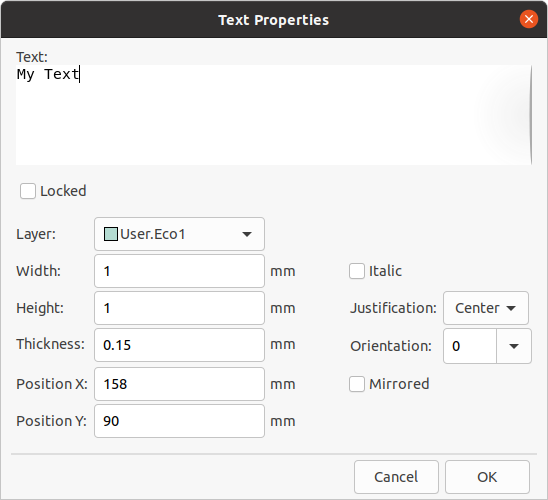
Text may be placed on any layer, but note that text on copper layers cannot be associated with a net and cannot form connections to tracks or pads. Copper zones will fill around the rectangular bounding box of text objects.
Text supports markup for superscripts, subscripts, overbars, evaluating project variables, and accessing symbol field values.
| Feature | Markup Syntax | Result |
|---|---|---|
Superscript |
|
textsuperscript |
Subscript |
|
textsubscript |
Overbar |
|
text |
|
variable_value |
|
|
field_value of symbol refdes |
| Variables must be defined in Board Setup before they can be used. There are also a number of built-in text variables. |
Board outlines (Edge Cuts)
KiCad uses graphical objects on the Edge.Cuts layer to define the board outline. The outline
must be a continuous (closed) shape, but can be made up of different types of graphical object such
as lines and arcs, or be a single object such as a rectangle or polygon. If no board outline is
defined, or the board outline is invalid, some functions such as the 3D viewer and some design rule
checks will not be functional.
Bulk editing text and graphics
Properties of text and graphics can be edited in bulk using the Edit Text and Graphic Properties dialog (Tools → Edit Text and Graphic Properties…).
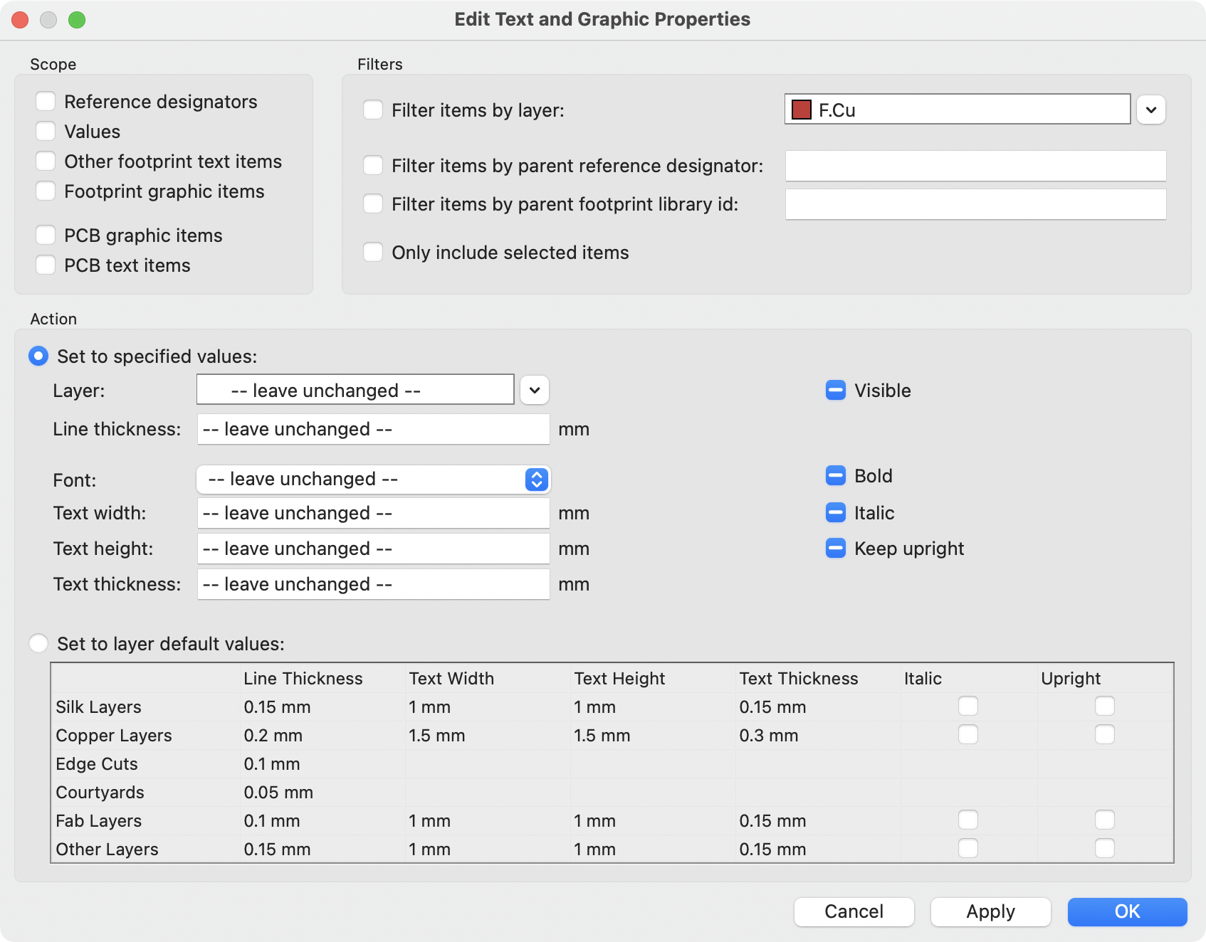
Scope and Filters
Scope settings restrict the tool to editing only certain types of objects. If no scopes are selected, nothing will be edited.
Filters restrict the tool to editing particular objects in the selected scope.
Objects will only be modified if they match all enabled and relevant filters
(some filters do not apply to certain types of objects. For example, parent
footprint filters do not apply to graphic items and are ignored for the purpose
of changing graphic properties). If no filters are enabled, all objects in the
selected scope will be modified. For filters with a text box, wildcards are
supported: * matches any characters, and ? matches any single character.
Filter items by layer filters to items on the specified board layer.
Filter other symbol fields by name filters to the specified symbol field.
Filter items by parent reference designator filters to fields in the footprint with the specified reference designator. Filter items by parent footprint library id filters to fields in footprint with the specified library identifier.
Only include selected items filters to the current selection.
Action
Properties for filtered objects can be set to new values in the bottom part of the dialog. Properties can be set to arbitrary values by selecting set to specified values or reset to their layer’s default value by selecting set to layer default values.
Drop-down lists and text boxes can be set to -- leave unchanged -- to preserve
existing values. Checkboxes can be checked or unchecked to enable or disable a
change, but can also be toggled to a third "leave unchanged" state.
All items can have their layer set.
Graphic items can have their line thickness modified.
Text properties that can be modified are font, text width, text height, text thickness (KiCad font only), emphasis (bold and italic), and orientation (keep upright). Footprint text can also have its visibility set.
Dimensions
Dimensions are graphical objects used to show a measurement or other marking on a board design. They may be added on any drawing layer, but are normally added to one of the User layers. KiCad currently supports five different types of dimension: aligned, orthogonal, center, radial, and leader.
Aligned dimensions (![]() ) show a measurement of
distance between two points. The measurement axis is the line that connects those two points, and
the dimension graphics are kept parallel to that axis.
) show a measurement of
distance between two points. The measurement axis is the line that connects those two points, and
the dimension graphics are kept parallel to that axis.
Orthogonal dimensions (![]() ) also measure the
distance between two points, but the measurement axis is either the X or Y axis. In other words,
these dimensions show the horizontal or vertical component of the distance between two points.
When creating orthogonal dimensions, you can select which axis to use as the measurement axis based
on where you place the dimension after selecting the two points to measure.
) also measure the
distance between two points, but the measurement axis is either the X or Y axis. In other words,
these dimensions show the horizontal or vertical component of the distance between two points.
When creating orthogonal dimensions, you can select which axis to use as the measurement axis based
on where you place the dimension after selecting the two points to measure.
Center dimensions (![]() ) create a cross mark to
indicate a point or the center of a circle or arc.
) create a cross mark to
indicate a point or the center of a circle or arc.
Radial dimensions (![]() ) show a measurement between
a center point and the outside of a circle or arc. The center point is indicated by a cross.
) show a measurement between
a center point and the outside of a circle or arc. The center point is indicated by a cross.
Leader dimensions (![]() ) create an arrow with a leader line
connected to a text field. This text field can contain any text, and an optional circular or
rectangular frame around the text. This type of dimension is often used to call attention to parts
of the design for reference in fabrication notes.
) create an arrow with a leader line
connected to a text field. This text field can contain any text, and an optional circular or
rectangular frame around the text. This type of dimension is often used to call attention to parts
of the design for reference in fabrication notes.
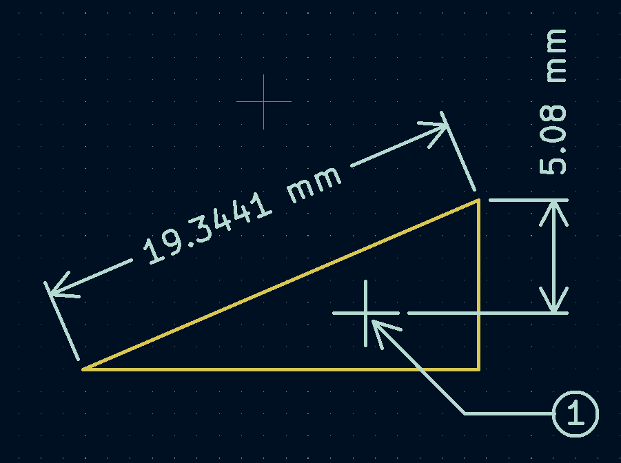
After creating a dimension, its properties may be edited (hotkey E) to change the format of the displayed number and the style of the text and graphic lines.
| You may customize the default style of newly-created dimension objects in the Text & Graphics Defaults section of the Board Setup dialog. |
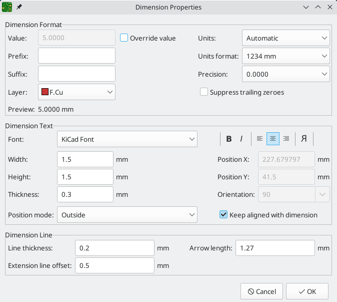
Dimension format options
Override value: When enabled, you may enter a measurement value directly into the Value field that will be used instead of the actual measured value.
Prefix: Any text entered here will be shown before the measurement value.
Suffix: Any text entered here will be shown after the measurement value.
Layer: Selects which layer the dimension object exists on.
Units: Selects which units to display the measured value in. Automatic units will result in the dimension units changing when the display units of the board editor are changed.
Units format: Select from several built-in styles of unit display.
Precision: Select how many digits of precision to display.
Dimension text options
Most of the dimension text options are identical to those options available for other graphical text objects (see the Graphical Objects section above). Some specific options for dimension text are also available:
Position mode: Choose whether to position the dimension text manually, or to automatically keep it aligned with the dimension measurement lines.
Keep aligned with dimension: When enabled, the orientation of the dimension text will be adjusted automatically to keep the text parallel with the measurement axis.
Dimension line options
Line thickness: Sets the thickness of the graphical lines that make up a dimension’s shape.
Extension line offset: Sets the distance from the measurement point to the start of the extension lines.
Arrow length: Sets the length of the arrow segments of the dimension’s shape.
Leader options
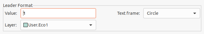
Value: Enter the text to show at the end of the leader line.
Text frame: Select the desired border around the text (circle, rectangle, or none).
Routing tracks
KiCad features an interactive router that:
-
Allows manual or guided (semi-automatic) routing of single tracks and differential pairs
-
Enables modifications of existing designs by:
-
Re-routing existing tracks when they are dragged
-
Re-routing tracks attached to footprint pads when the footprint is dragged
-
-
Allows tuning of track lengths and differential pair skew (phase) by inserting serpentine
tuning shapes for designs with tight timing requirements
By default, the router respects the configured design rules when placing tracks: the size (width) of new tracks will be taken from the design rules and the router will respect the copper clearance set in the design rules when determining where new tracks and vias can be placed. It is possible to disable this behavior if desired by using the Highlight Collisions router mode and turning on the Allow DRC Violations option in the router settings (see below).
The router has three modes that can be selected at any time. The router mode is used for routing new tracks, but also when dragging existing tracks using the Drag (hotkey D) command. These modes are:
-
Highlight Collisions: in this mode, most of the router features are disabled and routing is fully manual. When routing, collisions (clearance violations) will be highlighted in green and the newly-routed tracks cannot be fixed in place if there is a collision unless the Allow DRC Violations option is turned on. In this mode, up to two track segments may be placed at a time (for example, one horizontal and one diagonal segment).
-
Shove: in this mode, the track being routed will walk around obstacles that cannot be moved (for example, pads and locked tracks/vias) and shove obstacles that can be moved out of the way. The router prevents DRC violations in this mode: if there is no way to route to the cursor position that does not violate DRC, no new tracks will be created.
-
Walk Around: in this mode, the router behaves the same as in Shove mode, except no obstacles will be moved out of the way.
Which mode to use is a matter of preference. For most users, we recommend using Shove mode for the most efficient routing experience or Walk Around mode if you do not want the router to modify tracks that are not being routed. Note that Shove and Walk Around modes always create horizontal, vertical, and 45-degree (H/V/45) track segments. If you need to route tracks with angles other than H/V/45, you must use Highlight Collisions mode and enable the Free Angle Mode option in the Interactive Router Settings dialog.
There are five main routing functions: Route Single Track, Route Differential Pair, Tune length of a single track, Tune length of a differential pair, and Tune skew of a differential pair. All of these are present in both the Route menu dropdown (individually) on the top toolbar and the drawing toolbar in two overloaded icons on the drawing toolbar on the right. The use of the overloaded icons is described above. One is for the two Route functions and one is for the three Tune functions. In addition, the Route menu allows the selection of Set Layer Pair and Interactive Router Settings.
To route tracks, click the Route Tracks ![]() icon (from the
drawing toolbar or from the top toolbar under Route) or use the hotkey X. Click on a
starting location to select which net to route and begin routing. The net being routed will
automatically be highlighted and the allowable clearance for the net will be indicated with a
gray outline around the tracks being routed. The clearance outline can be disabled by changing
the Clearance Outlines setting in the Display Options section of the Preferences dialog.
icon (from the
drawing toolbar or from the top toolbar under Route) or use the hotkey X. Click on a
starting location to select which net to route and begin routing. The net being routed will
automatically be highlighted and the allowable clearance for the net will be indicated with a
gray outline around the tracks being routed. The clearance outline can be disabled by changing
the Clearance Outlines setting in the Display Options section of the Preferences dialog.
| The clearance outline shows the maximum clearance from the routed net to any other copper on the PCB. It is possible to use custom design rules to specify different clearances for a net to different objects. These clearances will be respected by the router, but only the largest clearance value will be shown visually. |
When the router is active, new track segments will be drawn from the routing start point to the editor cursor. These tracks are unfixed temporary objects that show what tracks will be created when you use a left-click or the Enter key to fix the route. The unfixed track segments are shown in a brighter color than the fixed track segments. When you exit the router using the Esc key or by selecting another tool, only the fixed track segments will be saved. The Finish Route action (hotkey End) will fix all tracks and exit the router.
While you are routing, you can use the Undo Last Segment command (hotkey Backspace) to unfix the tracks you most recently fixed. You can use this command repeatedly to step back through the route that you have already fixed.
In previous versions of KiCad, using the left mouse button or Enter to fix the routed segments would fix all segments up to but not including the segment ending at the mouse cursor location. In KiCad 6 and later, this behavior is optional, and by default, all segments including the one ending at the mouse cursor location will be fixed. The old behavior can be restored by disabling the "Fix all segments on click" option in the Interactive Router Settings dialog.
While routing, you can hold the Ctrl key to disable grid snapping, and hold the Shift key to disable snapping to objects such as pads and vias.
| Snapping to objects can also be disabled by changing the Magnetic Points preferences in the Editing Options section of the Preferences dialog. We recommend that you leave object snapping enabled in general, so that you do not accidentally end tracks slightly off-center on a pad or via. |
Track posture
When routing in H/V/45 mode, the posture refers to how a set of two track segments connect two points that cannot be reached by a single H/V/45-degree segment. In such a case, the points will be connected by one horizontal or vertical segment and one diagonal (45-degree) segment. The posture refers to the order of these segments: whether the horizontal/vertical segment or the diagonal segment comes first.


KiCad’s router attempts to pick the best posture automatically based on a number of factors. In general, the router will attempt to minimize the number of corners in a route, and will avoid "bad" corners such as acute angles whenever possible. When routing from or to a pad, KiCad will choose the posture that lines up the route with the longest edge of the pad.
In some cases, KiCad cannot guess the posture you intend correctly. To switch the posture of the track while routing, use the Switch Track Posture command (hotkey /).
In situations where there is no obvious "best" posture (for example, when starting a route from a via), KiCad will use the movement of your mouse cursor to select the posture. If you would like the route to begin with a straight (horizontal or vertical) segment, move the mouse away from the starting location in a mostly horizontal or vertical direction. If you would like the route to begin diagonally, move in a diagonal direction. Once the cursor is a sufficient distance away from the routing start location, the posture is "locked" and will no longer change unless the cursor is brought back to the starting location. Detection of posture from the movement of the mouse cursor can be disabled in the Interactive Router Settings dialog as described below.
| If you use the Switch Track Posture command to override the posture chosen by KiCad, the automatic detection of posture from mouse movement will be disabled for the remainder of the current routing operation. |
Track corner mode
KiCad’s router can place tracks with either sharp or rounded (arc) corners when routing in H/V/45 mode. To switch between sharp and rounded corners, use the Track Corner Mode command (hotkey Ctrl+/). When routing with rounded corners, each routing step will place either a straight segment, a single arc, or both a straight segment and an arc. The track posture determines whether the arc or the straight segment will be placed first.
Track corners can also be rounded after routing by using the Fillet Tracks command after selecting the desired tracks.
| Dragging of tracks with arcs is not yet supported. Arcs will be converted back to sharp corners when dragging tracks or when tracks are moved by the router in Shove mode. |
Track width
The width of the track being routed is determined in one of three ways: if the routing start point
is the end of an existing track and the ![]() button on the top
toolbar is enabled, the width will be set to the width of the existing track. Otherwise, if the
track width dropdown in the top toolbar is set to "use netclass width", the width will be taken
from the netclass of the net being routed (or from any custom design rules that specify a different
width for the net, such as inside a neckdown area). Finally, if the track width dropdown is set to
one of the pre-defined track sizes configured in the Board Setup dialog, this width will be used.
button on the top
toolbar is enabled, the width will be set to the width of the existing track. Otherwise, if the
track width dropdown in the top toolbar is set to "use netclass width", the width will be taken
from the netclass of the net being routed (or from any custom design rules that specify a different
width for the net, such as inside a neckdown area). Finally, if the track width dropdown is set to
one of the pre-defined track sizes configured in the Board Setup dialog, this width will be used.
| The track width can never be lower than the minimum track width configured in the Constraints section of the Board Setup dialog. If a pre-defined width is added that is lower than this minimum constraint, the minimum constraint value will be used instead. |
KiCad’s router supports a single track width for the active route. In other words, to change widths in the middle of a track, you must end the route and then restart a new route from the end of the previous route. To change the width of the active route, use the hotkeys W and Shift+W to step through the track widths configured in the Board Setup dialog.
Placing vias
While routing tracks, switching layers will insert a through via at the end of the current (unfixed) track. Once you place the via, routing will continue on the new layer. There are several ways to select a new layer and insert a via:
-
By using the hotkey to select a specific layer, such as PgUp to select
F.Cuor PgDn to selectB.Cu. -
By using the "next layer" or "previous layer" hotkeys (+ and -).
-
By using the "Place Via" hotkey (V), which will switch to the next layer in the active layer pair.
-
By using the Select Layer and Place Through Via action (hotkey <), which will open a dialog to select the target layer.
After using any of the above methods to add a via and change layer, but before clicking to fix the via and commit the current trace segment, you can cancel placing the via by pressing V. The via will be removed and routing will continue on the original layer.
You can place a via and end the current trace, without changing layers, by pressing V and then double-clicking or Shift-clicking to place the via.
The size of the via will be taken from the active Via Size setting, accessible from the drop-down in the top toolbar or the Increase Via Size (') and Decrease Via Size (\) hotkeys. Much like track width, when the via size is set to "use netclass sizes", the via sizes configured in the Net Classes section of the Board Setup will be used (unless overridden by a custom design rule).
If microvias or blind/buried vias are enabled in the Constraints section of the Board Setup dialog, these vias can be placed while routing. Use the hotkey Ctrl+V to place a microvia and Alt+Shift+V to place a blind/buried via. Microvias may only be placed such that they connect one of the outer copper layers to an adjacent layer. Blind/buried vias may be placed on any layer.
Vias placed by the router are considered to be part of a routed track. This means that the via net can be updated automatically (just like track nets can), for example when updating the PCB from the schematic changes the net name of the track. In some cases this may not be desired, such as when creating stitching vias. The automatic update of via nets can be disabled for specific vias by turning off the "automatically update via nets" checkbox in the via properties dialog. Vias placed with the Add Free-standing Vias tool are created with this setting disabled.
Routing Convenience Functions
KiCad offers several functions to make certain routing operations more convenient.
If you need to route a number of traces from a set of pads, you can use the Route Selected tool to quickly route from each pad in sequence. Select the pads you want to use as starting points, then press Shift+X to route from each pad in sequence. The router will begin a trace from the first selected pad, which you can route as you would any other trace. When you complete the trace, the router will automatically begin a new trace from the next pad in the selection, in the same order that you selected the pads. Pads that already have traces attached are skipped. You can also skip routing the current trace and move on to the next pad by pressing Esc. You can also select footprints instead of pads; all unrouted pads in the selected footprints will be used as starting points.
If you want to route a number of traces to a set of pads, instead of from the pads, you can use the Route Selected From Other End tool (Shift+E). This tool works the same way as the Route Selected tool, except it uses each selected pad as an end point rather than a starting point. The starting point for each trace is the other end of the ratsnest line for each selected pad.
Routing from the other end is also possible while routing individual traces: press E while routing a trace to commit the current segment and begin routing from the other end of the in-progress trace’s ratsnest line.
Finally, you can quickly unroute traces connected to an object (footprint, pad, or trace) by selecting the object, right-clicking, and selecting Unroute Selected. Any traces connected to the selected object will be removed, starting at the selected object and continuing until another pad is encountered.
Automatically completing traces
KiCad’s router can automatically route individual traces, based on the connections defined in the schematic. This can be thought of as a limited form of auto-routing that considers a single trace at a time. The router will only use the current layer; it will not use vias or change layers.
While routing, press the F key to have the router attempt to automatically finish the current trace. The trace will be automatically routed from the end of the last fixed trace segment to the closest ratsnest anchor. If the router can’t automatically finish the trace, it will allow you to complete the trace manually. This action can also be performed by clicking Attempt Finish in the context menu while routing.
When the router is not the active tool, you can automatically route multiple traces by selecting footprints, pads, and traces to route from and pressing Shift+F. You do not need to select both ends of a desired connection; the router will route from the selected item to its nearest ratsnest anchor. If multiple items were selected, each item will be routed in sequence, in the order that they were selected. If a connection cannot be automatically completed, the tool will pause with the router active so that you can complete the trace manually. With the automatic completion paused for a manual connection, you can press Esc to skip routing the current trace. After manually completing the trace or skipping the connection, the tool will continue attempting to route the remaining connections.
Routing differential pairs
Differential pairs in KiCad are defined as nets with a common base name and a positive and
negative suffix. KiCad supports using ` and `-`, or `P` and `N` as the suffix. For example, the
nets `USB and USB- form a differential pair, as do the nets USB_P and USB_N. In the first
example, the base name is USB, and USB_ in the second. The suffix styles cannot be mixed: the
nets USB+ and USB_N do not form a differential pair. Make sure you name your differential pair
nets accordingly in the schematic in order to allow use of the differential pair router in the PCB
editor.
To route a differential pair, click the Route Differential Pairs
![]() icon (from the drawing toolbar or from the top toolbar under
Route) or use the hotkey 6. Click on a pad, via, or the end of an existing differential
pair track to start routing. You can start routing from either the positive or negative net of a
differential pair.
icon (from the drawing toolbar or from the top toolbar under
Route) or use the hotkey 6. Click on a pad, via, or the end of an existing differential
pair track to start routing. You can start routing from either the positive or negative net of a
differential pair.
| It is not currently possible to start routing a differential pair in the middle of an existing differential pair track. |
The differential pair router will attempt to route the pair of tracks with a gap taken from the design rules (differential pair gap can be configured in the Net Classes section of the Board Setup dialog, or by using custom design rules). If the starting or ending location of the route is a different distance apart from the configured gap, the router will create a short "fan out" section to minimize the length of track where the differential pair is not coupled.
When switching layers or using the Place Via (V) action, the differential pair router will create two vias next to each other. These vias will be placed as close as possible to each other while respecting the design rules for copper and hole-to-hole clearance.
Modifying tracks
After tracks have been routed, they can be modified by moving or dragging, or deleted and re-routed. When a single track segment is selected, the hotkey U can be used to expand the selection to all connected track segments. The first press of U will select track segments between the nearest junctions with pads or vias. The second press of U will expand the selection again to include all track segments connected to the selected track on all layers. Selecting tracks with this technique can be used to quickly delete an entire routed net.
There are two different drag commands that can be used to modify a track segment. The Drag (45-degree mode) command, hotkey D, is used to drag tracks using the router. If the router mode is set to Shove, dragging with this command will shove nearby tracks. If the router mode is set to Walk Around, dragging with this command will walk around or stop at obstacles. The Drag Free Angle command, hotkey G, is used to split a track segment into two and drag the new corner to any location. Drag Free Angle behaves like the Highlight Collisions router mode: obstacles will not be avoided or shoved, only highlighted.
| Dragging of tracks containing arcs is not yet possible. Attempting to drag these tracks will result in the arcs being removed in some cases. It is possible to resize a particular arc by selecting it and using the drag command (D). When resizing an arc using this command, no DRC checking is performed. |
The Move command (hotkey M) can also be used on track segments. This command will pick up the selected track segments, ignoring any attached track segments or vias that are not selected. No DRC checking is done when moving tracks using the Move command.
It is possible to re-route tracks attached to footprints while moving the footprints. To do so, use the drag command (D) with a footprint selected. Any tracks that end at one of the footprint’s pads will be dragged along with the footprint. This feature has some limitations: it only operates in Highlight Collisions mode, so the tracks attached to footprints will not walk around obstacles or shove nearby tracks out of the way. Additionally, only tracks that end at the origin of the footprint’s pads will be dragged. Tracks that simply pass through the pad or that end on the pad at a location other than the origin will not be dragged.
It is possible to modify the width of tracks and the size of vias without re-routing them using the Edit Tracks and Vias dialog. See the section below on bulk editing tools for details.
Length tuning
The length tuning tools can be used to add serpentine tuning shapes to tracks after routing. To
tune the length of a track, first pick the appropriate length tuning tool. The single track tuning
tool (icon ![]() or hotkey 7) will add serpentine shapes
to bring the length of a single track up to the target value. The differential pair tuning tool
(icon
or hotkey 7) will add serpentine shapes
to bring the length of a single track up to the target value. The differential pair tuning tool
(icon ![]() or hotkey 8) will do the same for a
differential pair. The differential pair skew tuning tool (icon
or hotkey 8) will do the same for a
differential pair. The differential pair skew tuning tool (icon
![]() or hotkey 9) will add length to the
shorter member of a differential pair in order to eliminate skew (phase difference) between the
positive and negative sides of the pair. As with the Routing icons, the Tuning icons are found
in both the Route menu dropdown from the top toolbar and the drawing toolbar on the right.
or hotkey 9) will add length to the
shorter member of a differential pair in order to eliminate skew (phase difference) between the
positive and negative sides of the pair. As with the Routing icons, the Tuning icons are found
in both the Route menu dropdown from the top toolbar and the drawing toolbar on the right.
To select the target length for the length tuning tools, open the Length Tuning Settings dialog from the context menu or with the hotkey Ctrl+L after activating the length tuning tool:
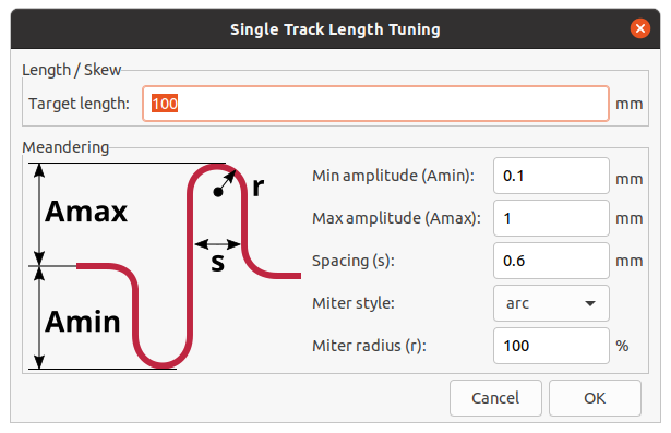
This dialog can also be used to configure the size, shape, and spacing of the meander shapes.
After configuring the target length, click a track in the area that you wish to start placing meander shapes. Move the mouse cursor along the track, and meander shapes will be added. A status window will appear next to the cursor showing the current length of the track and the target length. Click again to finish placing the current meander. Multiple meanders can be placed on the same track if desired.
| The length tuning tools only support tuning the length of point-to-point nets between two pads. Tuning the length of nets with different topologies is not yet supported. |
Interactive router settings
The interactive router settings can be accessed through the Route menu, or by right-clicking on the Route Tracks button in the toolbar. These settings control the router behavior when routing tracks as well as when dragging existing tracks.
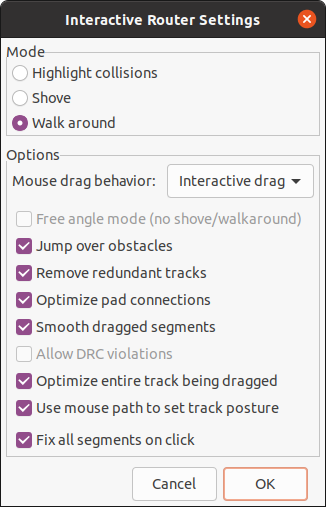
| Setting | Description |
|---|---|
Mode |
Sets the operating mode of the router for creating new tracks and dragging existing tracks. See above for more information. |
Free angle mode |
Allows routing tracks at any angle, instead of just at 45-degree increments. This option is only available if the router mode is set to Highlight collisions. |
Jump over obstacles |
In Shove mode, allows the router to attempt to move colliding tracks behind solid obstacles (such as pads). |
Remove redundant tracks |
Automatically removes loops created in the currently-routed track, keeping only the most recently routed section of the loop. |
Optimize pad connections |
When this setting is enabled, the router attempts to avoid acute angles and other undesirable routing when exiting pads and vias. |
Smooth dragged segments |
When dragging tracks, attempts to combine track segments together to minimize direction changes. |
Allow DRC violations |
In Highlight collisions mode, allows placing tracks and vias that violate DRC rules. It has no effect in other modes. |
Optimize entire track being dragged |
When enabled, dragging a track segment will result in KiCad optimizing the rest of the track that is visible on the screen. The optimization process removes unnecessary corners, avoids acute angles, and generally tries to find the shortest path for the track. When disabled, no optimizations are performed to the track outside of the immediate section being dragged. |
Use mouse path to set track posture |
Attempts to pick the track posture based on the mouse path from the routing start location. |
Fix all segments on click |
When enabled, clicking while routing will fix the position of all the track segments that have been routed, including the segment that ends at the mouse cursor. A new segment will be started from the mouse cursor location. When disabled, the last segment (the one that ends at the mouse cursor) will not be fixed in place and can be adjusted by further mouse movement. |
Forward and back annotation
Update PCB From Schematic (forward annotation)
Use the Update PCB from Schematic tool to sync design information from the
Schematic Editor to the Board Editor. The tool can be accessed with Tools →
Update PCB from Schematic (F8) in both the schematic and board
editors. You can also use the
![]() icon in the top toolbar of the Board Editor. This process is often called
forward annotation.
icon in the top toolbar of the Board Editor. This process is often called
forward annotation.
| Update PCB from Schematic is the preferred way to transfer design information from the schematic to the PCB. In older versions of KiCad, the equivalent process was to export a netlist from the Schematic Editor and import it into the Board Editor. It is no longer necessary to use a netlist file. |
The tool adds the footprint for each symbol to the board and transfers updated schematic information to the board. In particular, the board’s net connections are updated to match the schematic.
The changes that will be made to the PCB are listed in the Changes To Be Applied pane. The PCB is not modified until you click the Update PCB button.
You can show or hide different types of messages using the checkboxes at the bottom of the window. A report of the changes can be saved to a file using the Save… button.
Options
The tool has several options to control its behavior.
| Option | Description |
|---|---|
Re-link footprints to schematic symbols based on their reference designators |
Footprints are normally linked to schematic symbols via a unique identifier created when the symbol is added to the schematic. A symbol’s unique identifier cannot be changed. If checked, each footprint in the PCB will be re-linked to the symbol that has the same reference designator as the footprint. If unchecked, footprints and symbols will be linked by unique identifier as usual, rather than by reference designator. Each footprint’s reference designator will be updated to match the reference designator of its linked symbol. This option should generally be left unchecked. It is useful for specific workflows that rely on changing the links between schematic symbols and footprints, such as refactoring a schematic for easier layout or replicating layout between identical channels of a design. |
Delete footprints with no symbols |
If checked, any footprint in the PCB without a corresponding symbol in the schematic will be deleted from the PCB. Footprints with the "Not in schematic" attribute will be unaffected. If unchecked, footprints without a corresponding symbol will not be deleted. |
Replace footprints with those specified in the schematic |
If checked, footprints in the PCB will be replaced with the footprint that is specified in the corresponding schematic symbol. If unchecked, footprints that are already in the PCB will not be changed, even if the schematic symbol is updated to specify a different footprint. |
Update Schematic from PCB (back annotation)
The typical workflow in KiCad is to make changes in the schematic and then sync the changes to the board using the Update PCB From Schematic tool. However, the reverse process is also possible: design changes can be made in the board and then synced back to the schematic using Tools → Update Schematic From PCB in either the schematic or board editors. This process is often called back annotation.
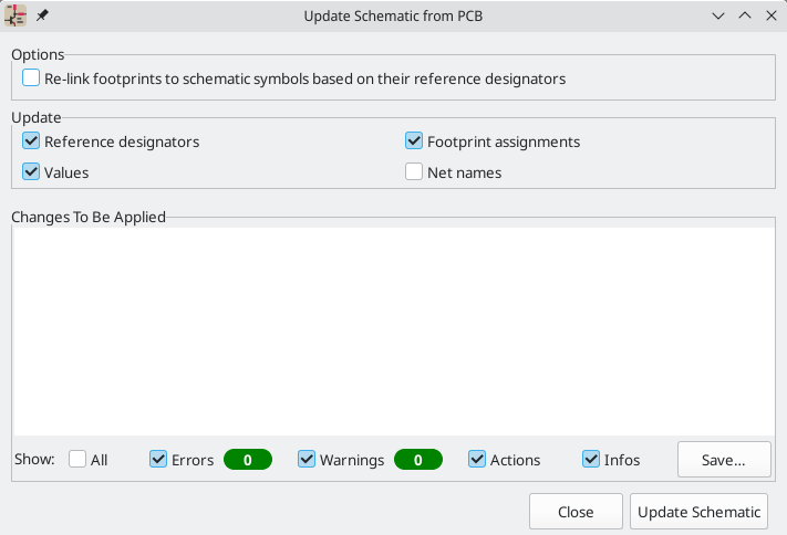
The tool syncs changes in reference designators, values, footprint assignments, and net names from the board to the schematic. Each type of change can be individually enabled or disabled.
The changes that will be made to the schematic are listed in the Changes To Be Applied pane. The schematic is not modified until you click the Update Schematic button.
You can show or hide different types of messages using the checkboxes at the bottom of the window. A report of the changes can be saved to a file using the Save… button.
Options
The tool has several options to control its behavior.
Option |
Description |
Re-link footprints to schematic symbols based on their reference designators |
If checked, each footprint in the PCB will be re-linked to the symbol that has the same reference designator as the footprint. This option is incompatible with updating symbol reference designators. If unchecked, footprints and symbols will be linked by unique identifier as usual, rather than by reference designator. |
Reference designators |
If checked, symbol reference designators will be updated to match the reference designators of the linked footprints. If unchecked, symbol reference designators will not be updated. |
Values |
If checked, symbol values will be updated to match the values of the linked footprints. If unchecked, symbol values will not be updated. |
Footprint assignments |
If checked, footprint assignments will be updated for symbols which have had their footprints changed or replaced in the board. If unchecked, symbol footprint assignments will not be updated. |
Net names |
If checked, the schematic will be updated with any net name changes that have been made in the board. Net labels will be updated or added to the schematic as necessary to match the board. If unchecked, net names will not be updated in the schematic. |
| The Geographical Reannotation feature can be used in combination with backannotating reference designators to reannotate all components in the design based on their location in the layout. |
Back annotation with CMP files
Select changes can also be synced from the PCB back to the schematic by exporting a CMP file from the PCB editor (File → Export → Footprint Association (.cmp) File…) and importing it in the Schematic Editor (File → Import → Footprint Assignments…).
| This method can only sync changes made to footprint assignments and footprint fields. It is recommended to use the Update Schematic from PCB tool instead. |
Geographical re-annotation
| This section of the KiCad documentation has not yet been written. We appreciate your patience as our small team of volunteer documentation writers work to update and expand the documentation. |
Locking
Most objects can be locked through their properties dialogs, by using the right-click context menu, or by using the Toggle Lock hotkey (L). Locked objects cannot be selected unless the "Locked items" checkbox is enabled in the selection filter. Attempting to move locked items will result in a warning dialog:
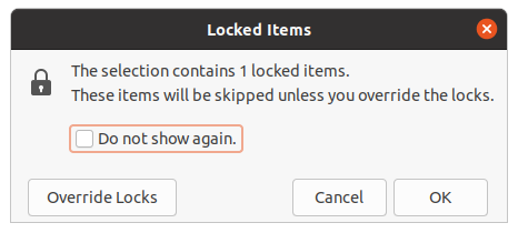
Selecting "Override Locks" in this dialog will allow moving the locked items. Selecting "OK" will allow you to move any unlocked items in the selection; leaving the locked items behind. Selecting "Do not show again" will remember your choice for the rest of your session.
Bulk editing tools
| This section of the KiCad documentation has not yet been written. We appreciate your patience as our small team of volunteer documentation writers work to update and expand the documentation. |
Cleanup tools
| This section of the KiCad documentation has not yet been written. We appreciate your patience as our small team of volunteer documentation writers work to update and expand the documentation. |
Importing graphics
| This section of the KiCad documentation has not yet been written. We appreciate your patience as our small team of volunteer documentation writers work to update and expand the documentation. |
Importing vector drawings from DXF and SVG files
| This section of the KiCad documentation has not yet been written. We appreciate your patience as our small team of volunteer documentation writers work to update and expand the documentation. |
Importing bitmap images
| This section of the KiCad documentation has not yet been written. We appreciate your patience as our small team of volunteer documentation writers work to update and expand the documentation. |
Inspecting a board
Measurement tool
The measurement tool allows you to make distance and angle measurements between points on the PCB.
To activate the tool, click the ![]() icon in the right toolbar,
or use the hotkey Ctrl+Shift+M. Once the tool is active, click once to set the
measurement start point, then click again to finish a measurement.
icon in the right toolbar,
or use the hotkey Ctrl+Shift+M. Once the tool is active, click once to set the
measurement start point, then click again to finish a measurement.
| The measurement tool is used for quick measurements that do not need to be displayed permanently. Any measurement you make will only be shown while the tool is active. To create permanent dimensions that will appear in printouts and plots, use the Dimension tools. |
Design rule checking
The design rule checker is used to verify that the PCB meets all the requirements established in the Board Setup dialog and that all pads are connected according to the netlist or schematic. KiCad can automatically prevent some design rule violations while routing tracks, but many others cannot be prevented automatically. This means it is important to use the design rule checker before creating manufacturing files for a PCB.
To use the design rule checker, click the ![]() icon in the top toolbar,
or select Design Rules Checker from the Inspect menu.
icon in the top toolbar,
or select Design Rules Checker from the Inspect menu.
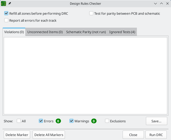
The top section of the DRC Control window contains some options that control the design rule checker:
Refill all zones before performing DRC: when enabled, zones will be refilled every time the design rule checker is run. Disabling this option may result in incorrect DRC results if zones have not been refilled manually.
Report all errors for each track: when enabled, all clearance errors will be reported for each track segment. When disabled, only the first error will be reported. Enabling this option will result in the design rule checker running more slowly.
Test for parity between PCB and schematic: when enabled, the design rule checker will test for differences between the schematic and PCB in addition to testing the PCB design rules. This option has no effect when running the PCB editor in standalone mode.
After running DRC, any violations will be shown in the center part of the DRC Control window. Rule violations, unconnected items, and differences between the schematic and the PCB are shown in three different tabs. The controls below the list of violations can be used to show or hide violations depending on their severity. A report file in plain text format can be created after running DRC using the Save button.
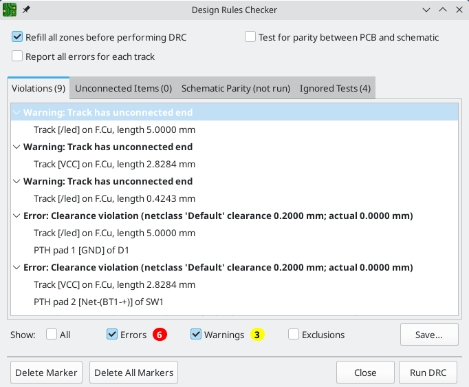
Each violation involves one or more objects on the PCB. In the list of violations, the objects involved are listed below the violation. Clicking on the violation in the list view will move the PCB Editor view so that the affected area is centered. Clicking on one of the objects involved in a violation will highlight the object.
The numbers at the bottom of the window show the number of errors, warnings, and exclusions. Each type of violation can be filtered from the list using the respective checkboxes. Clicking Delete Markers will clear all violations until DRC is run again.
Violations can be right-clicked in the dialog to ignore them or change their severity:
-
Exclude this violation: ignores this particular violation, but does not affect any other violations.
-
Change severity: changes a type of violation from warning to error, or error to warning. This affects all violations of a given type.
-
Ignore all: ignores all violations of a given type. This test will now appear in the Ignored Tests tab rather than the Violations tab.
Excluded and ignored violations are remembered between runs of the design rule checker.
Clearance and constraint resolution
The clearance and constraint resolution tools allow you to inspect which clearance and design constraint rules apply to selected items. These tools can help when designing PCBs with complex design rules where it is not always clear which rules apply to an object.
To inspect the clearance rules that apply between two objects, select both objects and choose Clearance Resolution from the Inspect menu. The Clearance Report dialog will show the clearance required between the objects on each copper layer, as well as the design rules that resulted in that clearance.
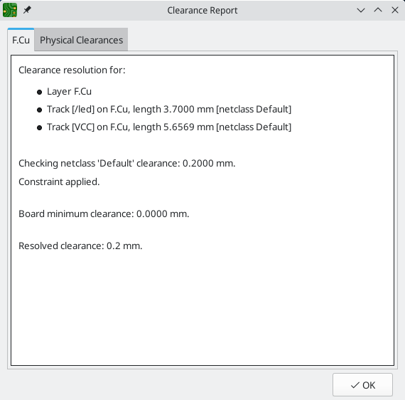
To inspect the design constraints that apply to an object, select it and choose Constraints Resolution from the Inspect menu. The Constraints Report dialog will show any constraints that apply to the object.
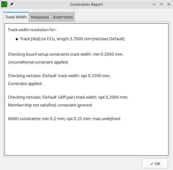
Find tool
The Find tool searches for text in the PCB, including reference designators,
footprint fields, and graphic text. When the tool finds a match, the canvas is
zoomed and centered on the match and the text is highlighted. Launch the tool
using the (![]() ) button in the top toolbar.
) button in the top toolbar.
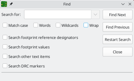
The Find tool has several options:
Match case: Selects whether the search is case-sensitive.
Words: When selected, the search will only match the search term with complete words in the PCB. When unselected, the search will match if the search term is part of a larger word in the PCB.
Wildcards: When selected, wildcards can be used in the search terms. ?
matches any single character, and * matches any number of characters. Note
that when this option is selected, partial matches are not returned: searching
for abc* will match the string abcd, but searching for abc will not.
Wrap: When selected, search results will return to the first hit after reaching the last hit.
Search footprint reference designators: Selects whether the search should apply to footprint reference designators.
Search footprint values: Selects whether the search should apply to footprint value fields.
Search other text items: Selects whether the search should apply to other text items, including graphical text and footprint fields other than value and reference.
Search DRC markers: Selects whether the search should apply to the violation descriptions of DRC markers shown on the board.
Search panel
| This section of the KiCad documentation has not yet been written. We appreciate your patience as our small team of volunteer documentation writers work to update and expand the documentation. |
3D Viewer
The 3D Viewer shows a 3-dimensional view of the board and the components on the board. You can view the board from different perspectives, show or hide different types of components, cross-probe from the PCB Editor to the 3D viewer, and generate raytraced renders of the board.
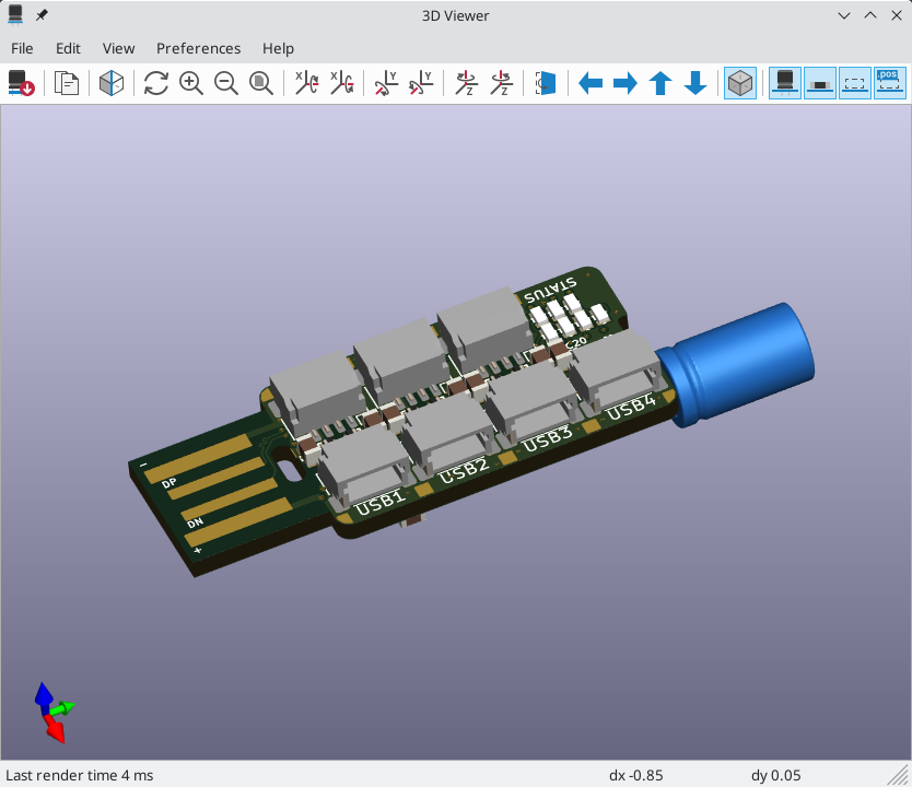
| The 3D model for a component will only appear if the 3D model file exists and has been assigned to the footprint. |
| Many footprints in KiCad’s standard library do not yet have model files created for them. However, these footprints may contain a path to a 3D model that does not yet exist, in anticipation of the 3D model being created in the future. |
Navigating the 3D view
Dragging with the left mouse button will orbit the 3D view. By default this is the centroid of the board, but the pivot point can be reset to a new point on the board by moving the cursor over the desired point and pressing Space. Scrolling the mouse wheel will zoom the view in or out. Scrolling while holding Ctrl pans the view left and right, and scrolling while holding Shift pans up and down. Dragging with the middle mouse button also pans the view.
Different sized 3D grids can be set using the Preferences → 3D Grid menu. Bounding boxes for each component can be enabled with Preferences → Show Model Bounding Boxes.
When the PCB Editor and the 3D Viewer are both open, selecting a footprint in the PCB Editor will also highlight the component in the 3D Viewer. The highlight color is adjustable in Preferences → Preferences… → 3D Viewer → Realtime Renderer → Selection Color.
Generating images with the 3D Viewer
The current 3D view can be saved to an image with File → Export Current
View as PNG… or Export Current View as JPG…, depending on the desired
image format. The current view can also be copied to the clipboard using the
![]() button, or Edit → Copy 3D
Image.
button, or Edit → Copy 3D
Image.
The 3D Viewer has a raytracing rendering mode which displays the board using a
more physically accurate rendering model than the default rendering mode.
Raytracing is slower than the default rendering mode, but it can be used when
the most visually attractive results are desired. Raytracing mode is enabled
with the ![]() button, or with
Preferences → Raytracing. The 3D grid and selection highlights are not
shown in raytracing mode.
button, or with
Preferences → Raytracing. The 3D grid and selection highlights are not
shown in raytracing mode.
Colors and other rendering options, for both raytraced and non-raytraced modes, can be adjusted in Preferences → Preferences… → 3D Viewer.
3D viewer controls
Many viewing options are controlled with the top toolbar.
|
Reload the 3D model |
|
Copy 3D image to clipboard |
|
Render current view using raytracing |
|
Redraw |
|
Zoom in |
|
Zoom out |
|
Fit drawing in display area |
|
Rotate X clockwise |
|
Rotate X counterclockwise |
|
Rotate Y clockwise |
|
Rotate Y counterclockwise |
|
Rotate Z clockwise |
|
Rotate Z counterclockwise |
|
Flip board view |
|
Pan board left |
|
Pan board right |
|
Pan board up |
|
Pan board down |
|
Enable/disable orthographic projection |
|
Show/hide 3D models for through-hole components |
|
Show/hide 3D models for surface mount components |
|
Show/hide 3D models for components of type 'other' |
|
Show/hide 3D models for components not in position file |
Net inspector
The Net Inspector allows you to view statistics about all the nets in a board. To open the
inspector, click the ![]() icon at the top of the Nets section of
the Appearance panel, or select Net Inspector from the Inspect menu.
icon at the top of the Nets section of
the Appearance panel, or select Net Inspector from the Inspect menu.
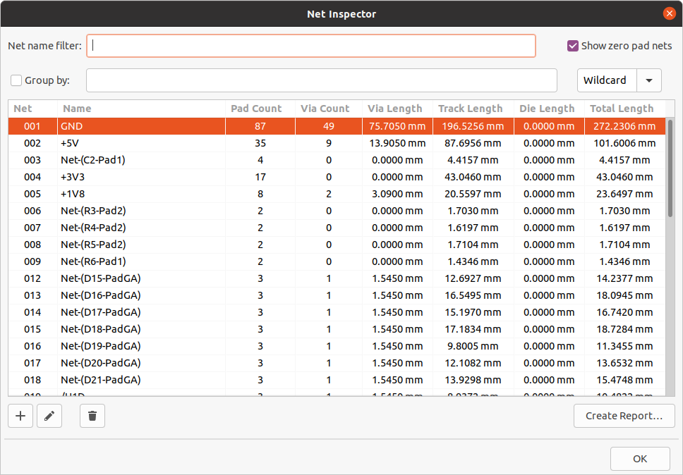
Clicking a net in the list will highlight that net on the board. Clicking a column title allows you to sort the list of nets by that column.
The Group By field allows you to combine different nets together and view the total length of the
combined nets. For example, if you have two nets named DATA0 and DATA0_EXT, using a Group By
value of DATA0* will create a group containing both nets. More complicated groupings can be
created by changing the Group By mode from Wildcard to RegEx (regular expressions). The substring
(Substr) variants of the Group By mode will create groups for each set of nets that matches the
pattern differently.
For example, if you have the nets U1D+, U1D-, U2D+, and U2D-, the grouping pattern U*D
will match all four nets in Wildcard mode, creating a single group U*D. In Wildcard Substr mode,
it will match all four nets, but create two different groups: U1D and U2D.
Pad Count and Via Count show the number of pads (surface mount and through hole) and vias on a net. Via Length shows the total height of each via (not accounting for which copper layers the via connects to). In other words, Via Length is equal to Via Count multiplied by the stackup height of the board. Track Length shows the total length of all track segments in a net, not accounting for topology. Die length shows the total of all Pad to Die Length values set for pads on the net.
| The lengths shown in the Net Inspector differ from those shown in the length tuning tools, because the Net Inspector shows the sum of all tracks connected to a net, and the length tuning tools show the distance between the closest two pads or branching vias. See the Routing section for more information about the length tuner. |
Generating outputs
KiCad can generate and export files in a number of different formats useful for manufacturing PCBs and interfacing with external software. This functionality is available in the File menu in a few different sections. The Fabrication Outputs section contains the most common operations needed to prepare a PCB for fabrication. The Export section contains tools for generating files that can be read by external software. The Plot function allows you to export 2D line drawings of the PCB in various formats. The Print function allows you to send a view of the PCB to a 2D printer.
Fabrication outputs and plotting
KiCad uses Gerber files as its primary plotting format for PCB manufacturing. To create Gerber files, open the Plot dialog from the File menu, or select Gerbers from the Fabrication Outputs section of the File menu. The Plot dialog will open, allowing you to configure and generate Gerber files.
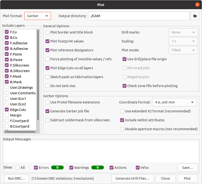
Plotting options
Include Layers: Check that every layer used on your board is enabled in the list. Disabled layers will not be plotted.
Output directory: Specify the location to save plotted files. If this is a relative path, it is created relative to the project directory.
Plot border and title block: If enabled, the drawing sheet border and title block will be plotted on each layer. This should usually be disabled when plotting Gerber files.
Plot footprint values: If enabled, the Value field of each footprint will be plotted on whatever layer it exists on (unless the field visibility is disabled for a specific footprint).
Plot reference designators: If enabled, the Reference Designator field of each footprint will be plotted on whatever layer it exists on (unless the field visibility is disabled for a specific footprint).
Force plotting of invisible values / refs: If enabled, all footprint values and reference designators will be plotted, even if the field visibility is disabled for some of these fields.
Plot Edge.Cuts on all layers: If enabled, the Edge.Cuts (board outline) layer will be added to all other layers. Check with your manufacturer to see what the correct value of this setting is for their manufacturing process.
Sketch pads on fabrication layers: If enabled, footprint pads on fabrication (F.Fab, B.Fab) layers will be drawn as unfilled outlines rather than filled shapes.
Do not tent vias: If enabled, vias will be left uncovered on the solder mask layers (F.Mask, B.Mask). If disabled, vias will be covered by solder mask (tented).
| KiCad does not support tenting or uncovering specific vias. Tenting may only be controlled globally (for all vias on a board). |
Drill marks: For plot formats other than Gerber, marks may be plotted at the location of all drilled holes. Drill marks may be created at the actual size (diameter) of the finished hole, or at a smaller size.
Scaling: For plot formats that support scaling other than 1:1, the plot scale may be set. The Auto scaling setting will scale the plot to fit the specified page size.
Plot mode: For some plot formats, filled shapes may be plotted as outlines only (sketch mode).
Use drill/place file origin: When enabled, the coordinate origin for plotted files will be the drill/place file origin set in the board editor. When disabled, the coordinate origin will be the absolute origin (top left corner of the worksheet).
Mirrored plot: For some plot formats, the output may be mirrored horizontally when this option is set.
Negative plot: For some plot formats, the output may be set to negative mode. In this mode, shapes will be drawn for the empty space inside the board outline, and empty space will be left where objects are present in the PCB.
Check zone fills before plotting: When enabled, zone fills will be checked (and refilled if outdated) before generating outputs. Plot outputs may be incorrect if this option is disabled!
Gerber options
Use Protel filename extensions: When enabled, the plotted Gerber files will be named with file
extensions based on Protel (.GBL, .GTL, etc). When disabled, the files will have the .gbr
extension.
Generate Gerber job file: When enabled, a Gerber job file (.gbrjob) will be generated along
with any Gerber files. The Gerber job file is an extension to the Gerber format that includes
information about the PCB stackup, materials, and finish. More information about Gerber job files
is available at the Ucamco website.
Coordinate format: Configure how coordinates will be stored in the plotted Gerber files. Check with your manufacturer for their recommended setting for this option.
Use extended X2 format: When enabled, the plotted Gerber files will use the X2 format, which includes information about the netlist and other extended attributes. This format may not be compatible with older CAM software used by some manufacturers.
Include netlist attributes: When enabled, the plotted Gerber files will include netlist information that can be used for checking the design in CAM software. When X2 format mode is disabled, this information is included as comments in the Gerber files.
Disable aperture macros: When enabled, all shapes will be plotted as primitives rather than by using aperture macros. This setting should only be used for compatibility with old or buggy CAM software when requested by your manufacturer.
PostScript options
Scale factor: Controls how coordinates in the board file will be scaled to coordinates in the PostScript file. Using a different value for X and Y scale factors will result in a stretched / distorted output. These factors may be used to correct for scaling in the PostScript output device to achieve an exact-scale output.
Track width correction: A global factor that is added (or subtracted, if negative) from the size of tracks, vias, and pads when plotting a PostScript file. This factor may be used to correct for errors in the PostScript output device to achieve an exact-scale output.
Force A4 output: When enabled, the generated PostScript file will be A4 size even if the KiCad board file is a different size.
SVG options
Units: Controls the units that will be used in the SVG file. Since the SVG format has no specified units system, you must export using the same units setting that you want to use for importing into other software.
Precision: Controls how many significant digits will be used to store coordinates.
DXF options
Plot graphic items using their contours: Graphic shapes in DXF files have no width. This option controls how graphic shapes with a width (thickness) in a KiCad board are plotted to a DXF file. When this option is enabled, the outer contour of the shape will be plotted. When this option is disabled, the centerline of the shape will be plotted (and the shape’s thickness will not be visible in the resulting DXF file).
Use KiCad font to plot text: When enabled, text in the KiCad design will be plotted as graphic shapes using the KiCad font. When disabled, text will be plotted as DXF text objects, which will use a different font and will not appear in exactly the same position and size as shown in the KiCad board editor.
Export units: Controls the units that will be used in the DXF file. Since the DXF format has no specified units system, you must export using the same units setting that you want to use for importing into other software.
HPGL options
Default pen size: Controls the plotter pen size used to create graphics.
Drill files
KiCad can generate CNC drilling files required by most PCB manufacturing processes in either Excellon or Gerber X2 format. KiCad can also generate a drill map: a graphical plot of the board showing drill locations. Select the Generate Drill Files option from the Fabrication Outputs menu to open the dialog:
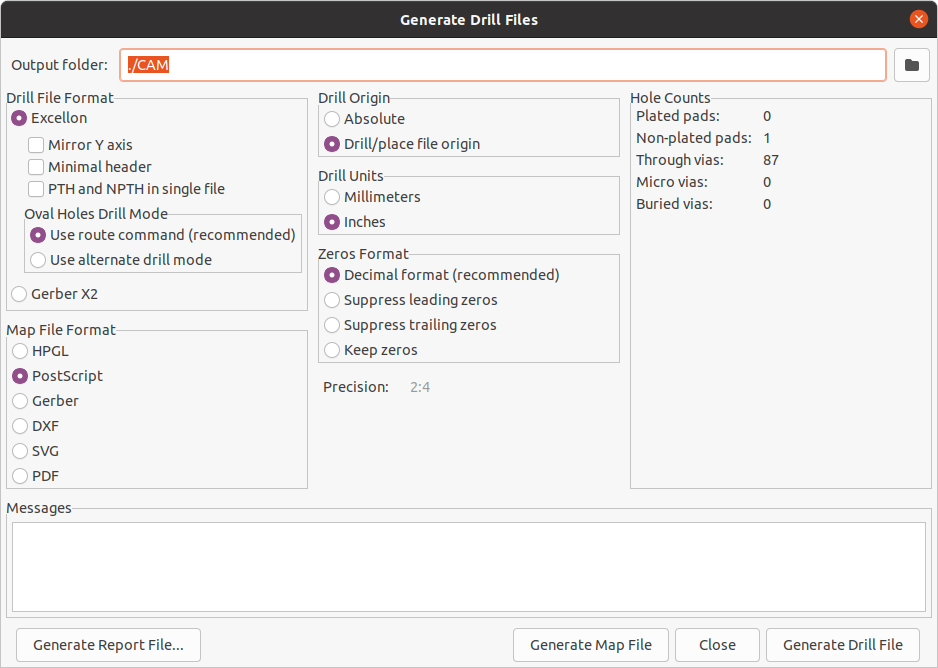
Output folder: Choose the folder to save generated drill and map files to. If a relative path is entered, it will be relative to the project directory.
Drill file format: Choose whether to generate Excellon drill files (required by most PCB manufacturers) or Gerber X2 files.
Mirror Y axis: For Excellon files, choose whether or not to mirror the Y-axis coordinate. This option should in general not be used when having PCBs manufactured by a third party, and is provided for convenience for users who are making PCBs themselves.
Minimal header: For Excellon files, choose whether to output a minimal header rather than a full file header. This option should not be enabled unless requested by your manufacturer.
PTH and NPTH in single file: By default, plated holes and non-plated holes will be generated in two different Excellon files. With this option enabled, both will be merged into a single file. This option should not be enabled unless requested by your manufacturer.
Oval holes drill mode: Controls how oval holes are represented in an Excellon drill file. The default setting, Use route command, is correct for most manufacturers. Only choose the Use alternate drill mode setting if requested by your manufacturer.
Map file format: Choose the output format for plotting a drill map.
Drill origin: Choose the coordinate origin for drill files. Absolute will use the page origin at the top left corner. Drill/place file origin will use the origin specified in the board design.
Drill units: Choose the units for drill coordinates and sizes.
Zeros format: Controls how numbers are formatted in an Excellon drill file. Select an option here based on your manufacturer’s recommendations.
Component placement files
Component placement files are text files that list each component (footprint) on the board along with its center position and orientation. These files are usually used for programming pick-and-place machines, and may be required by your manufacturer if you are ordering fully-assembled PCBs.
| A footprint will not appear in generated placement files if the "Exclude from position files" option is enabled for that footprint. This may be used for excluding certain footprints that do not represent physical components to be assembled. |
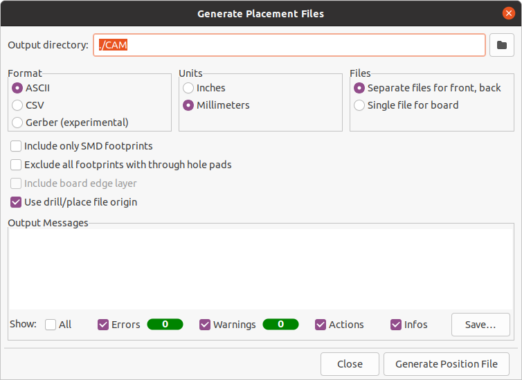
Format: Choose between generating a plain text (ASCII), comma-separated text (CSV), or Gerber placement file format.
Units: Choose the units for component locations in the placement file.
Files: Choose whether to generate separate files for footprints on the front and back of the board or a single file combining both sides.
Include only SMD footprints: When enabled, only footprints with the SMD fabrication attribute will be included. Check with your manufacturer to determine if non-SMD footprints should be included or excluded from the position file.
Exclude all footprints with through hole pads: When enabled, footprints will be excluded from the placement file if they contain any through-hole pads, even if their fabrication type is set to SMD.
Include board edge layer: For Gerber placement files, controls whether or not the board outline is included with the footprint placement data.
Use drill/place file origin: When enabled, component positions will be relative to the drill/place file origin set in the board design. When disabled, the positions will be relative to the page origin (upper left corner).
Additional fabrication outputs
KiCad can also generate footprint report files, IPC-D-356 netlist files, and a bill of materials (BOM) from the board design. These output formats have no configurable options.
Printing
KiCad can print the board view to a standard printer using the Print action in the File menu.
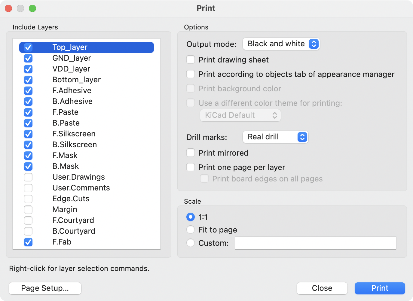
Include layers: Select the layers to include in the printout. Unselected layers will be invisible. Right-click the list for layer selection commands.
Output mode: Choose whether to print in black and white or full color.
Print drawing sheet: When enabled, the page border and title block will be printed.
Print according to objects tab of appearance manager: When enabled, any objects that have been hidden in the Objects tab of the Appearance panel will be hidden in the printout. When disabled, these objects will be printed if the layer they appear on is selected in the Included Layers area.
Print background color: When printing in full color, this option controls whether or not the view background color will be printed.
Use a different color theme for printing: When printing in full color, this option allows a different color theme to be used for printing. When disabled, the color theme used by the board editor will be used for printing.
Drill marks: Controls whether to show drilled holes at their actual size, at a small size, or hide them from the printout.
Print mirrored: When enabled, the printout will be mirrored horizontally.
Print one page per layer: When enabled, each layer selected in the Included Layers area will be printed to an individual page. If this option is enabled, the Print board edges on all pages option controls whether to add the Edge.Cuts layer to each printed page.
Scale: controls the scale of the printout relative to the page size configured in Page Setup.
Exporting files
KiCad can export a board design to various third-party formats for use with external software. These functions are found in the Export section of the File menu.
Specctra .DSN: creates a file suitable for importing into certain third-party autorouter software. This exporter has no configurable options.
| TODO: Document GenCAD exporter |
| TODO: Document VRML exporter |
IDF Exporter
The IDF exporter exports an
IDFv3 compliant
board (.emn) and library (.emp) file for communicating mechanical dimensions
to a mechanical CAD package. The exporter exports the board outline and cutouts,
all pad and mounting through holes including slotted holes, and component
outlines; this is the most basic set of mechanical data required for interaction
with mechanical designers. All other entities described in the IDFv3
specification are currently not exported.
| You must attach IDF component models to your design’s footprints before they will be included in the exported model. For more information on attaching models to footprints, see the footprint documentation. Some IDF-specific guidance is included in the Advanced Topics documentation. |
| For more information on creating IDF component models, including descriptions of the IDF utility tools included with KiCad, see the Advanced Topics documentation. |
Once models have been specified for all desired components, the model of the board can be exported. In the PCB Editor, select File → Export → IDFv3….

Grid reference point: Choose where the exported model’s reference point should be. If the Adjust automatically option is selected, KiCad will set the reference point to the centroid of the PCB. Otherwise, the reference point is set relative to the display origin.
Output units: Choose whether the exported model’s units are millimeters or mils.
The outputs can be viewed directly in a mechanical CAD application or converted
to VRML using the idf2vrml tool.
| TODO: Document STEP exporter |
| TODO: Document SVG exporter |
| TODO: Document CMP file exporter |
Hyperlynx: creates a file suitable for importing into Mentor Graphics (Siemens) HyperLynx simulation and analysis software.
Footprints and footprint libraries
Managing footprint libraries
KiCad’s footprint library management system allows directly using several types of footprint libraries:
-
KiCad
.prettyfootprint libraries (folders with .pretty extension, containing .kicad_mod files) -
KiCad Legacy footprint libraries (.mod files)
-
GEDA libraries (folders containing .fp files)
-
Eagle footprint libraries
KiCad only supports writing to KiCad’s native .pretty format footprint
libraries (and the .kicad_mod footprint files within them). All other
footprint library formats are read-only.
|
KiCad uses a table of footprint libraries to map footprint libraries of any supported library type to a library nickname. KiCad uses a global footprint library table as well as a table specific to each project. To edit either footprint library table, use Preferences → Manage Footprint Libraries….
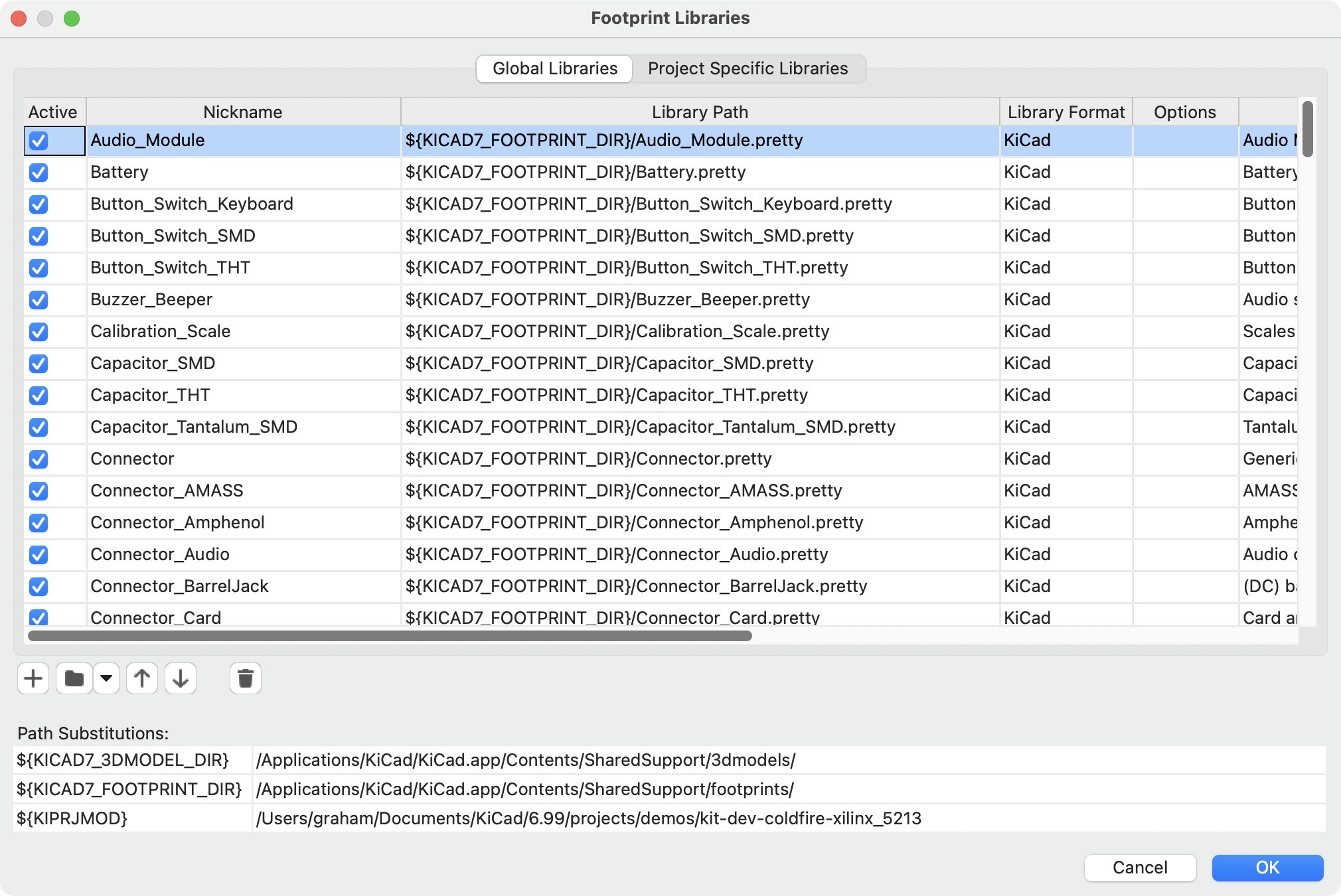
The global footprint library table contains the list of libraries that are
always available regardless of the currently loaded project. The table is
saved in the file fp-lib-table in the KiCad configuration folder.
The location of this folder
depends on the operating system being used.
The project specific footprint library table contains the list of libraries that
are available specifically for the currently loaded project. If there are any
project-specific footprint libraries, the table is saved in the file
fp-lib-table in the project folder.
Initial Configuration
The first time the PCB Editor (or any other KiCad tool that uses footprints) runs
and the global footprint table file fp-lib-table is not found, KiCad will
guide the user through setting up a new footprint library table. This process is
described above.
Managing Table Entries
Footprint libraries can only be used if they have been added to either the global or project-specific footprint library table.
Add a library either by clicking the
![]() button and selecting a
library or clicking the
button and selecting a
library or clicking the ![]() button
and typing the path to a library file. The selected library will be added to the
currently opened library table (Global or Project Specific). Libraries can be
removed by selecting desired library entries and clicking the
button
and typing the path to a library file. The selected library will be added to the
currently opened library table (Global or Project Specific). Libraries can be
removed by selecting desired library entries and clicking the
![]() button.
button.
The ![]() and
and
![]() buttons move the selected
library up and down in the library table. This does not affect the display order
of libraries in the Footprint Library Browser, Footprint Editor, or Add
Footprint tool.
buttons move the selected
library up and down in the library table. This does not affect the display order
of libraries in the Footprint Library Browser, Footprint Editor, or Add
Footprint tool.
Libraries can be made inactive by unchecking the Active checkbox in the first column. Inactive libraries are still in the library table but do not appear in any library browsers and are not loaded from disk, which can reduce loading times.
A range of libraries can be selected by clicking the first library in the range and then Shift-clicking the last library in the range.
Each library must have a unique nickname: duplicate library nicknames are not allowed in the same table. However, nicknames can be duplicated between the global and project library tables. Libraries in the project table take precedence over libraries with the same name in the global table.
Library nicknames do not have to be related to the library filename or path. The
colon character (:) cannot be used in library nicknames or footprint names
because it is used as a separator between nicknames and footprints.
Each library entry must have a valid path. Paths can be defined as absolute, relative, or by environment variable substitution.
The appropriate library format must be selected in order for the library to be
properly read. KiCad supports reading KiCad (.pretty), KiCad legacy (.mod),
Eagle (.lbr), and GEDA (folder with .fp files) footprint libraries.
There is an optional description field to add a description of the library entry. The option field is not used at this time so adding options will have no effect when loading libraries.
Environment Variable Substitution
The footprint library tables support environment variable substitution, which
allows you to define environment variables containing custom paths to where your
libraries are stored. Environment variable substitution is supported by using
the syntax ${ENV_VAR_NAME} in the footprint library path.
By default, KiCad defines several environment variables which are described in the project manager documentation. Environment variables can be configured in the Preferences → Configure Paths… dialog.
Using environment variables in the footprint library tables allows libraries to be relocated without breaking the footprint library tables, so long as the environment variables are updated when the library location changes.
${KIPRJMOD} is a special environment variable that always expands to the
absolute path of the current project directory. ${KIPRJMOD} allows libraries
to be stored in the project folder without having to use an absolute path in the
project library table. This makes it possible to relocate projects without
breaking their project library tables.
Using the GitHub Plugin
| KiCad removed support for the GitHub library plugin in version 6.0. |
Creating and editing footprints
| This section of the KiCad documentation has not yet been written. We appreciate your patience as our small team of volunteer documentation writers work to update and expand the documentation. |
Custom pad shapes
Footprint attributes
| Mention net ties here |
Footprint wizards
For more information about creating new footprint wizards, see the Scripting section of the Advanced Topics chapter.
Advanced topics
Configuration and Customization
The KiCad PCB Editor has a variety of preferences that can be configured through the Preferences dialog. Like all parts of KiCad, the preferences for the PCB Editor are stored in the user configuration directory and are independent between KiCad minor versions to allow multiple versions to run side-by-side with independent preferences.
The first sections of the Preferences dialog (Common, Mouse and Touchpad, and Hotkeys) are shared between all KiCad programs. These sections are described in detail in the KiCad manual under the "Common preferences" section.
Display options
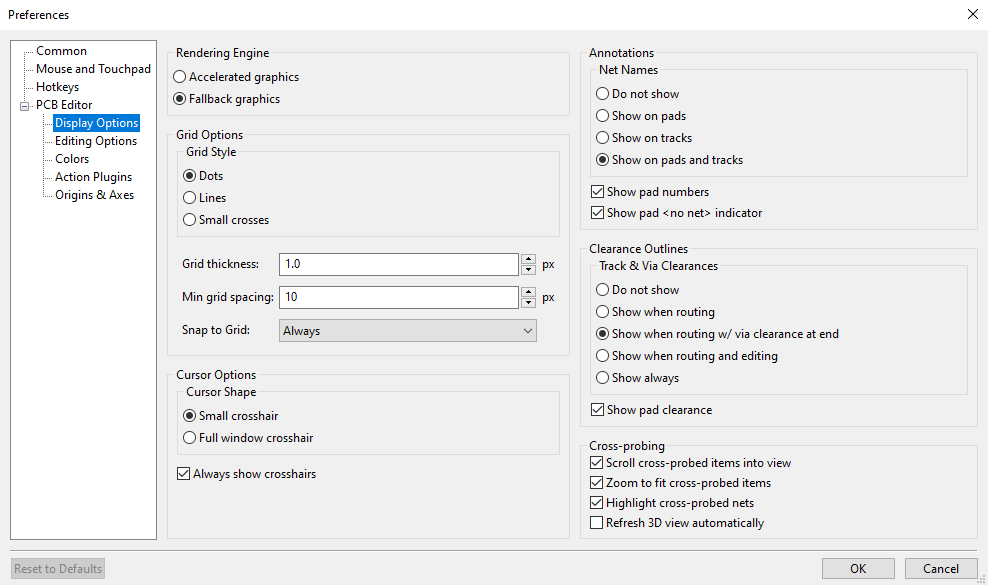
Rendering Engine: Controls if Accelerated graphics or Fallback graphics are used.
Grid style: Controls how the alignment grid is drawn.
Grid thickness: Controls how thick grid lines or dots are drawn.
Min grid spacing: Controls the minimum distance, in pixels, between two grid lines. Grid lines that violate this minimum spacing will not be drawn, regardless of the current grid setting.
Snap to grid: Controls when drawing and editing operations will be snapped to coordinates on the active grid. "Always" will enable snapping even when the grid is hidden; "When grid shown" will enable snapping only when the grid is visible.
| Grid snapping can be temporarily disabled by holding down Ctrl. |
Cursor shape: Controls whether the editing cursor is drawn as a small crosshair or a full-screen crosshair (a set of lines covering the entire drawing canvas). The editing cursor shows where the next drawing or editing action will occur and will be snapped to a grid location if snapping is enabled.
Always show crosshairs: Controls whether the editing cursor is shown all the time or only when an editing or drawing tool is active.
Net names: Controls whether or not net name labels are drawn on copper objects. These labels are guides for editing only and do not appear in fabrication outputs.
Show pad numbers: Controls whether or not pad number labels are drawn on footprint pads.
Show pad <no net> indicator: Controls whether or not pads with no net are indicated with a special marker.
Track clearance: Controls whether or not clearance outlines around tracks and vias are shown. Clearance outlines are shown as thin shapes around objects that indicate the minimum clearance to other objects, as defined by constraints and design rules.
Show pad clearance: Controls whether or not clearance outlines around pads are shown.
Center view on cross-probed items: When the Schematic and PCB Editors are both running, controls whether clicking a component or pin in Eeschema will center the PCB Editor view on the corresponding footprint or pad.
Zoom to fit cross-probed items: Controls whether the view will be zoomed to show a cross-probed footprint or pad.
Highlight cross-probed nets: Controls whether or not nets highlighted in Eeschema will be highlighted in the PCB Editor when the highlight tool is activated in both tools.
Editing options
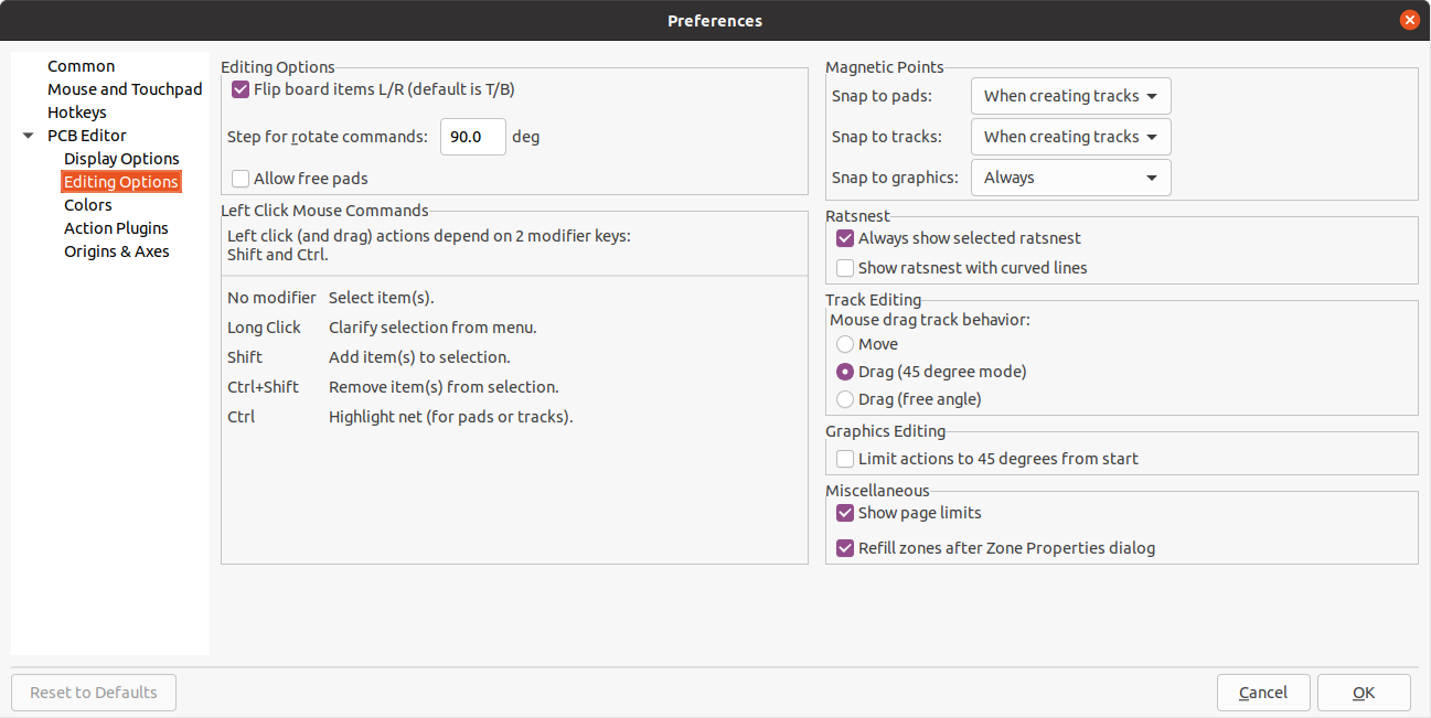
Flip board items L/R: Controls the direction board items will be flipped when moving them between the top and bottom layers. When checked, items are flipped Left-to-Right (about the Vertical axis); when unchecked, items are flipped Top-to-Bottom (about the Horizontal axis).
Step for rotate commands: Controls how far the selected object(s) will be rotated each time the Rotate command is used.
Allow free pads: Controls whether or not the pads of footprints can be unlocked and edited or moved separately from the footprint.
Magnetic points: This section controls object snapping, also called magnetic points. Object snapping takes precedence over grid snapping when it is enabled. Object snapping only works to objects on the active layer. Hold Shift to temporarily disable object snapping.
Snap to pads: Controls when the editing cursor will snap to pad origins.
Snap to tracks: Controls when the editing cursor will snap to track segment endpoints.
Snap to graphics: Controls when the editing cursor will snap to graphic shape points.
Always show selected ratsnest: When enabled, the ratsnest for a selected footprint will always be shown even if the global ratsnest is hidden.
Show ratsnest with curved lines: Controls whether ratsnest lines are drawn straight or curved.
Mouse drag track behavior: Controls the action that will occur when you drag a track segment with the mouse: "Move" will move the track segment independent of any others. "Drag (45 degree mode)" will invoke the push-and-shove router to drag the track, respecting design rules and keeping other track segments attached. "Drag (free angle)" will move the nearest corner of the track segment, highlighting collisions with other objects but not moving them out of the way.
Limit actions to 45 degrees from start Controls whether lines drawn with the graphic drawing tools can take on any angle. Note that this only affects drawing new lines: lines can be edited to take on any angle.
Show page limits: Controls whether or not the page boundary is drawn as a rectangle.
Refill zones after Zone Properties dialog: Controls whether or not zones are automatically refilled after editing the properties of any zone. This may be disabled on complicated designs or slower computers to improve responsiveness.
Colors
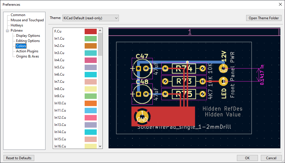
KiCad supports switching between different color themes to match your preferences. Kicad 7.0 comes with two built-in color themes: "KiCad Default" is a new theme designed to have good contrast and balance for most cases and is the default for new installations. "KiCad Classic" is the default theme from KiCad 5.1 and earlier versions. Neither of these built-in themes can be modified, but you can create new themes to customize the look of KiCad as well as install themes made by other users.
Color themes are stored in JSON files located in the colors subdirectory of the KiCad
configuration directory. The "Open Theme Folder" button will open this location in your system
file manager, making it easy to manage your installed themes. To install a new theme, place it in
this folder and restart KiCad. The new theme will be available from the drop-down list of color
themes if the file is a valid color theme file.
To create a new color theme, choose New Theme… from the drop-down list of color themes. Enter a name for your theme and then begin editing colors. The colors in the new theme will be copied from whatever theme was selected before you created the new theme.
To change a color, double-click or middle-click the color swatch in the list. The "Reset to Default" button will reset that color to its corresponding entry in the "KiCad Default" color theme.
Color themes are saved automatically; all changes are reflected immediately when you close the Preferences dialog. The window on the right side of the dialog shows a preview of how the selected theme will look.
Action plugins
The KiCad PCB editor supports plugins written in Python that can perform actions on the board being edited. These plugins can be installed using the built-in Plugin and Content Manager (see the KiCad chapter for details) or by placing the plugin files inside the user plugins directory. See the Scripting section below for details.
Each plugin that is detected will be shown in a row on this preferences page. Plugins may show a button on the top toolbar of the PCB editor. If the "Show button" control is unchecked for a plugin, it may still be accessed from the Tools > External Plugins menu.
The arrow controls at the bottom of the list allow changing the order that the plugins appear in the toolbar and menu. The folder button will launch a file explorer to the plugin folder, to make installing new plugins easier. The refresh button will scan the plugin folder for any new or removed plugins and update the list.
Origin & axes
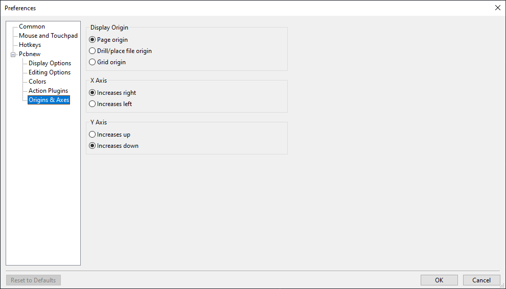
Display origin: Determines which coordinate origin is used for coordinate display in the editing canvas. The page origin is fixed at the corner of the page. The drill/place file origin and the grid origin can be moved by the user.
X axis: Controls whether X-coordinates increase to the right or to the left.
Y axis: Controls whether Y-coordinates increase upwards or downwards.
Text variables
KiCad supports text variables, which allow you to substitute the variable name
with a defined text string. This substitution happens anywhere the variable name
is used inside the variable replacement syntax of ${VARIABLENAME}.
You can define your own text variables in the schematic or board setup dialogs, but there are also a number of built-in system text variables. System text variables may be available in some contexts and not others.
The following variables can be used in PCB text, footprint text, and footprint fields. There are also a number of variables that can be used in the Schematic Editor.
| Variable name | Description |
|---|---|
|
Contents of drawing sheet’s |
|
Today’s date, in ISO format. |
|
Contents of drawing sheet’s |
|
Contents of drawing sheet’s |
|
Contents of drawing sheet’s |
|
Contents of drawing sheet’s |
|
Layer of the object. In footprint fields, this is the layer of the parent footprint. |
|
Contents of project text variable
|
|
Contents of footprint field Both built-in footprint fields and user-defined fields from the
corresponding symbol are available. Built-in footprint fields use all
uppercase letters: for example, to access a footprint’s value, use
Built-in footprint fields are |
|
Contents of field Both built-in footprint fields and user-defined fields from the
corresponding symbol are available. Built-in footprint fields use all
uppercase letters: for example, to access the value of Built-in footprint fields are |
Custom design rules
KiCad’s custom design rule system allows creating design rules that are more specific than the generic rules available in the Constraints page of the Board Setup dialog. Custom design rules have many applications, but in general they are used to apply certain rules to a portion of the board, such as a specific net or netclass, a specific area, or a specific footprint.
Custom design rules are stored in a separate file with the extension kicad_dru. This file is
created automatically when you start adding custom rules to a project. If you are using custom
rules in your project, make sure to save the kicad_dru file along with the kicad_pcb and
kicad_pro files when making backups or committing to a version control system.
The kicad_dru file is managed automatically by KiCad and should not be edited with an
external text editor. Always use the Custom Rules page of the Board Setup dialog to edit
custom design rules.
|
The Custom Rules editor
The custom rules editor is located in the Board Setup dialog and provides a text editor for entering custom rules, a syntax checker that will test your custom rules and note any errors, and a syntax help dialog that contains a quick reference to the custom rules language and some example rules.
It is a good idea to use the Check rule syntax button after editing custom rules to make sure there are no syntax errors. Any errors in the custom rules will prevent the design rule checker from running.
Custom rule syntax
The custom design rule language is based on s-expressions and allows you to create design constraints that are not possible with the built-in constraints. Each design rule generally contains a condition defining what objects to match, and a constraint defining the rule to be applied to the matched objects.
The language uses parentheses (( and )) to define clauses of related tokens and values.
Parentheses must always be matched: for every ( there must be a matching ). Inside a clause,
tokens and values are separated by whitespace. By convention, a single space is used, but any
number of whitespace characters between tokens is acceptable. In places where text strings are
valid, strings without any whitespace may be quoted with " or ', or unquoted. Strings that
contain whitespace must always be quoted. Where nested quotes are required, a single level of
nesting is possible by using " for the outer quote character and ' for the inner (or vice
versa). Newlines are not required, but are typically used in examples for clarity.
In the syntax descriptions below, items in <angle brackets> represent tokens that must be present
and items in [square brackets] represent tokens that are optional or only sometimes required.
The Custom Rules file must start with a version header defining the version of the rules language.
As of KiCad 7.0, the version is 1. The syntax of the version header is (version <number>). So
in KiCad 7.0 the header should read:
(version 1)
After the version header, you can enter any number of rules. Rules are evaluated in reverse order, meaning the last rule in the file is checked first. Once a matching rule is found for a given set objects being tested, no further rules will be checked. In practice, this means that more specific rules should be later in the file, so that they are evaluated before more general rules.
For example, if you create one rule that limits the minimum clearance between tracks in the net
HV and tracks in any other net and a second rule that limits the minimum clearance for all
objects inside a certain rule area, make sure the first rule appears later in the custom rules file
than the second rule. Otherwise tracks in the HV net could have the wrong clearance if they fall
inside the rule area.
Each rule must have a name and one or more constraint clause. The name can be any string and is
used to refer to the rule in DRC reports. The constraint defines the behavior of the rule.
Rules may also have a condition clause that determines which objects should have the rule applied,
an optional layer clause, which specifies which board layers the rule applies to,
and an optional severity clause which specifies the severity of the resulting DRC violation.
(rule <name>
    [(severity <severity>)]
    [(layer <layer_name>)]
    [(condition <expression>)]
    (constraint <constraint_type> [constraint_arguments]))
The custom rules file may also include comments to describe rules. Comments are denoted by any
line that begins with the # character (not including whitespace). You can press Ctrl+/
to comment or uncomment lines automatically.
# Clearance for 400V nets to anything else
(rule HV
    (condition "A.NetClass == 'HV'")
    (constraint clearance (min 1.5mm)))
Layer Clause
The layer clause determines which layers the rule will work on. While the layer of objects can
be tested in the condition clause as described below, using the layer clause is more efficient.
The value of the layer clause can be any board layer name, or the shortcuts outer to match the
front and back copper layers (F.Cu and B.Cu) and inner to match any internal copper layers.
If the layer clause is omitted, the rule will apply to all layers.
Some examples:
# Do not allow footprints on back layer (no condition clause means this rule always applies)
(rule "Top side footprints only"
    (layer B.Cu)
    (constraint disallow footprint))

# This rule does the same thing, but is less efficient
(rule "Top side footprints only"
    (condition "A.Layer == 'B.Cu'")
    (constraint disallow footprint))

# Larger clearance on outer layers (inner layer clearance set by board minimum clearance)
(rule "clearance_outer"
    (layer outer)
    (constraint clearance (min 0.25mm)))
Severity Clause
The severity clause sets the DRC violation severity whenever the rule is violated.
Possible values are error, warning, ignore, and exclusion. Ignored rules are not observed by
the interactive router and violations are not shown in the DRC dialog. However, ignored rules are
evaluated for matching and therefore can still override earlier rules. Errors, warnings, and excluded
rules are all observed by the interactive router, and violations are displayed in the DRC dialog when
the appropriate filters are selected.
Setting a rule’s severity to ignore does not disable the rule; only the effects of the rule
are disabled. The rule is still evaluated and can still override previous rules.
|
Condition Clause
The rule condition is an expression contained inside a text string (and therefore usually surrounded by quotes in order to allow whitespace for clarity). The expression is evaluated against each pair of objects that is being tested by the design rule checker. For example, when checking for clearance between copper objects, each copper object (track segment, pad, via, etc.) on each net is checked against other copper objects on other nets. If a custom rule exists where the expression matches the two given copper objects and the constraint defines a copper clearance, this custom rule could be used to determine the required clearance between the two objects.
The objects being tested are referred to as A and B in the expression language. The order of
the two objects is not important because the design rule checker will test both possible orderings.
For example, you can write a rule that assumes that A is a track and B is a via. There are
some expression functions that test both objects together; these use AB as the object name.
The expression in a condition must resolve to a boolean value (true or false). If the
expression resolves to true, the rule is applied to the given objects.
Each object being tested has properties that can be compared, as well as functions that
can be used to perform certain tests. The syntax for using properties and functions is
<object>.<property> and <object>.<function>([arguments]) respectively.
When you type <object>. in the text editor (A., B., or AB.), an autocomplete list
will open that contains all the object properties that can be used.
|
The object properties and functions are compared using boolean operators to result in a boolean expression. The following operators are supported:
|
Equal to |
|
Not equal to |
|
Greater than, greater than or equal to |
|
Less than, less than or equal to |
|
And |
|
Or |
For example, A.NetClass == 'HV' will apply to any objects that are part of the "HV" netclass and
A.NetClass != B.NetClass will apply to any objects that are in different netclasses. Parentheses
can be used to clarify the order of operations in complex expressions but they are not required.
All the boolean operators have the same precedence and are evaluated in order from left to right.
Some properties represent a physical measurement, such as a size, angle, length, position, etc. On these properties, unit suffixes can be used in the custom rules language to specify what units are being used. If no unit suffix is used, the internal representation of the property will be used instead (nanometers for distances and degrees for most angles). The following suffixes are supported:
|
Millimeters |
|
Thousandths of an inch (mils) |
|
Inches |
|
Degrees |
|
Radians |
| The units used in custom design rules are independent of the display units in the PCB editor. |
Numeric conditions can use simple math expressions, for example
(condition "A.Hole_Size_X == 1.0mm + 0.1mm").
Constraints
The constraint clause of the rule defines the behavior of the rule on the objects that are
matched by the condition. Each constraint clause has a constraint type and one or more
arguments that set the behavior of the constraint. A single rule may have multiple constraint
clauses, in order to set multiple constraints (for example, clearance and track_width) for
objects that match the same rule conditions.
Many constraints take arguments that specify a physical measurement or quantity. These constraints
support minimum, optimal, and maximum value specification (abbreviated "min/opt/max"). The
minimum and maximum values are used for design rule checking: if the actual value is less
than the minimum or is greater than the maximum value in the constraint, a DRC error is created.
The optimal value is only used for some constraints, and informs KiCad of a "best" value to use
by default. For example, the optimal diff_pair_gap is used by the router when placing new
differential pairs. No errors will be created if the differential pair is later modified such that
the gap between the pair is different from the optimal value, as long as the gap is between the
minimum and maximum values (if these are specified). In all cases where a min/opt/max value is
accepted, any or all of the minimum, optimal, and maximum value can be specified.
Min/opt/max values are specified as (min <value>), (opt <value>), and (max <value>). For
example, a track width constraint may be written as
(constraint track_width (min 0.5mm) (opt 0.5mm) (max 1.0mm)) or simply
(constraint track_width (min 0.5mm)) if only the minimum width is to be constrained.
Numeric constraint values can use simple math expressions, for example
(constraint clearance (min 0.5mm + 0.1mm)).
| Constraint type | Argument type | Description |
|---|---|---|
|
min/opt/max |
Checks the width of annular rings on vias. |
|
boolean expression |
Checks that the boolean expression is true. If the expression is false, a DRC error will be created. The expression can use any of the properties listed in the Object Properties section. |
|
min |
Checks the clearance between copper objects of different nets. KiCad’s design rule system does not permit constraining clearance between objects on the same net at this time. To allow copper objects to overlap (collide), create a |
|
min |
Checks the width of connections between pads and zones. An error will be generated for each pad
connection that is narrower than the |
|
min |
Checks the clearance between footprint courtyards and generates an error if any two courtyards
are closer than the |
|
min/opt/max |
Checks the gap between coupled tracks in a differential pair. Coupled tracks are segments that are parallel to each other. Differential pair gap is not tested on uncoupled portions of a differential pair (for example, the fanout from a component). |
|
max |
Checks the distance that a differential pair track is routed uncoupled from the other polarity track in the pair (for example, where the pair fans out from a component, or becomes uncoupled to pass around another object such as a via). |
|
|
Specify one or more object types to disallow, separated by spaces. For example,
|
|
min/opt/max |
Checks the clearance between objects and graphical items on the |
|
min |
Checks the clearance between a drilled hole in a pad or via and copper objects on a different net. The clearance is measured from the diameter of the hole, not its center. |
|
min/max |
Checks the size (diameter) of a drilled hole in a pad or via. For oval holes, the smaller
(minor) diameter will be tested against the |
|
min |
Checks the clearance between mechanically-drilled holes in pads and vias. The clearance is measured between the diameters of the holes, not between their centers. HDI vias (microvias, blind vias, and buried vias) are not tested by this constraint. |
|
min/max |
Checks the total routed length for the nets that match the rule condition and generates an
error for each net that is below the |
|
|
Checks the total number of connections (spokes) to a pad. An error will be raised for each pad that has fewer than the specified number of spokes. |
|
min |
Checks the clearance between two objects on a given layer (including non-copper layers). While this can perform more general-purpose checks than |
|
min |
Checks the clearance between a drilled hole in a pad or via and another object, regardless of net. The clearance is measured from the diameter of the hole, not its center. This can also be thought of as the "drilling tolerance" as it only includes round holes
(see |
|
min/opt/max |
Checks the clearance between objects on silkscreen layers and other objects. |
|
max |
Checks the total skew for the nets that match the rule condition, that is, the difference
between the length of each net and the average of all the lengths of each net that is matched
by the rule. If the absolute value of the difference between that average and the length of
any one net is above the constraint |
|
min/max |
Checks the height of text, including text boxes. An error will be generated for each text item
that has a height below the |
|
min/max |
Checks the thickness of text, including text boxes. An error will be generated for each text
item that has a thickness below the |
|
min |
Specifies the width of the gap between a pad and a zone with a thermal-relief connection. |
|
opt |
Specifies the width of the spokes connecting a pad to a zone with a thermal-relief connection. |
|
min/opt/max |
Checks the width of track and arc segments. An error will be generated for each segment that
has a width below the |
|
max |
Counts the number of vias on every net matched by the rule condition. If that number exceeds
the constraint |
|
min/max |
Checks the diameter of vias. An error will be generated for each via that has a diameter below
the |
|
|
Specifies the connection to be made between a zone and a pad. |
Object property and function reference
The following properties can be tested in custom rule expressions:
Common Properties
These properties apply to all PCB objects.
| Property | Data type | Description |
|---|---|---|
|
string |
The board layer on which the object exists. For objects that exist on more than one layer,
this property will return the first layer (for example, |
|
boolean |
True if the object is locked. |
|
string |
Returns the unique identifier of the parent object of this object. |
|
dimension |
The position of the object’s origin in the X-axis. Note that the origin of an object is not always the same as the center of the object’s bounding box. For example, the origin of a footprint is the location of the (0, 0) coordinate of that footprint in the footprint editor, but the footprint may have been designed such that this location is not in the center of the courtyard shape. |
|
dimension |
The position of the object’s origin in the Y-axis. Note that KiCad always uses Y-coordinates that increase from the top to bottom of the screen internally, even if you have configured your settings to show the Y-coordinates increasing from bottom to top. |
|
string |
One of "Footprint", "Pad", "Graphic Shape", "Board Text", "Footprint Text", "Zone", "Track", "Via", "Zone", or "Group". |
Connected Object Properties
These properties apply to copper objects that can have a net assigned (pads, vias, zones, tracks).
| Property | Data type | Description |
|---|---|---|
|
integer |
The net code of the copper object. Note that net codes should not be relied upon to remain
constant: if you need to refer to a specific net in a rule, use |
|
string |
The name of the netclass for the copper object. |
|
string |
The name of the net for the copper object. |
Footprint Properties
These properties apply to footprints.
| Property | Data type | Description |
|---|---|---|
|
dimension |
The copper clearance override set for the footprint. |
|
string |
The "Description" from the library footprint. |
|
boolean |
True if the footprint’s "Do not populate" attribute is set. |
|
boolean |
True if the footprint’s "Exclude from position files" attribute is set. |
|
boolean |
True if the footprint’s "Exclude from bill of materials" attribute is set. |
|
boolean |
True if the footprint’s "Exempt from courtyard requirement" attribute is set. |
|
string |
The "Keywords" from the library footprint. |
|
string |
The link to the library footprint in |
|
boolean |
True if the footprint’s "Not in schematic" attribute is set. |
|
double |
The orientation (rotation) of the footprint in degrees. |
|
string |
The reference designator of the footprint. |
|
dimension |
The solder paste margin override set for the footprint. |
|
dimension |
The solder paste margin ratio override set for the footprint. |
|
dimension |
The thermal relief gap set for the footprint. |
|
dimension |
The thermal relief connection width set for the footprint. |
|
string |
The contents of the "Value" field of the footprint. |
|
string |
One of "Inherited", "None", "Thermal reliefs" or "Solid". |
Pad Properties
These properties apply to footprint pads.
| Property | Data type | Description |
|---|---|---|
|
dimension |
The copper clearance override set for the pad. |
|
string |
One of "None", "BGA pad", "Fiducial, global to board", "Fiducial, local to footprint", "Test point pad", "Heatsink pad", "Castellated pad". |
|
dimension |
The size of the pad’s drilled hole/slot in the X axis. |
|
dimension |
The size of the pad’s drilled hole/slot in the Y axis. |
|
double |
The orientation (rotation) of the pad in degrees. |
|
string |
The "number" of a pad, which can be a string (for example "A1" in a BGA). |
|
dimension |
The value of the "pad to die length" property of a pad, which is additional length added to the pad’s net when calculating net length. |
|
string |
One of "Through-hole", "SMD", "Edge connector", or "NPTH, mechanical". |
|
string |
The name of the pad (usually the name of the corresponding pin in the schematic). |
|
string |
The electrical type of the pad (usually taken from the corresponding pin in the schematic). One of "Input", "Output", "Bidirectional", "Tri-state", "Passive", "Free", "Unspecified", "Power input", "Power output", "Open collector", "Open emitter", or "Unconnected". |
|
double |
For rounded rectangle pads, the ratio of radius to rectangle size. |
|
string |
One of "Circle", "Rectangle", "Oval", "Trapezoid", "Rounded rectangle", "Chamfered rectangle", or "Custom". |
|
dimension |
The size of the pad in the X-axis. |
|
dimension |
The size of the pad in the Y-axis. |
|
dimension |
The solder mask margin override set for the pad. |
|
dimension |
The solder paste margin override set for the pad. |
|
dimension |
The solder paste margin ratio override set for the pad. |
|
dimension |
The thermal relief gap set for the pad. |
|
dimension |
The thermal relief connection angle set for the pad. |
|
dimension |
The thermal relief connection width set for the pad. |
|
string |
One of "Inherited", "None", "Thermal reliefs" or "Solid". |
Track and Arc Properties
These properties apply to tracks and arc tracks.
| Property | Data type | Description |
|---|---|---|
|
dimension |
The x-coordinate of the start point. |
|
dimension |
The y-coordinate of the start point. |
|
dimension |
The x-coordinate of the end point. |
|
dimension |
The y-coordinate of the end point. |
|
dimension |
The width of the track or arc. |
Via Properties
These properties apply to vias.
| Property | Data type | Description |
|---|---|---|
|
dimension |
The diameter of the via’s pad. |
|
dimension |
The diameter of the via’s finished hole. |
|
string |
The last layer in the via stackup. |
|
string |
The first layer in the via stackup. |
|
string |
One of "Through", "Blind/buried", or "Micro". |
Zone and Rule Area Properties
These properties apply to copper and non-copper zones, and rule areas (formerly called keepouts).
| Property | Data type | Description |
|---|---|---|
|
dimension |
The copper clearance override set for the zone. |
|
dimension |
The minimum allowed width of filled areas in the zone. |
|
string |
The user-specified name (blank by default). |
|
string |
One of "Inherited", "None", "Thermal reliefs", "Solid", or "Reliefs for PTH". |
|
integer |
The priority level of the zone. |
|
dimension |
The thermal relief gap set for the zone. |
|
dimension |
The thermal relief connection width set for the zone. |
Graphic Shape Properties
These properties apply to graphic lines, arcs, circles, rectangles, and polygons.
| Property | Data type | Description |
|---|---|---|
|
dimension |
The angle of an arc. |
|
dimension |
The x-coordinate of the end point. |
|
dimension |
The y-coordinate of the end point. |
|
boolean |
True if the shape is filled. |
|
dimension |
Thickness of the strokes of the shape. |
|
string |
One of "Segment", "Rectangle", "Arc", "Circle", "Polygon", or "Bezier". |
|
dimension |
The x-coordinate of the start point. |
|
dimension |
The y-coordinate of the start point. |
Text Properties
These properties apply to text objects (footprint fields, free text labels, etc).
| Property | Data type | Description |
|---|---|---|
|
boolean |
True if the text is bold. |
|
dimension |
Height of a character in the font. |
|
string |
Horizontal text justification (alignment): one of "Left", "Center", or "Right". |
|
boolean |
True if the text is italic. |
|
boolean |
True if the text has the knockout property set. |
|
boolean |
True if the text is mirrored. |
|
string |
The contents of the text object. |
|
dimension |
Thickness of the stroke of the font. |
|
dimension |
Width of a character in the font. |
|
string |
Vertical text alignment: one of "Top", "Center", or "Bottom". |
|
boolean |
True if the text object is visible (displayed). |
Expression functions
The following functions can be called on objects in custom rule expressions:
| Function | Objects | Description |
|---|---|---|
|
|
Returns true if all of the object is inside the named rule area or zone. Note that
|
|
|
Returns true if the object exists on the given board layer. |
|
|
Returns true if the object exists on the copper path between the given pads. |
|
|
Returns the value of field |
|
|
Returns true if the object is part of a differential pair and the base name of the pair
matches the given argument |
|
|
Returns true if any part of the object is inside the named rule area or zone. Rule area and zone names can be set in their respective properties dialogs. If the given area is a filled copper zone, the function tests if the given object is inside any of the filled copper regions of the zone, not if the object is inside the zone’s outline. Deprecated; use |
|
|
Returns true if the any part of the object is inside the courtyard of the given footprint reference. The
first variant checks both the front or back courtyard and returns true if the object is inside
either one; the second and third variants check a specific courtyard. The Deprecated; use |
|
|
Returns true if any part of the object is inside the named rule area or zone. Rule area and zone names can be set in their respective properties dialogs. If the given area is a filled copper zone, the function tests if the given object is inside any of the filled copper regions of the zone, not if the object is inside the zone’s outline. |
|
|
Returns true if the any part of the object is inside the courtyard of the given footprint reference. The
first variant checks both the front or back courtyard and returns true if the object is inside
either one; the second and third variants check a specific courtyard. The |
|
|
Returns true if the object is a blind/buried via. |
|
|
Returns true if the two objects being tested are part of the same differential pair but are
opposite polarities. For example, returns true if |
|
|
Returns true if the object is a microvia. |
|
|
Returns true if the object is a plated hole (in a pad or via). |
|
|
Returns true if the object is a member of the named group |
Custom design rule examples
(rule RF_width
	(layer outer)
	(condition "A.NetClass == 'RF'")
	(constraint track_width (min 0.35mm) (max 0.35mm)))

(rule "BGA neckdown"
	(constraint track_width (min 0.2mm) (opt 0.25mm))
	(constraint clearance (min 0.05mm) (opt 0.08mm))
	(condition "A.insideCourtyard('U3')"))

(rule "Distance between Vias of Different Nets"
	(constraint hole_to_hole (min 0.25mm))
	(condition "A.Type =='Via' && B.Type =='Via' && A.Net != B.Net"))

(rule "Distance between test points"
	(constraint courtyard_clearance (min 1.5mm))
	(condition "A.Reference =='TP*' && B.Reference == 'TP*"))

# This assumes that there is a cutout with 1mm thick lines
(rule "Clearance to cutout"
	(constraint clearance (min 0.8mm))
	(condition "A.Layer=='Edge.Cuts' && A.Thickness == 1.0mm"))

(rule "Max Drill Hole Size Mechanical"
	(constraint hole (max 6.3mm))
	(condition "A.Pad_Type == 'NPTH, mechanical'"))

(rule "Max Drill Hole Size PTH"
	(constraint hole (max 6.35mm))
	(condition "A.Pad_Type == 'Through-hole'"))

# Specify an optimal gap for a particular differential pair
(rule "Clock gap"
	(condition "A.inDiffPair('/CLK')")
	(constraint diff_pair_gap (opt 0.8mm)))

# Specify a larger clearance between differential pairs and anything else
(rule "Differential pair clearance"
	(condition "A.inDiffPair('*') && !AB.isCoupledDiffPair()")
	(constraint clearance (min 1.5mm)))
Scripting
Scripting allows you to automate tasks within KiCad using the Python language. It is possible to add functionality to KiCad through Python "action plugins" that can be added to the top toolbar. It is also possible to write standalone scripts that interact with KiCad files, for example, to generate fabrication outputs from a board file automatically.
This manual covers general scripting concepts. Users wishing to write or modify scripts should also use the Doxygen documentation located at https://docs.kicad.org/doxygen-python-7.0/namespaces.html.
KiCad 6 or newer requires Python 3 for scripting support. Python 2 is no longer supported.
Python script locations
Plugin scripts for the PCB editor can be installed automatically using the Plugin and Content
Manager (PCM), or manually by copying the plugin to a folder. Each plugin should be in its own
folder within the plugins folder. The location of the plugins folder is by default:
| Platform | Path |
|---|---|
Linx |
|
macOS |
|
Windows |
|
Action plugins
| This section of the KiCad documentation has not yet been written. We appreciate your patience as our small team of volunteer documentation writers work to update and expand the documentation. |
Footprint wizards
The footprint wizards are a collection of python scripts that can be accessed from the Footprint Editor. If you invoke the footprint dialog you select a given wizard that allows you to see the footprint rendered, and you have some parameters you can edit.
If the plugins are not properly distributed to your system package, you can find the latest versions in the KiCad source tree at gitlab.
Using the scripting console
The PCB Editor comes with a built-in Python console that can be used to inspect and interact with the
board. To launch the console, use the ![]() button in the top toolbar. The PCB Editor Python API is not automatically loaded, so to load it,
type
button in the top toolbar. The PCB Editor Python API is not automatically loaded, so to load it,
type import pcbnew into the console. The command pcbnew.GetBoard() will then return a
reference to the board currently loaded in the PCB Editor, which can be inspected and modified
through the console.
| TODO: Document the other useful PyAlaMode functions |
Writing external scripts
| This section of the KiCad documentation has not yet been written. We appreciate your patience as our small team of volunteer documentation writers work to update and expand the documentation. |
Writing action plugins
| This section of the KiCad documentation has not yet been written. We appreciate your patience as our small team of volunteer documentation writers work to update and expand the documentation. |
Working With IDF Component Outlines
KiCad can export an IDF representation of the board for use in mechanical CAD software. Below is some guidance on attaching IDF component outlines to footprints, creating new IDF component outlines, and a description of the IDF utilities included with KiCad.
Specifying component models for use by the exporter
IDF component models are attached to footprints using the footprint’s 3D model properties. The IDF exporter uses different filetypes than the 3D viewer and other 3D model exporters, so adding 3D models for the IDF exporter does not conflict with 3D models added to a footprint for other purposes.
To add an IDF model to a footprint in the footprint or PCB editors, edit the footprint’s properties and click on the 3D Models tab.
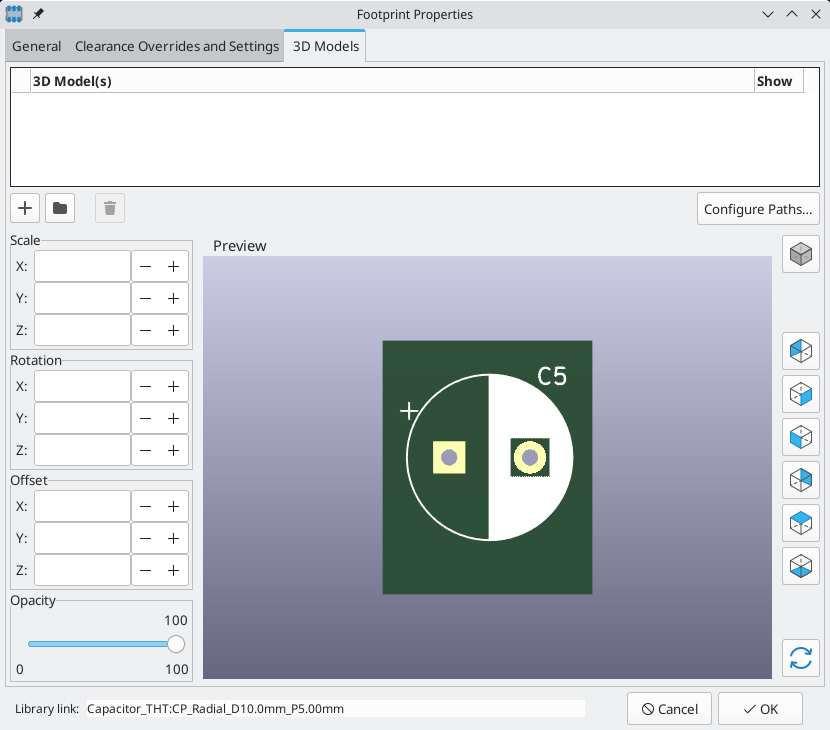
Click the ![]() button and select
the IDF (*.idf;*.IDF) filetype filter. Browse to the desired outline file.
button and select
the IDF (*.idf;*.IDF) filetype filter. Browse to the desired outline file.
Once the desired component outline file is selected, enter any necessary values for the offset and rotation. The offsets must be specified using the IDF board output units (mm or mils) and in the IDF coordinate system, which is a right-hand coordinate system with +Z pointing towards the viewer, +X to the viewer’s right, and +Y towards the upper edge of the screen. The rotation must be in degrees; positive rotation is a counter-clockwise rotation as described in the IDFv3 specification.
Multiple outlines may be combined with appropriate offsets to represent simple assemblies such as a DIP package in a socket.
| Only the offset values and the Z rotation value are used by the IDF exporter; all other values are ignored. |
Creating a component outline file
The component outline file (*.idf) consists of a single .ELECTRICAL or
.MECHANICAL section as described in the specification document. The section
may be preceded by any number of comment lines; the comment lines are copied by
the exporter into the library file and can be used to track metadata such as
references to the documents used to determine the component’s outline and
dimensions.
The component outline section contains fields which are strings, integers, or floating point numbers. A string is a combination of characters which may include spaces; if a string contains spaces then it must be quoted. Quotation marks must not appear within a string. Floating point numbers may be represented using decimal or exponential notations but decimal notation is preferred for human readability. The decimal point must be a dot and not a comma. The IDF file must consist only of 7-bit ASCII characters; use of 8-bit characters will result in undefined behavior.
An IDF file consists of SECTIONS which consist of RECORDS which consist of
FIELDS. For the IDF outline files only one type of section may exist and must be
one of .ELECTRICAL or .MECHANICAL. A record is a single line of text and may
contain one or more fields. Fields are sequences of characters separated by one
or more spaces which do not appear between quotation marks. All fields of a
record must appear on a single line; records may not span lines.
The section heading (.ELECTRICAL or .MECHANICAL) is considered the first
record (Record 1) of the section. Record 1 must be followed by Record 2
which has four fields:
-
Geometry Name: a string which in combination with the Part Number must form a unique identifier for the component outline. For standardized packages, the package name is a good value for the geometry name, for example "SOT-23". For unique packages the manufacturer’s part number is a good choice for the geometry name.
-
Part Number: although obviously intended for the part number, for example BS107, it is better to use this string to help describe the package. For example if the geometry name is "TO-92", the part number entry may be used to describe the layout of the pads or the orientation of this particular TO-92 outline file.
-
IDF Unit: this must be one of
MMorTHOUand it applies only to the units describing this single component outline. -
Height: this is a floating point number representing the nominal height of the component using units specified in Field 3.
Record 2 must be followed by a number of Record 3 entries which specify the outline of the component. Record 3 consists of four fields:
-
Loop Index:
0(outline points are specified in counter-clockwise order) or1(outline points are specified in clockwise order) -
X coordinate: a floating point number
-
Y coordinate: a floating point number
-
Included Angle: a floating point number. If the value is
0then a straight line segment is drawn from the previous point to this point. If the value is360then the previous point specifies the center of a circle and this point specifies a point on the circle; never specify a circle using a value of-360as at least one major mechanical CAD package does not behave well in that situation. If the value is negative then a clockwise arc is drawn from the previous point to this point and if the value is positive then a counter-clockwise arc is drawn.
Only one closed loop is permitted and it is not possible to specify a cutout. The last point specified must be the same as the first point unless the outline is a circle.
Example IDF File 1:
# a simple cylinder - this could represent an electrolytic capacitor
.ELECTRICAL
    "cylinder" "5mm OD, 5mm height" MM 5
    0 0 0 0
    0 2.5 0 360
.END_ELECTRICAL
Example IDF File 2:
# an upside-down T
# a comment added for the sake of adding comments
.ELECTRICAL
    "Capital T" "5x8x10mm, upside down" MM 10
    0 -0.5 8 0
    0 -0.5 0.5 0
    0 -2.5 0.5 0
    0 -2.5 -0.5 180
    0 2.5 -0.5 0
    0 2.5 0.5 180
    0 0.5 0.5 0
    0 0.5 8 0
    0 -0.5 8 180
.END_ELECTRICAL
Guidelines for creating outlines
When creating outlines, and especially when sharing the work with others, consistency in the design and naming of files helps people locate files quicker and place the components with minimal hassles.
Package naming
Try to make some information about the outline available in the filename to give the user a general idea of what the outline is. For example axial leaded cylindrical packages may represent some types of capacitors as well as some types of resistors, so it makes sense to identify an outline as a horizontal or vertical axial leaded device and to add some extra information on the relevant dimensions: diameter, length, and pitch are the most important. If a device has a unique outline, the manufacturer’s part number and a prefix to indicate the class of device are adequate.
Comments
Use comments in the IDF file to give users more information about the outline, for example a reference to the source used for dimensional information.
Geometry and Part Number entries
Think carefully about the values to give to the Geometry and Part Number entries. Taken together, these strings act as a unique identifier for the MCAD system. The values of the strings will ideally have some meaning to a user, but this is not necessary: the values are primarily intended for the MCAD system to use as a unique ID. Ideally the values chosen will be unique within any large collection of outlines; choosing values well will result in fewer clashes especially in complex boards.
Pin orientation and positioning
Component outlines should be created to match the orientation and position of the corresponding footprints. This avoids the need to specify a non-zero rotation for the IDF component outline. Since the IDF exporter ignores the (X, Y) offset values, it is vital that you use the correct origin in the IDF component outline.
The image above shows sample outlines generated by the programs idfcyl and
idfrect and rendered in a mechanical CAD program. From left to right are (a)
vertical radial leaded cylinder, (b) vertical axial leaded cylinder with wire on
left, (c) vertical axial leaded cylinder with wire on right, (d) horizontal
axial leaded cylinder, (e) horizontal radial leaded cylinder, (f) square
outline, plain, (g) square outline with chamfer, (h) square outline with axial
lead on right. The top outlines were specified in units of millimeters while the
bottom outlines were specified in units of inches.
Tips on dimensions
The purpose served by the extruded outlines is to give the mechanical designer some idea of the location and physical space occupied by each component. In a typical scenario the mechanical designer will replace some of the crude outlines with more detailed mechanical models, for example when checking to ensure that a right-angle mounted LED will fit into a hole on a panel. In most situations the accuracy of an outline doesn’t matter, but it is good practice to create outlines which convey the best mechanical information possible. In a few instances a user may wish to fit the component into a case with very little excess space, for example in a portable music player. In such a situation, if most extruded outlines are a good enough representation of components then the mechanical designer may only have to replace very few models while designing the case. If the outlines are not a reliable reflection of reality then the mechanical designer will waste a lot of time replacing models to ensure a good fit. After all, if you put garbage in you can expect garbage to come out. If you put in good information, you can be confident of good results.
IDF Component Outline Tools
A number of command-line tools are available to help generate IDF component outlines. The tools are:
-
idfcyl:creates an outline of a cylinder in vertical or horizontal orientation and with axial or radial leads -
idfrect:creates an outline of a rectangle which may have either an axial lead or a chamfer in the top left corner -
dxf2idf:converts a drawing in DXF format into an IDF component outline
idfcyl
idfcyl generates outlines for cylindrical components.
When idfcyl is invoked with no arguments it prints out a usage note
and a summary of its inputs:
idfcyl: This program generates an outline for a cylindrical component.
    The cylinder may be horizontal or vertical.
    A horizontal cylinder may have wires at one or both ends.
    A vertical cylinder may have at most one wire which may be
    placed on the left or right side.

Input:
    Unit: mm, in (millimeters or inches)
    Orientation: V (vertical)
    Lead type: X, R (axial, radial)
    Diameter of body
    Length of body
    Board offset
    *   Wire diameter
    *   Pitch
    **  Wire side: L, R (left, right)
    *** Lead length
    File name (must end in *.idf)

    NOTES:
        *   only required for horizontal orientation or
            vertical orientation with axial leads

        **  only required for vertical orientation with axial leads

        *** only required for horizontal orientation with radial leads
The notes can be suppressed by entering any arbitrary argument on the command line. A user can manually enter information at the command line or create scripts to generate outlines. The following script creates a single cylinder axial leaded outline with the lead on the right hand side:
#!/bin/bash
# Generate a cylindrical IDF outline for test purposes
# vertical 5mm cylinder,  nominal length 8mm + 3mm board offset,
# axial wire on right,  0.8mm wire dia., 3.5mm pitch
idfcyl - 1 > /dev/null <<  _EOF
mm
v
x
5
8
3
0.8
3.5
r
cylvmm_1R_D5_L8_Z3_WD0.8_P3.5.idf
_EOF
idfrect
idfrect generates outlines for rectangular components.
When idfrect is invoked with no arguments it prints out a usage note
and a summary of its inputs:
idfrect: This program generates an outline for a rectangular component.
    The component may have a single lead (axial) or a chamfer on the
    upper left corner.
Input:
    Unit: mm, in (millimeters or inches)
    Width:
    Length:
    Height:
    Chamfer: length of the 45 deg. chamfer
    *  Leaded: Y,N (lead is always to the right)
    ** Wire diameter
    ** Pitch
    File name (must end in *.idf)

    NOTES:
        *   only required if chamfer = 0

        **  only required for leaded components
The notes can be suppressed by entering any arbitrary argument on the command line. A user can manually enter information at the command line or create scripts to generate outlines. The following script creates a chamfered rectangle and an axial leaded outline:
#!/bin/bash
# Generate various rectangular IDF outlines for test purposes
# 10x10, 1mm chamfer, 2mm height
idfrect - 1 > /dev/null <<  _EOF
mm
10
10
2
1
rectMM_10x10x2_C0.5.idf
_EOF
# 10x10x12,  0.8mm lead on 6mm pitch
idfrect - 1 > /dev/null <<  _EOF
mm
10
10
12
0
Y
0.8
6
rectLMM_10x10x12_D0.8_P6.0.idf
_EOF
dxf2idf
dxf2idf creates an IDF component file from a DXF outline.
The DXF file used to specify the component outline can be prepared with the free software LibreCAD for best compatibility.
When dxf2idf is invoked with no arguments it prints out a usage note
and a summary of its inputs:
dxf2idf: this program takes line, arc, and circle segments
    from a DXF file and creates an IDF component outline file.

Input:
    DXF filename: the input file, must end in '.dxf'
    Units: mm, in (millimeters or inches)
    Geometry Name: string, as per IDF version 3.0 specification
    Part Name: as per IDF version 3.0 specification of Part Number
    Height: extruded height of the outline
    Comments: all non-empty lines are comments to be added to
        the IDF file. An empty line signifies the end of
        the comment block.
    File name: output filename, must end in '.idf'
The notes can be suppressed by entering any arbitrary argument on the
command line. A user can manually enter information at the command line
or create scripts to generate outlines. The following script creates a
5mm high outline from a DXF file test.dxf:
#!/bin/bash
# Generate an IDF outlines from a DXF file
dxf2idf - 1 > /dev/null << _EOF
test.dxf
mm
DXF TEST GEOMETRY
DXF TEST PART
5
This is an IDF test file produced from the outline 'test.dxf'
This is a second IDF comment to demonstrate multiple comments

test_dxf2idf.idf
_EOF
idf2vrml
The idf2vrml tool reads a set of one IDF Board (.emn) and one IDF
Component file (.emp) and produces a VRML file which can be viewed
with a VRML viewer. This feature is useful for visualization of the
board assembly in cases where the user does not have access to MCAD
software. Invoking idf2vrml without any arguments will result in the
display of a usage message:
>./idf2vrml
Usage: idf2vrml -f input_file.emn -s scale_factor {-k} {-d} {-z} {-m}
flags:
   -k: produce KiCad-friendly VRML output; default is compact VRML
   -d: suppress substitution of default outlines
   -z: suppress rendering of zero-height outlines
   -m: print object mapping to stdout for debugging purposes
example to produce a model for use by KiCad: idf2vrml -f input.emn -s 0.3937008 -k
The idf2vrml tool does not correctly render OTHER_OUTLINE entities in
an emn file if that entity is specified on the back layer of the PCB; however
you will not noticeable using files exported by KiCad because there is no
mechanism to specify such an entity. This is only an issue if you render a third
party emn file which does employ an entity on the back side of a board.
|
Actions reference
Below is a list of every available action in the PCB Editor: a command that can be assigned to a hotkey.
PCB Editor
The actions below are available in the PCB Editor. Hotkeys can be assigned to any of these actions in the Hotkeys section of the preferences.
| Action | Default Hotkey | Description |
|---|---|---|
Align to Bottom |
Aligns selected items to the bottom edge |
|
Align to Horizontal Center |
Aligns selected items to the horizontal center |
|
Align to Vertical Center |
Aligns selected items to the vertical center |
|
Align to Left |
Aligns selected items to the left edge |
|
Align to Right |
Aligns selected items to the right edge |
|
Align to Top |
Aligns selected items to the top edge |
|
Distribute Horizontally |
Distributes selected items along the horizontal axis |
|
Distribute Vertically |
Distributes selected items along the vertical axis |
|
Place Off-Board Footprints |
Performs automatic placement of components outside board area |
|
Place Selected Footprints |
Performs automatic placement of selected components |
|
Flip Board View |
View board from the opposite side |
|
Sketch Graphic Items |
Show graphic items in outline mode |
|
Decrease Layer Opacity |
{ |
Make the current layer more transparent |
Increase Layer Opacity |
} |
Make the current layer less transparent |
Switch to Copper (B.Cu) layer |
PgDn |
Switch to Copper (B.Cu) layer |
Switch to Inner layer 1 |
Switch to Inner layer 1 |
|
Switch to Inner layer 10 |
Switch to Inner layer 10 |
|
Switch to Inner layer 11 |
Switch to Inner layer 11 |
|
Switch to Inner layer 12 |
Switch to Inner layer 12 |
|
Switch to Inner layer 13 |
Switch to Inner layer 13 |
|
Switch to Inner layer 14 |
Switch to Inner layer 14 |
|
Switch to Inner layer 15 |
Switch to Inner layer 15 |
|
Switch to Inner layer 16 |
Switch to Inner layer 16 |
|
Switch to Inner layer 17 |
Switch to Inner layer 17 |
|
Switch to Inner layer 18 |
Switch to Inner layer 18 |
|
Switch to Inner layer 19 |
Switch to Inner layer 19 |
|
Switch to Inner layer 2 |
Switch to Inner layer 2 |
|
Switch to Inner layer 20 |
Switch to Inner layer 20 |
|
Switch to Inner layer 21 |
Switch to Inner layer 21 |
|
Switch to Inner layer 22 |
Switch to Inner layer 22 |
|
Switch to Inner layer 23 |
Switch to Inner layer 23 |
|
Switch to Inner layer 24 |
Switch to Inner layer 24 |
|
Switch to Inner layer 25 |
Switch to Inner layer 25 |
|
Switch to Inner layer 26 |
Switch to Inner layer 26 |
|
Switch to Inner layer 27 |
Switch to Inner layer 27 |
|
Switch to Inner layer 28 |
Switch to Inner layer 28 |
|
Switch to Inner layer 29 |
Switch to Inner layer 29 |
|
Switch to Inner layer 3 |
Switch to Inner layer 3 |
|
Switch to Inner layer 30 |
Switch to Inner layer 30 |
|
Switch to Inner layer 4 |
Switch to Inner layer 4 |
|
Switch to Inner layer 5 |
Switch to Inner layer 5 |
|
Switch to Inner layer 6 |
Switch to Inner layer 6 |
|
Switch to Inner layer 7 |
Switch to Inner layer 7 |
|
Switch to Inner layer 8 |
Switch to Inner layer 8 |
|
Switch to Inner layer 9 |
Switch to Inner layer 9 |
|
Switch to Next Layer |
+ |
Switch to Next Layer |
Switch to Previous Layer |
- |
Switch to Previous Layer |
Toggle Layer |
V |
Switch between layers in active layer pair |
Switch to Component (F.Cu) layer |
PgUp |
Switch to Component (F.Cu) layer |
Net Inspector |
Show the net inspector |
|
Local Ratsnest |
Toggle ratsnest display of selected item(s) |
|
Net Color Mode (3-state) |
Cycle between using net and netclass colors for all nets, just ratsnests, and none |
|
Sketch Pads |
Show pads in outline mode |
|
Curved Ratsnest Lines |
Show ratsnest with curved lines |
|
Ratsnest Mode (3-state) |
Cycle between showing ratsnests for all layers, just visible layers, and none |
|
Repair Board |
Run various diagnostics and attempt to repair board |
|
Show Appearance Manager |
Show/hide the appearance manager |
|
Show pad numbers |
Show pad numbers |
|
Show Properties Manager |
Show/hide the properties manager |
|
Scripting Console |
Show the Python scripting console |
|
Show Ratsnest |
Show board ratsnest |
|
Sketch Text Items |
Show footprint texts in line mode |
|
Sketch Tracks |
K |
Show tracks in outline mode |
Sketch Vias |
Show vias in outline mode |
|
Draw Zone Outlines |
Show only zone boundaries |
|
Draw Zone Fills |
Show filled areas of zones |
|
Toggle Zone Display |
Cycle between showing zone fills and just their outlines |
|
Create Arc from Selection |
Creates an arc from the selected line segment |
|
Create Rule Area from Selection… |
Creates a rule area from the selection |
|
Create Lines from Selection |
Creates graphic lines from the selection |
|
Create Polygon from Selection… |
Creates a graphic polygon from the selection |
|
Create Tracks from Selection |
Creates tracks from the selected graphic lines |
|
Create Zone from Selection… |
Creates a copper zone from the selection |
|
Design Rules Checker |
Show the design rules checker window |
|
Open in Footprint Editor |
Ctrl+E |
Opens the selected footprint in the Footprint Editor |
Edit Library Footprint… |
Ctrl+Shift+E |
Opens the selected footprint in the Footprint Editor |
Append Board… |
Open another board and append its contents to this board |
|
Assign Netclass… |
Assign a netclass to nets matching a pattern |
|
Board Setup… |
Edit board setup including layers, design rules and various defaults |
|
Clear Net Highlighting |
~ |
Clear any existing net highlighting |
Drill/Place File Origin |
Place origin point for drill files and component placement files |
|
Export Specctra DSN… |
Export Specctra DSN routing info |
|
BOM… |
Create bill of materials from board |
|
IPC-D-356 Netlist File… |
Generate IPC-D-356 netlist file |
|
Drill Files (.drl)… |
Generate Excellon drill file(s) |
|
Gerbers (.gbr)… |
Generate Gerbers for fabrication |
|
Component Placement (.pos)… |
Generate component placement file(s) for pick and place |
|
Footprint Report (.rpt)… |
Create report of all footprints from current board |
|
Group |
Group the selected items so that they are treated as a single item |
|
Enter Group |
Enter the group to edit items |
|
Leave Group |
Leave the current group |
|
Hide Net in Ratsnest |
Hide the selected net in the ratsnest of unconnected net lines/arcs |
|
Highlight Net |
` |
Highlight net under cursor |
Highlight Net |
Highlight all copper items on the selected net(s) |
|
Import Netlist… |
Read netlist and update board connectivity |
|
Import Specctra Session… |
Import routed Specctra session (*.ses) file |
|
Lock |
Prevent items from being moved and/or resized on the canvas |
|
Add Footprint |
A |
Add a footprint |
Remove Items |
Remove items from group |
|
Switch to Schematic Editor |
Open in schematic editor |
|
Show Net in Ratsnest |
Show the selected net in the ratsnest of unconnected net lines/arcs |
|
Constrain to H, V, 45 |
Shift+Space |
Limit actions to horizontal, vertical, or 45 degrees from the starting point |
Toggle Last Net Highlight |
Toggle between last two highlighted nets |
|
Toggle Lock |
L |
Lock or unlock selected items |
Toggle Net Highlight |
Alt+` |
Toggle net highlighting |
Switch Track Width to Previous |
Shift+W |
Change track width to previous pre-defined size |
Switch Track Width to Next |
W |
Change track width to next pre-defined size |
Ungroup |
Ungroup any selected groups |
|
Unlock |
Allow items to be moved and/or resized on the canvas |
|
Decrease Via Size |
kbd:[\] |
Change via size to previous pre-defined size |
Increase Via Size |
' |
Change via size to next pre-defined size |
Duplicate Zone onto Layer… |
Duplicate zone outline onto a different layer |
|
Merge Zones |
Merge zones |
|
Change Footprint… |
Assign a different footprint from the library |
|
Change Footprints… |
Assign different footprints from the library |
|
Cleanup Graphics… |
Cleanup redundant items, etc. |
|
Cleanup Tracks & Vias… |
Cleanup redundant items, shorting items, etc. |
|
Edit Text & Graphics Properties… |
Edit Text and graphics properties globally across board |
|
Edit Track & Via Properties… |
Edit track and via properties globally across board |
|
Global Deletions… |
Delete tracks, footprints and graphic items from board |
|
Remove Unused Pads… |
Remove or restore the unconnected inner layers on through hole pads and vias |
|
Swap Layers… |
Move tracks or drawings from one layer to another |
|
Update Footprint… |
Update footprint to include any changes from the library |
|
Update Footprints from Library… |
Update footprints to include any changes from the library |
|
Clearance Resolution… |
Show clearance resolution for the active layer between two selected objects |
|
Constraints Resolution… |
Show constraints resolution for the selected object |
|
Show Board Statistics |
Shows board statistics |
|
Add Aligned Dimension |
Ctrl+Shift+H |
Add an aligned linear dimension |
Draw Arc |
Ctrl+Shift+A |
Draw an arc |
Switch Arc Posture |
/ |
Switch the arc posture |
Add Center Dimension |
Add a center dimension |
|
Draw Circle |
Ctrl+Shift+C |
Draw a circle |
Close Outline |
Close the in progress outline |
|
Decrease Line Width |
Ctrl+- |
Decrease the line width |
Delete Last Point |
Back |
Delete the last point added to the current item |
Draw Graphic Polygon |
Ctrl+Shift+P |
Draw a graphic polygon |
Increase Line Width |
Ctrl++ |
Increase the line width |
Add Leader |
Add a leader dimension |
|
Draw Line |
Ctrl+Shift+L |
Draw a line |
Add Orthogonal Dimension |
Add an orthogonal dimension |
|
Add Board Characteristics |
Add a board characteristics table on a graphic layer |
|
Add Image |
Add bitmap image |
|
Import Graphics… |
Ctrl+Shift+F |
Import 2D drawing file |
Add Stackup Table |
Add a board stackup table on a graphic layer |
|
Add Radial Dimension |
Add a radial dimension |
|
Draw Rectangle |
Draw a rectangle |
|
Add Rule Area |
Ctrl+Shift+K |
Add a rule area (keepout) |
Place the Footprint Anchor |
Ctrl+Shift+N |
Set the coordinate origin point (anchor) of the footprint |
Add a Similar Zone |
Ctrl+Shift+. |
Add a zone with the same settings as an existing zone |
Add Text |
Ctrl+Shift+T |
Add a text item |
Add Text Box |
Add a wrapped text item |
|
Add Vias |
Ctrl+Shift+V |
Add free-standing vias |
Add Filled Zone |
Ctrl+Shift+Z |
Add a filled zone |
Add a Zone Cutout |
Shift+C |
Add a cutout area of an existing zone |
Get and Move Footprint |
T |
Selects a footprint by reference designator and places it under the cursor for moving |
Change Track Width |
Updates selected track & via sizes |
|
Create Array… |
Ctrl+T |
Create array |
Delete Full Track |
Shift+Del |
Deletes selected item(s) and copper connections |
Duplicate and Increment |
Ctrl+Shift+D |
Duplicates the selected item(s), incrementing pad numbers |
Fillet Lines |
Adds arcs tangent to the selected lines |
|
Fillet Tracks |
Adds arcs tangent to the selected straight track segments |
|
Change Side / Flip |
F |
Flips selected item(s) to opposite side of board |
Mirror Horizontally |
Mirrors selected item across the Y axis |
|
Mirror Vertically |
Mirrors selected item across the X axis |
|
Move Exactly… |
Shift+M |
Moves the selected item(s) by an exact amount |
Pack and Move Footprints |
P |
Sorts selected footprints by reference, packs based on size and initiates movement |
Properties… |
E |
Displays item properties dialog |
Rotate Counterclockwise |
R |
Rotates selected item(s) counterclockwise |
Rotate Clockwise |
Shift+R |
Rotates selected item(s) clockwise |
Skip |
Tab |
Skip item |
Swap |
Shift+S |
Swaps selected items' positions |
Copy with Reference |
Copy selected item(s) to clipboard with a specified starting point |
|
Move |
M |
Moves the selected item(s) |
Move Individually |
Ctrl+M |
Moves the selected items one-by-one |
Move with Reference |
Moves the selected item(s) with a specified starting point |
|
Attempt Finish |
F |
Attempts to complete current route to nearest ratsnest end. |
Attempt Finish Selected (Autoroute) |
Shift+F |
Sequentially attempt to automatically route all selected pads. |
Break Track |
Splits the track segment into two segments connected at the cursor position. |
|
Route From Other End |
E |
Commits current segments and starts next segment from nearest ratsnest end. |
Custom Track/Via Size… |
Q |
Shows a dialog for changing the track width and via size. |
Cycle Router Mode |
Cycle router to the next mode |
|
Route Differential Pair |
6 |
Route differential pairs |
Differential Pair Dimensions… |
Open Differential Pair Dimension settings |
|
Drag (45 degree mode) |
D |
Drags the track segment while keeping connected tracks at 45 degrees. |
Drag (free angle) |
G |
Drags the nearest joint in the track without restricting the track angle. |
Finish Track |
End |
Stops laying the current track. |
Router Highlight Mode |
Switch router to highlight mode |
|
Place Blind/Buried Via |
Alt+Shift+V |
Adds a blind or buried via at the end of currently routed track. |
Place Microvia |
Ctrl+V |
Adds a microvia at the end of currently routed track. |
Place Through Via |
V |
Adds a through-hole via at the end of currently routed track. |
Route Selected |
Shift+X |
Sequentially route selected items from ratsnest anchor. |
Route Selected From Other End |
Shift+E |
Sequentially route selected items from other end of ratsnest anchor. |
Select Layer and Place Blind/Buried Via… |
Alt+< |
Select a layer, then add a blind or buried via at the end of currently routed track. |
Select Layer and Place Micro Via… |
Select a layer, then add a micro via at the end of currently routed track. |
|
Select Layer and Place Through Via… |
< |
Select a layer, then add a through-hole via at the end of currently routed track. |
Set Layer Pair… |
Change active layer pair for routing |
|
Interactive Router Settings… |
Ctrl+< |
Open Interactive Router settings |
Router Shove Mode |
Switch router to shove mode |
|
Route Single Track |
X |
Route tracks |
Switch Track Posture |
/ |
Switches posture of the currently routed track. |
Track Corner Mode |
Ctrl+/ |
Switches between sharp/rounded and 45°/90° corners when routing tracks. |
Undo Last Segment |
Back |
Walks the current track back one segment. |
Router Walkaround Mode |
Switch router to walkaround mode |
|
Deselect All Tracks in Net |
Deselects all tracks & vias belonging to the same net. |
|
Filter Selected Items… |
Remove items from the selection by type |
|
Grab Nearest Unconnected Footprints |
Shift+O |
Selects and initiates moving the nearest unconnected footprint on each selected net. |
Select/Expand Connection |
U |
Selects a connection or expands an existing selection to junctions, pads, or entire connections |
Select All Tracks in Net |
Selects all tracks & vias belonging to the same net. |
|
Select on Schematic |
Selects corresponding items in Schematic editor |
|
Sheet |
Selects all footprints and tracks in the schematic sheet |
|
Items in Same Hierarchical Sheet |
Selects all footprints and tracks in the same schematic sheet |
|
Select All Unconnected Footprints |
O |
Selects all unconnected footprints belonging to each selected net. |
Unroute Selected |
Unroutes selected items to the nearest pad. |
|
Decrease Amplitude |
4 |
Decrease meander amplitude by one step. |
Increase Amplitude |
3 |
Increase meander amplitude by one step. |
End Track |
End |
Stops laying the current meander. |
Length Tuning Settings… |
Ctrl+L |
Sets the length tuning parameters for currently routed item. |
Decrease Spacing |
2 |
Decrease meander spacing by one step. |
Increase Spacing |
1 |
Increase meander spacing by one step. |
New Track |
X |
Starts laying a new track. |
Tune length of a differential pair |
8 |
Tune length of a differential pair |
Tune skew of a differential pair |
9 |
Tune skew of a differential pair |
Tune length of a single track |
7 |
Tune length of a single track |
Add Microwave Polygonal Shape |
Create a microwave polygonal shape from a list of vertices |
|
Add Microwave Gap |
Create gap of specified length for microwave applications |
|
Add Microwave Line |
Create line of specified length for microwave applications |
|
Add Microwave Stub |
Create stub of specified length for microwave applications |
|
Add Microwave Arc Stub |
Create stub (arc) of specified size for microwave applications |
|
Footprint Checker |
Show the footprint checker window |
|
Copy Footprint |
Copy Footprint |
|
Create Footprint… |
Create a new footprint using the Footprint Wizard |
|
Cut Footprint |
Cut Footprint |
|
Delete Footprint from Library |
Delete Footprint from Library |
|
Duplicate Footprint |
Make a copy of the selected footprint |
|
Edit Footprint |
Show selected footprint on editor canvas |
|
Export Footprint… |
Export footprint to file |
|
Footprint Properties… |
Edit footprint properties |
|
Hide Footprint Tree |
Hide Footprint Tree |
|
Import Footprint… |
Import footprint from file |
|
New Footprint… |
Ctrl+N |
Create a new, empty footprint |
Paste Footprint |
Paste Footprint |
|
Rename Footprint… |
Rename the selected footprint |
|
Repair Footprint |
Run various diagnostics and attempt to repair footprint |
|
Show Footprint Tree |
Show Footprint Tree |
|
Paste Default Pad Properties to Selected |
Replace the current pad’s properties with those copied earlier |
|
Copy Pad Properties to Default |
Copy current pad’s properties |
|
Push Pad Properties to Other Pads… |
Copy the current pad’s properties to other pads |
|
Default Pad Properties… |
Edit the pad properties used when creating new pads |
|
Renumber Pads… |
Renumber pads by clicking on them in the desired order |
|
Edit Pad as Graphic Shapes |
Ctrl+E |
Ungroups a custom-shaped pad for editing as individual graphic shapes |
Add Pad |
Add a pad |
|
Finish Pad Edit |
Ctrl+E |
Regroups all touching graphic shapes into the edited pad |
Create Corner |
Ins |
Create a corner |
Keep arc center, adjust radius |
Switch arc editing mode to keep center, adjust radius and endpoints |
|
Keep arc endpoints or direction of starting point |
Switch arc editing mode to keep endpoints, or to keep direction of the other point |
|
Remove Corner |
Remove corner |
|
Position Relative To… |
Shift+P |
Positions the selected item(s) by an exact amount relative to another |
Geographical Reannotate… |
Reannotate PCB in geographical order |
|
Refresh Plugins |
Reload all python plugins and refresh plugin menus |
|
Open Plugin Directory |
Opens the directory in the default system file manager |
|
Draft Fill Selected Zone(s) |
Update copper fill of selected zone(s) without regard to other interacting zones |
|
Fill All Zones |
B |
Update copper fill of all zones |
Unfill Selected Zone(s) |
Remove copper fill from selected zone(s) |
|
Unfill All Zones |
Ctrl+B |
Remove copper fill from all zones |
3D Viewer
The actions below are available in the 3D Viewer. Hotkeys can be assigned to any of these actions in the Hotkeys section of the preferences.
| Action | Default Hotkey | Description |
|---|---|---|
Toggle 3D models not in pos file |
P |
Toggle 3D models not in pos file |
Toggle unspecified 3D models |
V |
Toggle 3D models for 'unspecified' type components |
Toggle SMD 3D models |
S |
Toggle 3D models for 'Surface mount' type components |
Toggle Through Hole 3D models |
T |
Toggle 3D models for 'Through hole' type components |
Flip Board |
F |
Flip the board view |
Home view |
Home |
Home view |
Render CAD Colors |
Use a CAD color style based on the diffuse color of the material |
|
Render Solid Colors |
Use only the diffuse color property from model 3D model file |
|
Render Realistic Materials |
Use all material properties from each 3D model file |
|
Move board Down |
Down |
Move board Down |
Move board Left |
Left |
Move board Left |
Move board Right |
Right |
Move board Right |
Move board Up |
Up |
Move board Up |
No 3D Grid |
No 3D Grid |
|
Center pivot rotation |
Space |
Center pivot rotation (middle mouse click) |
Reset view |
R |
Reset view |
Rotate X Clockwise |
Rotate X Clockwise |
|
Rotate X Counterclockwise |
Rotate X Counterclockwise |
|
Rotate Y Clockwise |
Rotate Y Clockwise |
|
Rotate Y Counterclockwise |
Rotate Y Counterclockwise |
|
Rotate Z Clockwise |
Rotate Z Clockwise |
|
Rotate Z Counterclockwise |
Rotate Z Counterclockwise |
|
3D Grid 10mm |
3D Grid 10mm |
|
3D Grid 1mm |
3D Grid 1mm |
|
3D Grid 2.5mm |
3D Grid 2.5mm |
|
3D Grid 5mm |
3D Grid 5mm |
|
Show 3D Axis |
Show 3D Axis |
|
Show Model Bounding Boxes |
Show Model Bounding Boxes |
|
Toggle adhesive display |
Toggle display of adhesive layers |
|
Toggle board body display |
Toggle board body display |
|
Toggle comments display |
Toggle display of comments and drawings layers |
|
Toggle ECO display |
Toggle display of ECO layers |
|
Toggle orthographic projection |
Enable/disable orthographic projection |
|
Toggle realistic mode |
Toggle realistic mode |
|
Toggle silkscreen display |
Toggle display of silkscreen layers |
|
Toggle solder mask display |
Toggle display of solder mask layers |
|
Toggle solder paste display |
Toggle display of solder paste layers |
|
Toggle zone display |
Toggle zone display |
|
View Back |
Shift+Y |
View Back |
View Bottom |
Shift+Z |
View Bottom |
View Front |
Y |
View Front |
View Left |
Shift+X |
View Left |
View Right |
X |
View Right |
View Top |
Z |
View Top |
Common
The actions below are available across KiCad, including in the PCB Editor. Hotkeys can be assigned to any of these actions in the Hotkeys section of the preferences.
| Action | Default Hotkey | Description |
|---|---|---|
Exclude Marker |
Mark current violation in Checker window as an exclusion |
|
Next Marker |
Go to next marker in Checker window |
|
Previous Marker |
Go to previous marker in Checker window |
|
Add Library… |
Add an existing library folder |
|
Click |
Return |
Performs left mouse button click |
Double-click |
End |
Performs left mouse button double-click |
Cursor Down |
Down |
|
Cursor Down Fast |
Ctrl+Down |
|
Cursor Left |
Left |
|
Cursor Left Fast |
Ctrl+Left |
|
Cursor Right |
Right |
|
Cursor Right Fast |
Ctrl+Right |
|
Cursor Up |
Up |
|
Cursor Up Fast |
Ctrl+Up |
|
Switch to Fast Grid 1 |
Alt+1 |
|
Switch to Fast Grid 2 |
Alt+2 |
|
Switch to Next Grid |
N |
|
Switch to Previous Grid |
Shift+N |
|
Grid Properties… |
Set grid dimensions |
|
Reset Grid Origin |
Z |
|
Grid Origin |
S |
Set the grid origin point |
Inactive Layer View Mode |
Toggle inactive layers between normal and dimmed |
|
Inactive Layer View Mode (3-state) |
H |
Cycle inactive layers between normal, dimmed, and hidden |
Inches |
Use inches |
|
Millimeters |
Use millimeters |
|
Mils |
Use mils |
|
New… |
Ctrl+N |
Create a new document in the editor |
New Library… |
Create a new library folder |
|
Open… |
Ctrl+O |
Open existing document |
Page Settings… |
Settings for paper size and title block info |
|
Pan Down |
Shift+Down |
|
Pan Left |
Shift+Left |
|
Pan Right |
Shift+Right |
|
Pan Up |
Shift+Up |
|
Pin Library |
Keep the library at the top of the list |
|
Plot… |
Plot |
|
Print… |
Ctrl+P |
|
Quit |
Close the current editor |
|
Reset Local Coordinates |
Space |
|
Revert |
Throw away changes |
|
Save |
Ctrl+S |
Save changes |
Save All |
Save all changes |
|
Save As… |
Ctrl+Shift+S |
Save current document to another location |
Save a Copy… |
Save a copy of the current document to another location |
|
Select Columns |
||
3D Viewer |
Alt+3 |
Show 3D viewer window |
Show Context Menu |
Perform the right-mouse-button action |
|
Footprint Library Browser |
Browse footprint libraries |
|
Footprint Editor |
Create, delete and edit footprints |
|
Symbol Library Browser |
Browse symbol libraries |
|
Symbol Editor |
Create, delete and edit symbols |
|
Draw Bounding Boxes |
Draw Bounding Boxes |
|
Always Show Cursor |
Ctrl+Shift+X |
Display crosshairs even in selection tool |
Full-Window Crosshairs |
Switch display of full-window crosshairs |
|
Show Grid |
Display background grid in the edit window |
|
Polar Coordinates |
Switch between polar and cartesian coordinate systems |
|
Switch units |
Ctrl+U |
Switch between imperial and metric units |
Unpin Library |
No longer keep the library at the top of the list |
|
Update PCB from Schematic… |
F8 |
Update PCB with changes made to schematic |
Update Schematic from PCB… |
Update schematic with changes made to PCB |
|
Center on Cursor |
F4 |
Center on Cursor |
Zoom to Objects |
Ctrl+Home |
Zoom to Objects |
Zoom to Fit |
Home |
Zoom to Fit |
Zoom In at Cursor |
F1 |
Zoom In at Cursor |
Zoom In |
Zoom In |
|
Zoom Out at Cursor |
F2 |
Zoom Out at Cursor |
Zoom Out |
Zoom Out |
|
Refresh |
F5 |
Refresh |
Zoom to Selection |
Ctrl+F5 |
Zoom to Selection |
Cancel |
Cancel current tool |
|
Copy |
Ctrl+C |
Copy selected item(s) to clipboard |
Cut |
Ctrl+X |
Cut selected item(s) to clipboard |
Cycle arc editing mode |
Ctrl+Space |
Switch to a different method of editing arcs |
Delete |
Del |
Deletes selected item(s) |
Interactive Delete Tool |
Delete clicked items |
|
Duplicate |
Ctrl+D |
Duplicates the selected item(s) |
Find |
Ctrl+F |
Find text |
Find and Replace |
Ctrl+Alt+F |
Find and replace text |
Find Next |
F3 |
Find next match |
Find Next Marker |
Shift+F3 |
|
Paste |
Ctrl+V |
Paste item(s) from clipboard |
Paste Special… |
Paste item(s) from clipboard with annotation options |
|
Redo |
Ctrl+Y |
Redo last edit |
Replace All |
Replace all matches |
|
Replace and Find Next |
Replace current match and find next |
|
Show Search Panel |
Ctrl+G |
Show/hide the search panel |
Select All |
Ctrl+A |
Select all items on screen |
Undo |
Ctrl+Z |
Undo last edit |
Measure Tool |
Ctrl+Shift+M |
Interactively measure distance between points |
Select item(s) |
Select item(s) |
|
Configure Paths… |
Edit path configuration environment variables |
|
Donate |
Open "Donate to KiCad" in a web browser |
|
Get Involved |
Open "Contribute to KiCad" in a web browser |
|
Getting Started with KiCad |
Open “Getting Started in KiCad” guide for beginners |
|
Help |
Open product documentation in a web browser |
|
List Hotkeys… |
Ctrl+F1 |
Displays current hotkeys table and corresponding commands |
Preferences… |
Ctrl+, |
Show preferences for all open tools |
Report Bug |
Report a problem with KiCad |
|
Manage Footprint Libraries… |
Edit the global and project footprint library lists |
|
Manage Symbol Libraries… |
Edit the global and project symbol library lists |