Copyright
This document is Copyright © 2010-2023 by its contributors as listed below. You may distribute it and/or modify it under the terms of either the GNU General Public License (http://www.gnu.org/licenses/gpl.html), version 3 or later, or the Creative Commons Attribution License (http://creativecommons.org/licenses/by/3.0/), version 3.0 or later.
All trademarks within this guide belong to their legitimate owners.
Contributors
Graham Keeth, Jon Evans, Glenn Peterson.
Former Contributors
David Jahshan, Phil Hutchinson, Fabrizio Tappero, Christina Jarron, Melroy van den Berg.
Feedback
The KiCad project welcomes feedback, bug reports, and suggestions related to the software or its documentation. For more information on how to submit feedback or report an issue, please see the instructions at https://www.kicad.org/help/report-an-issue/
Introduction to KiCad Version 7
KiCad is an open-source software suite for creating electronic circuit schematics, printed circuit boards (PCBs), and associated part descriptions. KiCad supports an integrated design workflow in which a schematic and corresponding PCB are designed together, as well as standalone workflows for special uses. KiCad also includes several utilities to help with circuit and PCB design, including a PCB calculator for determining electrical properties of circuit structures, a Gerber viewer for inspecting manufacturing files, a 3D viewer for visualizing the finished PCB, and an integrated SPICE simulator for inspecting circuit behavior.
KiCad runs on all major operating systems and a wide range of computer hardware. It supports PCBs with up to 32 copper layers and is suitable for creating designs of all complexities. KiCad is developed by a volunteer team of software and electrical engineers around the world with a mission of creating free and open-source electronics design software suitable for professional designers.
The latest documentation for KiCad is available at https://docs.kicad.org. This document applies to KiCad version 7.0.
Downloading and installing KiCad
KiCad runs on many operating systems, including Microsoft Windows, Apple macOS, and many major Linux distributions.
You can find the most up to date instructions and download links at https://www.kicad.org/download/. These instructions are not included in this manual as they may change over time with the release of operating system updates.
| KiCad stable releases occur periodically per the KiCad Stable Release Policy. New features are continually being added to the development branch. If you would like to take advantage of these new features and help out by testing them, please download the latest nightly build package for your platform. Nightly builds may introduce bugs such as file corruption, generation of bad Gerbers, etc., but it is the goal of the KiCad Development Team to keep the development branch as usable as possible during new feature development. |
Support
If you have ideas, remarks or questions, or if you just need help:
-
The official KiCad user forum is a great place to connect with other KiCad users and get help.
-
Join our communities on Discord or IRC for real-time discussion with users and developers.
-
Check the KiCad website for learning resources made by the KiCad community.
Basic Concepts and Workflow
The typical workflow in KiCad consists of two main tasks: drawing a schematic and laying out a circuit board.
The schematic is a symbolic representation of the circuit: which components are used and what connections are made between them. Schematic symbols are pictorial representations of electronic components in a schematic, such as a zigzag or rectangle for a resistor or a triangle for an opamp. The schematic contains symbols for every component in the design, with wires connecting pins in the symbols. The schematic is typically drawn first, before laying out the circuit board.
The board is the physical realization of the schematic, with component footprints positioned on the board and copper tracks making the connections described in the schematic. Footprints are a set of copper pads that match the pins on a physical component. When the board is manufactured and assembled, the component will be soldered onto its corresponding footprint on the circuit board.
KiCad has separate windows for drawing the schematic ("Schematic Editor"), laying out the board ("PCB Editor"), and editing symbols and footprints ("Symbol Editor" and "Footprint Editor"). KiCad comes with a large library of high quality, user contributed symbols and footprints, but it is also simple to create new symbols and footprints or modify existing symbols and footprints.
Finally, it is important to understand that KiCad has a project-based workflow. A KiCad project is a folder with a project file, a schematic, a board layout, and optionally other associated files such as symbol and footprint libraries, simulation data, purchasing information, etc. Many project-related settings, including net classes and design rules, are stored at the project level. Opening a board outside of its associated project may result in missing design information, so be sure to keep all files associated with a project together.
PCB Design Workflow
Typically, the schematic is drawn first. This means adding symbols to the schematic and drawing the connections between them. Custom symbols may need to be created if appropriate symbols are not already available. At this stage footprints are also selected for each component, with custom footprints created as necessary. When the schematic is complete and the design has passed an electrical rules check (ERC), the design information in the schematic is transferred to the board editor and layout begins.
The schematic describes which components are in the design and how they are connected; the board editor uses this information to make layout easier and to prevent mismatches between the schematic and PCB. The layout process requires careful placement of each footprint on the circuit board. After component placement, copper tracks are drawn between components based on the connections in the schematic as well as other electrical considerations, such as trace resistance, controlled impedance requirements, crosstalk, etc.
Often the schematic will need to be updated after layout has begun; the schematic changes can be easily pulled into the board design. The reverse can often happen: any design changes made in the board layout can be pushed back to the schematic to keep the two consistent.
When the board layout is complete and the board has passed the Design Rules Check (DRC), fabrication outputs are generated so that the board can be manufactured by a PCB fabricator.
Tutorial Part 1: Project
The first thing to do when starting a new design is to create a new project.
Opening KiCad will bring up the Project Manager. Click File → New
Project, browse to your desired location, and give your project a name, such
as getting-started. Make sure the Create a new folder for the project
checkbox is ticked, then click Save. This will create your project files in
a new subfolder with the same name as your project.
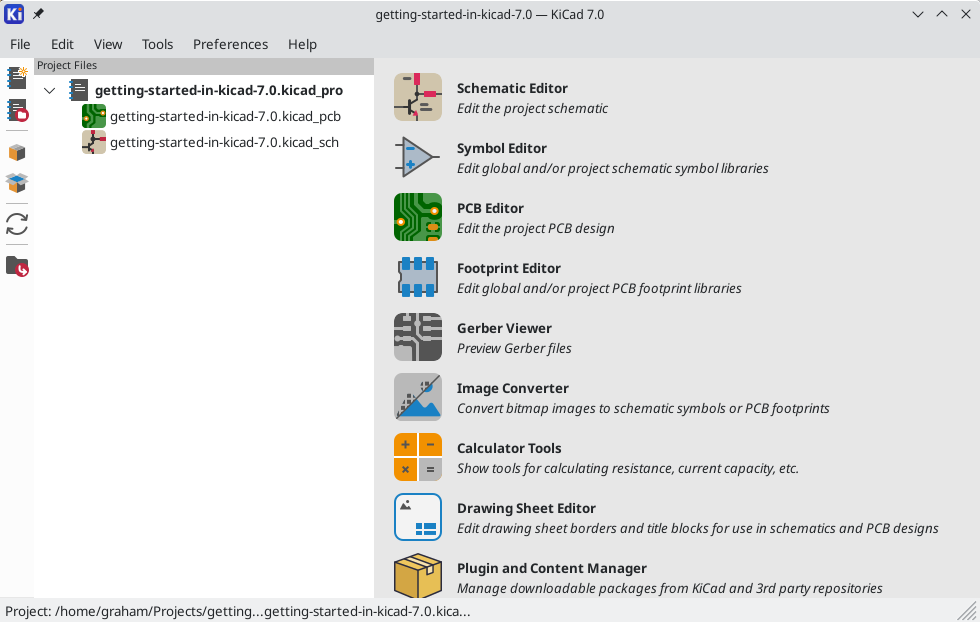
At left, the Project Files pane lists the files in the new project. There is a
project file with the extension .kicad_pro, a schematic file with the
extension .kicad_sch, and a board file with the extension .kicad_pcb. These
files all share a name with your project.
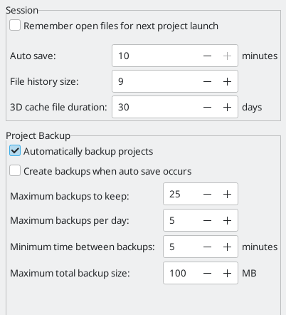
There may also be a -backups directory: KiCad will automatically create
backups of your project when you save, and optionally at fixed time intervals.
The backup settings are configurable by going to Preferences →
Preferences → Common → Project Backup.
At right of the Project Window, there are buttons to launch the various tools that KiCad provides. Launching these tools will automatically open the associated design file (schematic or PCB) from the current project. Start by opening the Schematic Editor.
Tutorial Part 2: Schematic
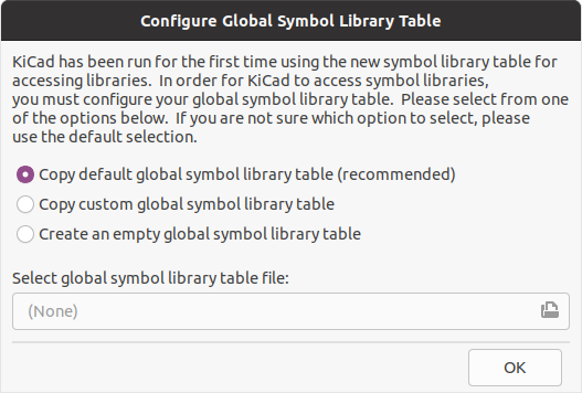
Symbol Library Table Setup
The first time the schematic editor is opened, a dialog will appear asking how to configure the global symbol library table. The symbol library table tells KiCad which symbol libraries to use and where they are located. If you have installed the default libraries with KiCad, which is recommended, select the default option: Copy default global symbol library table (recommended).
If KiCad cannot find the libraries in their expected installation location, this
option will be disabled. In this case, the user should choose the second
option, Copy custom global symbol library table. Click the folder button at
the bottom, and browse to the location given below. Select the sym-lib-table
file.
The location of the default library table files depends on operating system and may vary based on installation location. Below are the defaults for each operating system:
-
Windows:
C:\Program Files\KiCad\7.0\share\kicad\template\ -
Linux:
/usr/share/kicad/template/ -
macOS:
/Applications/KiCad/KiCad.app/Contents/SharedSupport/template/
Schematic Editor Basics
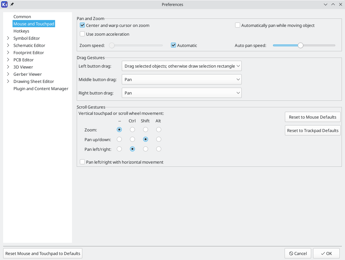
To pan around the schematic, click and drag with the middle mouse button or right mouse button. Zoom in and out with the mousewheel or F1 and F2. Laptop users may find it useful to change the mouse controls to be better suited to a touchpad; the mouse controls are configurable in Preferences → Preferences… → Mouse and Touchpad.
By default, KiCad enables a mouse setting called Center and Warp Cursor on Zoom. When this feature is enabled, the mouse cursor is automatically moved to the center of the screen when the user zooms in or out. This keeps the zoomed region centered at all times. This feature is unusual, but many users find it useful once they get used to it. Try zooming in and out with the mouse cursor in different areas of the canvas. If the default zoom behavior is uncomfortable, disable the feature in the Mouse and Touchpad preferences.
The toolbar at the left side of the screen contains basic display settings. The toolbar at the right side of the screen contains tools for editing the schematic.
Most tools in KiCad either have default hotkeys assigned, or can have custom hotkeys assigned. To view all hotkeys, go to Help → List Hotkeys…. Hotkeys can be changed in Preferences → Preferences… → Hotkeys.
Schematic Sheet Setup
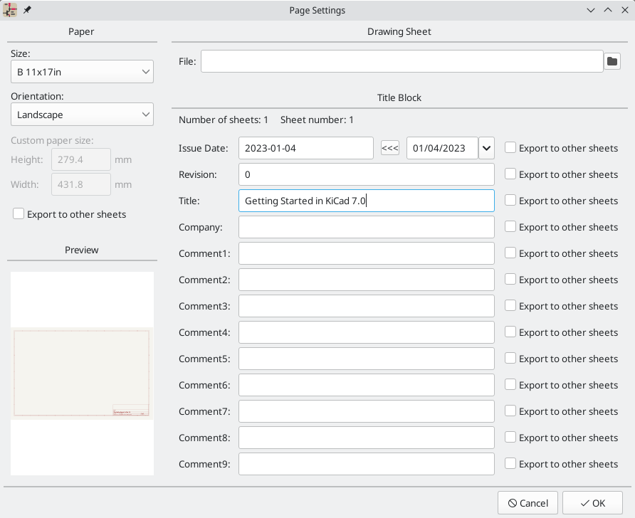
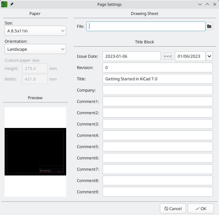
Before drawing anything in the schematic, set up the schematic sheet itself. Click File → Page Settings. Give the schematic a title and date, and change the paper size if desired.
Adding Symbols to the Schematic
Start making the circuit by adding some symbols to the schematic. Open the
Choose Symbol dialog by clicking the Add a Symbol button
 on the right side of the window or
pressing A.
on the right side of the window or
pressing A.
This action will trigger the Footprint Library Table Setup dialog. This dialog is equivalent to the Symbol Library Table Setup dialog explained earlier, but for footprints instead of symbols.
Again, select the default option: Copy default global footprint library table
(recommended). If this is option is disabled, select the second option, Copy
custom global footprint library table. Click the folder button at the bottom,
and browse to the location given in
the symbol library table setup instructions.
Select the fp-lib-table file and click OK.
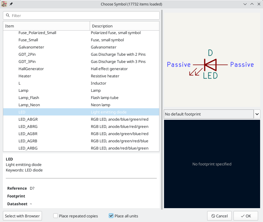
The Choose Symbol dialog lists the available symbol libraries and the component
symbols contained within them. Basic devices like passive components, diodes,
and other generic symbols are found in the Device library. Specific devices,
such as a particular LED, may be found in other libraries.
Scroll down to the Device library, expand it, and select the LED symbol.
Click OK, and click again to place the symbol in the schematic.
Next, add a current-limiting resistor. Go back to the symbol chooser, but this
time try searching for a resistor by entering R in the filter box at the top.
Again, it is found in the Device library. The R device is an IEC-style
rectangular resistor symbol. An R_US symbol is also available for users who
prefer the ANSI-style zigzag symbol. Select a resistor symbol and add it to the
schematic.
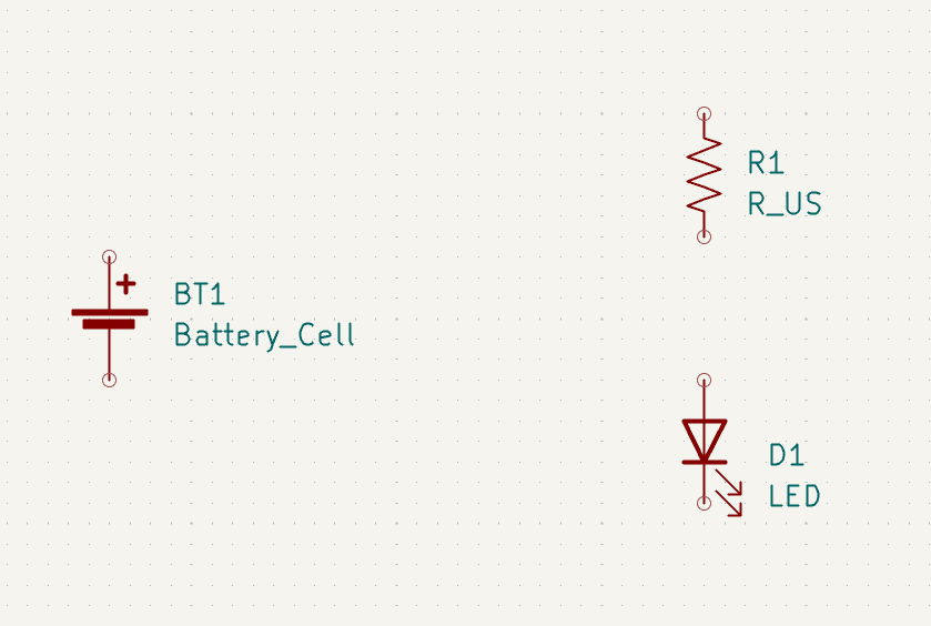
Finally, add a battery to power the LED. The Device library has a suitable
Battery_Cell symbol.

Selecting and Moving Objects
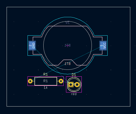
Next, position the symbols correctly relative to each other, as shown in the screenshot. Do this by selecting, moving, and rotating the symbols.
In KiCad 7.0, objects are selected by clicking on them. Additional objects can be added to the selection with Shift+click, or removed with Ctrl+Shift+click (macOS: Cmd+Shift+click). You can toggle an item’s selection state with Ctrl+click (macOS: Cmd+click).
Drag selection is also possible; dragging from left-to-right selects objects that are entirely enclosed by the selection box, while dragging right-to-left also selects objects that are partially enclosed by the selection box. Shift, Ctrl+Shift (Cmd+Shift), and Ctrl (Cmd) can also be used with drag selection to add, subtract, or toggle from the selection, respectively.
Note that it is possible to select an entire symbol (by clicking on the symbol shape itself) or to select one text field in the symbol without selecting the rest of the symbol (by clicking the text). When just a text field is selected, any actions performed will act only on the selected text and not on the rest of the symbol.
Selected objects are moved by pressing M and rotated by pressing R. The G hotkey (drag) can also be used to move objects. For moving unconnected symbols, G and M behave identically, but for symbols with wires attached, G moves the symbol and keeps the wires attached, while M moves the symbol and leaves the wires behind. Selected objects can be deleted with the Del key.
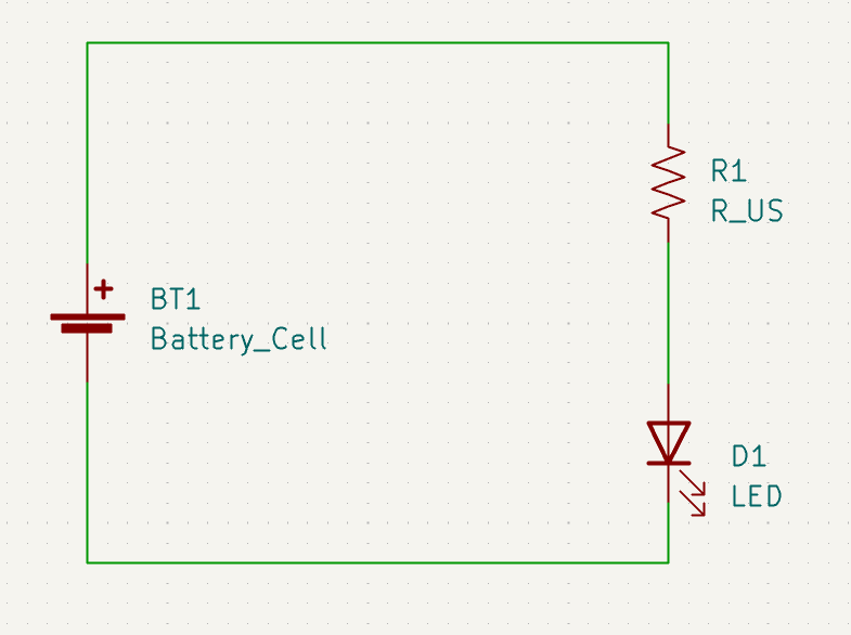
Wiring the Schematic
The symbol pins all have small circles on them, indicating that they are not
connected. Fix that by drawing wires between symbol pins as shown in the
screenshot. Click the Add a Wire button
 on the right-hand toolbar or use the
W hotkey. Click to start drawing a wire, and finish drawing the wire by
clicking on a symbol pin or double clicking anywhere. Pressing Escape will
cancel drawing the wire.
on the right-hand toolbar or use the
W hotkey. Click to start drawing a wire, and finish drawing the wire by
clicking on a symbol pin or double clicking anywhere. Pressing Escape will
cancel drawing the wire.
Another convenient method of drawing wires is to hover over an unconnected pin. The mouse cursor will change to indicate that a wire can be drawn starting from that location. Clicking on the pin will then begin drawing a wire automatically.
Next, add power and ground symbols to the schematic. While not strictly necessary in such a simple schematic, these make it easier to understand large schematics.
A number of power and ground symbols are available in the Power symbol library.
However, there is a shortcut for adding these symbols: click the Add a Power
Symbol button  or use the P hotkey. This
brings up the Choose a Symbol dialog, but only displays symbol libraries
that contain power symbols.
or use the P hotkey. This
brings up the Choose a Symbol dialog, but only displays symbol libraries
that contain power symbols.
Add a VCC symbol and GND symbol and then connect them to the circuit with wires.
Finally, add a label to the wire between the LED and resistor. Again, this may not
be necessary in a simple circuit, but it is good practice to label important nets.
Click the Net Label button  in the right
toolbar (L), type a label name (
in the right
toolbar (L), type a label name (led), and place the label into the
schematic so that the square attachment point overlaps with the wire. Rotate and
align the label as necessary.
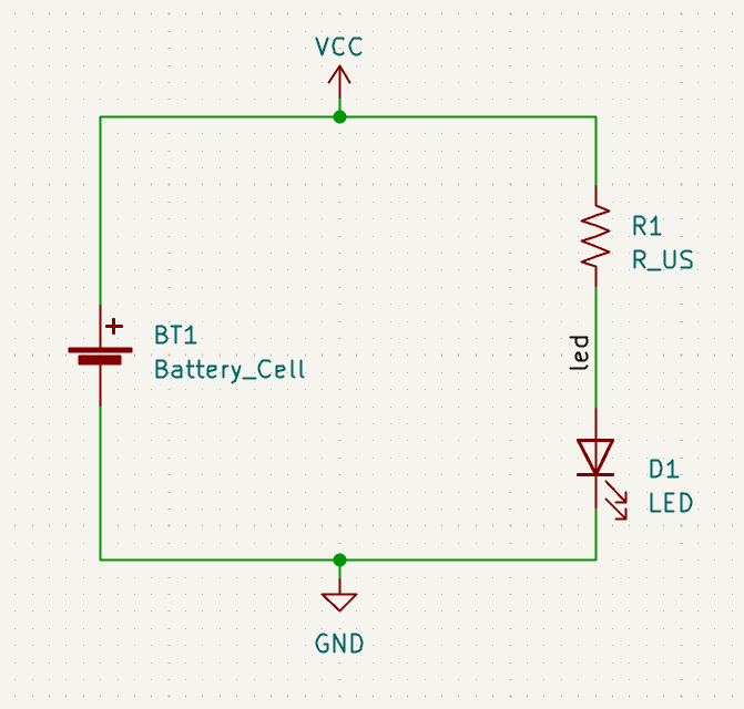
Note that labels and power symbols with the same name are connected together.
Another GND symbol or wire labeled led on this schematic page would be shorted
to the existing one, even without wires visually connecting them.
Annotation, Symbol Properties, and Footprints
Annotation
Each symbol needs a unique reference designator assigned to it. This process is also known as annotation.
By default in KiCad 7.0, symbols are automatically annotated when they are added
to the schematic. Automatic annotation can be enabled or disabled using the
 button in the left toolbar.
While it is not necessary for this guide, symbols can be manually annotated or
reannotated using the Fill in schematic symbol reference designators button
() in the top toolbar.
Symbol Properties
Next, fill in values for each component. Select the LED, right-click, and select
Properties… (E). This project will use a red LED, so change the Value
field to be red. In a real project, it might be better to write the LED
manufacturer’s part number here instead. Note that it’s possible to edit
reference designators individually in each symbol’s properties.
This project will use a 3V lithium coin cell battery, so change the Value
field of BT1 to 3V. Change the resistor’s value to 1k.
Footprint Assignment
Finally, assign a footprint to each component. This defines how each component will attach to the PCB. Some symbols come with footprints pre-assigned, but for many components there are multiple possible footprints, so the user needs to select the appropriate one.
There are several ways to assign footprints, but one convenient way is to use
the footprint assignment tool by clicking the
![]() button in the top toolbar.
button in the top toolbar.
The left pane of this window lists the available footprint libraries. The middle pane shows the symbols in the schematic. All of these symbols will get footprints assigned to them. The right pane shows the footprints that can be chosen for the symbol selected in the middle pane. To assign a footprint to a symbol, select the symbol in the middle pane and double click on the desired footprint in the right pane. You can preview a footprint by right-clicking the footprint’s name and selecting View selected footprint.
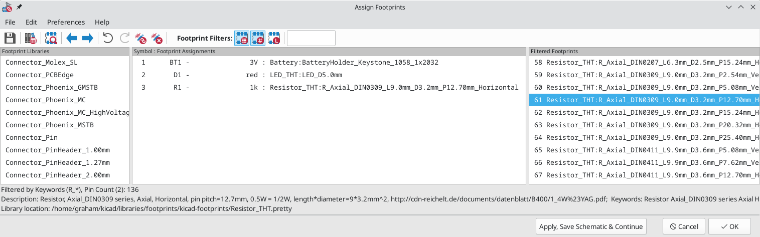
Many footprints are included with KiCad, so the footprint assignment tool offers several ways to filter out footprints that aren’t relevant to the symbol in question.

-
The leftmost button
 activates filters that can be
defined in each symbol. For example, an opamp symbol might define filters
that show only SOIC and DIP footprints. Sometimes those predefined filters
are missing or too restrictive, so it can be useful to turn this filter off
in some situations.
activates filters that can be
defined in each symbol. For example, an opamp symbol might define filters
that show only SOIC and DIP footprints. Sometimes those predefined filters
are missing or too restrictive, so it can be useful to turn this filter off
in some situations. -
The middle button
 filters by
pin count, so that only 8-pad footprints are shown for 8-pin symbols. This
filter is almost always useful.
filters by
pin count, so that only 8-pad footprints are shown for 8-pin symbols. This
filter is almost always useful. -
The right button
 filters by selected
library. Libraries are selected in the left pane; footprints not in the
selected library will be filtered out. This filter is useful as long as it is
known which library contains the right footprint. Often it’s best to use this
filter or the symbol filters, but not both.
filters by selected
library. Libraries are selected in the left pane; footprints not in the
selected library will be filtered out. This filter is useful as long as it is
known which library contains the right footprint. Often it’s best to use this
filter or the symbol filters, but not both. -
The text box filters out footprints that don’t match the text in the box. This filter is disabled when the box is empty.
Using the filters, find each of the footprints shown in the central column in the screenshot above. Assign each footprint to a symbol by selecting the symbol in the central column and then double clicking the appropriate footprint in the right column. Once all of the footprints have been assigned, click OK.
There are other ways to assign footprints; one way is through the symbol properties window. For more information on assigning footprints, see the manual.
Electrical Rules Check
The last remaining thing to do in the schematic is to check for electrical errors. KiCad’s Electrical Rules Checker (ERC) cannot make sure that the design in the schematic will work, but it can check for some common connection issues such as unconnected pins, two power outputs shorted together, or a power input that isn’t powered by anything. It also checks for some other mistakes like symbols that aren’t annotated and typos in net labels. To see the full list of electrical rules and to adjust their severity, go to File → Schematic Setup… → Electrical Rules → Violation Severity. It is a good idea to run ERC before starting layout.
Run an electrical rules check by clicking the ERC button
( ) in the top toolbar and then clicking Run ERC.
Even in this simple schematic, KiCad has found two potential errors. The errors are listed in the ERC window, and arrows point to the violation locations in the schematic. Selecting a violation in the ERC window highlights the corresponding arrow.
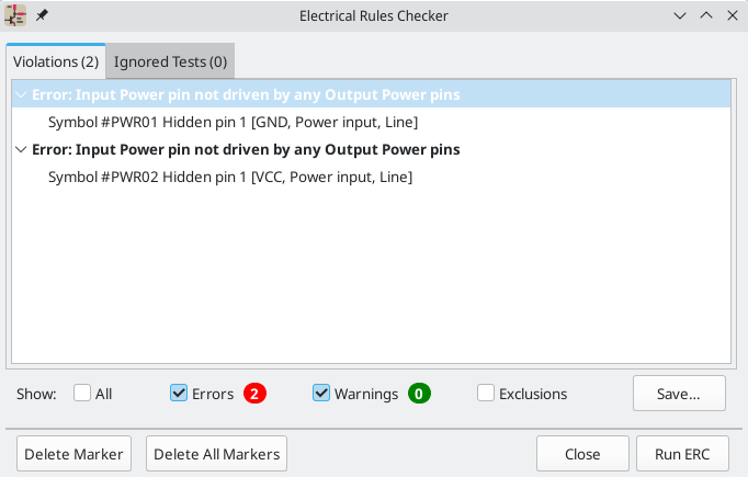
You can exclude individual violations or ignore entire classes of violations by right clicking on each error message. However, it’s usually worth addressing the violations, even if they aren’t actual design errors, in order to get a clean ERC report and avoid missing real problems.
In this case, KiCad reports "Input Power pin not driven by any Output Power
pins" for both the VCC and GND nets. This is a common KiCad ERC error.
Power symbols are set up to require a power output pin, such as the output of a
voltage regulator, on the same net; otherwise KiCad thinks the net is undriven.
To a human, it is obvious that VCC and GND are driven by the battery, but
it’s necessary to explicitly show that in the schematic.
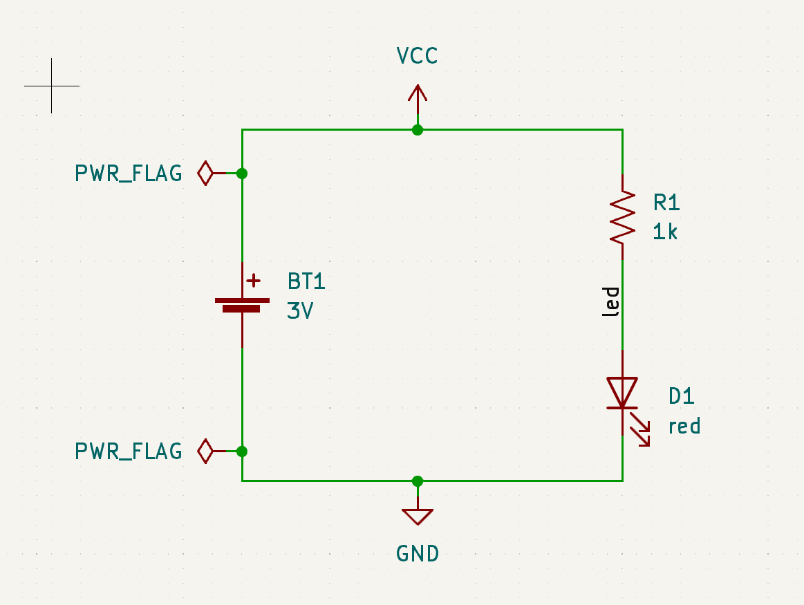
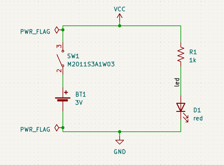
There is a special PWR_FLAG symbol in the Power symbol library that is used
to solve this problem by telling KiCad that the nets are actually driven. Add this
symbol to the VCC and GND nets and re-run ERC. When ERC passes without any
violations, the schematic is complete.
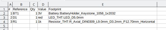
Bill of Materials
A final optional step is to generate a Bill of Materials listing all components used in the project. Click Tools → Generate BOM….
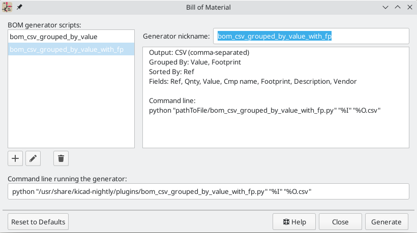
KiCad 7.0 uses Python scripts to generate BOMs. Three BOM scripts are included, and users can also create their own scripts to generate BOMs in whatever format is desired.
Select the bom_csv_grouped_extra script, and click generate. A CSV file
containing BOM information is created in the project directory. The BOM
generator also generates an intermediate XML file, which can be safely deleted.
Tutorial Part 3: Circuit Board
With the schematic completed, go back to the Project Window and open the PCB Editor, either by clicking the PCB Editor button or opening the board file.
PCB Editor Basics
Navigation in the PCB Editor is the same as the Schematic editor: pan by dragging with the middle mouse button or right mouse button, and zoom with the scrollwheel or F1/F2.
The main part of the PCB Editor is a canvas where the board will be designed. The toolbar on the left side has various display options for the board, including units and toggles for outline/filled display modes for tracks, vias, pads, and zones. The toolbar just to the right of the canvas contains tools for designing the PCB.
Some buttons on the right toolbar have a small triangle in the bottom
right corner  . The triangle
indicates that the button has an expanding palette containing several
related tools, for example different kinds of dimensions. To select an
alternate tool, click and hold on the button until the palette appears,
then click on the alternate tool. Another way to use the palettes is to
click on the button and drag to the left until the palette appears, then
release the mouse button when the desired tool is highlighted. . The triangle
indicates that the button has an expanding palette containing several
related tools, for example different kinds of dimensions. To select an
alternate tool, click and hold on the button until the palette appears,
then click on the alternate tool. Another way to use the palettes is to
click on the button and drag to the left until the palette appears, then
release the mouse button when the desired tool is highlighted.
|
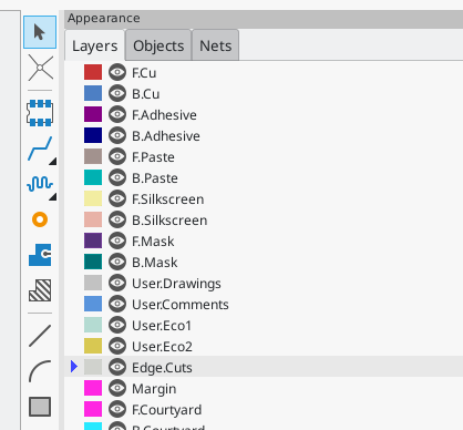
At far right is the Appearance Panel and Selection Filter. The Appearance panel is used to change visibility, colors, and opacity of PCB layers, objects, and nets. The active layer is changed by clicking on the name of a layer.
Below the Appearance Panel is the Selection Filter, which enables and disables selection of various types of PCB objects. This is useful to select specific items in a crowded layout.
Board Setup and Stackup
Before designing the board, set the page size and add information to the title block. Click File → Page Settings…, then choose an appropriate paper size and enter a date, revision, and title.
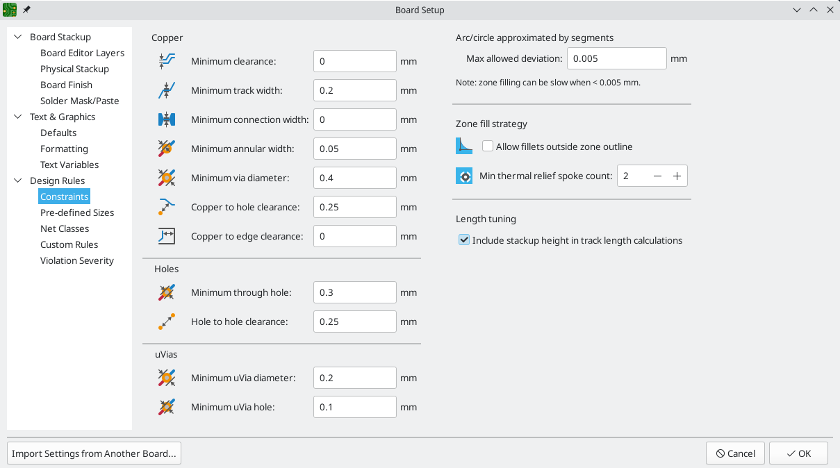
Next, go to File → Board Setup… to define how the PCB will be manufactured. The most important settings are the stackup, i.e. what copper and dielectric layers the PCB will have (and their thicknesses), and the design rules, e.g. sizes and spacing for tracks and vias.
To set the stackup, open the Board Stackup → Physical Stackup page of the Board Setup window. For this guide, leave the number of copper layers at 2, but more complicated projects might require more layers.
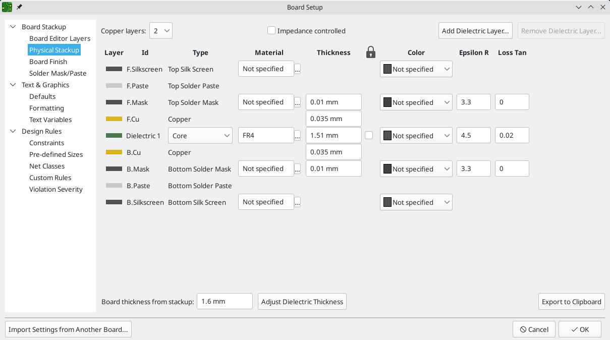
Next, go to the Design Rules → Constraints page. The settings on this page specify the overriding design rules for everything in the board design. For the purposes of this guide, the defaults are fine. However, for a real project these should be set according to the capabilities of the PCB fab house so that the PCB design is manufacturable.
Finally, open the Design Rules → Net Classes page. A net class is a set of design rules associated with a specific group of nets. This page lists the design rules for each net class in the design and allows assigning nets to each net class.
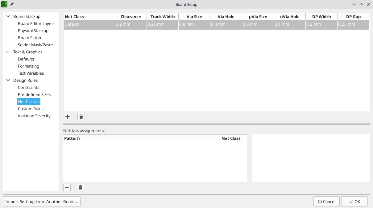
Track width and spacing can be managed manually by the designer during layout, but net classes are recommended because they provide an automatic way to manage and check design rules.
In this design, no net classes are specified, so all nets will belong to the
Default net class. The default design rules for this net class are
acceptable for this project, but other designs may have multiple net classes,
each with different design rules. For example a board might have a High
Current netclass with wide traces, or a 50 ohm netclass with specific width
and clearance rules for 50 ohm controlled-impedance traces.
Importing Changes From Schematic
The schematic is complete, but there are not yet any components in the layout.
To import design data from the schematic into the layout, click Tools →
Update PCB from Schematic…, or press F8. There is also a button
 in the top toolbar.
Read through the messages in the Changes To Be Applied window, which will say that the three components in the schematic will be added to the board. Click Update PCB, Close, and click on the canvas to place the three footprints. The location of each footprint relative to the others will be changed later.
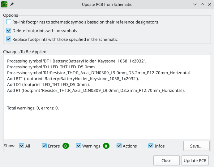
In KiCad, updating the PCB with changes in the schematic is a manual process: the designer decides when it is appropriate to update the PCB with modifications in the schematic. Each time the schematic is edited, the designer must use the Update PCB from Schematic tool to keep the schematic and layout in sync.
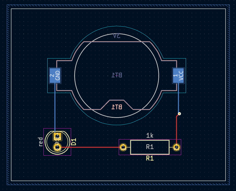
Drawing A Board Outline
Now the three components have been placed, but the board itself has not been
defined. The board is defined by drawing a board outline on the Edge.Cuts
layer.
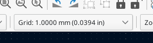
It’s often useful to draw the board outline with a coarse grid, which makes it easy to get round numbers for the board size. Switch to a coarse grid by selecting 1mm in the Grid dropdown menu above the canvas.
To draw on the Edge.Cuts layer, click Edge.Cuts in the Layers tab of the
Appearance panel at right. Choose the rectangle tool
 in the right toolbar, click on the canvas to
place the first corner, then click again to place the opposite corner so that
the rectangle roughly surrounds the three footprints. The other graphic tools
(line , arc
in the right toolbar, click on the canvas to
place the first corner, then click again to place the opposite corner so that
the rectangle roughly surrounds the three footprints. The other graphic tools
(line , arc  , circle
 , polygon
 , or a combination of them) could
also be used to define the board outline; the only requirement is that the
outline is a single closed shape that doesn’t intersect itself.
, or a combination of them) could
also be used to define the board outline; the only requirement is that the
outline is a single closed shape that doesn’t intersect itself.
Placing Footprints
The next step in the layout process is to arrange the footprints on the board. In general, there are a several considerations for positioning footprints:
-
Some footprints may have exact requirements for their locations, such as connectors, indicators, or buttons and switches.
-
Some components may need to be placed according to electrical considerations. Bypass capacitors should be close to the power pins of the associated IC and sensitive analog components should be far from digital interference.
-
Almost all components have a "Courtyard" (or two if both Front and Back are defined). Generally Courtyards should not intersect.
-
Otherwise components should be positioned for ease of routing. Connected components should generally be close together, and arranged to minimize routing complexity. The ratsnest (the thin lines indicating connections between pads) is useful for determining how best position footprints relative to other footprints.
For the purposes of this guide, the only placement goal is to make the routing process as simple as possible.
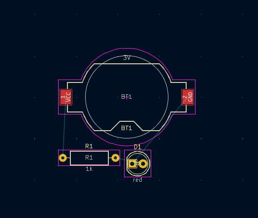
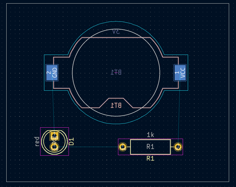
Start by moving the battery holder BT1 onto the back side of the board. Click
it to select it, then press M to move it. Press F to flip it to the
opposite side; it now appears mirrored and its pads have changed from red to
blue.
All PCB layers are viewed from front side of the board. Footprints on the bottom of the board are therefore upside down and appear mirrored.
Each PCB layer has a unique color, which is shown by the swatches in the Layers
tab of the Appearance panel. In the default color scheme, items on the F.Cu
(Front Copper) layer are red, while items on the B.Cu (Back Copper) are blue.
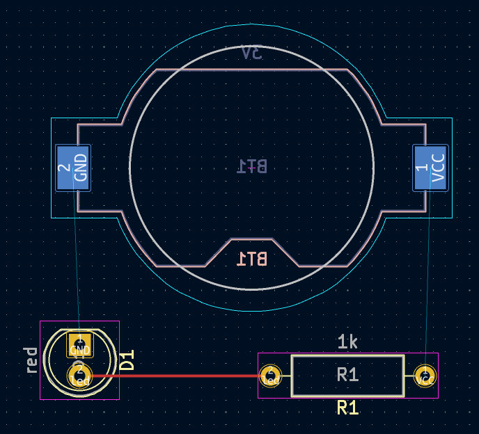
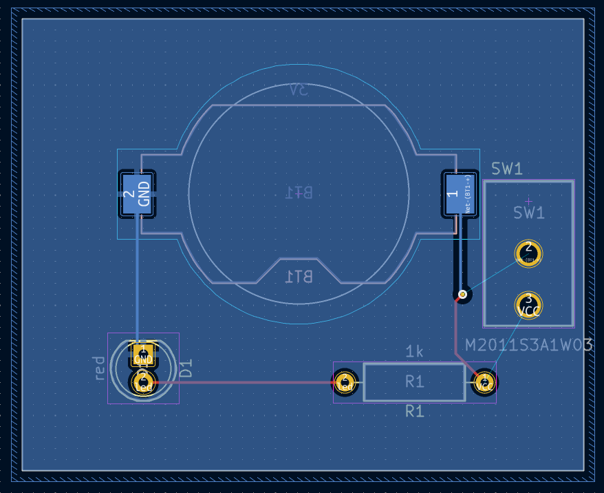
Now place the other two components. One at a time, select each component, then move and rotate it with M and R. Watch the ratsnest lines between each pad to choose the simplest arrangement of components; a good arrangement will leave the lines untangled. One possible arrangement is shown in the screenshot below.
Routing Tracks
With the components in place, it’s time to connect the pads with copper traces.
The first trace will be drawn on the front of the board, so change the active
layer to F.Cu in the Layers tab of the Appearance panel.
Click Route Tracks  in the right-hand
toolbar or press X. Click on the
in the right-hand
toolbar or press X. Click on the led pad of D1. The ratsnest line
indicates there is an unrouted connection to the led pad of R1, so click on
that pad to draw a trace connecting the two pads. Clicking on the second pad
completes the trace. The ratsnest line between the led pins is no longer drawn
because the connection has been made in copper.
Now draw a trace between the GND pads of BT1 and D1, starting with the BT1
pad on the back of the board. Notice that the active layer automatically changed
to B.Cu after clicking on the BT1 pad. Click on the D1 pad to finish the
track.
While BT1 has surface mount pads that are only on the bottom of the board,
D1 has through hole pads that can connect to tracks on both the front and
back. Through hole pads are one way to make a connection between multiple
layers. In this case, D1 is a component on the front side of the board, but
its through hole pads are used to connect to a trace on the back of the board.
Another way to make a connection across layers is with a via. Start routing at the
VCC pad of BT1 on the back of the board. Press V and click halfway
between BT1 and R1 to insert a via, which also switches the active layer to
F.Cu. Complete the track on the top side of the board by clicking on the
VCC pad of R1.
At this point, all connections are routed. This can be confirmed by looking at the status screen in the bottom left of the window, where the number of unrouted nets is given as 0.
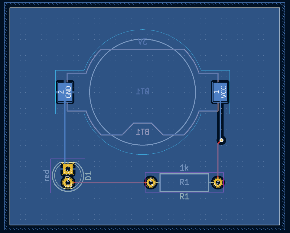
Placing Copper Zones
Copper zones are often used for ground and power connections because they provide a lower impedance connection than traces.
Add a GND zone on the bottom of the board by switching to the bottom copper
layer and clicking the Add a filled zone button
 in the right toolbar. Click on the PCB to place
the first corner of the zone.
in the right toolbar. Click on the PCB to place
the first corner of the zone.
In the Copper Zone Properties dialog that appears, select the GND net and make
sure that the B.Cu layer is selected. Click OK, then click to place the other
three corners of the zone. Double click when placing the last corner to complete
the zone.
The zone outline is displayed on the canvas, but the zone is not yet filled — there is no copper in the zone area, and therefore the zone is not making any
electrical connections. Fill the zone with Edit → Fill All Zones
(B). Copper has been added to the zone, but it doesn’t connect to the
VCC or led pads and traces, and is clipped by the board edge. It overlaps
with the GND trace drawn earlier, and it connects to the GND pads through
thin traces. These are thermal reliefs, which make the pads easier to solder.
Thermal reliefs and other zone settings can be modified in the zone properties
dialog.
In KiCad, zones are not filled automatically when they are first drawn or modified, or when footprints within them are moved. Zones are refilled by manually filling them and when running DRC. Make sure zone fills are up-to-date before generating fabrication outputs.
Sometimes filled zones can make it hard to see other objects in a crowded board
design. Zones can be hidden except for their boundaries using the Show only
zone boundaries button  on the
left-hand toolbar. Zones retain their filled status when only their outlines are
shown — hiding a zone fill is not the same as unfilling it.
on the
left-hand toolbar. Zones retain their filled status when only their outlines are
shown — hiding a zone fill is not the same as unfilling it.
Zones can also be made transparent using the Appearance panel, and inactive layers can also be hidden or dimmed using the Layer Display Options in the Appearance Panel.
Design Rule Checking
Design Rule Checking is the layout equivalent of Electrical Rule Checking for the schematic. DRC looks for design mistakes like mismatches between the schematic and layout, copper regions that have insufficient clearance or are shorted together, and traces that do not connect to anything. Custom rules can also be written in KiCad 7.0. To view the full list of design rules that are checked and to adjust their severity, go to File → Board Setup… → Design Rules → Violation Severity. Running DRC and fixing all errors is strongly advised before generating fabrication outputs.
Run a DRC check with Inspect → Design Rules Checker, or use the button
in the top toolbar. Click Run DRC. When the
checks are complete, no errors or warnings should be reported. Close the DRC
window.
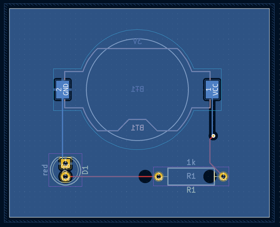
Now intentionally cause a DRC error by moving the resistor footprint to overlap
the filled area of the zone. Use D (Drag) to move the resistor footprint
slightly while keeping the traces attached to its pads. This creates a clearance
violation because the VCC and led pads of the resistor are shorted to the
GND zone fill. Ordinarily this would be fixed by refilling the zone, but don’t
refill the zone yet.
Run DRC again, but make sure to uncheck the Refill all zones before performing
DRC checkbox. DRC reports 6 violations: for each pad of R1, there is a
clearance violation between the pad and the zone, another clearance violation
between the pad’s through hole and the zone, and a third violation where the
pad’s solder mask opening exposes the copper of two different nets (the GND
fill and the trace connected to the pad). Arrows point to each violation in the
canvas. Clicking on each violation message zooms in on the respective
violation.
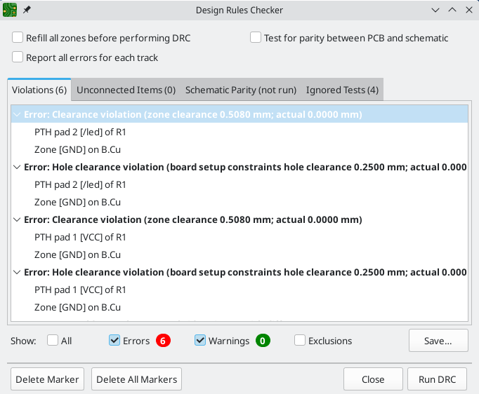
Close the DRC dialog, press B to refill the zone, and re-run DRC. Alternatively, check the Refill all zones before performing DRC checkbox and re-run DRC. All violations are fixed.
3D Viewer
KiCad offers a 3D viewer that is useful for inspecting the PCB. Open the 3D viewer with View → 3D Viewer. Pan by dragging with the middle mouse button, and orbit by dragging with the left mouse button. Orbit around the PCB to see the LED and resistor on the top, and the battery holder on the bottom.
A raytracing mode is available, which is slower but offers more accurate rendering. Switch to the raytracing mode with Preferences → Raytracing.
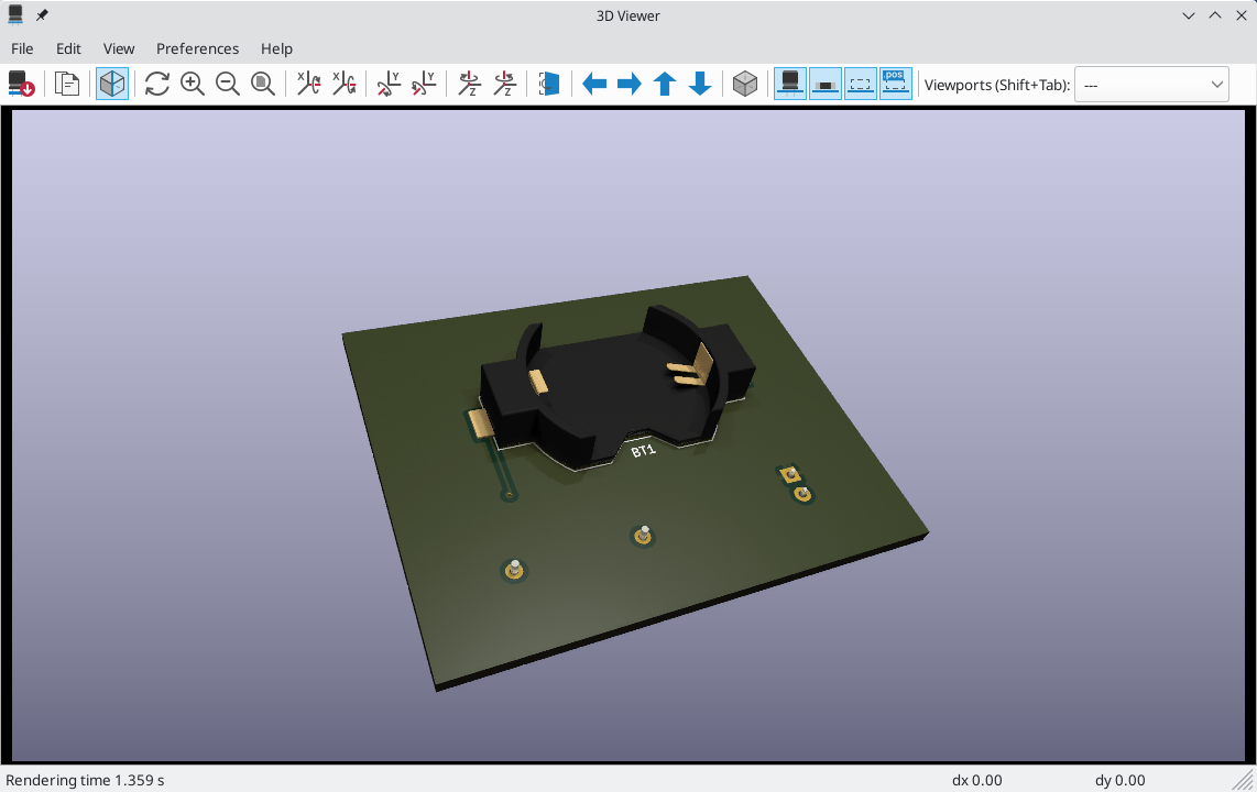
Many of the footprints in KiCad’s library come with 3D models, including all of the footprints used in this guide. Some footprints do not come with 3D models, but users can add their own.
Fabrication Outputs
With the board design finished, the final step is to generate fabrication outputs so the board can be manufactured.
Open the Plot dialog with File → Plot…. This dialog can plot the design in several formats, but Gerber is usually the right format for ordering from a PCB fabricator.
Specify an output directory so that the plotted files will be collected in a
folder. Otherwise, the default settings are fine, but make sure all the necessary
layers are checked: include the copper layers (*.Cu), board outline
(Edge.Cuts), soldermask (*.Mask), and silkscreen (*.Silkscreen).
The paste layers (*.Paste) are useful for manufacturing solder paste
stencils. The Adhesive layers (*.Adhesive) are needed only if any
components will be glued to the board during assembly. Other layers may be
useful to plot, but are not typically necessary for PCB fabrication.
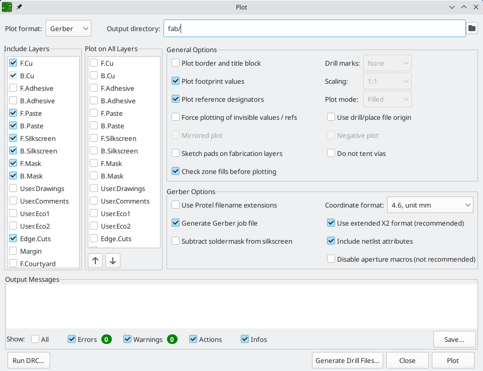
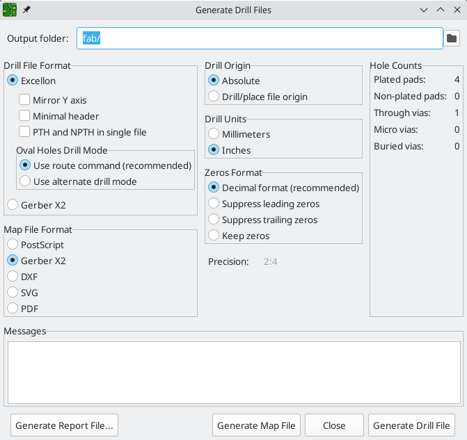
Click Plot to generate the Gerber files. Also click Generate Drill Files… and then Generate Drill File to create files specifying the location of all holes that will be drilled in the board. Finally, close the Plot dialog. The design is finished.
Tutorial Part 4: Custom Symbols and Footprints
The circuit would be improved by adding a switch to turn the LED on and off. The process to add this switch will require creating a new symbol and footprint library, drawing a switch symbol, and creating a footprint for the switch.
The specific switch that will be used in this guide is the NKK M2011S3A1W03, an SPST toggle switch. Many other switches could be used, but the pin numbering and footprint dimensions may need to be adjusted.
Library and Library Table Basics
Symbols and footprints are organized into libraries. A library can hold symbols or footprints, but not both.
KiCad keeps track of the user’s symbol libraries and footprint libraries in the symbol library table and footprint library table, respectively. Each library table is a list of library names and the location of where each library exists on disk.
In addition to global symbol and footprint library tables, there are also project library tables for symbols and footprints. Symbols and footprints that are added to the global tables are available in all projects, while symbols and footprints in the project-specific tables are available only for that specific project. Users can add their own libraries to the global library tables or to project-specific tables.
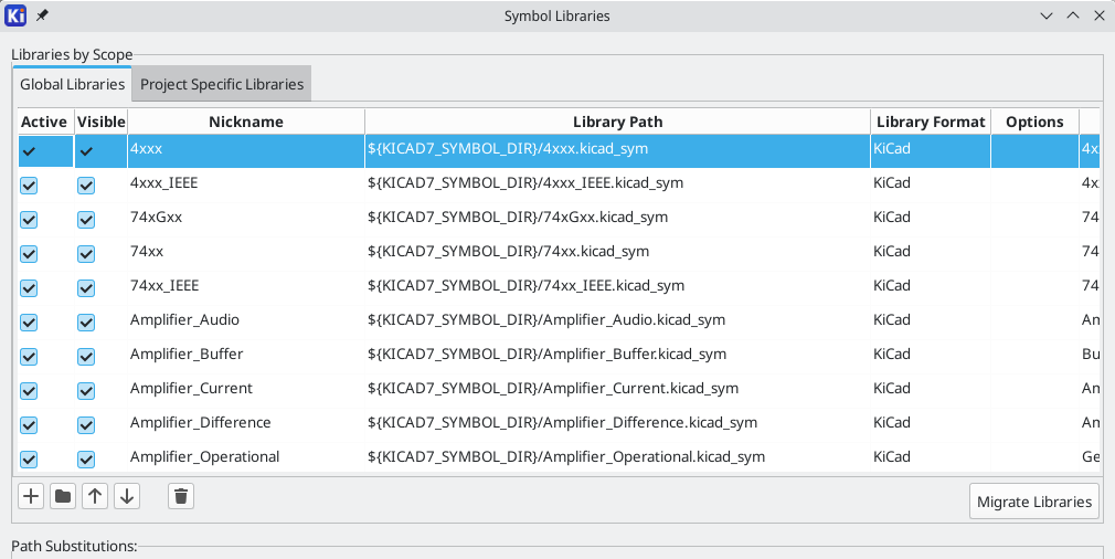
The symbol library tables can be viewed or edited with Preferences → Manage Symbol Libraries… in the Schematic Editor or Symbol Editor windows. The footprint library tables can be viewed or edited with Preferences → Manage Footprint Libraries… in the Board Editor or Footprint Editor. Both library tables can also be accessed from the Project Manager.
Often, paths to libraries are defined with path substitution variables. This enables a user to move all of their libraries to a new location without modifying the library tables. The only thing that needs to change is to redefine the variable to point to the new location. KiCad’s path substitution variables are edited with Preferences → Configure Paths… in the Project Manager or any of the Editor windows.
One useful path substitution variable is ${KIPRJMOD}. This variable always
points at the current project directory, so it can be used for including
project-specific libraries that are stored inside the project directory.
On first run, KiCad prompts the user to set up the symbol library table and footprint library table. To go through this setup again, delete or rename the symbol library table or footprint library table files. Make a backup of the tables before deleting them.
The location of the symbol and footprint library table files depends on operating system.
-
Windows:
%APPDATA%\kicad\7.0\sym-lib-tableand%APPDATA%\kicad\7.0\fp-lib-table -
Linux:
~/.config/kicad/7.0/sym-lib-tableand~/.config/kicad/7.0/fp-lib-table -
macOS:
~/Library/Preferences/kicad/7.0/sym-lib-tableand~/Library/Preferences/kicad/7.0/fp-lib-table
Creating New Global or Project Libraries
The first step in drawing a new symbol or footprint is to choose a library in which to store it. For this guide, the switch symbol and footprint will go into new project-specific libraries.
Open the Symbol Editor from the Project Manager. Click File → New
Library, and select Project. Choose a name for the new library (e.g.
getting-started.kicad_sym) and save it in the project directory. The empty new
library is now selected in the Libraries pane at left, and has been
automatically added to the project library table (check the Project Specific
Libraries tab in Preferences → Manage Symbol Libraries…).
Creating New Symbols
Now create the switch symbol in the new library. With the getting-started
library selected in the Libraries pane, click File → New Symbol…. In
the Symbol name field, enter the part number: M2011S3A1W03. Switch symbols
should have reference designators that start with SW, so change the Default
reference designator field to SW. All other fields can remain as the
defaults.
In the Libraries pane, the M2011S3A1W03 symbol now appears under the
getting-started library. In the canvas, a cross indicates the center of
the footprint, and text has been added for the symbol name and reference
designator. For now, move the text away from the center of the footprint to
get it out of the way.
Symbol Pins
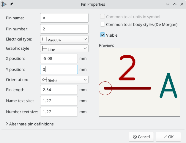
Start drawing the symbol by adding a pin. Click the Add a pin button
 on the right toolbar. The Pin Properties dialog will
appear. Set Pin name to
on the right toolbar. The Pin Properties dialog will
appear. Set Pin name to A, Pin number to 2, Electrical type to
Passive, and Orientation to Right. Set X Position to -5.08 mm and
Y Position to 0. Click OK, then click on the canvas to place the pin.
If the pin moved after clicking OK, it might be necessary to edit the pin’s
properties again (double click the pin, or right click on the pin →
Properties…) to set the position correctly.
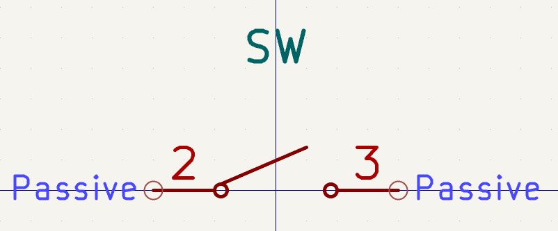
Add a second pin, but this time don’t use the Add a pin tool. Instead, press Insert. A new pin numbered 3 is added to the symbol, just below pin 2.
| In many places in KiCad, pressing Insert will repeat the last action. The location of the new item will be shifted and the numbering incremented automatically, as applicable. In the Symbol Editor, this can be used to place a large number of pins quickly. In the Schematic Editor, it can be used to repeatedly place a component, or to label a large component’s pins with numbered labels. Insert can be useful in the Footprint and Board Editors as well. |
We want Pin 3 to be on the right side of the switch symbol, so edit the
properties of pin 3 and change X position to 5.08, Y position to 0,
and Orientation to Left. Also, change Pin name to B.
Graphical Features
With the pins placed, use the circle and line
tools to make the symbol look like an SPST
switch. For this step, it will be useful to switch to a finer grid: right click
the canvas and select a smaller grid in the Grid submenu. After adding the
graphical shapes, switch back to a 50 mil grid.
| Small grids are useful for graphical features, but symbol pins must always be placed on a 50 mil (1.27 mm) grid. Pins which are not aligned to a 50 mil grid will not be able to connect to wires in the schematic. |
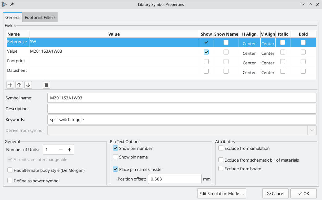
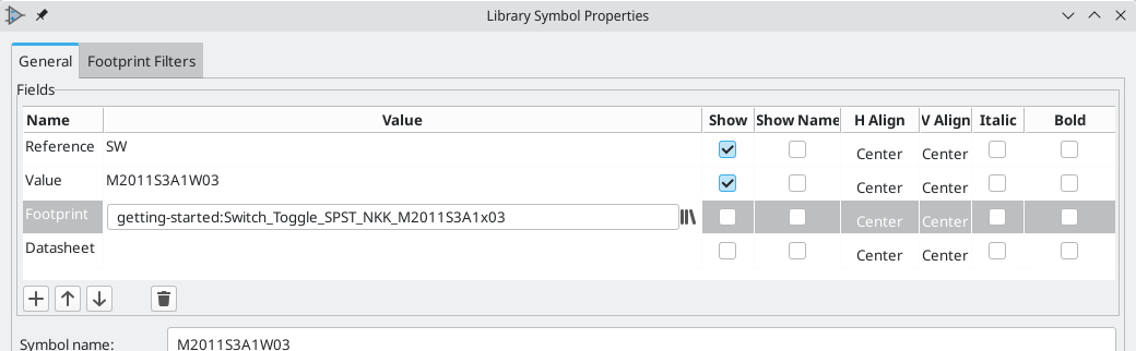
Symbol Properties
Now edit the properties for the whole symbol with File → Symbol
Properties, or by double clicking on the canvas. Change the Value field to
M2011S3A1W03, and add spst switch toggle to the Keyword field to make it
easier to find the symbol by searching. For this symbol, the pin names do not
add any useful information, so uncheck Show pin name to make the symbol
visually simpler.
After clicking OK, move the value field’s text lower so that it does not overlap with the symbol graphics.
The symbol is now complete. Save it and move on to creating a footprint.
Creating New Footprints
Open the Footprint Editor and create a new project-specific footprint library
named getting-started.pretty (File → New Library…). As with symbol
libraries, the new footprint library is added to the project library table. With
the new library selected in the Libraries pane, create a new footprint (File
→ New Footprint…). Set the name to Switch_Toggle_SPST_NKK_M2011S3A1x03
and the type to Through hole.
Footprint Pads
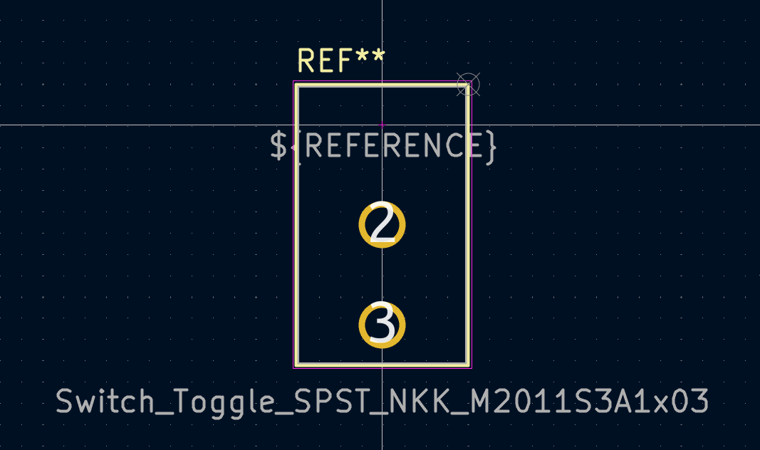
The switch has two pins, numbered in the datasheet as 2 and 3, and spaced 4.7 mm
apart. For ease of placement, adjust the grid to match the pad spacing. Click
View → Grid Properties… and change the User Defined Grid sizes to
4.7 mm. Accept the dialog, then switch to the user grid at the bottom of the
Grid: dropdown in the top toolbar.
By convention, through-hole footprints have pin 1 located at (0,0) and are oriented with pin 1 in the top left. The SPST version of this switch does not have pin 1, so the footprint will leave (0,0) empty and place pads 2 and 3 at (0, 4.7 mm) and (0, 9.4 mm). Note that in KiCad’s default coordinate system, the positive Y-axis is oriented downwards.
Use the Add a pad tool  in the right toolbar to
place a pad one grid division below the origin, which is (0, 4.7 mm). Press
Escape to exit the pad tool, then double click on the pad to edit its
properties. Change the pad number to
in the right toolbar to
place a pad one grid division below the origin, which is (0, 4.7 mm). Press
Escape to exit the pad tool, then double click on the pad to edit its
properties. Change the pad number to 2 and verify that the position is
correct. The switch pins are 1.17 mm x 0.8 mm, which gives a diagonal (maximum
pin dimension) of 1.42 mm. Therefore set the hole diameter to 1.42 mm + 0.2 mm =
1.62 mm, and the pad diameter to 1.62 mm + 2*0.15 mm = 1.92 mm to provide a
sufficient annular ring.
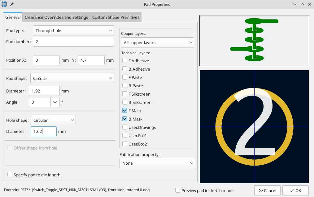
Now use the Add a pad tool again to place the other pad at (0, 9.4 mm). Notice that the pad number is automatically incremented and the properties including pad size and hole size are copied from the previous pad.
With both pads placed, the annular rings look slightly small. The switch will be
easier to solder and mechanically more robust if the annular rings are made
larger. Increase the annular ring thickness from 0.15 mm to 0.3 mm by editing
pad 2 and changing the pad size to 1.62 mm + 2*0.3 mm = 2.22 mm. Do not change
the hole size. Note that the pad size field accepts mathematical expressions, so
1.62+2*0.3 can be entered directly and will evaluate to 2.22 mm.
| Many text boxes in KiCad support mathematical expressions, including unit conversions. |
Make the same annular ring modification to the other pad as well. As a shortcut, right click on pad 2, click Push Pad Properties to Other Pads…, and then click Change Pads on Current Footprint.
Footprint Graphics
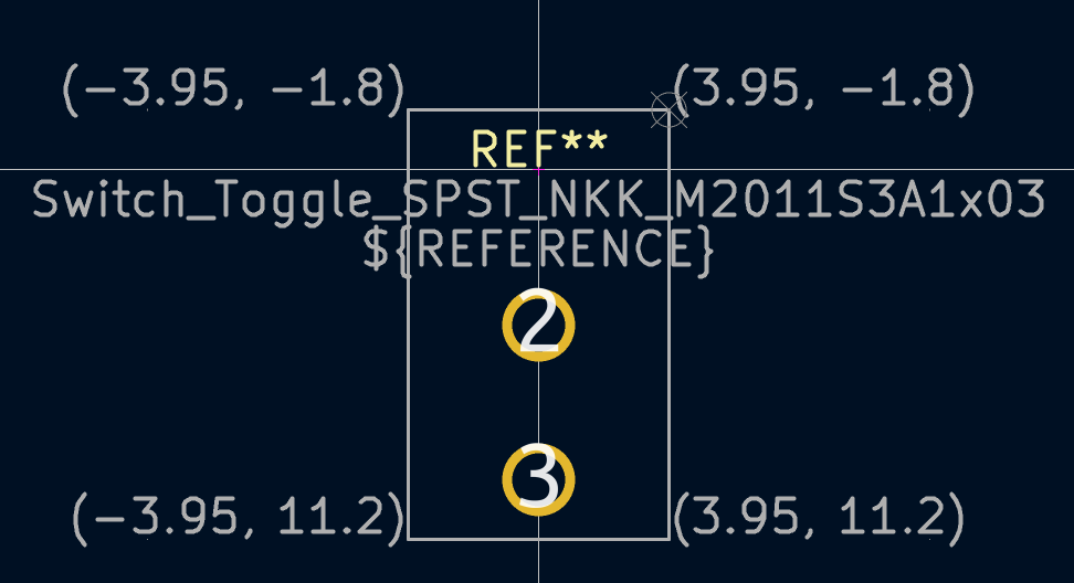
A good footprint will have the exact part outline drawn on the fabrication layer
(F.Fab), a slightly larger outline on the silkscreen layer (F.Silkscreen),
and a courtyard (F.Courtyard) surrounding the entire footprint to prevent
overlaps with other footprints.
Switch to the front fabrication layer by clicking F.Fab in the Layers panel
at right. The fabrication outline should precisely match the physical dimensions
of the part, which is 7.9 mm wide and 13 mm tall. Use the line
, rectangle ,
or polygon tools to draw the outline
of the part as shown in the screenshot below. One way to precisely place the
outline is to set the user grid as follows:
-
X grid:
7.9 mm -
Y grid:
13 mm -
X origin: 7.9 mm / 2 =
3.95 mm -
Y origin: 4.7 mm - (13 mm / 2) =
-1.8 mm
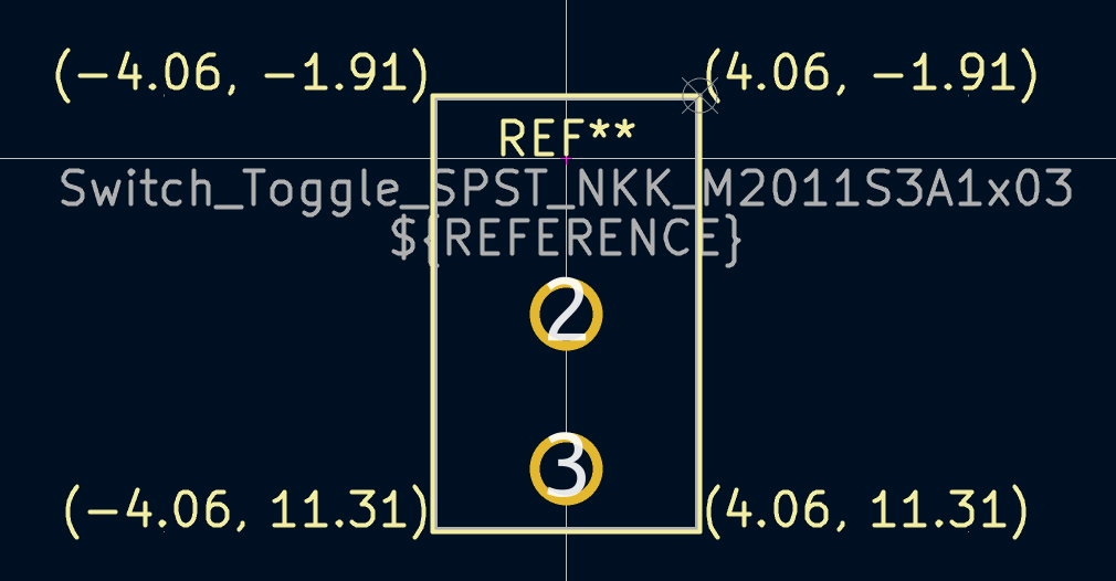
Next, switch to the F.Silkscreen layer. The silkscreen outline should be just
outside of the part outline, so the silkscreen lines are moved outwards from the
fabrication drawing by 0.11 mm (half of 0.10 mm fab line width, plus half of the
0.12 mm silkscreen line width). The exact coordinates are shown in the
screenshot below, and helpful grid settings are:
-
X grid: 7.9 mm + 2 * 0.11 mm =
8.12 mm -
Y grid: 13 mm + 2 * 0.11 mm =
13.22 mm -
X origin: 8.12 mm / 2 =
4.06 mm -
Y origin: -1.8 mm - 0.11 mm =
-1.91 mm
Finally, select the F.Courtyard layer. The courtyard outline should surround
the part with a 0.25 mm clearance.
Use a different strategy to draw this layer. Switch to a 1mm grid instead of the User grid, and draw a rectangle roughly surrounding the footprint. Double click on the rectangle to edit its properties, and enter the corner coordinates of the rectangle directly — they are shown in the screenshot below.
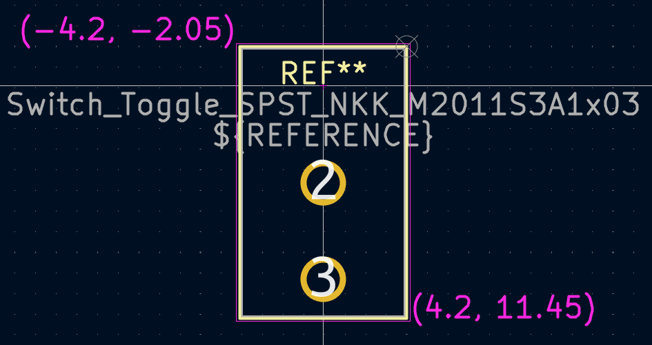
After completing the outlines, position the text as shown below. The footprint is complete.
Kicad Library Conventions
To maintain high-quality symbol and footprint libraries, KiCad has a KiCad Library Conventions document, which is a set of guidelines for symbols and footprints. It is not necessary to follow these conventions for personal libraries, but they are a good starting point. Footprints and symbols in the official library are required to follow KLC. KLC is used as a basis for the symbol and footprint in this guide.
Add Switch to Schematic
Now that the footprint is complete, the switch symbol can be modified so that the matching footprint is used for it by default.
Go back to the symbol editor and open the switch symbol. Edit the Symbol
Properties. Click in the Footprint field, then click the library book icon
 that appears. Browse to the project
footprint library and double click on the switch footprint. Save the symbol.
that appears. Browse to the project
footprint library and double click on the switch footprint. Save the symbol.
The switch footprint is now assigned to this symbol by default; the footprint does not need to be manually selected each time the symbol is added to a schematic.
Open the schematic, add a new symbol, and select the new switch symbol. Wire it to connect or disconnect the LED and the battery.
Reannotate the schematic to set the switch’s reference designator to SW1. It
isn’t necessary to manually choose a footprint for the switch, because the
switch symbol already specifies a footprint. Run ERC to make sure that the
modified schematic doesn’t violate any electrical rules.
Add Switch to Layout
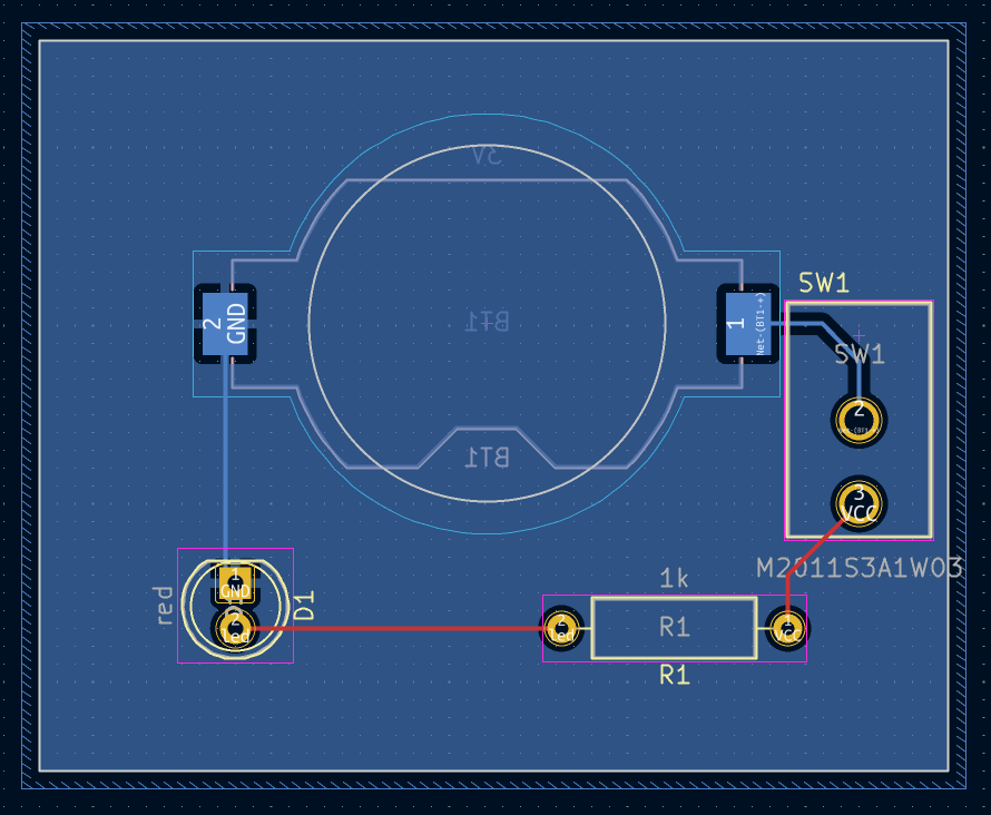
Make sure the schematic is saved, then open the Board Editor to add the symbol to the layout. Update the PCB with the schematic changes using Tools → Update PCB from Schematic… and place the switch footprint onto the board as shown.
The ratsnest shows the new connections that need to be routed. Additionally, the connection between the battery and the resistor needs to be deleted.
First, delete the unneeded traces. Select one of the traces between the battery and the resistor — it doesn’t matter which. Press U several times to expand the selection to include all the segments between the battery and resistor. Press Delete to remove the connection.
Route the new traces between the battery and the switch, and between the switch and the resistor. Press B to refill the zones.
Finally, re-run DRC to make sure the modified board doesn’t violate any design rules.
Linking Symbols, Footprints, and 3D Models
Symbols and Footprints
As described in the footprint assignment section, each
symbol in the schematic needs to have a footprint assigned to it during the
schematic entry process. The name of the footprint assigned to each symbol is
stored in the Footprint field of the symbol’s properties.
Symbols can specify a preselected footprint. Footprints do not need to be manually assigned to such symbols, because a footprint was chosen when the symbol was created. Users can override the preselected footprint during the footprint assignment process as normal. Defining a default footprint is a good idea for symbols that will usually or always have the same footprint assigned to it, for example a component which is only available in one package. The switch footprint was set as the default for its matching symbol.
Symbols can also specify footprint filters, which can be used to hide footprints
that are incompatible with the symbol. For example, the 74HC00 symbol has
footprint filters that result in only the applicable DIP and SO14 footprints being
displayed in the assign footprints tool.
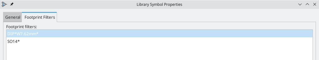
The KLC requirements for footprint filters contain some useful tips for effective footprint filters.
Footprints and 3D Models
3D models for components are stored in separate files. Filenames for the component’s 3D model(s) are saved in the footprint. Any number of 3D models can be added to each footprint. 3D model filenames, along with model scale, rotation, offset, and opacity, are set in the 3D Models tab of the Footprint Properties.
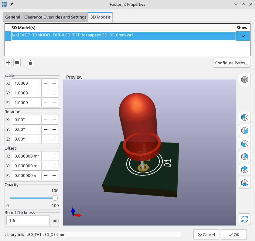
Both STEP (.step) and VRML (.wrl) 3D model formats are supported. STEP files
are useful where dimensional accuracy is needed, while VRML files can be used
for more visually attractive renders. Many footprints in KiCad’s library have
associated 3D models; these models are provided in both VRML and STEP formats.
Only one of the two models needs to be listed in the footprint (typically the
VRML filename is given). KiCad can automatically substitute the STEP version
when exporting a 3D model of the board for mechanical CAD purposes.
| Not all footprints in KiCad’s library are provided with 3D models, but all footprints list a 3D model filename even if the 3D model does not exist. This is so 3D models can be added at a later date without needing to edit the footprint. |
FreeCAD together with the StepUp Workbench are useful for creating component 3D models; they are used for many of the models in KiCad’s library. StepUp is used to generate STEP and VRML files with correct placement, scaling, and rotation.
Where To Go From Here
More Learning Resources
For more information on how to use KiCad, see the manual.
Other resources include the official KiCad user forum, Discord or IRC, and additional learning resources from the KiCad community.
To see more of what’s possible with KiCad, browse the Made With KiCad section of the website, or open the demo projects included with KiCad (File → Open Demo Project…).
Help Improve KiCad
To report a bug or request a feature, please use Help → Report a Bug or open an issue on Gitlab.
To contribute to KiCad’s development, please see the Developer Contribution page. Users can also help by contributing to the libraries or documentation and translation. Finally, consider financially supporting continued development of KiCad.