sudo add-apt-repository ppa:js-reynaud/ppa-kicad
sudo aptitude update && sudo aptitude safe-upgrade
sudo aptitude install kicad kicad-doc-en
Essential and concise guide to mastering KiCad for the successful development of sophisticated electronic printed circuit boards.
Copyright
This document is Copyright © 2010-2018 by its contributors as listed below. You may distribute it and/or modify it under the terms of either the GNU General Public License (http://www.gnu.org/licenses/gpl.html), version 3 or later, or the Creative Commons Attribution License (http://creativecommons.org/licenses/by/3.0/), version 3.0 or later.
All trademarks within this guide belong to their legitimate owners.
Contributors
David Jahshan, Phil Hutchinson, Fabrizio Tappero, Christina Jarron, Melroy van den Berg.
Feedback
Please direct any bug reports, suggestions or new versions to here:
-
About KiCad documentation: https://gitlab.com/kicad/services/kicad-doc/issues
-
About KiCad software: https://gitlab.com/kicad/code/kicad/issues
-
About KiCad software internationalization (i18n): https://gitlab.com/kicad/code/kicad-i18n/issues
Publication date
2015, May 16.
Introduction to KiCad
KiCad is an open-source software tool for the creation of electronic schematic diagrams and PCB artwork. Beneath its singular surface, KiCad incorporates an elegant ensemble of the following stand-alone software tools:
| Program name | Description | File extension |
|---|---|---|
KiCad |
Project manager |
*.pro |
Eeschema |
Schematic and component editor |
*.sch, *.lib, *.net |
Pcbnew |
Circuit board and footprint editor |
*.kicad_pcb, *.kicad_mod |
GerbView |
Gerber and drill file viewer |
\*.g\*, *.drl, etc. |
Bitmap2Component |
Convert bitmap images to components or footprints |
*.lib, *.kicad_mod, *.kicad_wks |
PCB Calculator |
Calculator for components, track width, electrical spacing, color codes, and more… |
None |
Pl Editor |
Page layout editor |
*.kicad_wks |
| The file extension list is not complete and only contains a subset of the files that KiCad supports. It is useful for the basic understanding of which files are used for each KiCad application. |
KiCad can be considered mature enough to be used for the successful development and maintenance of complex electronic boards.
KiCad does not present any board-size limitation and it can easily handle up to 32 copper layers, up to 14 technical layers and up to 4 auxiliary layers. KiCad can create all the files necessary for building printed boards, Gerber files for photo-plotters, drilling files, component location files and a lot more.
Being open source (GPL licensed), KiCad represents the ideal tool for projects oriented towards the creation of electronic hardware with an open-source flavour.
On the Internet, the homepage of KiCad is:
Downloading and installing KiCad
KiCad runs on GNU/Linux, Apple macOS and Windows. You can find the most up to date instructions and download links at:
| KiCad stable releases occur periodically per the KiCad Stable Release Policy. New features are continually being added to the development branch. If you would like to take advantage of these new features and help out by testing them, please download the latest nightly build package for your platform. Nightly builds may introduce bugs such as file corruption, generation of bad Gerbers, etc., but it is the goal of the KiCad Development Team to keep the development branch as usable as possible during new feature development. |
Under GNU/Linux
Stable releases of KiCad can be found in most distribution’s package managers as kicad and kicad-doc. If your distribution does not provide latest stable version, please follow the instruction for unstable builds and select and install the latest stable version.
Under Ubuntu, the easiest way to install an unstable nightly build of KiCad is via PPA and Aptitude. Type the following into your Terminal:
Under Debian, the easiest way to install backports build of KiCad is:
# Set up Debian Backports
echo -e "
# stretch-backports
deb http://ftp.us.debian.org/debian/ stretch-backports main contrib non-free
deb-src http://ftp.us.debian.org/debian/ stretch-backports main contrib non-free
" | sudo tee -a /etc/apt/sources.list > /dev/null

# Run an Update & Install KiCad
sudo apt-get update
sudo apt-get install -t stretch-backports kicad
Under Fedora the easiest way to install an unstable nightly build is via copr. To install KiCad via copr type the following in to copr:
sudo dnf copr enable @kicad/kicad
sudo dnf install kicad
Alternatively, you can download and install a pre-compiled version of KiCad, or directly download the source code, compile and install KiCad.
Under Apple macOS
Stable builds of KiCad for macOS can be found at: https://downloads.kicad.org/kicad/macos/explore/stable
Unstable nightly development builds can be found at: https://downloads.kicad.org/kicad/macos/explore/nightlies
Under Windows
Stable builds of KiCad for Windows can be found at: https://downloads.kicad.org/kicad/windows/explore/stable
For Windows you can find nightly development builds at: https://downloads.kicad.org/kicad/windows/explore/nightlies
Support
If you have ideas, remarks or questions, or if you just need help:
-
Visit the Forum
-
Join users on IRC or Discord
-
Watch Tutorials
KiCad Workflow
Despite its similarities with other PCB design software, KiCad is characterised by a unique workflow in which schematic components and footprints are separate. Only after creating a schematic are footprints assigned to the components.
Overview
The KiCad workflow is comprised of two main tasks: drawing the schematic and laying out the board. Both a schematic component library and a PCB footprint library are necessary for these two tasks. KiCad includes many components and footprints, and also has the tools to create new ones.
In the picture below, you see a flowchart representing the KiCad workflow. The flowchart explains which steps you need to take, and in which order. When applicable, the icon is added for convenience.
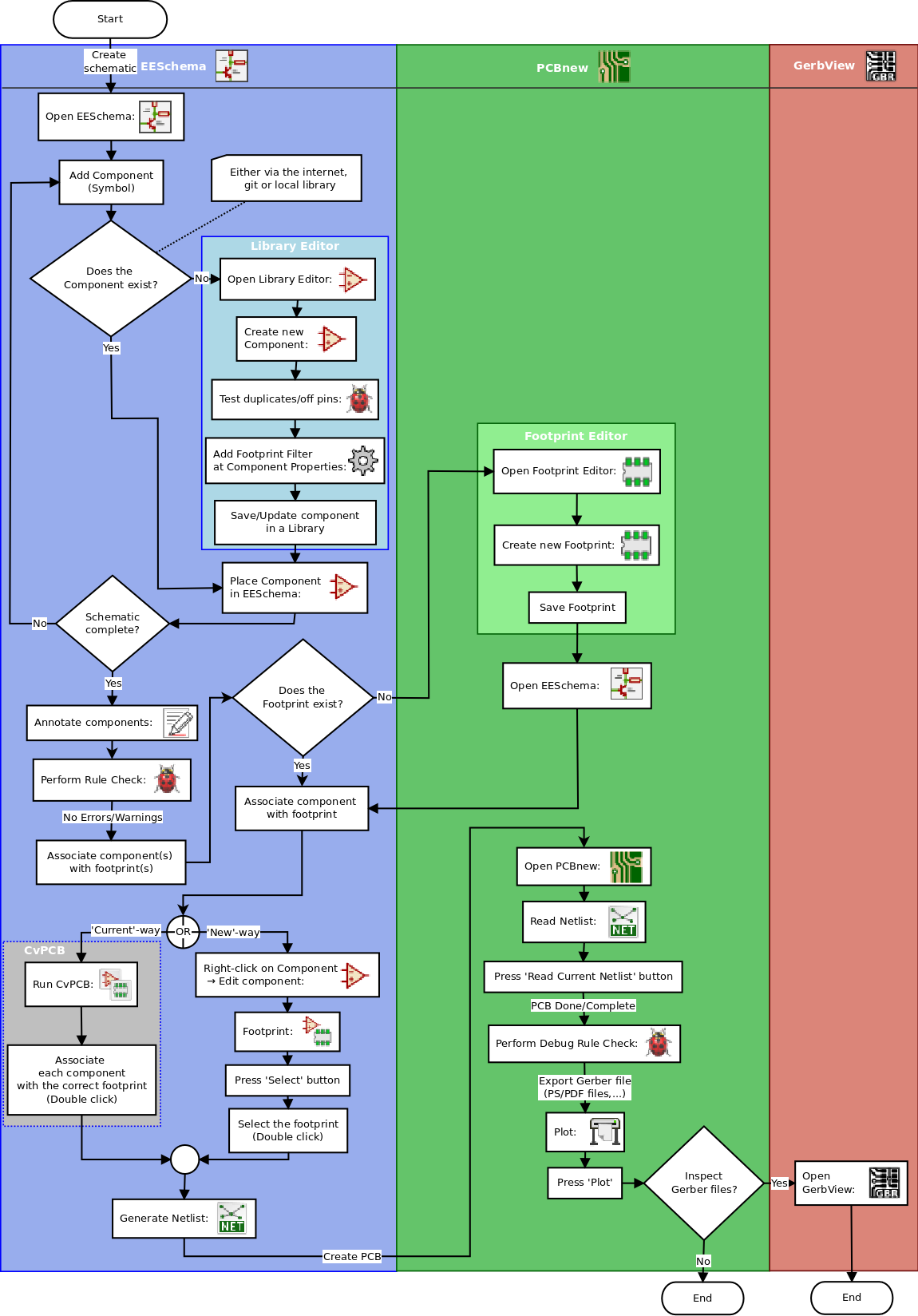
For more information about creating a component, read Making schematic symbols. And for information about how to create a new footprint, see Making component footprints.
Quicklib is a tool that allows you to quickly create KiCad library components with a web-based interface. For more information about Quicklib, refer to Making Schematic Components With Quicklib.
Forward and backward annotation
Once an electronic schematic has been fully drawn, the next step is to transfer it to a PCB. Often, additional components might need to be added, parts changed to a different size, net renamed, etc. This can be done in two ways: Forward Annotation or Backward Annotation.
Forward Annotation is the process of sending schematic information to a corresponding PCB layout. This is a fundamental feature because you must do it at least once to initially import the schematic into the PCB. Afterwards, forward annotation allows sending incremental schematic changes to the PCB. Details about Forward Annotation are discussed in the section Forward Annotation.
Backward Annotation is the process of sending a PCB layout change back to its corresponding schematic. Two common causes for Backward Annotation are gate swaps and pin swaps. In these situations, there are gates or pins which are functionally equivalent, but it may only be during layout that there is a strong case for choosing the exact gate or pin. Once the choice is made in the PCB, this change is then pushed back to the schematic.
Using KiCad
Shortcut keys
KiCad has two kinds of related but different shortcut keys: accelerator keys and hotkeys. Both are used to speed up working in KiCad by using the keyboard instead of the mouse to change commands.
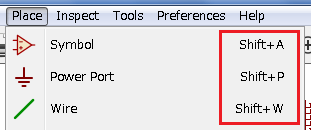
Accelerator keys
Accelerator keys have the same effect as clicking on a menu or toolbar icon: the command will be entered but nothing will happen until the left mouse button is clicked. Use an accelerator key when you want to enter a command mode but do not want any immediate action.
Accelerator keys are shown on the right side of all menu panes:
Hotkeys
A hotkey is equal to an accelerator key plus a left mouse click. Using a hotkey starts the command immediately at the current cursor location. Use a hotkey to quickly change commands without interrupting your workflow.
To view hotkeys within any KiCad tool go to Help → List Hotkeys or press Ctrl+F1:
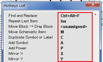
You can edit the assignment of hotkeys, and import or export them, from the Preferences → Hotkeys Options menu.
| In this document, hotkeys are expressed with brackets like this: [a]. If you see [a], just type the "a" key on the keyboard. |
Example
Consider the simple example of adding a wire in a schematic.
To use an accelerator key, press "Shift + W" to invoke the "Add wire" command (note the cursor will change). Next, left click on the desired wire start location to begin drawing the wire.
With a hotkey, simply press [w] and the wire will immediately start from the current cursor location.
Draw electronic schematics
In this section we are going to learn how to draw an electronic schematic using KiCad.
Using Eeschema
-
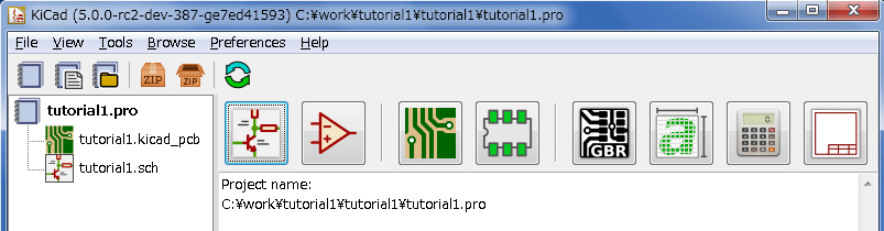
Under Windows run kicad.exe. Under Linux type 'kicad' in your Terminal. You are now in the main window of the KiCad project manager. From here you have access to eight stand-alone software tools: Eeschema, Schematic Library Editor, Pcbnew, PCB Footprint Editor, GerbView, Bitmap2Component, PCB Calculator and Pl Editor. Refer to the work-flow chart to give you an idea how the main tools are used.
-
Create a new project: File → New → Project. Name the project file 'tutorial1'. The project file will automatically take the extension ".pro". The exact appearance of the dialog depends on the used platform, but there should be a checkbox for creating a new directory. Let it stay checked unless you already have a dedicated directory. All your project files will be saved there.
-
Let’s begin by creating a schematic. Start the schematic editor Eeschema,
 . It is the first
button from the left.
. It is the first
button from the left. -
Click on the 'Page Settings' icon
 on the top
toolbar. Set the appropriate 'paper size' ('A4','8.5x11' etc.)
and enter the Title as 'Tutorial1'.
You will see that more information can be entered here if
necessary. Click OK. This information will populate the schematic
sheet at the bottom right corner. Use the mouse wheel to zoom in.
Save the whole schematic: File → Save
on the top
toolbar. Set the appropriate 'paper size' ('A4','8.5x11' etc.)
and enter the Title as 'Tutorial1'.
You will see that more information can be entered here if
necessary. Click OK. This information will populate the schematic
sheet at the bottom right corner. Use the mouse wheel to zoom in.
Save the whole schematic: File → Save -
We will now place our first component. Click on the 'Place symbol' icon
 in the right toolbar. You may also press the 'Add Symbol' hotkey [a].
 -
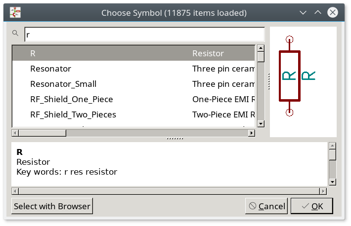
Click on the middle of your schematic sheet. A Choose Symbol window will appear on the screen. We’re going to place a resistor. Search / filter on the 'R' of Resistor. You may notice the 'Device' heading above the Resistor. This 'Device' heading is the name of the library where the component is located, which is quite a generic and useful library.
-
Double click on it. This will close the 'Choose Symbol' window. Place the component in the schematic sheet by clicking where you want it to be.
-
Click on the magnifier icon to zoom in on the component. Alternatively, use the mouse wheel to zoom in and zoom out. Press the wheel (central) mouse button to pan horizontally and vertically.
-
Try to hover the mouse over the component 'R' and press [r]. The component should rotate. You do not need to actually click on the component to rotate it.
Sometimes, if your mouse is also over something else, a menu will appear. You will see the Clarify Selection menu often in KiCad; it allows working on objects that are on top of each other. In this case, tell KiCad you want to perform the action on the 'Symbol …R…' if the menu appears. -
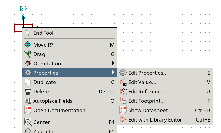
Right click in the middle of the component and select Properties → Edit Value. You can achieve the same result by hovering over the component and pressing [v]. Alternatively, [e] will take you to the more general Properties window. Notice how the right-click menu below shows the hotkeys for all available actions.
-
The Edit Value Field window will appear. Replace the current value 'R' with '1 k'. Click OK.
Do not change the Reference field (R?), this will be done automatically later on. The value above the resistor should now be '1 k'. 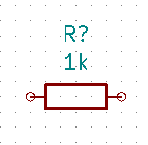
-
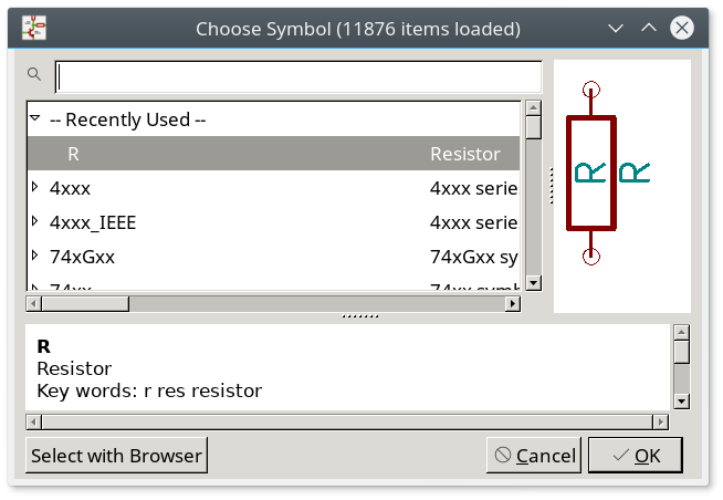
To place another resistor, simply click where you want the resistor to appear. The symbol selection window will appear again.
-
The resistor you previously chose is now in your history list, appearing as 'R'. Click OK and place the component.
-
In case you make a mistake and want to delete a component, right click on the component and click 'Delete'. This will remove the component from the schematic. Alternatively, you can hover over the component you want to delete and press [Delete].
-
You can also duplicate a component already on your schematic sheet by hovering over it and pressing [c]. Click where you want to place the new duplicated component.
-
Right click on the second resistor. Select 'Drag'. Reposition the component and left click to drop. The same functionality can be achieved by hovering over the component and by pressing [g]. [r] will rotate the component while [x] and [y] will flip it about its x- or y-axis.
Right-Click → Move or [m] is also a valuable option for moving anything around, but it is better to use this only for component labels and components yet to be connected. We will see later on why this is the case. -
Edit the second resistor by hovering over it and pressing [v]. Replace 'R' with '100'. You can undo any of your editing actions with Ctrl+Z.
-
Change the grid size. You have probably noticed that on the schematic sheet all components are snapped onto a large pitch grid. You can easily change the size of the grid by Right-Click → Grid. In general, it is recommended to use a grid of 50.0 mils for the schematic sheet.
-
We are going to add a component from a library that may not be configured in the default project. In the menu, choose Preferences → Manage Symbol Libraries. In the Symbol Libraries window you can see two tabs: Global Libraries and Project Specific Libraries. Each one has one sym-lib-table file. For a library (.lib file) to be available it must be in one of those sym-lib-table files. If you have a library file in your file system and it’s not yet available, you can add it to either one of the sym-lib-table files. For practice we will now add a library which already is available.
-
Select the Project Specific table. Click the file browser button below the table. You need to find where the official KiCad libraries are installed on your computer. Look for a
librarydirectory containing a hundred of.dcmand.libfiles. Try inC:\Program Files (x86)\KiCad\share\(Windows) and/usr/share/kicad/library/(Linux). When you have found the directory, choose and add the 'MCU_Microchip_PIC12.lib' library and close the window. It will be added to the end of of the list. Now click its nickname and change it to 'microchip_pic12mcu'. Close the Symbol Libraries window with OK. -
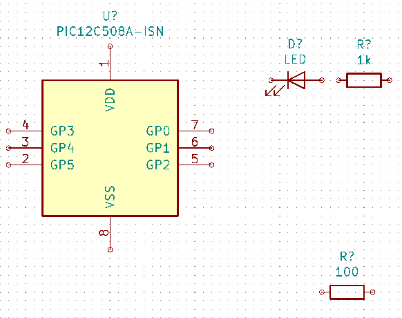
Repeat the add-component steps, however this time select the 'microchip_pic12mcu' library instead of the 'Device' library and pick the 'PIC12C508A-ISN' component.
-
Hover the mouse over the microcontroller component. Notice that [x] and [y] again flip the component. Keep the symbol mirrored around the Y axis so that the pins G0 and G1 point to right.
-
Repeat the add-component steps, this time choosing the 'Device' library and picking the 'LED' component from it.
-
Organise all components on your schematic sheet as shown below.
-
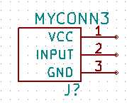
We now need to create the schematic component 'MYCONN3' for our 3-pin connector. You can jump to the section titled Make Schematic Symbols in KiCad to learn how to make this component from scratch and then return to this section to continue with the board.
-
You can now place the freshly made component. Press [a] and pick the 'MYCONN3' component in the 'myLib' library.
-
The component identifier 'J?' will appear under the 'MYCONN3' label. If you want to change its position, right click on 'J?' and click on 'Move Field' (equivalent to [m]). It might be helpful to zoom in before/while doing this. Reposition 'J?' under the component as shown below. Labels can be moved around as many times as you please.
-
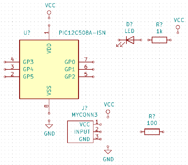
It is time to place the power and ground symbols. Click on the 'Place power port' button
 on
the right toolbar. Alternatively, press [p]. In the component
selection window, scroll down and select 'VCC' from the 'power' library.
Click OK.
on
the right toolbar. Alternatively, press [p]. In the component
selection window, scroll down and select 'VCC' from the 'power' library.
Click OK. -
Click above the pin of the 1 k resistor to place the VCC part. Click on the area above the microcontroller 'VDD'. In the 'Component Selection history' section select 'VCC' and place it next to the VDD pin. Repeat the add process again and place a VCC part above the VCC pin of 'MYCONN3'. Move references and values out of the way if needed.
-
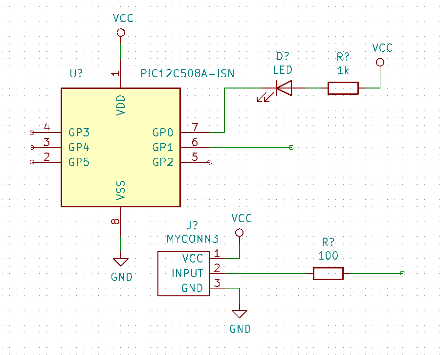
Repeat the add-pin steps but this time select the GND part. Place a GND part under the GND pin of 'MYCONN3'. Place another GND symbol on the left of the VSS pin of the microcontroller. Your schematic should now look something like this:
-
Next, we will wire all our components. Click on the 'Place wire' icon
 on the right
toolbar.
on the right
toolbar.Be careful not to pick 'Place bus', which appears directly beneath this button but has thicker lines. The section Bus Connections in KiCad will explain how to use a bus section. -
Click on the little circle at the end of pin 7 of the microcontroller and then click on the little circle on pin 1 of the LED. Click once when you are drawing the wire to create a corner. You can zoom in while you are placing the connection.
If you want to reposition wired components, it is important to use [g] (to grab) and not [m] (to move). Using grab will keep the wires connected. Review step 24 in case you have forgotten how to move a component. 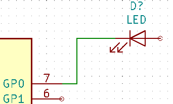
-
Repeat this process and wire up all the other components as shown below. To terminate a wire just double-click. When wiring up the VCC and GND symbols, the wire should touch the bottom of the VCC symbol and the middle top of the GND symbol. See the screenshot below.
-
We will now consider an alternative way of making a connection using labels. Pick a net labelling tool by clicking on the 'Place net label' icon
 on the right toolbar. You can also use [l].
 -
Click in the middle of the wire connected to pin 6 of the microcontroller. Name this label 'INPUT'. The label is still an independent item which you can for example move, rotate and delete. The small anchor rectangle of the label must be exactly on a wire or a pin for the label to take effect.
-
Follow the same procedure and place another label on line on the right of the 100 ohm resistor. Also name it 'INPUT'. The two labels, having the same name, create an invisible connection between pin 6 of the PIC and the 100 ohm resistor. This is a useful technique when connecting wires in a complex design where drawing the lines would make the whole schematic messier. To place a label you do not necessarily need a wire, you can simply attach the label to a pin.
-
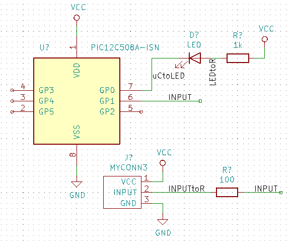
Labels can also be used to simply label wires for informative purposes. Place a label on pin 7 of the PIC. Enter the name 'uCtoLED'. Name the wire between the resistor and the LED as 'LEDtoR'. Name the wire between 'MYCONN3' and the resistor as 'INPUTtoR'.
-
You do not have to label the VCC and GND lines because the labels are implied from the power objects they are connected to.
-
Below you can see what the final result should look like.
-
Let’s now deal with unconnected wires. Any pin or wire that is not connected will generate a warning when checked by KiCad. To avoid these warnings you can either instruct the program that the unconnected wires are deliberate or manually flag each unconnected wire or pin as unconnected.
-
Click on the 'Place no connection flag' icon
 on the right toolbar. Click on
pins 2, 3, 4 and 5. An X will appear to signify that the lack of a
wire connection is intentional.
on the right toolbar. Click on
pins 2, 3, 4 and 5. An X will appear to signify that the lack of a
wire connection is intentional.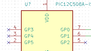
-
Some components have power pins that are invisible. You can make them visible by clicking on the 'Show hidden pins' icon
 on the left
toolbar. Hidden power pins get automatically connected if VCC and
GND naming is respected. Generally speaking, you should try not to
make hidden power pins.
on the left
toolbar. Hidden power pins get automatically connected if VCC and
GND naming is respected. Generally speaking, you should try not to
make hidden power pins. -
It is now necessary to add a 'Power Flag' to indicate to KiCad that power comes in from somewhere. Press [a] and search for 'PWR_FLAG' which is in 'power' library. Place two of them. Connect them to a GND pin and to VCC as shown below.
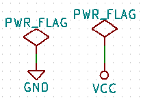
This will avoid the classic schematic checking warning: Pin connected to some other pins but no pin to drive it. -
Sometimes it is good to write comments here and there. To add comments on the schematic use the 'Place text' icon
 on the right toolbar.
 -
All components now need to have unique identifiers. In fact, many of our components are still named 'R?' or 'J?'. Identifier assignation can be done automatically by clicking on the 'Annotate schematic symbols' icon
 on the top
toolbar.
on the top
toolbar. -
In the Annotate Schematic window, select 'Use the entire schematic' and click on the 'Annotate' button. Click 'Close'. Notice how all the '?' have been replaced with numbers. Each identifier is now unique. In our example, they have been named 'R1', 'R2', 'U1', 'D1' and 'J1'.
-
We will now check our schematic for errors. Click on the 'Perform electrical rules check' icon
 on the top
toolbar. Click on the 'Run' button. A report informing you of any errors or
warnings such as disconnected wires is generated. You should have 0 Errors
and 0 Warnings. In case of errors or warnings, a small green arrow will
appear on the schematic in the position where the error or the warning is
located. Check 'Create ERC file report' and press the 'Run' button again to
receive more information about the errors.
on the top
toolbar. Click on the 'Run' button. A report informing you of any errors or
warnings such as disconnected wires is generated. You should have 0 Errors
and 0 Warnings. In case of errors or warnings, a small green arrow will
appear on the schematic in the position where the error or the warning is
located. Check 'Create ERC file report' and press the 'Run' button again to
receive more information about the errors.If you have a warning with "No default editor found, you must choose it", try setting the path to c:\windows\notepad.exe(windows) or/usr/bin/gedit(Linux). -
The schematic is now finished. We can now create a Netlist file to which we will add the footprint of each component. Click on the 'Generate netlist' icon
 on
the top toolbar. Click on the 'Generate Netlist' button and save
under the default file name.
on
the top toolbar. Click on the 'Generate Netlist' button and save
under the default file name.Netlist was necessary in previous versions of KiCad. In the recent versions you can ignore it and instead use Tools → Update PCB from Schematic. If you do that you have to assign footprints to symbols first. -
After generating the Netlist file, click on the 'Run Cvpcb' icon
 on the top
toolbar. If a missing file error window pops up, just ignore it
and click OK.
on the top
toolbar. If a missing file error window pops up, just ignore it
and click OK.There are many more ways to add footprints to symbols.
-
Right click on a symbol → Properties → Edit Footprint
-
Double click on a symbol, or right click on a symbol → Properties → Edit Properties → Footprint
-
Tools → Edit Symbol Fields
-
Check Show footprint previews in symbol chooser in Eeschema’s preferences and select the footprint when you select a new symbol to place
-
-
Cvpcb allows you to link all the components in your schematic with footprints in the KiCad library. The pane on the center shows all the components used in your schematic. Here select 'D1'. In the pane on the right you have all the available footprints, here scroll down to 'LED_THT:LED-D5.0mm' and double click on it.
-
It is possible that the pane on the right shows only a selected subgroup of available footprints. This is because KiCad is trying to suggest to you a subset of suitable footprints. Click on the icons
 ,
,
 and
and
 to
enable or disable these filters.
to
enable or disable these filters. -
For 'U1' select the 'Package_DIP:DIP-8_W7.62mm' footprint. For 'J1' select the 'Connector:Banana_Jack_3Pin' footprint. For 'R1' and 'R2' select the 'Resistor_THT:R_Axial_DIN0207_L6.3mm_D2.5mm_P2.54mm_Vertical' footprint.
-
If you are interested in knowing what the footprint you are choosing looks like, you can click on the 'View selected footprint' icon
 for a preview
of the current footprint.
for a preview
of the current footprint. -
You are done. You can save the schematic now by clicking File → Save Schematic or with the button 'Apply, Save Schematic & Continue'.
-
You can close Cvpcb and go back to the Eeschema schematic editor. If you didn’t save it in Cvpcb save it now by clicking on File → Save. Create the netlist again. Your netlist file has now been updated with all the footprints. Note that if you are missing the footprint of any device, you will need to make your own footprints. This will be explained in a later section of this document.
Now every symbol has a footprint. Instead of the net list and the next two steps you can use Tools → Update PCB from Schematic. If you do that, Pcbnew is opened with Update PCB from Schematic dialog. Click Update PCB. Then You can follow the instructions in the Pcbnew section of this tutorial. -
Switch to the KiCad project manager. You can see the net list file in the file list.
-
The netlist file describes all components and their respective pin connections. The netlist file is actually a text file that you can easily inspect, edit or script.
Library files (*.lib) are text files too and they are also easily editable or scriptable. -
To create a Bill Of Materials (BOM), go to the Eeschema schematic editor and click on the 'Generate bill of materials' icon
 on the top toolbar.
By default there is no plugin active. You add one, by clicking on
Add Plugin button. Select the *.xsl file you want to use, in
this case, we select bom2csv.xsl.
on the top toolbar.
By default there is no plugin active. You add one, by clicking on
Add Plugin button. Select the *.xsl file you want to use, in
this case, we select bom2csv.xsl.Linux:
If xsltproc is missing, you can download and install it with:
sudo apt-get install xsltproc
for a Debian derived distro like Ubuntu, or
sudo yum install xsltproc
for a RedHat derived distro. If you use neither of the two kind of distro, use your distro package manager command to install the xsltproc package.
xsl files are located at: /usr/lib/kicad/plugins/.
Apple OS X:
If xsltproc is missing, you can either install the Apple Xcode tool from the Apple site that should contain it, or download and install it with:
brew install libxslt
xsl files are located at: /Library/Application Support/kicad/plugins/.
Windows:
xsltproc.exe and the included xsl files will be located at <KiCad install directory>\bin and <KiCad install directory>\bin\scripting\plugins, respectively.
All platforms:
You can get the latest bom2csv.xsl via:
KiCad automatically generates the command, for example:xsltproc -o "%O" "/home/<user>/kicad/eeschema/plugins/bom2csv.xsl" "%I"
You may want to add the extension, so change this command line to:xsltproc -o "%O.csv" "/home/<user>/kicad/eeschema/plugins/bom2csv.xsl" "%I"
Press Help button for more info.
-
Now press 'Generate'. The file (same name as your project) is located in your project folder. Open the *.csv file with LibreOffice Calc or Excel. An import window will appear, press OK.
You are now ready to move to the PCB layout part, which is presented in the next section. However, before moving on let’s take a quick look at how to connect component pins using a bus line.
Bus connections in KiCad
Sometimes you might need to connect several sequential pins of component A with some other sequential pins of component B. In this case you have two options: the labelling method we already saw or the use of a bus connection. Let’s see how to do it.
-
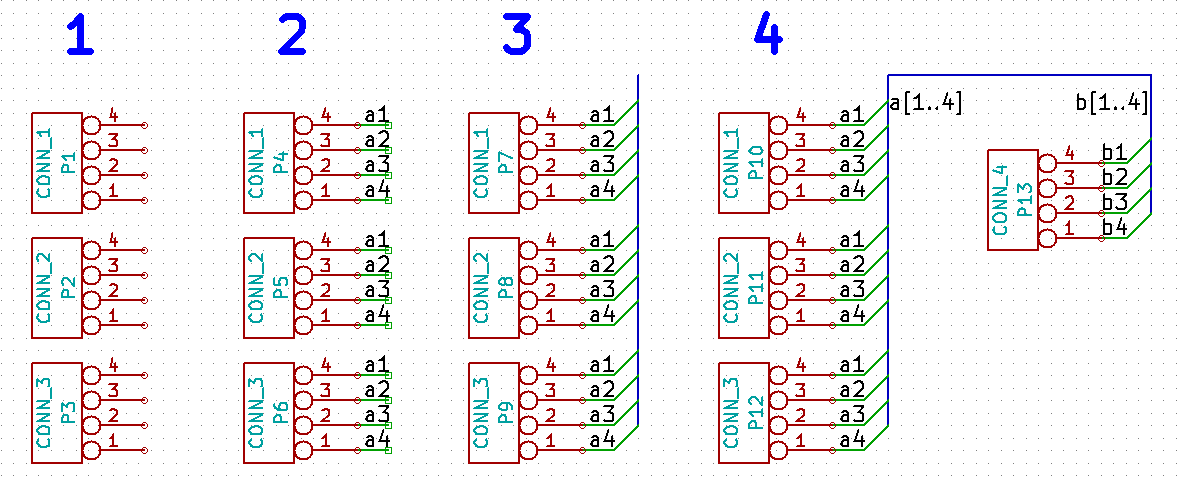
Let us suppose that you have three 4-pin connectors that you want to connect together pin to pin. Use the label option (press [l]) to label pin 4 of the P4 part. Name this label 'a1'. Now press [Insert] to have the same item automatically added on the pin below pin 4 (PIN 3). Notice how the label is automatically renamed 'a2'.
-
Press [Insert] two more times. This key corresponds to the action 'Repeat last item' and it is an infinitely useful command that can make your life a lot easier.
-
Repeat the same labelling action on the two other connectors CONN_2 and CONN_3 and you are done. If you proceed and make a PCB you will see that the three connectors are connected to each other. Figure 2 shows the result of what we described. For aesthetic purposes it is also possible to add a series of 'Place wire to bus entry' using the icon
 and bus
line using the icon
and bus
line using the icon  , as shown in Figure 3. Mind, however, that there will be no
effect on the PCB.
, as shown in Figure 3. Mind, however, that there will be no
effect on the PCB. -
It should be pointed out that the short wire attached to the pins in Figure 2 is not strictly necessary. In fact, the labels could have been applied directly to the pins.
-
Let’s take it one step further and suppose that you have a fourth connector named CONN_4 and, for whatever reason, its labelling happens to be a little different (b1, b2, b3, b4). Now we want to connect Bus a with Bus b in a pin to pin manner. We want to do that without using pin labelling (which is also possible) but by instead using labelling on the bus line, with one label per bus.
-
Connect and label CONN_4 using the labelling method explained before. Name the pins b1, b2, b3 and b4. Connect the pin to a series of 'Wire to bus entry' using the icon
and to a bus line
using the icon  . See Figure
4.
. See Figure
4. -
Put a label (press [l]) on the bus of CONN_4 and name it 'b[1..4]'.
-
Put a label (press [l]) on the previous bus and name it 'a[1..4]'.
-
What we can now do is connect bus a[1..4] with bus b[1..4] using a bus line with the button
. -
By connecting the two buses together, pin a1 will be automatically connected to pin b1, a2 will be connected to b2 and so on. Figure 4 shows what the final result looks like.
The 'Repeat last item' option accessible via [Insert] can be successfully used to repeat period item insertions. For instance, the short wires connected to all pins in Figure 2, Figure 3 and Figure 4 have been placed with this option. -
The 'Repeat last item' option accessible via [Insert] has also been extensively used to place the many series of 'Wire to bus entry' using the icon
.
Layout printed circuit boards
It is now time to use the netlist file you generated to lay out the PCB. This is done with the Pcbnew tool.
| If you used Update PCB from Schematic from Eeschema you don’t need the netlist and step 5. You can now drop the footprints into the board as in steps 6 and 7, then enter sheet information and design rules with steps 2…4. |
Using Pcbnew
-
From the KiCad project manager, click on the 'Pcb layout editor' icon
 . You can also use the
corresponding toolbar button from Eeschema.
The 'Pcbnew' window will
open. If you get a message saying that a *.kicad_pcb file
does not exist and asks if you want to create it, just click Yes.
. You can also use the
corresponding toolbar button from Eeschema.
The 'Pcbnew' window will
open. If you get a message saying that a *.kicad_pcb file
does not exist and asks if you want to create it, just click Yes. -
Begin by entering some schematic information. Click on the 'Page settings' icon
on the top
toolbar. Set the appropriate 'paper size' ('A4','8.5x11' etc.)
and 'title' as 'Tutorial1'. -
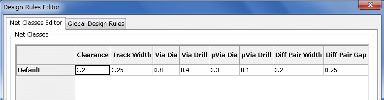
It is a good idea to start by setting the clearance and the minimum track width to those required by your PCB manufacturer. In general you can set the clearance to '0.25' and the minimum track width to '0.25'. Click on the Setup → Design Rules menu. If it does not show already, click on the 'Net Classes Editor' tab. Change the 'Clearance' field at the top of the window to '0.25' and the 'Track Width' field to '0.25' as shown below. Measurements here are in mm.
-
Click on the 'Global Design Rules' tab and set 'Minimum track width' to '0.25'. Click the OK button to commit your changes and close the Design Rules Editor window.
-
Now we will import the netlist file if you created one. Click on the 'Read netlist' icon
on the top
toolbar. The netlist file 'tutorial1.net' should be selected
in the 'Netlist file' field if it was created from Eeschema.
Click on 'Read Current Netlist'. Then click the 'Close' button. -
All components should now be visible. They are selected and follow the mouse cursor.
-
Move the components to the middle of the board. If necessary you can zoom in and out while you move the components. Click the left mouse button.
-
All components are connected via a thin group of wires called ratsnest. Make sure that the 'Show/hide board ratsnest' button
 is
pressed. In this way you can see the ratsnest linking all
components.
is
pressed. In this way you can see the ratsnest linking all
components. -
You can move each component by hovering over it and pressing [m]. Click where you want to place them. Alternatively you can select a component by clicking on it and then drag it. Press [r] to rotate a component. Move all components around until you minimise the number of wire crossovers.
-
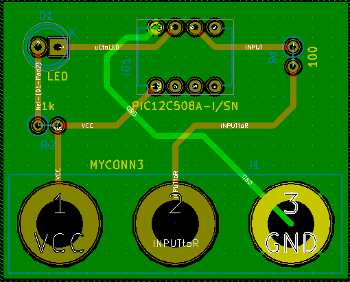
Note how one pin of the 100 ohm resistor is connected to pin 6 of the PIC component. This is the result of the labelling method used to connect pins. Labels are often preferred to actual wires because they make the schematic much less messy.
-
Now we will define the edge of the PCB. Select the 'Edge.Cuts' layer from the drop-down menu in the top toolbar. Click on the 'Add graphic lines' icon
 on the right
toolbar. Trace around the edge of the board, clicking at each
corner, and remember to leave a small gap between the edge of the
green and the edge of the PCB.
on the right
toolbar. Trace around the edge of the board, clicking at each
corner, and remember to leave a small gap between the edge of the
green and the edge of the PCB.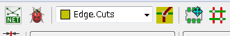
-
Next, connect up all the wires except GND. In fact, we will connect all GND connections in one go using a ground plane placed on the bottom copper (called B.Cu) of the board.
-
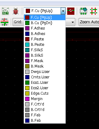
Now we must choose which copper layer we want to work on. Select 'F.Cu (PgUp)' in the drop-down menu on the top toolbar. This is the front top copper layer.
-
If you decide, for instance, to do a 4 layer PCB instead, go to Setup → Layers Setup and change 'Copper Layers' to 4. In the 'Layers' table you can name layers and decide what they can be used for. Notice that there are very useful presets that can be selected via the 'Preset Layer Groupings' menu.
-
Click on the 'Route tracks' icon
 on the right
toolbar. Click on pin 1 of 'J1' and run a track to pad
'R2'. Double-click to set the point where the track will end. The
width of this track will be the default 0.250 mm. You can change
the track width from the drop-down menu in the top toolbar. Mind
that by default you have only one track width available.
on the right
toolbar. Click on pin 1 of 'J1' and run a track to pad
'R2'. Double-click to set the point where the track will end. The
width of this track will be the default 0.250 mm. You can change
the track width from the drop-down menu in the top toolbar. Mind
that by default you have only one track width available.
-
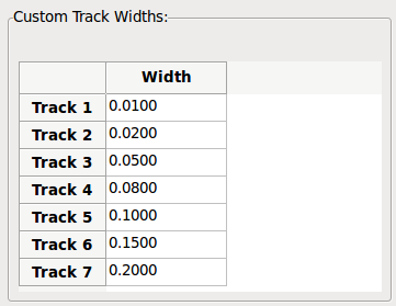
If you would like to add more track widths go to: Setup → Design Rules → Global Design Rules tab and at the bottom right of this window add any other width you would like to have available. You can then choose the widths of the track from the drop-down menu while you lay out your board. See the example below (inches).
-
Alternatively, you can add a Net Class in which you specify a set of options. Go to Setup → Design Rules → Net Classes Editor and add a new class called 'power'. Change the track width from 8 mil (indicated as 0.0080) to 24 mil (indicated as 0.0240). Next, add everything but ground to the 'power' class (select 'default' at left and 'power' at right and use the arrows).
-
If you want to change the grid size, Right click → Grid. Be sure to select the appropriate grid size before or after laying down the components and connecting them together with tracks.
-
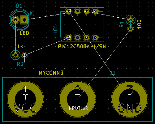
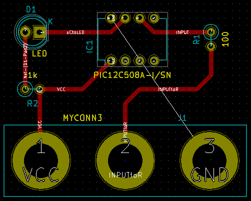
Repeat this process until all wires, except pin 3 of J1, are connected. Your board should look like the example below.
-
Let’s now run a track on the other copper side of the PCB. Select 'B.Cu' in the drop-down menu on the top toolbar. Click on the 'Route tracks' icon
. Draw a track between
pin 3 of J1 and pin 8 of U1. This is actually not necessary since
we could do this with the ground plane. Notice how the colour of
the track has changed. -
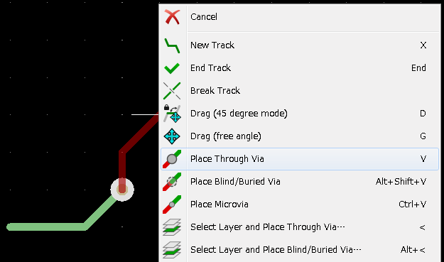
Go from pin A to pin B by changing layer. It is possible to change the copper plane while you are running a track by placing a via. While you are running a track on the upper copper plane, right click and select 'Place Via' or simply press [v]. This will take you to the bottom layer where you can complete your track.
-
When you want to inspect a particular connection you can click on the 'Highlight net' icon
 on the right
toolbar. Click on pin 3 of J1. The track itself and all pads
connected to it should become highlighted.
on the right
toolbar. Click on pin 3 of J1. The track itself and all pads
connected to it should become highlighted. -
Now we will make a ground plane that will be connected to all GND pins. Click on the 'Add filled zones' icon
 on the right toolbar. We
are going to trace a rectangle around the board, so click where
you want one of the corners to be. In the dialogue that appears,
set 'Default pad connection' to 'Thermal relief' and 'Outline slope' to
'H,V and 45 deg only' and click OK.
on the right toolbar. We
are going to trace a rectangle around the board, so click where
you want one of the corners to be. In the dialogue that appears,
set 'Default pad connection' to 'Thermal relief' and 'Outline slope' to
'H,V and 45 deg only' and click OK. -
Trace around the outline of the board by clicking each corner in rotation. Finish your rectangle by clicking the first corner second time. Right click inside the area you have just traced. Click on 'Zones'→'Fill or Refill All Zones'. The board should fill in with green and look something like this:
-
Run the design rules checker by clicking on the 'Perform design rules check' icon
 on the top
toolbar. Click on 'Start DRC'. There should be no errors. Click
on 'List Unconnected'. There should be no unconnected items. Click
OK to close the DRC Control dialogue.
on the top
toolbar. Click on 'Start DRC'. There should be no errors. Click
on 'List Unconnected'. There should be no unconnected items. Click
OK to close the DRC Control dialogue. -
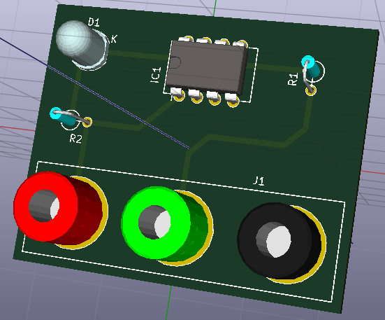
Save your file by clicking on File → Save. To admire your board in 3D, click on View → 3D Viewer.
-
You can drag your mouse around to rotate the PCB.
-
Your board is complete. To send it off to a manufacturer you will need to generate all Gerber files.
Generate Gerber files
Once your PCB is complete, you can generate Gerber files for each layer and send them to your favourite PCB manufacturer, who will make the board for you.
-
From KiCad, open the Pcbnew board editor.
-
Click on File → Plot. Select 'Gerber' as the 'Plot format' and select the folder in which to put all Gerber files. Proceed by clicking on the 'Plot' button.
-
To generate the drill file, from Pcbnew go again to the File → Plot option. Default settings should be fine.
-
These are the layers you need to select for making a typical 2-layer PCB:
| Layer | KiCad Layer Name | Default Gerber Extension | "Use Protel filename extensions" is enabled |
|---|---|---|---|
Bottom Layer |
B.Cu |
.GBR |
.GBL |
Top Layer |
F.Cu |
.GBR |
.GTL |
Top Overlay |
F.SilkS |
.GBR |
.GTO |
Bottom Solder Resist |
B.Mask |
.GBR |
.GBS |
Top Solder Resist |
F.Mask |
.GBR |
.GTS |
Edges |
Edge.Cuts |
.GBR |
.GM1 |
Using GerbView
-
To view all your Gerber files go to the KiCad project manager and click on the 'GerbView' icon. On the drop-down menu or in the Layers manager select 'Graphic layer 1'. Click on File → Open Gerber file(s) or click on the icon
 . Select and open all
generated Gerber files. Note how they all get displayed one on top
of the other.
. Select and open all
generated Gerber files. Note how they all get displayed one on top
of the other. -
Open the drill files with File → Open Excellon Drill File(s).
-
Use the Layers manager on the right to select/deselect which layer to show. Carefully inspect each layer before sending them for production.
-
The view works similarly to Pcbnew. Right click inside the view and click 'Grid' to change the grid.
Automatically route with FreeRouter
Routing a board by hand is quick and fun, however, for a board with lots of components you might want to use an autorouter. Remember that you should first route critical traces by hand and then set the autorouter to do the boring bits. Its work will only account for the unrouted traces. The autorouter we will use here is FreeRouting.
| FreeRouting is an open source java application. Currently FreeRouting exists in several more or less identical copies which you can find by doing an internet search for "freerouting". It may be found in source only form or as a precompiled java package. |
-
From Pcbnew click on File → Export → Specctra DSN and save the file locally. Launch FreeRouter and click on the 'Open Your Own Design' button, browse for the dsn file and load it.
-
FreeRouter has some features that KiCad does not currently have, both for manual routing and for automatic routing. FreeRouter operates in two main steps: first, routing the board and then optimising it. Full optimisation can take a long time, however you can stop it at any time need be.
-
You can start the automatic routing by clicking on the 'Autorouter' button on the top bar. The bottom bar gives you information about the on-going routing process. If the 'Pass' count gets above 30, your board probably can not be autorouted with this router. Spread your components out more or rotate them better and try again. The goal in rotation and position of parts is to lower the number of crossed airlines in the ratsnest.
-
Making a left-click on the mouse can stop the automatic routing and automatically start the optimisation process. Another left-click will stop the optimisation process. Unless you really need to stop, it is better to let FreeRouter finish its job.
-
Click on the File → Export Specctra Session File menu and save the board file with the .ses extension. You do not really need to save the FreeRouter rules file.
-
Back to Pcbnew. You can import your freshly routed board by clicking on File → Import → Spectra Session and selecting your .ses file.
If there is any routed trace that you do not like, you can delete it and
re-route it again, using [Delete] and the routing tool, which is the
'Route tracks' icon ![]() on the
right toolbar.
on the
right toolbar.
Forward annotation in KiCad
Once you have completed your electronic schematic, the footprint assignment, the board layout and generated the Gerber files, you are ready to send everything to a PCB manufacturer so that your board can become reality.
Often, this linear work-flow turns out to be not so uni-directional. For instance, when you have to modify/extend a board for which you or others have already completed this work-flow, it is possible that you need to move components around, replace them with others, change footprints and much more. During this modification process, what you do not want to do is to re-route the whole board again from scratch. Instead, this is how you do it:
-
Let’s suppose that you want to replace a hypothetical connector CON1 with CON2.
-
You already have a completed schematic and a fully routed PCB.
-
From KiCad, start Eeschema, make your modifications by deleting CON1 and adding CON2. Save your schematic project with the icon
 and c lick on the
'Netlist generation' icon on
the top toolbar.
and c lick on the
'Netlist generation' icon on
the top toolbar. -
Click on 'Netlist' then on 'save'. Save to the default file name. You have to rewrite the old one.
-
Now assign a footprint to CON2. Click on the 'Run Cvpcb' icon
on the top
toolbar. Assign the footprint to the new device CON2. The rest of
the components still have the previous footprints assigned to
them. Close Cvpcb. -
Back in the schematic editor, save the project by clicking on 'File' → 'Save Whole Schematic Project'. Close the schematic editor.
-
From the KiCad project manager, click on the 'Pcbnew' icon. The 'Pcbnew' window will open.
-
The old, already routed, board should automatically open. Let’s import the new netlist file. Click on the 'Read Netlist' icon
on the top toolbar. -
Click on the 'Browse Netlist Files' button, select the netlist file in the file selection dialogue, and click on 'Read Current Netlist'. Then click the 'Close' button.
-
At this point you should be able to see a layout with all previous components already routed. On the top left corner you should see all unrouted components, in our case the CON2. Select CON2 with the mouse. Move the component to the middle of the board.
-
Place CON2 and route it. Once done, save and proceed with the Gerber file generation as usual.
The process described here can easily be repeated as many times as you need. Beside the Forward Annotation method described above, there is another method known as Backward Annotation. This method allows you to make modifications to your already routed PCB from Pcbnew and updates those modifications in your schematic and netlist file. The Backward Annotation method, however, is not that useful and is therefore not described here.
Make schematic symbols in KiCad
Sometimes a symbol that you want to place on your schematic is not in a KiCad library. This is quite normal and there is no reason to worry. In this section we will see how a new schematic symbol can be quickly created with KiCad. Nevertheless, remember that you can always find KiCad components on the Internet.
In KiCad, a symbol is a piece of text that starts with 'DEF' and ends with 'ENDDEF'. One or more symbols are normally placed in a library file with the extension .lib. If you want to add symbols to a library file you can just use the cut and paste commands of a text editor.
Using Component Library Editor
-
We can use the Component Library Editor (part of Eeschema) to make new components. In our project folder 'tutorial1' let’s create a folder named 'library'. Inside we will put our new library file myLib.lib as soon as we have created our new component.
-
Now we can start creating our new component. From KiCad, start Eeschema, click on the 'Library Editor' icon
 and then click on the 'New
component' icon
and then click on the 'New
component' icon
 . The Component
Properties window will appear. Name the new component 'MYCONN3',
set the 'Default reference designator' as 'J', and the 'Number of
units per package' as '1'. Click OK. If the warning appears just
click yes.
At this point the component is only made of its labels. Let’s add
some pins. Click on the 'Add Pins' icon
. The Component
Properties window will appear. Name the new component 'MYCONN3',
set the 'Default reference designator' as 'J', and the 'Number of
units per package' as '1'. Click OK. If the warning appears just
click yes.
At this point the component is only made of its labels. Let’s add
some pins. Click on the 'Add Pins' icon
 on the right toolbar. To place the pin, left click in the centre of
the part editor sheet just below the 'MYCONN3' label.
on the right toolbar. To place the pin, left click in the centre of
the part editor sheet just below the 'MYCONN3' label. -
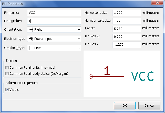
In the Pin Properties window that appears, set the pin name to 'VCC', set the pin number to '1', and the 'Electrical type' to 'Power input' then click OK.
-
Place the pin by clicking on the location you would like it to go, right below the 'MYCONN3' label.
-
Repeat the place-pin steps, this time 'Pin name' should be 'INPUT', 'Pin number' should be '2', and 'Electrical Type' should be 'Passive'.
-
Repeat the place-pin steps, this time 'Pin name' should be 'GND', 'Pin number' should be '3', and 'Electrical Type' should be 'Passive'. Arrange the pins one on top of the other. The component label 'MYCONN3' should be in the centre of the page (where the blue lines cross).
-
Next, draw the contour of the component. Click on the 'Add rectangle' icon
 . We want
to draw a rectangle next to the pins, as shown below. To do this,
click where you want the top left corner of the rectangle to be
(do not hold the mouse button down). Click again where you want
the bottom right corner of the rectangle to be.
. We want
to draw a rectangle next to the pins, as shown below. To do this,
click where you want the top left corner of the rectangle to be
(do not hold the mouse button down). Click again where you want
the bottom right corner of the rectangle to be.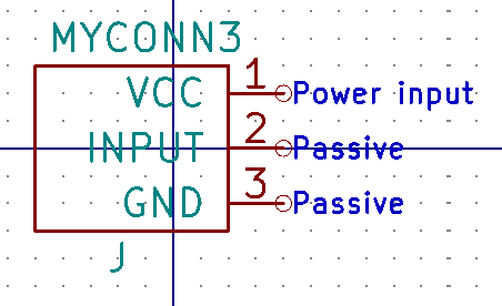
-
If you want to fill the rectangle with yellow, set the fill colour to 'yellow 4' in Preferences → Select color scheme, then select the rectangle in the editing screen with [e], selecting 'Fill background'.
-
Save the component in your library myLib.lib. Click on the 'New Library' icon
 ,
navigate into tutorial1/library/ folder and save the new library
file with the name myLib.lib.
,
navigate into tutorial1/library/ folder and save the new library
file with the name myLib.lib. -
Go to Preferences → Component Libraries and add both tutorial1/library/ in 'User defined search path' and myLib.lib in 'Component library files'.
-
Click on the 'Select working library' icon
 . In the Select Library
window click on myLib and click OK. Notice how the heading of
the window indicates the library currently in use, which now
should be myLib.
. In the Select Library
window click on myLib and click OK. Notice how the heading of
the window indicates the library currently in use, which now
should be myLib. -
Click on the 'Update current component in current library' icon
 in the top
toolbar. Save all changes by clicking on the 'Save current loaded
library on disk' icon
in the top
toolbar. Save all changes by clicking on the 'Save current loaded
library on disk' icon
 in the top
toolbar. Click 'Yes' in any confirmation messages that appear.
The new schematic component is now done and available in the
library indicated in the window title bar.
in the top
toolbar. Click 'Yes' in any confirmation messages that appear.
The new schematic component is now done and available in the
library indicated in the window title bar. -
You can now close the Component library editor window. You will return to the schematic editor window. Your new component will now be available to you from the library myLib.
-
You can make any library file.lib file available to you by adding it to the library path. From Eeschema, go to Preferences → Library and add both the path to it in 'User defined search path' and file.lib in 'Component library files'.
Export, import and modify library components
Instead of creating a library component from scratch it is sometimes easier to start from one already made and modify it. In this section we will see how to export a component from the KiCad standard library 'device' to your own library myOwnLib.lib and then modify it.
-
From KiCad, start Eeschema, click on the 'Library Editor' icon
, click on the 'Select
working library' icon and
choose the library 'device'. Click on 'Load component to edit from
the current lib' icon
 and
import the 'RELAY_2RT'.
and
import the 'RELAY_2RT'. -
Click on the 'Export component' icon
 , navigate into the library/
folder and save the new library file with the name myOwnLib.lib.
, navigate into the library/
folder and save the new library file with the name myOwnLib.lib. -
You can make this component and the whole library myOwnLib.lib available to you by adding it to the library path. From Eeschema, go to Preferences → Component Libraries and add both library/ in 'User defined search path' and myOwnLib.lib in the 'Component library files'. Close the window.
-
Click on the 'Select working library' icon
. In the Select Library
window click on myOwnLib and click OK. Notice how the heading of
the window indicates the library currently in use, it should be
myOwnLib. -
Click on the 'Load component to edit from the current lib' icon
and
import the 'RELAY_2RT'. -
You can now modify the component as you like. Hover over the label 'RELAY_2RT', press [e] and rename it 'MY_RELAY_2RT'.
-
Click on 'Update current component in current library' icon
in the top
toolbar. Save all changes by clicking on the 'Save current loaded
library on disk' icon
in the top
toolbar.
Make schematic components with quicklib
This section presents an alternative way of creating the schematic component for MYCONN3 (see MYCONN3 above) using the Internet tool quicklib.
-
Head to the quicklib web page: http://kicad.rohrbacher.net/quicklib.php
-
Fill out the page with the following information: Component name: MYCONN3 Reference Prefix: J Pin Layout Style: SIL Pin Count, N: 3
-
Click on the 'Assign Pins' icon. Fill out the page with the following information: Pin 1: VCC Pin 2: input Pin 3: GND. Type : Passive for all 3 pins.
-
Click on the icon 'Preview it' and, if you are satisfied, click on the 'Build Library Component'. Download the file and rename it tutorial1/library/myQuickLib.lib.. You are done!
-
Have a look at it using KiCad. From the KiCad project manager, start Eeschema, click on the 'Library Editor' icon
, click on the 'Import Component'
icon  , navigate to tutorial1/library/
and select myQuickLib.lib.
, navigate to tutorial1/library/
and select myQuickLib.lib.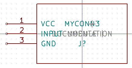
-
You can make this component and the whole library myQuickLib.lib available to you by adding it to the KiCad library path. From Eeschema, go to Preferences → Component Libraries and add library in 'User defined search path' and myQuickLib.lib in 'Component library files'.
As you might guess, this method of creating library components can be quite effective when you want to create components with a large pin count.
Make a high pin count schematic component
In the section titled Make Schematic Components in quicklib we saw how to make a schematic component using the quicklib web-based tool. However, you will occasionally find that you need to create a schematic component with a high number of pins (some hundreds of pins). In KiCad, this is not a very complicated task.
-
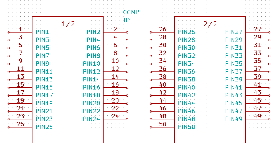
Suppose that you want to create a schematic component for a device with 50 pins. It is common practise to draw it using multiple low pin-count drawings, for example two drawings with 25 pins each. This component representation allows for easy pin connection.
-
The best way to create our component is to use quicklib to generate two 25-pin components separately, re-number their pins using a Python script and finally merge the two by using copy and paste to make them into one single DEF and ENDDEF component.
-
You will find an example of a simple Python script below that can be used in conjunction with an in.txt file and an out.txt file to re-number the line: X PIN1 1 -750 600 300 R 50 50 1 1 I into X PIN26 26 -750 600 300 R 50 50 1 1 I this is done for all lines in the file in.txt.
Simple script
#!/usr/bin/env python
''' simple script to manipulate KiCad component pins numbering'''
import sys, re
try:
    fin=open(sys.argv[1],'r')
    fout=open(sys.argv[2],'w')
except:
    print "oh, wrong use of this app, try:", sys.argv[0], "in.txt out.txt"
    sys.exit()
for ln in fin.readlines():
    obj=re.search("(X PIN)(\d*)(\s)(\d*)(\s.*)",ln)
if obj:
    num = int(obj.group(2))+25
    ln=obj.group(1) + str(num) + obj.group(3) + str(num) + obj.group(5) +'\n'
    fout.write(ln)
fin.close(); fout.close()
#
# for more info about regular expression syntax and KiCad component generation:
# http://gskinner.com/RegExr/
# http://kicad.rohrbacher.net/quicklib.php-
While merging the two components into one, it is necessary to use the Library Editor from Eeschema to move the first component so that the second does not end up on top of it. Below you will find the final .lib file and its representation in Eeschema.
Contents of a *.lib file
EESchema-LIBRARY Version 2.3
#encoding utf-8
# COMP
DEF COMP U 0 40 Y Y 1 F N
F0 "U" -1800 -100 50 H V C CNN
F1 "COMP" -1800 100 50 H V C CNN
DRAW
S -2250 -800 -1350 800 0 0 0 N
S -450 -800 450 800 0 0 0 N
X PIN1 1 -2550 600 300 R 50 50 1 1 I

...

X PIN49 49 750 -500 300 L 50 50 1 1 I
ENDDRAW
ENDDEF
#End Library
-
The Python script presented here is a very powerful tool for manipulating both pin numbers and pin labels. Mind, however, that all its power comes for the arcane and yet amazingly useful Regular Expression syntax: http://gskinner.com/RegExr/.
Make component footprints
Unlike other EDA software tools, which have one type of library that contains both the schematic symbol and the footprint variations, KiCad .lib files contain schematic symbols and .kicad_mod files contain footprints. Cvpcb is used to map footprints to symbols.
As for .lib files, .kicad_mod library files are text files that can contain anything from one to several parts.
There is an extensive footprint library with KiCad, however on occasion you might find that the footprint you need is not in the KiCad library. Here are the steps for creating a new PCB footprint in KiCad:
Using Footprint Editor
-
From the KiCad project manager start the Pcbnew tool. Click on the 'Open Footprint Editor' icon
 on the top
toolbar. This will open the 'Footprint Editor'.
on the top
toolbar. This will open the 'Footprint Editor'. -
We are going to save the new footprint 'MYCONN3' in the new footprint library 'myfootprint'. Create a new folder myfootprint.pretty in the tutorial1/ project folder. Click on the Preferences → Footprint Libraries Manager and press 'Append Library' button. In the table, enter "myfootprint" as Nickname, enter "${KIPRJMOD}/myfootprint.pretty" as Library Path and enter "KiCad" as Plugin Type. Press OK to close the PCB Library Tables window. Click on the 'Select active library' icon
 on the top toolbar.
Select the 'myfootprint' library.
on the top toolbar.
Select the 'myfootprint' library. -
Click on the 'New Footprint' icon
 on the top
toolbar. Type 'MYCONN3' as the 'footprint name'. In the middle
of the screen the 'MYCONN3' label will appear. Under the label you
can see the 'REF*' label. Right click on 'MYCONN3' and move
it above 'REF*'. Right click on 'REF__*', select 'Edit Text'
and rename it to 'SMD'. Set the 'Display' value to 'Invisible'.
on the top
toolbar. Type 'MYCONN3' as the 'footprint name'. In the middle
of the screen the 'MYCONN3' label will appear. Under the label you
can see the 'REF*' label. Right click on 'MYCONN3' and move
it above 'REF*'. Right click on 'REF__*', select 'Edit Text'
and rename it to 'SMD'. Set the 'Display' value to 'Invisible'. -
Select the 'Add Pads' icon
 on the
right toolbar. Click on the working sheet to place the pad. Right
click on the new pad and click 'Edit Pad'. You can also use [e].
on the
right toolbar. Click on the working sheet to place the pad. Right
click on the new pad and click 'Edit Pad'. You can also use [e].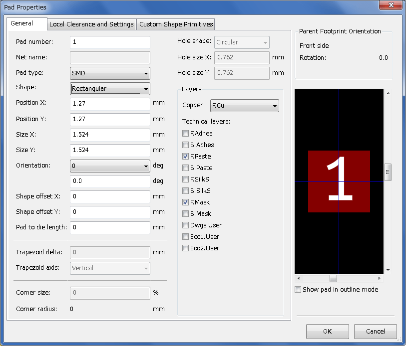
-
Set the 'Pad Num' to '1', 'Pad Shape' to 'Rect', 'Pad Type' to 'SMD', 'Shape Size X' to '0.4', and 'Shape Size Y' to '0.8'. Click OK. Click on 'Add Pads' again and place two more pads.
-
If you want to change the grid size, Right click → Grid Select. Be sure to select the appropriate grid size before laying down the components.
-
Move the 'MYCONN3' label and the 'SMD' label out of the way so that it looks like the image shown above.
-
When placing pads it is often necessary to measure relative distances. Place the cursor where you want the relative coordinate point (0,0) to be and press the space bar. While moving the cursor around, you will see a relative indication of the position of the cursor at the bottom of the page. Press the space bar at any time to set the new origin.
-
Now add a footprint contour. Click on the 'Add graphic line or polygon' button
 in
the right toolbar. Draw an outline of the connector around the
component.
in
the right toolbar. Draw an outline of the connector around the
component. -
Click on the 'Save Footprint in Active Library' icon
on the top
toolbar, using the default name MYCONN3.
Note about portability of KiCad project files
What files do you need to send to someone so that they can fully load and use your KiCad project?
When you have a KiCad project to share with somebody, it is important that the schematic file .sch, the board file .kicad_pcb, the project file .pro and the netlist file .net, are sent together with both the schematic parts file .lib and the footprints file .kicad_mod. Only this way will people have total freedom to modify the schematic and the board.
With KiCad schematics, people need the .lib files that contain the symbols. Those library files need to be loaded in the Eeschema preferences. On the other hand, with boards (.kicad_pcb files), footprints can be stored inside the .kicad_pcb file. You can send someone a .kicad_pcb file and nothing else, and they would still be able to look at and edit the board. However, when they want to load components from a netlist, the footprint libraries (.kicad_mod files) need to be present and loaded in the Pcbnew preferences just as for schematics. Also, it is necessary to load the .kicad_mod files in the preferences of Pcbnew in order for those footprints to show up in Cvpcb.
If someone sends you a .kicad_pcb file with footprints you would like to use in another board, you can open the Footprint Editor, load a footprint from the current board, and save or export it into another footprint library. You can also export all the footprints from a .kicad_pcb file at once via Pcbnew → File → Archive → Footprints → Create footprint archive, which will create a new .kicad_mod file with all the board’s footprints.
Bottom line, if the PCB is the only thing you want to distribute, then the board file .kicad_pcb is enough. However, if you want to give people the full ability to use and modify your schematic, its components and the PCB, it is highly recommended that you zip and send the following project directory:
tutorial1/
|-- tutorial1.pro
|-- tutorial1.sch
|-- tutorial1.kicad_pcb
|-- tutorial1.net
|-- library/
|   |-- myLib.lib
|   |-- myOwnLib.lib
|   \-- myQuickLib.lib
|
|-- myfootprint.pretty/
|   \-- MYCONN3.kicad_mod
|
\-- gerber/
    |-- ...
    \-- ...
More about KiCad documentation
This has been a quick guide on most of the features in KiCad. For more detailed instructions consult the help files which you can access through each KiCad module. Click on Help → Manual.
KiCad comes with a pretty good set of multi-language manuals for all its four software components.
The English version of all KiCad manuals are distributed with KiCad.
In addition to its manuals, KiCad is distributed with this tutorial, which has been translated into other languages. All the different versions of this tutorial are distributed free of charge with all recent versions of KiCad. This tutorial as well as the manuals should be packaged with your version of KiCad on your given platform.
For example, on Linux the typical locations are in the following directories, depending on your exact distribution:
/usr/share/doc/kicad/help/en/
/usr/local/share/doc/kicad/help/en
On Windows it is in:
<installation directory>/share/doc/kicad/help/en
On OS X:
/Library/Application Support/kicad/help/en
KiCad documentation on the Web
The latest version of KiCad documentation can be found in multiple languages at http://docs.kicad.org