sudo add-apt-repository ppa:js-reynaud/ppa-kicad
sudo aptitude update && sudo aptitude safe-upgrade
sudo aptitude install kicad kicad-doc-en
Guia essencial i concisa per al domini de KiCad per al desenvolupament reeixit de plaques de circuits impresos electrònics sofisticades.
Copyright
This document is Copyright © 2010-2018 by its contributors as listed below. You may distribute it and/or modify it under the terms of either the GNU General Public License (http://www.gnu.org/licenses/gpl.html), version 3 or later, or the Creative Commons Attribution License (http://creativecommons.org/licenses/by/3.0/), version 3.0 or later.
Totes les marques comercials citades en aquesta guia pertanyen als seus propietaris legítims.
Contribuïdors
David Jahshan, Phil Hutchinson, Fabrizio Tappero, Christina Jarron, Melroy van den Berg.
Traducció
Robert Antoni Buj Gelonch <[email protected]>, 2016.
Realimentació
Si us plau, adreceu aquí els vostres informes d’errors de programari, suggeriments o per a noves versions:
-
About KiCad documentation: https://gitlab.com/kicad/services/kicad-doc/issues
-
Quant al programari de KiCad: https://gitlab.com/kicad/code/kicad/issues
-
About KiCad software internationalization (i18n): https://gitlab.com/kicad/code/kicad-i18n/issues
Data de publicació
16 de maig de 2015.
Introducció a KiCad
KiCad és una eina de programari de codi obert per a la creació de diagrames d’esquemes electrònics i plaques de circuits impresos. Sota la seva aparença singular, KiCad incorpora un recull elegant de les següents eines de programari:
| Program name | Description | File extension |
|---|---|---|
KiCad |
Project manager |
*.pro |
Eeschema |
Schematic and component editor |
*.sch, *.lib, *.net |
Pcbnew |
Circuit board and footprint editor |
*.kicad_pcb, *.kicad_mod |
GerbView |
Gerber and drill file viewer |
\*.g\*, *.drl, etc. |
Bitmap2Component |
Convert bitmap images to components or footprints |
*.lib, *.kicad_mod, *.kicad_wks |
PCB Calculator |
Calculator for components, track width, electrical spacing, color codes, and more… |
None |
Pl Editor |
Page layout editor |
*.kicad_wks |
| The file extension list is not complete and only contains a subset of the files that KiCad supports. It is useful for the basic understanding of which files are used for each KiCad application. |
Es considera que KiCad està prou madur per al desenvolupament i manteniment de plaques electròniques complexes.
KiCad no presenta cap limitació quan a la mida de la placa, podeu gestionar fàcilment fins a 32 capes de coure, 14 capes tècniques i 4 capes auxiliars. KiCad pot crear tots els fitxers necessaris per a construir plaques impreses, fitxers Gerber per als foto-plòters, fitxers de perforació, fitxers d’ubicació de components i molts més.
En ser codi obert (amb llicència GPL), KiCad representa l’eina ideal per als projectes orientats a la creació de maquinari electrònic amb un gust de codi obert.
On the Internet, the homepage of KiCad is:
Downloading and installing KiCad
KiCad runs on GNU/Linux, Apple macOS and Windows. You can find the most up to date instructions and download links at:
| KiCad stable releases occur periodically per the KiCad Stable Release Policy. New features are continually being added to the development branch. If you would like to take advantage of these new features and help out by testing them, please download the latest nightly build package for your platform. Nightly builds may introduce bugs such as file corruption, generation of bad Gerbers, etc., but it is the goal of the KiCad Development Team to keep the development branch as usable as possible during new feature development. |
Sota GNU/Linux
Les versions estables de KiCad es poden trobar en la majoria dels gestors de paquets de les distribucions com a kicad i kicad-doc. Si la vostra distribució no proporciona l’última versió estable, si us plau, seguiu les instruccions de les construccions inestables i seleccioneu i instal·leu l’última versió estable.
Sota Ubuntu, la forma més senzilla per instal·lar una construcció nocturna inestable de KiCad és a través de PPA i Aptitude. Teclegeu el següent al terminal:
Under Debian, the easiest way to install backports build of KiCad is:
# Set up Debian Backports
echo -e "
# stretch-backports
deb http://ftp.us.debian.org/debian/ stretch-backports main contrib non-free
deb-src http://ftp.us.debian.org/debian/ stretch-backports main contrib non-free
" | sudo tee -a /etc/apt/sources.list > /dev/null

# Run an Update & Install KiCad
sudo apt-get update
sudo apt-get install -t stretch-backports kicad
Sota Fedora, la forma més senzilla per instal·lar una construcció nocturna inestable de KiCad és a través de copr. Per a instal·lar KiCad a través de corp teclegeu el següent:
sudo dnf copr enable @kicad/kicad
sudo dnf install kicad
També podeu baixar i instal·lar una versió precompilada de KiCad, o baixar directament el codi font, compilar i instal·lar KiCad.
Under Apple macOS
Stable builds of KiCad for macOS can be found at: https://downloads.kicad.org/kicad/macos/explore/stable
Unstable nightly development builds can be found at: https://downloads.kicad.org/kicad/macos/explore/nightlies
Sota Windows
Stable builds of KiCad for Windows can be found at: https://downloads.kicad.org/kicad/windows/explore/stable
For Windows you can find nightly development builds at: https://downloads.kicad.org/kicad/windows/explore/nightlies
Suport
Si teniu idees, comentaris o preguntes, o si simplement necessiteu ajuda:
-
Visit the Forum
-
Join users on IRC or Discord
-
Watch Tutorials
Flux de treball de KiCad
Despite its similarities with other PCB design software, KiCad is characterised by a unique workflow in which schematic components and footprints are separate. Only after creating a schematic are footprints assigned to the components.
Overview
The KiCad workflow is comprised of two main tasks: drawing the schematic and laying out the board. Both a schematic component library and a PCB footprint library are necessary for these two tasks. KiCad includes many components and footprints, and also has the tools to create new ones.
In the picture below, you see a flowchart representing the KiCad workflow. The flowchart explains which steps you need to take, and in which order. When applicable, the icon is added for convenience.
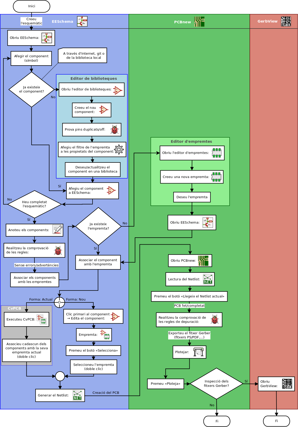
For more information about creating a component, read Making schematic symbols. And for information about how to create a new footprint, see Making component footprints.
Quicklib is a tool that allows you to quickly create KiCad library components with a web-based interface. For more information about Quicklib, refer to Making Schematic Components With Quicklib.
Anotació cap endavant i cap enrere
Once an electronic schematic has been fully drawn, the next step is to transfer it to a PCB. Often, additional components might need to be added, parts changed to a different size, net renamed, etc. This can be done in two ways: Forward Annotation or Backward Annotation.
Forward Annotation is the process of sending schematic information to a corresponding PCB layout. This is a fundamental feature because you must do it at least once to initially import the schematic into the PCB. Afterwards, forward annotation allows sending incremental schematic changes to the PCB. Details about Forward Annotation are discussed in the section Forward Annotation.
Backward Annotation is the process of sending a PCB layout change back to its corresponding schematic. Two common causes for Backward Annotation are gate swaps and pin swaps. In these situations, there are gates or pins which are functionally equivalent, but it may only be during layout that there is a strong case for choosing the exact gate or pin. Once the choice is made in the PCB, this change is then pushed back to the schematic.
Using KiCad
Shortcut keys
KiCad has two kinds of related but different shortcut keys: accelerator keys and hotkeys. Both are used to speed up working in KiCad by using the keyboard instead of the mouse to change commands.
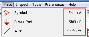
Accelerator keys
Accelerator keys have the same effect as clicking on a menu or toolbar icon: the command will be entered but nothing will happen until the left mouse button is clicked. Use an accelerator key when you want to enter a command mode but do not want any immediate action.
Accelerator keys are shown on the right side of all menu panes:
Hotkeys
A hotkey is equal to an accelerator key plus a left mouse click. Using a hotkey starts the command immediately at the current cursor location. Use a hotkey to quickly change commands without interrupting your workflow.
To view hotkeys within any KiCad tool go to Help → List Hotkeys or press Ctrl+F1:
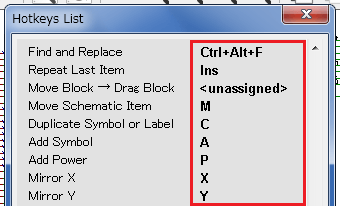
You can edit the assignment of hotkeys, and import or export them, from the Preferences → Hotkeys Options menu.
| In this document, hotkeys are expressed with brackets like this: [a]. If you see [a], just type the "a" key on the keyboard. |
Example
Consider the simple example of adding a wire in a schematic.
To use an accelerator key, press "Shift + W" to invoke the "Add wire" command (note the cursor will change). Next, left click on the desired wire start location to begin drawing the wire.
With a hotkey, simply press [w] and the wire will immediately start from the current cursor location.
Traç d’esquemes electrònics
En aquesta secció aprendrem com traçar un esquema electrònic amb KiCad.
Ús d’Eeschema
-
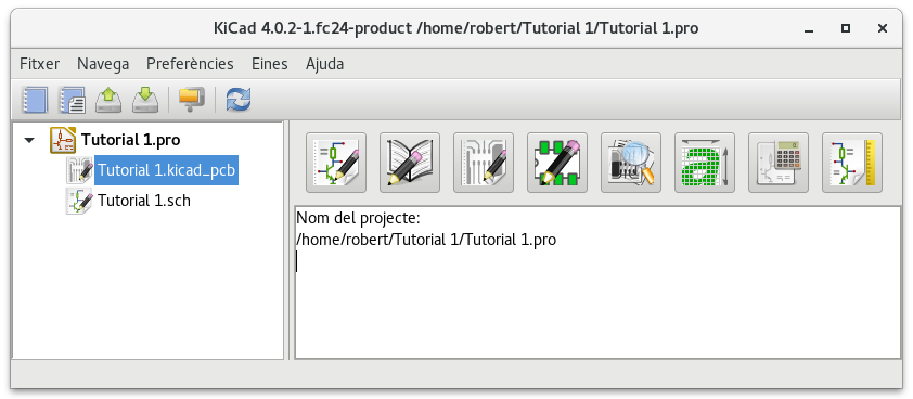
Sota Windows executeu kicad.exe. Sota Linux teclegeu 'kicad' al vostre terminal. Ara esteu davant de la finestra principal del gestor del projecte KiCad. Des d’aquí teniu accés a vuit eines de programari independents: Eeschema, Editor de biblioteques d’esquemàtics, Pcbnew, Editor d’empremtes PCB, GerbView, Bitmap2Component, Calculadora PCB i Pl Editor. Consulteu la taula del flux de treball per a tenir una idea de com s’utilitzen les eines principals.
-
Create a new project: File → New → Project. Name the project file 'tutorial1'. The project file will automatically take the extension ".pro". The exact appearance of the dialog depends on the used platform, but there should be a checkbox for creating a new directory. Let it stay checked unless you already have a dedicated directory. All your project files will be saved there.
-
Començarem amb la creació d’un esquemàtic. Inicieu l’editor d’esquemàtics Eeschema,
 . És el primer botó començant per l’esquerra.
 -
Click on the 'Page Settings' icon
 on the top toolbar. Set the appropriate 'paper size' ('A4','8.5x11' etc.) and enter the Title as 'Tutorial1'. You will see that more information can be entered here if necessary. Click OK. This information will populate the schematic sheet at the bottom right corner. Use the mouse wheel to zoom in. Save the whole schematic: File → Save
 -
We will now place our first component. Click on the 'Place symbol' icon
 in the right toolbar. You may also press the 'Add Symbol' hotkey [a].
 -
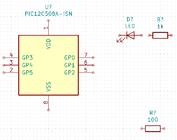
Click on the middle of your schematic sheet. A Choose Symbol window will appear on the screen. We’re going to place a resistor. Search / filter on the 'R' of Resistor. You may notice the 'Device' heading above the Resistor. This 'Device' heading is the name of the library where the component is located, which is quite a generic and useful library.
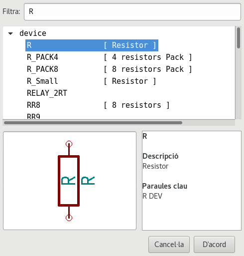
-
Double click on it. This will close the 'Choose Symbol' window. Place the component in the schematic sheet by clicking where you want it to be.
-
Feu clic a la icona de la lupa per fer zoom sobre el component. Com a alternativa, utilitzeu la roda del ratolí per apropar i allunyar la visualització. Premeu el botó de la roda (central) del ratolí per a la visió panoràmica horitzontal i vertical.
-
Try to hover the mouse over the component 'R' and press [r]. The component should rotate. You do not need to actually click on the component to rotate it.
Sometimes, if your mouse is also over something else, a menu will appear. You will see the Clarify Selection menu often in KiCad; it allows working on objects that are on top of each other. In this case, tell KiCad you want to perform the action on the 'Symbol …R…' if the menu appears. -
Right click in the middle of the component and select Properties → Edit Value. You can achieve the same result by hovering over the component and pressing [v]. Alternatively, [e] will take you to the more general Properties window. Notice how the right-click menu below shows the hotkeys for all available actions.
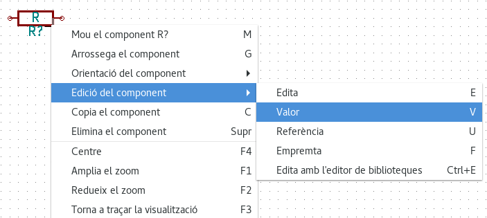
-
The Edit Value Field window will appear. Replace the current value 'R' with '1 k'. Click OK.
Do not change the Reference field (R?), this will be done automatically later on. The value above the resistor should now be '1 k'. 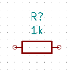
-
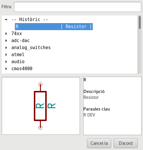
To place another resistor, simply click where you want the resistor to appear. The symbol selection window will appear again.
-
La resistència que vàreu triar prèviament ara està a la llista de l’històric, apareix com a «R». Feu clic a «D’acord» i col·loqueu el component.
-
In case you make a mistake and want to delete a component, right click on the component and click 'Delete'. This will remove the component from the schematic. Alternatively, you can hover over the component you want to delete and press [Delete].
-
You can also duplicate a component already on your schematic sheet by hovering over it and pressing [c]. Click where you want to place the new duplicated component.
-
Right click on the second resistor. Select 'Drag'. Reposition the component and left click to drop. The same functionality can be achieved by hovering over the component and by pressing [g]. [r] will rotate the component while [x] and [y] will flip it about its x- or y-axis.
Right-Click → Move or [m] is also a valuable option for moving anything around, but it is better to use this only for component labels and components yet to be connected. We will see later on why this is the case. -
Edit the second resistor by hovering over it and pressing [v]. Replace 'R' with '100'. You can undo any of your editing actions with Ctrl+Z.
-
Change the grid size. You have probably noticed that on the schematic sheet all components are snapped onto a large pitch grid. You can easily change the size of the grid by Right-Click → Grid. In general, it is recommended to use a grid of 50.0 mils for the schematic sheet.
-
We are going to add a component from a library that may not be configured in the default project. In the menu, choose Preferences → Manage Symbol Libraries. In the Symbol Libraries window you can see two tabs: Global Libraries and Project Specific Libraries. Each one has one sym-lib-table file. For a library (.lib file) to be available it must be in one of those sym-lib-table files. If you have a library file in your file system and it’s not yet available, you can add it to either one of the sym-lib-table files. For practice we will now add a library which already is available.
-
Select the Project Specific table. Click the file browser button below the table. You need to find where the official KiCad libraries are installed on your computer. Look for a
librarydirectory containing a hundred of.dcmand.libfiles. Try inC:\Program Files (x86)\KiCad\share\(Windows) and/usr/share/kicad/library/(Linux). When you have found the directory, choose and add the 'MCU_Microchip_PIC12.lib' library and close the window. It will be added to the end of of the list. Now click its nickname and change it to 'microchip_pic12mcu'. Close the Symbol Libraries window with OK. -
Repeat the add-component steps, however this time select the 'microchip_pic12mcu' library instead of the 'Device' library and pick the 'PIC12C508A-ISN' component.
-
Hover the mouse over the microcontroller component. Notice that [x] and [y] again flip the component. Keep the symbol mirrored around the Y axis so that the pins G0 and G1 point to right.
-
Repeat the add-component steps, this time choosing the 'Device' library and picking the 'LED' component from it.
-
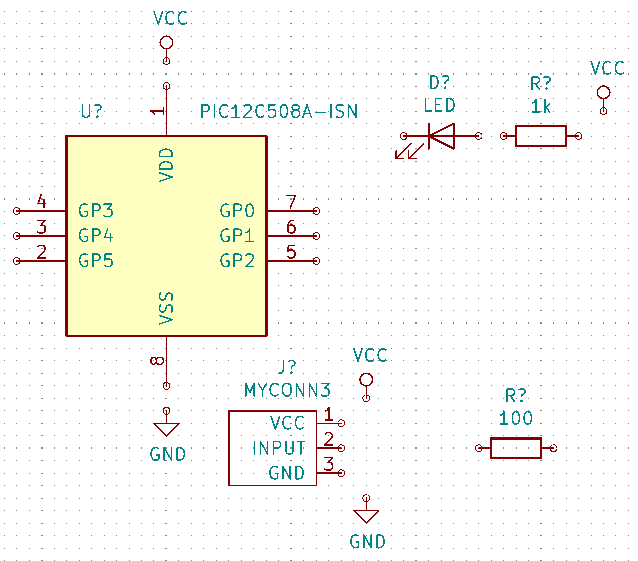
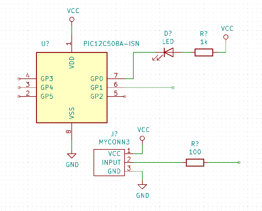
Organitzeu tots els components al vostre full de l’esquemàtic com es mostra a continuació.
-
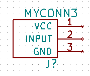
We now need to create the schematic component 'MYCONN3' for our 3-pin connector. You can jump to the section titled Make Schematic Symbols in KiCad to learn how to make this component from scratch and then return to this section to continue with the board.
-
You can now place the freshly made component. Press [a] and pick the 'MYCONN3' component in the 'myLib' library.
-
The component identifier 'J?' will appear under the 'MYCONN3' label. If you want to change its position, right click on 'J?' and click on 'Move Field' (equivalent to [m]). It might be helpful to zoom in before/while doing this. Reposition 'J?' under the component as shown below. Labels can be moved around as many times as you please.
-
It is time to place the power and ground symbols. Click on the 'Place power port' button
 on the right toolbar. Alternatively, press [p]. In the component selection window, scroll down and select 'VCC' from the 'power' library. Click OK.
 -
Click above the pin of the 1 k resistor to place the VCC part. Click on the area above the microcontroller 'VDD'. In the 'Component Selection history' section select 'VCC' and place it next to the VDD pin. Repeat the add process again and place a VCC part above the VCC pin of 'MYCONN3'. Move references and values out of the way if needed.
-
Repeat the add-pin steps but this time select the GND part. Place a GND part under the GND pin of 'MYCONN3'. Place another GND symbol on the left of the VSS pin of the microcontroller. Your schematic should now look something like this:
-
A continuació, connectarem tots els components. Feu clic a la icona «Afegeix un fil»
 de la barra d’eines de la dreta.
Be careful not to pick 'Place bus', which appears directly beneath this button but has thicker lines. The section Bus Connections in KiCad will explain how to use a bus section. -
Click on the little circle at the end of pin 7 of the microcontroller and then click on the little circle on pin 1 of the LED. Click once when you are drawing the wire to create a corner. You can zoom in while you are placing the connection.
If you want to reposition wired components, it is important to use [g] (to grab) and not [m] (to move). Using grab will keep the wires connected. Review step 24 in case you have forgotten how to move a component. 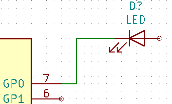
-
Repetiu aquest procés i connecteu amb fils tots els altres components, com es mostra a continuació. Per acabar un fil simplement feu doble clic. Quan afegiu el fil dels símbols VCC i GND, el fil ha de tocar el part inferior del símbol VCC i la part superior central del símbol GND. Vegeu la següent captura de pantalla.
-
We will now consider an alternative way of making a connection using labels. Pick a net labelling tool by clicking on the 'Place net label' icon
 on the right toolbar. You can also use [l].
 -
Click in the middle of the wire connected to pin 6 of the microcontroller. Name this label 'INPUT'. The label is still an independent item which you can for example move, rotate and delete. The small anchor rectangle of the label must be exactly on a wire or a pin for the label to take effect.
-
Seguiu el mateix procediment i afegiu una altra etiqueta a la línia de la dreta de la resistència de 100 ohms. Anomeneu-la també com a «INPUT». Les dues etiquetes, que tenen el mateix nom, creen una connexió invisible entre el pin 6 del PIC i la resistència de 100 ohms. Aquesta és una tècnica útil quan connecteu els fils d’un disseny complex i el traç de les línies provocaria que tot l’esquema estigués embolicat. Per a posar una etiqueta, no es necessita necessàriament un fil, només heu de posar l’etiqueta a un pin.
-
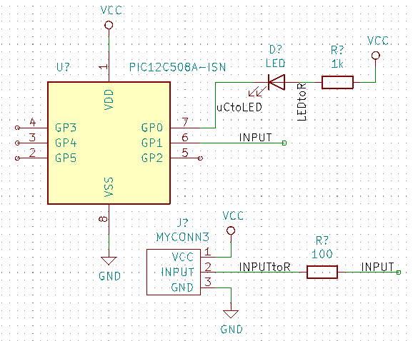
Les etiquetes també es poden utilitzar simplement per a etiquetar els fils per a fins informatius. Afegiu una etiqueta al pin 7 del PIC. Introduïu el nom «uCtoLED». Anomeneu el fil entre la resistència i el LCD com a «LEDtoR». Anomeneu el fil entre «MYCONN3» i la resistència com a «INPUTtoR».
-
No cal que etiqueteu les línies VCC i GND perquè les etiquetes s’infereixen dels objectes d’alimentació als que estan connectats.
-
A continuació es pot veure el que hauria de ser semblant al resultat final.
-
Ara ens preocuparem dels fils no connectats. Qualsevol pin o fil que no estigui connectat generarà una advertència quan KiCad realitzi una comprovació. Per a evitar aquestes advertències podeu ordenar al programa que els fils sense connectar indiquen deliberadament o manualment un fil o un pin sense connectar.
-
Click on the 'Place no connection flag' icon
 on the right toolbar. Click on pins 2, 3, 4 and 5. An X will appear to signify that the lack of a wire connection is intentional.
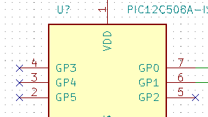
-
Alguns components tenen pins d’alimentació que són invisibles. Podeu fer-los visibles en fer clic a la icona «Mostra els pins ocults»
 de la barra d’eines de l’esquerra. Els pins d’alimentació ocults es connecten de forma automàtica si es respecta la nomenclatura VCC i GND. De forma genèrica, heu d’intentar de no crear pins d’alimentació ocults.
 -
It is now necessary to add a 'Power Flag' to indicate to KiCad that power comes in from somewhere. Press [a] and search for 'PWR_FLAG' which is in 'power' library. Place two of them. Connect them to a GND pin and to VCC as shown below.
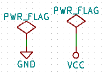
This will avoid the classic schematic checking warning: Pin connected to some other pins but no pin to drive it. -
Sometimes it is good to write comments here and there. To add comments on the schematic use the 'Place text' icon
 on the right toolbar.
 -
All components now need to have unique identifiers. In fact, many of our components are still named 'R?' or 'J?'. Identifier assignation can be done automatically by clicking on the 'Annotate schematic symbols' icon
 on the top toolbar.
 -
In the Annotate Schematic window, select 'Use the entire schematic' and click on the 'Annotate' button. Click 'Close'. Notice how all the '?' have been replaced with numbers. Each identifier is now unique. In our example, they have been named 'R1', 'R2', 'U1', 'D1' and 'J1'.
-
Ara anirem a comprovar que el nostre esquemàtic estigui lliure d’errors. Feu clic a la icona «Realitza la comprovació de les regles elèctriques»
 de la barra d’eines superior. Feu clic al botó «Executa». Es genera un informe que us informa dels errors o de les advertències, com ara fils desconnectats. Hauríeu de tenir 0 errors i 0 advertències. En cas d’errors o d’advertències, apareixerà una petita fletxa verda a l’esquemàtic en la posició on es troba l’error o l’advertència. Feu clic a «Crea el fitxer de l’informe ERC» i premeu el botó «Executa» un altre cop per a rebre més informació sobre els errors.
If you have a warning with "No default editor found, you must choose it", try setting the path to c:\windows\notepad.exe(windows) or/usr/bin/gedit(Linux). -
The schematic is now finished. We can now create a Netlist file to which we will add the footprint of each component. Click on the 'Generate netlist' icon
 on the top toolbar. Click on the 'Generate Netlist' button and save under the default file name.
Netlist was necessary in previous versions of KiCad. In the recent versions you can ignore it and instead use Tools → Update PCB from Schematic. If you do that you have to assign footprints to symbols first. -
Després de generar el fitxer Netlist, feu clic a la icona «Executa Cvpcb»
 de la barra d’eines superior. Si apareix una finestra d’error que falta un fitxer, simplement ho ignoreu i feu clic a «D’acord».
There are many more ways to add footprints to symbols.
-
Right click on a symbol → Properties → Edit Footprint Double click on a symbol, or right click on a symbol → Properties → Edit Properties → Footprint
-
Tools → Edit Symbol Fields Check Show footprint previews in symbol chooser in Eeschema’s preferences and select the footprint when you select a new symbol to place
-
-
Cvpcb allows you to link all the components in your schematic with footprints in the KiCad library. The pane on the center shows all the components used in your schematic. Here select 'D1'. In the pane on the right you have all the available footprints, here scroll down to 'LED_THT:LED-D5.0mm' and double click on it.
-
És possible que el panell de la dreta mostri només la selecció d’un subgrup d’empremtes disponibles. Això és perquè KiCad està intentant suggerir-vos un subconjunt d’empremtes adequat. Feu clic a les icones
 ,
,  and
and  per a habilitar o inhabilitar aquests filtres.
 -
For 'U1' select the 'Package_DIP:DIP-8_W7.62mm' footprint. For 'J1' select the 'Connector:Banana_Jack_3Pin' footprint. For 'R1' and 'R2' select the 'Resistor_THT:R_Axial_DIN0207_L6.3mm_D2.5mm_P2.54mm_Vertical' footprint.
-
If you are interested in knowing what the footprint you are choosing looks like, you can click on the 'View selected footprint' icon
 for a preview of the current footprint.
 -
You are done. You can save the schematic now by clicking File → Save Schematic or with the button 'Apply, Save Schematic & Continue'.
-
You can close Cvpcb and go back to the Eeschema schematic editor. If you didn’t save it in Cvpcb save it now by clicking on File → Save. Create the netlist again. Your netlist file has now been updated with all the footprints. Note that if you are missing the footprint of any device, you will need to make your own footprints. This will be explained in a later section of this document.
Now every symbol has a footprint. Instead of the net list and the next two steps you can use Tools → Update PCB from Schematic. If you do that, Pcbnew is opened with Update PCB from Schematic dialog. Click Update PCB. Then You can follow the instructions in the Pcbnew section of this tutorial. -
Switch to the KiCad project manager. You can see the net list file in the file list.
-
El fitxer netlist descriu tots els components i les seves respectives connexions dels pins. El fitxer netlist en realitat és un fitxer de text que fàcilment es pot inspeccionar, editar o crear scripts.
Els fitxers de les biblioteques (*.lib) també són fitxers de text i són fàcils d’editar i de generar scripts. -
To create a Bill Of Materials (BOM), go to the Eeschema schematic editor and click on the 'Generate bill of materials' icon
 on the top toolbar. By default there is no plugin active. You add one, by clicking on Add Plugin button. Select the *.xsl file you want to use, in this case, we select bom2csv.xsl.
Linux:
If xsltproc is missing, you can download and install it with:
sudo apt-get install xsltproc
for a Debian derived distro like Ubuntu, or
sudo yum install xsltproc
for a RedHat derived distro. If you use neither of the two kind of distro, use your distro package manager command to install the xsltproc package.
xsl files are located at: /usr/lib/kicad/plugins/.
Apple OS X:
If xsltproc is missing, you can either install the Apple Xcode tool from the Apple site that should contain it, or download and install it with:
brew install libxslt
xsl files are located at: /Library/Application Support/kicad/plugins/.
Windows:
xsltproc.exe and the included xsl files will be located at <KiCad install directory>\bin and <KiCad install directory>\bin\scripting\plugins, respectively.
All platforms:
You can get the latest bom2csv.xsl via:
KiCad genera automàticament l’ordre, per exemple:xsltproc -o "%O" "/home/<user>/kicad/eeschema/plugins/bom2csv.xsl" "%I"
És possible que vulgueu afegir-hi l’extensió, canvieu aquesta línia d’ordres a:xsltproc -o "%O.csv" "/home/<user>/kicad/eeschema/plugins/bom2csv.xsl" "%I"
Premeu el botó Ajuda per a més informació.
-
Ara premeu «Genera». El fitxer (amb el mateix nom que el vostre projecte) està ubicat a la carpeta del vostre projecte. Obriu el fitxer *.csv amb LibreOffice Calc o Excel. Apareixerà una finestra d’importació, premeu «D’acord».
Ara esteu llest per a passar a la part de la disposició del PCB, que es presenta en la següent secció. No obstant això, abans de seguir endavant anem a donar una ullada ràpida a la manera de connectar els pins dels components utilitzant una línia de bus.
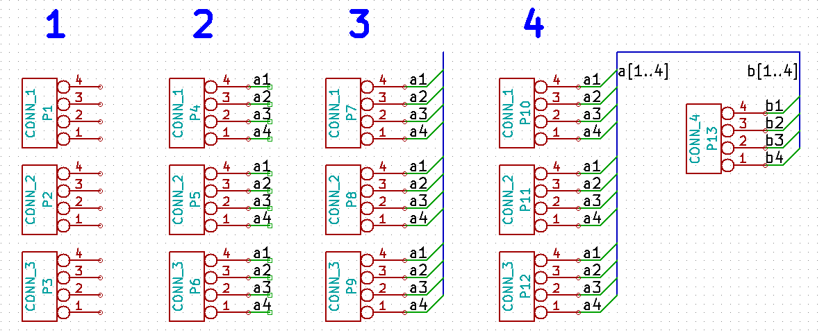
Connexions de bus en KiCad
De vegades pot ser que hàgiu de connectar diversos pins seqüencials del component A amb alguns altres pins seqüencials del component B. En aquest cas, teniu dues opcions: el mètode d’etiquetatge que ja vam veure o l’ús d’una connexió de bus. Vegem com fer-ho.
-
Let us suppose that you have three 4-pin connectors that you want to connect together pin to pin. Use the label option (press [l]) to label pin 4 of the P4 part. Name this label 'a1'. Now press [Insert] to have the same item automatically added on the pin below pin 4 (PIN 3). Notice how the label is automatically renamed 'a2'.
-
Press [Insert] two more times. This key corresponds to the action 'Repeat last item' and it is an infinitely useful command that can make your life a lot easier.
-
Repetiu la mateixa acció d’etiquetatge en els altres dos connectors, CONN_2 i CONN_3, i ja està fet. Si continueu i feu un PCB veureu que els tres connectors estan connectats entre si. La Figura 2 mostra el resultat del que estem descrivint. Per raons estètiques també és possible afegir una sèrie d'«Afegeix un fil a l’entrada del bus» amb la icona
 i la línia de bús amb la icona
  , com es mostra a la Figura 3. Tingueu present que no hi haurà cap efecte sobre el PCB.
 -
Cal assenyalar que els fils curts connectats als pins de la Figura 2 no són estrictament necessaris. De fet, les etiquetes es podrien haver aplicat directament als pins.
-
Fem un pas més enllà i suposem que teniu un quart connector anomenat CONN_4 i per qualsevol motiu el seu etiquetatge passa a ser una mica diferent (b1, b2, b3 i b4). Ara volem connectar el Bus a amb el Bus b de la manera pin a pin. Volem fer-ho sense la necessitat d’utilitzar l’etiquetatge dels pins (que també és possible), en lloc seu volem utilitzar l’etiquetatge de la línia de bus, amb una etiqueta per bus.
-
Connecteu i etiqueteu CONN_4 amb el mètode d’etiquetatge que s’ha explicat abans. Anomeneu els pins b1, b2, b3 i b4. Connecteu el pin cap a una de les sèries de «Fil a entrada del bus» mitjançant la icona
i cap a una línia de bus mitjançant la icona  . Vegeu la Figura 4.
 -
Put a label (press [l]) on the bus of CONN_4 and name it 'b[1..4]'.
-
Put a label (press [l]) on the previous bus and name it 'a[1..4]'.
-
Ara el que podem fer és connectar el bus a[1..4] amb el bus b[1..4] mitjançant una línia de bus amb el botó
. -
En connectar amb la unió els dos busos, el pin a1 es connectarà automàticament al pin b1, l’a2 es connectarà al b2 i així successivament. La figura 4 mostra el resultat final.
The 'Repeat last item' option accessible via [Insert] can be successfully used to repeat period item insertions. For instance, the short wires connected to all pins in Figure 2, Figure 3 and Figure 4 have been placed with this option. -
The 'Repeat last item' option accessible via [Insert] has also been extensively used to place the many series of 'Wire to bus entry' using the icon
.
Disposició de les plaques de circuits impresos
Ara és el moment d’utilitzar el fitxer netlist que heu generat per a disposar el PCB. Això es fa amb l’eina Pcbnew.
| If you used Update PCB from Schematic from Eeschema you don’t need the netlist and step 5. You can now drop the footprints into the board as in steps 6 and 7, then enter sheet information and design rules with steps 2…4. |
Ús de Pcbnew
-
From the KiCad project manager, click on the 'Pcb layout editor' icon
 . You can also use the corresponding toolbar button from Eeschema. The 'Pcbnew' window will open. If you get a message saying that a *.kicad_pcb file does not exist and asks if you want to create it, just click Yes.
 -
Begin by entering some schematic information. Click on the 'Page settings' icon
on the top toolbar. Set the appropriate 'paper size' ('A4','8.5x11' etc.) and 'title' as 'Tutorial1'. -
It is a good idea to start by setting the clearance and the minimum track width to those required by your PCB manufacturer. In general you can set the clearance to '0.25' and the minimum track width to '0.25'. Click on the Setup → Design Rules menu. If it does not show already, click on the 'Net Classes Editor' tab. Change the 'Clearance' field at the top of the window to '0.25' and the 'Track Width' field to '0.25' as shown below. Measurements here are in mm.
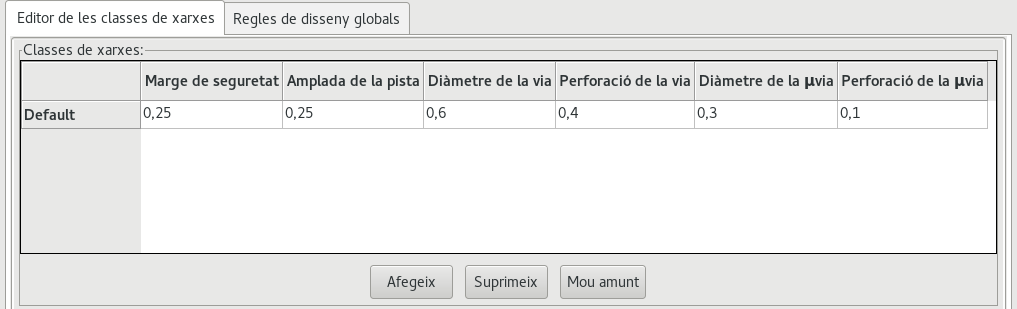
-
Click on the 'Global Design Rules' tab and set 'Minimum track width' to '0.25'. Click the OK button to commit your changes and close the Design Rules Editor window.
-
Now we will import the netlist file if you created one. Click on the 'Read netlist' icon
on the top toolbar. The netlist file 'tutorial1.net' should be selected in the 'Netlist file' field if it was created from Eeschema. Click on 'Read Current Netlist'. Then click the 'Close' button. -
All components should now be visible. They are selected and follow the mouse cursor.
-
Move the components to the middle of the board. If necessary you can zoom in and out while you move the components. Click the left mouse button.
-
All components are connected via a thin group of wires called ratsnest. Make sure that the 'Show/hide board ratsnest' button
 is pressed. In this way you can see the ratsnest linking all components.
 -
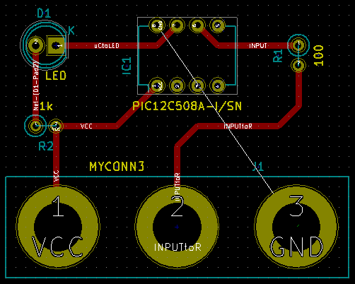
You can move each component by hovering over it and pressing [m]. Click where you want to place them. Alternatively you can select a component by clicking on it and then drag it. Press [r] to rotate a component. Move all components around until you minimise the number of wire crossovers.
-
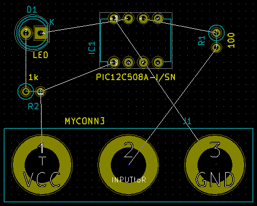
Note how one pin of the 100 ohm resistor is connected to pin 6 of the PIC component. This is the result of the labelling method used to connect pins. Labels are often preferred to actual wires because they make the schematic much less messy.
-
Now we will define the edge of the PCB. Select the 'Edge.Cuts' layer from the drop-down menu in the top toolbar. Click on the 'Add graphic lines' icon
 on the right toolbar. Trace around the edge of the board, clicking at each corner, and remember to leave a small gap between the edge of the green and the edge of the PCB.
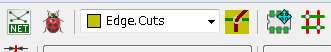
-
A continuació, connecteu tots els fils excepte GND. De fet, connectarem totes les connexions a GND d’un sol cop utilitzant un plànol de terra situat a la part inferior de coure (que s’anomena B.Cu) de la placa.
-
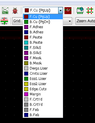
Ara hem de triar en quina capa de coure volem treballar. Seleccioneu «F.Cu (PgUp)» al menú desplegable de la barra d’eines superior. Aquesta és la capa de coure superior de la part frontal.
-
If you decide, for instance, to do a 4 layer PCB instead, go to Setup → Layers Setup and change 'Copper Layers' to 4. In the 'Layers' table you can name layers and decide what they can be used for. Notice that there are very useful presets that can be selected via the 'Preset Layer Groupings' menu.
-
Click on the 'Route tracks' icon
 on the right toolbar. Click on pin 1 of 'J1' and run a track to pad 'R2'. Double-click to set the point where the track will end. The width of this track will be the default 0.250 mm. You can change the track width from the drop-down menu in the top toolbar. Mind that by default you have only one track width available.
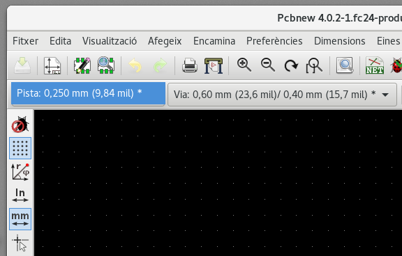
-
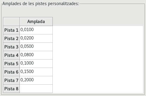
If you would like to add more track widths go to: Setup → Design Rules → Global Design Rules tab and at the bottom right of this window add any other width you would like to have available. You can then choose the widths of the track from the drop-down menu while you lay out your board. See the example below (inches).
-
Alternatively, you can add a Net Class in which you specify a set of options. Go to Setup → Design Rules → Net Classes Editor and add a new class called 'power'. Change the track width from 8 mil (indicated as 0.0080) to 24 mil (indicated as 0.0240). Next, add everything but ground to the 'power' class (select 'default' at left and 'power' at right and use the arrows).
-
If you want to change the grid size, Right click → Grid. Be sure to select the appropriate grid size before or after laying down the components and connecting them together with tracks.
-
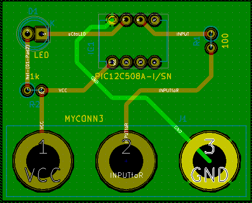
Repetiu aquest procés fins que tots els cables estiguin connectats, excepte el pin 3 de J1. La placa hauria de ser quelcom similar al següent exemple.
-
Let’s now run a track on the other copper side of the PCB. Select 'B.Cu' in the drop-down menu on the top toolbar. Click on the 'Route tracks' icon
. Draw a track between pin 3 of J1 and pin 8 of U1. This is actually not necessary since we could do this with the ground plane. Notice how the colour of the track has changed. -
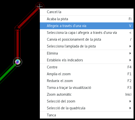
Go from pin A to pin B by changing layer. It is possible to change the copper plane while you are running a track by placing a via. While you are running a track on the upper copper plane, right click and select 'Place Via' or simply press [v]. This will take you to the bottom layer where you can complete your track.
-
When you want to inspect a particular connection you can click on the 'Highlight net' icon
 on the right toolbar. Click on pin 3 of J1. The track itself and all pads connected to it should become highlighted.
 -
Now we will make a ground plane that will be connected to all GND pins. Click on the 'Add filled zones' icon
 on the right toolbar. We are going to trace a rectangle around the board, so click where you want one of the corners to be. In the dialogue that appears, set 'Default pad connection' to 'Thermal relief' and 'Outline slope' to 'H,V and 45 deg only' and click OK.
 -
Trace around the outline of the board by clicking each corner in rotation. Finish your rectangle by clicking the first corner second time. Right click inside the area you have just traced. Click on 'Zones'→'Fill or Refill All Zones'. The board should fill in with green and look something like this:
-
Run the design rules checker by clicking on the 'Perform design rules check' icon
 on the top toolbar. Click on 'Start DRC'. There should be no errors. Click on 'List Unconnected'. There should be no unconnected items. Click OK to close the DRC Control dialogue.
 -
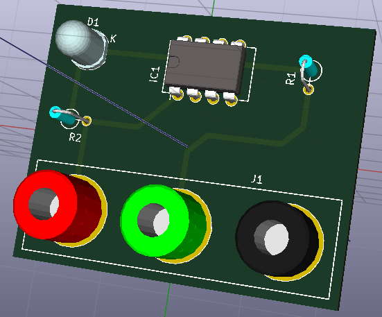
Deseu el vostre fitxer en fer clic a Fitxer → Desa. Per admirar la vostra placa en 3D, feu clic a Visualització → Visualitzador 3D.
-
Podeu arrossegar el vostre ratolí per tot arreu per a girar el PCB.
-
La placa ja està completada. Per a enviar-ho a un fabricant haureu de generar tots els fitxers Gerber.
Generació dels fitxers Gerber
Una vegada que hàgiu completat el vostre PCB, podeu generar els fitxers Gerber per a cadascuna de les capes i enviar-ho al vostre fabricant favorit de plaques de circuits impresos, qui us farà la placa.
-
From KiCad, open the Pcbnew board editor.
-
Click on File → Plot. Select 'Gerber' as the 'Plot format' and select the folder in which to put all Gerber files. Proceed by clicking on the 'Plot' button.
-
Per a generar el fitxer de perforació, des de Pcbnew torneu a anar a Fitxer → Ploteja. Els ajusts predeterminats estan prou bé.
-
Aquestes són les capes que heu de seleccionar per a la fabricació d’un PCB típic de 2 capes:
| Layer | KiCad Layer Name | Default Gerber Extension | "Use Protel filename extensions" is enabled |
|---|---|---|---|
Bottom Layer |
B.Cu |
.GBR |
.GBL |
Top Layer |
F.Cu |
.GBR |
.GTL |
Top Overlay |
F.SilkS |
.GBR |
.GTO |
Bottom Solder Resist |
B.Mask |
.GBR |
.GBS |
Top Solder Resist |
F.Mask |
.GBR |
.GTS |
Edges |
Edge.Cuts |
.GBR |
.GM1 |
Ús de GerbView
-
To view all your Gerber files go to the KiCad project manager and click on the 'GerbView' icon. On the drop-down menu or in the Layers manager select 'Graphic layer 1'. Click on File → Open Gerber file(s) or click on the icon
 . Select and open all generated Gerber files. Note how they all get displayed one on top of the other.
 -
Open the drill files with File → Open Excellon Drill File(s).
-
Use the Layers manager on the right to select/deselect which layer to show. Carefully inspect each layer before sending them for production.
-
The view works similarly to Pcbnew. Right click inside the view and click 'Grid' to change the grid.
Encaminament automàtic amb FreeRouter
Routing a board by hand is quick and fun, however, for a board with lots of components you might want to use an autorouter. Remember that you should first route critical traces by hand and then set the autorouter to do the boring bits. Its work will only account for the unrouted traces. The autorouter we will use here is FreeRouting.
| FreeRouting is an open source java application. Currently FreeRouting exists in several more or less identical copies which you can find by doing an internet search for "freerouting". It may be found in source only form or as a precompiled java package. |
-
From Pcbnew click on File → Export → Specctra DSN and save the file locally. Launch FreeRouter and click on the 'Open Your Own Design' button, browse for the dsn file and load it.
-
FreeRouter té algunes característiques que KiCad no té actualment, tant l’encaminament manual com l’encaminament automàtic. FreeRouter funciona en dos passos principals: en primer lloc, realitza l’encaminament de la placa i després realitza l’optimització. L’optimització completa pot trigar molt de temps, però es pot aturar en qualsevol moment quan calgui.
-
Podeu iniciar l’encaminament automàtic en fer clic el botó «Autorouter» de la barra d’eines superior. La barra inferior proporciona informació sobre el procés en marxa d’encaminament. Si el comptador «Pass» arriba a les 30 passades, probablement la vostra placa no es pot encaminar amb aquest encaminador. Separeu una mica més els vostres components o gireu-los millor, després torneu a intentar-ho. L’objectiu de girar i posicionar les peces és reduir el nombre de línies de les línies aèries creuades a l’embolic.
-
Si feu un clic amb el botó secundari del ratolí podeu aturar l’encaminament automàtic i iniciar automàticament el procés d’optimització. Un altre clic amb el botó secundar aturarà el procés d’optimització. Llevat que realment necessiteu parar-ho, és millor deixar que FreeRouter acabi la feina.
-
Feu clic al menú Fitxer → Exporta el fitxer de Specctra Session i deseu el fitxer de la placa amb l’extensió .ses. En realitat, no cal que deseu el fitxer de les regles de FreeRouter.
-
Back to Pcbnew. You can import your freshly routed board by clicking on File → Import → Spectra Session and selecting your .ses file.
If there is any routed trace that you do not like, you can delete it and re-route it again, using [Delete] and the routing tool, which is the 'Route tracks' icon ![]() on the right toolbar.
on the right toolbar.
Anotació cap endavant en KiCad
Un cop hàgiu completat el vostre esquema electrònic, l’assignació de les empremtes, la disposició de la placa i la generació dels fitxers Gerber, ja esteu preparat per a enviar-ho tot a un fabricant de PCB de manera que la placa ja pot esdevenir real.
Sovint, aquest flux de treball lineal resulta que no és no tan unidireccional. Per exemple, quan heu de modificar o ampliar una placa per a la qual tu mateix o altres persones ja hagin completat aquest flux de treball, és possible que necessiteu moure els components, substituir-los per altres, canviar les empremtes, entre altres. En el transcurs d’aquest procés de modificació, el que segurament no voleu tornar a fer és modificar de nou l’encaminament de tota la placa des de zero. En el seu lloc, ho podeu fer així:
-
Suposem que voleu canviar un connector hipotètic CON1 amb CON2.
-
Ja teniu un esquema complet i un PCB amb tot l’encaminament.
-
Des de KiCad, inicieu Eeschema, feu les vostres modificacions amb l’eliminació de CON1 i amb l’addició de CON2. Deseu el vostre projecte d’esquemàtic
 i feu clic a la icona «Generació del netlist» de la barra d’eines superior.
 -
Feu clic a «Netlist» i després a «Desa». Deseu-ho amb el nom de fitxer predeterminat. Heu de tornar a escriure l’antic.
-
Ara assigneu l’empremta a CON2. Feu clic a la icona «Executa Cvpcb»
de la barra d’eines superior. Assigneu l’empremta al nou dispositiu CON2. La resta dels components encara tenen les empremtes anteriors assignades. Tanqueu Cvpcb. -
Torneu a l’editor de l’esquemàtic, deseu el projecte en fer clic a «Fitxer» → «Desa tor el projecte de l’esquemàtic» Tanqueu l’editor de l’esquemàtic.
-
Des del gestor del projecte de KiCad, feu clic a la icona «Pcbnew». S’obrirà la finestra de «Pcbnew».
-
L’antiga placa amb encaminament s’hauria d’obrir automàticament. Importarem el nou fitxer netlist. Feu clic a la icona «Llegeix el netlist»
de la barra d’eines superior. -
Feu clic al botó «Navega pels fitxers netlist», seleccioneu el fitxer netlist al diàleg de selecció de fitxer, i feu clic a «Llegeix el netlist actual». després feu clic al botó «Tanca».
-
En aquest punt hauríeu de ser capaços de veure una disposició amb tots els components anteriors amb l’encaminament ja realitzar. A la cantonada superior esquerra hauríeu de veure tots els components sense encaminar, en el nostre cas CON2. Seleccioneu CON2 amb el ratolí. Moveu el component al centre de la placa.
-
Col·loqueu CON2 i encamineu-ho. Un cop ho hàgiu fet, deseu i continueu amb la generació dels fitxers Gerber, com de costum.
El procés que s’ha descrit aquí es pot repetir fàcilment tantes vegades com siguin necessàries. Al costat del mètode d’anotació cap endavant, que s’ha descrit anteriorment, hi ha un altre mètode que es coneix com a anotació cap enrere. Aquest mètode us permet des de Pcbnew fer les modificacions al vostre PCB amb encaminament i actualitzar aquestes modificacions als vostres fitxers de l’esquemàtic i de netlist. No obstant, el mètode d’anotació cap enrere no és tan útil i per tant no es descriu en aquest document.
Make schematic symbols in KiCad
Sometimes a symbol that you want to place on your schematic is not in a KiCad library. This is quite normal and there is no reason to worry. In this section we will see how a new schematic symbol can be quickly created with KiCad. Nevertheless, remember that you can always find KiCad components on the Internet.
In KiCad, a symbol is a piece of text that starts with 'DEF' and ends with 'ENDDEF'. One or more symbols are normally placed in a library file with the extension .lib. If you want to add symbols to a library file you can just use the cut and paste commands of a text editor.
Ús de l’editor de biblioteques de components
-
Podem utilitzar l'Editor de biblioteques de components (part d'Eeschema) per a crear nous components. En la carpeta del nostre projecte «tutorial1» crearem una carpeta anomenada «library». A dins seu ficarem el nostre fitxer de biblioteca myLib.lib tan aviat com hàgim creat el nostre component nou.
-
Now we can start creating our new component. From KiCad, start Eeschema, click on the 'Library Editor' icon
 and then click on the 'New component' icon
  . The Component Properties window will appear. Name the new component 'MYCONN3', set the 'Default reference designator' as 'J', and the 'Number of units per package' as '1'. Click OK. If the warning appears just click yes. At this point the component is only made of its labels. Let’s add some pins. Click on the 'Add Pins' icon
  on the right toolbar. To place the pin, left click in the centre of the part editor sheet just below the 'MYCONN3' label.
 -
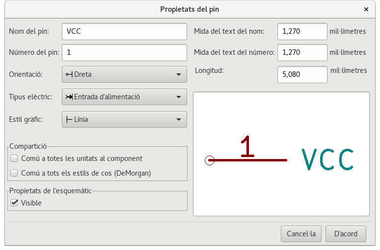
In the Pin Properties window that appears, set the pin name to 'VCC', set the pin number to '1', and the 'Electrical type' to 'Power input' then click OK.
-
Col·loqueu el pin en fer clic a la ubicació on vulgueu que estigui, just sota l’etiqueta de «MYCONN3».
-
Repetiu els passos per a afegir el pin, aquest cop el «Nom del pin» ha de ser «INPUT», el «Número del pin» ha de ser «2», i el «Tipus elèctric» ha de ser «Passiu».
-
Repetiu els passos per a afegir el pin, aquest cop el «Nom del pin» ha de ser «GND», el «Número del pin» ha de ser «3» i el «Tipus elèctric» ha de ser «Passiu». Col·loqueu els pins un a damunt de l’altre. L’etiqueta del component «MYCONN3» ha d’estar al centre de la pàgina (on es creuen les línies blaves).
-
A continuació, traceu el contorn del component. Feu clic a la icona «Afegeix un rectangle»
 . Volem traçar un rectangle a prop dels pins, com es mostra a continuació. Per a fer-ho, feu clic on vulgueu que estigui la cantonada superior esquerra del rectangle (no mantingueu premut el botó del ratolí). Feu clic de nou on vulgueu que estigui la cantonada inferior dreta del rectangle.
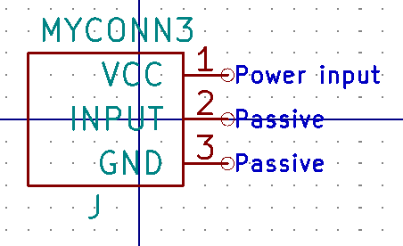
-
If you want to fill the rectangle with yellow, set the fill colour to 'yellow 4' in Preferences → Select color scheme, then select the rectangle in the editing screen with [e], selecting 'Fill background'.
-
Deseu el component a la vostra biblioteca myLib.lib. Feu clic a la icona «Nova biblioteca»
 , navegueu a la carpeta tutorial1/library/ i deseu el fitxer de la biblioteca nova amb el nom myLib.lib.
 -
Aneu a Preferències → Biblioteques de components i afegiu el camí a la biblioteca tutorial1/library/ als «Camins de cerca definits de l’usuari» i la biblioteca myLib.lib als «Fitxers de biblioteques de components».
-
Feu clic a la icona «Selecciona la biblioteca de treball»
 . En la finestra Selecciona la biblioteca feu clic a myLib i deu clic a «D’acord». Denoteu com el títol de la finestra indica que la biblioteca està actualment en ús, que ara hauria de ser myLib.
 -
Feu clic a la icona «Actualitza el component actual a la biblioteca actual»
 de la barra d’eines superior. Deseu tots els canvis en fer clic a la icona «Desa la biblioteca actual al disc»
  de la barra d’eines superior. Feu clic a «Sí» en qualsevol dels missatges de confirmació que apareguin. Ara ja està fet el nou component de l’esquemàtic i està disponible a la biblioteca que indica a la barra de títol de la finestra.
 -
Ara podeu tancar la finestra de l’editor de biblioteques de components. Tornareu a la finestra de l’editor d’esquemàtics. El vostre component nou estarà disponible a la biblioteca myLib.
-
Podeu fer que qualsevol fitxer de biblioteca fitxer.lib estigui disponible en afegir-lo al camí a les biblioteques. Des d'Eeschema, aneu a Preferències → Biblioteques de components i afegiu-hi el camí als «Camins de cerca definits de l’usuari» i el fitxer.lib als «Fitxers de biblioteques de components».
Exportació, importació i modificació dels components de la biblioteca
En lloc de crear un component de biblioteca de zero a vegades és més fàcil de començar a partir d’un ja fet i modificar-lo. En aquesta secció veurem com exportar un component de la biblioteca estàndard «device» de KiCad a la vostra biblioteca myOwnLib.lib i després el modificarem.
-
Des de KiCad, inicieu Eeschema, feu clic a la icona «Editor de biblioteques»
, feu clic a la icona «Selecciona la biblioteca de treball» i seleccioneu la biblioteca «device». Feu clic a la icona «Carrega el component per a editar-lo des de la biblioteca actual»  i importeu «RELAY_2RT».
 -
Feu clic a la icona «Exporta el component»
 , navegueu a la carpeta library/ i deseu el fitxer de la biblioteca nova amb el nom myOwnLib.lib.
 -
You can make this component and the whole library myOwnLib.lib available to you by adding it to the library path. From Eeschema, go to Preferences → Component Libraries and add both library/ in 'User defined search path' and myOwnLib.lib in the 'Component library files'. Close the window.
-
Feu clic a la icona «Selecciona el directori de treball»
. En la finestra Seleccioneu la biblioteca feu clic a myOwnLib i feu clic a «D’acord». Denoteu com el títol de la finestra indica que la biblioteca està actualment en ús, hauria de ser myOwnLib. -
Feu clic a la icona «Carrega el component per editar-lo des de la biblioteca actual»
i importeu «RELAY_2RT». -
You can now modify the component as you like. Hover over the label 'RELAY_2RT', press [e] and rename it 'MY_RELAY_2RT'.
-
Feu clic a la icona «Actualitza el component actual a la biblioteca actual»
de la barra d’eines superior. Deseu tots els canvis en fer clic a la icona «Desa la biblioteca carregada actualment al disc» de la barra d’eines superior.
Creació de components esquemàtics amb quicklib
En aquesta secció es presenta una manera alternativa per a crear el component esquemàtic per a MYCONN3 (vegeu a sota MYCONN3) amb l’eina d’Internet quicklib.
-
Dirigiu-vos la pàgina web de quicklib: http://kicad.rohrbacher.net/quicklib.php
-
Ompliu la pàgina amb la següent informació: Component name: MYCONN3 Reference Prefix: J Pin Layout Style: SIL Pin Count, N: 3
-
Feu clic a la icona «Assign Pins». Ompliu la pàgina amb la següent informació: Pin 1: VCC Pin 2: input Pin 3: GND. Type : Passive for all 3 pins.
-
Feu clic a la icona «Preview it» i si us satisfà, feu clic a «Build Library Component». Baixeu el fitxer i reanomeneu-lo com a tutorial1/library/myQuickLib.lib.. Ja està fet!
-
Doneu-li un cop d’ull amb KiCad. Des del gestor del projecte de KiCad, inicieu Eeschema, feu clic a la icona de l'«Editor de biblioteques»
, feu clic a la icona «Importa un component»  , navegueu a la carpeta tutorial1/library/ i seleccioneu myQuickLib.lib.
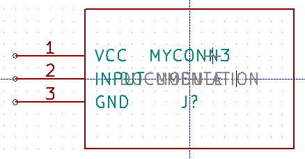
-
Podeu fer que aquest component i tota la biblioteca myQuickLib.lib estiguin disponibles si ho afegiu al camí de la biblioteca de KiCad. Des d'Eeschema, aneu a Preferències → Biblioteques de components i afegiu la biblioteca library al «Camí de cerca definit de l’usuari» i afegiu myQuickLib.lib als «Fitxers de biblioteques de components».
Com us podeu imaginar, aquest mètode de creació de components de biblioteques pot ser molt eficaç quan es vulguin crear components amb un gran nombre de pins.
Creació d’un component esquemàtic amb un nombre elevat de pins
En la secció que té per títol Creació de components esquemàtics amb quicklib vam veure com crear un component esquemàtic amb l’eina web quicklib. No obstant, de tant en tant us trobareu amb la necessitat de crear un component esquemàtic amb un nombre elevat de pins (alguns centenars de pins). En KiCad, aquesta no és una tasca molt complicada.
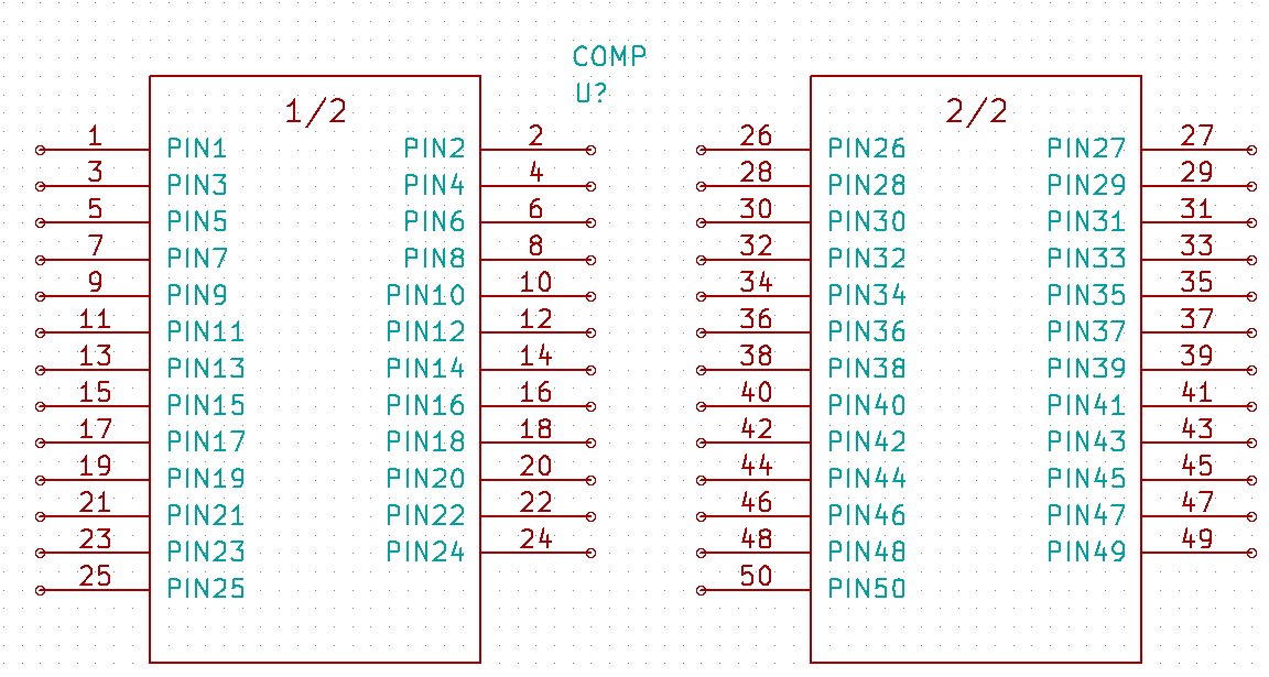
-
Suposem que volem crear un component esquemàtic per a un dispositiu amb 50 pins. És una pràctica comuna traçar-ho amb diversos dibuixos amb un nombre baix de pins, per exemple, dos dibuixos amb 25 pins cadascun. Aquesta representació del component permet una connexió fàcil dels pins.
-
La millor manera de crear el nostre component és utilitzar quicklib per a generar dos components separats de 25 pins, tornar a numerar els seus pins amb un script de Python i finalment fusionar-los mitjançant l’ús de copiar i enganxar per a crear un sol component DEF i ENDDEF.
-
Trobareu un exemple de script senzill de Python script a continuació, que es pot utilitzar en conjunció amb un fitxer in.txt i un fitxer out.txt per a tornar a numerar la línia: «X PIN1 1 -750 600 300 R 50 50 1 1 I» a «X PIN26 26 -750 600 300 R 50 50 1 1 I », això es fa per a totes les línies del fitxer in.txt.
Script senzill
#!/usr/bin/env python
''' simple script to manipulate KiCad component pins numbering'''
import sys, re
try:
    fin=open(sys.argv[1],'r')
    fout=open(sys.argv[2],'w')
except:
    print "oh, wrong use of this app, try:", sys.argv[0], "in.txt out.txt"
    sys.exit()
for ln in fin.readlines():
    obj=re.search("(X PIN)(\d*)(\s)(\d*)(\s.*)",ln)
if obj:
    num = int(obj.group(2))+25
    ln=obj.group(1) + str(num) + obj.group(3) + str(num) + obj.group(5) +'\n'
    fout.write(ln)
fin.close(); fout.close()
#
# for more info about regular expression syntax and KiCad component generation:
# http://gskinner.com/RegExr/
# http://kicad.rohrbacher.net/quicklib.php-
Mentre realitzeu la fusió dels dos components en un de sol, cal utilitzar l’Editor de biblioteques des d’Eeschema per a moure el primer component, ja que el segon no acaba a la part superior d’aquest. A continuació trobareu el fitxer final .lib i la seva representació a Eeschema.
Els continguts d’un fitxer *.lib
EESchema-LIBRARY Version 2.3
#encoding utf-8
# COMP
DEF COMP U 0 40 Y Y 1 F N
F0 "U" -1800 -100 50 H V C CNN
F1 "COMP" -1800 100 50 H V C CNN
DRAW
S -2250 -800 -1350 800 0 0 0 N
S -450 -800 450 800 0 0 0 N
X PIN1 1 -2550 600 300 R 50 50 1 1 I

...

X PIN49 49 750 -500 300 L 50 50 1 1 I
ENDDRAW
ENDDEF
#End Library
-
El script de Python que es presenta aquí és una eina molt potent per manipular tant els números dels pins com les etiquetes dels pins. Tingueu present que tot el seu poder prové de la sintaxi de les expressions regulars i no obstant això és increïblement útil http://gskinner.com/RegExr/.
Creació de les empremtes dels components
Unlike other EDA software tools, which have one type of library that contains both the schematic symbol and the footprint variations, KiCad .lib files contain schematic symbols and .kicad_mod files contain footprints. Cvpcb is used to map footprints to symbols.
Pel que fa als fitxers .lib files, els fitxers de les biblioteques .kicad_mod són fitxers de text que poden contenir una a diverses peces.
Hi ha una biblioteca de components extensa amb KiCad, malgrat això, de vegades us podeu trobar que l’empremta que necessiteu no està a la biblioteca de KiCad. Aquests són els passos per a la creació d’una nova empremta de placa de circuit imprès en KiCad:
Ús de l’editor d’empremtes
-
Des del gestor del projecte inicieu l’eina Pcbnew. Feu clic a la icona «Obre l’editor d’empremtes»
 de la barra d’eines superior. Això obrirà l'«Editor d’empremtes».
 -
We are going to save the new footprint 'MYCONN3' in the new footprint library 'myfootprint'. Create a new folder myfootprint.pretty in the tutorial1/ project folder. Click on the Preferences → Footprint Libraries Manager and press 'Append Library' button. In the table, enter "myfootprint" as Nickname, enter "${KIPRJMOD}/myfootprint.pretty" as Library Path and enter "KiCad" as Plugin Type. Press OK to close the PCB Library Tables window. Click on the 'Select active library' icon
 on the top toolbar. Select the 'myfootprint' library.
 -
Feu clic a la icona «Nova empremta»
 de la barra d’eines superior. Teclegeu «MYCONN3» com a «nom de l’empremta». Al mig de la pantalla apareixerà l’etiqueta «MYCONN3». Sota l’etiqueta podreu veure l’etiqueta «REF*». Feu clic secundari a «MYCONN3» i moveu a sobre de «REF*». Feu clic secundari a «REF*__», seleccioneu «Edita el text» ai reanomeneu-ho a «SMD». Establiu el valor de «Pantalla» a «Invisible».
 -
Select the 'Add Pads' icon
 on the right toolbar. Click on the working sheet to place the pad. Right click on the new pad and click 'Edit Pad'. You can also use [e].
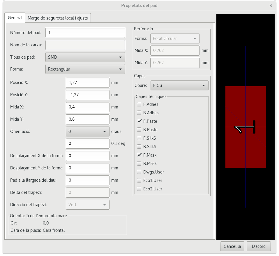
-
Establiu el «Número del pad» a «1», «Forma» a «Rectangular», «Tipus de pad» a «SMD», «Mida X» a «0,4», i «Mida Y» a «0,8». Feu clic a «D’acord». Feu clic un altre cop a «Afegeix pads» i col·loqueu dos pads més.
-
Si voleu canviar la mida de la quadrícula, Clic secundari → Selecció de la quadrícula. Assegureu-vos que seleccioneu la mida de la quadrícula corresponent abans que s’estableixen els components.
-
Moveu les etiquetes «MYCONN3» i «SMD» perquè es vegin com a la imatge de mostra.
-
Quan es col·loquen els pads de vegades és necessari calcular les distàncies relatives. Col·loqueu el cursor allí on vulgueu un punt_(0,0)_ de coordenada relativa i premeu la barra d’espai. Mentre es mou el cursor, a la part inferior de la pàgina veureu una indicació de la posició relativa del cursor. Premeu la barra d’espai en qualsevol moment per establir el nou origen.
-
Ara afegiu un contorn a l’empremta. Feu clic al botó «Afegeix una línia gràfica o un polígon gràfic»
 de la barra d’eines de la dreta. Traceu la línia de delimitació al voltant del component.
 -
Feu clic a la icona «Desa l’empremta a la biblioteca activa»
de la barra d’eines superior, utilitzeu el nom predeterminat MYCONN3.
Nota sobre la portabilitat dels fitxers dels projectes de KiCad
Quins són els fitxers que heu d’enviar a algú perquè pugui carregar i utilitzar plenament el vostre projecte de KiCad?
Quan heu de compartir amb algú un projecte de KiCad, és important que el fitxer de l’esquemàtic .sch, el fitxer de la placa .kicad_pcb, el fitxer del projecte .pro i el fitxer netlist .net, s’enviïn juntament amb el fitxer de les peces de l’esquemàtic .lib i el fitxer de les empremtes .kicad_mod. Només d’aquesta manera la gent tindrà tota la llibertat per a modificar l’esquema i la placa.
Amb els esquemàtics de KiCad, la gent necessita els fitxers .lib que contenen els símbols. Aquests fitxers de biblioteca ha de carregar-se a les preferències d'Eeschema. D’altra banda, amb les plaques (els fitxers .kicad_pcb) i les empremtes es poden desar dins del fitxer .kicad_pcb. Podeu enviar a algú el fitxer .kicad_pcb i res més, encarà podrà observar i editar la placa. Però quan vulgui carregar els components des d’un netlist, es necessita que les biblioteques de les empremtes (.kicad_mod files) estiguin presents i es carreguin a les preferències de Pcbnew de la mateixa manera que per als esquemàtics. També és necessari carregar els fitxers .kicad_mod a les preferències de Pcbnew a fi que es mostrin aquestes empremtes a Cvpcb.
Si algú us envia un fitxer .kicad_pcb amb les empremtes que us agradaria utilitzar en una altra placa, podeu obrir l’editor d’empremtes, carregar una empremta des de la placa actual, i desar o exportar-ho a una altra biblioteca d’empremtes. També podeu exportar d’un sol cop totes les empremtes des d’un fitxer .kicad_pcb a través de Pcbnew → Fitxer → Arxiva → Empremtes → Crea un arxiu d’empremtes, això crearà un nou fitxer .kicad_mod amb totes les empremtes de la placa.
En poques paraules, si el PCB és l’únic que es vol distribuir, llavors amb el fitxer de la placa .kicad_pcb n’hi ha prou. No obstant això, si es vol proporcionar la plena capacitat per utilitzar i modificar l’esquemàtic, els seus components i el PCB, es recomana que es construeixi el zip i s’enviï el següent directori del projecte:
tutorial1/
|— tutorial1.pro
|— tutorial1.sch
|— tutorial1.kicad_pcb
|— tutorial1.net
|— library/
|   |— myLib.lib
|   |— myOwnLib.lib
|   \— myQuickLib.lib
|
|— myfootprint.pretty/
|   \— MYCONN3.kicad_mod
|
\— gerber/
    |— ...
    \— ...
Més informació sobre la documentació de KiCad
Aquesta ha estat una guia ràpida per a la majoria de les característiques en KiCad. Per a obtenir instruccions més detallades, consulteu els fitxers d’ajuda els quals es poden accedir a través de cadascun dels mòduls de KiCad. Fer clic a Ajuda → Manual.
KiCad inclou un bon recull de manuals que estan disponibles en diversos idiomes per a tots els seus quatre components de programari.
La versió anglesa de tots els manuals de KiCad es distribueixen amb KiCad.
A part dels manuals, KiCad es distribueix amb aquesta guia d’aprenentatge, la qual ha estat traduïda a altres idiomes. Totes les versions d’aquesta guia d’aprenentatge es distribueixen de forma gratuïta en totes les versions recents de KiCad. Aquesta guia d’aprenentatge, així com els manuals, han d’estar empaquetats amb la vostra versió de KiCad en la vostra plataforma específica.
Per exemple, en Linux les ubicacions típiques es troben en els següents directoris, segons quina sigui la distribució:
/usr/share/doc/kicad/help/en/
/usr/local/share/doc/kicad/help/en
En Windows està a:
<directori d'instal·lació>/share/doc/kicad/help/en
En OS X:
/Library/Application Support/kicad/help/en
Documentació de KiCad al web
The latest version of KiCad documentation can be found in multiple languages at http://docs.kicad.org