Reference manual
| This manual is in the process of being revised to cover the latest stable release version of KiCad. It contains some sections that have not yet been completed. We ask for your patience while our volunteer technical writers work on this task, and we welcome new contributors who would like to help make KiCad’s documentation better than ever. |
Copyright
This document is Copyright © 2010-2024 by its contributors as listed below. You may distribute it and/or modify it under the terms of either the GNU General Public License (http://www.gnu.org/licenses/gpl.html), version 3 or later, or the Creative Commons Attribution License (http://creativecommons.org/licenses/by/3.0/), version 3.0 or later.
All trademarks within this guide belong to their legitimate owners.
Contributors
Jean-Pierre Charras, Fabrizio Tappero, Wayne Stambaugh, Graham Keeth
Feedback
The KiCad project welcomes feedback, bug reports, and suggestions related to the software or its documentation. For more information on how to sumbit feedback or report an issue, please see the instructions at https://www.kicad.org/help/report-an-issue/
Introduction to the KiCad Schematic Editor
Description
The KiCad Schematic Editor is a schematic capture software distributed as a part of KiCad and available under the following operating systems:
-
Linux
-
Apple macOS
-
Windows
Regardless of the OS, all KiCad files are 100% compatible from one OS to another.
The Schematic Editor is an integrated application where all functions of drawing, control, layout, library management and access to the PCB design software are carried out within the editor itself.
The KiCad Schematic Editor is intended to cooperate with the KiCad PCB Editor, which is KiCad’s printed circuit design software. It can also export netlist files, which lists all the electrical connections, for other packages.
The Schematic Editor includes a symbol library editor, which can create and edit symbols and manage libraries. It also integrates the following additional but essential functions needed for modern schematic capture software:
-
Electrical rules check (ERC) for the automatic control of incorrect and missing connections
-
Export of plot files in many formats (Postscript, PDF, HPGL, and SVG)
-
Bill of Materials generation (via Python or XSLT scripts, which allow many flexible formats).
The Schematic Editor supports multi-sheet schematics in several ways:
-
Flat hierarchies (schematic sheets are not explicitly connected in a master diagram).
-
Simple hierarchies (each schematic sheet is used only once).
-
Complex hierarchies (some schematic sheets are used multiple times).
Hierarchical schematics are described in detail later in the manual.
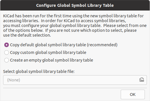
Initial Configuration
When the Schematic Editor is run for the first time, if the the global symbol
library table file sym-lib-table is not found in the KiCad configuration
folder then KiCad will ask how to create this file:
The first option is recommended (Copy default global symbol library table (recommended)). The default symbol library table includes all of the standard symbol libraries that are installed as part of KiCad.
If this option is disabled, KiCad was unable to find the default global symbol library table. This probably means you did not install the standard symbol libraries with KiCad, or they are not installed where KiCad expects to find them. On some systems the KiCad libraries are installed as a separate package.
-
If you have installed the standard KiCad symbol libraries and want to use them, but the first option is disabled, select the second option and browse to the
sym-lib-tablefile in the directory where the KiCad libraries were installed. -
If you already have a custom symbol library table that you would like to use, select the second option and browse to your
sym-lib-tablefile. -
If you want to construct a new symbol library table from scratch, select the third option.
Symbol library management is described in more detail later.
The Schematic Editor User Interface
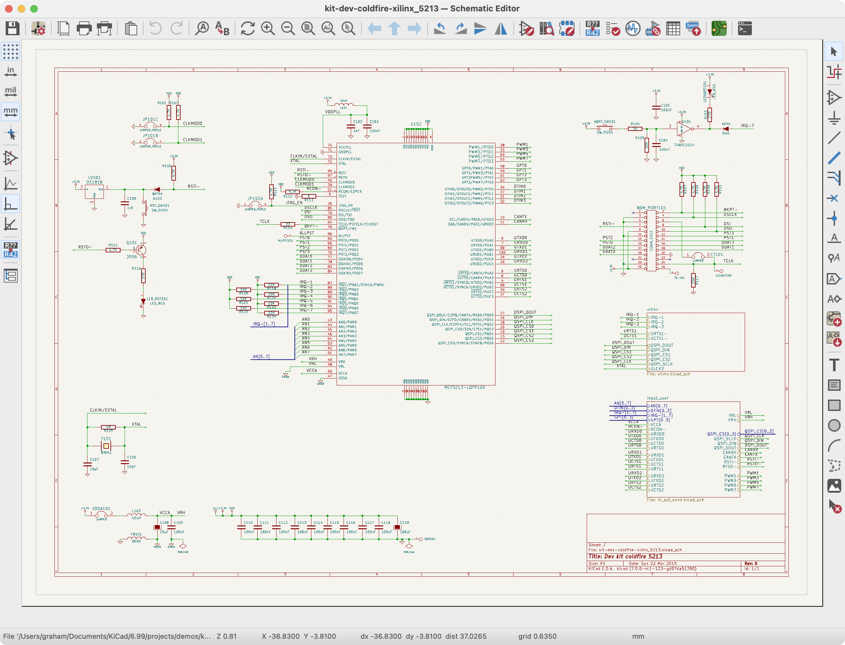
The main Schematic Editor user interface is shown above. The center contains the main editing canvas, which is surrounded by:
-
Top toolbars (file management, zoom tools, editing tools)
-
Left toolbar (display options)
-
Message panel and status bar at bottom
-
Right panel (drawing and design tools)
Navigating the editing canvas
The editing canvas displays the schematic being designed. You can pan and zoom to different parts of the schematic and open any schematic sheet in the design.
By default, dragging with the middle or right mouse button will pan the canvas view and scrolling the mouse wheel will zoom the view in or out. You can change this behavior in the Mouse and Touchpad section of the preferences (see Configuration and Customization for details).
Several other zoom tools are available in the top toolbar:
-
 zooms in on the center of the
viewport.
zooms in on the center of the
viewport. -
 zooms out from the center of
the viewport.
zooms out from the center of
the viewport. -
 zooms to fit the
frame around the drawing sheet.
zooms to fit the
frame around the drawing sheet. -
 zooms to
fit every item in the schematic (not including the drawing sheet). For
instance, if there are items placed outside of the drawing sheet, they will be
visible after zooming to objects.
zooms to
fit every item in the schematic (not including the drawing sheet). For
instance, if there are items placed outside of the drawing sheet, they will be
visible after zooming to objects. -
 allows you to
draw a box to determine the zoomed area.
allows you to
draw a box to determine the zoomed area.
The cursor’s current position is displayed at the bottom of the window (X and Y), along with the current zoom factor (Z), the cursor’s relative position (dx, dy, and dist), the grid setting, and the display units.
The relative coordinates can be reset to zero by pressing Space. This is useful for measuring distance between two points or aligning objects.
Hotkeys
The Ctrl+F1 shortcut displays the current hotkey list. The default hotkey list is included in the Actions Reference section of the manual.
The hotkeys described in this manual use the key labels that appear on a standard PC keyboard. On an Apple keyboard layout, use the Cmd key in place of Ctrl, and the Option key in place of Alt.
Many actions do not have hotkeys assigned by default, but hotkeys can be assigned or redefined using the hotkey editor (Preferences → Preferences… → Hotkeys).
| Many of the actions available through hotkeys are also available in context menus. To access the context menu, right-click in the editing canvas. Different actions will be available depending on what is selected or what tool is active. |
Hotkeys are stored in the file user.hotkeys in KiCad’s configuration
directory. The location is platform-specific:
-
Windows:
%APPDATA%\kicad\7.0\user.hotkeys -
Linux:
~/.config/kicad/7.0/user.hotkeys -
macOS:
~/Library/Preferences/kicad/7.0/user.hotkeys
KiCad can import hotkey settings from a user.hotkeys file using the Import
Hotkeys button in the hotkey editor.
Mouse operations and selection
Selecting items in the editing canvas is done with the left mouse button. Single-clicking on an object will select it. Clicking and dragging will perform a box selection. A box selection from left to right will only select items that are fully inside the box. A box selection from right to left will select any items that touch the box. A left-to-right selection box is drawn in yellow, with a cursor that indicates exclusive selection, and a right-to-left selection box is drawn in blue with a cursor that indicates inclusive selection.
The selection action can be modified by holding modifier keys while clicking or dragging. The following modifier keys apply when clicking to select single items:
| Modifier Keys (Windows) | Modifier Keys (Linux) | Modifier Keys (macOS) | Selection Effect |
|---|---|---|---|
Ctrl |
Ctrl |
Cmd |
Toggle selection. |
Shift |
Shift |
Shift |
Add the item to the existing selection. |
Ctrl+Shift |
Ctrl+Shift |
Cmd+Shift |
Remove the item from the existing selection. |
long click |
long click or Alt |
long click or Option |
Clarify selection from a pop-up menu. |
The following modifier keys apply when dragging to perform a box selection:
| Modifier Keys (Windows) | Modifier Keys (Linux) | Modifier Keys (macOS) | Selection Effect |
|---|---|---|---|
Ctrl |
Ctrl |
Cmd |
Toggle selection. |
Shift |
Shift |
Shift |
Add item(s) to the existing selection. |
Ctrl+Shift |
Ctrl+Shift |
Cmd+Shift |
Remove item(s) from the existing selection. |
Selecting an object displays information about the object in the message panel at the bottom of the window. Double-clicking an object opens a window to edit the object’s properties.
Pressing Esc will always cancel the current tool or operation and return to the selection tool. Pressing Esc while the selection tool is active will clear the current selection.
Left toolbar display controls
The left toolbar provides options to change the display of items in the Schematic Editor.
|
Turns grid display on/off. Note: by default, hiding the grid will disable grid snapping. This behavior can be changed in the Display Options section of Preferences. |
|
Display/entry of coordinates and dimensions in inches, mils, or millimeters. |
|
Switches between full-screen and small editing cursor (crosshairs). |
|
Turns invisible pin display on/off. |
|
Switches between free angle, 90 degree mode, and 45 degree mode for placement of new wires, buses, and graphical lines. |
|
Opens and closes the docked hierarchy navigator pane. |
Schematic Creation and Editing
Introduction
A schematic designed with KiCad is more than a simple graphic representation of an electronic device. It is normally the entry point of a development chain that allows for:
-
Validating against a set of rules (Electrical Rules Check) to detect errors and omissions.
-
Automatically generating a bill of materials.
-
Generating a netlist for simulation software such as SPICE.
-
Defining a circuit for transferring to PCB layout.
A schematic mainly consists of symbols, wires, labels, junctions, buses and power symbols. For clarity in the schematic, you can place purely graphical elements like bus entries, comments, and polylines.
Symbols are added to the schematic from symbol libraries. After the schematic is made, the set of connections and footprints is imported into the PCB editor for designing a board.
Schematics can be contained in a single sheet or split among multiple sheets. In
KiCad, multi-sheet schematics are organized hierarchically, with a root sheet
and sub-sheet(s). Each sheet is its own .kicad_sch file and is itself a
complete KiCad schematic. Working with hierarchical schematics is described in
the Hierarchical Schematics chapter.
Schematic editing operations
Schematic editing tools are located in the right toolbar. When a tool is activated, it stays active until a different tool is selected or the tool is canceled with the Esc key. The selection tool is always activated when any other tool is canceled.
|
Selection tool (the default tool) |
|
Highlight a net by marking its wires and net labels with a different color. If the PCB Editor is also open then copper corresponding to the selected net will be highlighted as well. Net highlighting can be cleared by clicking with the highlight tool in an empty space, or by using the Clear Net Highlighting hotkey (~). |
|
Display the symbol selector dialog to place a new symbol. |
|
Display the power symbol selector dialog to place a new power symbol. |
|
Draw a wire. |
|
Draw a bus. |
|
Draw wire-to-bus entry points. These elements are only graphical and do not create a connection, thus they should not be used to connect wires together. |
|
Place a "no-connection" flag. These flags should be placed on symbol pins which are meant to be left unconnected. "No-connection" flags indicate to the Electrical Rule Checker that the pin is intentionally unconnected and not an error. |
|
Place a junction. This connects two crossing wires or a wire and a pin, which can sometimes be ambiguous without a junction (i.e. if a wire end or a pin is not directly connected to another wire end). |
|
Place a local label. Local labels connect items located in the same sheet. For connections between two different sheets, use global or hierarchical labels. |
|
Place a net class directive label. |
|
Place a global label. All global labels with the same name are connected, even when located on different sheets. |
|
Place a hierarchical label. Hierarchical labels are used to create a connection between a subsheet and the sheet’s parent sheet. See the Hierarchical Schematics section for more information about hierarchical labels, sheets, and pins. |
|
Place a hierarchical subsheet. You must specify the file name for this subsheet. |
|
Import a hierarchical pin from a subsheet. This command can be executed only on hierarchical subsheets. It will create hierarchical pins corresponding to hierarchical labels placed in the target subsheet. |
|
Place a text comment. |
|
Place a text box. |
|
Draw a rectangle. |
|
Draw a circle. |
|
Draw an arc. |
|
Draw lines. Note: Lines are graphical objects and are not the same as wires placed with the Wire tool. They do not connect anything. |
|
Place a bitmap image. |
|
Delete clicked items. |
Grids
In the Schematic Editor the cursor always moves over a grid. The grid can be customized:
-
Size can be changed using the right click menu or using View → Grid Properties….
-
Color can be changed in the Colors page of the Preferences dialog (menu Preferences → General Options).
-
Visibility can be switched using the left-hand toolbar button.
The default grid size is 50 mil (0.050") or 1.27 millimeters.
This is the recommended grid for placing symbols and wires in a schematic, and for placing pins when designing a symbol in the Symbol Editor.
| Wires connect with other wires or pins only if their ends coincide exactly. Therefore it is very important to keep symbol pins and wires aligned to the grid. It is recommended to always use a 50 mil grid when placing symbols and drawing wires because the KiCad standard symbol library and all libraries that follow its style also use a 50 mil grid. Using a grid size other than 50 mil will result in schematics without proper connectivity! |
Smaller grids can also be used, but this is intended only for text and symbol graphics, and not recommended for placing pins and wires.
| Symbols, wires, and other elements that are not aligned to the grid can be snapped back to the grid by selecting them, right clicking, and clicking Align Elements to Grid. |
Snapping
Schematic elements such as symbols, wires, text, and graphic lines are snapped to the grid when moving, dragging, and drawing them. Additionally, the wire tool snaps to pins even when grid snapping is disabled. Both grid and pin snapping can be disabled while moving the mouse by using the modifier keys in the table below.
| On Apple keyboards, use the Cmd key instead of Ctrl. |
| Modifier Key | Effect |
|---|---|
Ctrl |
Disable grid snapping. |
Shift |
Disable snapping wires to pins. |
Editing object properties
All objects have properties that are editable in a dialog. Use the hotkey E or select Properties from the right-click context menu to edit the properties of selected item(s). You can only open the properties dialog if all the items you have selected are of the same type. To edit the properties of different types of items at one time, see the section below on bulk editing tools.
In properties dialogs, any field that contains a numeric value can also accept a
basic math expression that results in a numeric value. For example, a dimension
may be entered as 2 * 2mm, resulting in a value of 4mm. Basic arithmetic
operators as well as parentheses for defining order of operations are supported.
Working with symbols
Placing symbols
To place a symbol in your schematic, use the
![]() button or the A
hotkey. The Choose Symbols dialog appears and lets you select a symbol to add.
Symbols are grouped by symbol library.
button or the A
hotkey. The Choose Symbols dialog appears and lets you select a symbol to add.
Symbols are grouped by symbol library.
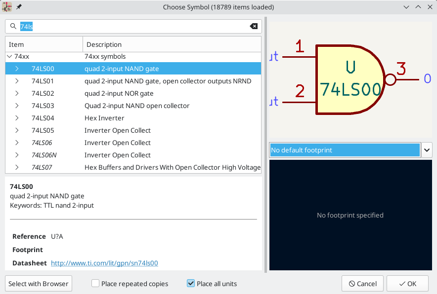
By default, only the symbol/library name and description columns are shown. Additional columns can be added by right-clicking the column header and selecting Select Columns.
The Choose Symbol dialog filters symbols by name, keywords, description, and all additional symbol fields according to what you type into the search field.
Some advanced filters are available:
-
Wildcards:
*matches any number of any characters, including none, and?matches any single character. -
Key-value pairs: if a library part’s description or keywords contain a tag of the format "Key:123", you can match relative to that by typing "Key>123" (greater than), "Key<123" (less than), etc. Numbers may include one of the following case-insensitive suffixes:
p
n
u
m
k
meg
g
t
10-12
10-9
10-6
10-3
103
106
109
1012
ki
mi
gi
ti
210
220
230
240
-
Regular expressions: if you’re familiar with regular expressions, these can be used too. The regular expression flavor used is the wxWidgets Advanced Regular Expression style, which is similar to Perl regular expressions.
If the symbol specifies a default footprint, this footprint will be previewed in the lower right. If the symbol includes footprint filters, alternate footprints that satisfy the footprint filters can be selected in the footprint dropdown menu at right.
After selecting a symbol to place, the symbol will be attached to the cursor. Left clicking the desired location in the schematic places the symbol into the schematic. Before placing the symbol in the schematic, you can rotate it, mirror it, and edit its fields, by either using the hotkeys or the right-click context menu. These actions can also be performed after placement.
If the Place repeated copies option is checked, after placing a symbol KiCad will start placing another copy of the symbol. This process continues until the user presses Esc.
For symbols with multiple units, if the Place all units option is checked, after placing the symbol KiCad will start placing the next unit in the symbol. This continues until the last unit has been placed or the user presses Esc.
Placing power symbols
A power symbol is a symbol representing a connection to a
power net. The symbols are grouped in the power library, so they can be
placed using the symbol chooser. However, as power placements are frequent, the
![]() tool is available. This tool
is similar, except that the search is done directly in the
tool is available. This tool
is similar, except that the search is done directly in the power library and
any other library that contains power symbols.
Moving symbols
Symbols can be moved using the Move (M) or Drag (G) tools. These tools act on the selected symbol, or if no symbol is selected they act on the symbol under the cursor.
The Move tool moves the symbol itself without maintaining wired connections to the symbol pins.
The Drag tool moves the symbol without breaking wired connections to its pins, and therefore moves the connected wires as well.
You can also Drag symbols by clicking and dragging them with the mouse, depending on the Left button drag gesture setting in the Mouse and Touchpad section of Preferences.
Symbols can also be rotated (R) or mirrored in the X (X) or Y (Y) directions.
Editing symbol properties
A symbol’s fields can be edited in the symbol’s Properties window. Open the Symbol Properties window for a symbol with the E hotkey or by double-clicking on the symbol.
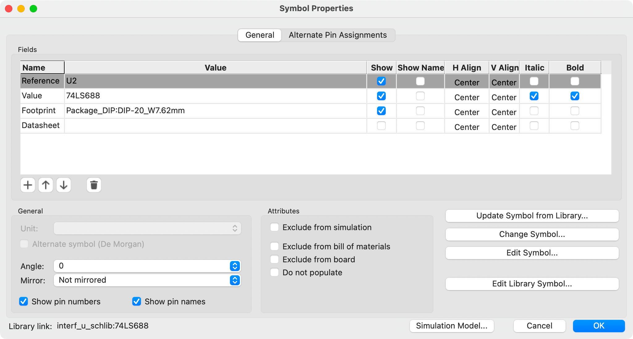
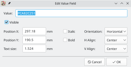
The Symbol Properties window displays all the fields of a symbol in a table. New fields can be added, and existing fields can be deleted, edited, reordered, moved, or resized.
Each field’s name and value can be visible or hidden, and there are several formatting options: horizontal and vertical alignment, orientation, position, font, text color, text size, and bold/italic emphasis. Field autoplacement can also be enabled on a per-field basis. The displayed position is always indicated for a normally displayed symbol (no rotation or mirroring) and is relative to the anchor point of the symbol.
| Formatting options for symbol fields can be shown or hidden by right-clicking on the header row of the symbol field table and enabling or disabling the desired columns. Not all columns are shown by default. |
The Update Symbol from Library… button is used to update the schematic’s copy of the symbol to match the copy in the library. The Change Symbol… button is used to swap the current symbol to a different symbol in the library. These functions are described later.
Edit Symbol… opens the Symbol Editor to edit the copy of the symbol in the schematic. Note that the original symbol in the library will not be modified. The Edit Library Symbol… button opens the Symbol Editor to edit the original symbol in the library. In this case, the symbol in the schematic will not be modified until the user clicks the Update Symbol from Library… button.
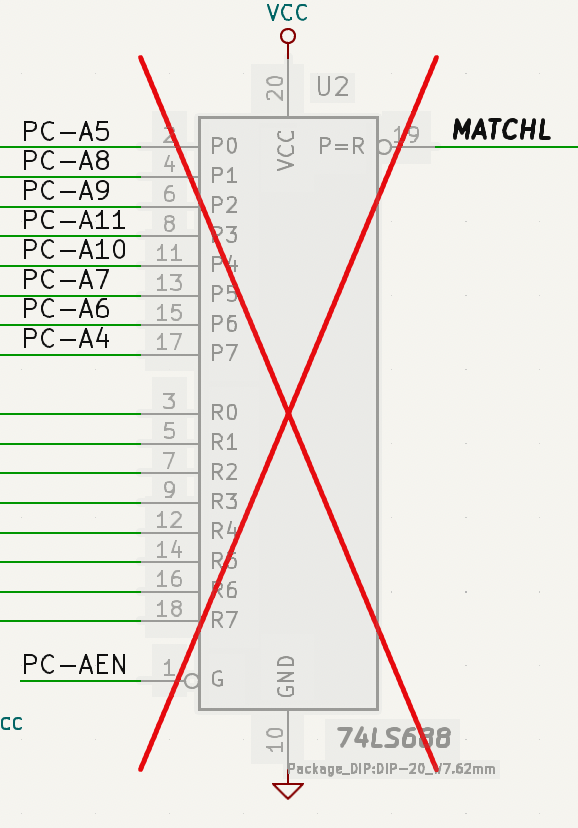
Symbols have several attributes that affect how the symbols are treated by other parts of KiCad.
Exclude from simulation prevents the symbol from being included in SPICE simulations.
Exclude from bill of materials prevents the component from being included in BOM exports.
Exclude from board means that the symbol is schematic-only, and a corresponding footprint will not be added to the PCB.
Do not populate means that the component should not be attached to the PCB, although a corresponding footprint should still be added to the board. DNP symbols appear desaturated and with a red "X" over them in the schematic, as shown below.
Editing symbol fields individually
An individual symbol text field can be edited directly with the E hotkey (with a field selected instead of a symbol) or by double-clicking on the field.
Some symbol fields have their own hotkey to edit them directly. With the symbol selected, the Reference, Value, and Footprint fields can be edited with the U, V, or F hotkeys, respectively.
The options in this dialog are the same as those in the full Symbol Properties dialog, but are specific to a single field.
Symbol fields can be automatically moved to an appropriate location with the Autoplace Fields action (select a symbol and press O). Field autoplacement is configurable in the Schematic Editor’s Editing Options, including a setting to always autoplace fields.
Updating and exchanging symbols
When a symbol is added to the schematic, KiCad embeds a copy of the library symbol in the schematic so that the schematic is independent of the system libraries. Symbols that have been added to the schematic are not automatically updated when the library changes. Library symbol changes are manually synced to the schematic so that the schematic does not change unexpectedly.
To update symbols in the schematic to match the corresponding symbol, use Tools → Update Symbols from Library, or right click a symbol and select Update Symbol from Library. You can also access the tool from the symbol properties dialog.
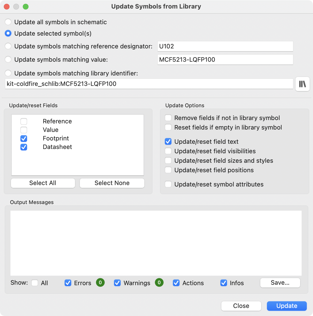
The top of the dialog has options to choose which symbols will be updated. You
can update all symbols in the dialog, update only the selected symbols, or
update only the symbols that match a specific reference designator, value, or
library identifier. The reference designator and value fields support wildcards:
* matches any number of any characters, including none, and ? matches any
single character.
The middle of the dialog has options to control what parts of the symbol will be updated. You can select specific fields to update or not update, which properties of the fields to update (text, visibility, size and style, and position), and how to handle fields that are missing or empty in the library symbol. You can also choose whether to update symbol attributes, such as do not populate and exclude from simulation / bill of materials / board.
The bottom of the dialog displays messages describing the update actions that have been performed.
To change an existing symbol to a different symbol, use Edit → Change Symbols…, or right click an existing symbol and select Change Symbol…. This dialog is also accessible from the symbol properties dialog.
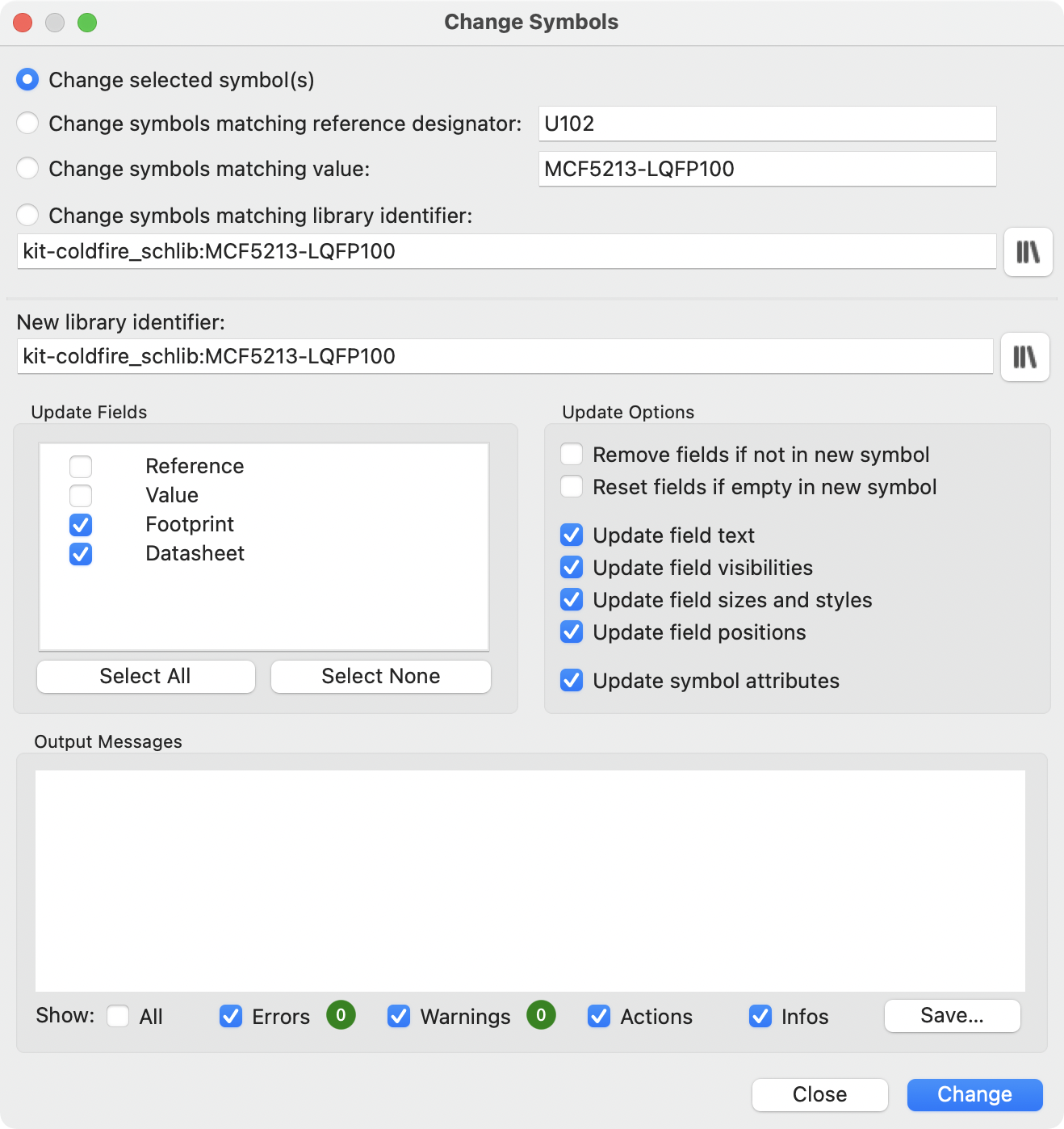
The options for the Change Symbols dialog are very similar to the Update Symbols from Library dialog.
Another way to swap existing symbols for new ones is to use Tools → Edit Symbol Library Links…. This dialog contains a table of every symbol in the design, grouped by current library symbol. By choosing a new symbol in the New Library Reference column, you can make all instances of the existing symbol instead point to the new symbol. If the Update symbol fields from new library option is used, the contents of the existing symbols' fields will be updated to match the new symbols' fields.
The Map Orphans button attempts to automatically remap orphaned symbols to
symbols with the same name in an active library. For example, if there is a symbol
with the current library reference mylib:symbol123, but the mylib library
cannot be found, the Map Orphans button will attempt to find a symbol named
symbol123 in any of the libraries that are present. This button is only
enabled if orphaned symbols are present in the schematic (see the
legacy schematics section).
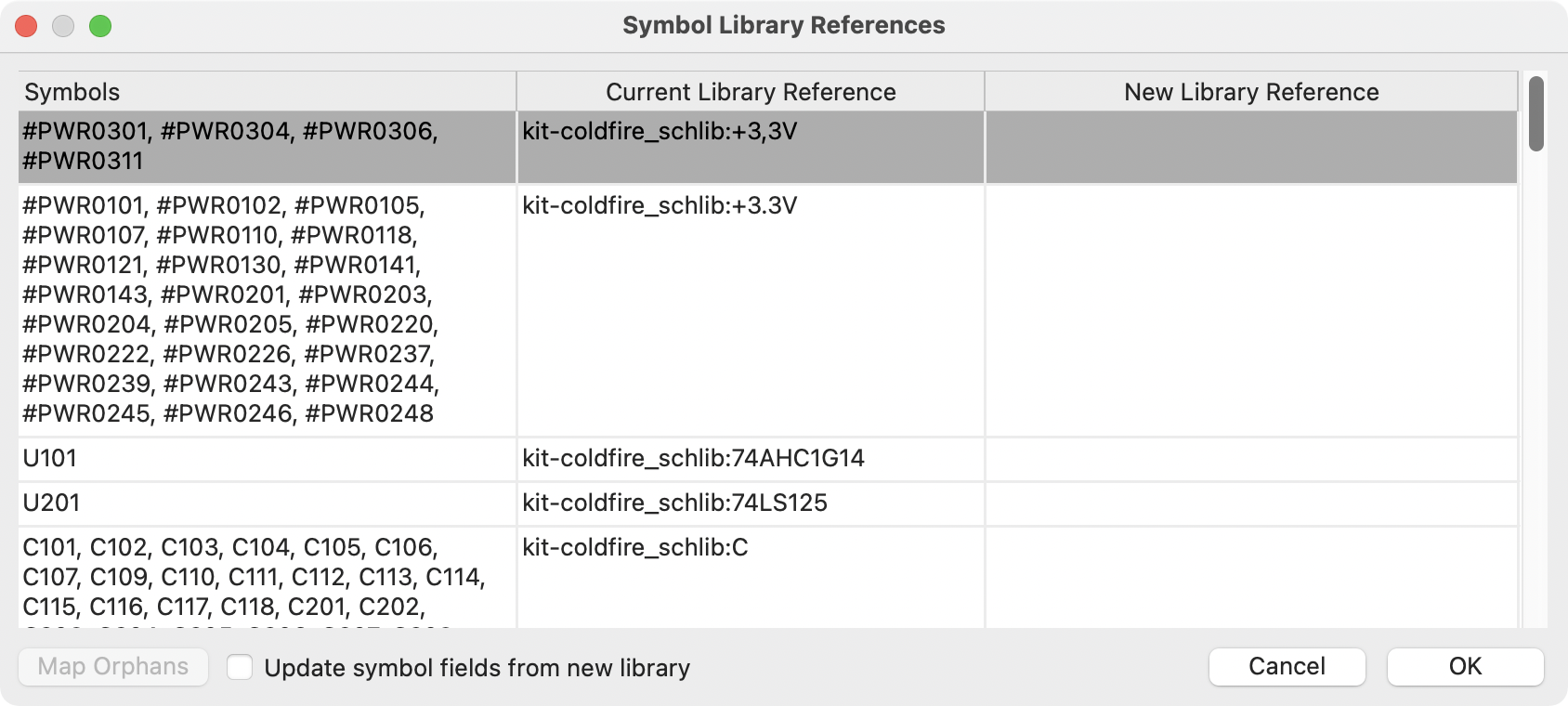
This dialog is primarily useful for managing symbols that appear in multiple libraries, when you want to switch from one library to another. For example, if a schematic uses symbols that are in both a global library and a project-specific library, the Symbol Library References dialog could be used to switch between using the global symbols or the equivalent project-specific symbols. It does not have features for fine-grained control of how fields are updated; for that, use the Change Symbols dialog.
Symbol Fields Table
The Symbol Fields Table allows you to view and modify field values for all
symbols in a spreadsheet interface. You can open the Symbol Fields Table with
the ![]() button.
button.
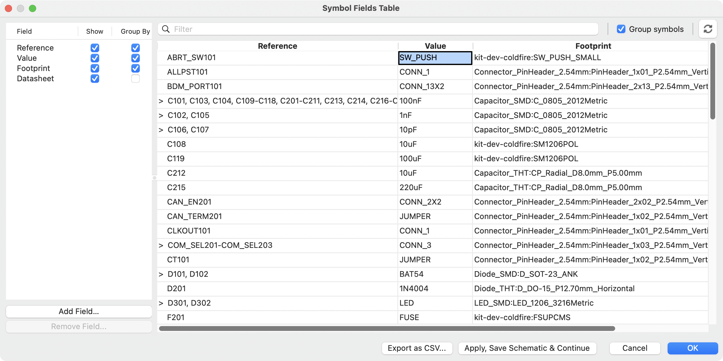
Cells are navigated with the arrow keys, or with Tab / Shift+Tab to move right / left and Enter / Shift+Enter to move down / up, respectively.
A range of cells can be selected by clicking and dragging. The whole range of selected cells will be copied (Ctrl+C) or pasted into (Ctrl+V) on a copy or paste action. Copying a range of cells from the table can be useful for creating a BOM. More details of copying and pasting cells are described below.
Any symbol field can be shown or hidden using the Show checkboxes on the left, or by right-clicking on the header of the table. New symbol fields can be added using the Add Field… button.
Similar symbols can optionally be grouped by any symbol field using the Group
By checkboxes. Grouped symbols are shown in a single row in the table. The
grouped row can be expanded to show the individual symbols by clicking the arrow
at the left of the row. The Group Symbols checkbox enables or disables
symbol grouping, and the ![]() button recalculates groupings.
button recalculates groupings.
Symbols can be filtered using the Filter textbox at the top. The filter
supports wildcards: * matches any number of any characters, including none,
and ? matches any single character.
You can use the Export as CSV… button to save the symbol fields to an external file. This can be used as a simple BOM generation tool, although the BOM tool provides better control over the generated output.
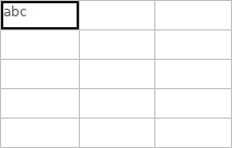
Tricks to simplify filling fields
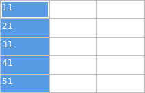
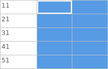
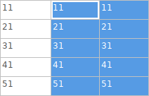
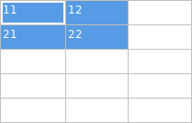
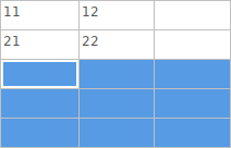
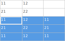
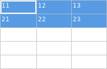
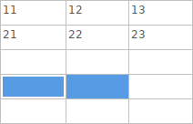
There are several special copy/paste methods in the spreadsheet for pasting values into larger regions, including auto-incrementing pasted cells. These features may be useful when pasting values that are shared in several symbols.
These methods are illustrated below.
| 1. Copy (Ctrl+C) | 2. Select target cells | 3. Paste (Ctrl+V) |
|---|---|---|
|
|
|
|
|
|
|
|
|
|
|
|
|
|
|
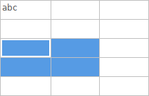
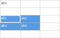
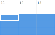
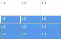
| These techniques are also available in other dialogs with a grid control element. |
Reference Designators and Symbol Annotation
Reference designators are unique identifiers for components in a design. They are often printed on a PCB and in assembly diagrams, and allow you to match symbols in a schematic to the corresponding components on a board.
In KiCad, reference designators consist of a letter indicating the type of
component (R for resistor, C for capacitor, U for IC, etc.) followed by a
number. If the symbol has multiple units then the reference designator will also
have a trailing letter indicating the unit. Symbols that don’t have a reference
designator set have a ? character instead of the number. Reference designators
must be unique.
Reference designators can be automatically set when symbols are added to the schematic, and you can set or reset reference designators yourself by manually editing an individual symbol’s reference designator field or in bulk using the Annotation tool.
| The process of setting a symbol’s reference designator is called annotation. |
Auto-annotation
When auto-annotation is enabled, symbols will be automatically annotated when
they are added to the schematic. You can enable auto-annotation by checking the
Automatically annotate symbols checkbox in the Schematic Editor →
Annotation Options pane in Preferences. Auto-annotation can also be
toggled using the ![]() button
in the left toolbar.
button
in the left toolbar.
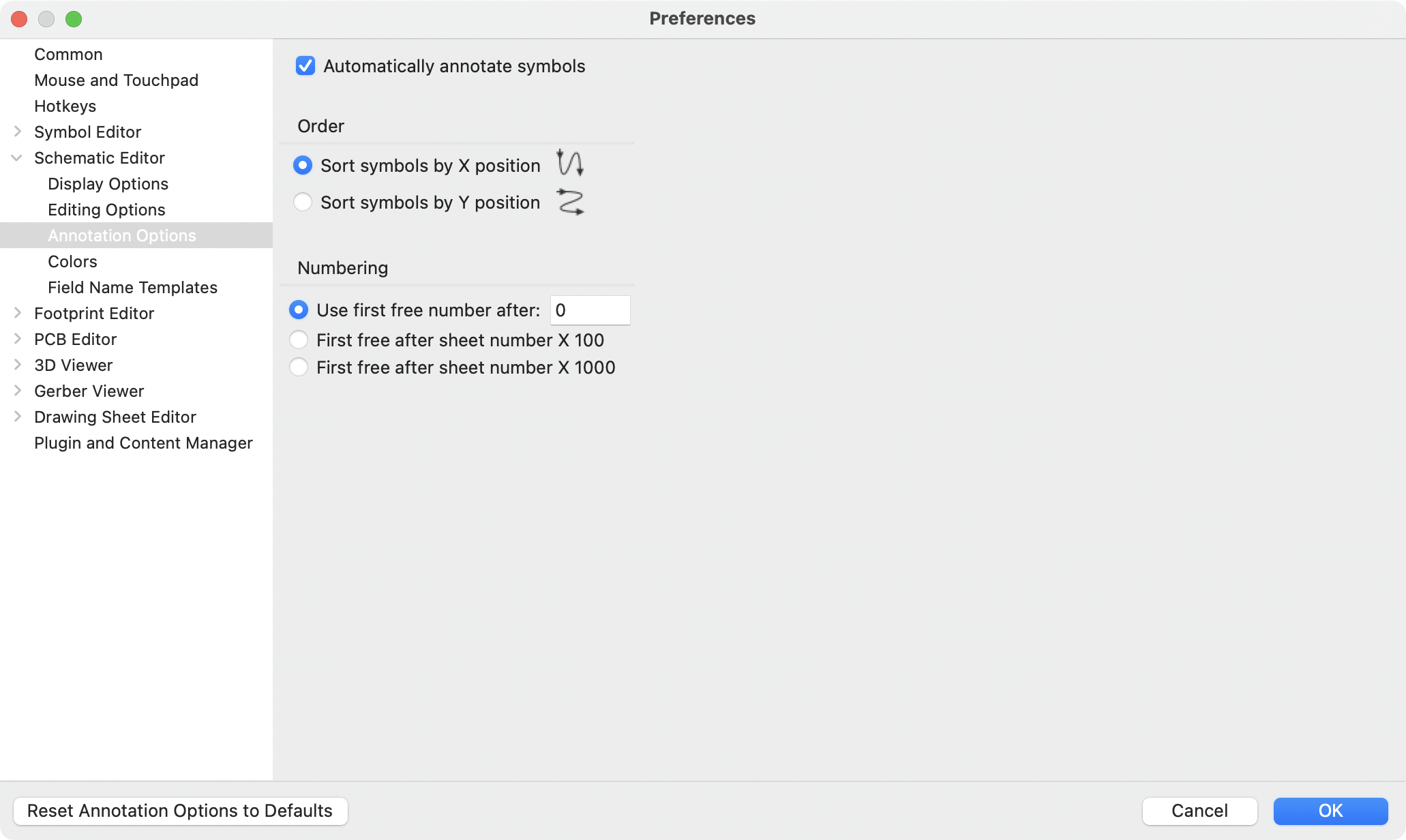
When multiple symbols are added simultaneously, they are annotated according to the Order setting, sorted by either X or Y position.
The Numbering option sets the starting number for new reference designators. This can be the lowest available number, or a number based on the sheet number.
For more information about annotation options, see the documentation for the Annotation tool.
Annotation tool
The Annotation tool automatically assigns reference designators to symbols in
the schematic. To launch the Annotation tool, click the
![]() button in the top toolbar.
button in the top toolbar.
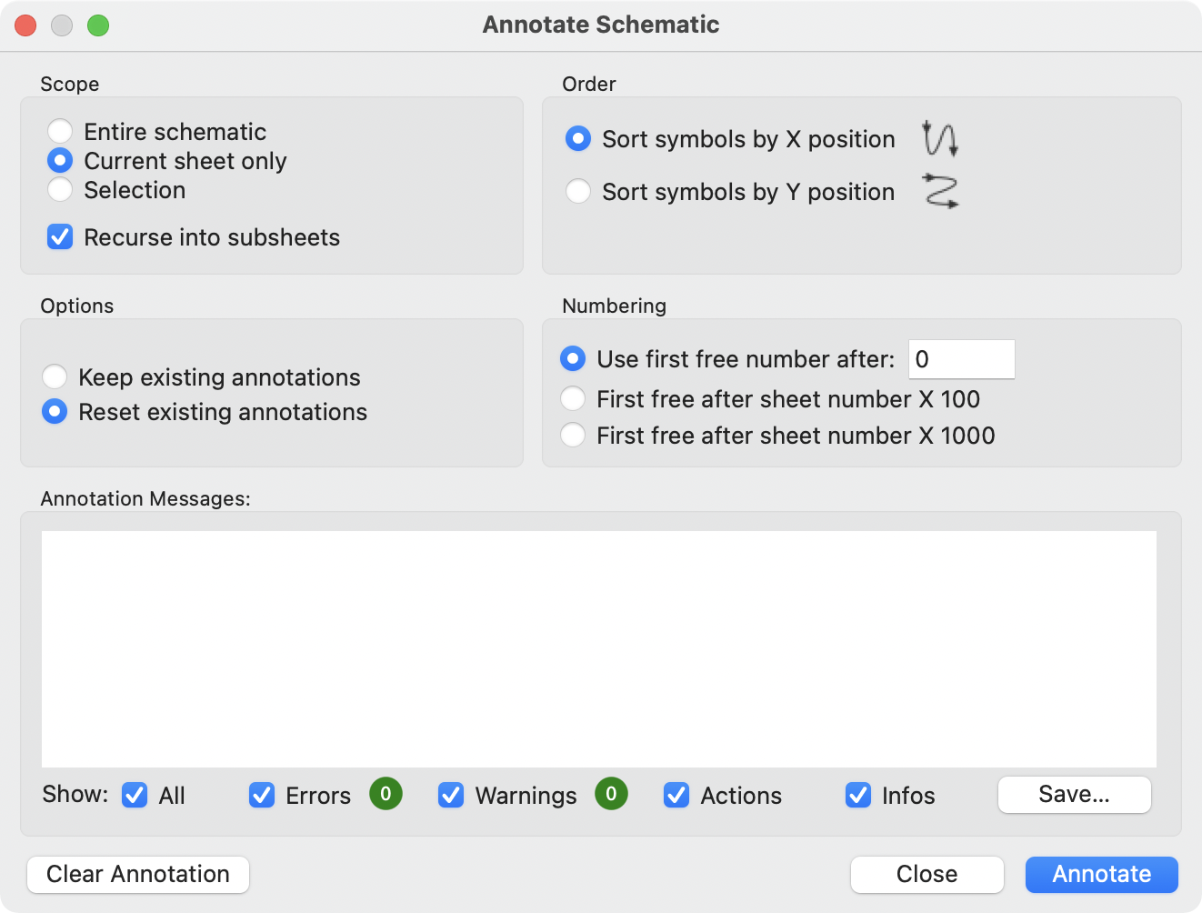
The tool provides several options to control how symbols are annotated.
Scope: Selects whether annotation is applied to the entire schematic, to only the current sheet, or to only the selected symbols. If the Recurse into subsheets option is selected, symbols in subsheets of the selected scope will be reannotated; otherwise symbols in subsheets will not be reannotated. For example, if Recurse into subsheets and Selection only selected, symbols in any selected subsheets will be reannotated.
Options: Selects whether annotation should apply to all symbols and reset *existing reference designators, or apply only to unannotated symbols.
Order: Chooses the direction of numbering. If symbols are sorted by X position, all symbols on the left side of a schematic sheet will be lower numbered than symbols on the right side of the sheet. If symbols are sorted by Y position, all symbols on the top of a sheet will be lower numbered than symbols at the bottom of the sheet.
Numbering: Selects the starting point for numbering reference designators. The lowest unused number above the starting point is picked for each reference designator. The starting point can be an arbitrary number (typically zero), or it can be the sheet number multiplied by 100 or 1000 so that each part’s reference designator corresponds to the schematic page it is on.
The Clear Annotation button clears all reference designators in the selected scope.
Annotation messages can be filtered with the checkboxes at the bottom or saved to a report using the Save… button.
Electrical Connections
There are two primary ways to establish connections: wires and labels. Wires make direct connections, while labels connect to other labels with the same name. Both wires and labels are shown in the schematic below.
Connections can also be made with buses and with implicit connections via hidden power pins.
This section will also discuss two special types of symbols that can be added with the "Power symbol" button on the right toolbar:
-
Power symbols: symbols for connecting wires to a power or ground net.
-
PWR_FLAG: a specific symbol for indicating that a net is powered when it is not connected to a power output pin (for example, a power net that is supplied by an off-board connector).
Wires
Wires are used to directly establish electrical connections between two points. To establish a connection, a segment of wire must be connected by its end to another segment or to a pin. Only wire ends create connections; if a wire crosses the middle of another wire, a connection will not be made.
Unconnected wire ends have a small square that indicates the connection point. The square disappears when a connection is made to the wire end. Unconnected pins have a circle, which also disappears when a connection is made.
| Wires connect with other wires or pins only if their ends coincide exactly. Therefore it is important to keep symbol pins and wires aligned to the grid. It is recommended to always use a 50 mil grid when placing symbols and drawing wires because the KiCad standard symbol library and all libraries that follow its style also use a 50 mil grid. |
| Symbols, wires, and other elements that are not aligned to the grid can be snapped back to the grid by selecting them, right clicking, and selecting Align Elements to Grid. |
Drawing and editing wires
To begin connecting elements with wire, use the Wire tool
![]() in the right toolbar
(w). Wires can also be automatically started by clicking on an unconnected
symbol pin or wire end.
in the right toolbar
(w). Wires can also be automatically started by clicking on an unconnected
symbol pin or wire end.
You can restrict wires to 90 degree angles using the
![]() button in the left
toolbar, or to 45 degree angles with the
button in the left
toolbar, or to 45 degree angles with the
![]() button. The
button. The
![]() button allows you to
place wires at any angle. You can cycle through these modes using
Shift+Space, or select the desired mode in Preferences → Schematic
Editor → Editing Options. These modes affect
graphic lines in addition to wires.
button allows you to
place wires at any angle. You can cycle through these modes using
Shift+Space, or select the desired mode in Preferences → Schematic
Editor → Editing Options. These modes affect
graphic lines in addition to wires.
As in the PCB editor, the / hotkey switches wire posture.
Wires can be moved and edited using the Move (M) or Drag (G) tools. As with symbols, the Move tool moves only the selected segment, without maintaining existing connections to other segments. The Drag tool maintains existing connections.
You can select connected wires using the Select Connection tool (Alt+4). This tool selects all connected wire segments until it reaches a junction, starting with the selected segment or the segment under the cursor. Using the tool again expands the existing selection to the next junction.
You can break a wire segment into two pieces by right-clicking a wire and selecting Slice. The segment will be separated at the current mouse position. You can also separate a wire segment from the adjacent segments by right-clicking the segment and selecting Break.
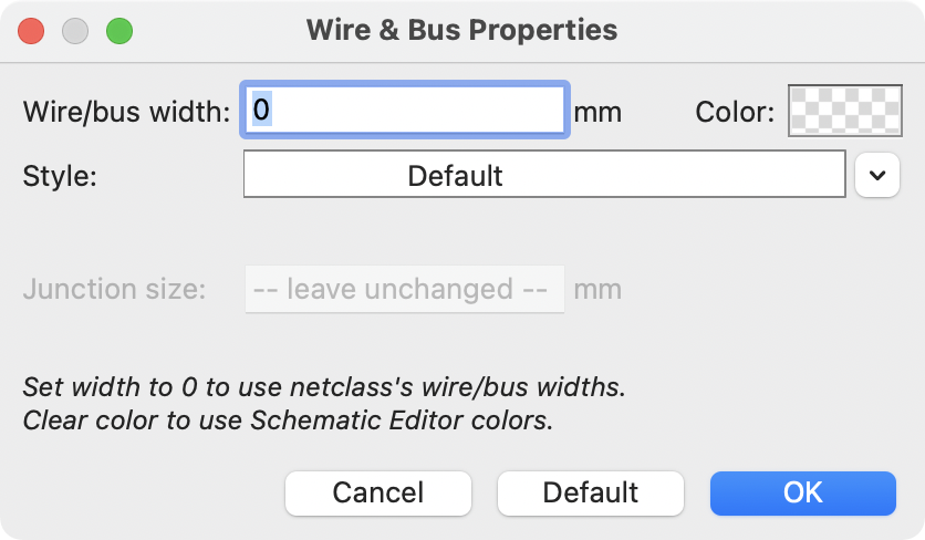
Normally the line style of a wire follows the
net’s netclass settings (nets are in the
Default netclass if no other netclass is specified). However, the line style
for the selected wire segments can be overridden in the wire’s properties dialog
(E when a wire segment is selected). The wire’s width, color, and line
style (solid, dashed, dotted, etc.) can be set. Setting the width to 0,
clearing the color, and using the Default line style uses the default width,
color, and style, respectively, from the netclass settings. If a wire junction
is included in the selection, the junction size can also be edited here.
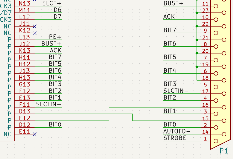
Wire Junctions
Wires that cross are not implicitly connected. It is necessary to
join them by explicitly adding a junction dot if a connection is desired
(![]() button in the right
toolbar). Junction dots will be automatically added to wires that start or end
on top of an existing wire.
button in the right
toolbar). Junction dots will be automatically added to wires that start or end
on top of an existing wire.
Junction dots are used in the schematic figure above on the wires connected to
P1 pins 18, 19, 20, 21, 22, and 23.
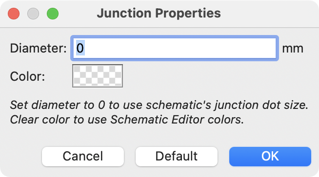
Junction size automatically follows the schematic’s Junction dot size
setting in Schematic Setup → General → Formatting. Color follows
the netclass setting. The automatic
size and color can be overridden in each junction dot’s properties; a size of
0 is equivalent to the schematic default size, and clearing the color uses the
netclass color.
Labels
Labels are used to assign net names to wires and pins. Wires with the same net name are considered to be connected, so labels can be used to make connections without drawing direct wire connections.
A net can only have one name. If two different labels are placed on the same net, an ERC violation will be generated. Only one of the net names will be used in the netlist. The final net name is determined according to the rules described below.
There are three types of labels, each with a different connection scope.
-
Local labels, also referred to simply as labels, only make connections within a sheet. Add a local label with the
 button in the right
toolbar.
button in the right
toolbar. -
Global labels make connections anywhere in a schematic, regardless of sheet. Add a global label with the
 button in the right
toolbar.
button in the right
toolbar. -
Hierarchical labels connect to hierarchical sheet pins and are used in hierarchical schematics for connecting child sheets to their parent sheet. Add a hierarchical label with the
 button in the right toolbar.
| Labels that have the same name will connect, regardless of the label type, if they are in the same sheet. |
Adding and editing labels
After using the appropriate button or hotkey to create a label, the Label Properties dialog appears.
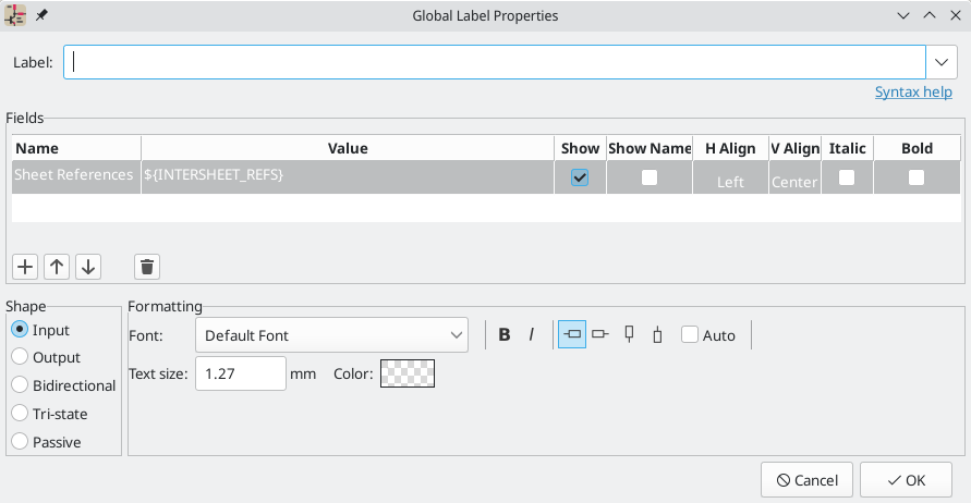
The Label field sets the label’s text, which determines the net that the label assigns to its attached wire. Label text supports markup for overbars, subscripts, etc., as well as variable substitution. Use the Syntax help link in the dialog for a summary.
There are several options to control the label’s appearance. You can change the font, size, and color of the text, and set bold and italic emphasis. You can also set the orientation of the text relative to the label’s connection point. Hierarchical and global labels have several additional options: the Auto option automatically sets the label orientation based on the connected schematic elements, and Shape option controls the shape of the label outline (Input, Output, Bidirectional, Tri-state, or Passive). The outline shape is purely visual and has no electrical consequence.
| The default text size can be set for a schematic in Schematic Setup, and the default font can be set in Preferences. |
| Global labels have additional settings to control margins around the label text in the Schematic Setup dialog. |
Labels can also have fields added to them. Two fields have special meaning (Net
Class and Sheet References, described below), but arbitrary fields can also
be added. Label fields behave like symbol fields:
you can show or hide their name and value and adjust the alignment, orientation,
position, size, font, color, and emphasis.
| Formatting options for label fields can be shown or hidden by right-clicking on the header row of the label field table and enabling or disabling the desired columns. Not all columns are shown by default. |
Like symbol fields, label fields can be edited individually by opening the properties of a specific label field from the schematic (double click the label field, or use E).
After accepting the label properties, the label is attached to the cursor for placement. The connection point for a label is the small square in the corner of the label. The square disappears when the label is connected to a wire or the end of a pin.

The connection point’s position relative to the label text can be changed by choosing a different label orientation in the label’s properties, or by mirroring/rotating the label.
The Label Properties dialog can be accessed at any time by selecting a label and using the E hotkey, double-clicking on the label, or with Properties… in the right-click context menu.
Assigning net classes with labels
In addition to assigning net names, labels can be used to assign net classes. A
label field named Net Class assigns the specified netclass to the net
associated with the label. To make it easier to assign net classes in this way,
Net Class is the default name for new label fields, and Net Class fields
present a dropdown list of all the net classes in the design. Net classes
must be created in the Schematic Setup or
Board Setup
windows before they can be assigned with a label field.
For more information about assigning netclasses, see the netclass documentation.
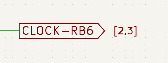
Inter-sheet references
Global labels can display inter-sheet references, which are a list of page numbers for other places in the schematic where the same global label appears. Clicking an inter-sheet reference travels to the listed page. If multiple references are listed, clicking the reference list brings up a menu to select the desired page.
Inter-sheet references are globally controlled in the Schematic Setup window’s Formatting page. References can be enabled or disabled, and the displayed format for the list can be adjusted, including with optional prefix or suffix characters.
The image below shows a global label with inter-sheet references to two other
schematic pages. A prefix and suffix of [ and ], respectively, were added in
Schematic Setup.
A Sheet References field with value ${INTERSHEET_REFS} is automatically
added to global labels, and is used to control the appearance of inter-sheet
references for that label. The ${INTERSHEET_REFS} text variable gets expanded
to the full list of inter-sheet references for the global label, as configured
in Schematic Setup. Visibility of inter-sheet references is globally controlled
in Schematic Setup rather than with the Sheet References field visibility
control. The Sheet References field has no meaning for other types of labels.
Buses
Buses are a way to group related signals in the schematic in order to
simplify complicated designs. Buses can be drawn like wires using the
bus tool ![]() , and are named using
labels the same way signal wires are.
, and are named using
labels the same way signal wires are.
In the following schematic, many pins are connected to buses, which are the thick blue lines in the center.
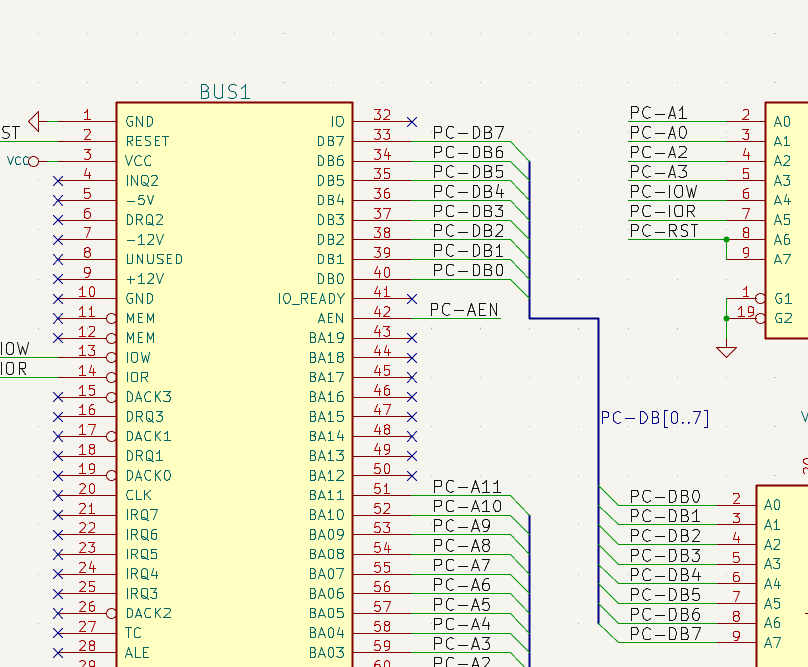
Bus members
There are two types of bus in KiCad 6.0 and later: vector buses and group buses.
A vector bus is a collection of signals that start with a common prefix
and end with a number. Vector buses are named <PREFIX>[M..N] where
PREFIX is any valid signal name, M is the first suffix number, and N
is the last suffix number. For example, the bus DATA[0..7] contains the
signals DATA0, DATA1, and so on up to DATA7. It doesn’t matter which
order M and N are specified in, but both must be non-negative.
A group bus is a collection of one or more signals and/or vector buses. Group buses can be used to bundle together related signals even when they have different names. Group buses use a special label syntax:
<OPTIONAL_NAME>{SIGNAL1 SIGNAL2 SIGNAL3}
The members of the group are listed inside curly braces ({}) separated
by space characters. An optional name for the group goes before the opening
curly brace. If the group bus is unnamed, the resulting nets on the PCB
will just be the signal names inside the group. If the group bus has a
name, the resulting nets will have the name as a prefix, with a period (.)
separating the prefix from the signal name.
For example, the bus {SCL SDA} has two signal members, and in the netlist
these signals will be SCL and SDA. The bus USB1{DP DM} will generate
nets called USB1.DP and USB1.DM. For designs with larger buses that are
repeated across several similar circuits, using this technique can save time.
Group buses can also contain vector buses. For example, the bus
MEMORY{A[7..0] D[7..0] OE WE} contains both vector buses and plain signals,
and will result in nets such as MEMORY.A7 and MEMORY.OE on the PCB.
Bus wires can be drawn and connected in the same manner as signal wires, including using junctions to create connections between crossing wires. Like signals, buses cannot have more than one name — if two conflicting labels are attached to the same bus, an ERC violation will be generated.
Connections between bus members
Pins connected between the same members of a bus must be connected by labels. It is not possible to connect a pin directly to a bus; this type of connection will be ignored by KiCad.
In the example above, connections are made by the labels placed on wires connected to the pins. Bus entries (wire segments at 45 degrees) to buses are graphical only, and are not necessary to form logical connections.
In fact, using the repetition command (Insert), connections can be very quickly made in the following way, if component pins are aligned in increasing order (a common case in practice on components such as memories, microprocessors…):
-
Place the first label (for example
PCA0) -
Use the repetition command as much as needed to place members. KiCad will automatically create the next labels (
PCA1,PCA2…) vertically aligned, theoretically on the position of the other pins. -
Draw the wire under the first label. Then use the repetition command to place the other wires under the labels.
-
If needed, place the bus entries by the same way (Place the first entry, then use the repetition command).
|
In the Schematic Editor → Editing Options section of the Preferences menu, you can set the repetition parameters:
|
Bus unfolding
The unfold tool allows you to quickly break out signals from a bus. To unfold a signal, right-click on a bus object (a bus wire, etc) and choose Unfold from Bus. Alternatively, use the Unfold Bus hotkey (default: C) when the cursor is over a bus object. The menu allows you to select which bus member to unfold.
After selecting the bus member, the next click will place the bus member label at the desired location. The tool automatically generates a bus entry and wire leading up to the label location. After placing the label, you can continue placing additional wire segments (for example, to connect to a component pin) and complete the wire in any of the normal ways.
Bus aliases
Bus aliases are shortcuts that allow you to work with large group buses more efficiently. They allow you to define a group bus and give it a short name that can then be used instead of the full group name across the schematic.
To create bus aliases, open the Bus Alias Definitions pane in Schematic Setup.
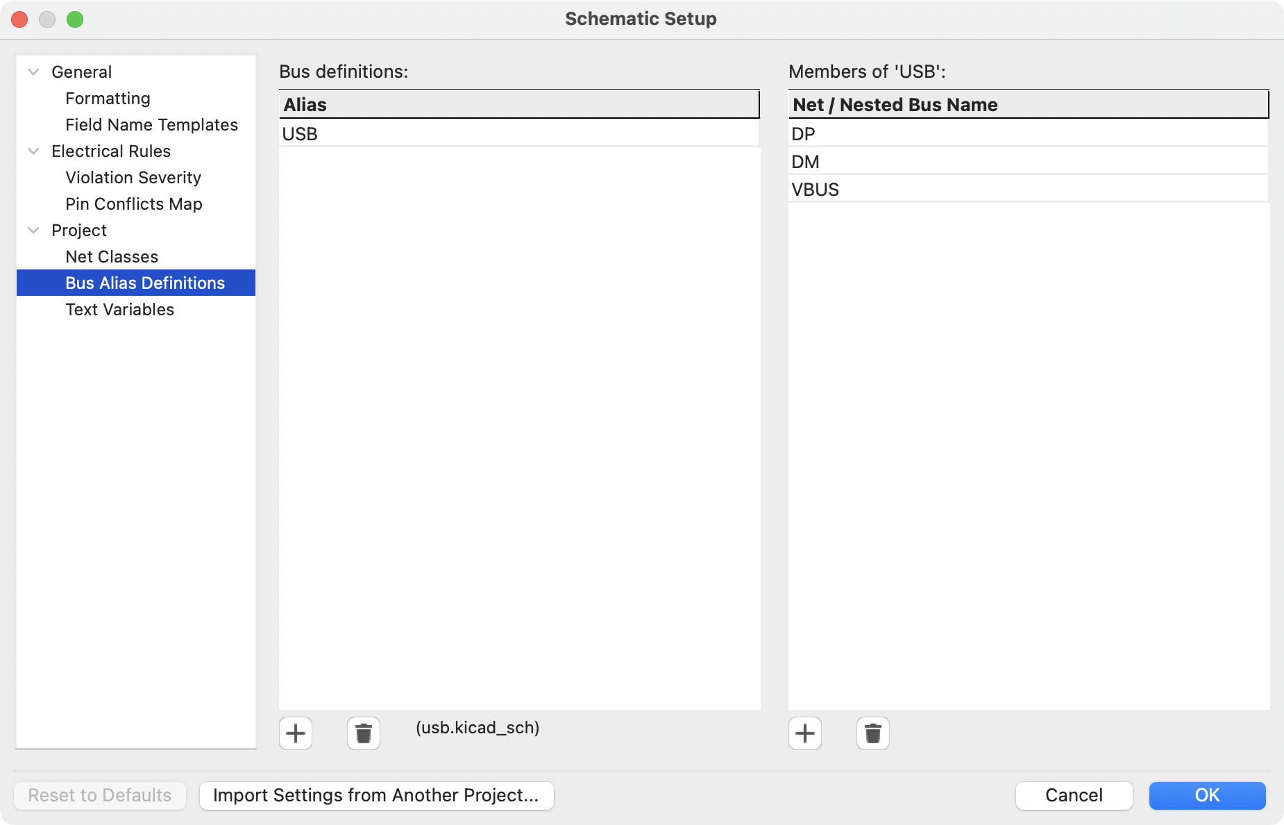
An alias may be named any valid signal name. Using the dialog, you can add
signals or vector buses to the alias. As a shortcut, you can type or paste
in a list of signals and/or buses separated by spaces, and they will all be
added to the alias definition. In this example, we define an alias called
USB with members DP, DM, and VBUS.
After defining an alias, it can be used in a group bus label by putting the
alias name inside the curly braces of the group bus: {USB}. This has the
same effect as labeling the bus {DP DM VBUS}. You can also add a prefix
name to the group, such as USB1{USB}, which results in nets such as
USB1.DP as described above. For complicated buses, using aliases can
make the labels on your schematic much shorter. Keep in mind that the aliases
are just a shortcut, and the name of the alias is not included in the netlist.
Bus aliases are saved in the schematic file that is opened when the alias is created. The Bus Alias Definitions window shows the schematic file associated with the selected alias at the bottom of the alias list. Any aliases created in a given schematic sheet are available to use in any other schematic sheet that is in the same hierarchical design. If multiple sheets in a hierarchical design contain identically-named bus aliases, the aliases must all have the same members. ERC will report a violation if multiple bus aliases with the same name do not have consistent members.
Buses with more than one label
KiCad 5.0 and earlier allowed the connection of bus wires with different labels together, and would join the members of these buses during netlisting. This behavior has been removed in KiCad 6.0 because it is incompatible with group buses, and also leads to confusing netlists because the name that a given signal will receive is not easily predicted.
If you open a design that made use of this feature in a modern version of KiCad, you will see the Migrate Buses dialog which guides you through updating the schematic so that only one label exists on any given set of bus wires.
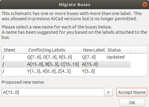
For each set of bus wires that has more than one label, you must choose the label to keep. The drop-down name box lets you choose between the labels that exist in the design, or you can choose a different name by manually entering it into the new name field.
Hidden Power Pins
When the power pins of a symbol are visible, they must be connected, as with any other signal. However, symbols such as gates and flip-flops are sometimes drawn with hidden power input pins which are connected implicitly.
KiCad automatically connects invisible pins with type "power input" to a global
net with the same name as the pin. For example, if a symbol has a hidden power
input pin named VCC, this pin will be globally connected to the VCC net on
all sheets.
|
Hidden pins can be shown in the schematic by checking the Show hidden
pins option in the Schematic Editor → Display Options section
of the preferences, or by selecting View → Show hidden pins.
There is also a toggle icon |
It may be necessary to join power nets of different names (for example, GND in
TTL components and VSS in MOS components). To accomplish this, add a
power symbol for each net and connect them with a wire.
If hidden power pins are used, it is not recommended to use local labels for power connection, as they will not connect to hidden power pins on other sheets.
| Care must be taken with hidden power input pins because they can create unintentional connections. By nature, hidden pins are invisible and do not display their pin name. This makes it easy to accidentally connect two power pins to the same net. For this reason, using invisible power pins in symbols is not recommended outside of power symbols, and is only supported for compatibility with legacy designs and symbols. |
Power Symbols
Power symbols are symbols that are conventionally used to represent a connection
to a power net, such as VCC or GND. In addition to being a visual indicator
that the attached net is a power rail, power symbols make global connections:
two power symbols with the same pin name connect to each other anywhere in the
schematic, regardless of sheet.
Power symbols are virtual: they do not represent a physical component on the PCB.
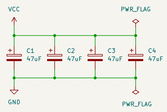
In the figure below, power symbols are used to connect the positive and negative
terminals of the capacitors to the VCC and GND nets, respectively.
In the KiCad standard library, power symbols are found in the power library, but
power symbols can be created in any library.
To create a custom power symbol, make a new symbol with a power input pin that is set to be invisible. Name the pin according to the desired power net. In addition, set the "Define as power symbol" symbol property. As described in the hidden power pins section, invisible power input pins make global connections based on the hidden power pin’s name. The process of creating a power symbol is described in more detail in the Symbol Editor section.
| The connected net name is determined by the power symbol’s pin name, not the name or value of the symbol. This means that power symbol net names can only be changed in the symbol editor, not in the schematic. |
Net name assignment rules
Every net in the schematic is assigned a name, whether that name is specified by the user or automatically generated by KiCad.
When multiple labels are attached to the same net, the final net name is determined in the following order, from highest priority to lowest:
-
Global labels
-
Local labels
-
Hierarchical labels
-
Hierarchical sheet pins
If there are multiple labels of one type attached to a net, the names are sorted alphabetically and the first is used.
If a net travels through multiple sheets of a hierarchy, it will take its name from the highest level of the hierarchy where it has a hierarchical label or local label. As usual, local labels take priority over hierarchical labels.
If none of the label types above are attached to a net, the net’s name is automatically generated based on the connected symbol pins.
PWR_FLAG
Two PWR_FLAG symbols are visible in the screenshot above. They indicate to ERC
that the two power nets VCC and GND are actually connected to a power
source, as there is no explicit power source such as a voltage regulator output
attached to either net.
Without these two flags, the ERC tool would diagnose: Error: Input Power pin not driven by any Output Power pins.
The PWR_FLAG symbol is found in the power symbol library. The same effect
can be achieved by connecting any power output pin to the net.
No-connection flag
No-connection flags (![]() ) are
used to indicate that a pin is intentionally unconnected. These flags prevent
"unconnected pin" ERC warnings for pins that are intentionally
unconnected.
) are
used to indicate that a pin is intentionally unconnected. These flags prevent
"unconnected pin" ERC warnings for pins that are intentionally
unconnected.
Note that no-connection flags are distinct from the "unconnected" symbol pin type, although they both prevent "unconnected pin" ERC warnings on the pin in question.
Netclasses
Netclasses are groups of nets that can be assigned design rules (for the PCB) and graphical properties (for the schematic). In KiCad, each net is part of exactly one net class. If you do not add a net to a specific class, it will be part of the Default class, which always exists.
Net classes may be created and edited in either the Schematic or Board Setup dialogs. Nets can be added to netclasses in either the schematic or board using pattern-based assignments described below. Nets can also be assigned to netclasses in the schematic using graphical assignments with net class directives or net labels.
Selecting a wire or label displays the net’s netclass in the message panel at the bottom of the window.
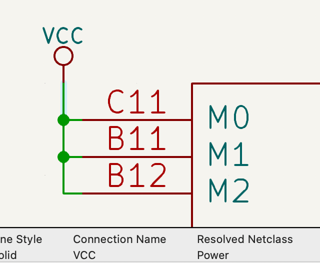
Managing netclasses in Schematic Setup
Netclasses are managed in the Net Classes panel of the Schematic Setup dialog.
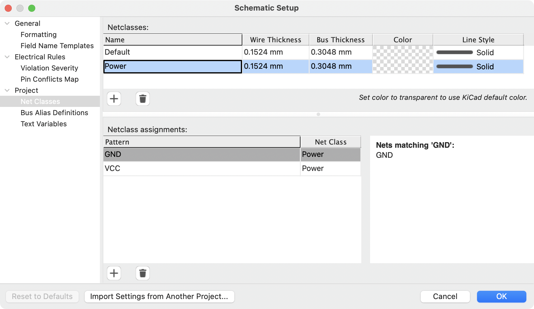
The top pane lists the netclasses that exist in the design. The Default
netclass always exists, and you can add additional netclasses with the
![]() button or remove the
selected netclass with the
button or remove the
selected netclass with the
![]() button.
button.
Each netclass can have unique graphic properties that determine how wires of that netclass are displayed in the schematic. Wire and bus thicknesses, color, and line style (solid, dashed, dotted, etc.) can all be adjusted. Setting the color to transparent will use the theme’s default wire/bus color for the netclass, which is configurable in Preferences.
You can also set board design rules for each netclass, although the DRC fields are hidden by default. Right click the header row to show or hide additional columns. For more information about setting netclass design rules, see the PCB editor documentation.
The bottom pane lists pattern-based netclass assignments. Each row has a net
name pattern and a netclass; nets with names that match the pattern are assigned
to the specified netclass. If a net matches multiple patterns, the first match
is used. Pattern-based netclass assignments are dynamic: when a new net is added
that matches an existing pattern, it will be assigned to the associated netclass
automatically. Net patterns can use both wildcards (* to match any number of
any characters, including none, and ? to match any character) and
regular expressions. The
nets that match the selected pattern are displayed to the right of the pattern
list.
For example, the net* pattern matches nets named net, net1, network, and
any other net name beginning with net. Because * has a slightly different
meaning in a regular expression (* matches zero or more of the preceding
character), the net* pattern would also match a net named ne.
Remember that net names must include the full sheet path. For example, a
locally labeled net in the root sheet has a name prefixed with /.
|
Use the ![]() button to add
a net class assignment pattern or the
button to add
a net class assignment pattern or the
![]() button to remove a
pattern.
button to remove a
pattern.
A netclass pattern containing only the * wildcard will match all
explicitly named nets, but will not match unlabeled nets. To match
unlabeled nets, you can include more of the net name before the wildcard
character. All unlabeled nets have names that begin with Net-, so the
pattern Net-* will match all unlabeled nets. You can also assign a
netclass to an unlabeled net using a
net class directive.
|
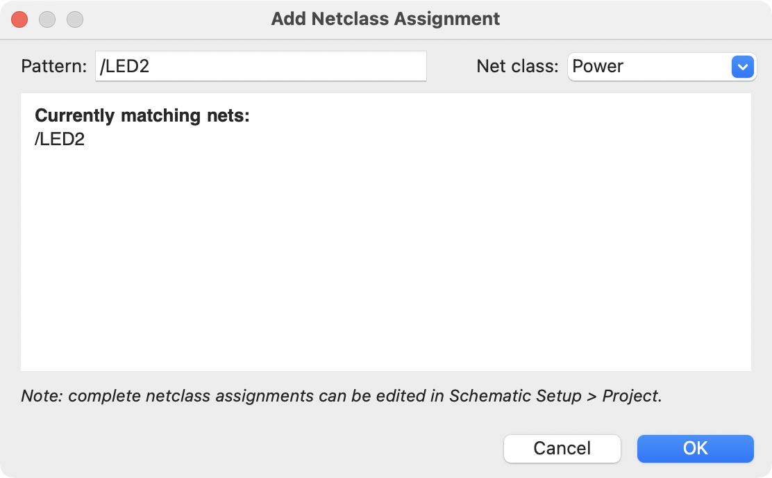
Instead of adding netclass patterns in the Schematic Setup dialog, you can directly create netclass patterns from the schematic canvas. Right click a net and select Assign Netclass… to bring up the Add Netclass Assignment dialog. The netclass pattern is pre-filled with the name of the selected net, but the pattern can be changed if desired. All nets matching the pattern are displayed in the dialog.
Graphically assigning netclasses in the schematic
As an alternative to pattern-based netclass assignment, netclasses can be graphically assigned to nets in the schematic using either net class directives or labels. Netclasses must be created in Schematic Setup before they can be assigned graphically.
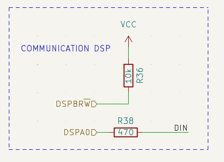
In the image below, a net class directive is used to assign signals to the 50R
netclass.
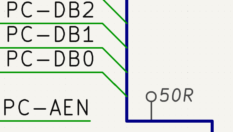
Net class directives are added with the
![]() button in the
right toolbar. They behave like labels, except that they cannot be
used to name a net. The attached net is assigned a netclass according to the
value of the directive’s
button in the
right toolbar. They behave like labels, except that they cannot be
used to name a net. The attached net is assigned a netclass according to the
value of the directive’s Net Class field. The Net Class field presents a
dropdown list of all the net classes in the design.
If a directive is attached to a bus, all members of the bus are assigned to the specified net class.
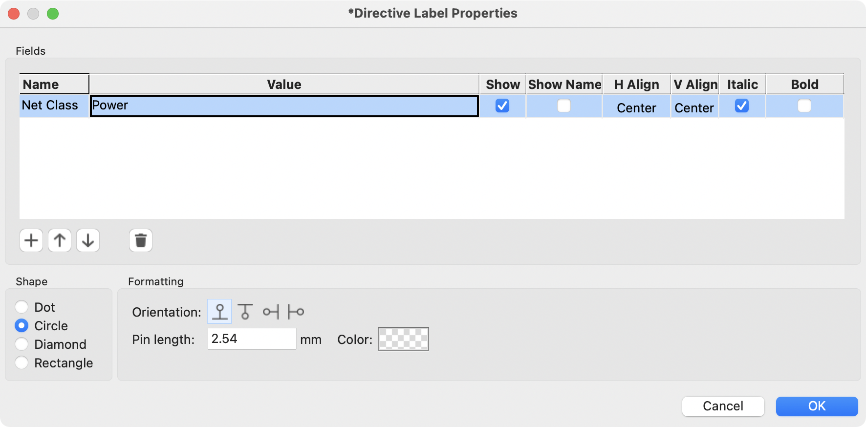
In addition to the associated netclass, you can edit the directive’s shape (dot, circle, diamond, or rectangle), orientation, pin length, and color in the directive’s properties.
Net labels can also be used to assign netclasses to nets by
adding a Net Class field to the label.
If more than one different netclass is graphically assigned to a single net, ERC will report an issue. Graphical netclass assignments override pattern-based assignments: if a net matches a netclass pattern assignment and also has a netclass assigned graphically, the graphically assigned netclass will be used.
Graphical items
Text, graphic shapes, and images can be added to schematics for documentation purposes. These items do not have any electrical effect on the schematic.
The image below shows graphic lines and text ("COMMUNICATION DSP") in addition to symbols and several types of labels.
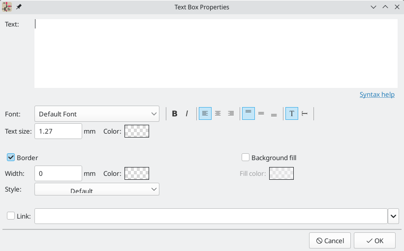
Text and Text Boxes
Two kinds of text can be added to schematics, which are referred to as text
(![]() ) and text boxes
(
) and text boxes
(![]() ). Both are added using
their respective buttons in the right toolbar.
). Both are added using
their respective buttons in the right toolbar.
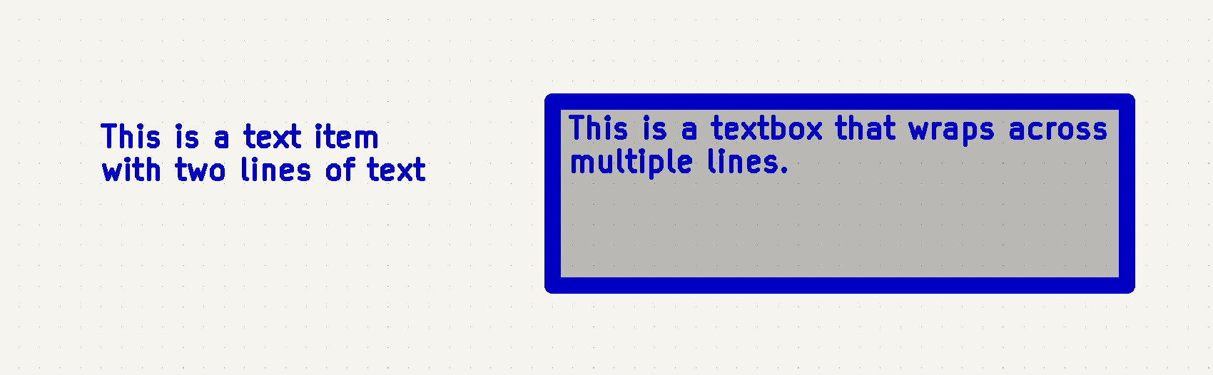
Both kinds of text item support multiline text and basic formatting features, but text boxes wrap text to fit in the outline and have additional formatting options. All text has adjustable fonts, color, size, bold and italic emphasis, left and right alignment, and vertical and horizontal orientation. Text boxes additionally support horizontal centering, vertical alignment options, and colored borders and fill.
| The default text size can be set for a schematic in Schematic Setup, and the default font can be set in Preferences. |
Links
Text and text boxes can be made into a link by entering a target in the Link
box in the text properties. The link target can be a local file (using the
file:// protocol prefix followed by the file’s path), to a website (using
http:// or https:// followed by the rest of the URL), or to another page in
the same schematic (using # followed by the page number). These can also be
autofilled using the dropdown menu in the link target box.
Fonts
Text and text boxes support custom fonts, which are selectable with the Font dropdown in the properties dialog for the text. In addition to the KiCad font, you can use any TTF font installed on your computer.
| User fonts are not embedded in the project. If the project is opened on another computer that does not have the selected font installed, a different font will be substituted. For maximum compatibility, use the KiCad font. |
Text Markup
Text supports markup for superscripts, subscripts, overbars, evaluating project variables, and accessing symbol field values.
| Feature | Markup Syntax | Result |
|---|---|---|
Superscript |
|
textsuperscript |
Subscript |
|
textsubscript |
Overbar |
|
text |
|
variable_value |
|
|
field_value of symbol refdes |
| Variables must be defined in Schematic Setup before they can be used. There are also a number of built-in system text variables. |
Graphic Shapes
Graphic rectangles (![]() ), circles (
), circles (![]() ), arcs
(
), arcs
(![]() ), and lines
(
), and lines
(![]() ) can all be added
using their respective buttons in the right toolbar.
) can all be added
using their respective buttons in the right toolbar.

Line width, color, and style (solid, dashed, or dotted) can be configured in the properties dialog for each shape (E). Rectangles, circles, and arcs can also have a fill color set and have their outlines removed.
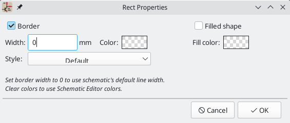
Setting a shape’s line width to 0 uses the schematic default line width, which is configurable in Schematic Setup. Spacing for line dashes is also configurable there. Removing a line or fill color uses the color theme’s graphics color, which is configurable in Preferences.
Like wires, graphic lines obey the line drawing
mode setting (90 degree, 45 degree, or free angle), which you can set using the
toggle buttons on the left toolbar
(![]() ,
,
![]() , and
, and
![]() , respectively).
Shift+Space cycles through the modes.
, respectively).
Shift+Space cycles through the modes.
As with PCB tracks, the / hotkey switches line posture.
Bitmap Images
Bitmap images can be added to the schematic with the
![]() button. Images in the
schematic can be moved and scaled. The properties dialog allows setting a
location and scale as well as converting the image to greyscale.
button. Images in the
schematic can be moved and scaled. The properties dialog allows setting a
location and scale as well as converting the image to greyscale.
Bulk editing text and graphics
Properties of text and graphics can be edited in bulk using the Edit Text and Graphic Properties dialog (Tools → Edit Text and Graphic Properties…). The tool can also modify visual properties of wires and buses.
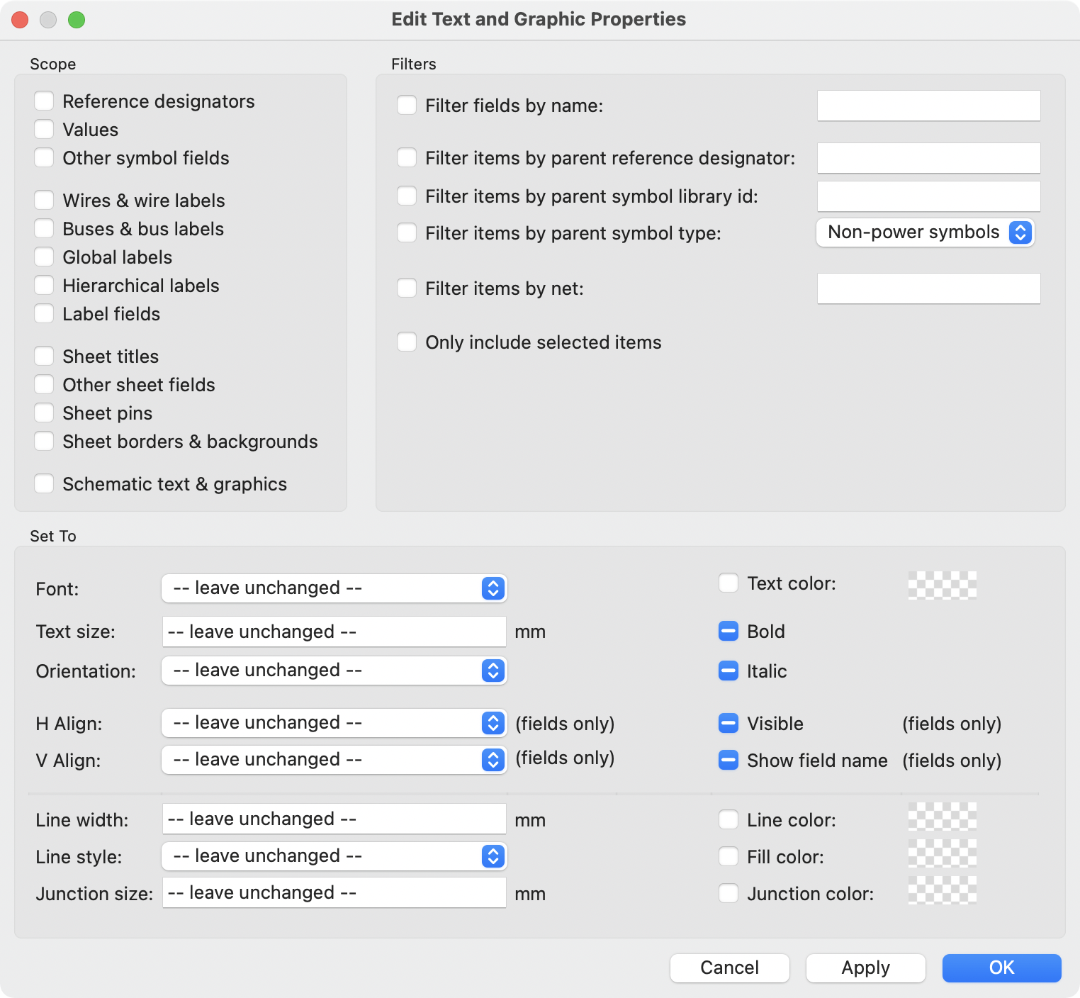
Scope and Filters
Scope settings restrict the tool to editing only certain types of objects. If no scopes are selected, nothing will be edited.
Filters restrict the tool to editing particular objects in the selected scope.
Objects will only be modified if they match all enabled and relevant filters
(some filters do not apply to certain types of objects. For example, symbol
field filters do not apply to wires and are ignored for the purpose of changing
wire properties). If no filters are enabled, all objects in the selected scope
will be modified. For filters with a text box, wildcards are supported: *
matches any number of any characters, including none, and ? matches any single
character.
Filter fields by name filters to the specified symbol, label, or sheet field.
Filter items by parent reference designator filters to fields in the symbol with the specified reference designator. Filter items by parent symbol library id filters to fields in symbols with the specified library identifier. Filter items by parent symbol type filters to fields in symbols of the selected type (power or non-power).
Filter items by net filters to wires and labels on the specified net.
Only include selected items filters to the current selection.
Editable Properties
Properties for filtered objects can be set to new values in the bottom part of the dialog.
Drop-down lists and text boxes can be set to -- leave unchanged -- to preserve
existing values. Checkboxes can be checked or unchecked to enable or disable a
change, but can also be toggled to a third "leave unchanged" state. Color
properties must be checked to change the value; a checkerboard swatch indicates
that the color will be inherited from the default value from the the schematic
settings or netclass properties.
Text properties that can be modified are font, text size, text orientation (right/up/leftdown), horizontal and vertical alignment, text color, emphasis (bold and italic), and visibility of fields and field names.
Graphic and wire properties that can be modified are line width, line style (solid, dashed, and dotted lines), line color, fill color for shapes, and junction size and junction color for wire junctions.
Sheet title block
The title block is edited with the Page Settings tool
(![]() ).
).
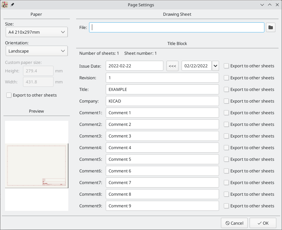
Each field in the title block can be edited, as well as the paper size and orientation. If the Export to other sheets option is checked for a field, that field will be updated in the title block of all sheets, rather than only the current sheet.
You can set the date to today’s or any other date by pressing the left arrow button next to Issue Date. Note that the date in the schematic will not be automatically updated.
A drawing sheet template file can also be selected.
The sheet number (Sheet X/Y) is automatically updated, but sheet page numbers can also be manually set using Edit → Edit Sheet Page Number….
Schematic Setup
The Schematic Setup window is used to set schematic options that are specific to the currently active schematic. For example, the Schematic Setup window contains formatting options, electrical rule configuration, netclass setup, and schematic text variable setup.
You can import schematic settings from an existing project using the Import Settings from Another Project… button. This allows you to choose a project to use as a template and select which settings to import (formatting preferences, field name templates, pin conflict map, violation severities, and net classes).
Schematic formatting
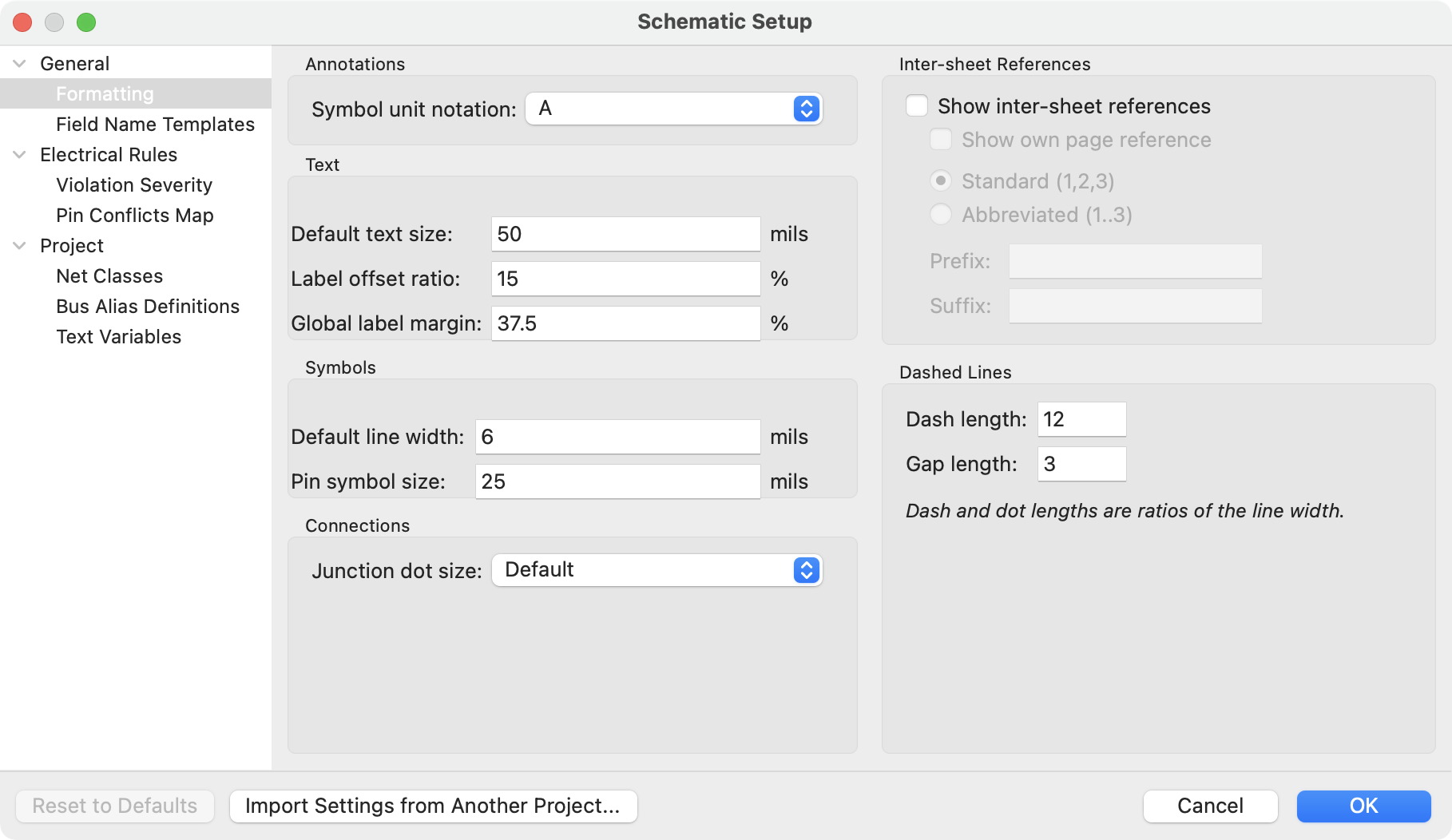
The formatting panel contains settings for the appearance of symbols, text, labels, graphics, and wires.
Symbol unit notation sets how each unit of a multi-unit symbol is referred to
in its reference designator. By default, a different letter for each unit is
appended to the reference designator with no separator, for example U1B for
the second unit of symbol U1, but this can be changed. Numbers can be used
instead of letters, and various separators can be used between the symbol
designator and the unit identifier (., -, _, or none).
Default text size sets the default text height used by the text, text box, and
label tools. Label offset ratio controls the vertical spacing between a local
label’s text and the attached wire, relative to the label’s text size. This also
affects the spacing between symbol pins and their pin number.
Global label margin defines the size of the box around a global label,
relative to the global label’s text size. Increasing the margin may be useful
to avoid overlapping text with overbars (~{}) or letters with descenders, but
this may cause closely packed global labels to overlap with each other.
Default line width sets the default line width for symbol graphics, if the symbol does not override the default line width. Pin symbol size scales symbol pin graphic style annotations, such as the bubble on an inverted pin.
Junction dot size sets the schematic’s default wire junction dot size. The default size can be overridden by editing an individual junction dot’s properties.
Show inter-sheet references enables or disables the display of
inter-sheet references, which are a list of page
numbers next to a global labels that link to other places in the schematic where
the same global label appears. Show own page reference controls whether the
current page is included in the list of page numbers. Standard and
abbreviated determine whether to display the complete list of page numbers or
only the first and last page numbers. The prefix and suffix fields add
optional characters before and after the list of page numbers. In the image
of an inter-sheet reference below, a prefix and suffix of [ and ],
respectively, have been added.
Dashed line appearance is controlled in the Formatting section. Dash length
controls the length of dashes, while Gap length controls the spacing between
dashes and dots. The dash and gap lengths are relative to the line width: a gap
length of 2 means twice the width of the line.
Field name templates
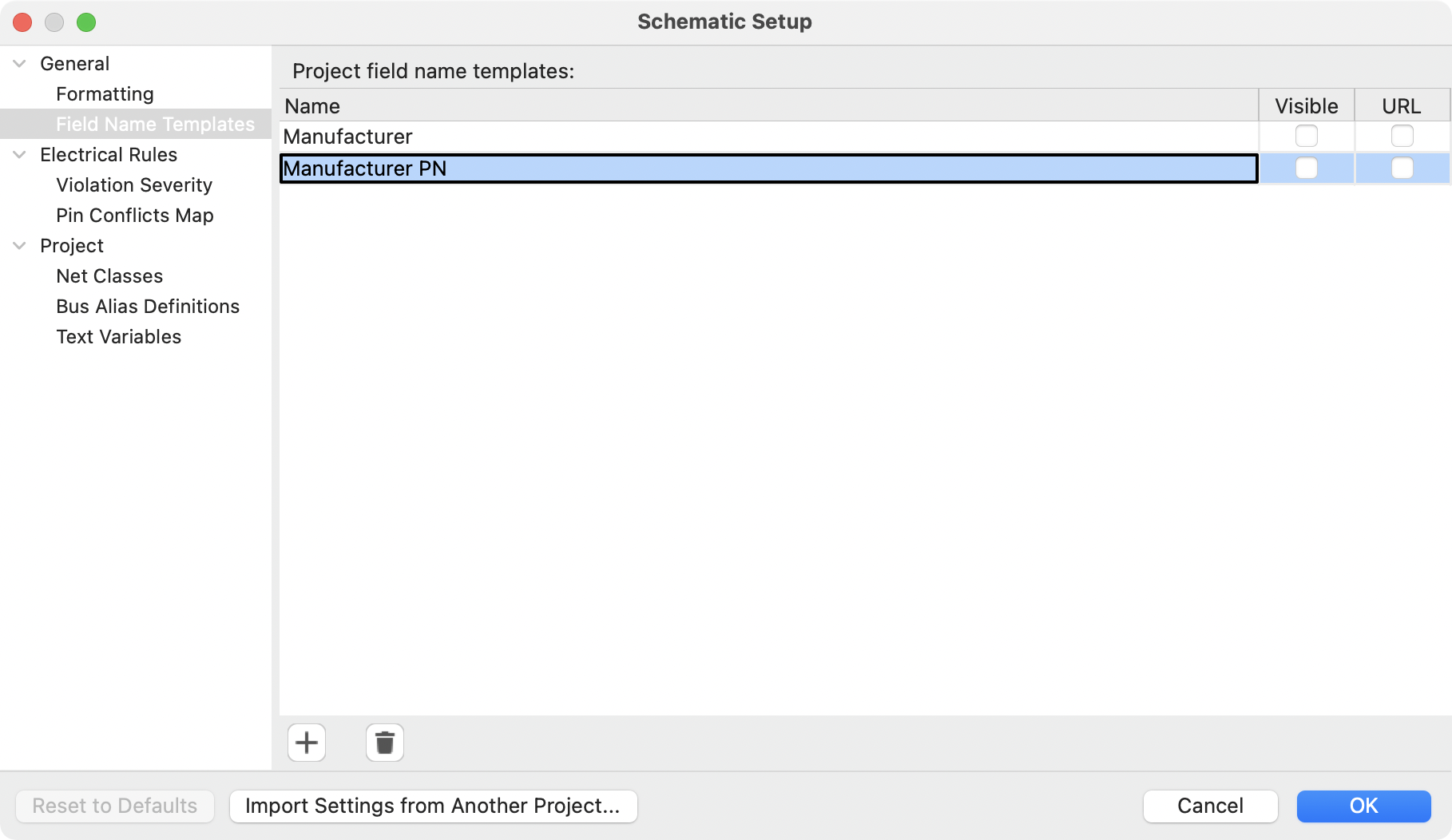
Field name templates are empty symbol fields that are automatically added to all symbols in the schematic. These can be useful when every symbol in the schematic needs additional fields beyond the fields that are defined in the library symbols, for example a field for the manufacturer’s part number.
Template fields can be set as visible or invisible, and can also be set as URL fields.
Field name templates that are defined in schematic setup apply only to the current project. Field name templates can also be defined in Preferences, which apply to all projects edited on your computer.
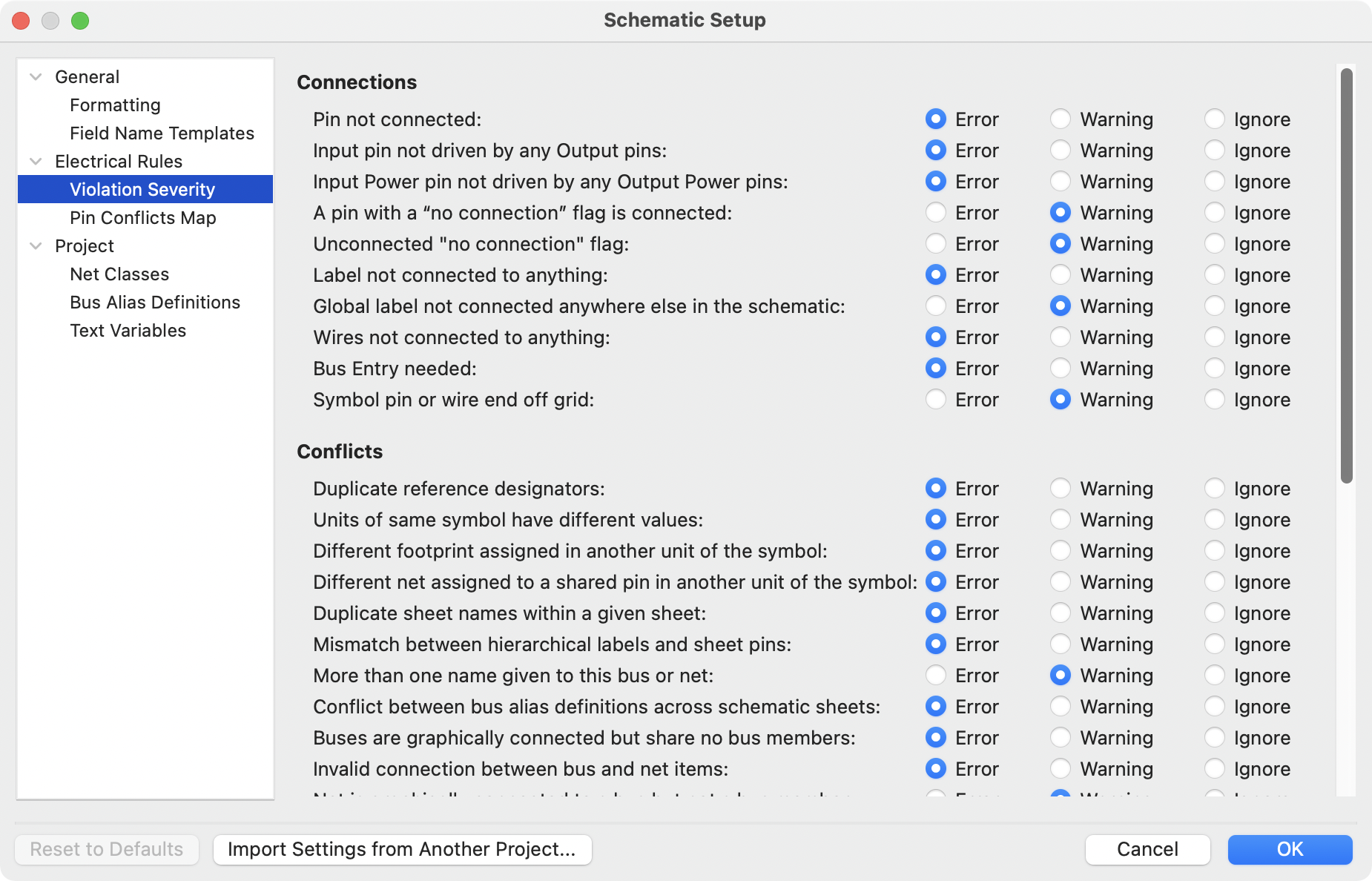
ERC violation severity and pin conflicts map
The Violation Severity panel lets you configure what types of ERC messages should be reported as Errors, Warnings, or ignored.
The Pin Conflicts Map allows you to configure connectivity rules to define electrical conditions for errors and warnings based on what types of pins are connected to each other. For example, by default an error is produced when an output pin is connected to another output pin.
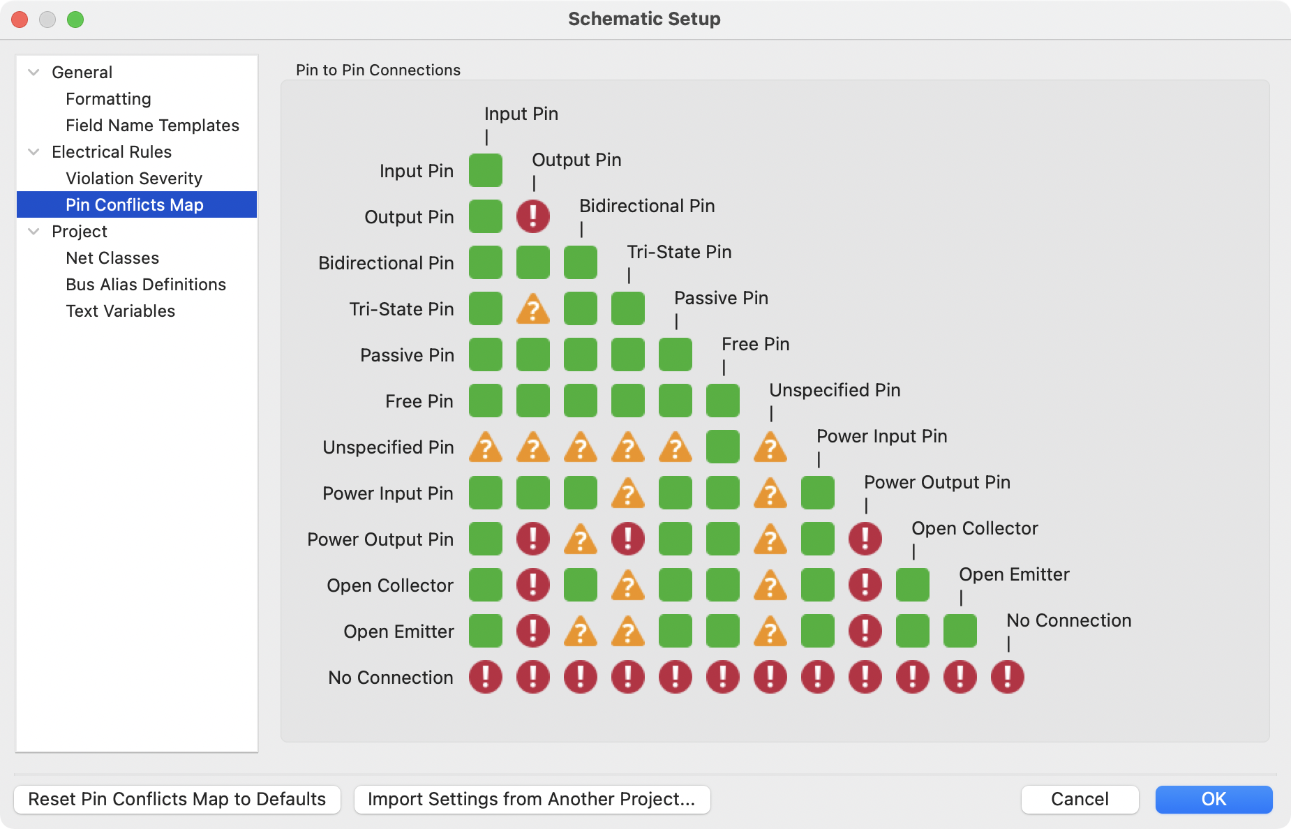
These panels are explained in more detail in the ERC section.
Net classes
The Net Classes panel allows you to manage netclasses for the project and assign nets to netclasses with patterns. Managing netclasses in this panel is equivalent to managing them in the Board Setup dialog. Nets can also be assigned to netclasses in the schematic using graphical assignments with net class directives or net labels.
Pattern-based netclass assigment is explained in more detail in the net classes section.
Bus alias definitions
The Bus Alias Definitions panel allows you to create bus aliases, which are names for groups of signals in a bus. For more information about bus aliases, see the bus alias documentation.
Text variables
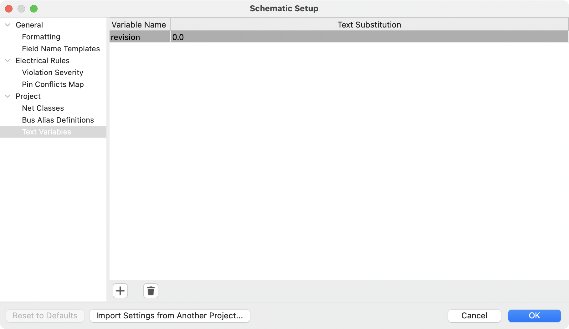
Text replacement variables can be created in the Text Variables section. These
variables allow you to substitute the variable name for any text string. This
substitution happens anywhere the variable name is used inside the variable
replacement syntax of ${VARIABLENAME}.
For example, you could create a variable named VERSION and set the text
substitution to 1.0. Now, in any text object on the PCB, you can enter
${VERSION} and KiCad will substitute 1.0. If you change the substitution to
2.0, every text object that includes ${VERSION} will be updated
automatically. You can also mix regular text and variables. For example, you
can create a text object with the text Version: ${VERSION} which will be
substituted as Version: 1.0.
Text variables can also be created in Board Setup. Text variables are project-wide; variables created in the schematic editor are also available in the board editor, and vice versa.
There are also a number of built-in system text variables.
Opening legacy schematics
Modern versions of KiCad can always open projects created in older versions of KiCad. However, schematics created in some older versions of KiCad have special considerations that must be observed when opening them in order to prevent any data loss.
Opening KiCad 5.0 and 5.1 schematics
Modern versions of KiCad can open schematics created in versions prior to KiCad
6.0, but the cache library file (<projectname>-cache.lib) must be present to
load the schematic correctly.
Since version 6.0, KiCad stores all symbols used in a project in the schematic.
This means that you can open a schematic made in KiCad 6.0 or later on any
computer, even if the libraries used in the project are not installed or have
changed. Modern KiCad schematic files use the .kicad_sch extension.
Prior to version 6.0, KiCad did not store symbols in the schematic. Instead,
KiCad stored references to the symbols and their libraries. It also stored a
copy of every symbol used by the project in a separate cache library file
(<projectname>-cache.lib). As long as the cache library was included with the
project, the project could be distributed without the system library files,
because KiCad could load any needed symbols from the cache library as a fallback
if the libraries referenced in the schematic were missing. Legacy KiCad
schematic files use the .sch extension.
When you open a legacy schematic, KiCad will look in the cache library to find
all of the symbols used in the schematic in the cache library. When you save the
legacy schematic, KiCad will save it as a new file in the modern schematic
format (.kicad_sch), with the necessary symbols embedded in the schematic
itself. The original legacy schematic and the cache library will remain,
unmodified, but they are no longer necessary once the schematic has been saved
in the modern format.
| Projects created in KiCad prior to version 6.0 must have a cache library. If the cache library is missing, the schematic will lose symbol information if the system symbol libraries are modified, reorganized, moved, or deleted. The libraries included with legacy versions of KiCad are substantially different than the modern KiCad libraries, so in practice KiCad will almost always fail to open legacy projects unless the cache library is present. |
When you open a legacy schematic, KiCad may display the Project Rescue Helper dialog. This means that one or more symbols in the cache library do not match the corresponding symbol in the external library. The dialog helps you "rescue" symbols from the cache library into your schematic, if desired. You can also open the rescue dialog at any time using Tools → Rescue Symbols…. The cache library file must be present in order to use the rescue tool.
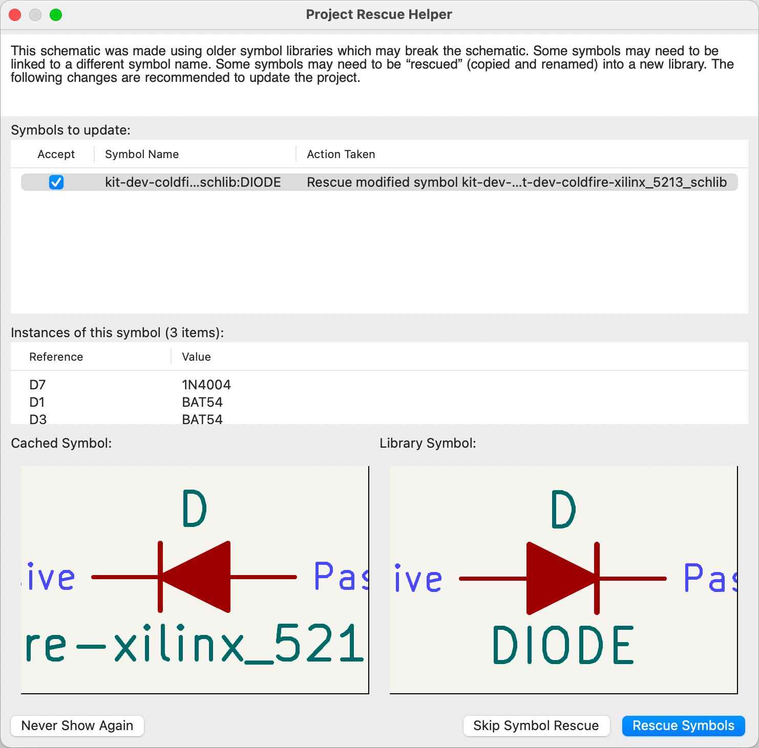
The rescue dialog lists all symbols that don’t match between the cache library and the external symbol library. The discrepancy can be because:
-
the cached symbol or the library symbol has been modified, so the two symbols no longer match, or
-
the cached symbol does not have a corresponding symbol in the symbol library, because the symbol or library was moved, renamed, deleted, or is not present on the current computer.
For each symbol in the list, selecting the symbol displays the reference designator and value for each instance of the symbol, and shows a visual preview of the symbol. If a corresponding symbol exists in the system symbol library, the dialog shows both copies of the symbol for comparison. If the symbol only exists in the cache library, the dialog only shows the cached symbol.
In this example, the project originally used a diode with the cathode facing left, but the library now contains one with the cathode facing right. This change would break the design, so it would be important to use the cached symbol as the original designer intended.
Pressing Rescue Symbols here will cause the selected symbols from the cache
library to be saved into a special rescue library
(<projectname>-rescue.kicad_sym). The corresponding symbols in the schematic
will be updated to use the newly rescued symbols. Any unselected symbols will
not be rescued, but their symbol linkage can be updated in the schematic later.
Alternatively, pressing Skip Symbol Rescue will exit the dialog without rescuing any symbols. KiCad will use the versions of the symbols found in the external libraries. You can run the rescue function again with Tools → Rescue Symbols…, or manually edit symbol linkage in the symbol’s properties.
If you would prefer not to see this dialog, you can press Never Show Again. This has the same effect as pressing Skip Symbol Rescue for the current schematic and all future schematics.
If a symbol in a legacy schematic cannot be found in either the cache library or the external library, KiCad cannot rescue that symbol. A placeholder symbol is inserted into the schematic in its place, as shown below.
You can attempt to remap these orphaned symbols using the Change Symbols or Edit Symbol Library Links dialogs, but either option may require manual corrections to the schematic. These tools are explained in more detail in the Updating and exchanging symbols section.
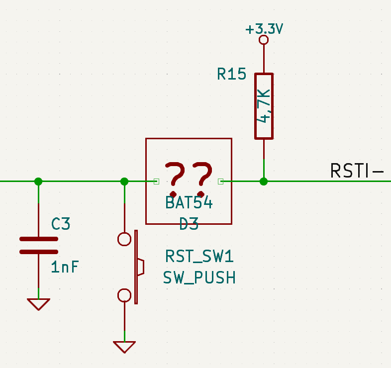
Opening pre-5.0 schematics
Modern versions of KiCad can open schematics created in versions prior to KiCad 5.0, but you will need to go through a symbol remapping process to open the schematic without losing symbol information.
Since version 5.0, KiCad schematics refer to specific symbols using both the symbol and library name. Even if multiple libraries each contain a symbol with the same name, the designer’s intended symbol is unambiguously specified.
Prior to version 5.0, KiCad schematics stored only the symbol name, not the
library name. Symbols in the schematic were indirectly mapped back to the
original library by searching through the project’s library list for a matching
symbol. When you open a pre-5.0 schematic, KiCad will attempt to automatically
"remap" the symbols so that each bare symbol name is replaced with a
fully-specified symbol library and symbol name pair. The original schematics
will be backed up in a rescue-backup folder.
You can skip the automatic remapping, but you will need to remap the symbols yourself using the Change Symbols dialog. You can also re-run the Remap Symbols tool using Tools → Remap Legacy Library Symbols….
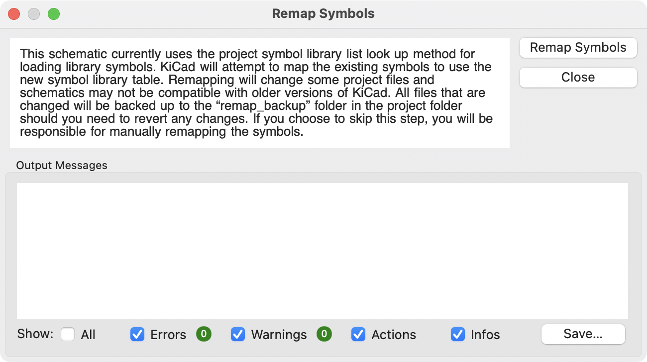
Hierarchical schematics
Introduction
In KiCad, multi-sheet schematics are hierarchical: there is a single root sheet, and additional sheets are created as subsheets of either the root sheet or another subsheet. Sheets can be included in a hierarchy multiple times, if desired.
Carefully drawing a schematic as a hierarchical design improves schematic legibility and reduces repetitive drawing.
Creating a hierarchical schematic starts from the root sheet. The process is to create a subsheet, then draw the circuit in the subsheet and make the necessary electrical connections between sheets. Connections can be made between nets in a subsheet and nets in the parent sheet using hierarchical pins and labels, or between any two nets in the hierarchy using global labels.
Adding sheets to a design
You can add a subsheet to a design with the Add Hierarchical Sheet tool
(S hotkey, or the
![]() button in the right toolbar). Launch the tool, then click twice in the canvas to
draw the upper left and lower right corners of the subsheet symbol. Make the
sheet outline large enough to fit the
hierarchical pins you will add later.
button in the right toolbar). Launch the tool, then click twice in the canvas to
draw the upper left and lower right corners of the subsheet symbol. Make the
sheet outline large enough to fit the
hierarchical pins you will add later.
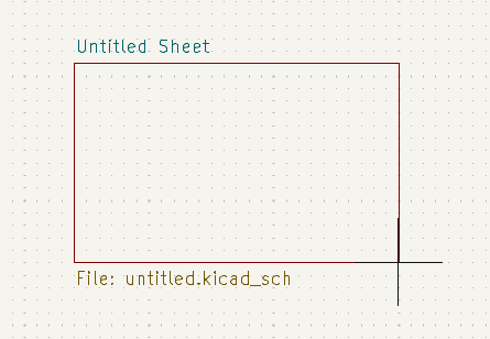
The Sheet Properties dialog will appear and prompt you for a sheet name and filename.
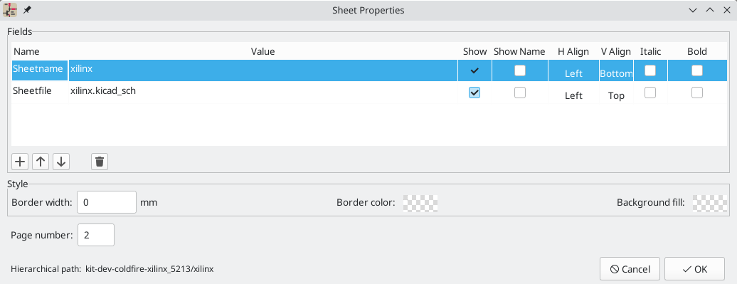
The sheet name must be unique, as it is used in the full net name for any nets
in the subsheet. For example, a net with the local label net1 in the sheet
sheet1 would have a full net name of /sheet1/net1. The sheet name is also
used to refer to the sheet in various places in the GUI, including the
title block and the
hierarchy navigator.
The sheet file specifies the file that the new sheet will be saved to or loaded from. The path to the sheet file can be relative or absolute. It is usually preferable to save subsheet files in the project directory and use a relative path so that the project is portable.
A single sheet file can be used more than once in a project by specifying the same filename for each repeated sheet; the circuit drawn in the sheet will be instantiated once per usage, and any edits in once instance will be reflected in the other instances.
| Sheet files can be shared between multiple projects to allow design reuse between projects. However, this is not recommended due to path portability concerns and the risk of unintentionally changing other projects while editing a shared sheet. |
The sheet’s page number is configurable here. The page number is displayed in the sheet title block and the hierarchy navigator, and sheets are sorted by page number in the hierarchy navigator and when printing or plotting.
Several graphical options are also available. Border width sets the width of the border around the sheet shape. Border color and Background fill set the color for the border and fill of the sheet shape, respectively. If no color is set, a checkerboard swatch is shown and the default values from the color theme are used.
Sheets support arbitrary custom fields, which can be added and removed with the
![]() and
and
![]() buttons, respectively. Sheet
fields can be optionally displayed on the schematic by checking their Show
box, and they can be accessed from inside the sheet or in other sheet fields
using text variables.
buttons, respectively. Sheet
fields can be optionally displayed on the schematic by checking their Show
box, and they can be accessed from inside the sheet or in other sheet fields
using text variables.
The Sheet Properties dialog can be accessed at any time by selecting a sheet symbol and using the E hotkey, or by right-clicking on a sheet symbol and selecting Properties….
Navigating between sheets
You can enter a hierarchical sheet from the parent sheet by double-clicking the child sheet’s shape, or right-clicking the child sheet and selecting Enter Sheet.
Return to the parent sheet by using the
![]() button in the top toolbar, or by
right-clicking in an empty part of the schematic and clicking Leave Sheet.
button in the top toolbar, or by
right-clicking in an empty part of the schematic and clicking Leave Sheet.
You can jump to the next sheet with the
![]() button, or to the previous
sheet with the
button, or to the previous
sheet with the ![]() button.
button.
Alternatively, you can jump to any sheet with the hierarchy navigator. To open
the hierarchy navigator, click the
![]() button in the
left toolbar. The hierarchy navigator docks at the left of the screen. Each
sheet in the design is displayed as an item in the tree. Clicking a sheet name
opens that sheet in the editing canvas.
button in the
left toolbar. The hierarchy navigator docks at the left of the screen. Each
sheet in the design is displayed as an item in the tree. Clicking a sheet name
opens that sheet in the editing canvas.
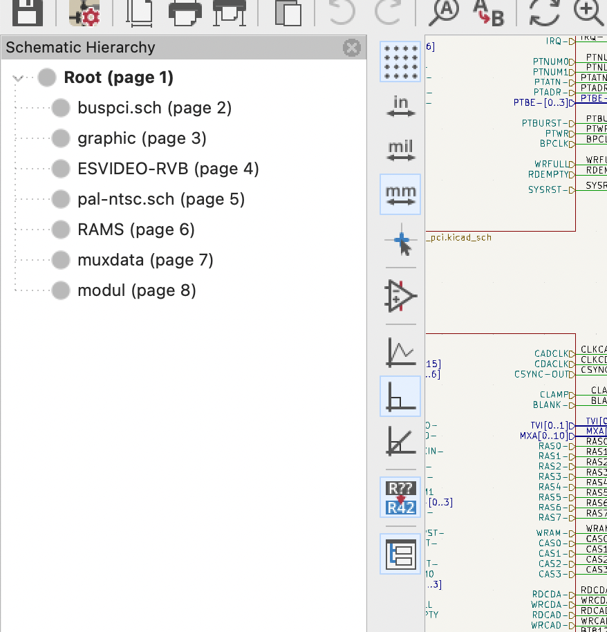
Electrical connections between sheets
Label overview
Electrical connections between sheets are made with labels. There are several kinds of labels in KiCad, each with a different connection scope.
-
Local labels only make connections within a sheet. Therefore local labels cannot be used to connect between sheets. Local labels are added with the
button. -
Global labels make connections anywhere in a schematic, regardless of sheet. Global labels are added with the
button. -
Hierarchical labels connect to hierarchical sheet pins accessible in the parent sheet. Hierarchical designs rely on hierarchical labels and pins to make connections between parent sheets and child sheets; you can think of hierarchical pins as defining the interface for a sheet. Hierarchical labels are added with the
button.
| Labels that have the same name will connect, regardless of the label type, if they are in the same sheet. |
| Hidden power pins can also be considered global labels, because they connect anywhere in the schematic hierarchy. |
Hierarchical sheet pins
After placing hierarchical labels within the subsheet, matching hierarchical pins can be added to the subsheet symbol in the parent sheet. You can then make connections to the hierarchical pins with wires, labels, and buses. Hierarchical pins in a subsheet symbol are connected to the matching hierarchical labels in the subsheet itself.
| Hierarchical labels must be defined in the subsheet before the corresponding hierarchical sheet pin can be imported in the sheet symbol. |
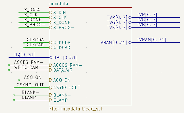
For every hierarchical label in the subsheet, import the corresponding
hierarchical pin into the sheet symbol by clicking the
![]() button in the right toolbar, then clicking on the sheet symbol. A sheet
pin for the first unmatched hierarchical label will be attached to the cursor,
where it can be placed anywhere along the border of the sheet symbol. Clicking
again with the tool will continue to import additional sheet pins until there
are no more hierarchical pins to import from the subsheet. Sheet pins can
also be imported by selecting Import Sheet Pin in a sheet symbol’s
right-click context menu.
button in the right toolbar, then clicking on the sheet symbol. A sheet
pin for the first unmatched hierarchical label will be attached to the cursor,
where it can be placed anywhere along the border of the sheet symbol. Clicking
again with the tool will continue to import additional sheet pins until there
are no more hierarchical pins to import from the subsheet. Sheet pins can
also be imported by selecting Import Sheet Pin in a sheet symbol’s
right-click context menu.
You can edit the properties of a sheet pin in the Sheet Pin Properties dialog. Open this dialog by double-clicking a sheet pin, selecting a sheet pin and using the E hotkey, or right-clicking a sheet pin and selecting Properties….
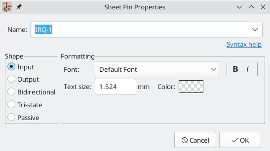
The sheet pin’s name can be edited in the textbox or by selecting from the dropdown list of hierarchical labels in the subsheet. A sheet pin’s name has to match the corresponding hierarchical label in the subsheet, so if a pin name is changed the label must change as well.
Shape changes the shape of the sheet pin, and has no electrical effect. It can be set to Input, Output, Bidirectional, Tri-state, or Passive. The pin’s font, text size, color, and emphasis (bold or italic) can also be changed.
Hierarchical design examples
Hierarchical designs can be put into one of several categories:
-
Simple: each sheet is used only once.
-
Complex: some sheets are instantiated multiple times.
-
Flat: a sub-case of a simple hierarchy, without connections between subsheets and their parent. Flat hierarchies can be used to represent a non-hierarchical design.
Each hierarchy model can be useful; the most appropriate one depends on the design.
Simple hierarchy
An example of a simple hierarchy is the video demo project included with
KiCad. The root sheet contains seven unique subsheets, each with hierarchical
labels and sheet pins linking the sheets to each other in the root sheet. Two of
the subsheet symbols are shown below.
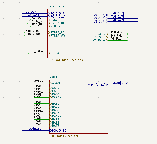
Complex Hierarchy
The complex_hierarchy demo project is an example of a complex hierarchy.
The root sheet contains two subsheet symbols, which both refer to the same sheet
file (ampli_ht.kicad_sch). This allows the design to include two copies of the
same amplifier circuit. Although the two sheet symbols refer to the same
filename, the sheet names are unique (ampli_ht_vertical and
ampli_ht_horizontal). Inside each subsheet the circuits are identical except
for the reference designators, which as always are unique.
This project contains no sheet pin connections. The only connections between the root sheet and the subsheets are global power connections made with power symbols. However, sheets in a complex hierarchy could include sheet pin connections if appropriate for the design.
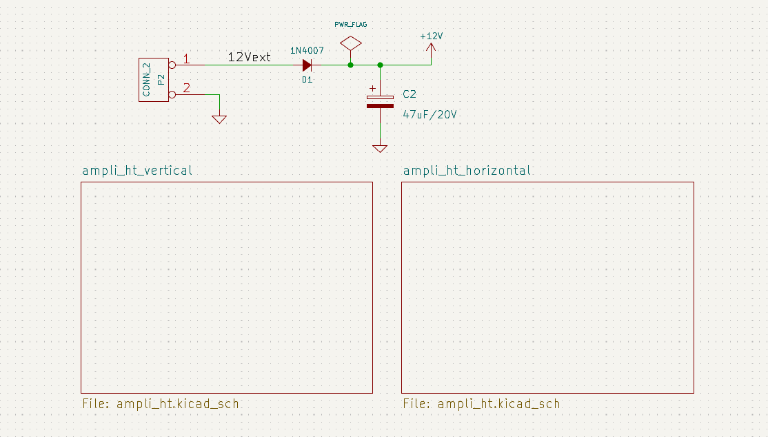
Flat hierarchy
The flat_hierarchy demo project is an example of a flat hierarchy. The root
sheet contains two unique subsheet symbols with no hierarchical sheet pins. The
root sheet in this project does nothing except hold the subsheets, and the
subsheets are used only as additional pages in the schematic.
| This is the simplest way to create multi-page schematics in KiCad. |
Inspecting a schematic
Find tool
The Find tool searches for text in the schematic, including reference
designators, pin names, symbol fields, and graphic text. When the tool finds a
match, the canvas is zoomed and centered on the match and the text is
highlighted. Launch the tool using the ![]() button in the top toolbar.
button in the top toolbar.
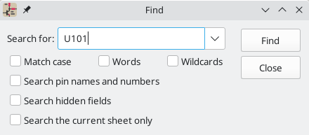
The Find tool has several options:
Match case: Selects whether the search is case-sensitive.
Words: When selected, the search will only match the search term with complete words in the schematic. When unselected, the search will match if the search term is part of a larger word in the schematic.
Wildcards: When selected, wildcards can be used in the search terms. ?
matches any single character, and * matches any number of characters. Note
that when this option is selected, partial matches are not returned: searching
for abc* will match the string abcd, but searching for abc will not.
Search pin names and numbers: Selects whether the search should apply to pin names and numbers.
Search hidden fields: Selects whether the search should apply only to visible fields or if it should include hidden symbol fields.
Search the current sheet only: Selects whether the search should be limited to the current schematic sheet or to the entire schematic.
There is also a Find and Replace tool which is activated with the
![]() button in the top
toolbar. This tool behaves the same as the Find tool, but additionally can
replace some or all matches with different text.
button in the top
toolbar. This tool behaves the same as the Find tool, but additionally can
replace some or all matches with different text.
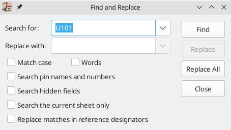
If the Replace matches in reference designators option is checked, reference designators will be modified if they contain matching text. Otherwise reference designators will not be affected.
Net highlighting
An electrical net can be highlighted in the schematic editor to visualize all of the places it appears in the schematic. Net highlighting can be activated in the Schematic Editor or by highlighting the corresponding net in the PCB editor when cross-probe highlighting is enabled (see below). When net highlighting is active, the highlighted net will be shown in a different color. By default this color is pink, but it is configurable in the Color section of the Preferences dialog.
Nets can be highlighted by clicking on a wire or pin using the Highlight Net
tool in the right toolbar (![]() ). Alternatively, the Highlight Net hotkey (`) highlights
the net under the cursor.
). Alternatively, the Highlight Net hotkey (`) highlights
the net under the cursor.
Net highlighting can be cleared by using the Clear Net Highlight action (hotkey ~) or by using the Highlight net tool on an empty region in the schematic. By default, Esc also clears net highlighting, but this can be disabled if desired in Preferences → Schematic Editor → Editing Options.
Cross-probing from the PCB
KiCad allows bi-directional cross-probing between the schematic and the PCB. There are several different types of cross-probing.
Selection cross-probing allows you to select a symbol or pin in the schematic to select the corresponding footprint or pad in the PCB (if one exists) and vice-versa. By default, cross-probing will result in the display centering on the cross-probed item and zooming to fit. This behavior can be disabled in the Display Options section of the Preferences dialog.
Highlight cross-probing allows you to highlight a net in the schematic and PCB at the same time. If the option "Highlight cross-probed nets" is enabled in the Display Options section of the Preferences dialog, highlighting a net or bus in the schematic editor will cause the corresponding net or nets to be highlighted in the PCB editor, and vice versa.
Electrical Rules Check
The Electrical Rules Check (ERC) tool checks for certain errors in your schematic, such as unconnected pins, unconnected hierarchical symbols, shorted outputs or other illegal connections, etc. ERC violations are reported as errors or warnings depending on the severity of the issue detected.
ERC is imperfect and cannot detect all errors, but it can detect many common issues and oversights. All detected issues should be checked and addressed before proceeding. The quality of the ERC is directly related to the care taken in declaring electrical pin properties during symbol creation. If symbols are designed incorrectly, ERC will not report accurate information.
ERC can be started by clicking on the
![]() button in the top toolbar and clicking
the Run ERC button.
button in the top toolbar and clicking
the Run ERC button.
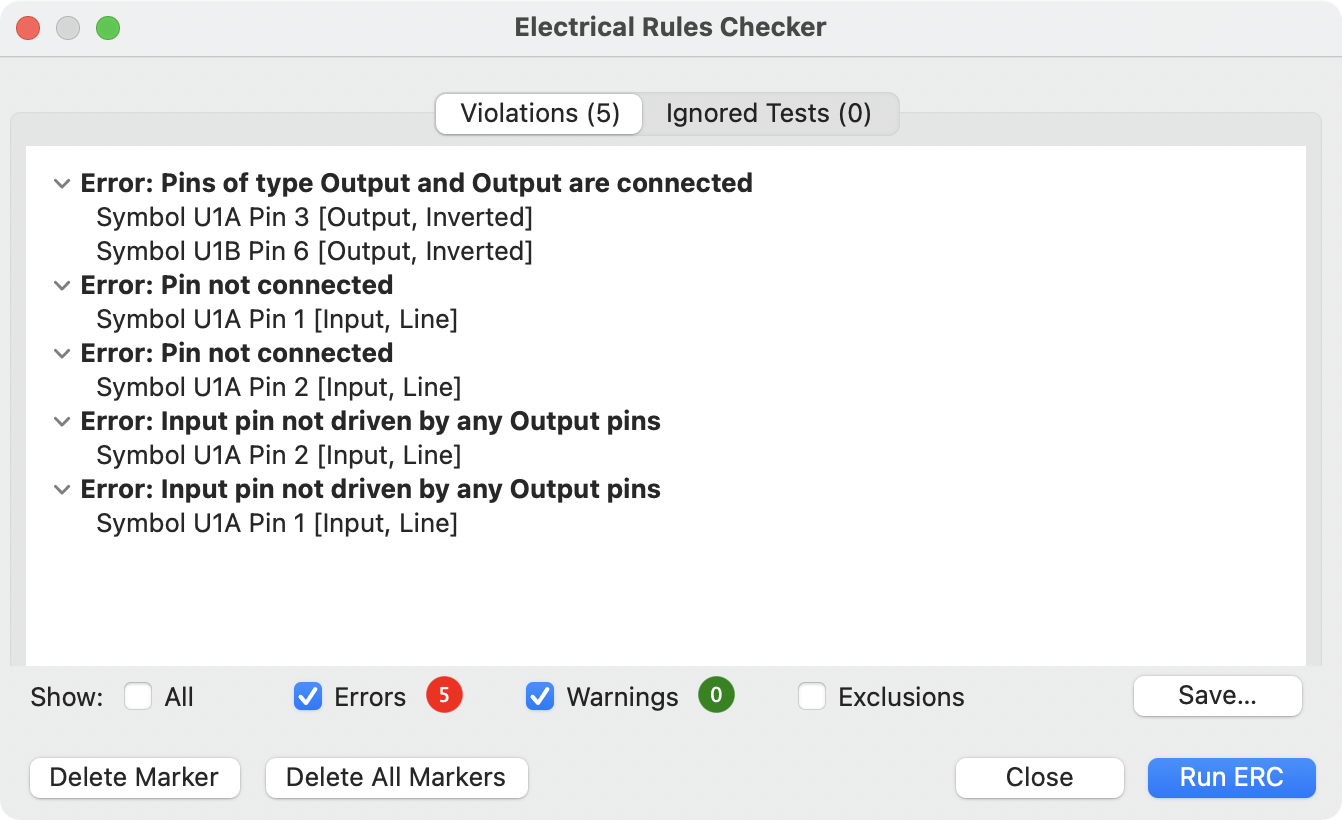
Any warnings or errors are reported in the Violations tab, and markers for each violation are placed in the schematic so that they point to the relevant part of the schematic. Warnings are indicated by yellow arrows, and errors have red arrows. Excluded violations are shown as green arrows.
| Selecting a violation in the ERC window jumps to the selected violation marker in the schematic. |
The numbers at the bottom of the window show the number of errors, warnings, and exclusions. Each type of violation can be filtered from the list using the respective checkboxes. Clicking Delete Markers will clear all violations until ERC is run again.
Violations can be right-clicked in the dialog to ignore them or change their severity:
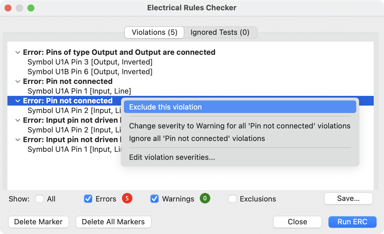
-
Exclude this violation: ignores this particular violation, but does not affect any other violations.
-
Change severity: changes a type of violation from warning to error, or error to warning. This affects all violations of a given type.
-
Ignore all: ignores all violations of a given type. This test will now appear in the Ignored Tests tab rather than the Violations tab.
You can also exclude the selected marker with Inspect → Exclude Marker, and show or hide each category of marker (errors, warnings, and exclusions) with the View menu.
Excluded and ignored violations are remembered between runs of the design rule checker.
ERC example
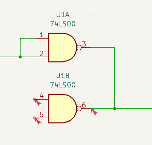
There are three errors in the screenshot above.
-
Two outputs have been connected together (red arrow at right).
-
Two inputs have been left unconnected (red arrows at left). This is actually two errors per pin: each pin is unconnected, and each pin is an input pin that is not driven by an output pin.
Selecting an ERC marker displays a description of the violation in the message pane at the bottom of the window.
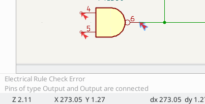
Power pins and power flags
It is common to have an "Input Power pin not driven by any Output Power pins" error on power pins, as shown in the example below, even though the power pins seem to be properly connected to a power rail. This happens in designs where the power is provided through connectors or other components that are not marked as power outputs. In these cases ERC won’t detect any Output Power pins connected to the net and will determine the Input Power pin is not driven by a power source.
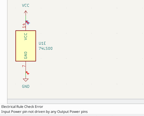
To avoid this warning, connect the net to PWR_FLAG symbol on such a power net
as shown in the following example. The PWR_FLAG symbol is found in the power
symbol library. Alternatively, connect any power output pin to the net;
PWR_FLAG is simply a symbol with a single power output pin.
Ground nets often need a PWR_FLAG as well, because voltage regulators have
outputs declared as power outputs, but their ground pins are typically marked as
power inputs. Therefore grounds can appear unconnected to a source unless a
PWR_FLAG symbol is used.
For more information about power pins and power flags, see the
PWR_FLAG documentation.
ERC Configuration
The Violation Severity panel in Schematic Setup lets you configure what types of ERC messages should be reported as Errors, Warnings, or ignored.
The Pin Conflicts Map panel in Schematic Setup allows you to configure connectivity rules to define electrical conditions for errors and warnings based on what types of pins are connected to each other. For example, by default an error is produced when an output pin is connected to another output pin.
Rules can be changed by clicking on the desired square of the matrix, causing it to cycle through the choices: allowed, warning, error.
List of ERC checks
The table below lists the electrical rules that KiCad checks and the default violation severity for each check. All severities are configurable.
| Violation | Description | Default Severity |
|---|---|---|
Pin not connected |
All symbol pins must be connected to a net, unless the pin has a no-connect flag or has electrical type Unconnected. |
Error |
Input pin not driven by any Output pins |
All Input pins must be connected to an Output pin. |
Error |
Input Power pin not driven by any Output Power pins |
All Input Power pins must be connected to an Output Power pin. A common cause of this violation is described above. |
Error |
A pin with a "no connection" flag is connected |
Pins with no connection flags cannot be connected to anything else. |
Warning |
Unconnected "no connection" flag |
No connection flags cannot be left unconnected. They must be connected to a pin or label. |
Warning |
Label not connected to anything |
Global, hierarchical, and local labels must be connected to a pin or another label. |
Error |
Global label not connected anywhere else in the schematic |
Global labels need at least two other pins on the same net; otherwise they are not connecting anything. |
Warning |
Wires not connected to anything |
Wires must be connected to a pin or label. |
Error |
Bus Entry needed |
This violation only applies to projects imported from EAGLE projects. It indicates places where the importer was unable to automatically add bus entries to the imported schematic, so you must add them by hand. |
Error |
Symbol pin or wire end off grid |
Symbol pins and wire ends need to be aligned to the grid in order to connect to each other. |
Warning |
Duplicate reference designators |
Two symbols cannot have the same reference designator. |
Error |
Units of same symbol have different values |
All units of a single symbol must have the same value. |
Error |
Different footprint assigned in another unit of the symbol |
All units of a single symbol must have the same footprint assigned. |
Error |
Different net assigned to a shared pin in another unit of the symbol |
Any pins that are shared between multiple units of a symbol must have the same net connected across all units. |
Error |
Duplicate sheet names within a given sheet |
All hierarchical sheets within a given sheet must have unique names. |
Error |
Mismatch between hierarchical labels and sheet pins |
All hierarchical labels must have a corresponding hierarchical sheet pin in the parent sheet, and all hierarchical sheet pins must have a matching hierarchical label in the child sheet. |
Error |
More than one name given given to this bus or net |
Nets can only have a single name, so if multiple labels are attached to a net, one name will be selected and used as the canonical name. |
Warning |
Conflict between bus alias definitions across schematic sheets |
If the same bus alias name is used in multiple sheets, the members of the alias must be the same for each sheet. |
Error |
Buses are graphically connected but share no bus members |
Buses that are graphically connected must have bus members in common. |
Error |
Invalid connection between bus and net items |
Buses cannot be connected to net items such as wires, labels referring to single nets, or sheet pins referring to single nets. Labels and sheet pins can only be connected to buses if they refer to buses rather than individual signals. |
Error |
Net is graphically connected to a bus but not a bus member |
Nets can only be connected to a bus with a bus entry if they are a member of the bus. |
Warning |
Conflicting netclass assignments |
Only one netclass can be assigned to a net. |
Error |
Symbol is not annotated |
Symbols must be annotated with a unique reference designator. |
Error |
Unresolved text variable |
Text variables ( |
Error |
SPICE model issue |
SPICE models must not have syntax errors or other problems. |
Error |
Labels are similar (lower/upper case difference only) |
If two labels are similar and differ only by the case of some letters, this may be a typo causing two labels to be disconnected when they are intended to be connected. |
Warning |
Library symbol issue |
Several symbol library issues are checked:
|
Warning |
Symbol has more units than are defined |
Symbols cannot have more units placed in the schematic than are defined in the symbol. Units in the schematic must correspond exactly to the symbol definition. |
Error |
Symbol has units that are not placed |
All of the units in a multi-unit symbol should be placed in the schematic. |
Warning |
Symbol has input pins that are not placed |
A multi-unit symbol has units with input pins that are not placed, so those input pins will not be connected to anything. All units with input pins should be placed in the schematic. |
Warning |
Symbol has bidirectional pins that are not placed |
A multi-unit symbol has units with bidirectional pins that are not placed, so those bidirectional pins will not be connected to anything. All units with bidirectional pins should be placed in the schematic. |
Warning |
Symbol has power input pins that are not placed |
A multi-unit symbol has units with power input pins that are not placed, so those power input pins will not be connected to anything. All units with power input pins should be placed in the schematic. |
Error |
Conflict problem between pins |
Connections between pins must match the allowed connections in the Pin Conflicts Map. |
From Pin Conflicts Map |
ERC report file
An ERC report file can be generated and saved by clicking the Save… button
in the ERC dialog. The file extension for ERC report files is .rpt. An example
ERC report file is given below.
ERC report (Fri 21 Oct 2022 02:07:05 PM EDT, Encoding UTF8)

***** Sheet /
[pin_not_driven]: Input pin not driven by any Output pins
    ; Severity: error
    @(149.86 mm, 60.96 mm): Symbol U1B [74LS00] Pin 4 [, Input, Line]
[pin_not_connected]: Pin not connected
    ; Severity: error
    @(149.86 mm, 60.96 mm): Symbol U1B [74LS00] Pin 4 [, Input, Line]
[pin_not_connected]: Pin not connected
    ; Severity: error
    @(149.86 mm, 66.04 mm): Symbol U1B [74LS00] Pin 5 [, Input, Line]
[pin_to_pin]: Pins of type Output and Output are connected
    ; Severity: error
    @(165.10 mm, 63.50 mm): Symbol U1B [74LS00] Pin 6 [, Output, Inverted]
    @(165.10 mm, 46.99 mm): Symbol U1A [74LS00] Pin 3 [, Output, Inverted]
[pin_not_driven]: Input pin not driven by any Output pins
    ; Severity: error
    @(149.86 mm, 66.04 mm): Symbol U1B [74LS00] Pin 5 [, Input, Line]

 ** ERC messages: 5  Errors 5  Warnings 0
Assigning Footprints
Before routing a PCB, footprints need to be selected for every component that will be assembled on the board. Footprints define the copper connections between physical components and the routed traces on a circuit board.
Some symbols come with footprints pre-assigned, but for many symbols there are multiple possible footprints, so the user needs to select the appropriate one.
KiCad offers several ways to assign footprints:
-
Symbol Properties
-
Symbol Properties Dialog
-
Symbol Fields Table
-
-
While placing symbols
-
Footprint Assignment Tool
Each method will be explained below. Which to use is a matter of preference;
one method may be more convenient depending on the situation. All of these
methods are equivalent in that they store the name of the selected footprint in
the symbol’s Footprint field.
| The Footprint Library Table needs to be configured before footprints can be assigned. For information on configuring the Footprint Library Table, please see the PCB Editor manual. |
Assigning Footprints in Symbol Properties
A symbol’s Footprint field can be edited directly in the symbol’s Properties window.
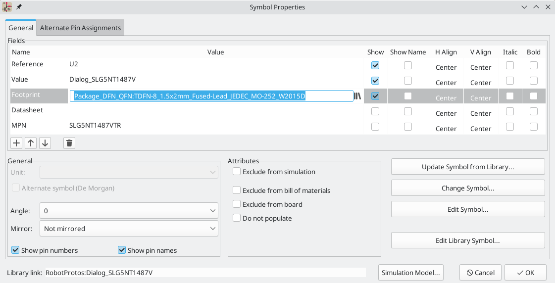
Clicking the ![]() button in the
button in the
Footprint field opens the Footprint Library Browser, which shows the available
footprints and footprint libraries. Single clicking a footprint name selects the
footprint and displays it in the preview pane on the right, while double
clicking on a footprint closes the browser and sets the symbol’s Footprint
field to the selected footprint.
Assigning Footprints with the Symbol Fields Table
Rather than editing the properties of each symbol individually, the Symbol
Fields Table can be used to view and edit the properties of all symbols in the
design in one place. This includes assigning footprints by editing the
Footprint field of each symbol.
The Symbol Fields Table is accessed with Tools → Edit Symbol Fields…,
or with the ![]() button on the top toolbar.
button on the top toolbar.
The Footprint field behaves the same here as in the Symbol Properties window:
it can be edited directly, or footprints can be selected visually with the
Footprint Library Browser.
For more information on the Symbol Fields Table, see the section on editing symbol properties.
Assigning Footprints While Placing Symbols
Footprints can be assigned to symbols when the symbol is first added to the schematic.
Some symbols are defined with a default footprint. These symbols will have this footprint preassigned when they are added to the schematic. The default footprint is shown in the Add Symbol dialog. For symbols without a default symbol defined, the footprint dropdown will say "No default footprint", and the footprint preview canvas will say "No footprint specified".
Symbols can have footprint filters that specify which footprints are appropriate to use with that symbol. If footprint filters are defined for the selected symbol, all footprints that match the footprint filters will appear as options in the footprint dropdown. The selected footprint will be displayed in the preview canvas and will be assigned to the symbol when the symbol is added to the schematic.
| Footprint options will not appear in the footprint dropdown unless the footprint libraries are loaded. Footprint libraries are loaded the first time the Footprint Editor or Footprint Library Browser are opened in a session. |
For more information on footprint filters, see the Symbol Editor Documentation.
Assigning Footprints with the Footprint Assignment Tool
The Footprint Assignment Tool allows you to associate symbols in your schematic to footprints used when laying out the printed circuit board. It provides footprint list filtering, footprint viewing, and 3D component model viewing to help ensure the correct footprint is associated with each component.
Components can be assigned to their corresponding footprints manually or automatically by creating equivalence files (.equ files). Equivalence files are lookup tables associating each component with its footprint.
Run the tool with Tools → Assign Footprints…, or by clicking the
![]() icon
in the top toolbar.
icon
in the top toolbar.
Footprint Assignment Tool Overview
The image below shows the main window of the Footprint Assignment Tool.
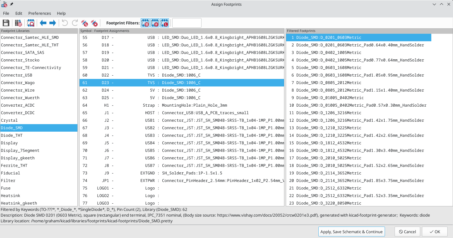
-
The left pane contains the list of available footprint libraries associated with the project.
-
The center pane contains the list of symbols in the schematic.
-
The right pane contains the list of available footprints loaded from the project footprint libraries.
-
The bottom pane describes the filters that have been applied to the footprint list and prints information about the footprint selected in the rightmost pane.
The top toolbar contains the following commands:
|
Transfer the current footprint associations to the schematic. |
|
Edit the global and project footprint library tables. |
|
View the selected footprint in the footprint viewer. |
|
Select the previous symbol without a footprint association. |
|
Select the next symbol without a footprint association. |
|
Undo last edit. |
|
Redo last edit. |
|
Perform automatic footprint association using an equivalence file. |
|
Delete all footprint assignments. |
|
Filter footprint list by footprint filters defined in the selected symbol. |
|
Filter footprint list by pin count of the selected symbol. |
|
Filter footprint list by selected library. |
The following table lists the keyboard commands for the Footprint Assignment Tool:
Right Arrow / Tab |
Activate the pane to the right of the currently activated pane. Wrap around to the first pane if the last pane is currently activated. |
Left Arrow |
Activate the pane to the left of the currently activated pane. Wrap around to the last pane if the first pane is currently activated. |
Up Arrow |
Select the previous item of the currently selected list. |
Down Arrow |
Select the next item of the currently selected list. |
Page Up |
Select the item one full page upwards of the currently selected item. |
Page Down |
Select the item one full page downwards of the currently selected item. |
Home |
Select the first item of the currently selected list. |
End |
Select the last item of the currently selected list. |
Manually Assigning Footprints with the Footprint Assignment Tool
To manually associate a footprint with a component, first select a component in the component (middle) pane. Then select a footprint in the footprint (right) pane by double-clicking on the name of the desired footprint. The footprint will be assigned to the selected component, and the next component without an assigned footprint is automatically selected.
| If no footprints appear in the footprint pane, check that the footprint filter options are correctly applied. |
When all components have footprints assigned to them, click the OK button to save the assignments and exit the tool. Alternatively, click Cancel to discard the updated assignments, or Apply, Save Schematic & Continue to save the new assignments without exiting the tool.
Filtering the Footprint List
There are four filtering options which restrict which footprints are displayed in the footprint pane. The filtering options are enabled and disabled with three buttons and a textbox in the top toolbar.
-
 : Activate
filters that can be defined in each symbol.
For example, an opamp symbol might define filters that show only SOIC and DIP
footprints.
: Activate
filters that can be defined in each symbol.
For example, an opamp symbol might define filters that show only SOIC and DIP
footprints. -
 : Only show footprints
that match the selected symbol’s pin count.
: Only show footprints
that match the selected symbol’s pin count. -
 : Only show footprints from the
library selected in the left pane.
: Only show footprints from the
library selected in the left pane. -
Entering text in the textbox hides footprints that do not match the text. This filter is disabled when the box is empty.
When all filters are disabled, the full footprint list is shown.
The applied filters are described in the bottom pane of the window, along with the number of footprints that meet the selected filters. For example, when the symbol’s footprint filters and pin count filters are enabled, the bottom pane prints the footprint filters and pin count:
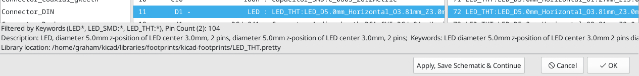
Multiple filters can be used at once to help narrow down the list of possibly appropriate footprints in the footprint pane. The symbols in KiCad’s standard library define footprint filters that are designed to be used in combination with the pin count filter.
Automatically Assigning Footprints with the Footprint Assignment Tool
The Footprint Assignment Tool allows you to store footprint assignments in an external file and load the assignments later, even in a different project. This allows you to automatically associate symbols with the appropriate footprints.
The external file is referred to as an equivalence file, and it stores a mapping
of a symbol value to a corresponding footprint. Equivalence files typically use
the .equ file extension. Equivalence files are plain text files with a simple
syntax, and must be created by the user using a text editor. The syntax is
described below.
You can select which equivalence files to use by clicking Preferences → Manage Footprint Association Files in the Footprint Assignment Tool.
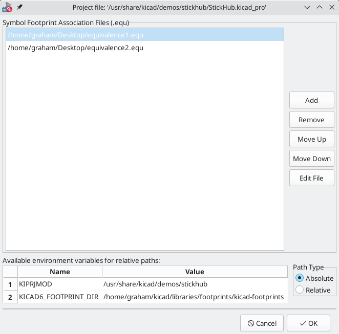
-
Add new equivalence files by clicking the Add button.
-
Remove the selected equivalence file by clicking the Remove button.
-
Change the priority of equivalence files by clicking the Move Up and Move Down buttons. If a symbol’s value is found in multiple equivalence files, the footprint from the last matching equivalence file will override earlier equivalence files.
-
Open the selected equivalence file by clicking the Edit File button.
Relevant environment variables are shown at the bottom of the window. When the Relative path option is checked, these environment variables will automatically be used to make paths to selected equivalence files relative to the project or footprint libraries.
Once the desired equivalence files have been loaded in the correct order,
automatic footprint association can be performed by clicking the
![]() button in the top toolbar of the Footprint Assignment Tool.
button in the top toolbar of the Footprint Assignment Tool.
All symbols with a value found in a loaded equivalence file will have their footprints automatically assigned. However, symbols that already have footprints assigned will not be updated.
Equivalence File Format
Equivalence files consist of one line for each symbol value. Each line has the following structure:
'<symbol value>' '<footprint library>:<footprint name>'
Each name/value must be surrounded by single quotes (') and separated by one
or more spaces. Lines starting with # are comments.
For example, if you want all symbols with the value LM4562 to be assigned the
footprint Package_SO:SOIC-8_3.9x4.9_P1.27mm, the line in the equivalence file
should be:
'LM4562' 'Package_SO:SOIC-8_3.9x4.9_P1.27mm'
Here is an example equivalence file:
#integrated circuits (smd):
'74LV14' 'Package_SO:SOIC-14_3.9x8.7mm_P1.27mm'
'EL7242C' 'Package_SO:SOIC-8_3.9x4.9_P1.27mm'
'DS1302N' 'Package_SO:SOIC-8_3.9x4.9_P1.27mm'
'LM324N' 'Package_SO:SOIC-14_3.9x8.7mm_P1.27mm'
'LM358' 'Package_SO:SOIC-8_3.9x4.9_P1.27mm'
'LTC1878' 'Package_SO:MSOP-8_3x3mm_P0.65mm'
'24LC512I/SM' 'Package_SO:SOIC-8_3.9x4.9_P1.27mm'
'LM2903M' 'Package_SO:SOIC-8_3.9x4.9_P1.27mm'
'LT1129_SO8' 'Package_SO:SOIC-8_3.9x4.9_P1.27mm'
'LT1129CS8-3.3' 'Package_SO:SOIC-8_3.9x4.9_P1.27mm'
'LT1129CS8' 'Package_SO:SOIC-8_3.9x4.9_P1.27mm'
'LM358M' 'Package_SO:SOIC-8_3.9x4.9_P1.27mm'
'TL7702BID' 'Package_SO:SOIC-8_3.9x4.9_P1.27mm'
'TL7702BCD' 'Package_SO:SOIC-8_3.9x4.9_P1.27mm'
'U2270B' 'Package_SO:SOIC-16_3.9x9.9_P1.27mm'

#regulators
'LP2985LV' 'Package_TO_SOT_SMD:SOT-23-5_HandSoldering'
Viewing the Current Footprint
The Footprint Assignment Tool contains a footprint viewer. Clicking the
![]() button
in the top toolbar launches the footprint viewer and shows the selected
footprint.
button
in the top toolbar launches the footprint viewer and shows the selected
footprint.
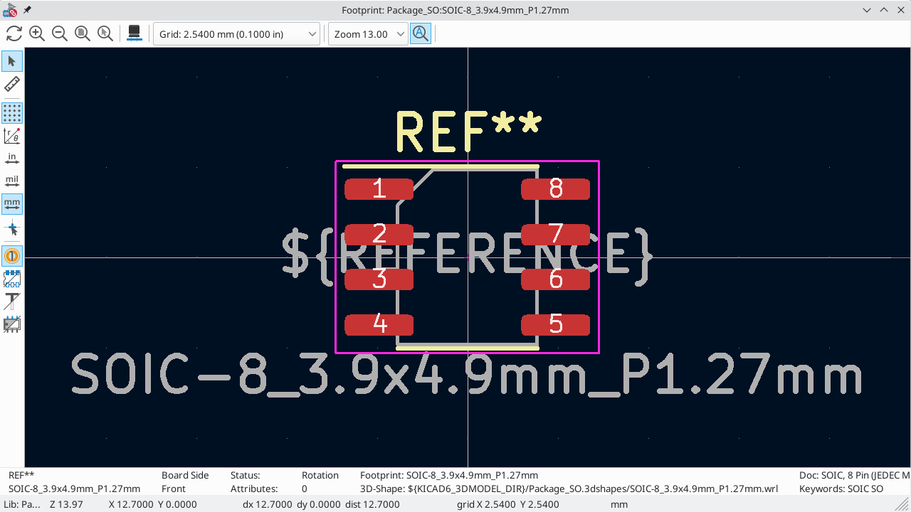
The top toolbar contains the following commands:
|
Refresh view |
|
Zoom in |
|
Zoom out |
|
Zoom to fit drawing in display area |
|
Show 3D viewer |
The left toolbar contains the following commands:
|
Use the select tool |
|
Interactively measure between two points |
|
Display grid dots or lines |
|
Switch between polar and cartesian coordinate systems |
|
Use inches |
|
Display coordinates in mils (1/1000 of an inch) |
|
Display coordinates in millimeters |
|
Toggle display of full-window crosshairs |
|
Toggle between drawing pads in sketch or normal mode |
|
Toggle between drawing pads in normal mode or outline mode |
|
Toggle between drawing text in normal mode or outline mode |
|
Toggle between drawing graphic lines in normal mode or outline mode |
Viewing the Current 3D Model
Clicking the ![]() button opens the
footprint in the 3D model viewer.
button opens the
footprint in the 3D model viewer.
| If a 3D model does not exist for the current footprint, only the footprint itself will be shown in the 3D Viewer. |
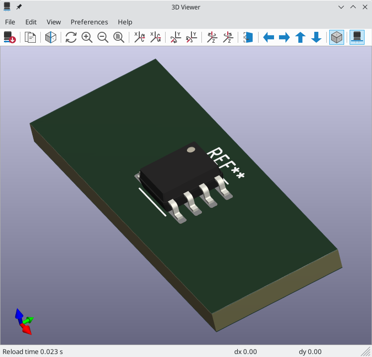
The 3D Viewer is described in the PCB Editor manual.
Forward and back annotation
Update PCB from Schematic (forward annotation)
Use the Update PCB from Schematic tool to sync design information from the
Schematic Editor to the Board Editor. The tool can be accessed with Tools →
Update PCB from Schematic (F8) in both the schematic and board
editors. You can also use the
![]() icon in the top toolbar of the Board Editor. This process is often called
forward annotation.
icon in the top toolbar of the Board Editor. This process is often called
forward annotation.
| Update PCB from Schematic is the preferred way to transfer design information from the schematic to the PCB. In older versions of KiCad, the equivalent process was to export a netlist from the Schematic Editor and import it into the Board Editor. It is no longer necessary to use a netlist file. |
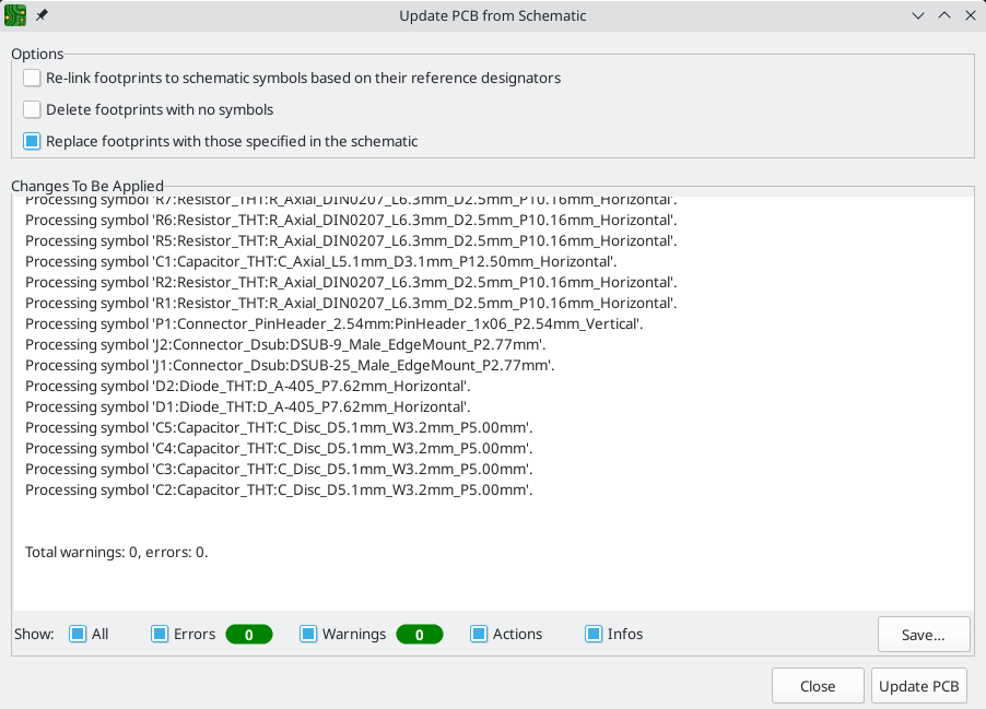
The tool adds the footprint for each symbol to the board and transfers updated schematic information to the board. In particular, the board’s net connections are updated to match the schematic. Symbols with the Exclude from board attribute are not transferred to the PCB.
The changes that will be made to the PCB are listed in the Changes To Be Applied pane. The PCB is not modified until you click the Update PCB button.
You can show or hide different types of messages using the checkboxes at the bottom of the window. A report of the changes can be saved to a file using the Save… button.
Options
The tool has several options to control its behavior.
| Option | Description |
|---|---|
Re-link footprints to schematic symbols based on their reference designators |
Footprints are normally linked to schematic symbols via a unique identifier created when the symbol is added to the schematic. A symbol’s unique identifier cannot be changed. If checked, each footprint in the PCB will be re-linked to the symbol that has the same reference designator as the footprint. If unchecked, footprints and symbols will be linked by unique identifier as usual, rather than by reference designator. Each footprint’s reference designator will be updated to match the reference designator of its linked symbol. This option should generally be left unchecked. It is useful for specific workflows that rely on changing the links between schematic symbols and footprints, such as refactoring a schematic for easier layout or replicating layout between identical channels of a design. |
Delete footprints with no symbols |
If checked, any footprint in the PCB without a corresponding symbol in the schematic will be deleted from the PCB. Footprints with the "Not in schematic" attribute will be unaffected. If unchecked, footprints without a corresponding symbol will not be deleted. |
Replace footprints with those specified in the schematic |
If checked, footprints in the PCB will be replaced with the footprint that is specified in the corresponding schematic symbol. If unchecked, footprints that are already in the PCB will not be changed, even if the schematic symbol is updated to specify a different footprint. |
Update Schematic from PCB (back annotation)
The typical workflow in KiCad is to make changes in the schematic and then sync the changes to the board using the Update PCB From Schematic tool. However, the reverse process is also possible: design changes can be made in the board and then synced back to the schematic using Tools → Update Schematic From PCB in either the schematic or board editors. This process is also known as backannotation.
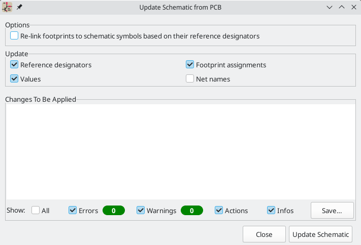
The tool syncs changes in reference designators, values, footprint assignments, and net names from the board to the schematic. Each type of change can be individually enabled or disabled.
The changes that will be made to the schematic are listed in the Changes To Be Applied pane. The schematic is not modified until you click the Update Schematic button.
You can show or hide different types of messages using the checkboxes at the bottom of the window. A report of the changes can be saved to a file using the Save… button.
Options
The tool has several options to control its behavior.
Option |
Description |
Re-link footprints to schematic symbols based on their reference designators |
If checked, each footprint in the PCB will be re-linked to the symbol that has the same reference designator as the footprint. This option is incompatible with updating symbol reference designators. If unchecked, footprints and symbols will be linked by unique identifier as usual, rather than by reference designator. |
Reference designators |
If checked, symbol reference designators will be updated to match the reference designators of the linked footprints. If unchecked, symbol reference designators will not be updated. |
Values |
If checked, symbol values will be updated to match the values of the linked footprints. If unchecked, symbol values will not be updated. |
Footprint assignments |
If checked, footprint assignments will be updated for symbols which have had their footprints changed or replaced in the board. If unchecked, symbol footprint assignments will not be updated. |
Net names |
If checked, the schematic will be updated with any net name changes that have been made in the board. Net labels will be updated or added to the schematic as necessary to match the board. If unchecked, net names will not be updated in the schematic. |
| The Geographical Reannotation feature can be used in combination with backannotating reference designators to reannotate all components in the design based on their location in the layout. |
Back annotation with CMP files
Select changes can also be synced from the PCB back to the schematic by exporting a CMP file from the PCB editor (File → Export → Footprint Association (.cmp) File…) and importing it in the Schematic Editor (File → Import → Footprint Assignments…).
| This method can only sync changes made to footprint assignments and footprint fields. It is recommended to use the Update Schematic from PCB tool instead. |
Generating Outputs
Printing
KiCad can print the schematic to a standard printer using File→Print….
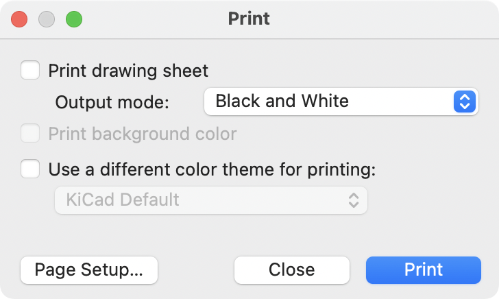
Printing options
Print drawing sheet: Include the drawing sheet border and title block in the printed schematic.
Output mode: Print the schematic in color or black and white.
Print background color: Include the background color in the printed schematic. This option is only enabled if Print in black and white only is disabled.
Use a different color theme for printing: Select a different color scheme for printing than the one selected for display in the Schematic Editor.
Page Setup…: Opens a page setup dialog for setting paper size and orientation.
Preview: Opens a print preview dialog.
Close: Closes the dialog without printing.
Print: Opens the system print dialog.
| Printing uses platform- and printer-specific drivers and may have unexpected results. When printing to a file, Plotting is recommended instead of Printing. |
Plotting
KiCad can plot schematics to a file using File → Plot….
The supported output formats are Postscript, PDF, SVG, DXF, and HPGL.
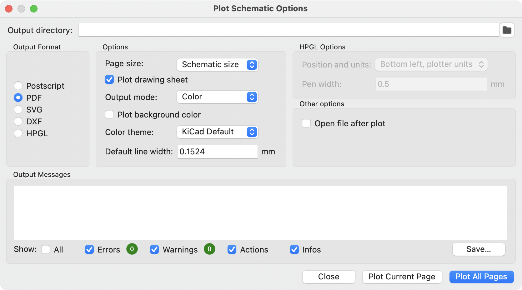
The Output Messages pane displays messages about the generated files. Different kinds of messages can be shown or hidden using the checkboxes, and the messages can be saved to a file using the Save… button.
The Plot Current Page button plots the current page of the schematic. The Plot All Pages button plots all pages of the schematic. One file is generated for each page, except for PDF output, which plots each schematic page as a separate page in a single PDF file.
Plotting options
Output directory: Specify the location to save plotted files. If this is a relative path, it is created relative to the project directory.
Output Format: Select the format to plot in. Some formats have different options than others.
Page size: Sets the page size to use for the plotted output. This can be set to match the schematic size or to another sheet size.
Plot drawing sheet: Include the drawing sheet border and title block in the printed schematic.
Output mode: Sets the output to color or black and white. Not all output formats support color.
Plot background color: Includes the schematic background color in the plotted output. The background color will not be plotted if the output format does not support color or the output mode is black and white.
Color theme: Selects the color theme to use for the plotted output.
Default line width: Selects the default width for lines without a specified thickness (lines that have thickness set to 0). Lines that have a set thickness will be plotted at that thickness instead.
Position and units: Sets the plotter origin and units. This option only applies for HPGL output.
Pen width: Sets the plotter’s pen width. This option only applies for HPGL output.
Open file after plot: automatically opens the plotted output file when plotting is complete.
Interactive PDF features
Plotted PDFs have several interactive features.
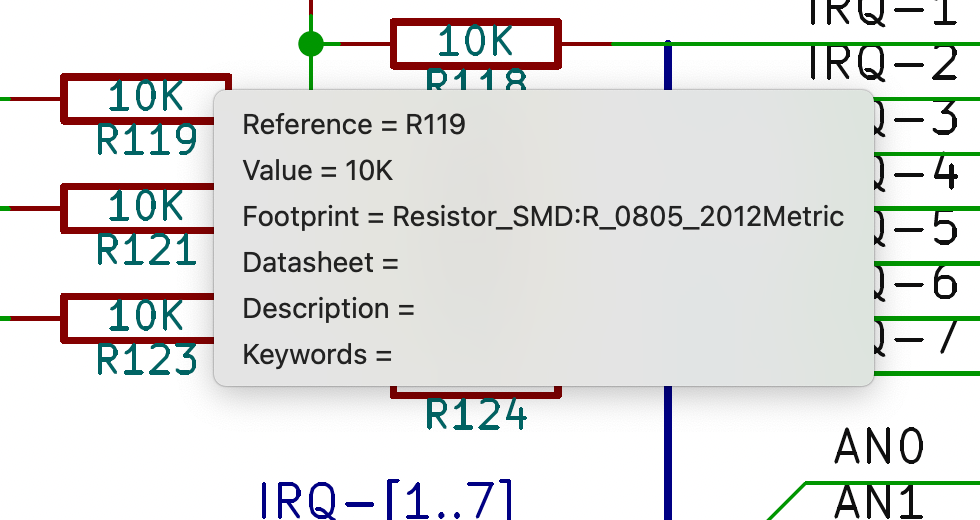
-
Hyperlinks can be clicked.
-
The table of contents is populated with schematic sheets as well as the symbols and hierarchical labels in each sheet.
-
Clicking on many schematic elements displays a popup menu containing relevant information.
-
Symbols display their symbol fields.
-
Hierarchical subsheets display their sheetname and filename, as well as an option to enter the sheet itself.
-
Labels display the resolved net and netclass.
-
Buses display their members.
-
| Some of these features are not supported in all PDF readers. |
Generating a Bill of Materials
KiCad can generate a Bill of Materials using Tools → Generate BOM… or
the ![]() button on the top toolbar. The
generated BOM lists all of the components in the design, except for components
with the Exclude from bill of materials
property set.
button on the top toolbar. The
generated BOM lists all of the components in the design, except for components
with the Exclude from bill of materials
property set.
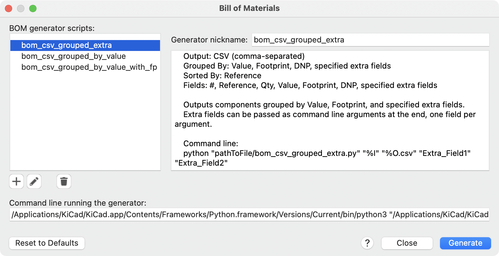
The BOM tool uses an external script to process the design information into the desired output format. Several BOM generator scripts are included with KiCad, and users can also create their own. BOM generator scripts generally use Python or XSLT, but other tools can be used as long as you can specify a command line for KiCad to execute when running the generator.
You can select which BOM generator to use in the BOM generator scripts list. The rest of the dialog displays information about the selected generator. You can change the displayed name of the generator with the Generator nickname textbox.
The pane at right displays information about the selected script. When the generator is executed, the right pane instead displays output from the script.
The text box at the bottom contains the command that KiCad will use to execute the generator. It is automatically populated when a script is selected, but the command may need to be hand-edited for some generators. KiCad saves the command line for each generator when the BOM tool is closed, so command line customizations are preserved. For more details about the command line, see the advanced documentation.
On Windows, the BOM Generator dialog has an additional option Show console window. When this option is unchecked, BOM generators run in a hidden console window and any output is redirected and printed in the dialog. When this option is checked, BOM generators run in a visible console window, which may be necessary if the generator plugin provides a graphical user interface.
BOM generator scripts
By default, the BOM tool presents three output script options.
-
bom_csv_grouped_extraoutputs a CSV with a single section containing every component in the design. Components are grouped by value, footprint, DNP (do not populate), and any additional fields that are specified on the command line. To specify extra fields, add the desired field names as quoted strings at the end of the command line. For example, to include theMPNfield, the end of the command line would be:<path to script>/bom_csv_grouped_extra.py "%I" "O.csv" "MPN". The columns in the BOM are:-
Line item number
-
Reference designator(s)
-
Quantity
-
Value
-
Footprint
-
DNP
-
Specified extra fields
-
-
bom_csv_grouped_by_valueoutputs a CSV with two sections. The first section contains every component in the design, with a single component on each line. The second section also contains every component, but components are grouped by symbol name, value, footprint, and DNP (do not populate). The columns in the BOM are:-
Line item number
-
Quantity
-
Reference designator(s)
-
Value
-
Symbol library and symbol name
-
Footprint
-
Datasheet
-
DNP
-
Any other symbol fields
-
-
bom_csv_grouped_by_value_with_fpoutputs a CSV with a single section containing every component in the design. Components are grouped by value, footprint, and DNP (do not populate). The columns in the BOM are:-
Reference designator(s)
-
Quantity
-
Value
-
Symbol name
-
Footprint
-
Symbol description
-
Vendor
-
DNP
-
Additional generator scripts are installed with KiCad but are not populated in the generator script list by default. The location of these scripts depends on the operating system and may vary based on installation location.
| Operating System | Location |
|---|---|
Windows |
|
Linux |
|
macOS |
|
Additional scripts can be added to the list of BOM generator scripts by clicking
the ![]() button. Scripts can be
removed by clicking the
button. Scripts can be
removed by clicking the ![]() button. The
button. The ![]() button opens the
selected script in a text editor.
button opens the
selected script in a text editor.
For more information on creating and using custom BOM generators, see the advanced documentation.
Other ways to generate a BOM
KiCad offers several additional ways to generate a BOM, although the BOM tool is recommended.
-
The Symbol Fields Table can export a CSV which can be used as a BOM. This option includes all symbol information but offers limited control over the output.
-
The PCB Editor can export a BOM through File → Fabrication Outputs → BOM…. This method provides no control over the output format and does not include all symbol information.
Generating a Netlist
A netlist is a file which describes electrical connections between symbol pins. These connections are referred to as nets. Netlist files contain:
-
A list of symbols and their pins.
-
A list of connections (nets) between symbol pins.
Many different netlist formats exist. Sometimes the symbols list and the list of nets are two separate files. This netlist is fundamental in the use of schematic capture software, because the netlist is the link with other electronic CAD software, such as PCB layout software, simulators, and programmable logic compilers.
KiCad supports several netlist formats:
-
KiCad format, which can be imported by the KiCad PCB Editor. However, the "Update PCB from Schematic" tool should be used instead of importing a KiCad netlist into the PCB editor.
-
OrCAD PCB2 format, for designing PCBs with OrCAD.
-
CADSTAR format, for designing PCBs with CADSTAR.
-
Spice format, for use with various external circuit simulators.
| In KiCad version 5.0 and later, it is not necessary to create a netlist for transferring a design from the schematic editor to the PCB editor. Instead, use the "Update PCB from Schematic" tool. |
| Other software tools that use netlists may have restrictions on spaces and special characters in component names, pins, nets, and other fields. For compatibility, be aware of such restrictions in other tools you plan to use, and name components, nets, etc. accordingly. |
Netlist formats
Netlists are exported with the Export Netlist dialog (File→Export→Netlist…).
KiCad supports exporting netlists in several formats: KiCad, OrcadPCB2, CADSTAR, Spice, and Spice Model. Each format can be selected by selecting the corresponding tab at the top of the window. Some netlist formats have additional options.
Clicking the Export Netlist button prompts for a netlist filename and saves the netlist.
| Netlist generation can take up to several minutes for large schematics. |
Custom generators for other netlist formats can be added by clicking the Add Generator… button. Custom generators are external tools that are called by KiCad, for example Python scripts or XSLT stylesheets. For more information on custom netlist generators, see the section on adding custom netlist generators.
Spice Netlist Format
The Spice netlist format offers several options.
When the use current sheet as root is selected, only the current sheet is exported to a subcircuit model. Otherwise, the entire schematic sheet is exported.
The save all voltages option adds a .save all command to the netlist,
which causes the simulator to save all node voltages. The save all currents
option adds a .probe alli command to the netlist, which causes the simulator
save all node currents.
| Exact behavior may vary between simulation tools. |
Passive symbol values are automatically adjusted to be compatible with various Spice simulators. Specifically:
-
μandMas unit prefixes are replaced withuandMeg, respectively -
Units are removed (e.g.
4.7kΩis changed to4.7k) -
Values in RKM format are rewritten to be Spice-compatible (e.g.
4u7is changed to4.7u)
The Spice netlist exporter also provides an easy way to simulate the generated netlist with an external simulator. This can be useful for running a simulation without using KiCad’s internal ngspice simulator, or for running an ngspice simulation with options that are not supported by KiCad’s simulator tool.
Enter the path to the external simulator in
the text box, with %I representing the generated netlist. Click the Create
Netlist and Run Simulator Command button to generate the netlist and
automatically run the simulator.
The default simulator command (spice "%I") must be adjusted to point to
a simulator installed on your system.
|
Spice simulators expect simulation commands (.PROBE, .AC, .TRAN, etc.) to
be included in the netlist. Any text line included in the schematic diagram
starting with a period (.) will be included in the netlist. If a text object
contains multiple lines, only the lines beginning with a period will be
included.
.include directives for including model library files are automatically
added to the netlist based on the Spice model settings for the symbols in
the schematic.
Spice Model Netlist Format
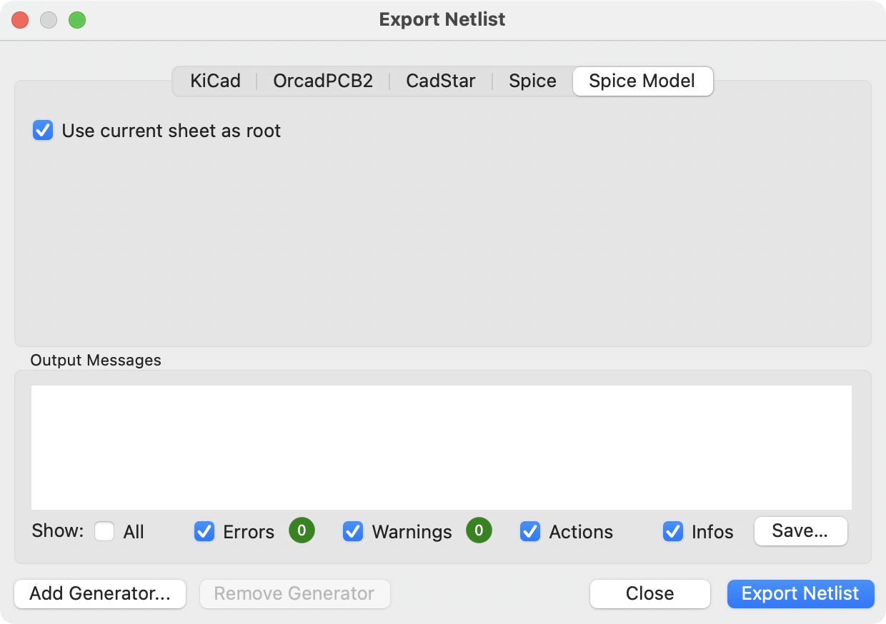
KiCad can also export a netlist of the schematic as a Spice subcircuit model, which can be included in a separate Spice simulation. Any hierarchical labels in the schematic are used as pins for the subcircuit model. Each pin in the model is annotated with a comment describing the pin’s electrical direction:
-
Inputhierarchical labels are mapped to aninputannotation -
Outputhierarchical labels are mapped to anoutputannotation -
Bidirectionalhierarchical labels are mapped to aninoutannotation -
Tri-statehierarchical labels are mapped to atristateannotation -
Passivehierarchical labels are mapped to apassiveannotation
When the use current sheet as root is selected, only the current sheet is exported to a subcircuit model. Otherwise, the entire schematic sheet is exported.
Netlist examples
Below is the schematic from the sallen_key project included in KiCad’s
simulation demos.
The KiCad format netlist for this schematic is as follows:
(export (version "E")
  (design
    (source "/usr/share/kicad/demos/simulation/sallen_key/sallen_key.kicad_sch")
    (date "Sun 01 May 2022 03:14:05 PM EDT")
    (tool "Eeschema (6.0.4)")
    (sheet (number "1") (name "/") (tstamps "/")
      (title_block
        (title)
        (company)
        (rev)
        (date)
        (source "sallen_key.kicad_sch")
        (comment (number "1") (value ""))
        (comment (number "2") (value ""))
        (comment (number "3") (value ""))
        (comment (number "4") (value ""))
        (comment (number "5") (value ""))
        (comment (number "6") (value ""))
        (comment (number "7") (value ""))
        (comment (number "8") (value ""))
        (comment (number "9") (value "")))))
  (components
    (comp (ref "C1")
      (value "100n")
      (libsource (lib "sallen_key_schlib") (part "C") (description ""))
      (property (name "Sheetname") (value ""))
      (property (name "Sheetfile") (value "sallen_key.kicad_sch"))
      (sheetpath (names "/") (tstamps "/"))
      (tstamps "00000000-0000-0000-0000-00005789077d"))
    (comp (ref "C2")
      (value "100n")
      (fields
        (field (name "Fieldname") "Value")
        (field (name "SpiceMapping") "1 2")
        (field (name "Spice_Primitive") "C"))
      (libsource (lib "sallen_key_schlib") (part "C") (description ""))
      (property (name "Fieldname") (value "Value"))
      (property (name "Spice_Primitive") (value "C"))
      (property (name "SpiceMapping") (value "1 2"))
      (property (name "Sheetname") (value ""))
      (property (name "Sheetfile") (value "sallen_key.kicad_sch"))
      (sheetpath (names "/") (tstamps "/"))
      (tstamps "00000000-0000-0000-0000-00005789085b"))
    (comp (ref "R1")
      (value "1k")
      (fields
        (field (name "Fieldname") "Value")
        (field (name "SpiceMapping") "1 2")
        (field (name "Spice_Primitive") "R"))
      (libsource (lib "sallen_key_schlib") (part "R") (description ""))
      (property (name "Fieldname") (value "Value"))
      (property (name "SpiceMapping") (value "1 2"))
      (property (name "Spice_Primitive") (value "R"))
      (property (name "Sheetname") (value ""))
      (property (name "Sheetfile") (value "sallen_key.kicad_sch"))
      (sheetpath (names "/") (tstamps "/"))
      (tstamps "00000000-0000-0000-0000-0000578906ff"))
    (comp (ref "R2")
      (value "1k")
      (fields
        (field (name "Fieldname") "Value")
        (field (name "SpiceMapping") "1 2")
        (field (name "Spice_Primitive") "R"))
      (libsource (lib "sallen_key_schlib") (part "R") (description ""))
      (property (name "Fieldname") (value "Value"))
      (property (name "SpiceMapping") (value "1 2"))
      (property (name "Spice_Primitive") (value "R"))
      (property (name "Sheetname") (value ""))
      (property (name "Sheetfile") (value "sallen_key.kicad_sch"))
      (sheetpath (names "/") (tstamps "/"))
      (tstamps "00000000-0000-0000-0000-000057890691"))
    (comp (ref "U1")
      (value "AD8051")
      (fields
        (field (name "Spice_Lib_File") "ad8051.lib")
        (field (name "Spice_Model") "AD8051")
        (field (name "Spice_Netlist_Enabled") "Y")
        (field (name "Spice_Primitive") "X"))
      (libsource (lib "sallen_key_schlib") (part "Generic_Opamp") (description ""))
      (property (name "Spice_Primitive") (value "X"))
      (property (name "Spice_Model") (value "AD8051"))
      (property (name "Spice_Lib_File") (value "ad8051.lib"))
      (property (name "Spice_Netlist_Enabled") (value "Y"))
      (property (name "Sheetname") (value ""))
      (property (name "Sheetfile") (value "sallen_key.kicad_sch"))
      (sheetpath (names "/") (tstamps "/"))
      (tstamps "00000000-0000-0000-0000-00005788ff9f"))
    (comp (ref "V1")
      (value "AC 1")
      (libsource (lib "sallen_key_schlib") (part "VSOURCE") (description ""))
      (property (name "Sheetname") (value ""))
      (property (name "Sheetfile") (value "sallen_key.kicad_sch"))
      (sheetpath (names "/") (tstamps "/"))
      (tstamps "00000000-0000-0000-0000-000057336052"))
    (comp (ref "V2")
      (value "DC 10")
      (fields
        (field (name "Fieldname") "Value")
        (field (name "Spice_Node_Sequence") "1 2")
        (field (name "Spice_Primitive") "V"))
      (libsource (lib "sallen_key_schlib") (part "VSOURCE") (description ""))
      (property (name "Fieldname") (value "Value"))
      (property (name "Spice_Primitive") (value "V"))
      (property (name "Spice_Node_Sequence") (value "1 2"))
      (property (name "Sheetname") (value ""))
      (property (name "Sheetfile") (value "sallen_key.kicad_sch"))
      (sheetpath (names "/") (tstamps "/"))
      (tstamps "00000000-0000-0000-0000-0000578900ba"))
    (comp (ref "V3")
      (value "DC 10")
      (fields
        (field (name "Fieldname") "Value")
        (field (name "Spice_Node_Sequence") "1 2")
        (field (name "Spice_Primitive") "V"))
      (libsource (lib "sallen_key_schlib") (part "VSOURCE") (description ""))
      (property (name "Fieldname") (value "Value"))
      (property (name "Spice_Primitive") (value "V"))
      (property (name "Spice_Node_Sequence") (value "1 2"))
      (property (name "Sheetname") (value ""))
      (property (name "Sheetfile") (value "sallen_key.kicad_sch"))
      (sheetpath (names "/") (tstamps "/"))
      (tstamps "00000000-0000-0000-0000-000057890232")))
  (libparts
    (libpart (lib "sallen_key_schlib") (part "C")
      (footprints
        (fp "C?")
        (fp "C_????_*")
        (fp "C_????")
        (fp "SMD*_c")
        (fp "Capacitor*"))
      (fields
        (field (name "Reference") "C")
        (field (name "Value") "C"))
      (pins
        (pin (num "1") (name "") (type "passive"))
        (pin (num "2") (name "") (type "passive"))))
    (libpart (lib "sallen_key_schlib") (part "Generic_Opamp")
      (fields
        (field (name "Reference") "U")
        (field (name "Value") "Generic_Opamp"))
      (pins
        (pin (num "1") (name "+") (type "input"))
        (pin (num "2") (name "-") (type "input"))
        (pin (num "3") (name "V+") (type "power_in"))
        (pin (num "4") (name "V-") (type "power_in"))
        (pin (num "5") (name "") (type "output"))))
    (libpart (lib "sallen_key_schlib") (part "R")
      (footprints
        (fp "R_*")
        (fp "Resistor_*"))
      (fields
        (field (name "Reference") "R")
        (field (name "Value") "R"))
      (pins
        (pin (num "1") (name "") (type "passive"))
        (pin (num "2") (name "") (type "passive"))))
    (libpart (lib "sallen_key_schlib") (part "VSOURCE")
      (fields
        (field (name "Reference") "V")
        (field (name "Value") "VSOURCE")
        (field (name "Fieldname") "Value")
        (field (name "Spice_Primitive") "V")
        (field (name "Spice_Node_Sequence") "1 2"))
      (pins
        (pin (num "1") (name "") (type "input"))
        (pin (num "2") (name "") (type "input")))))
  (libraries
    (library (logical "sallen_key_schlib")
      (uri "/usr/share/kicad/demos/simulation/sallen_key/sallen_key_schlib.kicad_sym")))
  (nets
    (net (code "1") (name "/lowpass")
      (node (ref "C1") (pin "1") (pintype "passive"))
      (node (ref "U1") (pin "2") (pinfunction "-") (pintype "input"))
      (node (ref "U1") (pin "5") (pintype "output")))
    (net (code "2") (name "GND")
      (node (ref "C2") (pin "2") (pintype "passive"))
      (node (ref "V1") (pin "2") (pintype "input"))
      (node (ref "V2") (pin "2") (pintype "input"))
      (node (ref "V3") (pin "1") (pintype "input")))
    (net (code "3") (name "Net-(C1-Pad2)")
      (node (ref "C1") (pin "2") (pintype "passive"))
      (node (ref "R1") (pin "1") (pintype "passive"))
      (node (ref "R2") (pin "2") (pintype "passive")))
    (net (code "4") (name "Net-(C2-Pad1)")
      (node (ref "C2") (pin "1") (pintype "passive"))
      (node (ref "R2") (pin "1") (pintype "passive"))
      (node (ref "U1") (pin "1") (pinfunction "+") (pintype "input")))
    (net (code "5") (name "Net-(R1-Pad2)")
      (node (ref "R1") (pin "2") (pintype "passive"))
      (node (ref "V1") (pin "1") (pintype "input")))
    (net (code "6") (name "VDD")
      (node (ref "U1") (pin "3") (pinfunction "V+") (pintype "power_in"))
      (node (ref "V2") (pin "1") (pintype "input")))
    (net (code "7") (name "VSS")
      (node (ref "U1") (pin "4") (pinfunction "V-") (pintype "power_in"))
      (node (ref "V3") (pin "2") (pintype "input")))))
In Spice format, the netlist is as follows:
.title KiCad schematic
.include "ad8051.lib"
XU1 Net-_C2-Pad1_ /lowpass VDD VSS /lowpass AD8051
C2 Net-_C2-Pad1_ GND 100n
C1 /lowpass Net-_C1-Pad2_ 100n
R2 Net-_C2-Pad1_ Net-_C1-Pad2_ 1k
R1 Net-_C1-Pad2_ Net-_R1-Pad2_ 1k
V1 Net-_R1-Pad2_ GND AC 1
V2 VDD GND DC 10
V3 GND VSS DC 10
.ac dec 10 1 1Meg
.end
Symbols and Symbol Libraries
KiCad organizes symbols into symbol libraries, which hold collections of
symbols. Each symbol in a schematic is uniquely identified by a full name that
is composed of a library nickname and a symbol name. For example, the identifier
Audio:AD1853 refers to the AD1853 symbol in the Audio library.
Managing symbol libraries
KiCad uses a table of symbol libraries to map a symbol library nickname to an underlying symbol library on disk. Kicad uses a global symbol library table as well as a table specific to each project. To edit either symbol library table, use Preferences → Manage Symbol Libraries….
The global symbol library table contains the list of libraries that are
always available regardless of the currently loaded project. The table is
saved in the file sym-lib-table in the KiCad configuration folder.
The location of this folder
depends on the operating system being used.
The project specific symbol library table contains the list of libraries that
are available specifically for the currently loaded project. If there are any
project-specific symbol libraries, the table is saved in the file
sym-lib-table in the project folder.
Initial Configuration
The first time the KiCad Schematic Editor is run and the global symbol table
file sym-lib-table is not found in the KiCad configuration folder, KiCad will
guide the user through setting up a new symbol library table. This process is
described above.
Managing Table Entries
Symbol libraries can only be used if they have been added to either the global or project-specific symbol library table.
Add a library either by clicking the
![]() button and selecting a
library or clicking the
button and selecting a
library or clicking the ![]() button
and typing the path to a library file. The selected library will be added to the
currently opened library table (Global or Project Specific). Libraries can be
removed by selecting desired library entries and clicking the
button
and typing the path to a library file. The selected library will be added to the
currently opened library table (Global or Project Specific). Libraries can be
removed by selecting desired library entries and clicking the
![]() button.
button.
The ![]() and
and
![]() buttons move the selected
library up and down in the library table. This does not affect the display order
of libraries in the Symbol Library Browser, Symbol Editor, or Add Symbol tool.
buttons move the selected
library up and down in the library table. This does not affect the display order
of libraries in the Symbol Library Browser, Symbol Editor, or Add Symbol tool.
Libraries can be made inactive by unchecking the Active checkbox in the first column. Inactive libraries are still in the library table but do not appear in any library browsers and are not loaded from disk, which can reduce loading times.
A range of libraries can be selected by clicking the first library in the range and then Shift-clicking the last library in the range.
Each library must have a unique nickname: duplicate library nicknames are not allowed in the same table. However, nicknames can be duplicated between the global and project library tables. Libraries in the project table take precedence over libraries with the same name in the global table.
Library nicknames do not have to be related to the library filename or path. The
colon character (:) cannot be used in library nicknames or symbol names
because it is used as a separator between nicknames and symbols.
Each library entry must have a valid path. Paths can be defined as absolute, relative, or by environment variable substitution.
The appropriate library format must be selected in order for the library
to be properly read. "KiCad" format is used for KiCad version 6+ libraries
(.kicad_sym files), while "Legacy" format is used for libraries from
older versions of KiCad (.lib files). Legacy libraries are read-only,
but can be migrated to KiCad format libraries using the Migrate
Libraries button (see section Migrating Legacy Libraries).
There is an optional description field to add a description of the library entry. The option field is not used at this time so adding options will have no effect when loading libraries.
Environment Variable Substitution
The symbol library tables support environment variable substitution, which
allows you to define environment variables containing custom paths to where your
libraries are stored. Environment variable substitution is supported by using
the syntax ${ENV_VAR_NAME} in the symbol library path.
By default, KiCad defines several environment variables which are described in the project manager documentation. Environment variables can be configured in the Preferences → Configure Paths… dialog.
Using environment variables in the symbol library tables allows libraries to be relocated without breaking the symbol library tables, so long as the environment variables are updated when the library location changes.
${KIPRJMOD} is a special environment variable that always expands to the
absolute path of the current project directory. ${KIPRJMOD} allows libraries
to be stored in the project folder without having to use an absolute path in the
project library table. This makes it possible to relocate projects without
breaking their project library tables.
Usage Patterns
Symbol libraries can be defined either globally or specifically to the currently
loaded project. Symbol libraries defined in the user’s global table are always
available and are stored in the sym-lib-table file in the user’s KiCad
configuration folder. The project-specific symbol library table is active only
for the currently open project file.
There are advantages and disadvantages to each method. Defining all libraries in the global table means they will always be available when needed. The disadvantage of this is that load time will increase.
Defining all symbol libraries on a project specific basis means that you only have the libraries required for the project which decreases symbol library load times. The disadvantage is that you always have to remember to add each symbol library that you need for every project.
One usage pattern would be to define commonly used libraries globally and the libraries only required for the project in the project specific library table. There is no restriction on how to define libraries.
Migrating Legacy Libraries
Legacy libraries (.lib files) are read-only, but they can be migrated
to KiCad version 6 libraries (.kicad_sym). KiCad version 6 libraries
cannot be viewed or edited by KiCad versions older than 6.0.0.
Legacy libraries can be converted to KiCad 6 libraries by selecting them in the symbol library table and clicking the Migrate Libraries button. Multiple libraries can be selected and migrated at once by Ctrl-clicking or shift-clicking.
Libraries can also be converted one at a time by opening them in the Symbol Editor and saving them as a new library.
Legacy Project Remapping
When loading a schematic created prior to the symbol library table implementation, KiCad will attempt to remap the symbol library links in the schematic to the appropriate library table symbols. The success of this process is dependent on several factors:
-
the original libraries used in the schematic are still available and unchanged from when the symbol was added to the schematic.
-
all rescue operations were performed when detected to create a rescue library or keep the existing rescue library up to date.
-
the integrity of the project symbol cache library has not been corrupted.
|
The remapping will make a back up of all the files that are changed during remapping in the rescue-backup folder in the project folder. Always make a back up of your project before remapping just in case something goes wrong. |
|
The rescue operation is performed even if it has been disabled to ensure the correct symbols are available for remapping. Do not cancel this operation or the remapping will fail to correctly remap schematics symbols. Any broken symbol links will have to be fixed manually. |
|
If the original libraries have been removed and the rescue was not performed, the cache library can be used as a recovery library as a last resort. Copy the cache library to a new file name and add the new library file to the top of the library list using a version of KiCad prior to the symbol library table implementation. |
Creating and editing symbols
Overview of symbols and symbol libraries
A symbol is a schematic representation of a component. A symbol is composed of:
-
Graphical items (lines, circles, arcs, text, etc.) that determine how symbol looks in a schematic.
-
Pins, which have both graphic properties (line, clock, inverted, low level active, etc.) and electrical properties (input, output, bidirectional, etc.) used by the Electrical Rules Check (ERC) tool.
-
Fields, such as references, values, corresponding footprint names for PCB design, etc.
A symbol library is composed of one or more symbols. Generally the symbols are logically grouped by function, type, and/or manufacturer.
Symbols can be derived from another symbol in the same library. Derived symbols share the base symbol’s graphical shape and pin definitions, but can override the base symbol’s property fields (value, footprint, footprint filters, datasheet, description, etc.). Derived symbols can be used to define symbols that are similar to a base part. For example, 74LS00, 74HC00, and 7437 symbols could all be derived from a 7400 symbol. In previous versions of KiCad, derived symbols were referred to as aliases.
Symbol Editor overview
KiCad provides a symbol editing tool that allows you to create libraries, add, delete or transfer symbols between libraries, export symbols to files, and import symbols from files.
In general, the flow for designing a symbol involves:
-
Defining if the symbol is made up of one or more units.
-
Defining if the symbol has an alternate body style (also known as a De Morgan representation).
-
Designing its symbolic representation using lines, rectangles, circles, polygons and text.
-
Adding pins by carefully defining each pin’s graphical elements, name, number, and electrical property (input, output, tri-state, power output, etc.).
-
Determining if the symbol should be derived from another symbol with the same graphical design and pin definition.
-
Adding optional fields such as the name of the footprint used by the PCB design software and/or defining their visibility.
-
Documenting the symbol by adding a description string and links to data sheets, etc.
-
Saving it in the desired library.
The Symbol Editor main window is shown below. It consists of three toolbars for quick access to common features and a symbol viewing/editing area. Not all commands are available on the toolbars, but all commands are available in the menus.
Main Toolbar
The main toolbar is at the top of the main window. It has buttons for the undo/redo commands, zoom commands, symbol properties dialogs, and unit/representation management controls.
|
Create a new symbol in the selected library. |
|
Save the currently selected library. All modified symbols in the library will be saved. |
|
Undo last edit. |
|
Redo last undo. |
|
Refresh display. |
|
Zoom in. |
|
Zoom out. |
|
Zoom to fit symbol in display. |
|
Zoom to fit selection. |
|
Rotate counter-clockwise. |
|
Rotate clockwise. |
|
Mirror horizontally. |
|
Mirror vertically. |
|
Edit the current symbol properties. |
|
Edit the symbol’s pins in a tabular interface. |
|
Open the symbol’s datasheet, if it is defined. |
|
Test the current symbol for design errors. |
|
Select the normal body style. The button is disabled if the current symbol does not have an alternate body style. |
|
Select the alternate body style. The button is disabled if the current symbol does not have an alternate body style. |
|
Select the unit of a multi-unit symbol to display. The drop down control will be disabled if the current symbol is not derived from a symbol with multiple units. |
|
Enable synchronized pins edit mode. When this mode is enabled, any pin modifications are propagated to all other symbol units. Pin number changes are not propagated. This mode is automatically enabled for symbols with multiple interchangeable units and cannot be enabled for symbols with only one unit. |
|
Insert current symbol into the schematic. |
Element Toolbar
The vertical toolbar located on the right hand side of the main window allows you to place all of the elements required to design a symbol.
|
Select tool. Right-clicking with the select tool opens the context menu for the object under the cursor. Left-clicking with the select tool displays the attributes of the object under the cursor in the message panel at the bottom of the main window. Double-left-clicking with the select tool will open the properties dialog for the object under the cursor. |
|
Pin tool. Left-click to add a new pin. |
|
Graphical text tool. Left-click to add a new graphical text item. |
|
Graphical textbox tool. Left-click to add a new graphical textbox item. |
|
Rectangle tool. Left-click to begin drawing the first corner of a graphical rectangle. Left-click again to place the opposite corner of the rectangle. |
|
Circle tool. Left-click to begin drawing a new graphical circle from the center. Left-click again to define the radius of the circle. |
|
Arc tool. Left-click to begin drawing a new graphical arc item from the first arc end point. Left-click again to define the second arc end point. Adjust the radius by dragging the arc center point. |
|
Connected line tool. Left-click to begin drawing a new graphical line item in the current symbol. Left-click for each additional connected line. Double-left-click to complete the line. |
|
Anchor tool. Left-click to set the anchor position of the symbol. |
|
Delete tool. Left-click to delete an object from the current symbol. |
Options Toolbar
The vertical tool bar located on the left hand side of the main window allows you to set some of the editor drawing options.
|
Toggle grid visibility on and off. |
|
Set units to inches. |
|
Set units to mils (0.001 inch). |
|
Set units to millimeters. |
|
Toggle full screen cursor on and off. |
|
Toggle display of pin electrical types. |
|
Toggle display of library and symbol tree. |
Saving symbols to libraries
The ![]() button displays or
hides the list of available libraries, which allows you to select an active
library. When a symbol is saved, it will be placed in this library.
button displays or
hides the list of available libraries, which allows you to select an active
library. When a symbol is saved, it will be placed in this library.
Clicking the ![]() icon
on the left toolbar toggles the treeview of libraries and symbols. Clicking on
a symbol opens that symbol.
icon
on the left toolbar toggles the treeview of libraries and symbols. Clicking on
a symbol opens that symbol.
| Some symbols are derived from other symbols. Derived symbol names are displayed in italics in the treeview. If a derived symbol is opened, its symbol graphics will not be editable. Its symbol fields will be editable as normal. To edit the graphics of a base symbol and all of its derived symbols, open the base symbol. |
After modification, a symbol can be saved in the current library or a different library.
To save the modified symbol in the current library, click the
![]() icon. The modifications will be
written to the existing symbol.
icon. The modifications will be
written to the existing symbol.
| Saving a modified symbol also saves all other modified symbols in the same library. |
To save the symbol changes to a new symbol, click File → Save As…. The symbol can be saved in the current library or a different library. A new name can be set for the symbol.
To create a new file containing only the current symbol, click File → Export → Symbol…. This file will be a standard library file which will contain only one symbol.
Creating symbols
Creating a new symbol
A new symbol can be created by clicking the
![]() icon.
You will be asked for a number of symbol properties.
icon.
You will be asked for a number of symbol properties.
-
A symbol name
-
An optional base symbol to derive the new symbol from. The new symbol will use the base symbol’s graphical shape and pin configuration, but other symbol information can be modified in the derived symbol. The base symbol must be in the same library as the new derived symbol.
-
The reference designator prefix (
U,C,R…). -
The number of units per package, and whether those units are interchangeable (for example a 7400 quad NAND symbol could have 4 units, one for each gate).
-
If an alternate body style (sometimes referred to as a "De Morgan equivalent") is desired.
-
Whether the symbol is a power symbol. Power symbols appear in the Add Power Symbol dialog in the Schematic editor, their
Valuefields are not editable in the schematic, they cannot be assigned a footprint, they are not added to the PCB, and they are not included in the bill of materials. -
Whether the symbol should be excluded from the bill of materials.
-
Whether the symbol should be excluded from the PCB.
There are also several graphical options.
-
The offset between the end of each pin and its pin name.
-
Whether the pin number and pin name should be displayed.
-
Whether the pin names should be displayed alongside the pins or at the ends of the pins inside the symbol body.
These properties can also be changed later in the Symbol Properties window.
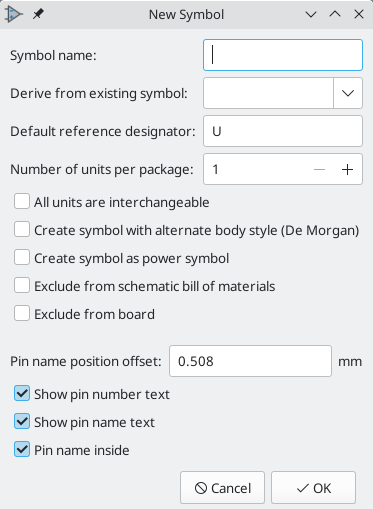
A new symbol will be created using the properties above and will appear in the editor as shown below.
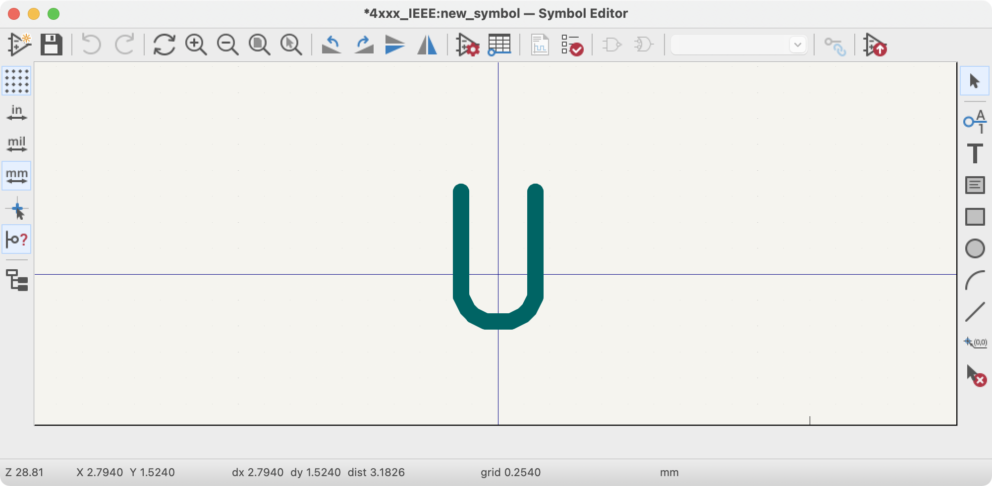
The blue cross in the center is the symbol anchor, which specifies the symbol
origin i.e. the coordinates (0, 0). The anchor can be repositioned by selecting
the ![]() icon and clicking on the new
desired anchor position.
icon and clicking on the new
desired anchor position.
Creating a symbol from another symbol
Often, the symbol that you want to make is similar to one already in a symbol library. In this case it is easy to load and modify an existing symbol.
-
Load the symbol which will be used as a starting point.
-
Save a new copy of the symbol using File → Save As…. The Save As dialog will prompt for a name for the new symbol and the library to save it in.
-
Edit the new symbol as required.
-
Save the modified symbol.
Symbol Properties
Symbol properties are set when the symbol is created but they can be modified
at any point. To change the symbol properties, click on the
![]() button
to show the Symbol Properties dialog. You can also double click an empty spot in
the editing canvas.
button
to show the Symbol Properties dialog. You can also double click an empty spot in
the editing canvas.
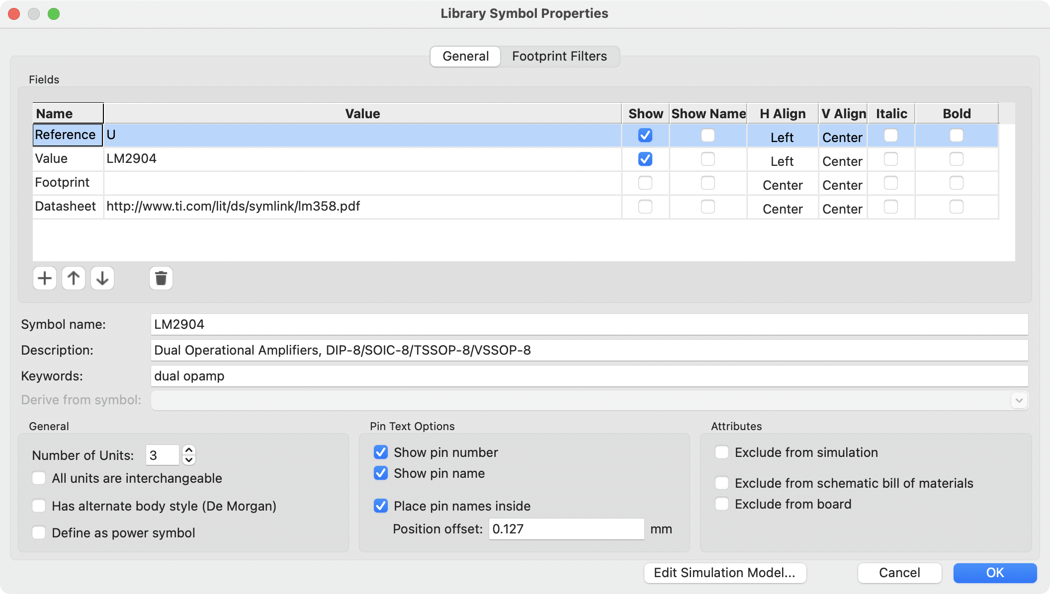
It is important to set the number of units and check all units are interchangeable and has alternate body style, as applicable, because these settings affect how pins and graphics are added to each symbol unit.
If you change the number of units per package after adding the pins to the symbol, you will need to do extra work to add pins and graphics for the additional units. The pins and graphics would have been automatically added to each unit had these properties been correctly set initially. Nevertheless, it is possible to modify these properties at any time.
The graphic options Show pin number and Show pin name define the
visibility of the pin number and pin name text. The option Place pin
names inside defines the pin name position relative to the pin body.
The pin names will be displayed inside the symbol outline if the option
is checked. In this case the Pin Name Position Offset property defines
the shift of the text away from the body end of the pin. A value from
0.02 to 0.05 inches is usually reasonable.
The example below shows a symbol with the Place pin name inside option unchecked. Notice the position of the names and pin numbers.
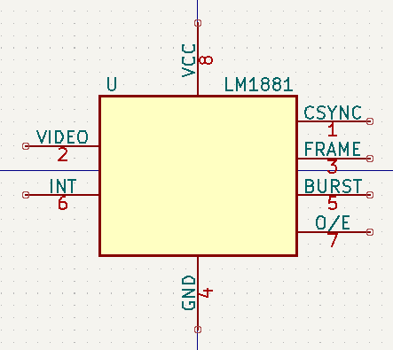
Symbol Name, Description, and Keywords
Symbol name is the symbol’s name in the library. Symbols are identified by a combination of the library and symbol name.
In previous versions of KiCad, the symbol name was linked to the Value field.
This link is removed in KiCad 7.0 and later.
The symbol description should contain a brief description of the component, such as the component function, distinguishing features, and package options. The keywords should contain additional terms related to the component. Keywords are used primarily to assist in searching for the symbol.
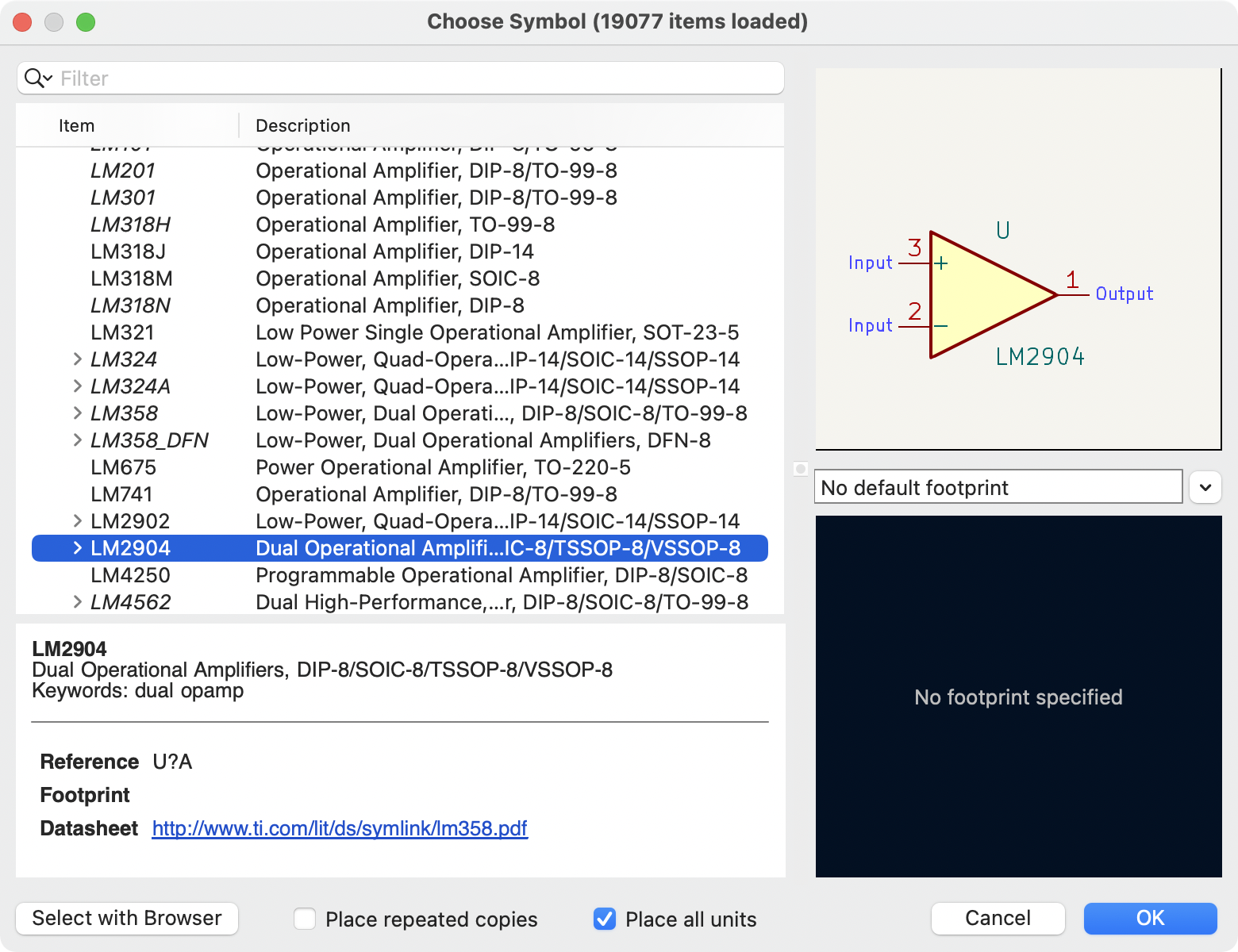
A symbol’s name, description, and keywords are all used when searching for symbols in the Symbol Editor and Add a Symbol dialog. The description and keywords are displayed in the Symbol Library Browser and Add a Symbol dialog.
Footprint Filters
The footprint filters tab is used to define which footprints are appropriate to use with the symbol. The filters can be applied in the Footprint Assignment tool so that only appropriate footprints are displayed for each symbol.
Multiple footprint filters can be defined. Footprints that match any of the filters will be displayed; if no filters are defined, then all footprints will be displayed.
Filters can use wildcards: * matches any number of characters,
including zero, and ? matches zero or one characters. For example, SOIC-*
would match the SOIC-8_3.9x4.9mm_P1.27mm footprint as well as any other
footprint beginning with SOIC-. The filter SOT?23 matches SOT23 as well as
SOT-23.
Symbols with Alternate Symbolic Representation
If the symbol has an alternate body style defined, one body style must be
selected for editing at a time. To edit the normal representation, click
the ![]() icon.
icon.
To edit the alternate representation, click on the
![]() icon.
Use the
icon.
Use the
 unit selection dropdown to select the unit you wish to edit.
Graphical Elements
Graphical elements create the visual representation of a symbol and contain no electrical connection information. Graphical elements are created with the following tools:
-
Lines and polygons defined by start and end points.
-
Rectangles defined by two diagonal corners.
-
Circles defined by the center and radius.
-
Arcs defined by the starting and ending point of the arc and its center. An arc goes from 0° to 180°.
The vertical toolbar on the right hand side of the main window allows you to place all of the graphical elements required to design the representation of a symbol.
Graphical Element Membership
Each graphic element (line, arc, circle, etc.) can be defined as common to all units and/or body styles or specific to a given unit and/or body style. Element options can be quickly accessed by right-clicking on the element to display the context menu for the selected element. Below is the context menu for a line element.
You can also double-left-click on an element to modify its properties. Below is the properties dialog for a polygon element.
The properties of a graphic element are:
-
Border determines whether the the shape’s outline should be drawn.
-
Width and color define the line width and color of the border. A border width of
0uses the schematic’s default symbol line width. Style determines the line style of the border (solid, dashed, dotted, etc.). -
Fill Style determines if the shape defined by the graphical element is to be drawn unfilled or filled. The fill color can be the color theme’s body outline color, body background color, or a custom color.
-
Common to all units in symbol determines if the graphical element is drawn for each unit in symbol with more than one unit per package or if the graphical element is only drawn for the current unit.
-
Common to all body styles (De Morgan) determines if the graphical element is drawn for each symbolic representation in symbols with an alternate body style or if the graphical element is only drawn for the current body style.
-
Private to Symbol Editor causes the shape to be visible only when the symbol is edited in the Symbol Editor. The shape will be hidden when the symbol is added to a schematic.
Graphical Text Elements
The ![]() icon
allows for the creation of graphical text. Graphical text is automatically
oriented to be readable, even when the symbol is mirrored. Please note that
graphical text items are not the same as symbol fields.
icon
allows for the creation of graphical text. Graphical text is automatically
oriented to be readable, even when the symbol is mirrored. Please note that
graphical text items are not the same as symbol fields.
Multiple Units per Symbol and Alternate Body Styles
Symbols can have up to two body styles (a standard symbol and an alternate symbol often referred to as a "De Morgan equivalent") and/or have more than one unit per package (logic gates for example). Some symbols can have more than one unit per package each with different symbols and pin configurations.
For example, consider a relay with two switches, which can be designed as a symbol with three different units: a coil, switch 1, and switch 2. Designing a symbol with multiple units per package and/or alternate body styles is very flexible. A pin or a body symbol item can be common to all units or specific to a given unit or they can be common to both symbolic representation so are specific to a given symbol representation.
By default, pins are specific to a unit and body style. When a pin is common to all units or all body styles, it only needs to be created once. This is also the case for the body style graphic shapes and text, which may be common to each unit, but typically are specific to each body style.
To add additional units to a symbol, set the Number of Units property to the
appropriate number in the Symbol Properties dialog. By default, symbol units are
named Unit A, Unit B, etc., but you can set an arbitrary name for the
current unit using Edit → Set Unit Display Name….
To add an alternate body style, set the Has alternate body style (De Morgan) property in the Symbol Properties dialog.
Example of a Symbol With Multiple Noninterchangeable Units
For an example of a symbol with multiple units that are not interchangeable, consider a relay with 3 units per package: a coil, switch 1, and switch 2.
The three units are not all the same, so All units are interchangeable should be deselected in the Symbol Properties dialog. Alternatively, this option could have been specified when the symbol was initially created.
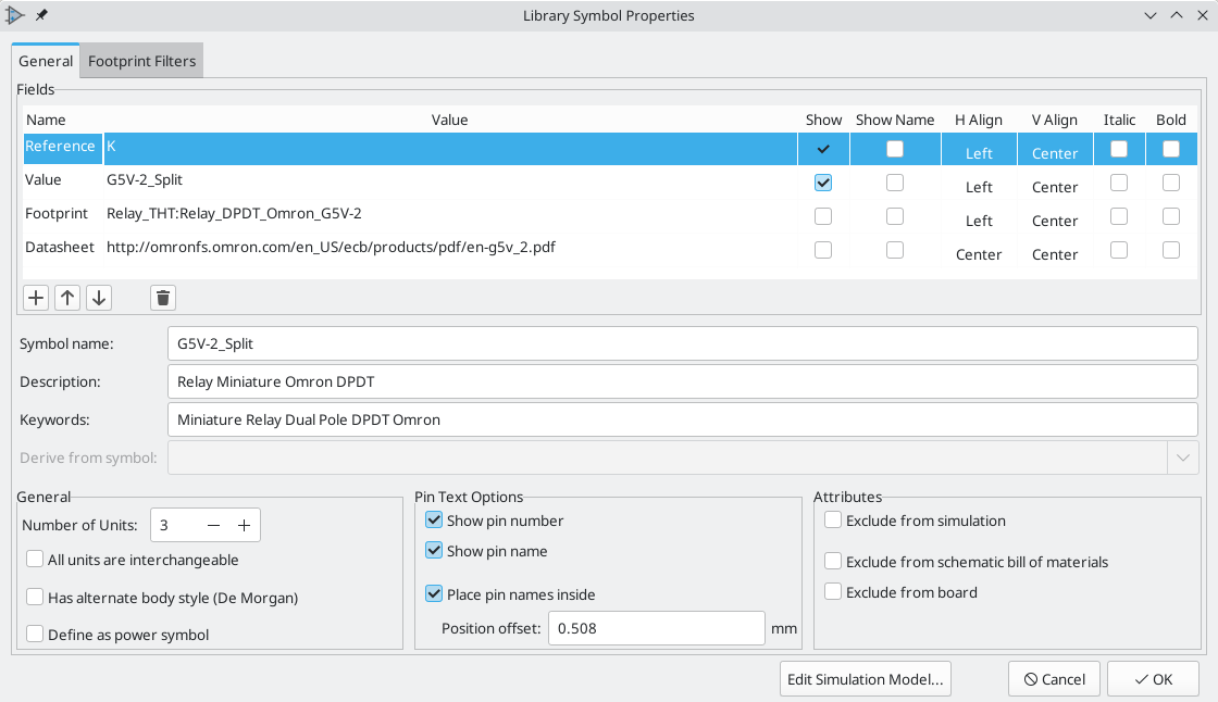
Unit A
Unit B
Unit C
Unit A does not have the same symbol and pin layout as Units B and C, so the units are not interchangeable.
|
Synchronized Pins Edit Mode can be enabled by clicking the
|
Pin Creation and Editing
You can create and insert a pin by clicking on the
![]() button. Pin properties can be edited by
double clicking on the pin. You can also delete or move pins that you have
already added. Pins must be created carefully, because any error will have
consequences on the PCB design.
button. Pin properties can be edited by
double clicking on the pin. You can also delete or move pins that you have
already added. Pins must be created carefully, because any error will have
consequences on the PCB design.
Pin Overview
A pin is defined by its graphical representation, its name, and its number. The pin’s name and number can contain letters, numbers, and symbols, but not spaces. For the Electrical Rules Check (ERC) tool to be useful, the pin’s electrical type (input, output, tri-state…) must also be defined correctly. If this type is not defined properly, the schematic ERC check results may be invalid.
Important notes:
-
Symbol pins are matched to footprint pads by number. The pin number in the symbol must match the corresponding pad number in the footprint.
-
Do not use spaces in pin names and numbers. Spaces will be automatically replaced with underscores (
_). -
To define a pin name with an inverted signal (overbar) use the
~(tilde) character followed by the text to invert in braces. For example~{FO}Owould display FO O. -
If the pin name is empty, the pin is considered unnamed.
-
Pin names can be repeated in a symbol.
-
Pin numbers must be unique in a symbol.
Pin Properties
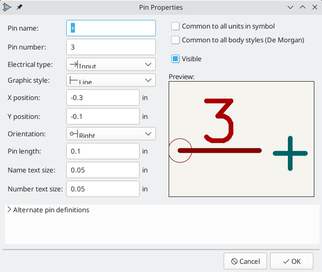
The pin properties dialog allows you to edit all of the characteristics of a pin. This dialog pops up automatically when you create a pin or when double-clicking on an existing pin. This dialog allows you to modify:
-
The pin name and text size.
-
The pin number and text size.
-
The pin length.
-
The pin electrical type and graphical style.
-
Unit and alternate representation membership.
-
Pin visibility.
Pin Graphic Styles
The different pin graphic styles are shown in the figure below. These styles are purely graphical and do not affect the pin’s electrical type.
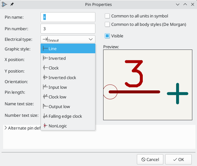
Pin Electrical Types
Each pin in a symbol has an electrical type, such as input, output, or tri-state.
Choosing the correct electrical type is important for the schematic ERC tool. ERC will check that pins are connected appropriately, for example ensuring that input pins are driven and power inputs receive power from an appropriate source.
You can use the Pin Conflicts Map in the schematic editor to configure which pin types are allowed to connect and which will conflict. The default Pin Conflicts settings are briefly explained below. For more information, see the ERC documentation.
Additionally, some pin types have special behavior outside of ERC: in the router, pads corresponding to a free pin can be connected to copper of any other net without causing a DRC error, and pads corresponding to stacked unconnected pins do not need to be connected to each other.
Pin Type |
Description |
Input |
A pin which is exclusively an input. The default Pin Conflicts settings allow input pins to connect to most other types of pin. |
Output |
A pin which is exclusively an output. The default Pin Conflicts settings allow output pins to connect to most types of pin that aren’t also outputs. |
Bidirectional |
A pin that can be either an input or an output, such as a microcontroller data bus pin. The default Pin Conflicts settings allow bidirectional pins to connect to most other types of pins, though there are a few more restrictions than with input pins. |
Tri-state |
A three state output pin (high, low, or high impedance). The default Pin Conflicts settings allow tri-state pins to connect to most other types of pins, but warnings are generated when they are connected to most types of output or power pins. |
Passive |
A pin that is not connected to active electronics, for example pins on a resistor or connector. The default Pin Conflicts settings allow passive pins to connect to most other types of pin. |
Free |
A pin that does not electrically affect the operation of the device. These pins typically represent package leads that are not internally connected to the chip. The default Pin Conflicts settings allow free pins to connect to most other types of pin. In the PCB editor, pads corresponding to free pins can be connected to copper of any other net without causing a DRC error. |
Unspecified |
A pin which has an unspecified type. With the default Pin Conflicts settings, ERC generates warnings when unspecified pins are connected to most other types of pins. |
Power input |
A pin that powers the device. The default Pin Conflicts settings allow power input pins to connect to most other pin types. However, power input pins that are not connected to a power output pin generate an ERC violation. Additionally, power input pins that are marked invisible are automatically connected to the net with the same name as the pin. See the Power Symbols section for more information. |
Power output |
A pin that provides power to other pins, such as a regulator output. The default Pin Conflicts settings allow power output pins to connect to most types of output pins, but not input pins. |
Open collector |
An open collector logic output. The default Pin Conflicts settings allow open collector pins to connect to most input pins and other open collector pins, but not to most other types of outputs. |
Open emitter |
An open emitter logic output. The default Pin Conflicts settings allow open collector pins to connect to most input pins and other open emitter pins, but not to most other types of outputs. |
Unconnected |
A pin that should not be connected to anything. The default Pin Conflict settings do not allow pins of type unconnected to connect to any other type of pin, and ERC will not generate an "unconnected pin" violation when pins of this type are left unconnected. If a footprint has multiple pads corresponding to a single unconnected pin, the pads do not need to be connected to each other in the board. When multiple pins of type unconnected are stacked in a symbol, they are connected to separate nets, whereas stacked pins of other types are connected to the same net. Note that this pin type is different than placing a no connect flag on a pin in the schematic. The unconnected pin type indicates that the pin should never be connected in any schematic, while a no connect flag indicates that the pin is intentionally unconnected in the current schematic. |
Pushing Pin Properties to Other Pins
You can apply the length, name size, or number size of a pin to the other pins in the symbol by right clicking the pin and selecting Push Pin Length, Push Pin Name Size, or Push Pin Number Size, respectively. All other pins in the symbol will be updated.
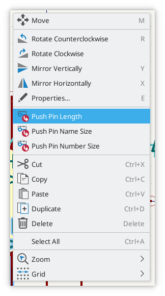
Defining Pins for Multiple Units and Alternate Symbolic Representations
Symbols with multiple units and/or graphical representations are particularly problematic when creating and editing pins. The majority of pins are specific to each symbol unit (because each unit has a different set of pins) and to each body style (because the form and position is different between the normal body style and the alternate form).
The symbol library editor allows the simultaneous creation of pins. By default,
changes made to a pin are made for all units of a multiple unit symbol and to
both representations for symbols with an alternate symbolic representation.
The only exception to this is the pin’s graphical type and name, which remain
unlinked between symbol units and body styles. This dependency was established
to allow for easier pin creation and editing in most cases. This dependency can
be disabled by toggling the ![]() icon on the main tool bar. This will allow you to create pins
for each unit and representation completely independently.
icon on the main tool bar. This will allow you to create pins
for each unit and representation completely independently.
Pins can be common or specific to different units. Pins can also be common to both symbolic representations or specific to each symbolic representation. When a pin is common to all units, it only has to drawn once. Pins are set as common or specific in the pin properties dialog.
An example is the output pin in the 7400 quad dual input NAND gate. Since there
are four units and two symbolic representations, there are eight
separate output pins defined in the symbol definition. When creating
a new 7400 symbol, unit A of the normal symbolic representation will
be shown in the library editor. To edit the pin style in the alternate
symbolic representation, it must first be enabled by clicking the
![]() button on the tool bar. To edit the pin number for each unit,
select the appropriate unit using the
drop down control.
button on the tool bar. To edit the pin number for each unit,
select the appropriate unit using the
drop down control.
Pin Table
Another way to edit pins is to use the Pin Table, which is accessible via the
![]() icon. The Pin Table
displays all of the pins in the symbol and their properties in a table view, so
it is useful for making bulk pin changes.
icon. The Pin Table
displays all of the pins in the symbol and their properties in a table view, so
it is useful for making bulk pin changes.
Any pin property can be edited by clicking on the appropriate cell. Pins can be
added and removed with the ![]() and
and
![]() icons, respectively.
icons, respectively.
You can edit the same property for multiple pins simultaneously by grouping
pins. Pins can be automatically grouped by name, or you manually group several
pins by selecting them and clicking Group Selected. Click the
![]() button to clear the manual grouping.
You can also filter the table to only display pins in certain units.
button to clear the manual grouping.
You can also filter the table to only display pins in certain units.
| Columns of the pin table can be shown or hidden by right-clicking on the header row and checking or unchecking additional columns. Some columns are hidden by default. |
The screenshot below shows the pin table for a quad opamp.
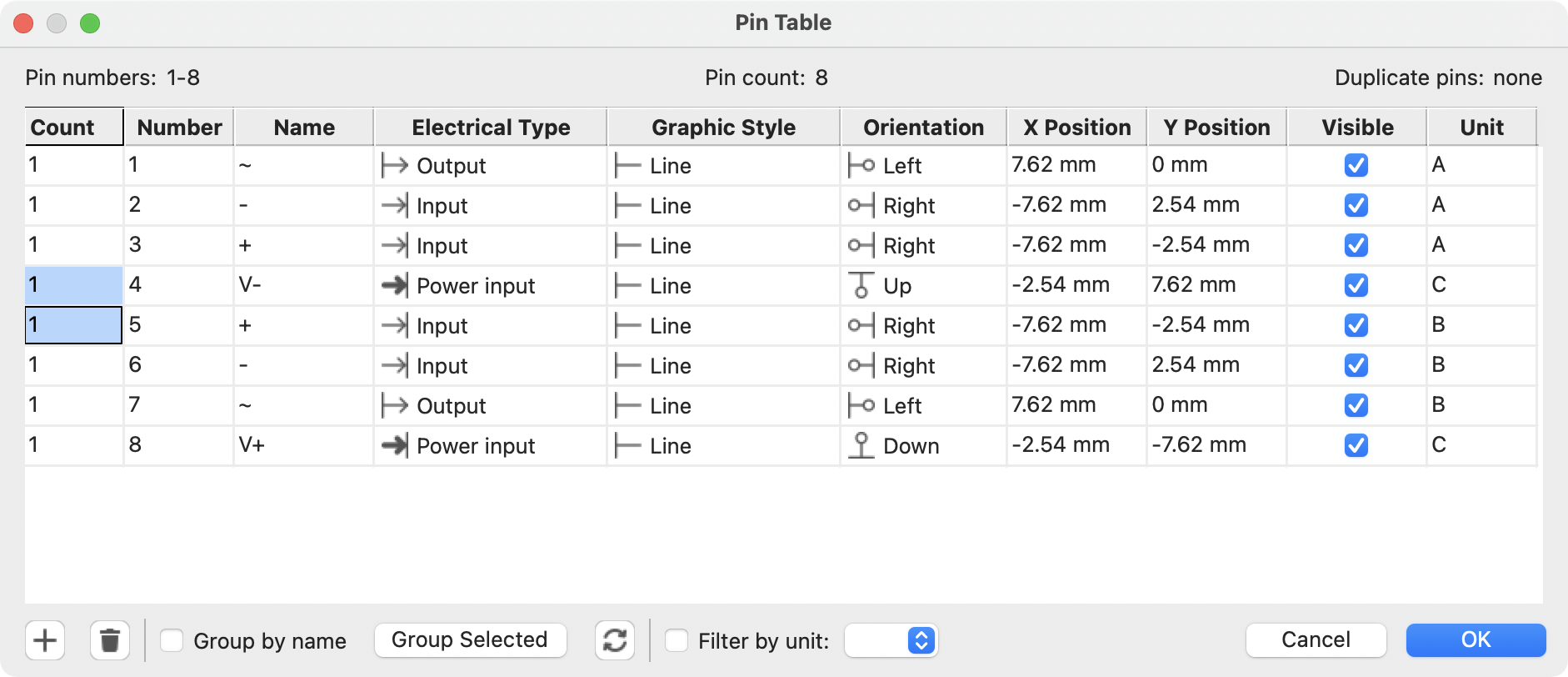
Alternate Pin Definitions
Pins can have alternate pin definitions added to them. Alternate pin definitions allow a user to select a different name, electrical type, and graphical style for a pin when the symbol has been placed in the schematic. This can be used for pins that have multiple functions, such as microcontroller pins.
Alternate pin definitions are added in the Pin Properties dialog as shown below. Each alternate definition contains a pin name, electrical type, and graphic style. This microcontroller pin has all of its peripheral functions defined in the symbol as alternate pin names.
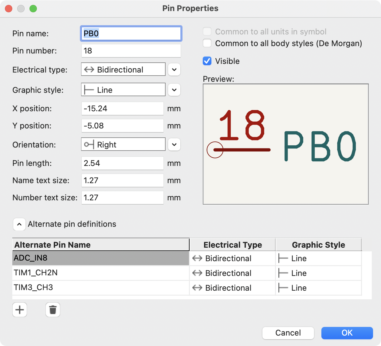
Alternate pin definitions are selected in the Schematic Editor once the symbol has been placed in the schematic. The alternate pin is assigned in the Alternate Pin Assignments tab of the Symbol Properties dialog. Alternate definitions are selectable in the dropdown in the Alternate Assignment column.
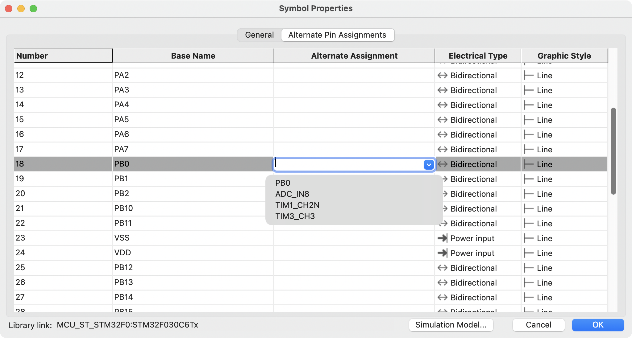
Symbol Fields
All library symbols are defined with four default fields. The reference designator, value, footprint assignment, and datasheet link fields are created whenever a symbol is created or copied. Only the reference designator is required.
The Footprint field, if used, contains a reference to a footprint for the
symbol. The format is LIBNAME:FOOTPRINTNAME, where LIBNAME is the name of
the footprint library in the footprint library table (see the
Footprint Library Table
section in the PCB Editor manual) and FOOTPRINTNAME is the name of the
footprint in the library LIBNAME.
Symbols defined in libraries are typically defined with only these four default fields. Additional fields such as vendor, part number, unit cost, etc. can be added to library symbols but generally this is done in the schematic editor so the additional fields can be applied to all of the symbols in the schematic.
| A convenient way to create additional empty symbol fields is to use define field name templates. Field name templates define empty fields that are added to each symbol when it is inserted into the schematic. Field name templates can be defined globally (for all schematics) in the Schematic Editor Preferences, or they can be defined locally (specific to each project) in the Schematic Setup dialog. |
| If you want to manage a large amount of component data in symbol fields, consider using database libraries. |
Editing Symbol Fields
To edit an existing symbol field, double-click the field, select it or hover and press E, or right-click on the field text and select Properties….
To add new fields, delete optional fields, or edit existing fields, use the
![]() icon on the main tool bar to open the Symbol Properties dialog.
icon on the main tool bar to open the Symbol Properties dialog.
Fields are text information associated with the symbol. Do not confuse them with text in the graphic representation of a symbol.
Creating Power Symbols
Power symbols are symbols that are used to label a wire as part of a global
power net, like VCC or GND. The behavior of power symbols is described in the
electrical connections section. Power symbols are handled and
created the same way as normal symbols, but there are several additional
considerations described below.
It may be useful to place power symbols in a dedicated library. KiCad’s symbol
library places power symbols in the power library, and users may create
libraries to store their own power symbols. If the Define as power symbol box
is checked in a symbol’s properties, that symbol will appear in the Schematic
Editor’s Add Power Symbol dialog for convenient access.
Below is an example of a GND power symbol.
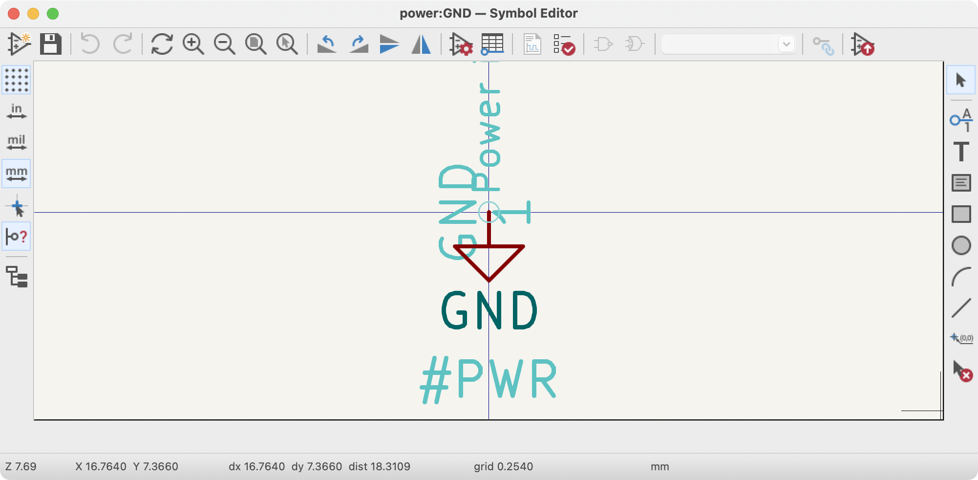
Power symbols consist of a pin of type "Power input" that is marked invisible. They must also have the Define as power symbol property checked. Invisible power input pins have a special property of making implicit global connections based on the pin name.
| If the power symbol has the Define as power symbol property checked, the power input pin does not need to be marked invisible. However, the convention is to make these pins invisible anyway. |
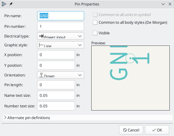
To create a power symbol, use the following steps:
-
Add a pin of type Power input, with Visible unchecked, and the pin named according to the desired net. Make the pin number
1, the length0, and set the graphic style to Line. The pin name establishes the connection to the net; in this case the pin will automatically connect to the netGND. The pin number, length, and line style do not matter electrically. -
Place the pin on the symbol anchor.
-
Use the shape tools to draw the symbol graphics.
-
Set the symbol value. The symbol value does not matter electrically, but it is displayed in the schematic. To eliminate confusion, it should match the pin name (which determines the connected net name).
-
Check the Define as power symbol box in Symbol Properties window. This makes the symbol appear in the Add Power Symbol dialog, makes the
Valuefield read-only in the schematic, prevents the symbol from being assigned a footprint, and excludes the symbol from the board, BOM, and netlists. -
Set the symbol reference and uncheck the Show box. The reference text is not important except for the first character, which should be
#. For the power symbol shown above, the reference could be#GND. Symbols with references that begin with#are not added to the PCB, are not included in Bill of Materials exports or netlists, and they cannot be assigned a footprint in the footprint assignment tool. If a power symbol’s reference does not begin with#, the character will be inserted automatically when the annotation or footprint assignment tools are run.
An easier method to create a new power symbol is to use another symbol as a starting point, as described earlier.
| The connected net name is determined by the power symbol’s pin name, not the name or value of the symbol. When modifying an existing power symbol, make sure to rename the pin so that the new symbol connects to the appropriate power net. This means that power symbol net names can only be changed in the symbol editor, not in the schematic. |
Checking Symbols
The Symbol Editor can check for common issues in your symbols. Run the symbol
checker using the ![]() button in
the top toolbar.
button in
the top toolbar.
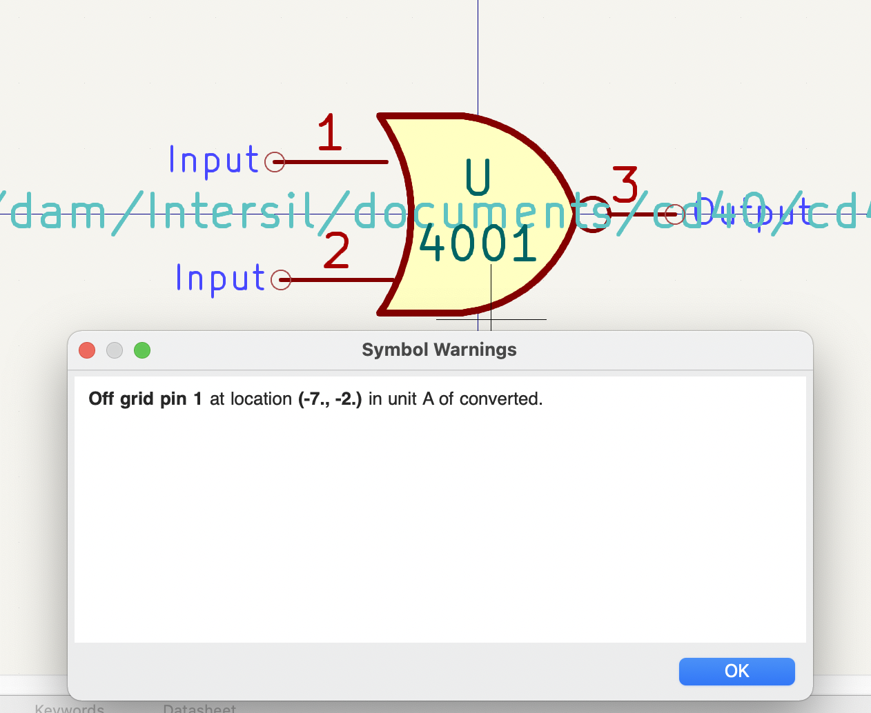
The symbol checker checks for:
-
Pins that are off-grid
-
Pins that are duplicated between symbol units
-
Incorrectly designed power symbols. Power symbols should have:
-
A single unit
-
No alternate body styles
-
A single pin which is either of type Power Output (see PWR_FLAG) or invisible and of type Power Input (see power symbols)
-
-
Illegal reference designator prefixes: reference designator prefixes should not end with a number or
? -
Hidden Power Input pins in non-power symbols: these create implicit connections and are not recommended
Browsing symbol libraries
The Symbol Library Browser allows you to quickly examine the contents of symbol
libraries. The Symbol Library Viewer can be accessed by clicking
![]() icon on the main
toolbar, View → Symbol Library Browser, or clicking Select With
Browser in the Choose Symbol window.
icon on the main
toolbar, View → Symbol Library Browser, or clicking Select With
Browser in the Choose Symbol window.
To examine the contents of a library, select a library from the list on the left hand pane. All symbols in the selected library will appear in the second pane. Select a symbol name to view the symbol.
Double clicking the name of a symbol or using the
![]() button adds the symbol to the schematic.
button adds the symbol to the schematic.
The top toolbar contains the following commands:
|
Open the selected symbol in the Choose Symbol window. |
|
Select previous symbol in library. |
|
Select next symbol in library. |
|
Zoom tools. |
|
Select standard or alternate De Morgan representation of symbol, if applicable. |
|
Select the unit of a multi-unit symbol. |
|
Open the symbol’s datasheet, if it is defined. |
|
Insert current symbol into the schematic. |
Simulator
KiCad provides an embedded electrical circuit simulator using ngspice as the simulation engine. All but the simplest simulations will require you to add simulation models to your symbols before you can simulate your schematic.
When working with the simulator, the official Simulation_SPICE symbol library
may be useful. It contains common symbols used for simulation, like
voltage/current sources and transistors with pins numbered to match the ngspice
node order specification.
KiCad includes a few demo projects to illustrate the simulator’s capabilities.
They can be found in the demos/simulation directory.
Value notation
The simulator supports several notations for writing numerical values:
-
Plain notation :
10100,0.003, -
Scientific notation:
1.01e4,3e-3, -
Prefix notation:
10.1k,3m. -
RKM notation:
4k7,10R.
You can mix prefix and scientific notations. As such, 3e-4k is a
valid input and is equivalent to 0.3. The list of valid prefixes is shown
below. The prefixes are case sensitive.
| Prefix | Meaning | Value |
|---|---|---|
a |
atto |
10-18 |
f |
femto |
10-15 |
p |
pico |
10-12 |
n |
nano |
10-9 |
u |
micro |
10-6 |
m |
milli |
10-3 |
k |
kilo |
103 |
M |
mega |
106 |
G |
giga |
109 |
T |
tera |
1012 |
P |
peta |
1015 |
E |
exa |
1015 |
Raw SPICE Element models and directives are
passed to ngspice directly, without KiCad reformatting the values for ngspice to
consume. Ngspice uses a different, case-insensitive notation: 1 mega (106) is
denoted there as 1Meg, while 1M is 1 milli (10-3). Depending on the
compatibility mode selected, ngspice may not support the same value notations as
KiCad, so care should be taken when using raw SPICE elements and simulation
directives.
|
Assigning models
You need to assign simulation models to symbols before you can simulate your circuit.
Each symbol can have only one model assigned, even if the symbol consists of multiple units. For symbols with multiple units, you should assign the model to the first unit.
SPICE model information is stored as text in symbol fields. Therefore you may define it in either the symbol editor or the schematic editor. To assign a simulation model to a symbol, open the Symbol Properties dialog and click the Simulation Model… button, which opens the Simulation Model Editor dialog.
You can exclude a symbol from simulation entirely by checking the exclude from simulation checkbox in the Symbol Properties dialog.
Inferred models
Resistor, inductor, and capacitor models can be inferred, which means that KiCad
will detect that they are passives and automatically assign an appropriate
simulation model. Therefore they do not require any special settings; users only
need to set the Value field of the symbol.
KiCad infers simulation models for symbols based on the following criteria:
-
The symbol has exactly two pins,
-
The reference designator begins with
R,LorC.
Inferred models are ideal models. If the simulation requires a non-ideal model, you must explicitly assign a model.
Built-in models
KiCad offers several standard simulation models. They do not require an external model file. The following devices are available:
-
Resistors (including potentiometers), capacitors, inductors
-
Transmission lines
-
Switches
-
Voltage and current sources
-
Diodes
-
Transistors (BJT, MOSFET, MESFET, and JFET)
-
Raw SPICE elements
To add a built-in model to a symbol, open the Simulation Model Editor dialog (Symbol Properties → Simulation Model…) and select Built-in SPICE model.
Refer to the ngspice documentation for more details about these models.
Device sets the type of device to simulate: a resistor, BJT, voltage source,
etc. This value is stored in the symbol’s Sim.Device field.
Type selects the type of model to use for the device. Most devices have
several types of models to choose from, which may vary in their degree of
accuracy, which characteristics they are optimized for, and what parameters they
have available. Refer to the ngspice documentation for details. This value is
stored in the symbol’s Sim.Type field.
The parameters tab displays the parameters of the model and lets you edit
them. For example, a resistor’s resistance, a voltage source’s waveform, a
MOSFET’s width and length, etc. Any parameters that differ from the model’s
defaults are stored in the symbol’s Sim.Params field.
The code tab displays the generated SPICE model as it will be written to the SPICE netlist for simulation.
The Save parameter '<parameter name>' in Value field checkbox uses the
symbol’s Value field for storing parameters instead of the Sim.Params field.
This may make it easier to edit simple models from the schematic, without
opening the Simulation Model Editor. This option is only available for ideal
passive models (R, L, C) and DC sources. If the field Sim.Params exists in the
symbol, it will take priority over the Value field.
Library models
KiCad can load SPICE models from external files. The models must be in a standard SPICE format and not encrypted.
To load a model from an external file, open the Simulation Model Editor dialog (Symbol Properties → Simulation Model…) and select SPICE model from file.
File is the path to the model file to use. The path can be absolute or
relative to the project folder. The path can also be relative to the value of
SPICE_LIB_DIR if you have
defined that path variable.
The library filename is saved in the symbol’s Sim.Library field.
Model is the name of the desired model in the model file. If the file
contains multiple models, they will all be listed in the dropdown. The selected
model is listed in the symbol’s Sim.Name field.
Parameters can be overridden (or additional parameters specified) using
the parameters tab. All parameters specified in the selected model or the
parameters tab are stored in the symbol’s Sim.Params field.
The code tab displays the generated SPICE model as it will be written to the SPICE netlist for simulation.
| KiCad does not ship with SPICE models for symbols. SPICE models are usually available from device manufacturers. |
Library models (IBIS)
IBIS (I/O Buffer Information Specification) files are an alternative to SPICE
models for modeling the behavior of input/output buffers on digital parts. In
order to load an IBIS file, users should follow the procedure for SPICE library
models, but provide a .ibs file.
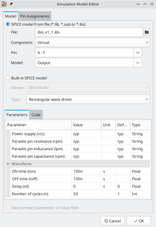
File is the path to the model file to use. The path can be absolute or
relative to the project folder. The path can also be relative to the value of
SPICE_LIB_DIR if you have
defined that path variable.
The library filename is saved in the symbol’s Sim.Library field. If an IBIS
model file is loaded, the remaining fields in the dialog will relate to the IBIS
model.
Component selects which component from the IBIS file to use, as IBIS files
can contain multiple components. The component name is saved in the symbol’s
Sim.Name field.
Pin selects which pin in the IBIS model to simulate. The selected pin must
be mapped to a symbol pin in the Pin Assignments tab. The chosen pin’s
number is saved in the symbol’s Sim.Ibis.Pin field.
Model is the list of models available for the selected pin, for example an
input or an output. The chosen model name is saved in the symbol’s
Sim.Ibis.Model field.
Type selects what the pin should do in the simulation. A pin can be a passive
device that doesn’t drive any value; it can be a DC driver that drives
high, low, or high-impedance; or it can be a rectangular wave or
PRBS driver. This value is stored in the symbol’s Sim.Type field.
The Parameters tab lets you see and edit the parameters of the model. For
each parameter, you can switch between a minimum, typical, or maximum value, as
defined in the IBIS file. You can also choose the parameters of the driven
waveform, depending on the pin’s chosen type. Any parameters that differ
from the defaults are stored in the symbol’s Sim.Params field.
| KiCad does not ship with IBIS models for symbols. IBIS models are usually available from device manufacturers. |
KiCad’s Simulation_SPICE symbol library provides several symbols that may be
useful for IBIS simulations. IBIS_DEVICE can be used for device (input) pins,
while IBIS_DRIVER can be used for simulating driver pins. There are also
variants of each for differential pins.
|
Pin Assignment
Simulation models may have their pins numbered differently than the corresponding symbol. For example, SPICE models for diodes usually consider pin 1 to be the anode, while schematic symbols are usually drawn with pin 1 as the cathode.
You can use the Simulation Model Editor’s Pin Assignments tab to map the symbol’s pins to the simulation model pins.
| Always make sure symbol pins are correctly mapped to simulation model pins. |
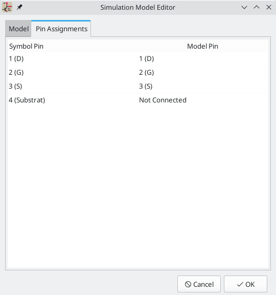
The left column displays the name and number of each symbol pin. For each symbol pin, you can select the corresponding pin from the simulation model in the dropdown in the right column.
When you use a subcircuit model, the dialog displays the model’s code under the pin assignments for use as a reference while assigning pins.
SPICE directives
It is possible to add SPICE directives by placing them in text fields on a schematic sheet. This approach is convenient for defining the default simulation type. The list of supported directives in text fields is:
-
Directives starting with a dot (e.g.
.tran 10n 1m) -
Coupling coefficients for inductors (e.g.
K1 L1 L2 0.89)
It is not possible to place additional components using text fields.
If a simulation command is included in schematic text, the simulator will use it as the simulation command when you open the simulator. However, you can override it in the Simulation Command dialog.
Refer to the ngspice documentation for more details about SPICE directives.
Running simulations
User Interface
To run a simulation, open the SPICE simulator dialog by clicking
Inspect → Simulator in the schematics editor window or using the
![]() button in the top toolbar.
button in the top toolbar.
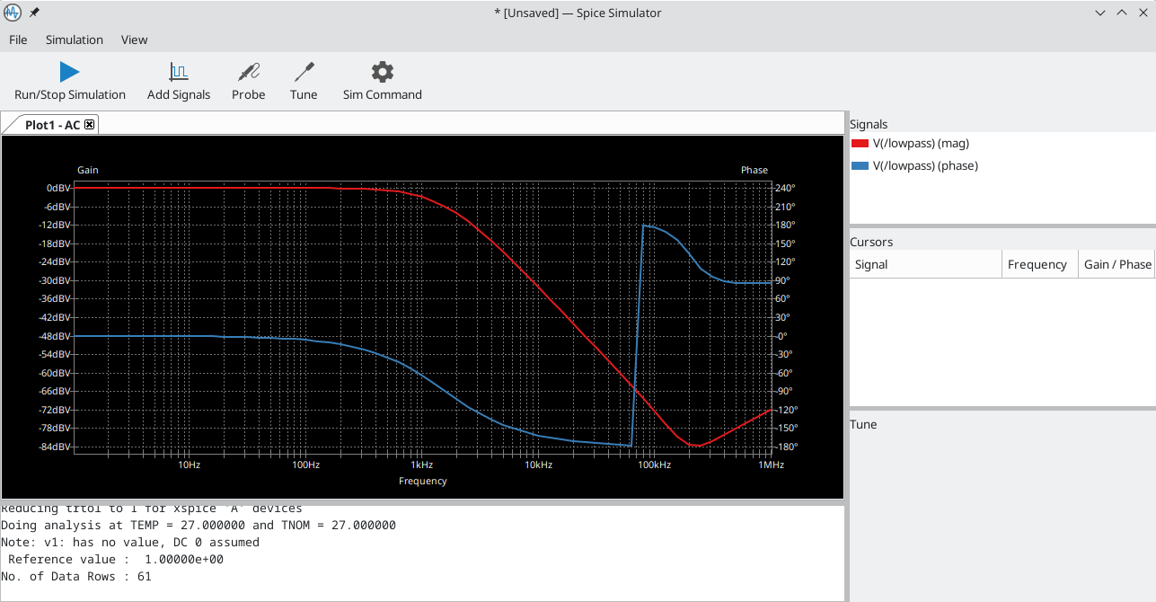
The dialog is divided into several sections:
-
The top of the window has a toolbar with buttons for commonly used actions.
-
The main part of the window graphically shows the simulation results. Signals need to be probed before they are displayed in the plot.
-
Below the plot panel, the output console shows logs from the ngspice simulation engine.
-
The right side of the window displays a list of plotted signals, a list of active cursors, and a tuning tool for adjusting component values based on simulation results.
Workbooks
Workbooks are files that store information about the simulation environment, including simulation setup parameters and the list of displayed signals. They can be used to store the setup for a set of analyses, which can then be reloaded and rerun at a later time.
You can save and load a workbook using File → Save Workbook and File → Open Workbook.
| Workbooks store simulation setup information, but they do not store simulation results. You can export simulation results to PNG (graphics) or CSV (data points) with File → Export Current Plot as PNG… and File → Export Current Plot as CSV…. |
Running a Simulation
Before running a simulation, you need to select a simulation type and choose the
simulation parameters. This can be done using Simulation → Settings…
or the Sim Command button (![]() ) and then
selecting one of the available analysis types:
) and then
selecting one of the available analysis types:
-
AC
-
DC Transfer
-
Operating Point
-
Transient
-
Custom
Analysis types are further explained in the ngspice documentation.
An alternative way to configure a simulation is to type SPICE directives into text fields on schematics. Any text field directives related to a simulation command are overridden by the settings selected in the dialog. This means that once a simulation has run, the dialog overrides the schematic directives until the simulator is reopened.
Once the simulation command is set, users can start a simulation with
Simulation → Start Simulation (Ctrl+R) or the
Run/Stop Simulation button
(![]() ).
).
AC analysis
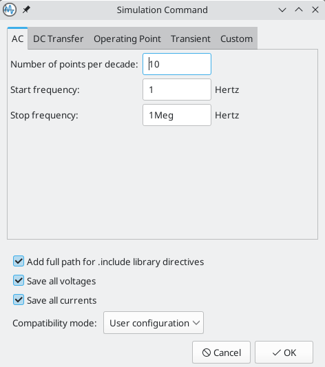
Calculates the small signal AC behavior of the circuit in response to a stimulus. Performs a decade sweep of stimulus frequency.
To run an AC analysis, you must choose a number of points to measure per decade and the start and end frequencies for the decade sweep.
The output is displayed as a Bode plot (output magnitude and phase vs. a decade sweep of stimulus frequency).
DC transfer analysis
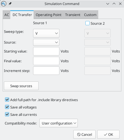
Calculates the DC behavior of the circuit while sweeping one or two sources (voltage or current), resistors, or the simulation temperature.
To run a DC analysis, you must choose what type of sweep(s) to perform, which source, resistor, or temperature value(s) to sweep, and what the sweep range(s) and step(s) should be.
The output is displayed as a plot.
Operating point analysis
Calculates the DC operating point of the circuit. This analysis has no options, and results are printed to the SPICE log.
Transient analysis
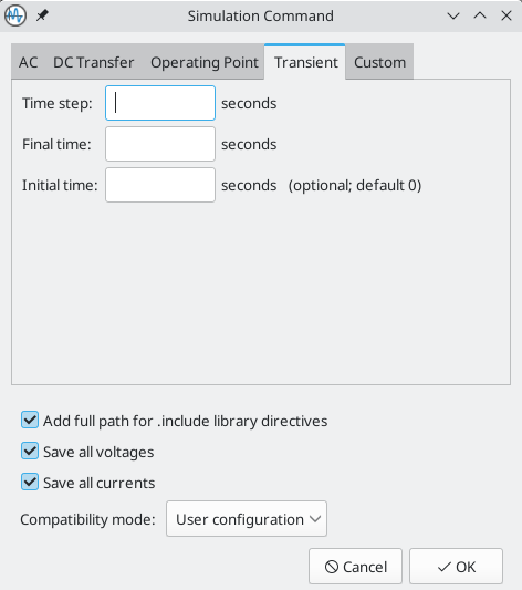
Calculates the time-varying behavior of the circuit.
To run a transient analysis, you need to specify a suggested time step and a final simulation time. You can optionally specify a starting time to override the default of 0.
The output is displayed as a plot.
Custom analysis
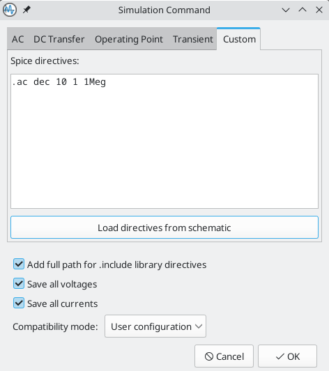
A custom analysis lets you write SPICE commands to set up the analysis. Press the Load directives from schematic button to copy any SPICE directives in schematic text into the custom analysis textbox.
Refer to the ngspice documentation for more information about analysis commands.
Additional simulation settings
There are several simulation options that apply to all types of simulations.
Add full path for .include library directives controls whether to convert
relative paths to absolute in .include directives in schematic text.
Save all voltages and Save all currents controls whether the simulator saves voltages and currents, respectively, for internal nodes of devices. When unchecked, the simulator only saves voltages and currents for external nodes.
The Compatibility mode dropdown selects the compatibility mode that the
simulator uses to load models. The User configuration option refers to the
user’s .spiceinit ngspice configuration file. Compatibility modes are
described in the ngspice documentation.
Probing signals
Using the signal list
You can display a list of available signals with Simulation →
Add signals (Ctrl+A hotkey or
![]() button). Double
clicking an element in the list will add it to list of probed signals. Several
signals can be selected at once using the Ctrl / Shift keys.
button). Double
clicking an element in the list will add it to list of probed signals. Several
signals can be selected at once using the Ctrl / Shift keys.
Using the probe tool
A probe tool is available in the toolbar of the simulator window
(![]() ), which provides a user-friendly way of
selecting signals for plotting. When activated, users can click elements in the
schematic editor. To probe a voltage, click a wire with the probe tool. When
hovering over wires with the tool, the corresponding net is highlighted. To
probe a current, click on a symbol pin. When hovering over a pin, the cursor
will change from a voltage probe symbol to a current clamp symbol. It is not
possible to probe power signals with this tool.
), which provides a user-friendly way of
selecting signals for plotting. When activated, users can click elements in the
schematic editor. To probe a voltage, click a wire with the probe tool. When
hovering over wires with the tool, the corresponding net is highlighted. To
probe a current, click on a symbol pin. When hovering over a pin, the cursor
will change from a voltage probe symbol to a current clamp symbol. It is not
possible to probe power signals with this tool.
Using a SPICE directive
While ngspice supports the .plot directive, it cannot be used in current
versions of KiCad.
Differential voltage
Probing differential voltages usually requires a simulation symbol. One is
available in Simulation_SPICE:VOLTMETER_DIFF in the official libraries. This
symbol has two terminals for differential voltage sensing, and one the user can
probe.
A SPICE model called kicad_builtin_vdiff is preassigned to the built-in
VOLTMETER_DIFF symbol. Users should not define a SPICE model with the same
name.
|
It is also possible to probe across two-terminal devices such as a resistor by
placing the .probe vd(X) directive, where X is the name of the device (such
as R1). Then in order to probe it, enter vd_X when adding a signal using the
list of signals. Note that the signal will not appear in the list of signals, it
should be typed in by the user. This method has the advantage of not adding
extra symbols to the schematic sheet.
Remove a signal probe
In order to remove a signal probe, double click on it in the signal list, or right-click it and select Remove Signal.
Tuning components
It is possible to change passive (R, L, C) values using sliders to graphically
adjust them. Whenever the slider is set to a new position, the simulation is run
with the new parameters and plots are updated. In order to add a slider for a
component, use Simulation → Tune Component Value or the
![]() button in the toolbar, and then
click on the component to tune.
button in the toolbar, and then
click on the component to tune.
-
The top text field sets the maximum component value.
-
The middle text field sets the actual component value.
-
The bottom text field sets the minimum component value.
-
The slider allows the user to modify the component value.
-
The Save button modifies component value on the schematic to the value selected with the slider.
-
The
 button removes the
component from the Tune panel and restores its original value.
button removes the
component from the Tune panel and restores its original value.
Visualizing results
Plotted quantities
This section applies to simulation commands that output vectors such as .ac and .tran.
Simulation results are visualized as plots. There can be multiple plots opened in separate tabs, but only the active one is updated when a simulation is executed. This way it is possible to compare simulation results for different runs.
Plots can be customized by toggling grid and legend visibility using the View menu. When a legend is visible, it can be dragged to change its position. You can toggle the plot background from dark to light with View → White Background and switch current and phase plots to use dotted lines instead of solid with View → Dotted Current/Phase.
For precise measurement, it is possible to add a cursor to a a signal. To do so, right click on a signal name in the Signals pane and select Show Cursor. It is then possible to move the cursor to the point of interest. The values are then shown in the Cursor section of the window. To hide a cursor, right click on a signal and select Hide Cursor. Each signal may have one cursor displayed.
The following interactions are possible with the plot panel:
-
scroll mouse wheel to zoom in/out
-
right click to open a context menu to adjust the view
-
draw a selection rectangle to zoom in the selected area
-
drag a cursor to change its coordinates
Numerical values
Some analysis types, such as the DC operating point analysis (.op), do not
have any graphical output to plot. Instead, their output is printed in the SPICE
console.
Exporting results
KiCad’s simulator offers two ways to export results:
-
As an image using File → Export Current Plot as PNG…
-
As a
.csvfile containing the datapoints using File → Export Current Plot as CSV….
Troubleshooting
Incorrect netlist
It is possible to inspect the SPICE netlist with Simulation → Show SPICE netlist…. This method of troubleshooting requires some SPICE knowledge, but spotting errors in the netlist can help determine the cause of simulation problems.
Simulation error
The output console displays messages from the simulator. It is advised to check the console output to verify there are no errors or warnings.
Convergence problems
In case the simulation does not converge in a reasonable amount of time (or not at all), it is possible to add the following SPICE directives.
| Changing convergence options can lead to erroneous results. These options should be used with caution. |
.options gmin=1e-10
.options abstol=1e-10
.options reltol=0.003
.options cshunt=1e-15
-
gminis the minimum conductance allowed by the program. The default value is1e-12. -
abstolis the absolute current error tolerance of the program. The default value is 1 pA. -
reltolis the relative error tolerance of the program. The default value is0.001(0.1%). -
cshuntadds a capacitor from each voltage node in the circuit to ground.
Advanced Topics
Configuration and Customization
| This section of the KiCad documentation has not yet been written. We appreciate your patience as our small team of volunteer documentation writers work to update and expand the documentation. |
Text variables
KiCad supports text variables, which allow you to substitute the variable name
with a defined text string. This substitution happens anywhere the variable name
is used inside the variable replacement syntax of ${VARIABLENAME}.
You can define your own text variables in the schematic or board setup dialogs, but there are also a number of built-in system text variables. System text variables may be available in some contexts and not others.
The following variables can be used in schematic text, label names, label fields, hierarchical sheet fields, symbol text, and symbol fields. There are also a number of variables that can be used in the PCB Editor.
Variables used in hierarchical sheet fields refer to the properties of the
hierarchical sheet, not the parent, unless otherwise noted. For example, ${#}
returns the subsheet’s page number when used in a hierarchical sheet field, but
the parent sheet’s page number when used in graphic text in the parent sheet.
| Variable name | Description |
|---|---|
|
Sheet number. |
|
Total number of schematic sheets. |
|
Sheet path of the current sheet. |
|
Filename of the root schematic sheet, with a file extension. |
|
Project name, without a file extension. |
|
Contents of drawing sheet’s |
|
Today’s date, in ISO format. |
|
Contents of drawing sheet’s |
|
Contents of drawing sheet’s |
|
Contents of drawing sheet’s |
|
Contents of drawing sheet’s |
|
Contents of project text variable
|
|
Contents of symbol field, hierarchical sheet field, or label field
Both built-in and user-defined fields are available. Built-in fields use all
uppercase letters: for example, to access a symbol’s value, use Built-in symbol fields are Built-in sheet fields are Built-in label fields are |
|
Contents of field Both built-in and user-defined fields are available. Built-in fields use all
uppercase letters: for example, to access the value of Built-in symbol fields are |
Database Libraries
A database library is a type of KiCad symbol library that holds data about parts in an external SQL database. Database libraries do not contain any symbol or footprint definitions by themselves. Instead, they reference symbols and footprints found in other KiCad libraries. Each database library entry maps a KiCad symbol (from another library) to a set of properties (fields) and usually a KiCad footprint (from a footprint library).
Using database libraries allows you to create fully-defined parts (sometimes called atomic parts) out of KiCad symbols and footprints without needing to store all the part properties in a symbol library. The external database can be linked to third-party tools for managing part data and lifecycles. Database library workflows are generally more complex than the standard KiCad library workflows, and so this type of library is typically only used in situations where it makes managing a large library of fully-defined parts more efficient (such as in organization or team settings).
KiCad does not provide a GUI for editing a SQL database or defining a database library. It is up to the user to find the most appropriate workflow and toolchain for creating and updating the database itself. Some users may want to directly edit the database through a third-party database client, and some may use other third-party software such as a part lifecycle management (PLM) tool to create and edit data.
In a database library, there are one or more tables that generally represent a single type of
part (such as Resistors or Capacitors). Each table can have an independent schema, meaning that
different types of parts can have different properties that are translated into symbol fields in
KiCad. Each table must have a unique ID column which is used as the identifier for a symbol placed
from that table. This unique ID will typically be a part number (either a manufacturer’s part
number, or an internal organization part number). Each table must also have a column that contains
a mapping to a KiCad symbol, in the form LibraryNickname:SymbolName. The LibraryNickname must
match a symbol library that is present in the KiCad library tables. Tables may also contain a
column containing a KiCad footprint, in the form LibraryNickname:FootprintName. If this column
is present, symbols placed from the table will include a footprint mapping.
Tables may also contain arbitrary additional columns that may optionally be mapped to symbol fields in KiCad. The KiCad database library configuration file controls how these fields should be named, whether or not to make the fields visible, and whether or not to include the fields in the data displayed in the Symbol Chooser.
Database Library Configuration Files
To create a database library, you must create a configuration file that contains the necessary
information for KiCad to connect to your database and retrieve data from tables. Copy the template
below into a new file and save it with a kicad_dbl extension. You can then add this file to your
global symbol library table using the Configure Symbol Libraries dialog.
{
    "meta": {
        "version": 0
    },
    "name": "My Database Library",
    "description": "A database of components",
    "source": {
        "type": "odbc",
        "dsn": "",
        "username": "",
        "password": "",
        "timeout_seconds": 2,
        "connection_string": ""
    },
    "libraries": [
        {
            "name": "Resistors",
            "table": "Resistors",
            "key": "Part ID",
            "symbols": "Symbols",
            "footprints": "Footprints",
            "fields": [
                {
                    "column": "MPN",
                    "name": "MPN",
                    "visible_on_add": false,
                    "visible_in_chooser": true,
                    "show_name": true,
                    "inherit_properties": true
                },
                {
                    "column": "Value",
                    "name": "Value",
                    "visible_on_add": true,
                    "visible_in_chooser": true,
                    "show_name": false
                }
            ],
            "properties": {
                "description": "Description",
                "footprint_filters": "Footprint Filters",
                "keywords": "Keywords",
                "exclude_from_bom": "No BOM",
                "exclude_from_board": "Schematic Only"
            }
        }
    ]
}
Configuring the source
KiCad currently only supports ODBC connections to SQL databases. You can either connect with a
DSN or a connection string. If a DSN name is supplied, the optional username and password
fields will be used to connect to the DSN. If a connection string is supplied, the dsn,
username, and password fields are ignored. The connection string will be passed directly to
the ODBC driver, so you can include any parameters your ODBC driver supports.
KiCad does not recommend or endorse any particular ODBC driver or database server, but has been tested to work with Sqlite, MySQL, MariaDB, and PostgreSQL.
Flatpak users: Due to Flatpak sandboxing, the only way to connect to database servers
running on your local machine is via TCP/IP. Using the default UNIX domain socket connections
for i.e. MySQL, MariaDB, or PostgreSQL is not possible. First, make sure that your database
server allows TCP/IP connections, and then add the required Port parameter to your connection
string. For example, add Port=3306; for the default TCP port of MySQL/MariaDB, or
Server=localhost;Port=5432; to force PostgreSQL to use a TCP connection to the local server.
|
Configuring libraries
Each database library can contain "sub-libraries" mapped to a single database table. The
libraries entry in the configuration file contains a list of objects that each define a single
library. The following settings must exist for each library:
name: The name of the table that will be shown in the KiCad UI.
table: The name of the table in the database.
key: The column name containing a unique key that will be used to identify parts from the table.
symbols: The column name containing KiCad symbol references.
footprints: The column name containing KiCad footprint references.
fields: A list of field definitions. Each field defined here will be added to the symbol when
it is placed on the schematic. If a field with a matching name is already defined in the source
symbol, the value from the database table will override whatever value was defined in the source
symbol. Each field definition may contain:
column: The name of the database table column that should be mapped to a field.
name: The name of the KiCad field to populate from the database.
visible_on_add: If true, this field will be visible in the schematic when a symbol is added. If
this setting is not specified, it will default to false.
visible_in_chooser: If true, this field will be shown in the Symbol Chooser as a column. If
this setting is not specified, it will default to false.
show_name: If true, the field’s name will be shown in addition to its value in the schematic.
If this setting is not specified, it will default to false.
inherit_properties: If true, and a field with the given name already exists on the source
symbol, only the field contents will be updated from the database, and the other properties
(visible_on_add, show_name, etc) will be kept as they were set in the source symbol. If the
given field name does not exist in the source symbol, this setting is ignored. If this setting is
not specified, it will default to false.
properties: A map of symbol properties to database columns. All properties are optional; any
that are not specified in the database library configuration will be inherited from the values set
for the source symbol. The following properties are supported:
description: The symbol’s Description property.
footprint_filters: Reserved for future expansion.
keywords: The symbol’s Keywords property.
exclude_from_bom: The symbol’s "Exclude from Bill of Materials" setting. The column named here
must be a numeric type, and will be taken as a boolean (0 for false, 1 for true).
exclude_from_board: The symbol’s "Exclude from PCB" setting. The column named here must be a
numeric type, and will be taken as a boolean (0 for false, 1 for true).
Database columns may be mapped to custom (user-defined) fields, or to certain built-in KiCad
fields, including Value and Datasheet.
Using database libraries
After creating your configuration file and adding it to your symbol library table, you can place parts from the database tables using the Symbol Chooser. Parts placed from a database library can be updated using the Update Symbols from Library function, which will update any fields that were changed in the database as well as updating the underlying symbol if it was changed in the source library.
Note that any source library referenced by a database table must also be present in the symbol library table for the database library to function. If you want to use a library only as a source of symbols for a database library, you can hide it from the Symbol Chooser by clearing the "Visible" checkbox in the Manage Symbol Libraries dialog.
Custom Netlist and BOM Formats
KiCad can output netlists and BOMs in various formats, and users can define new formats if desired.
The process of exporting a netlist is described in the netlist export section. BOM output is described in the BOM export section.
The following section describes how to create an exporter for a new output format.
Adding new netlist generators
New netlist generators are added to the Export Netlist dialog by clicking the Add Generator… button.
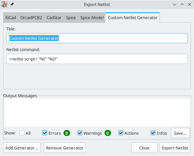
New generators require a name and a command. The name is shown in the tab label, and the command is run whenever the Export Netlist button is clicked.
When the netlist is generated, KiCad creates an intermediate XML file which contains all of the netlist information from the schematic. The generator command is then run in order to transform the intermediate netlist into the desired netlist format.
The netlist command must be set up properly so that the netlist generator script takes the intermediate netlist file as input and outputs the desired netlist file. The exact netlist command will depend on the generator script used. The command format is described below.
Python and XSLT are commonly used tools to create custom netlist generators.
Adding a new BOM generator
KiCad also uses the intermediate netlist file to generate BOMs with the Generate BOM tool.
Additional scripts can be added to the list of BOM generator scripts by clicking
the ![]() button. Scripts can be
removed by clicking the
button. Scripts can be
removed by clicking the ![]() button. The
button. The ![]() button opens the
selected script in a text editor.
button opens the
selected script in a text editor.
Generator scripts written in Python and XSLT can contain a header comment that
describes the generator’s functionality and usage. This header comment is
displayed in the BOM dialog as the description for each generator. The header
comment must contain the string @package. Everything following that string
until the end of the comment is used as the description for the generator.
KiCad automatically fills the command line field when a new generator script is added, but the command line might need to be adjusted by hand depending on the generator script. KiCad attempts to automatically determine the output file extension from the example command line in the generator script’s header.
Generator command line format
The command line for a netlist or BOM exporter defines the command that KiCad will run to generate the selected output file.
For a netlist exporter using xsltproc, an example is:
xsltproc -o %O.net /usr/share/kicad/plugins/netlist_form_pads-pcb.asc.xsl %I
For a BOM exporter using Python, an example is:
/usr/bin/python3 /usr/share/kicad/plugins/bom_csv_grouped_by_value.py "%I" "%O.csv"
It is recommended to surround arguments in the command line with quotes
(") in case they contain spaces or other special characters.
|
Some character sequences like %I and %O have a special meaning in the
command line, because KiCad replaces them with a filename or path before
executing the command.
| Parameter | Replaced with… | Description |
|---|---|---|
|
|
Absolute path and filename of the intermediate netlist file, which is the input to the BOM or netlist generator plugin |
|
|
Absolute path and filename of the output BOM or netlist file (without file
extension). An appropriate file extension may need to be specified after the
|
|
|
Base filename of the output BOM or netlist file (without path or file
extension). An appropriate file extension may need to be specified after the
|
|
|
Absolute path of the project directory, without trailing slash. |
Intermediate Netlist File
When exporting BOM files and netlists, KiCad creates an intermediate netlist file and then runs a separate tool which post-processes the intermediate netlist into the desired netlist or BOM format.
The intermediate netlist uses XML syntax. It contains a large amount of data about the design. Depending on the output (BOM or netlist), different subsets of the complete intermediate netlist file will be included in the final output file.
The structure of the intermediate netlist file is described in detail below.
Because the conversion from intermediate netlist file to output netlist or BOM is a text-to-text transformation, the post-processing filter can be written using Python, XSLT, or any other tool capable of taking XML as input.
XSLT is not recommended for new netlist or BOM exporters; Python or
another tool should be used instead. Beginning with KiCad 7, xsltproc is no
longer installed with KiCad, although it can be installed separately.
Nevertheless, several examples of netlist exporters using XSLT are included
below.
|
Intermediate Netlist structure
This sample gives an idea of the netlist file format.
<?xml version="1.0" encoding="utf-8"?>
<export version="D">
  <design>
    <source>F:\kicad_aux\netlist_test\netlist_test.sch</source>
    <date>29/08/2010 21:07:51</date>
    <tool>eeschema (2010-08-28 BZR 2458)-unstable</tool>
  </design>
  <components>
    <comp ref="P1">
      <value>CONN_4</value>
      <libsource lib="conn" part="CONN_4"/>
      <sheetpath names="/" tstamps="/"/>
      <tstamps>4C6E2141</tstamps>
    </comp>
    <comp ref="U2">
      <value>74LS74</value>
      <libsource lib="74xx" part="74LS74"/>
      <sheetpath names="/" tstamps="/"/>
      <tstamps>4C6E20BA</tstamps>
    </comp>
    <comp ref="U1">
      <value>74LS04</value>
      <libsource lib="74xx" part="74LS04"/>
      <sheetpath names="/" tstamps="/"/>
      <tstamps>4C6E20A6</tstamps>
    </comp>
    <comp ref="C1">
      <value>CP</value>
      <libsource lib="device" part="CP"/>
      <sheetpath names="/" tstamps="/"/>
      <tstamps>4C6E2094</tstamps>
    <comp ref="R1">
      <value>R</value>
      <libsource lib="device" part="R"/>
      <sheetpath names="/" tstamps="/"/>
      <tstamps>4C6E208A</tstamps>
    </comp>
  </components>
  <libparts/>
  <libraries/>
  <nets>
    <net code="1" name="GND">
      <node ref="U1" pin="7"/>
      <node ref="C1" pin="2"/>
      <node ref="U2" pin="7"/>
      <node ref="P1" pin="4"/>
    </net>
    <net code="2" name="VCC">
      <node ref="R1" pin="1"/>
      <node ref="U1" pin="14"/>
      <node ref="U2" pin="4"/>
      <node ref="U2" pin="1"/>
      <node ref="U2" pin="14"/>
      <node ref="P1" pin="1"/>
    </net>
    <net code="3" name="">
      <node ref="U2" pin="6"/>
    </net>
    <net code="4" name="">
      <node ref="U1" pin="2"/>
      <node ref="U2" pin="3"/>
    </net>
    <net code="5" name="/SIG_OUT">
      <node ref="P1" pin="2"/>
      <node ref="U2" pin="5"/>
      <node ref="U2" pin="2"/>
    </net>
    <net code="6" name="/CLOCK_IN">
      <node ref="R1" pin="2"/>
      <node ref="C1" pin="1"/>
      <node ref="U1" pin="1"/>
      <node ref="P1" pin="3"/>
    </net>
  </nets>
</export>
General netlist file structure
The intermediate Netlist accounts for five sections.
-
The header section.
-
The components section.
-
The lib parts section.
-
The libraries section.
-
The nets section.
The file content has the delimiter <export>
<export version="D">
...
</export>
The header section
The header has the delimiter <design>
<design>
<source>F:\kicad_aux\netlist_test\netlist_test.sch</source>
<date>21/08/2010 08:12:08</date>
<tool>eeschema (2010-08-09 BZR 2439)-unstable</tool>
</design>
This section can be considered a comment section.
The components section
The component section has the delimiter <components>
<components>
<comp ref="P1">
<value>CONN_4</value>
<libsource lib="conn" part="CONN_4"/>
<sheetpath names="/" tstamps="/"/>
<tstamps>4C6E2141</tstamps>
</comp>
</components>
This section contains the list of components in your schematic. Each component is described like this:
<comp ref="P1">
<value>CONN_4</value>
<libsource lib="conn" part="CONN_4"/>
<sheetpath names="/" tstamps="/"/>
<tstamps>4C6E2141</tstamps>
</comp>| Element name | Element description |
|---|---|
|
name of the lib where this component was found. |
|
component name inside this library. |
|
path of the sheet inside the hierarchy: identify the sheet within the full schematic hierarchy. |
|
timestamp of the component. |
Note about time stamps for components
To identify a component in a netlist and therefore on a board, the timestamp reference is used as unique for each component. However KiCad provides an auxiliary way to identify a component which is the corresponding footprint on the board. This allows the re-annotation of components in a schematic project and does not lose the link between the component and its footprint.
A time stamp is an unique identifier for each component or sheet in a schematic project. However, in complex hierarchies, the same sheet is used more than once, so this sheet contains components having the same time stamp.
A given sheet inside a complex hierarchy has an unique identifier: its sheetpath. A given component (inside a complex hierarchy) has a unique identifier: the sheetpath and its timestamp.
The libparts section
The libparts section has the delimiter <libparts>, and the content of
this section is defined in the schematic libraries.
<libparts>
<libpart lib="device" part="CP">
  <description>Condensateur polarise</description>
  <footprints>
    <fp>CP*</fp>
    <fp>SM*</fp>
  </footprints>
  <fields>
    <field name="Reference">C</field>
    <field name="Valeur">CP</field>
  </fields>
  <pins>
    <pin num="1" name="1" type="passive"/>
    <pin num="2" name="2" type="passive"/>
  </pins>
</libpart>
</libparts>| Element name | Element description |
|---|---|
|
The symbol’s footprint filters. Each footprint filter is in a separate |
|
The symbol’s fields. Each field’s name and value is given in a separate `<field name="fieldname">…</field> tag. |
|
The symbol’s pins. Each pin is given in a separate |
Possible electrical pin types are:
| Pintype | Description |
|---|---|
Input |
Usual input pin |
Output |
Usual output |
Bidirectional |
Input or Output |
Tri-state |
Bus input/output |
Passive |
Usual ends of passive components |
Unspecified |
Unknown electrical type |
Power input |
Power input of a component |
Power output |
Power output like a regulator output |
Open collector |
Open collector often found in analog comparators |
Open emitter |
Open emitter sometimes found in logic |
Not connected |
Must be left open in schematic |
The libraries section
The libraries section has the delimiter <libraries>. This section
contains the list of schematic libraries used in the project.
<libraries>
  <library logical="device">
    <uri>F:\kicad\share\library\device.lib</uri>
  </library>
  <library logical="conn">
    <uri>F:\kicad\share\library\conn.lib</uri>
  </library>
</libraries>
The nets section
The nets section has the delimiter <nets>. This section describes the
connectivity of the schematic by listing all nets and the pins connected to
each net.
<nets>
  <net code="1" name="GND">
    <node ref="U1" pin="7"/>
    <node ref="C1" pin="2"/>
    <node ref="U2" pin="7"/>
    <node ref="P1" pin="4"/>
  </net>
  <net code="2" name="VCC">
    <node ref="R1" pin="1"/>
    <node ref="U1" pin="14"/>
    <node ref="U2" pin="4"/>
    <node ref="U2" pin="1"/>
    <node ref="U2" pin="14"/>
    <node ref="P1" pin="1"/>
  </net>
</nets>
A possible net contains the following.
<net code="1" name="GND">
  <node ref="U1" pin="7"/>
  <node ref="C1" pin="2"/>
  <node ref="U2" pin="7"/>
  <node ref="P1" pin="4"/>
</net>| Element name | Element Description |
|---|---|
|
an internal identifier for this net |
|
the net name |
|
the pin (identified by |
Example netlist exporters
Some example netlist exporters using XSLT are included below.
XSLT itself is an XML language very suitable for XML transformations.
The xsltproc program can be used to
read the Intermediate XML netlist input file, apply a style-sheet to transform
the input, and save the results in an output file. Use of xsltproc requires a
style-sheet file using XSLT conventions. The full conversion process is handled
by KiCad, after it is configured once to run xsltproc in a specific way.
The document that describes XSL Transformations (XSLT) is available here: http://www.w3.org/TR/xslt
| When writing a new netlist exporter, consider using Python or another tool rather than XSLT. |
PADS netlist example using XSLT
The following example shows how to create an exporter for the PADS netlist
format using xlstproc.
The PADS netlist format is comprised of two sections:
-
A list of footprints
-
A list of nets, together with the pads connected to each net.
Below is an XSL style-sheet which converts the intermediate netlist file to the PADS netlist format.
<?xml version="1.0" encoding="ISO-8859-1"?>
<!--XSL style sheet to Eeschema Generic Netlist Format to PADS netlist format
Copyright (C) 2010, SoftPLC Corporation.
GPL v2.
How to use:
https://lists.launchpad.net/kicad-developers/msg05157.html
-->
<!DOCTYPE xsl:stylesheet [
<!ENTITY nl "
"> <!--new line CR, LF -->
]>
<xsl:stylesheet version="1.0" xmlns:xsl="http://www.w3.org/1999/XSL/Transform">
<xsl:output method="text" omit-xml-declaration="yes" indent="no"/>
<xsl:template match="/export">
<xsl:text>*PADS-PCB*&nl;*PART*&nl;</xsl:text>
<xsl:apply-templates select="components/comp"/>
<xsl:text>&nl;*NET*&nl;</xsl:text>
<xsl:apply-templates select="nets/net"/>
<xsl:text>*END*&nl;</xsl:text>
</xsl:template>
<!-- for each component -->
<xsl:template match="comp">
<xsl:text> </xsl:text>
<xsl:value-of select="@ref"/>
<xsl:text> </xsl:text>
<xsl:choose>
<xsl:when test = "footprint != '' ">
<xsl:apply-templates select="footprint"/>
</xsl:when>
<xsl:otherwise>
<xsl:text>unknown</xsl:text>
</xsl:otherwise>
</xsl:choose>
<xsl:text>&nl;</xsl:text>
</xsl:template>
<!-- for each net -->
<xsl:template match="net">
<!-- nets are output only if there is more than one pin in net -->
<xsl:if test="count(node)>1">
<xsl:text>*SIGNAL* </xsl:text>
<xsl:choose>
<xsl:when test = "@name != '' ">
<xsl:value-of select="@name"/>
</xsl:when>
<xsl:otherwise>
<xsl:text>N-</xsl:text>
<xsl:value-of select="@code"/>
</xsl:otherwise>
</xsl:choose>
<xsl:text>&nl;</xsl:text>
<xsl:apply-templates select="node"/>
</xsl:if>
</xsl:template>
<!-- for each node -->
<xsl:template match="node">
<xsl:text> </xsl:text>
<xsl:value-of select="@ref"/>
<xsl:text>.</xsl:text>
<xsl:value-of select="@pin"/>
<xsl:text>&nl;</xsl:text>
</xsl:template>
</xsl:stylesheet>And here is the PADS netlist output file after running xsltproc:
*PADS-PCB*
*PART*
P1 unknown
U2 unknown
U1 unknown
C1 unknown
R1 unknown
*NET*
*SIGNAL* GND
U1.7
C1.2
U2.7
P1.4
*SIGNAL* VCC
R1.1
U1.14
U2.4
U2.1
U2.14
P1.1
*SIGNAL* N-4
U1.2
U2.3
*SIGNAL* /SIG_OUT
P1.2
U2.5
U2.2
*SIGNAL* /CLOCK_IN
R1.2
C1.1
U1.1
P1.3

*END*
The command line to make this conversion is:
kicad\\bin\\xsltproc.exe -o test.net kicad\\bin\\plugins\\netlist_form_pads-pcb.xsl test.tmp
Cadstar netlist example using XSLT
The following example shows how to create an exporter for the Cadstar netlist
format using xlstproc.
The Cadstar format is comprised of two sections:
-
The footprint list
-
The Nets list: grouping pads references by nets
Below is an XSL style-sheet which converts the intermediate netlist file to the Cadstar netlist format.
<?xml version="1.0" encoding="ISO-8859-1"?>
<!--XSL style sheet to Eeschema Generic Netlist Format to CADSTAR netlist format
Copyright (C) 2010, Jean-Pierre Charras.
Copyright (C) 2010, SoftPLC Corporation.
GPL v2. -->
<!DOCTYPE xsl:stylesheet [
<!ENTITY nl "
"> <!--new line CR, LF -->
]>
<xsl:stylesheet version="1.0" xmlns:xsl="http://www.w3.org/1999/XSL/Transform">
<xsl:output method="text" omit-xml-declaration="yes" indent="no"/>
<!-- Netlist header -->
<xsl:template match="/export">
<xsl:text>.HEA&nl;</xsl:text>
<xsl:apply-templates select="design/date"/> <!-- Generate line .TIM <time> -->
<xsl:apply-templates select="design/tool"/> <!-- Generate line .APP <eeschema version> -->
<xsl:apply-templates select="components/comp"/> <!-- Generate list of components -->
<xsl:text>&nl;&nl;</xsl:text>
<xsl:apply-templates select="nets/net"/> <!-- Generate list of nets and connections -->
<xsl:text>&nl;.END&nl;</xsl:text>
</xsl:template>
<!-- Generate line .TIM 20/08/2010 10:45:33 -->
<xsl:template match="tool">
<xsl:text>.APP "</xsl:text>
<xsl:apply-templates/>
<xsl:text>"&nl;</xsl:text>
</xsl:template>
<!-- Generate line .APP "eeschema (2010-08-17 BZR 2450)-unstable" -->
<xsl:template match="date">
<xsl:text>.TIM </xsl:text>
<xsl:apply-templates/>
<xsl:text>&nl;</xsl:text>
</xsl:template>
<!-- for each component -->
<xsl:template match="comp">
<xsl:text>.ADD_COM </xsl:text>
<xsl:value-of select="@ref"/>
<xsl:text> </xsl:text>
<xsl:choose>
<xsl:when test = "value != '' ">
<xsl:text>"</xsl:text> <xsl:apply-templates select="value"/> <xsl:text>"</xsl:text>
</xsl:when>
<xsl:otherwise>
<xsl:text>""</xsl:text>
</xsl:otherwise>
</xsl:choose>
<xsl:text>&nl;</xsl:text>
</xsl:template>
<!-- for each net -->
<xsl:template match="net">
<!-- nets are output only if there is more than one pin in net -->
<xsl:if test="count(node)>1">
<xsl:variable name="netname">
<xsl:text>"</xsl:text>
<xsl:choose>
<xsl:when test = "@name != '' ">
<xsl:value-of select="@name"/>
</xsl:when>
<xsl:otherwise>
<xsl:text>N-</xsl:text>
<xsl:value-of select="@code"/>
</xsl:otherwise>
</xsl:choose>
<xsl:text>"&nl;</xsl:text>
</xsl:variable>
<xsl:apply-templates select="node" mode="first"/>
<xsl:value-of select="$netname"/>
<xsl:apply-templates select="node" mode="others"/>
</xsl:if>
</xsl:template>
<!-- for each node -->
<xsl:template match="node" mode="first">
<xsl:if test="position()=1">
<xsl:text>.ADD_TER </xsl:text>
<xsl:value-of select="@ref"/>
<xsl:text>.</xsl:text>
<xsl:value-of select="@pin"/>
<xsl:text> </xsl:text>
</xsl:if>
</xsl:template>
<xsl:template match="node" mode="others">
<xsl:choose>
<xsl:when test='position()=1'>
</xsl:when>
<xsl:when test='position()=2'>
<xsl:text>.TER </xsl:text>
</xsl:when>
<xsl:otherwise>
<xsl:text> </xsl:text>
</xsl:otherwise>
</xsl:choose>
<xsl:if test="position()>1">
<xsl:value-of select="@ref"/>
<xsl:text>.</xsl:text>
<xsl:value-of select="@pin"/>
<xsl:text>&nl;</xsl:text>
</xsl:if>
</xsl:template>
</xsl:stylesheet>Here is the Cadstar output file.
.HEA
.TIM 21/08/2010 08:12:08
.APP "eeschema (2010-08-09 BZR 2439)-unstable"
.ADD_COM P1 "CONN_4"
.ADD_COM U2 "74LS74"
.ADD_COM U1 "74LS04"
.ADD_COM C1 "CP"
.ADD_COM R1 "R"


.ADD_TER U1.7 "GND"
.TER     C1.2
         U2.7
         P1.4
.ADD_TER R1.1 "VCC"
.TER     U1.14
         U2.4
         U2.1
         U2.14
         P1.1
.ADD_TER U1.2 "N-4"
.TER     U2.3
.ADD_TER P1.2 "/SIG_OUT"
.TER     U2.5
         U2.2
.ADD_TER R1.2 "/CLOCK_IN"
.TER     C1.1
         U1.1
         P1.3

.END
OrcadPCB2 netlist example using XSLT
This format has only one section which is the footprint list. Each footprint includes a list of its pads with reference to a net.
Below is an XSL style-sheet which converts the intermediate netlist file to the Orcad netlist format.
<?xml version="1.0" encoding="ISO-8859-1"?>
<!--XSL style sheet to Eeschema Generic Netlist Format to CADSTAR netlist format
Copyright (C) 2010, SoftPLC Corporation.
GPL v2.
How to use:
https://lists.launchpad.net/kicad-developers/msg05157.html
-->
<!DOCTYPE xsl:stylesheet [
<!ENTITY nl "
"> <!--new line CR, LF -->
]>
<xsl:stylesheet version="1.0" xmlns:xsl="http://www.w3.org/1999/XSL/Transform">
<xsl:output method="text" omit-xml-declaration="yes" indent="no"/>
<!--
Netlist header
Creates the entire netlist
(can be seen as equivalent to main function in C
-->
<xsl:template match="/export">
<xsl:text>( { Eeschema Netlist Version 1.1 </xsl:text>
<!-- Generate line .TIM <time> -->
<xsl:apply-templates select="design/date"/>
<!-- Generate line eeschema version ... -->
<xsl:apply-templates select="design/tool"/>
<xsl:text>}&nl;</xsl:text>
<!-- Generate the list of components -->
<xsl:apply-templates select="components/comp"/> <!-- Generate list of components -->
<!-- end of file -->
<xsl:text>)&nl;*&nl;</xsl:text>
</xsl:template>
<!--
Generate id in header like "eeschema (2010-08-17 BZR 2450)-unstable"
-->
<xsl:template match="tool">
<xsl:apply-templates/>
</xsl:template>
<!--
Generate date in header like "20/08/2010 10:45:33"
-->
<xsl:template match="date">
<xsl:apply-templates/>
<xsl:text>&nl;</xsl:text>
</xsl:template>
<!--
This template read each component
(path = /export/components/comp)
creates lines:
( 3EBF7DBD $noname U1 74LS125
... pin list ...
)
and calls "create_pin_list" template to build the pin list
-->
<xsl:template match="comp">
<xsl:text> ( </xsl:text>
<xsl:choose>
<xsl:when test = "tstamp != '' ">
<xsl:apply-templates select="tstamp"/>
</xsl:when>
<xsl:otherwise>
<xsl:text>00000000</xsl:text>
</xsl:otherwise>
</xsl:choose>
<xsl:text> </xsl:text>
<xsl:choose>
<xsl:when test = "footprint != '' ">
<xsl:apply-templates select="footprint"/>
</xsl:when>
<xsl:otherwise>
<xsl:text>$noname</xsl:text>
</xsl:otherwise>
</xsl:choose>
<xsl:text> </xsl:text>
<xsl:value-of select="@ref"/>
<xsl:text> </xsl:text>
<xsl:choose>
<xsl:when test = "value != '' ">
<xsl:apply-templates select="value"/>
</xsl:when>
<xsl:otherwise>
<xsl:text>"~"</xsl:text>
</xsl:otherwise>
</xsl:choose>
<xsl:text>&nl;</xsl:text>
<xsl:call-template name="Search_pin_list" >
<xsl:with-param name="cmplib_id" select="libsource/@part"/>
<xsl:with-param name="cmp_ref" select="@ref"/>
</xsl:call-template>
<xsl:text> )&nl;</xsl:text>
</xsl:template>
<!--
This template search for a given lib component description in list
lib component descriptions are in /export/libparts,
and each description start at ./libpart
We search here for the list of pins of the given component
This template has 2 parameters:
"cmplib_id" (reference in libparts)
"cmp_ref" (schematic reference of the given component)
-->
<xsl:template name="Search_pin_list" >
<xsl:param name="cmplib_id" select="0" />
<xsl:param name="cmp_ref" select="0" />
<xsl:for-each select="/export/libparts/libpart">
<xsl:if test = "@part = $cmplib_id ">
<xsl:apply-templates name="build_pin_list" select="pins/pin">
<xsl:with-param name="cmp_ref" select="$cmp_ref"/>
</xsl:apply-templates>
</xsl:if>
</xsl:for-each>
</xsl:template>
<!--
This template writes the pin list of a component
from the pin list of the library description
The pin list from library description is something like
<pins>
<pin num="1" type="passive"/>
<pin num="2" type="passive"/>
</pins>
Output pin list is ( <pin num> <net name> )
something like
( 1 VCC )
( 2 GND )
-->
<xsl:template name="build_pin_list" match="pin">
<xsl:param name="cmp_ref" select="0" />
<!-- write pin numner and separator -->
<xsl:text> ( </xsl:text>
<xsl:value-of select="@num"/>
<xsl:text> </xsl:text>
<!-- search net name in nets section and write it: -->
<xsl:variable name="pinNum" select="@num" />
<xsl:for-each select="/export/nets/net">
<!-- net name is output only if there is more than one pin in net
else use "?" as net name, so count items in this net
-->
<xsl:variable name="pinCnt" select="count(node)" />
<xsl:apply-templates name="Search_pin_netname" select="node">
<xsl:with-param name="cmp_ref" select="$cmp_ref"/>
<xsl:with-param name="pin_cnt_in_net" select="$pinCnt"/>
<xsl:with-param name="pin_num"> <xsl:value-of select="$pinNum"/>
</xsl:with-param>
</xsl:apply-templates>
</xsl:for-each>
<!-- close line -->
<xsl:text> )&nl;</xsl:text>
</xsl:template>
<!--
This template writes the pin netname of a given pin of a given component
from the nets list
The nets list description is something like
<nets>
<net code="1" name="GND">
<node ref="J1" pin="20"/>
<node ref="C2" pin="2"/>
</net>
<net code="2" name="">
<node ref="U2" pin="11"/>
</net>
</nets>
This template has 2 parameters:
"cmp_ref" (schematic reference of the given component)
"pin_num" (pin number)
-->
<xsl:template name="Search_pin_netname" match="node">
<xsl:param name="cmp_ref" select="0" />
<xsl:param name="pin_num" select="0" />
<xsl:param name="pin_cnt_in_net" select="0" />
<xsl:if test = "@ref = $cmp_ref ">
<xsl:if test = "@pin = $pin_num">
<!-- net name is output only if there is more than one pin in net
else use "?" as net name
-->
<xsl:if test = "$pin_cnt_in_net>1">
<xsl:choose>
<!-- if a net has a name, use it,
else build a name from its net code
-->
<xsl:when test = "../@name != '' ">
<xsl:value-of select="../@name"/>
</xsl:when>
<xsl:otherwise>
<xsl:text>$N-0</xsl:text><xsl:value-of select="../@code"/>
</xsl:otherwise>
</xsl:choose>
</xsl:if>
<xsl:if test = "$pin_cnt_in_net <2">
<xsl:text>?</xsl:text>
</xsl:if>
</xsl:if>
</xsl:if>
</xsl:template>
</xsl:stylesheet>Here is the OrcadPCB2 output file.
( { Eeschema Netlist Version 1.1  29/08/2010 21:07:51
eeschema (2010-08-28 BZR 2458)-unstable}
 ( 4C6E2141 $noname P1 CONN_4
  (  1 VCC )
  (  2 /SIG_OUT )
  (  3 /CLOCK_IN )
  (  4 GND )
 )
 ( 4C6E20BA $noname U2 74LS74
  (  1 VCC )
  (  2 /SIG_OUT )
  (  3 N-04 )
  (  4 VCC )
  (  5 /SIG_OUT )
  (  6 ? )
  (  7 GND )
  (  14 VCC )
 )
 ( 4C6E20A6 $noname U1 74LS04
  (  1 /CLOCK_IN )
  (  2 N-04 )
  (  7 GND )
  (  14 VCC )
 )
 ( 4C6E2094 $noname C1 CP
  (  1 /CLOCK_IN )
  (  2 GND )
 )
 ( 4C6E208A $noname R1 R
  (  1 VCC )
  (  2 /CLOCK_IN )
 )
)
*
Actions reference
Below is a list of every available action in the KiCad Schematic Editor: a command that can be assigned to a hotkey.
Schematic Editor
The actions below are available in the Schematic Editor. Hotkeys can be assigned to any of these actions in the Hotkeys section of the preferences.
| Action | Default Hotkey | Description |
|---|---|---|
Align Elements to Grid |
||
Annotate Schematic… |
Fill in schematic symbol reference designators |
|
Annotate Automatically |
Toggle automatic annotation of new parts symbols |
|
Assign Footprints… |
Run footprint assignment tool |
|
Clear Net Highlighting |
~ |
Clear any existing net highlighting |
Export Drawing to Clipboard |
Export drawing of current sheet to clipboard |
|
Edit Library Symbol… |
Ctrl+Shift+E |
Open the library symbol in the Symbol Editor |
Edit Sheet Page Number… |
Edit the page number of the current or selected sheet |
|
Edit Symbol Fields… |
Bulk-edit fields of all symbols in schematic |
|
Edit Symbol Library Links… |
Edit links between schematic and library symbols |
|
Edit with Symbol Editor |
Ctrl+E |
Open the selected symbol in the Symbol Editor |
Export Netlist… |
Export file containing netlist in one of several formats |
|
Export Symbols to Library… |
Add symbols used in schematic to an existing symbol library (does not remove other symbols from this library) |
|
Export Symbols to New Library… |
Create a new symbol library using the symbols used in the schematic (if the library already exists it will be replaced) |
|
Generate BOM… |
Generate a bill of materials for the current schematic |
|
Highlight Net |
` |
Highlight net under cursor |
Highlight Nets |
Highlight wires and pins of a net |
|
Import Footprint Assignments… |
Import symbol footprint assignments from .cmp file created by board editor |
|
Line Mode for Wires and Buses |
Constrain drawing and dragging to horizontal, vertical, or 45-degree angle motions |
|
Line Mode for Wires and Buses |
Draw and drag at any angle |
|
Line Mode for Wires and Buses |
Shift+Space |
Switch to next line mode |
Line Mode for Wires and Buses |
Constrain drawing and dragging to horizontal or vertical motions |
|
Remap Legacy Library Symbols… |
Remap library symbol references in legacy schematics to the symbol library table |
|
Repair Schematic |
Run various diagnostics and attempt to repair schematic |
|
Rescue Symbols… |
Find old symbols in project and rename/rescue them |
|
Simulator… |
Simulate circuit in SPICE |
|
Save Current Sheet Copy As… |
Save a copy of the current sheet to another location or name |
|
Schematic Setup… |
Edit schematic setup including annotation styles and electrical rules |
|
Select on PCB |
Select corresponding items in PCB editor |
|
Show ERC Errors |
Show markers for electrical rules checker errors |
|
Show ERC Exclusions |
Show markers for excluded electrical rules checker violations |
|
Show ERC Warnings |
Show markers for electrical rules checker warnings |
|
Show Hidden Fields |
Toggle display of hidden text fields |
|
Show Hidden Pins |
Toggle display of hidden pins |
|
Switch to PCB Editor |
Open PCB in board editor |
|
Scripting Console |
Show the Python scripting console |
|
Hierarchy Navigator |
Ctrl+H |
Show or hide the schematic sheet hierarchy navigator |
Symbol Checker |
Show the symbol checker window |
|
Electrical Rules Checker |
Perform electrical rules check |
|
Show Datasheet |
D |
Opens the datasheet in a browser |
Add Arc |
Add an arc |
|
Add Circle |
Add a circle |
|
Add Rectangle |
Add a rectangle |
|
Add Sheet |
S |
Add a hierarchical sheet |
Add Text Box |
Add a text box |
|
Finish Sheet |
Finish drawing sheet |
|
Import Sheet Pin |
Import a hierarchical sheet pin |
|
Add Wire to Bus Entry |
Z |
Add a wire entry to a bus |
Add Net Class Directive |
Add a net class directive label |
|
Add Global Label |
Ctrl+L |
Add a global label |
Add Hierarchical Label |
H |
Add a hierarchical label |
Add Image |
Add bitmap image |
|
Add Junction |
J |
Add a junction |
Add Label |
L |
Add a net label |
Add No Connect Flag |
Q |
Add a no-connection flag |
Add Power |
P |
Add a power symbol |
Add Text |
T |
Add text |
Add Symbol |
A |
Add a symbol |
Add Bus |
B |
Add a bus |
Add Lines |
I |
Add connected graphic lines |
Add Wire |
W |
Add a wire |
Finish Wire or Bus |
K |
Complete drawing at current segment |
Finish Bus |
Complete bus with current segment |
|
Finish Lines |
Complete connected lines with current segment |
|
Finish Wire |
Complete wire with current segment |
|
Switch Segment Posture |
/ |
Switches posture of the current segment. |
Undo Last Segment |
Back |
Walks the current line back one segment. |
Unfold from Bus |
C |
Break a wire out of a bus |
Assign Netclass… |
Assign a netclass to nets matching a pattern |
|
Autoplace Fields |
O |
Runs the automatic placement algorithm on the symbol or sheet’s fields |
Break |
Divide into connected segments |
|
Change Symbol… |
Assign a different symbol from the library |
|
Change Symbols… |
Assign different symbols from the library |
|
Cleanup Sheet Pins |
Delete unreferenced sheet pins |
|
Edit Footprint… |
F |
Displays footprint field dialog |
Edit Reference Designator… |
U |
Displays reference designator dialog |
Edit Text & Graphics Properties… |
Edit text and graphics properties globally across schematic |
|
Edit Value… |
V |
Displays value field dialog |
Mirror Horizontally |
X |
Flips selected item(s) from left to right |
Mirror Vertically |
Y |
Flips selected item(s) from top to bottom |
Pin Table… |
Displays pin table for bulk editing of pins |
|
Properties… |
E |
Displays item properties dialog |
Repeat Last Item |
Ins |
Duplicates the last drawn item |
Rotate Counterclockwise |
R |
Rotates selected item(s) counter-clockwise |
Rotate Clockwise |
Rotates selected item(s) clockwise |
|
De Morgan Alternate |
Switch to alternate De Morgan representation |
|
De Morgan Standard |
Switch to standard De Morgan representation |
|
Slice |
Divide into unconnected segments |
|
Swap |
Shift+S |
Swaps selected items' positions |
Symbol Properties… |
Displays symbol properties dialog |
|
Change to Directive Label |
Change existing item to a directive label |
|
Change to Global Label |
Change existing item to a global label |
|
Change to Hierarchical Label |
Change existing item to a hierarchical label |
|
Change to Label |
Change existing item to a label |
|
Change to Text |
Change existing item to a text comment |
|
Change to Text Box |
Change existing item to a text box |
|
De Morgan Conversion |
Switch between De Morgan representations |
|
Update Symbol… |
Update symbol to include any changes from the library |
|
Update Symbols from Library… |
Update symbols to include any changes from the library |
|
Move Activate |
||
Drag |
G |
Drags the selected item(s) |
Move |
M |
Moves the selected item(s) |
Select Connection |
Alt+4 |
Select a complete connection |
Select Node |
Alt+3 |
Select a connection item under the cursor |
Navigate Back |
Alt+Left |
Move backward in sheet navigation history |
Change Sheet |
Change to provided sheet’s contents in the schematic editor |
|
Enter Sheet |
Display the selected sheet’s contents in the schematic editor |
|
Navigate Forward |
Alt+Right |
Move forward in sheet navigation history |
Leave Sheet |
Alt+Back |
Display the parent sheet in the schematic editor |
Next Sheet |
PgDn |
Move to next sheet by number |
Previous Sheet |
PgUp |
Move to previous sheet by number |
Navigate Up |
Alt+Up |
Navigate up one sheet in the hierarchy |
Push Pin Length |
Copy pin length to other pins in symbol |
|
Push Pin Name Size |
Copy pin name size to other pins in symbol |
|
Push Pin Number Size |
Copy pin number size to other pins in symbol |
|
Create Corner |
Create a corner |
|
Remove Corner |
Remove corner |
|
Add a simulator probe |
||
Select a value to be tuned |
||
Add Lines |
Add connected graphic lines |
|
Add Text Box |
Add a text box item |
|
Finish Drawing |
Finish drawing shape |
|
Move Symbol Anchor |
Specify a new location for the symbol anchor |
|
Add Pin |
P |
Add a pin |
Add Text |
Add a text item |
|
Add Symbol to Schematic |
Add Symbol to Schematic |
|
Copy |
||
Cut |
||
Delete Symbol |
Remove the selected symbol from its library |
|
Duplicate Symbol |
Make a copy of the selected symbol |
|
Edit Symbol |
Show selected symbol on editor canvas |
|
Export… |
Export a symbol to a new library file |
|
Export Symbol as SVG… |
Create SVG file from the current symbol |
|
Export View as PNG… |
Create PNG file from the current view |
|
Hide Symbol Tree |
||
Import Symbol… |
Import a symbol to the current library |
|
New Symbol… |
N |
Create a new symbol |
Paste Symbol |
||
Rename Symbol… |
Rename the selected symbol |
|
Save Library As… |
Ctrl+Shift+S |
Save the current library to a new file. |
Save As… |
Save the current symbol to a different library. |
|
Set Unit Display Name… |
Set the display name for a unit |
|
Show Pin Electrical Types |
Annotate pins with their electrical types |
|
Show Pin Numbers |
Annotate pins with their numbers |
|
Show Symbol Tree |
||
Synchronized Pins Mode |
Synchronized Pins Mode When enabled propagates all changes (except pin numbers) to other units. Enabled by default for multiunit parts with interchangeable units. |
|
Update Symbol Fields… |
Update symbol to match changes made in parent symbol |
|
Symbol Move Activate |
Common
The actions below are available across KiCad, including in the Schematic Editor. Hotkeys can be assigned to any of these actions in the Hotkeys section of the preferences.
| Action | Default Hotkey | Description |
|---|---|---|
Exclude Marker |
Mark current violation in Checker window as an exclusion |
|
Next Marker |
Go to next marker in Checker window |
|
Previous Marker |
Go to previous marker in Checker window |
|
Add Library… |
Add an existing library folder |
|
Click |
Return |
Performs left mouse button click |
Double-click |
End |
Performs left mouse button double-click |
Cursor Down |
Down |
|
Cursor Down Fast |
Ctrl+Down |
|
Cursor Left |
Left |
|
Cursor Left Fast |
Ctrl+Left |
|
Cursor Right |
Right |
|
Cursor Right Fast |
Ctrl+Right |
|
Cursor Up |
Up |
|
Cursor Up Fast |
Ctrl+Up |
|
Switch to Fast Grid 1 |
Alt+1 |
|
Switch to Fast Grid 2 |
Alt+2 |
|
Switch to Next Grid |
N |
|
Switch to Previous Grid |
Shift+N |
|
Grid Properties… |
Set grid dimensions |
|
Reset Grid Origin |
Z |
|
Grid Origin |
S |
Set the grid origin point |
Inactive Layer View Mode |
Toggle inactive layers between normal and dimmed |
|
Inactive Layer View Mode (3-state) |
H |
Cycle inactive layers between normal, dimmed, and hidden |
Inches |
Use inches |
|
Millimeters |
Use millimeters |
|
Mils |
Use mils |
|
New… |
Ctrl+N |
Create a new document in the editor |
New Library… |
Create a new library folder |
|
Open… |
Ctrl+O |
Open existing document |
Page Settings… |
Settings for paper size and title block info |
|
Pan Down |
Shift+Down |
|
Pan Left |
Shift+Left |
|
Pan Right |
Shift+Right |
|
Pan Up |
Shift+Up |
|
Pin Library |
Keep the library at the top of the list |
|
Plot… |
Plot |
|
Print… |
Ctrl+P |
|
Quit |
Close the current editor |
|
Reset Local Coordinates |
Space |
|
Revert |
Throw away changes |
|
Save |
Ctrl+S |
Save changes |
Save All |
Save all changes |
|
Save As… |
Ctrl+Shift+S |
Save current document to another location |
Save a Copy… |
Save a copy of the current document to another location |
|
Select Columns |
||
3D Viewer |
Alt+3 |
Show 3D viewer window |
Show Context Menu |
Perform the right-mouse-button action |
|
Footprint Library Browser |
Browse footprint libraries |
|
Footprint Editor |
Create, delete and edit footprints |
|
Symbol Library Browser |
Browse symbol libraries |
|
Symbol Editor |
Create, delete and edit symbols |
|
Draw Bounding Boxes |
Draw Bounding Boxes |
|
Always Show Cursor |
Ctrl+Shift+X |
Display crosshairs even in selection tool |
Full-Window Crosshairs |
Switch display of full-window crosshairs |
|
Show Grid |
Display background grid in the edit window |
|
Polar Coordinates |
Switch between polar and cartesian coordinate systems |
|
Switch units |
Ctrl+U |
Switch between imperial and metric units |
Unpin Library |
No longer keep the library at the top of the list |
|
Update PCB from Schematic… |
F8 |
Update PCB with changes made to schematic |
Update Schematic from PCB… |
Update schematic with changes made to PCB |
|
Center on Cursor |
F4 |
Center on Cursor |
Zoom to Objects |
Ctrl+Home |
Zoom to Objects |
Zoom to Fit |
Home |
Zoom to Fit |
Zoom In at Cursor |
F1 |
Zoom In at Cursor |
Zoom In |
Zoom In |
|
Zoom Out at Cursor |
F2 |
Zoom Out at Cursor |
Zoom Out |
Zoom Out |
|
Refresh |
F5 |
Refresh |
Zoom to Selection |
Ctrl+F5 |
Zoom to Selection |
Cancel |
Cancel current tool |
|
Copy |
Ctrl+C |
Copy selected item(s) to clipboard |
Cut |
Ctrl+X |
Cut selected item(s) to clipboard |
Cycle arc editing mode |
Ctrl+Space |
Switch to a different method of editing arcs |
Delete |
Del |
Deletes selected item(s) |
Interactive Delete Tool |
Delete clicked items |
|
Duplicate |
Ctrl+D |
Duplicates the selected item(s) |
Find |
Ctrl+F |
Find text |
Find and Replace |
Ctrl+Alt+F |
Find and replace text |
Find Next |
F3 |
Find next match |
Find Next Marker |
Shift+F3 |
|
Paste |
Ctrl+V |
Paste item(s) from clipboard |
Paste Special… |
Paste item(s) from clipboard with annotation options |
|
Redo |
Ctrl+Y |
Redo last edit |
Replace All |
Replace all matches |
|
Replace and Find Next |
Replace current match and find next |
|
Show Search Panel |
Ctrl+G |
Show/hide the search panel |
Select All |
Ctrl+A |
Select all items on screen |
Undo |
Ctrl+Z |
Undo last edit |
Measure Tool |
Ctrl+Shift+M |
Interactively measure distance between points |
Select item(s) |
Select item(s) |
|
Configure Paths… |
Edit path configuration environment variables |
|
Donate |
Open "Donate to KiCad" in a web browser |
|
Get Involved |
Open "Contribute to KiCad" in a web browser |
|
Getting Started with KiCad |
Open “Getting Started in KiCad” guide for beginners |
|
Help |
Open product documentation in a web browser |
|
List Hotkeys… |
Ctrl+F1 |
Displays current hotkeys table and corresponding commands |
Preferences… |
Ctrl+, |
Show preferences for all open tools |
Report Bug |
Report a problem with KiCad |
|
Manage Footprint Libraries… |
Edit the global and project footprint library lists |
|
Manage Symbol Libraries… |
Edit the global and project symbol library lists |