Manuale di riferimento
| Questo manuale è in fase di revisione per coprire l’ultima versione stabile di KiCad. Esso contiene alcune sezioni non ancora completate. Chiediamo di pazientare mentre il nostro personale tecnico volontario lavora su questo compito e diamo il benvenuto ai nuovi contributori che desiderano aiutare a migliorare la documentazione di KiCad ancora di più. |
Copyright
This document is Copyright © 2010-2024 by its contributors as listed below. You may distribute it and/or modify it under the terms of either the GNU General Public License (http://www.gnu.org/licenses/gpl.html), version 3 or later, or the Creative Commons Attribution License (http://creativecommons.org/licenses/by/3.0/), version 3.0 or later.
Tutti i marchi registrati all’interno di questa guida appartengono ai loro legittimi proprietari.
Collaboratori
Jean-Pierre Charras, Fabrizio Tappero, Wayne Stambaugh, Graham Keeth
Traduzione
Marco Ciampa <[email protected]>, 2014-2018.
Feedback
Il progetto KiCad accoglie feedback, segnalazioni di bug e suggerimenti relativi al software o alla sua documentazione. Per ulteriori informazioni su come inviare feedback o segnalare un problema, consultare le istruzioni su https://www.kicad.org/help/report-an-issue/
Introduzione all’editor schemi elettrici di KiCad
Descrizione
L’editor degli schemi di KiCad è un software distribuito come parte della suite KiCad, e disponibile per i seguenti sistemi operativi:
-
Linux
-
Apple macOS
-
Windows
Indipendentemente dal sistema operativo, tutti i file KiCad sono 100% compatibili da un sistema all’altro.
L’editor degli schemi è un’applicazione integrata dove tutte le funzioni di disegno, controllo, disposizione, gestione librerie e accesso al software di progettazione di circuiti stampati sono svolte all’interno dell’editor stesso.
L’editor degli schemi elettrici di KiCad è stato concepito per cooperare il programma per la progettazione di circuiti stampati della suite di KiCad. Esso può anche esportare file di netlist, che descrivono le connessioni elettriche dello schema usabili da altri software.
L’editor degli schemi include un editor di librerie di simboli, che può creare e modificare simboli e gestire librerie. Esso integra le seguenti funzioni, aggiuntive ma essenziali, necessarie in ogni moderno software di elaborazione schemi elettrici:
-
Controllo regole di progettazione (ERC) per il controllo automatico di connessioni errate o sconnesse
-
Esportazione di file del disegno dello schema in molti formati (Postscript, PDF, HPGL e SVG).
-
Generazione della distinta materiali (tramite script Python o XSLT, che consentono di modellarla in molti formati).
L’editor degli schemi supporta schemi multifoglio in diversi modi:
-
Gerarchie piatte (i fogli degli schemi non sono esplicitamente connessi ad uno schema principale).
-
Gerarchie semplici (ogni foglio di schema elettrico viene usato solo una volta).
-
Gerarchie complesse (alcuni fogli di schemi elettrici sono usati più di una volta).
Gli schemi gerarchici sono descritti in dettaglio più avanti nel manuale.
Configurazione iniziale
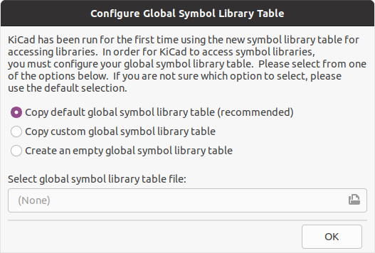
Quando l’editor degli schemi viene eseguito per la prima volta, se il file della tabella librerie di simboli globale sym-lib-table non si trova nella cartella di configurazione di KiCad, KiCad chiederà come creare questo file:
Si consiglia la prima opzione (Copia tabella libreria simboli globale predefinita (consigliato)). La tabella librerie impronte predefinita include molte delle librerie impronte standard che sono installate assieme a KiCad.
Se questa opzione è disabilitata, KiCad non è stato in grado di trovare la tabella della libreria di simboli globale predefinita. Questo probabilmente significa che non sono state installate le librerie di simboli standard con KiCad, o che non sono installate dove KiCad si aspetta di trovarle. Su alcuni sistemi le librerie KiCad sono installate come pacchetto separato.
-
Se si ha installato le librerie di simboli standard di KiCad e vuole usarle, ma la prima opzione è disabilitata, selezionare la seconda opzione e andare al file
sym-lib-tablenella cartella in cui sono state installate le librerie di KiCad. -
Se si ha già una tabella librerie di simboli personalizzata che si vorrebbe usare, selezionare la seconda opzione e cercare il proprio file
sym-lib-table. -
Se si vuole costruire una nuova tabella librerie di simboli da zero, selezionare la terza opzione.
La gestione delle librerie di simboli viene descritta in maggior dettaglio più avanti.
Interfaccia utente dell’editor degli schemi elettrici
L’interfaccia utente principale dell’editor degli schemi elettrici è mostrata sopra. Il centro contiene l’area di modifica principale, che è circondata da:
-
Barre degli strumenti principali (gestione dei file, strumenti di zoom, strumenti di modifica)
-
Barra degli strumenti di sinistra (opzioni di visualizzazione)
-
Pannello dei messaggi e barra di stato in basso
-
Pannello di destra (strumenti di disegno e progettazione)
Navigazione nell’area di lavoro
L’area di lavoro mostra lo schema in fase di progettazione. È possibile traslare la vista e fare lo zoom su diverse parti dello schema e aprire qualsiasi foglio dello schema nel progetto.
By default, dragging with the middle or right mouse button will pan the canvas view and scrolling the mouse wheel will zoom the view in or out. You can change this behavior in the Mouse and Touchpad section of the preferences (see Configuration and Customization for details).
Several other zoom tools are available in the top toolbar:
-
 zooms in on the center of the viewport.
 -
 zooms out from the center of the viewport.
 -
 zooms to fit the frame around the drawing sheet.
 -
 zooms to fit every item in the schematic (not including the drawing sheet). For instance, if there are items placed outside of the drawing sheet, they will be visible after zooming to objects.
 -
 allows you to draw a box to determine the zoomed area.
The cursor’s current position is displayed at the bottom of the window (X and Y), along with the current zoom factor (Z), the cursor’s relative position (dx, dy, and dist), the grid setting, and the display units.
Le coordinate relative possono essere azzerate premendo Spazio. È utile per effettuare misure tra due punti o per allineare oggetti.
Comandi da tastiera
The Ctrl+F1 shortcut displays the current hotkey list. The default hotkey list is included in the Actions Reference section of the manual.
The hotkeys described in this manual use the key labels that appear on a standard PC keyboard. On an Apple keyboard layout, use the Cmd key in place of Ctrl, and the Option key in place of Alt.
Molte azioni non hanno tasti comando assegnati per impostazione predefinita, ma i tasti comando possono essere assegnati o ridefiniti utilizzando l’editor di tasti comando (Preferenze → Preferenze… → Tasti comando ).
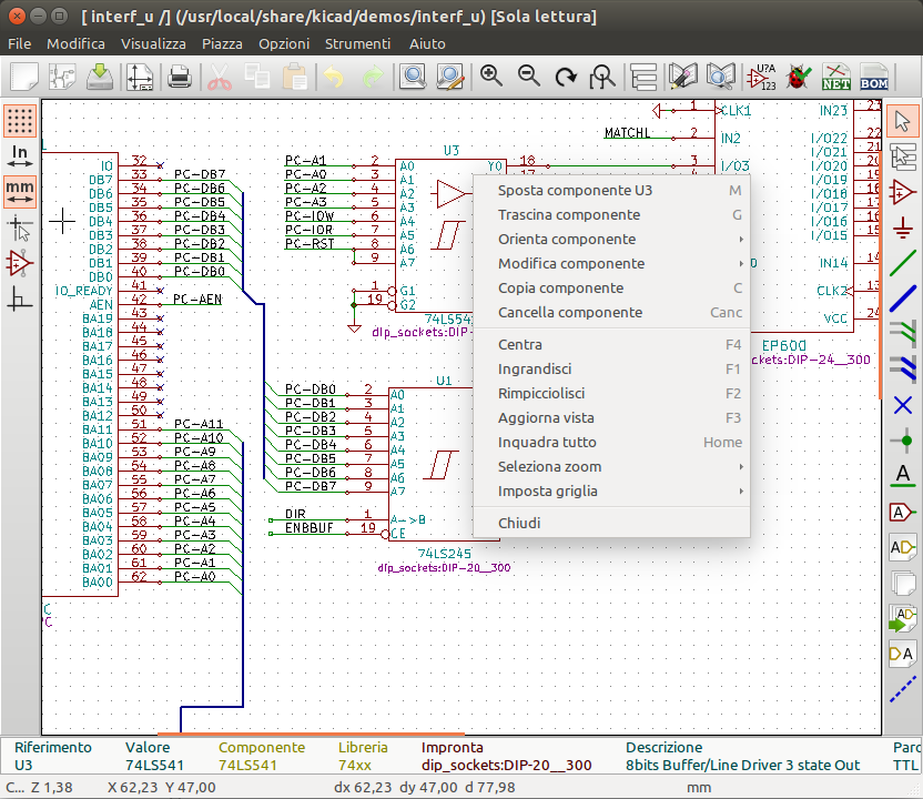
| Many of the actions available through hotkeys are also available in context menus. To access the context menu, right-click in the editing canvas. Different actions will be available depending on what is selected or what tool is active. |
I comandi da tastiera sono memorizzati nel file user.hotkeys nella cartella di configurazione di KiCad. La posizione cambia a seconda della piattaforma:
-
Windows:
%APPDATA%\kicad\7.0\user.hotkeys -
Linux:
~/.config/kicad/7.0/user.hotkeys -
macOS:
~/Library/Preferences/kicad/7.0/user.hotkeys
KiCad può importare le impostazioni dei tasti comando da un file user.hotkeys utilizzando il pulsante Importa tasti comando nell’editor di tasti comando.
Operazioni e selezione col mouse
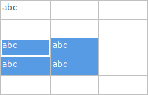
Selecting items in the editing canvas is done with the left mouse button. Single-clicking on an object will select it. Clicking and dragging will perform a box selection. A box selection from left to right will only select items that are fully inside the box. A box selection from right to left will select any items that touch the box. A left-to-right selection box is drawn in yellow, with a cursor that indicates exclusive selection, and a right-to-left selection box is drawn in blue with a cursor that indicates inclusive selection.
The selection action can be modified by holding modifier keys while clicking or dragging. The following modifier keys apply when clicking to select single items:
| Modifier Keys (Windows) | Modifier Keys (Linux) | Modifier Keys (macOS) | Selection Effect |
|---|---|---|---|
Ctrl |
Ctrl |
Cmd |
Toggle selection. |
Shift |
Shift |
Shift |
Add the item to the existing selection. |
Ctrl+Shift |
Ctrl+Shift |
Cmd+Shift |
Remove the item from the existing selection. |
long click |
long click or Alt |
long click or Option |
Clarify selection from a pop-up menu. |
The following modifier keys apply when dragging to perform a box selection:
| Modifier Keys (Windows) | Modifier Keys (Linux) | Modifier Keys (macOS) | Selection Effect |
|---|---|---|---|
Ctrl |
Ctrl |
Cmd |
Toggle selection. |
Shift |
Shift |
Shift |
Add item(s) to the existing selection. |
Ctrl+Shift |
Ctrl+Shift |
Cmd+Shift |
Remove item(s) from the existing selection. |
Selecting an object displays information about the object in the message panel at the bottom of the window. Double-clicking an object opens a window to edit the object’s properties.
Pressing Esc will always cancel the current tool or operation and return to the selection tool. Pressing Esc while the selection tool is active will clear the current selection.
Controlli di visualizzazione della barra strumenti a sinistra
La barra strumenti a sinistra fornisce le opzioni di visualizzazione degli elementi nell’editor degli schemi elettrici.
|
Turns grid display on/off. Note: by default, hiding the grid will disable grid snapping. This behavior can be changed in the Display Options section of Preferences. |
|
Display/entry of coordinates and dimensions in inches, mils, or millimeters. |
|
Switches between full-screen and small editing cursor (crosshairs). |
|
Turns invisible pin display on/off. |
|
Switches between free angle, 90 degree mode, and 45 degree mode for placement of new wires, buses, and graphical lines. |
|
Opens and closes the docked hierarchy navigator pane. |
Creazione e modifica di schemi elettrici
Introduzione
Uno schema elettrico progettato con KiCad è più di una semplice rappresentazione grafica di un dispositivo elettronico. Esso normalmente è il punto di ingresso di una catena di sviluppo che permette:
-
Il controllo di validità rispetto ad una serie di regole (Controllo Regole Elettriche (ERC)) per il rilevamento di errori e omissioni.
-
Generazione automatica della DIBA.
-
La generazione di una netlist per software di simulazione tipo SPICE.
-
Definizione di un circuito per il trasferimento delle informazioni nella progettazione del circuito stampato.
Uno schema elettrico consiste principalmente di simboli, fili, etichette, giunzioni, bus e simboli di potenza. Per chiarezza, negli schemi elettrici, è possibile inserire elementi puramente grafici come elementi bus, commenti, e polilinee.
I simboli vengono aggiunti allo schema dalle librerie di simboli. Dopo aver creato lo schema, l’insieme di connessioni e impronte viene importato nell’editor dei circuiti stampati per progettare la scheda.
Gli schemi possono essere contenuti in un unico foglio o suddivisi in più fogli. In KiCad, gli schemi a più fogli sono organizzati gerarchicamente, con un foglio principale e uno o più fogli secondari. Ogni foglio è il proprio file .kicad_sch ed è esso stesso uno schema completo di KiCad. L’utilizzo degli schemi gerarchici è descritto nel capitolo schemi gerarchici.
Operazioni di modifica degli schemi elettrici
Schematic editing tools are located in the right toolbar. When a tool is activated, it stays active until a different tool is selected or the tool is canceled with the Esc key. The selection tool is always activated when any other tool is canceled.
|
Selection tool (the default tool) |
|
Highlight a net by marking its wires and net labels with a different color. If the PCB Editor is also open then copper corresponding to the selected net will be highlighted as well. Net highlighting can be cleared by clicking with the highlight tool in an empty space, or by using the Clear Net Highlighting hotkey (~). |
|
Display the symbol selector dialog to place a new symbol. |
|
Display the power symbol selector dialog to place a new power symbol. |
|
Draw a wire. |
|
Draw a bus. |
|
Draw wire-to-bus entry points. These elements are only graphical and do not create a connection, thus they should not be used to connect wires together. |
|
Place a "no-connection" flag. These flags should be placed on symbol pins which are meant to be left unconnected. "No-connection" flags indicate to the Electrical Rule Checker that the pin is intentionally unconnected and not an error. |
|
Place a junction. This connects two crossing wires or a wire and a pin, which can sometimes be ambiguous without a junction (i.e. if a wire end or a pin is not directly connected to another wire end). |
|
Place a local label. Local labels connect items located in the same sheet. For connections between two different sheets, use global or hierarchical labels. |
|
Place a net class directive label. |
|
Place a global label. All global labels with the same name are connected, even when located on different sheets. |
|
Place a hierarchical label. Hierarchical labels are used to create a connection between a subsheet and the sheet’s parent sheet. See the Hierarchical Schematics section for more information about hierarchical labels, sheets, and pins. |
|
Place a hierarchical subsheet. You must specify the file name for this subsheet. |
|
Import a hierarchical pin from a subsheet. This command can be executed only on hierarchical subsheets. It will create hierarchical pins corresponding to hierarchical labels placed in the target subsheet. |
|
Place a text comment. |
|
Place a text box. |
|
Draw a rectangle. |
|
Draw a circle. |
|
Draw an arc. |
|
Draw lines. Note: Lines are graphical objects and are not the same as wires placed with the Wire tool. They do not connect anything. |
|
Place a bitmap image. |
|
Delete clicked items. |
Griglie
Nell’editor degli schemi il puntatore si sposta sempre sopra una griglia. La griglia può essere personalizzata:
-
La dimensione è modificabile usando il tasto destro del mouse o usando Visualizza → Proprietà griglia….
-
I colori possono essere modificati tramite la scheda Colori presente nella finestra di dialogo delle Preferenze (menu Preferenze → Opzioni generali).
-
La visibilità può essere accesa/spenta usando il pulsante corrispondente nella barra strumenti di sinistra.
La dimensione predefinita della griglia è 50 mils (0.050") o 1,27 millimetri.
Questa è la griglia raccomandata per piazzare simboli e fili in uno schema elettrico, e per piazzare piedini durante la progettazione di un simbolo nell’editor dei simboli.
| Wires connect with other wires or pins only if their ends coincide exactly. Therefore it is very important to keep symbol pins and wires aligned to the grid. It is recommended to always use a 50 mil grid when placing symbols and drawing wires because the KiCad standard symbol library and all libraries that follow its style also use a 50 mil grid. Using a grid size other than 50 mil will result in schematics without proper connectivity! |
È possibile usare anche griglie più piccole, ma queste servono solo per il testo e la grafica dei simboli e non è consigliato per posizionarvi pin e fili.
| Symbols, wires, and other elements that are not aligned to the grid can be snapped back to the grid by selecting them, right clicking, and clicking Align Elements to Grid. |
Magnetismo
Schematic elements such as symbols, wires, text, and graphic lines are snapped to the grid when moving, dragging, and drawing them. Additionally, the wire tool snaps to pins even when grid snapping is disabled. Both grid and pin snapping can be disabled while moving the mouse by using the modifier keys in the table below.
| Su tastiere Apple, usare il tasto Cmd al posto di Ctrl. |
| Modifier Key | Effect |
|---|---|
Ctrl |
Disable grid snapping. |
Shift |
Disable snapping wires to pins. |
Modifica proprietà dell’oggetto
All objects have properties that are editable in a dialog. Use the hotkey E or select Properties from the right-click context menu to edit the properties of selected item(s). You can only open the properties dialog if all the items you have selected are of the same type. To edit the properties of different types of items at one time, see the section below on bulk editing tools.
In properties dialogs, any field that contains a numeric value can also accept a basic math expression that results in a numeric value. For example, a dimension may be entered as 2 * 2mm, resulting in a value of 4mm. Basic arithmetic operators as well as parentheses for defining order of operations are supported.
Lavorare con i simboli
Piazzamento simboli
Per piazzare un simbolo nello schema elettrico si può usare il pulsante ![]() o il tasto A. Appare la finestra di dialogo Scegli simboli che consente di scegliere il simbolo da aggiungere. I simboli sono raggruppati per libreria.
o il tasto A. Appare la finestra di dialogo Scegli simboli che consente di scegliere il simbolo da aggiungere. I simboli sono raggruppati per libreria.
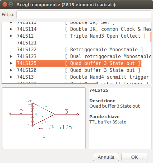
By default, only the symbol/library name and description columns are shown. Additional columns can be added by right-clicking the column header and selecting Select Columns.
La finestra di dialogo di scelta del simbolo filtrerà i simboli per nome, parolechiave, descrizione e tutti i campi simbolo aggiuntivi, a seconda di quanto si inserirà nel campo di ricerca.
Alcuni filtri avanzati sono disponibili:
-
Wildcards:
*matches any number of any characters, including none, and?matches any single character. -
Paia di chiavi-valore: se la descrizione di un componente di libreria o parola chiave contiene un marcatore nel formato "chiave:123", si può verificarne la corrispondenza relativa battendo "chiave>123" (maggiore di), "chiave<123" (minore di), ecc. I numeri possono includere uno dei seguenti suffissi indipendenti da maiuscole o minuscole:
p
n
u
m
k
meg
g
t
10-12
10-9
10-6
10-3
103
106
109
1012
ki
mi
gi
ti
210
220
230
240
-
Espressioni regolari: se si ha familiarità con le espressioni regolari, si possono usare anch’esse. Il tipo di espressione regolare usato è di stile espressione regolare avanzato dei wxWidgets, che è simile alle espressioni regolari Perl.
Se il simbolo specifica un’impronta predefinita, questa verrà visualizzata in anteprima in basso a destra. Se il simbolo include filtri impronta, è possibile selezionare impronte alternative che soddisfano i filtri impronta nel menu impronta a discesa a destra.
Dopo aver selezionato un simbolo da posizionare, il simbolo verrà attaccato al cursore. Facendo clic con il pulsante sinistro del mouse sulla posizione desiderata nello schema, il simbolo viene inserito nello schema. Prima di posizionare il simbolo nello schema elettrico, è possibile ruotarlo, renderlo speculare e modificarne i campi, usando i tasti comando o il menu contestuale del tasto destro. Queste azioni possono essere eseguite anche dopo il posizionamento.
Se l’opzione Posiziona copie ripetute è selezionata, dopo aver posizionato un simbolo, KiCad inizierà a posizionare un’altra copia del simbolo. Questo processo continua finché l’utente non preme Esc.
Per i simboli con più unità, se l’opzione Posiziona tutte le unità è selezionata, dopo aver posizionato il simbolo KiCad inizierà a posizionare l’unità successiva nel simbolo. Ciò continuerà fino a quando l’ultima unità sarà stata posizionata o sino a quando l’utente premerà Esc.
Piazzamento simboli di potenza
Un simbolo di potenza è un simbolo che rappresenta una connessione a un collegamento di potenza (N.d.T. come un’alimentazione). I simboli sono raggruppati nella libreria power, quindi possono essere posizionati utilizzando il selettore simboli. Tuttavia, poiché i posizionamenti di simboli potenza sono frequenti, è disponibile lo strumento ![]() . Questo strumento è simile, tranne per il fatto che la ricerca viene eseguita direttamente nella libreria
. Questo strumento è simile, tranne per il fatto che la ricerca viene eseguita direttamente nella libreria power e in qualsiasi altra libreria che contenga simboli di potenza.
Spostamento simboli
I simboli possono essere spostati utilizzando gli strumenti Sposta (M) o Trascina (G). Questi strumenti agiscono sul simbolo selezionato, oppure se nessun simbolo fosse stato selezionato, agiscono sul simbolo sotto il cursore.
Lo strumento Sposta sposta il simbolo stesso senza mantenere connessioni cablate ai piedini del simbolo.
Lo strumento Trascina sposta il simbolo senza interrompere le connessioni cablate ai suoi piedini, e quindi sposta anche i fili collegati.
You can also Drag symbols by clicking and dragging them with the mouse, depending on the Left button drag gesture setting in the Mouse and Touchpad section of Preferences.< Si può anche trascinare i simboli facendo clic e trascinandoli con il mouse, a seconda dell’impostazione Gesture trascinamento del pulsante sinistro nella sezione Mouse e touchpad delle Preferenze.
Symbols can also be rotated (R) or mirrored in the X (X) or Y (Y) directions.
Modifica delle proprietà del simbolo
A symbol’s fields can be edited in the symbol’s Properties window. Open the Symbol Properties window for a symbol with the E hotkey or by double-clicking on the symbol.
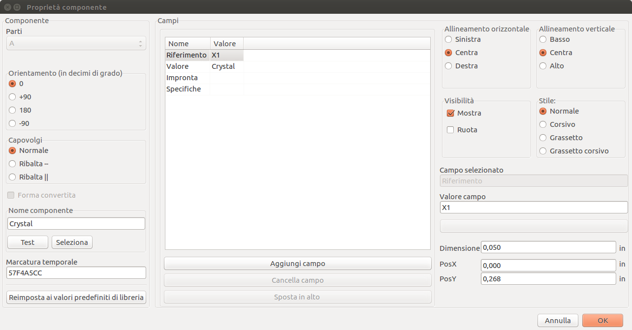
The Symbol Properties window displays all the fields of a symbol in a table. New fields can be added, and existing fields can be deleted, edited, reordered, moved, or resized.
Il nome e il valore di ciascun campo possono essere visibili o nascosti e sono disponibili diverse opzioni di formattazione: allineamento orizzontale e verticale, orientamento, posizione, carattere, colore del testo, dimensione del testo ed enfasi in grassetto/corsivo. Il posizionamento automatico del campo può anche essere abilitato in base al campo. La posizione visualizzata è sempre indicata per un simbolo visualizzato normalmente (nessuna rotazione o specularità) ed è relativa al punto di ancoraggio del simbolo.
| Le opzioni di formattazione per i campi del simbolo possono essere visualizzate o nascoste facendo clic con il pulsante destro del mouse sulla riga dell’intestazione della tabella campi simbolo abilitanto o disabilitando le colonne desiderate. Non tutte le colonne sono visibili per impostazione predefinita. |
The Update Symbol from Library… button is used to update the schematic’s copy of the symbol to match the copy in the library. The Change Symbol… button is used to swap the current symbol to a different symbol in the library. These functions are described later.
Edit Symbol… opens the Symbol Editor to edit the copy of the symbol in the schematic. Note that the original symbol in the library will not be modified. The Edit Library Symbol… button opens the Symbol Editor to edit the original symbol in the library. In this case, the symbol in the schematic will not be modified until the user clicks the Update Symbol from Library… button.
Symbols have several attributes that affect how the symbols are treated by other parts of KiCad.
Exclude from simulation prevents the symbol from being included in SPICE simulations.
Exclude from bill of materials prevents the component from being included in BOM exports.
Exclude from board means that the symbol is schematic-only, and a corresponding footprint will not be added to the PCB.
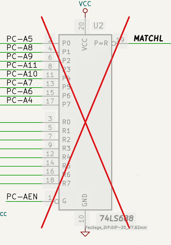
Do not populate means that the component should not be attached to the PCB, although a corresponding footprint should still be added to the board. DNP symbols appear desaturated and with a red "X" over them in the schematic, as shown below.
Modifica individuale dei campi del simbolo
An individual symbol text field can be edited directly with the E hotkey (with a field selected instead of a symbol) or by double-clicking on the field.
Some symbol fields have their own hotkey to edit them directly. With the symbol selected, the Reference, Value, and Footprint fields can be edited with the U, V, or F hotkeys, respectively.
The options in this dialog are the same as those in the full Symbol Properties dialog, but are specific to a single field.
Symbol fields can be automatically moved to an appropriate location with the Autoplace Fields action (select a symbol and press O). Field autoplacement is configurable in the Schematic Editor’s Editing Options, including a setting to always autoplace fields.
Updating and exchanging symbols
When a symbol is added to the schematic, KiCad embeds a copy of the library symbol in the schematic so that the schematic is independent of the system libraries. Symbols that have been added to the schematic are not automatically updated when the library changes. Library symbol changes are manually synced to the schematic so that the schematic does not change unexpectedly.
To update symbols in the schematic to match the corresponding symbol, use Tools → Update Symbols from Library, or right click a symbol and select Update Symbol from Library. You can also access the tool from the symbol properties dialog.
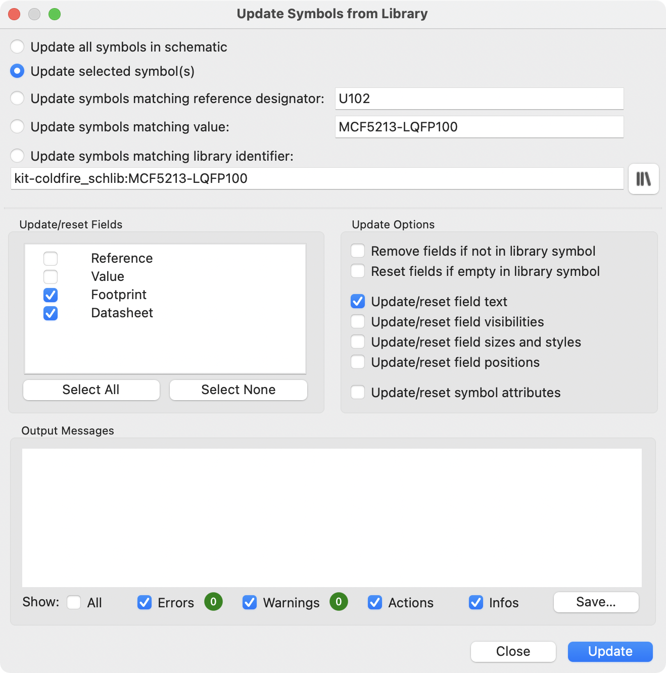
The top of the dialog has options to choose which symbols will be updated. You can update all symbols in the dialog, update only the selected symbols, or update only the symbols that match a specific reference designator, value, or library identifier. The reference designator and value fields support wildcards: * matches any number of any characters, including none, and ? matches any single character.
The middle of the dialog has options to control what parts of the symbol will be updated. You can select specific fields to update or not update, which properties of the fields to update (text, visibility, size and style, and position), and how to handle fields that are missing or empty in the library symbol. You can also choose whether to update symbol attributes, such as do not populate and exclude from simulation / bill of materials / board.
The bottom of the dialog displays messages describing the update actions that have been performed.
To change an existing symbol to a different symbol, use Edit → Change Symbols…, or right click an existing symbol and select Change Symbol…. This dialog is also accessible from the symbol properties dialog.
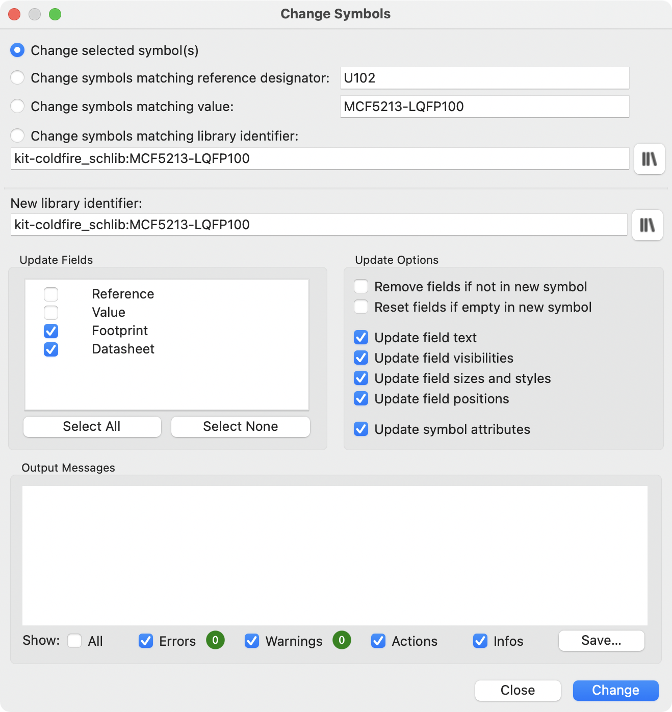
The options for the Change Symbols dialog are very similar to the Update Symbols from Library dialog.
Another way to swap existing symbols for new ones is to use Tools → Edit Symbol Library Links…. This dialog contains a table of every symbol in the design, grouped by current library symbol. By choosing a new symbol in the New Library Reference column, you can make all instances of the existing symbol instead point to the new symbol. If the Update symbol fields from new library option is used, the contents of the existing symbols' fields will be updated to match the new symbols' fields.
The Map Orphans button attempts to automatically remap orphaned symbols to symbols with the same name in an active library. For example, if there is a symbol with the current library reference mylib:symbol123, but the mylib library cannot be found, the Map Orphans button will attempt to find a symbol named symbol123 in any of the libraries that are present. This button is only enabled if orphaned symbols are present in the schematic (see the legacy schematics section).
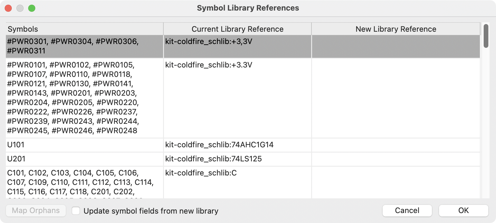
This dialog is primarily useful for managing symbols that appear in multiple libraries, when you want to switch from one library to another. For example, if a schematic uses symbols that are in both a global library and a project-specific library, the Symbol Library References dialog could be used to switch between using the global symbols or the equivalent project-specific symbols. It does not have features for fine-grained control of how fields are updated; for that, use the Change Symbols dialog.
Tabella campi del simbolo
The Symbol Fields Table allows you to view and modify field values for all symbols in a spreadsheet interface. You can open the Symbol Fields Table with the ![]() button.
button.
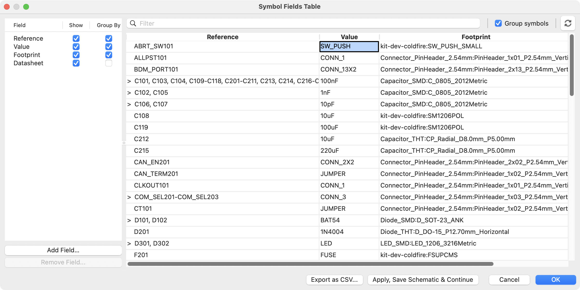
Cells are navigated with the arrow keys, or with Tab / Shift+Tab to move right / left and Enter / Shift+Enter to move down / up, respectively.
A range of cells can be selected by clicking and dragging. The whole range of selected cells will be copied (Ctrl+C) or pasted into (Ctrl+V) on a copy or paste action. Copying a range of cells from the table can be useful for creating a BOM. More details of copying and pasting cells are described below.
Any symbol field can be shown or hidden using the Show checkboxes on the left, or by right-clicking on the header of the table. New symbol fields can be added using the Add Field… button.
Similar symbols can optionally be grouped by any symbol field using the Group By checkboxes. Grouped symbols are shown in a single row in the table. The grouped row can be expanded to show the individual symbols by clicking the arrow at the left of the row. The Group Symbols checkbox enables or disables symbol grouping, and the ![]() button recalculates groupings.
button recalculates groupings.
Symbols can be filtered using the Filter textbox at the top. The filter supports wildcards: * matches any number of any characters, including none, and ? matches any single character.
You can use the Export as CSV… button to save the symbol fields to an external file. This can be used as a simple BOM generation tool, although the BOM tool provides better control over the generated output.
Trucchi per semplificare lo riempimento dei campi
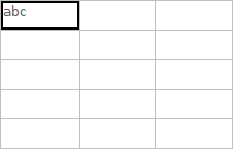
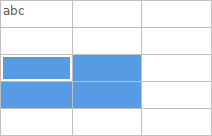
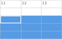
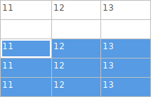
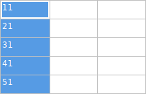
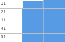
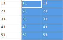
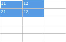
Esistono diversi metodi speciali di copia/incolla nel foglio di calcolo per incollare i valori in regioni più grandi, comprese le celle incollate con incremento automatico. Queste funzionalità possono essere utili quando si incollano valori condivisi in più simboli.
Questi metodi sono illustrati sotto.
| 1. Copia (Ctrl+C) | 2. Selezione celle obiettivo | 3. Incolla (Ctrl+V) |
|---|---|---|
|
|
|
|
|
|
|
|
|
|
|
|
|
|
|
| Queste tecniche sono disponibili anche in altre finestre di dialogo con elementi di controllo a griglia. |
Reference Designators and Symbol Annotation
Reference designators are unique identifiers for components in a design. They are often printed on a PCB and in assembly diagrams, and allow you to match symbols in a schematic to the corresponding components on a board.
In KiCad, reference designators consist of a letter indicating the type of component (R for resistor, C for capacitor, U for IC, etc.) followed by a number. If the symbol has multiple units then the reference designator will also have a trailing letter indicating the unit. Symbols that don’t have a reference designator set have a ? character instead of the number. Reference designators must be unique.
Reference designators can be automatically set when symbols are added to the schematic, and you can set or reset reference designators yourself by manually editing an individual symbol’s reference designator field or in bulk using the Annotation tool.
| The process of setting a symbol’s reference designator is called annotation. |
Auto annotazione
When auto-annotation is enabled, symbols will be automatically annotated when they are added to the schematic. You can enable auto-annotation by checking the Automatically annotate symbols checkbox in the Schematic Editor → Annotation Options pane in Preferences. Auto-annotation can also be toggled using the ![]() button in the left toolbar.
button in the left toolbar.
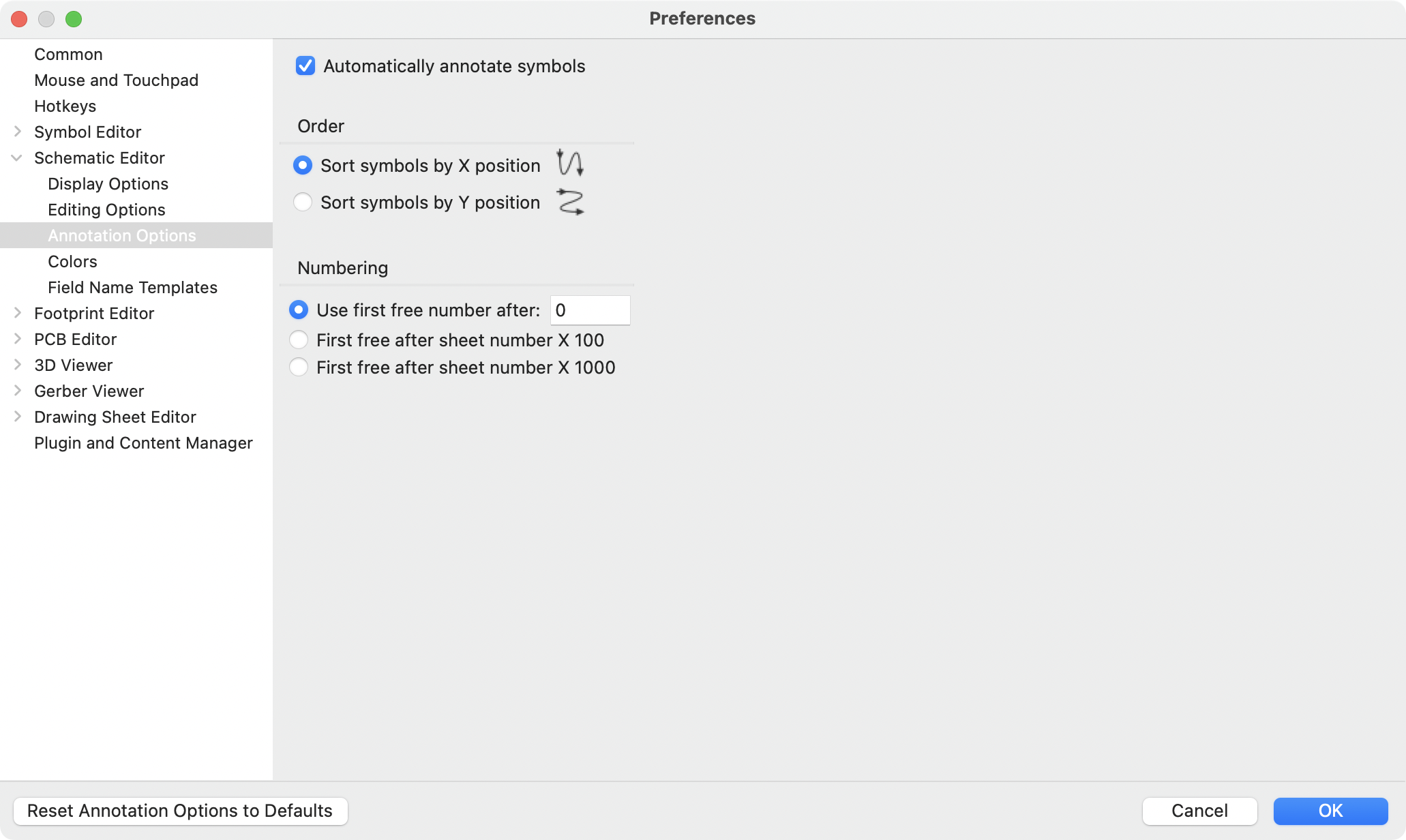
When multiple symbols are added simultaneously, they are annotated according to the Order setting, sorted by either X or Y position.
The Numbering option sets the starting number for new reference designators. This can be the lowest available number, or a number based on the sheet number.
For more information about annotation options, see the documentation for the Annotation tool.
Strumento di annotazione
Lo strumento di annotazione assegna automaticamente i riferimenti a simboli nello schema. Per eseguire lo strumento di annotazione fare clic sull’icona ![]() nella barra strumenti in alto.
nella barra strumenti in alto.
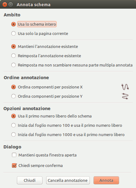
The tool provides several options to control how symbols are annotated.
Scope: Selects whether annotation is applied to the entire schematic, to only the current sheet, or to only the selected symbols. If the Recurse into subsheets option is selected, symbols in subsheets of the selected scope will be reannotated; otherwise symbols in subsheets will not be reannotated. For example, if Recurse into subsheets and Selection only selected, symbols in any selected subsheets will be reannotated.
Options: Selects whether annotation should apply to all symbols and reset *existing reference designators, or apply only to unannotated symbols.
Order: Chooses the direction of numbering. If symbols are sorted by X position, all symbols on the left side of a schematic sheet will be lower numbered than symbols on the right side of the sheet. If symbols are sorted by Y position, all symbols on the top of a sheet will be lower numbered than symbols at the bottom of the sheet.
Numbering: Selects the starting point for numbering reference designators. The lowest unused number above the starting point is picked for each reference designator. The starting point can be an arbitrary number (typically zero), or it can be the sheet number multiplied by 100 or 1000 so that each part’s reference designator corresponds to the schematic page it is on.
The Clear Annotation button clears all reference designators in the selected scope.
Annotation messages can be filtered with the checkboxes at the bottom or saved to a report using the Save… button.
Connessioni elettriche
There are two primary ways to establish connections: wires and labels. Wires make direct connections, while labels connect to other labels with the same name. Both wires and labels are shown in the schematic below.
Connections can also be made with buses and with implicit connections via hidden power pins.
This section will also discuss two special types of symbols that can be added with the "Power symbol" button on the right toolbar:
-
Simboli di potenza: simboli per connettere una linea di potenza o di massa.
-
PWR_FLAG: a specific symbol for indicating that a net is powered when it is not connected to a power output pin (for example, a power net that is supplied by an off-board connector).
Fili
I fili vengono utilizzati per stabilire direttamente collegamenti elettrici tra due punti. Per stabilire una connessione, un segmento di filo deve essere collegato per la sua estremità a un altro segmento o ad un pin. Solo le estremità dei fili creano connessioni; se un filo attraversa il centro di un altro filo, non verrà effettuata una connessione.
Unconnected wire ends have a small square that indicates the connection point. The square disappears when a connection is made to the wire end. Unconnected pins have a circle, which also disappears when a connection is made.
| Wires connect with other wires or pins only if their ends coincide exactly. Therefore it is important to keep symbol pins and wires aligned to the grid. It is recommended to always use a 50 mil grid when placing symbols and drawing wires because the KiCad standard symbol library and all libraries that follow its style also use a 50 mil grid. |
| Symbols, wires, and other elements that are not aligned to the grid can be snapped back to the grid by selecting them, right clicking, and selecting Align Elements to Grid. |
Disegno e modifica fili
To begin connecting elements with wire, use the Wire tool ![]() in the right toolbar (w). Wires can also be automatically started by clicking on an unconnected symbol pin or wire end.
in the right toolbar (w). Wires can also be automatically started by clicking on an unconnected symbol pin or wire end.
You can restrict wires to 90 degree angles using the ![]() button in the left toolbar, or to 45 degree angles with the
button in the left toolbar, or to 45 degree angles with the ![]() button. The
button. The ![]() button allows you to place wires at any angle. You can cycle through these modes using Shift+Space, or select the desired mode in Preferences → Schematic Editor → Editing Options. These modes affect graphic lines in addition to wires.
button allows you to place wires at any angle. You can cycle through these modes using Shift+Space, or select the desired mode in Preferences → Schematic Editor → Editing Options. These modes affect graphic lines in addition to wires.
As in the PCB editor, the / hotkey switches wire posture.
Wires can be moved and edited using the Move (M) or Drag (G) tools. As with symbols, the Move tool moves only the selected segment, without maintaining existing connections to other segments. The Drag tool maintains existing connections.
You can select connected wires using the Select Connection tool (Alt+4). This tool selects all connected wire segments until it reaches a junction, starting with the selected segment or the segment under the cursor. Using the tool again expands the existing selection to the next junction.
You can break a wire segment into two pieces by right-clicking a wire and selecting Slice. The segment will be separated at the current mouse position. You can also separate a wire segment from the adjacent segments by right-clicking the segment and selecting Break.
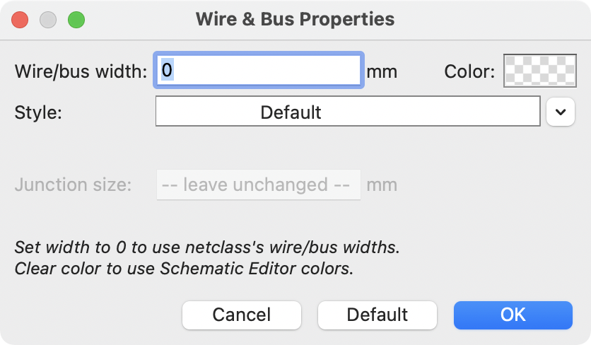
Normally the line style of a wire follows the net’s netclass settings (nets are in the Default netclass if no other netclass is specified). However, the line style for the selected wire segments can be overridden in the wire’s properties dialog (E when a wire segment is selected). The wire’s width, color, and line style (solid, dashed, dotted, etc.) can be set. Setting the width to 0, clearing the color, and using the Default line style uses the default width, color, and style, respectively, from the netclass settings. If a wire junction is included in the selection, the junction size can also be edited here.
Giunzioni di fili
I fili che si incrociano non sono implicitamente connessi. È necessario collegarli assieme esplicitamente con un punto di giunzione se si vuole stabilire una connessione (pulsante ![]() nella barra strumenti a destra). I punti di giunzione verranno aggiunti automaticamente ai fili che cominciano o finiscono su altri fili esistenti.
nella barra strumenti a destra). I punti di giunzione verranno aggiunti automaticamente ai fili che cominciano o finiscono su altri fili esistenti.
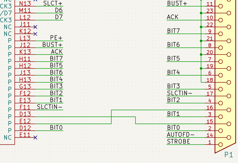
I punti di giunzione sono utilizzati nella figura dello schema precedente sui fili collegati ai pin 18, 19, 20, 21, 22 e 23 di P1.
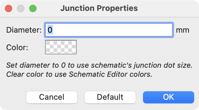
Junction size automatically follows the schematic’s Junction dot size setting in Schematic Setup → General → Formatting. Color follows the netclass setting. The automatic size and color can be overridden in each junction dot’s properties; a size of 0 is equivalent to the schematic default size, and clearing the color uses the netclass color.
Etichette
Labels are used to assign net names to wires and pins. Wires with the same net name are considered to be connected, so labels can be used to make connections without drawing direct wire connections.
Una net può avere un solo nome. Se due etichette diverse vengono posizionate sulla stessa rete, verrà generata una violazione ERC. Nella netlist verrà utilizzato solo uno dei nomi di net. Il nome della net finale è determinato in base alle regole descritte di seguito.
There are three types of labels, each with a different connection scope.
-
Local labels, also referred to simply as labels, only make connections within a sheet. Add a local label with the
 button in the right
toolbar.
button in the right
toolbar. -
Global labels make connections anywhere in a schematic, regardless of sheet. Add a global label with the
 button in the right
toolbar.
button in the right
toolbar. -
Hierarchical labels connect to hierarchical sheet pins and are used in hierarchical schematics for connecting child sheets to their parent sheet. Add a hierarchical label with the
 button in the right toolbar.
| Labels that have the same name will connect, regardless of the label type, if they are in the same sheet. |
Aggiunta e modifica etichette
After using the appropriate button or hotkey to create a label, the Label Properties dialog appears.
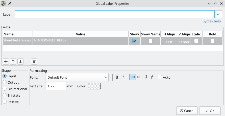
The Label field sets the label’s text, which determines the net that the label assigns to its attached wire. Label text supports markup for overbars, subscripts, etc., as well as variable substitution. Use the Syntax help link in the dialog for a summary.
There are several options to control the label’s appearance. You can change the font, size, and color of the text, and set bold and italic emphasis. You can also set the orientation of the text relative to the label’s connection point. Hierarchical and global labels have several additional options: the Auto option automatically sets the label orientation based on the connected schematic elements, and Shape option controls the shape of the label outline (Input, Output, Bidirectional, Tri-state, or Passive). The outline shape is purely visual and has no electrical consequence.
| The default text size can be set for a schematic in Schematic Setup, and the default font can be set in Preferences. |
| Global labels have additional settings to control margins around the label text in the Schematic Setup dialog. |
Labels can also have fields added to them. Two fields have special meaning (Net Class and Sheet References, described below), but arbitrary fields can also be added. Label fields behave like symbol fields: you can show or hide their name and value and adjust the alignment, orientation, position, size, font, color, and emphasis.
| Le opzioni di formattazione per i campi etichetta possono essere visualizzate o nascoste facendo clic con il pulsante destro del mouse sulla riga dell’intestazione della tabella campi etichetta e abilitando o disabilitando le colonne desiderate. Non tutte le colonne sono visibili per impostazione predefinita. |
Like symbol fields, label fields can be edited individually by opening the properties of a specific label field from the schematic (double click the label field, or use E).
After accepting the label properties, the label is attached to the cursor for placement. The connection point for a label is the small square in the corner of the label. The square disappears when the label is connected to a wire or the end of a pin.

The connection point’s position relative to the label text can be changed by choosing a different label orientation in the label’s properties, or by mirroring/rotating the label.
The Label Properties dialog can be accessed at any time by selecting a label and using the E hotkey, double-clicking on the label, or with Properties… in the right-click context menu.
Assigning net classes with labels
In addition to assigning net names, labels can be used to assign net classes. A label field named Net Class assigns the specified netclass to the net associated with the label. To make it easier to assign net classes in this way, Net Class is the default name for new label fields, and Net Class fields present a dropdown list of all the net classes in the design. Net classes must be created in the Schematic Setup or Board Setup windows before they can be assigned with a label field.
For more information about assigning netclasses, see the netclass documentation.
Inter-sheet references
Global labels can display inter-sheet references, which are a list of page numbers for other places in the schematic where the same global label appears. Clicking an inter-sheet reference travels to the listed page. If multiple references are listed, clicking the reference list brings up a menu to select the desired page.
Inter-sheet references are globally controlled in the Schematic Setup window’s Formatting page. References can be enabled or disabled, and the displayed format for the list can be adjusted, including with optional prefix or suffix characters.
The image below shows a global label with inter-sheet references to two other schematic pages. A prefix and suffix of [ and ], respectively, were added in Schematic Setup.
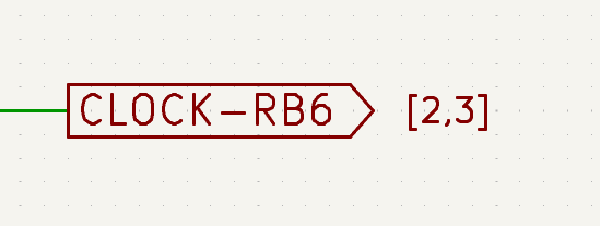
A Sheet References field with value ${INTERSHEET_REFS} is automatically added to global labels, and is used to control the appearance of inter-sheet references for that label. The ${INTERSHEET_REFS} text variable gets expanded to the full list of inter-sheet references for the global label, as configured in Schematic Setup. Visibility of inter-sheet references is globally controlled in Schematic Setup rather than with the Sheet References field visibility control. The Sheet References field has no meaning for other types of labels.
Buses
I bus sono un modo per raggruppare segnali in relazione tra loro in uno schema elettrico, in modo da semplificare i progetti complessi. I bus possono essere disegnati come i fili usando lo strumento bus ![]() , e i loro nomi vengono assegnati usando le etichette allo stesso modo di come si fa con i fili dei segnali.
, e i loro nomi vengono assegnati usando le etichette allo stesso modo di come si fa con i fili dei segnali.
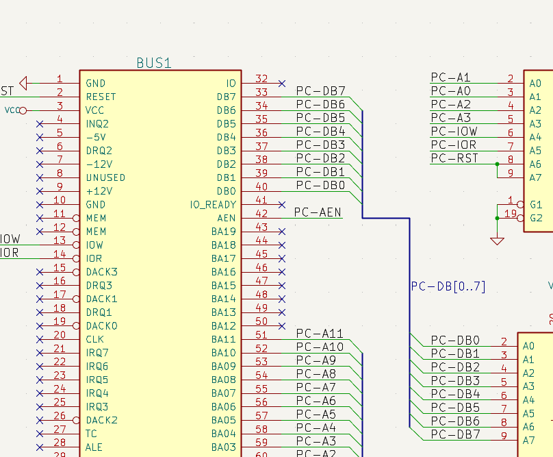
Nello schema elettrico seguente, molti piedini sono connessi a dei bus, cioè le linee spesse blu al centro.
Membri di bus
There are two types of bus in KiCad 6.0 and later: vector buses and group buses.
Un bus vettoriale è un insieme di segnali che cominciano con un prefisso comune e finiscono con un numero. I bus vettoriali hanno nome nella forma <PREFISSO>[M..N] dove PREFISSO è un qualsiasi nome di segnale valido, M è il primo numero del suffisso, e N è l’ultimo numero del suffisso. Per esempio, il bus DATA[0..7] contiene i segnali DATA0, DATA1, e così via fino a DATA7. Non importa in quale ordine M ed N vengono specificati, ma entrambi devono essere positivi.
Un bus di gruppo è un insieme di uno o più segnali e/o bus vettoriali. I bus di gruppo possono essere usati per tenere assieme segnali correlati anche quando questi hanno nomi diversi. I bus di gruppo usano una sintassi etichetta speciale:
<NOME_OPZIONALE>{SEGNALE1 SEGNALE2 SEGNALE3}
I membri del gruppo sono elencati dentro parentesi graffe ({}) separati da spazi. Il nome opzionale del gruppo va prima della prima parentesi. Se il bus di gruppo è anonimo, i collegamenti risultanti sul C.S. saranno semplicemente i nomi dei segnali dentro il gruppo. Se il bus di gruppo possiede un nome, i collegamenti risultanti avranno il nome come prefisso, con un punto (.) di separazione tra il prefisso e il nome del segnale.
Per esempio, il bus {SCL SDA} ha due segnali membri, e nella netlist questi segnali saranno SCL e SDA. Il bus USB1{DP DM} genererà collegamenti chiamati USB1.DP e USB1.DM. Per progetti con bus grandi, ripetuti tra diversi circuiti simili, l’uso di questa tecnica può far risparmiare tempo.
I bus di gruppo possono contenere anche bus vettoriali. Per esempio, il bus MEMORY{A[7..0] D[7..0] OE WE} contiene sia bus vettoriali che segnali normali, il ché porterà a del collegamenti del tipo MEMORY.A7 e MEMORY.OE sul C. S. .
I fili di bus si possono disegnare e collegare allo stesso modo dei fili dei segnali, compreso l’uso di giunzioni per creare connessioni tra fili che si incrociano. Come per i segnali, i bus non possono avere più di un nome — se due etichette in conflitto sono associate allo stesso bus, verrà generato un errore di controllo regole elettriche (ERC).
Connessioni tra membri di bus
Piedini connessi tra gli stessi membri di un bus devono essere connessi da etichette. Non è possibile connettere un piedino direttamente ad un bus; questo tipo di connessione sarà ignorata da KiCad.
Nell’esempio sopra, le connessioni vengono effettuate dalle etichette piazzate sui fili connessi ai piedini. Le voci di bus (segmenti di filo a 45 gradi) sono solo elementi grafici, e non sono necessarie per formare connessioni logiche.
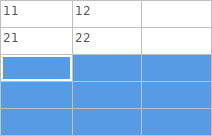
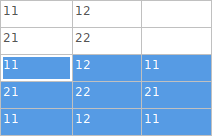
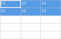
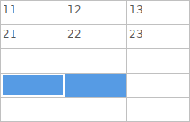
In effetti, usando il comando di ripetizione (Ins), le connessioni possono essere eseguite molto velocemente nel modo seguente, se i piedini del componente sono allineati in ordine incrementale (una pratica comune in componenti come memorie, microprocessori, ecc.):
-
Piazzare la prima etichetta (per esempio
PCA0) -
Usare il tasto di ripetizione quanto serve per piazzare membri. KiCad creerà automaticamente le etichette successive (
PCA1,PCA2…) allineate verticalmente, teoricamente nella esatta posizione degli altri piedini. -
Disegnare il filo sotto la prima etichetta. Usare poi il comando di ripetizione per piazzare gli altri fili sotto le etichette.
-
Se necessario, piazzare le voci di bus allo stesso modo (piazzare la prima voce, poi usare il tasto di ripetizione).
|
Nella sezione Editor schemi elettrici → Opzioni di modifica del menu delle preferenze, è possibile impostare i parametri di ripetizione:
|
Dispiegamento bus
Lo strumento di dispiegamento permette di estrarre velocemente i segnali da un bus. Per dispiegare un segnale, fare clic con il tasto destro del mouse su un oggetto di tipo bus (un filo di bus, ecc) e scegliere Dispiega bus. In alternativa, usare il tasto comando Dispiega bus (predeinito:C) quando il puntatore è posizionato sopra un oggetto di tipo bus. Il menu permette di selezionare quale membro del bus dispiegare.
Dopo aver selezionato il membro del bus, il successivo clic posizionerà l’etichetta del membro del bus alla posizione desiderata. Lo strumento genera automaticamente una voce bus ed un filo in direzione della posizione dell’etichetta. Dopo il posizionamento dell’etichetta, si può continuare a posizionare altri segmenti di filo (per esempio, per connetterli ai pin di un componente) e completare il collegamento in uno qualsiasi dei normali metodi.
Alias di bus
Gli alias di bus sono scorciatoie che permettono di lavorare con grandi insiemi di bus in modo più efficiente. Essi permettono di definire un gruppo di bus e dare ad esso un nome corto che può essere usato poi al posto del nome completo in tutto lo schema elettrico.
To create bus aliases, open the Bus Alias Definitions pane in Schematic Setup.
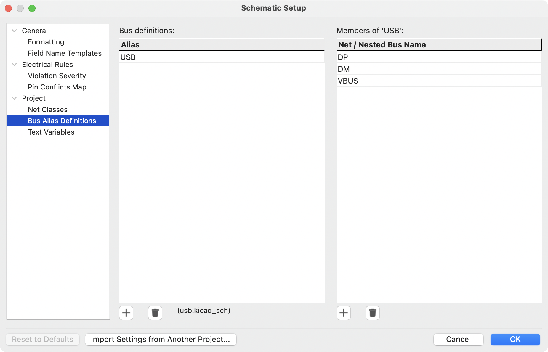
Ad un alias si può dare come nome un qualsiasi nome di segnale valido. Usando la finestra di dialogo, si possono aggiungere segnali o bus vettoriali all’alias. Come scorciatoia, si può battere o incollare dentro un’elenco di segnali e/o buse separati da spazi, e questi verranno aggiunti alla definizione di alias. In questo esempio, definiamo un alias chiamato USB con membri DP, DM, e VBUS.
Dopo la definizione di un alias, esso può essere usato in una etichetta di bus di gruppo mettendo il nome dell’alias dentro le parentesi graffe del bus di gruppo: {USB}. Ciò ha lo stesso effetto dell’etichettare il bus {DP DM VBUS}. Si può anche aggiungere un nome prefisso al gruppo, come USB1{USB}, il che da come risultati collegamenti come USB1.DP come descritto sopra. Per bus complessi, l’uso di alias può rendere l’etichettatura dello schema elettrico molto più corta. Si faccia attenzione al fatto che gli alias sono solo scorciatoie, e che il nome dell’alias non viene incluso nella netlist.
Bus aliases are saved in the schematic file that is opened when the alias is created. The Bus Alias Definitions window shows the schematic file associated with the selected alias at the bottom of the alias list. Any aliases created in a given schematic sheet are available to use in any other schematic sheet that is in the same hierarchical design. If multiple sheets in a hierarchical design contain identically-named bus aliases, the aliases must all have the same members. ERC will report a violation if multiple bus aliases with the same name do not have consistent members.
Bus con più di una etichetta
KiCad 5.0 e versioni precedenti permettevano la connessione di bus con diverse etichette assieme, e collegavano assieme i membri di detti bus durante la creazione della netlist. Questo comportamento è stato eliminato in KiCad 6.0 perché è incompatibile con i bus di gruppo, e anche perché tendeva a creare confusione nelle netlist perché il nome che un dato segnale avrebbe ricevuto non era facilmente predicibile.
Se si apre un progetto che faceva uso di questa caratteristica in una versione moderna di KiCad, si potrà osservare la finestra di dialogo di ``Migrazione bus'' che vi guiderà attraverso la procedura di aggiornamento dello schema in modo tale da garantire l’esistenza di una sola etichetta per un dato insieme di collegamenti bus.
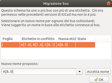
Per ogni insieme di fili di bus che ha più di una etichetta, è necessario scegliere l’etichetta da tenere. Il menu a discesa permette di scegliere tra le etichette che esistono nel progetto, oppure è anche possibile scegliere un nome ancora diverso inserendolo manualmente nel campo del nuovo nome.
Hidden Power Pins
When the power pins of a symbol are visible, they must be connected, as with any other signal. However, symbols such as gates and flip-flops are sometimes drawn with hidden power input pins which are connected implicitly.
KiCad automatically connects invisible pins with type "power input" to a global net with the same name as the pin. For example, if a symbol has a hidden power input pin named VCC, this pin will be globally connected to the VCC net on all sheets.
|
Hidden pins can be shown in the schematic by checking the Show hidden
pins option in the Schematic Editor → Display Options section
of the preferences, or by selecting View → Show hidden pins.
There is also a toggle icon |
It may be necessary to join power nets of different names (for example, GND in TTL components and VSS in MOS components). To accomplish this, add a power symbol for each net and connect them with a wire.
Se vengono usati pin di potenza nascosti, non è raccomandabile usare etichette locali per le connessioni di potenza, dato che queste ultime non connetterebbero i piedini di potenza nascosti su altri fogli.
| Care must be taken with hidden power input pins because they can create unintentional connections. By nature, hidden pins are invisible and do not display their pin name. This makes it easy to accidentally connect two power pins to the same net. For this reason, using invisible power pins in symbols is not recommended outside of power symbols, and is only supported for compatibility with legacy designs and symbols. |
Power Symbols
Power symbols are symbols that are conventionally used to represent a connection to a power net, such as VCC or GND. In addition to being a visual indicator that the attached net is a power rail, power symbols make global connections: two power symbols with the same pin name connect to each other anywhere in the schematic, regardless of sheet.
Power symbols are virtual: they do not represent a physical component on the PCB.
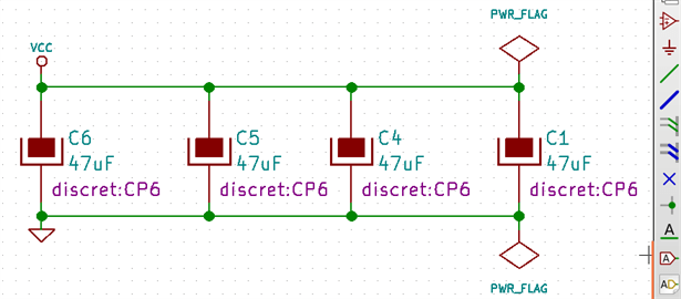
In the figure below, power symbols are used to connect the positive and negative terminals of the capacitors to the VCC and GND nets, respectively.
In the KiCad standard library, power symbols are found in the power library, but power symbols can be created in any library.
To create a custom power symbol, make a new symbol with a power input pin that is set to be invisible. Name the pin according to the desired power net. In addition, set the "Define as power symbol" symbol property. As described in the hidden power pins section, invisible power input pins make global connections based on the hidden power pin’s name. The process of creating a power symbol is described in more detail in the Symbol Editor section.
| The connected net name is determined by the power symbol’s pin name, not the name or value of the symbol. This means that power symbol net names can only be changed in the symbol editor, not in the schematic. |
Net name assignment rules
Every net in the schematic is assigned a name, whether that name is specified by the user or automatically generated by KiCad.
When multiple labels are attached to the same net, the final net name is determined in the following order, from highest priority to lowest:
-
Etichette globali
-
Etichette locali
-
Etichette gerarchiche
-
Pin fogli gerarchici
If there are multiple labels of one type attached to a net, the names are sorted alphabetically and the first is used.
If a net travels through multiple sheets of a hierarchy, it will take its name from the highest level of the hierarchy where it has a hierarchical label or local label. As usual, local labels take priority over hierarchical labels.
If none of the label types above are attached to a net, the net’s name is automatically generated based on the connected symbol pins.
PWR_FLAG
Due simboli PWR_FLAG sono visibili nella schermata soprastante. Essi indicano all’ERC che le due net di potenza VCC e GND sono effettivamente connesse ad una sorgente di potenza, dato che non c’è una sorgente di potenza esplicita come l’uscita di un regolatore di tensione collegata a nessuno dei due collegamenti.
Without these two flags, the ERC tool would diagnose: Error: Input Power pin not driven by any Output Power pins.
The PWR_FLAG symbol is found in the power symbol library. The same effect can be achieved by connecting any power output pin to the net.
Indicatore di Non-connesso
No-connection flags (![]() ) are used to indicate that a pin is intentionally unconnected. These flags prevent "unconnected pin" ERC warnings for pins that are intentionally unconnected.
) are used to indicate that a pin is intentionally unconnected. These flags prevent "unconnected pin" ERC warnings for pins that are intentionally unconnected.
Note that no-connection flags are distinct from the "unconnected" symbol pin type, although they both prevent "unconnected pin" ERC warnings on the pin in question.
Netclasses
Netclasses are groups of nets that can be assigned design rules (for the PCB) and graphical properties (for the schematic). In KiCad, each net is part of exactly one net class. If you do not add a net to a specific class, it will be part of the Default class, which always exists.
Net classes may be created and edited in either the Schematic or Board Setup dialogs. Nets can be added to netclasses in either the schematic or board using pattern-based assignments described below. Nets can also be assigned to netclasses in the schematic using graphical assignments with net class directives or net labels.
Selecting a wire or label displays the net’s netclass in the message panel at the bottom of the window.
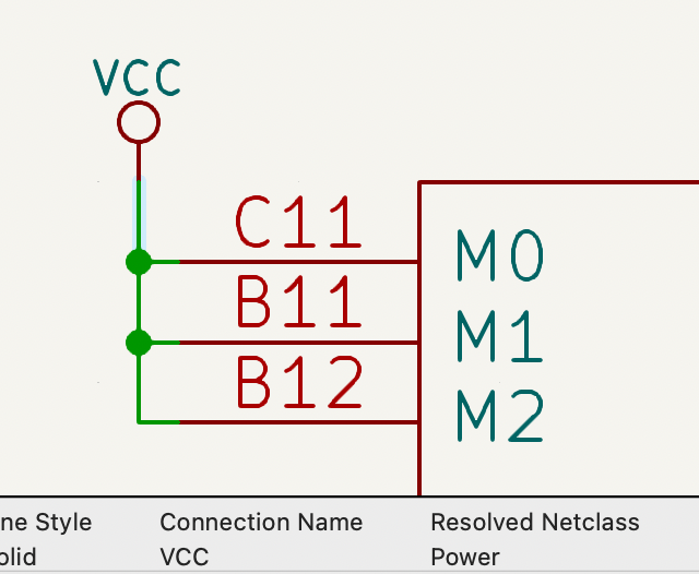
Managing netclasses in Schematic Setup
Netclasses are managed in the Net Classes panel of the Schematic Setup dialog.
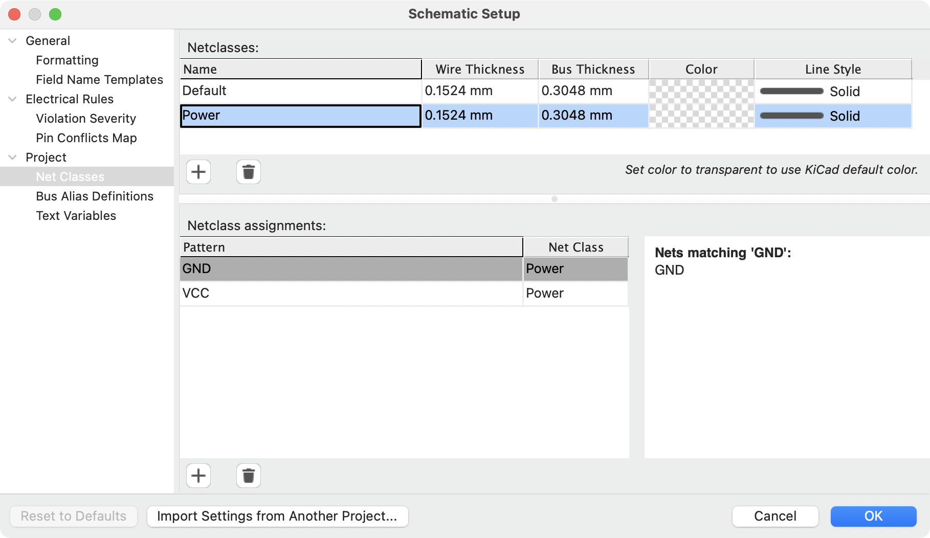
The top pane lists the netclasses that exist in the design. The Default netclass always exists, and you can add additional netclasses with the ![]() button or remove the selected netclass with the
button or remove the selected netclass with the ![]() button.
button.
Each netclass can have unique graphic properties that determine how wires of that netclass are displayed in the schematic. Wire and bus thicknesses, color, and line style (solid, dashed, dotted, etc.) can all be adjusted. Setting the color to transparent will use the theme’s default wire/bus color for the netclass, which is configurable in Preferences.
You can also set board design rules for each netclass, although the DRC fields are hidden by default. Right click the header row to show or hide additional columns. For more information about setting netclass design rules, see the PCB editor documentation.
The bottom pane lists pattern-based netclass assignments. Each row has a net name pattern and a netclass; nets with names that match the pattern are assigned to the specified netclass. If a net matches multiple patterns, the first match is used. Pattern-based netclass assignments are dynamic: when a new net is added that matches an existing pattern, it will be assigned to the associated netclass automatically. Net patterns can use both wildcards (* to match any number of any characters, including none, and ? to match any character) and regular expressions. The nets that match the selected pattern are displayed to the right of the pattern list.
For example, the net* pattern matches nets named net, net1, network, and any other net name beginning with net. Because * has a slightly different meaning in a regular expression (* matches zero or more of the preceding character), the net* pattern would also match a net named ne.
Remember that net names must include the full sheet path. For example, a
locally labeled net in the root sheet has a name prefixed with /.
|
Use the ![]() button to add a net class assignment pattern or the
button to add a net class assignment pattern or the ![]() button to remove a pattern.
button to remove a pattern.
A netclass pattern containing only the * wildcard will match all
explicitly named nets, but will not match unlabeled nets. To match
unlabeled nets, you can include more of the net name before the wildcard
character. All unlabeled nets have names that begin with Net-, so the
pattern Net-* will match all unlabeled nets. You can also assign a
netclass to an unlabeled net using a
net class directive.
|
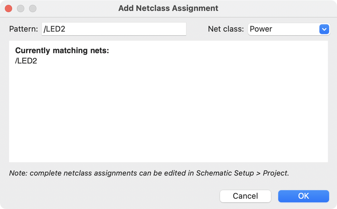
Instead of adding netclass patterns in the Schematic Setup dialog, you can directly create netclass patterns from the schematic canvas. Right click a net and select Assign Netclass… to bring up the Add Netclass Assignment dialog. The netclass pattern is pre-filled with the name of the selected net, but the pattern can be changed if desired. All nets matching the pattern are displayed in the dialog.
Graphically assigning netclasses in the schematic
As an alternative to pattern-based netclass assignment, netclasses can be graphically assigned to nets in the schematic using either net class directives or labels. Netclasses must be created in Schematic Setup before they can be assigned graphically.
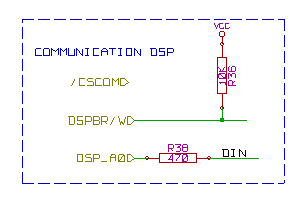
In the image below, a net class directive is used to assign signals to the 50R netclass.
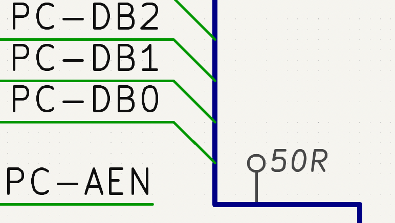
Net class directives are added with the ![]() button in the right toolbar. They behave like labels, except that they cannot be used to name a net. The attached net is assigned a netclass according to the value of the directive’s
button in the right toolbar. They behave like labels, except that they cannot be used to name a net. The attached net is assigned a netclass according to the value of the directive’s Net Class field. The Net Class field presents a dropdown list of all the net classes in the design.
If a directive is attached to a bus, all members of the bus are assigned to the specified net class.
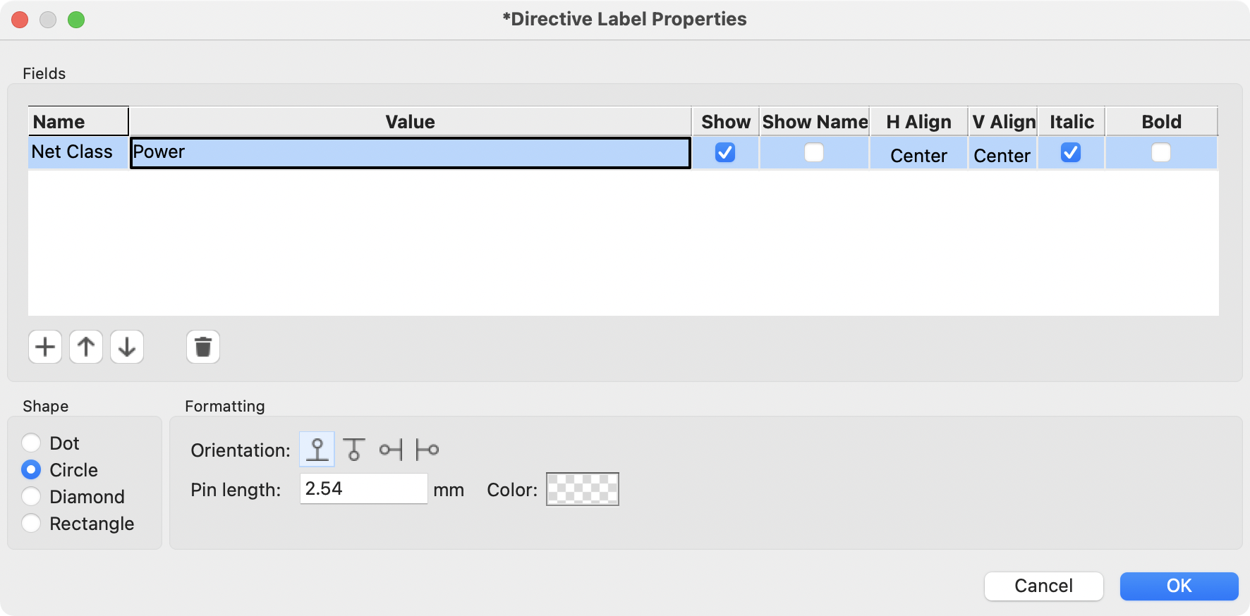
In addition to the associated netclass, you can edit the directive’s shape (dot, circle, diamond, or rectangle), orientation, pin length, and color in the directive’s properties.
Net labels can also be used to assign netclasses to nets by adding a Net Class field to the label.
If more than one different netclass is graphically assigned to a single net, ERC will report an issue. Graphical netclass assignments override pattern-based assignments: if a net matches a netclass pattern assignment and also has a netclass assigned graphically, the graphically assigned netclass will be used.
Elementi grafici
Text, graphic shapes, and images can be added to schematics for documentation purposes. These items do not have any electrical effect on the schematic.
The image below shows graphic lines and text ("COMMUNICATION DSP") in addition to symbols and several types of labels.
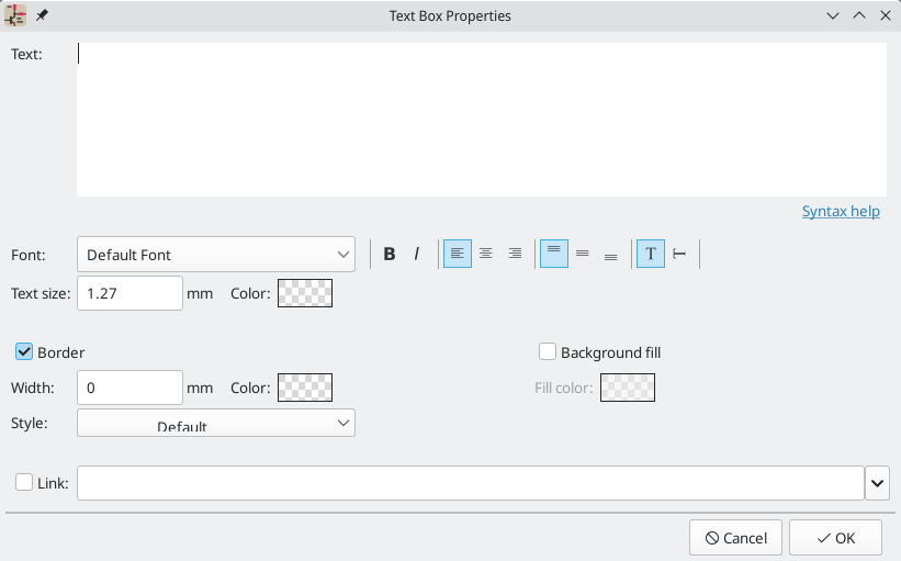
Text and Text Boxes
Two kinds of text can be added to schematics, which are referred to as text (![]() ) and text boxes (
) and text boxes (![]() ). Both are added using their respective buttons in the right toolbar.
). Both are added using their respective buttons in the right toolbar.
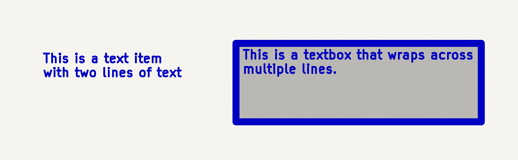
Both kinds of text item support multiline text and basic formatting features, but text boxes wrap text to fit in the outline and have additional formatting options. All text has adjustable fonts, color, size, bold and italic emphasis, left and right alignment, and vertical and horizontal orientation. Text boxes additionally support horizontal centering, vertical alignment options, and colored borders and fill.
| The default text size can be set for a schematic in Schematic Setup, and the default font can be set in Preferences. |
Links
Text and text boxes can be made into a link by entering a target in the Link box in the text properties. The link target can be a local file (using the file:// protocol prefix followed by the file’s path), to a website (using http:// or https:// followed by the rest of the URL), or to another page in the same schematic (using # followed by the page number). These can also be autofilled using the dropdown menu in the link target box.
Fonts
Text and text boxes support custom fonts, which are selectable with the Font dropdown in the properties dialog for the text. In addition to the KiCad font, you can use any TTF font installed on your computer.
| User fonts are not embedded in the project. If the project is opened on another computer that does not have the selected font installed, a different font will be substituted. For maximum compatibility, use the KiCad font. |
Text Markup
Text supports markup for superscripts, subscripts, overbars, evaluating project variables, and accessing symbol field values.
| Feature | Markup Syntax | Result |
|---|---|---|
Superscript |
|
textsuperscript |
Subscript |
|
textsubscript |
Overbar |
|
text |
|
variable_value |
|
|
field_value of symbol refdes |
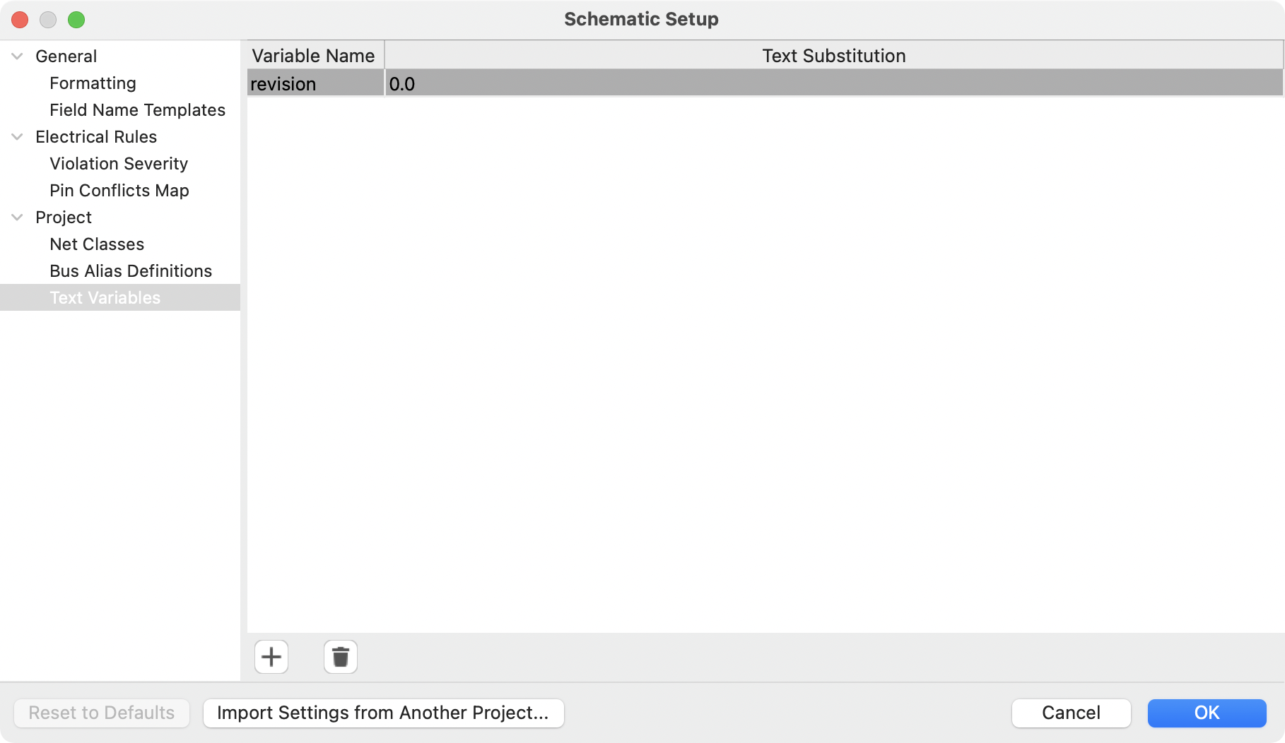
| Variables must be defined in Schematic Setup before they can be used. There are also a number of built-in system text variables. |
Graphic Shapes
Graphic rectangles (![]() ), circles (
), circles (![]() ), arcs (
), arcs (![]() ), and lines (
), and lines (![]() ) can all be added using their respective buttons in the right toolbar.
) can all be added using their respective buttons in the right toolbar.
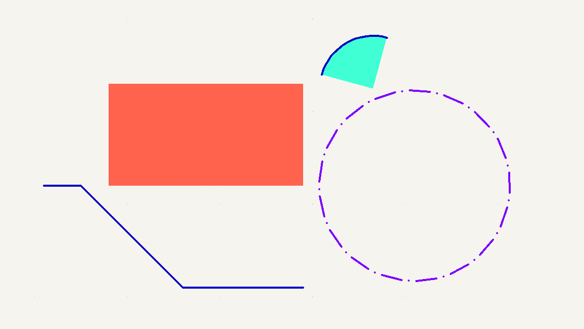
Line width, color, and style (solid, dashed, or dotted) can be configured in the properties dialog for each shape (E). Rectangles, circles, and arcs can also have a fill color set and have their outlines removed.
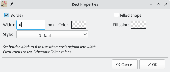
Setting a shape’s line width to 0 uses the schematic default line width, which is configurable in Schematic Setup. Spacing for line dashes is also configurable there. Removing a line or fill color uses the color theme’s graphics color, which is configurable in Preferences.
Like wires, graphic lines obey the line drawing mode setting (90 degree, 45 degree, or free angle), which you can set using the toggle buttons on the left toolbar (![]() ,
, ![]() , and
, and ![]() , respectively). Shift+Space cycles through the modes.
, respectively). Shift+Space cycles through the modes.
As with PCB tracks, the / hotkey switches line posture.
Bitmap Images
Bitmap images can be added to the schematic with the ![]() button. Images in the schematic can be moved and scaled. The properties dialog allows setting a location and scale as well as converting the image to greyscale.
button. Images in the schematic can be moved and scaled. The properties dialog allows setting a location and scale as well as converting the image to greyscale.
Bulk editing text and graphics
Properties of text and graphics can be edited in bulk using the Edit Text and Graphic Properties dialog (Tools → Edit Text and Graphic Properties…). The tool can also modify visual properties of wires and buses.
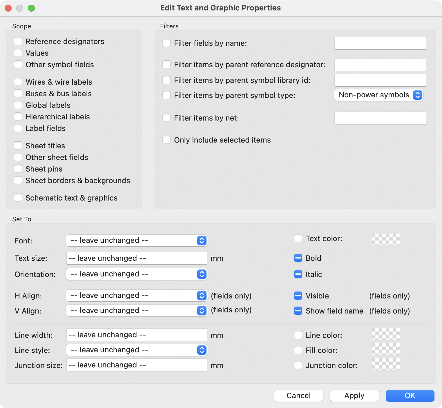
Scope and Filters
Scope settings restrict the tool to editing only certain types of objects. If no scopes are selected, nothing will be edited.
Filters restrict the tool to editing particular objects in the selected scope.
Objects will only be modified if they match all enabled and relevant filters
(some filters do not apply to certain types of objects. For example, symbol
field filters do not apply to wires and are ignored for the purpose of changing
wire properties). If no filters are enabled, all objects in the selected scope
will be modified. For filters with a text box, wildcards are supported: *
matches any number of any characters, including none, and ? matches any single
character.
Filter fields by name filters to the specified symbol, label, or sheet field.
Filter items by parent reference designator filters to fields in the symbol with the specified reference designator. Filter items by parent symbol library id filters to fields in symbols with the specified library identifier. Filter items by parent symbol type filters to fields in symbols of the selected type (power or non-power).
Filter items by net filters to wires and labels on the specified net.
Only include selected items filters to the current selection.
Editable Properties
Properties for filtered objects can be set to new values in the bottom part of the dialog.
Drop-down lists and text boxes can be set to -- leave unchanged -- to preserve existing values. Checkboxes can be checked or unchecked to enable or disable a change, but can also be toggled to a third "leave unchanged" state. Color properties must be checked to change the value; a checkerboard swatch indicates that the color will be inherited from the default value from the the schematic settings or netclass properties.
Text properties that can be modified are font, text size, text orientation (right/up/leftdown), horizontal and vertical alignment, text color, emphasis (bold and italic), and visibility of fields and field names.
Graphic and wire properties that can be modified are line width, line style (solid, dashed, and dotted lines), line color, fill color for shapes, and junction size and junction color for wire junctions.
Blocco del titolo del foglio
Il riquadro iscrizioni viene modificato con lo strumento per le inpostazioni pagina (![]() ).
).
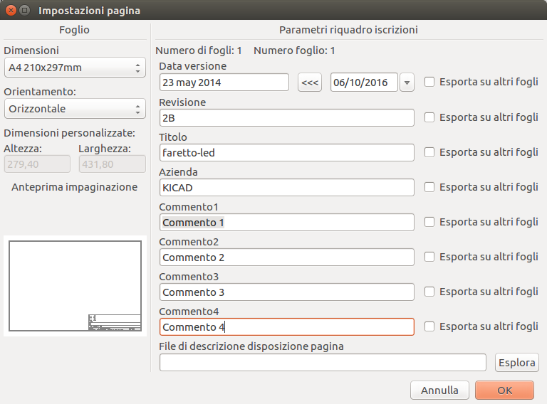
Each field in the title block can be edited, as well as the paper size and orientation. If the Export to other sheets option is checked for a field, that field will be updated in the title block of all sheets, rather than only the current sheet.
You can set the date to today’s or any other date by pressing the left arrow button next to Issue Date. Note that the date in the schematic will not be automatically updated.
A drawing sheet template file can also be selected.
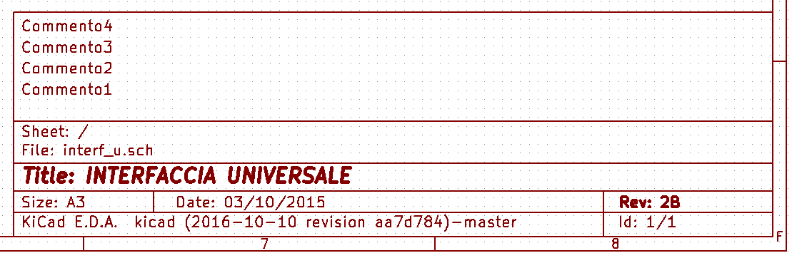
The sheet number (Sheet X/Y) is automatically updated, but sheet page numbers can also be manually set using Edit → Edit Sheet Page Number….
Impostazioni schema
La finestra Impostazioni schema viene utilizzata per impostare le opzioni dello schema che sono specifiche dello schema attualmente attivo. Ad esempio, la finestra contiene le opzioni di formattazione, la configurazione delle regole elettriche, l’impostazione della netclass e l’impostazione delle variabili di testo dello schema.
You can import schematic settings from an existing project using the Import Settings from Another Project… button. This allows you to choose a project to use as a template and select which settings to import (formatting preferences, field name templates, pin conflict map, violation severities, and net classes).
Schematic formatting
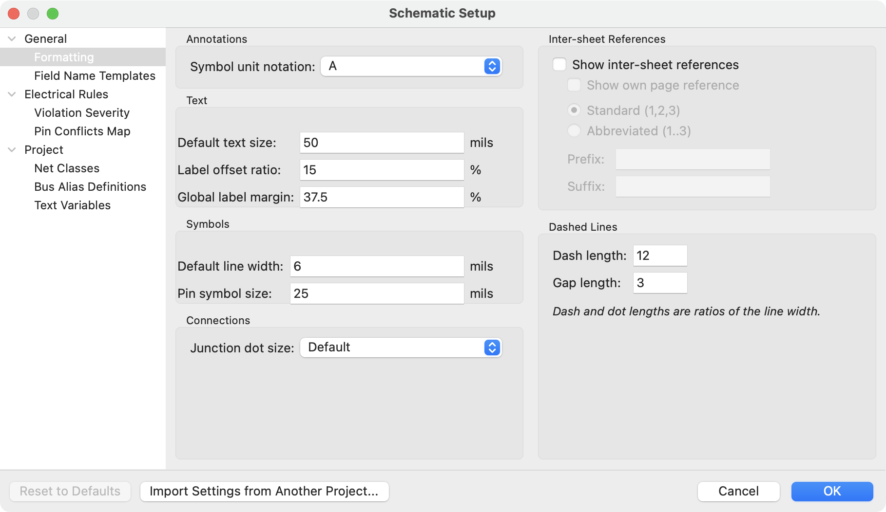
The formatting panel contains settings for the appearance of symbols, text, labels, graphics, and wires.
Symbol unit notation sets how each unit of a multi-unit symbol is referred to
in its reference designator. By default, a different letter for each unit is
appended to the reference designator with no separator, for example U1B for
the second unit of symbol U1, but this can be changed. Numbers can be used
instead of letters, and various separators can be used between the symbol
designator and the unit identifier (., -, _, or none).
Default text size sets the default text height used by the text, text box, and
label tools. Label offset ratio controls the vertical spacing between a local
label’s text and the attached wire, relative to the label’s text size. This also
affects the spacing between symbol pins and their pin number.
Global label margin defines the size of the box around a global label,
relative to the global label’s text size. Increasing the margin may be useful
to avoid overlapping text with overbars (~{}) or letters with descenders, but
this may cause closely packed global labels to overlap with each other.
Default line width sets the default line width for symbol graphics, if the symbol does not override the default line width. Pin symbol size scales symbol pin graphic style annotations, such as the bubble on an inverted pin.
Junction dot size sets the schematic’s default wire junction dot size. The default size can be overridden by editing an individual junction dot’s properties.
Show inter-sheet references enables or disables the display of
inter-sheet references, which are a list of page
numbers next to a global labels that link to other places in the schematic where
the same global label appears. Show own page reference controls whether the
current page is included in the list of page numbers. Standard and
abbreviated determine whether to display the complete list of page numbers or
only the first and last page numbers. The prefix and suffix fields add
optional characters before and after the list of page numbers. In the image
of an inter-sheet reference below, a prefix and suffix of [ and ],
respectively, have been added.
Dashed line appearance is controlled in the Formatting section. Dash length controls the length of dashes, while Gap length controls the spacing between dashes and dots. The dash and gap lengths are relative to the line width: a gap length of 2 means twice the width of the line.
Field name templates
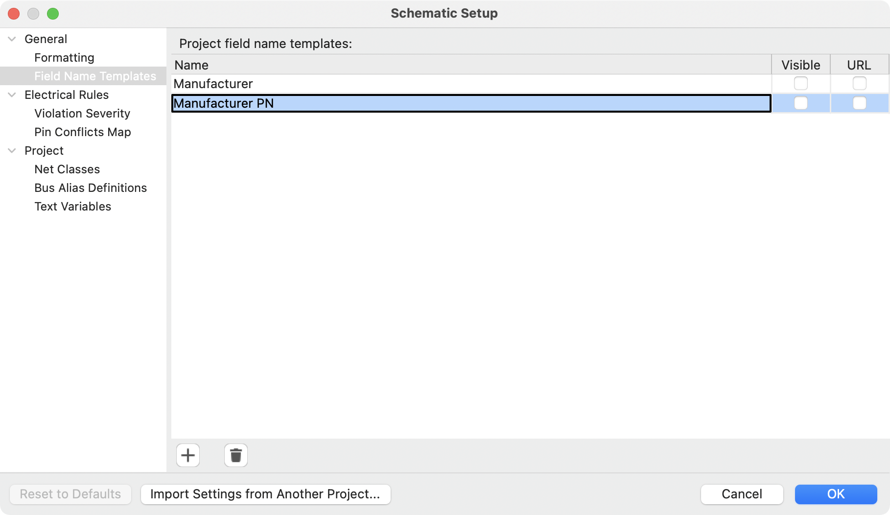
Field name templates are empty symbol fields that are automatically added to all symbols in the schematic. These can be useful when every symbol in the schematic needs additional fields beyond the fields that are defined in the library symbols, for example a field for the manufacturer’s part number.
Template fields can be set as visible or invisible, and can also be set as URL fields.
Field name templates that are defined in schematic setup apply only to the current project. Field name templates can also be defined in Preferences, which apply to all projects edited on your computer.
ERC violation severity and pin conflicts map
The Violation Severity panel lets you configure what types of ERC messages should be reported as Errors, Warnings, or ignored.
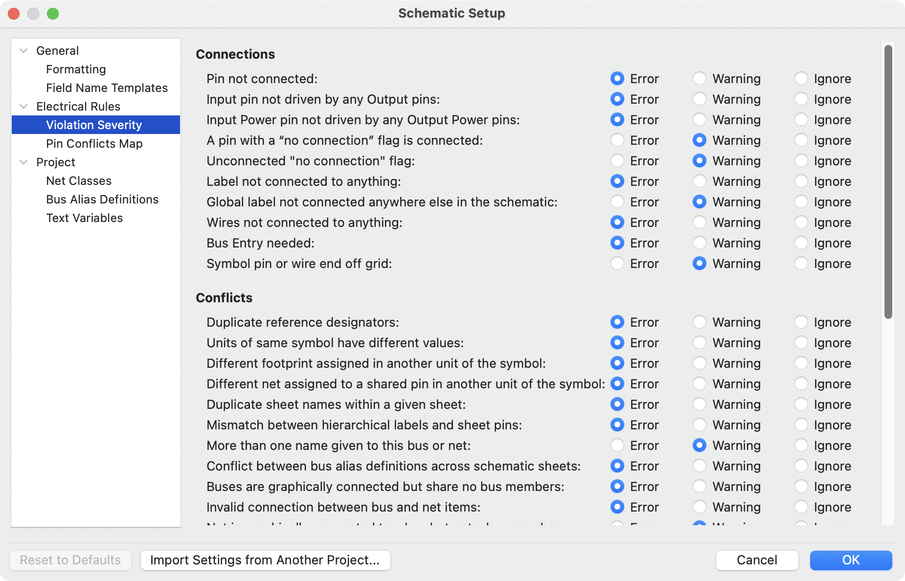
The Pin Conflicts Map allows you to configure connectivity rules to define electrical conditions for errors and warnings based on what types of pins are connected to each other. For example, by default an error is produced when an output pin is connected to another output pin.
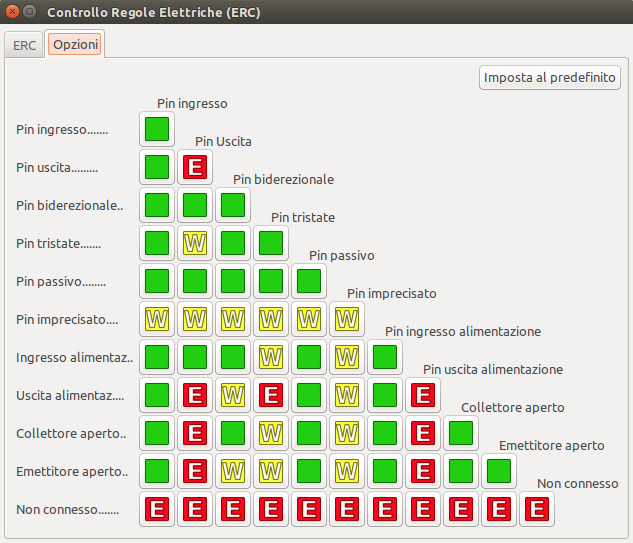
These panels are explained in more detail in the ERC section.
Net classes
The Net Classes panel allows you to manage netclasses for the project and assign nets to netclasses with patterns. Managing netclasses in this panel is equivalent to managing them in the Board Setup dialog. Nets can also be assigned to netclasses in the schematic using graphical assignments with net class directives or net labels.
Pattern-based netclass assigment is explained in more detail in the net classes section.
Bus alias definitions
The Bus Alias Definitions panel allows you to create bus aliases, which are names for groups of signals in a bus. For more information about bus aliases, see the bus alias documentation.
Variabili di testo
Text replacement variables can be created in the Text Variables section. These variables allow you to substitute the variable name for any text string. This substitution happens anywhere the variable name is used inside the variable replacement syntax of ${VARIABLENAME}.
For example, you could create a variable named VERSION and set the text substitution to 1.0. Now, in any text object on the PCB, you can enter ${VERSION} and KiCad will substitute 1.0. If you change the substitution to 2.0, every text object that includes ${VERSION} will be updated automatically. You can also mix regular text and variables. For example, you can create a text object with the text Version: ${VERSION} which will be substituted as Version: 1.0.
Text variables can also be created in Board Setup. Text variables are project-wide; variables created in the schematic editor are also available in the board editor, and vice versa.
There are also a number of built-in system text variables.
Opening legacy schematics
Modern versions of KiCad can always open projects created in older versions of KiCad. However, schematics created in some older versions of KiCad have special considerations that must be observed when opening them in order to prevent any data loss.
Opening KiCad 5.0 and 5.1 schematics
Modern versions of KiCad can open schematics created in versions prior to KiCad 6.0, but the cache library file (<projectname>-cache.lib) must be present to load the schematic correctly.
Since version 6.0, KiCad stores all symbols used in a project in the schematic. This means that you can open a schematic made in KiCad 6.0 or later on any computer, even if the libraries used in the project are not installed or have changed. Modern KiCad schematic files use the .kicad_sch extension.
Prior to version 6.0, KiCad did not store symbols in the schematic. Instead, KiCad stored references to the symbols and their libraries. It also stored a copy of every symbol used by the project in a separate cache library file (<projectname>-cache.lib). As long as the cache library was included with the project, the project could be distributed without the system library files, because KiCad could load any needed symbols from the cache library as a fallback if the libraries referenced in the schematic were missing. Legacy KiCad schematic files use the .sch extension.
When you open a legacy schematic, KiCad will look in the cache library to find all of the symbols used in the schematic in the cache library. When you save the legacy schematic, KiCad will save it as a new file in the modern schematic format (.kicad_sch), with the necessary symbols embedded in the schematic itself. The original legacy schematic and the cache library will remain, unmodified, but they are no longer necessary once the schematic has been saved in the modern format.
| Projects created in KiCad prior to version 6.0 must have a cache library. If the cache library is missing, the schematic will lose symbol information if the system symbol libraries are modified, reorganized, moved, or deleted. The libraries included with legacy versions of KiCad are substantially different than the modern KiCad libraries, so in practice KiCad will almost always fail to open legacy projects unless the cache library is present. |
When you open a legacy schematic, KiCad may display the Project Rescue Helper dialog. This means that one or more symbols in the cache library do not match the corresponding symbol in the external library. The dialog helps you "rescue" symbols from the cache library into your schematic, if desired. You can also open the rescue dialog at any time using Tools → Rescue Symbols…. The cache library file must be present in order to use the rescue tool.
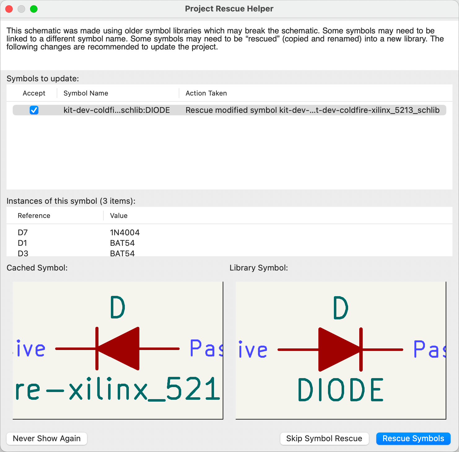
The rescue dialog lists all symbols that don’t match between the cache library and the external symbol library. The discrepancy can be because:
-
the cached symbol or the library symbol has been modified, so the two symbols no longer match, or
-
the cached symbol does not have a corresponding symbol in the symbol library, because the symbol or library was moved, renamed, deleted, or is not present on the current computer.
For each symbol in the list, selecting the symbol displays the reference designator and value for each instance of the symbol, and shows a visual preview of the symbol. If a corresponding symbol exists in the system symbol library, the dialog shows both copies of the symbol for comparison. If the symbol only exists in the cache library, the dialog only shows the cached symbol.
In this example, the project originally used a diode with the cathode facing left, but the library now contains one with the cathode facing right. This change would break the design, so it would be important to use the cached symbol as the original designer intended.
Pressing Rescue Symbols here will cause the selected symbols from the cache library to be saved into a special rescue library (<projectname>-rescue.kicad_sym). The corresponding symbols in the schematic will be updated to use the newly rescued symbols. Any unselected symbols will not be rescued, but their symbol linkage can be updated in the schematic later.
Alternatively, pressing Skip Symbol Rescue will exit the dialog without rescuing any symbols. KiCad will use the versions of the symbols found in the external libraries. You can run the rescue function again with Tools → Rescue Symbols…, or manually edit symbol linkage in the symbol’s properties.
If you would prefer not to see this dialog, you can press Never Show Again. This has the same effect as pressing Skip Symbol Rescue for the current schematic and all future schematics.
If a symbol in a legacy schematic cannot be found in either the cache library or the external library, KiCad cannot rescue that symbol. A placeholder symbol is inserted into the schematic in its place, as shown below.
You can attempt to remap these orphaned symbols using the Change Symbols or Edit Symbol Library Links dialogs, but either option may require manual corrections to the schematic. These tools are explained in more detail in the Updating and exchanging symbols section.
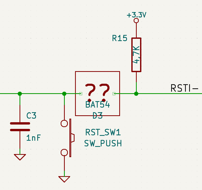
Opening pre-5.0 schematics
Modern versions of KiCad can open schematics created in versions prior to KiCad 5.0, but you will need to go through a symbol remapping process to open the schematic without losing symbol information.
Since version 5.0, KiCad schematics refer to specific symbols using both the symbol and library name. Even if multiple libraries each contain a symbol with the same name, the designer’s intended symbol is unambiguously specified.
Prior to version 5.0, KiCad schematics stored only the symbol name, not the library name. Symbols in the schematic were indirectly mapped back to the original library by searching through the project’s library list for a matching symbol. When you open a pre-5.0 schematic, KiCad will attempt to automatically "remap" the symbols so that each bare symbol name is replaced with a fully-specified symbol library and symbol name pair. The original schematics will be backed up in a rescue-backup folder.
You can skip the automatic remapping, but you will need to remap the symbols yourself using the Change Symbols dialog. You can also re-run the Remap Symbols tool using Tools → Remap Legacy Library Symbols….
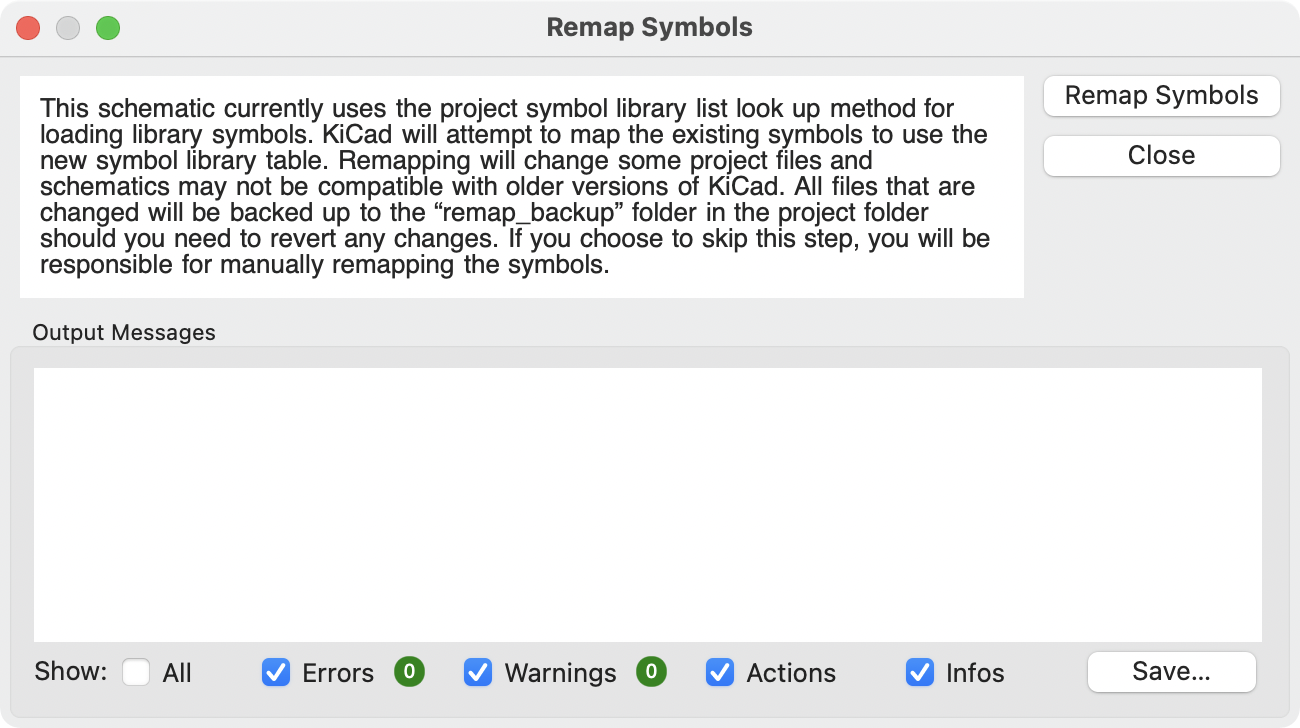
Schemi elettrici gerarchici
Introduzione
In KiCad, multi-sheet schematics are hierarchical: there is a single root sheet, and additional sheets are created as subsheets of either the root sheet or another subsheet. Sheets can be included in a hierarchy multiple times, if desired.
Carefully drawing a schematic as a hierarchical design improves schematic legibility and reduces repetitive drawing.
Creating a hierarchical schematic starts from the root sheet. The process is to create a subsheet, then draw the circuit in the subsheet and make the necessary electrical connections between sheets. Connections can be made between nets in a subsheet and nets in the parent sheet using hierarchical pins and labels, or between any two nets in the hierarchy using global labels.
Adding sheets to a design
You can add a subsheet to a design with the Add Hierarchical Sheet tool (S hotkey, or the ![]() button in the right toolbar). Launch the tool, then click twice in the canvas to draw the upper left and lower right corners of the subsheet symbol. Make the sheet outline large enough to fit the hierarchical pins you will add later.
button in the right toolbar). Launch the tool, then click twice in the canvas to draw the upper left and lower right corners of the subsheet symbol. Make the sheet outline large enough to fit the hierarchical pins you will add later.
The Sheet Properties dialog will appear and prompt you for a sheet name and filename.
The sheet name must be unique, as it is used in the full net name for any nets in the subsheet. For example, a net with the local label net1 in the sheet sheet1 would have a full net name of /sheet1/net1. The sheet name is also used to refer to the sheet in various places in the GUI, including the title block and the hierarchy navigator.
The sheet file specifies the file that the new sheet will be saved to or loaded from. The path to the sheet file can be relative or absolute. It is usually preferable to save subsheet files in the project directory and use a relative path so that the project is portable.
A single sheet file can be used more than once in a project by specifying the same filename for each repeated sheet; the circuit drawn in the sheet will be instantiated once per usage, and any edits in once instance will be reflected in the other instances.
| Sheet files can be shared between multiple projects to allow design reuse between projects. However, this is not recommended due to path portability concerns and the risk of unintentionally changing other projects while editing a shared sheet. |
The sheet’s page number is configurable here. The page number is displayed in the sheet title block and the hierarchy navigator, and sheets are sorted by page number in the hierarchy navigator and when printing or plotting.
Several graphical options are also available. Border width sets the width of the border around the sheet shape. Border color and Background fill set the color for the border and fill of the sheet shape, respectively. If no color is set, a checkerboard swatch is shown and the default values from the color theme are used.
Sheets support arbitrary custom fields, which can be added and removed with the ![]() and
and ![]() buttons, respectively. Sheet fields can be optionally displayed on the schematic by checking their Show box, and they can be accessed from inside the sheet or in other sheet fields using text variables.
buttons, respectively. Sheet fields can be optionally displayed on the schematic by checking their Show box, and they can be accessed from inside the sheet or in other sheet fields using text variables.
The Sheet Properties dialog can be accessed at any time by selecting a sheet symbol and using the E hotkey, or by right-clicking on a sheet symbol and selecting Properties….
Navigating between sheets
You can enter a hierarchical sheet from the parent sheet by double-clicking the child sheet’s shape, or right-clicking the child sheet and selecting Enter Sheet.
Return to the parent sheet by using the ![]() button in the top toolbar, or by right-clicking in an empty part of the schematic and clicking Leave Sheet.
button in the top toolbar, or by right-clicking in an empty part of the schematic and clicking Leave Sheet.
You can jump to the next sheet with the ![]() button, or to the previous sheet with the
button, or to the previous sheet with the ![]() button.
button.
Alternatively, you can jump to any sheet with the hierarchy navigator. To open the hierarchy navigator, click the ![]() button in the left toolbar. The hierarchy navigator docks at the left of the screen. Each sheet in the design is displayed as an item in the tree. Clicking a sheet name opens that sheet in the editing canvas.
button in the left toolbar. The hierarchy navigator docks at the left of the screen. Each sheet in the design is displayed as an item in the tree. Clicking a sheet name opens that sheet in the editing canvas.
Connessioni elettriche tra fogli
Panoramica etichette
Electrical connections between sheets are made with labels. There are several kinds of labels in KiCad, each with a different connection scope.
-
Local labels only make connections within a sheet. Therefore local labels cannot be used to connect between sheets. Local labels are added with the
button. -
Global labels make connections anywhere in a schematic, regardless of sheet. Global labels are added with the
button. -
Le etichette gerarchiche si connettono ai pin del foglio gerarchico accessibili nel foglio principale. I progetti gerarchici si basano su etichette e pin gerarchici per creare connessioni tra fogli padre e fogli figli; si può pensare ai pin gerarchici come mezzi per definire l’interfaccia per un foglio. Le etichette gerarchiche vengono aggiunte con il pulsante
.
| Labels that have the same name will connect, regardless of the label type, if they are in the same sheet. |
| Hidden power pins can also be considered global labels, because they connect anywhere in the schematic hierarchy. |
Pin fogli gerarchici
After placing hierarchical labels within the subsheet, matching hierarchical pins can be added to the subsheet symbol in the parent sheet. You can then make connections to the hierarchical pins with wires, labels, and buses. Hierarchical pins in a subsheet symbol are connected to the matching hierarchical labels in the subsheet itself.
| Hierarchical labels must be defined in the subsheet before the corresponding hierarchical sheet pin can be imported in the sheet symbol. |
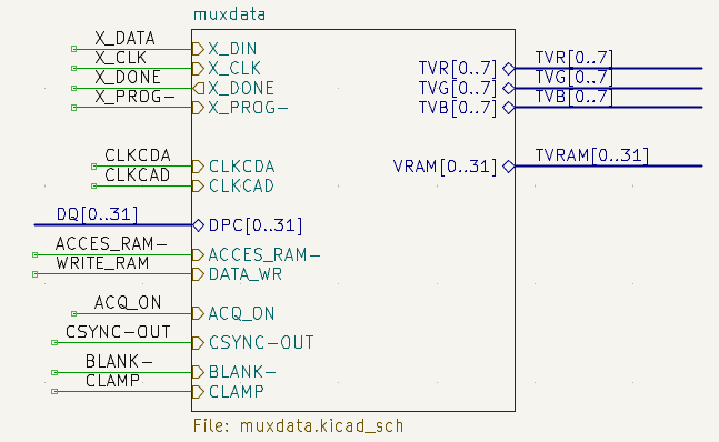
Per ogni etichetta gerarchica nel sottofoglio, importare il pin gerarchico corrispondente nel simbolo del foglio facendo clic sul pulsante ![]() nella barra degli strumenti a destra, quindi facendo clic sul simbolo del foglio. Un segnaposto per la prima etichetta gerarchica senza corrispondenza verrà attaccato al puntatore, dove può essere posizionato ovunque lungo il bordo del simbolo del foglio. Facendo nuovamente clic con lo strumento si continuerà ad importare ulteriori pin del foglio fino a quando non ci saranno più pin gerarchici da importare dal sottofoglio. I pin foglio possono essere importati anche selezionando Importa pin fogli nel menu contestuale del simbolo del foglio.
nella barra degli strumenti a destra, quindi facendo clic sul simbolo del foglio. Un segnaposto per la prima etichetta gerarchica senza corrispondenza verrà attaccato al puntatore, dove può essere posizionato ovunque lungo il bordo del simbolo del foglio. Facendo nuovamente clic con lo strumento si continuerà ad importare ulteriori pin del foglio fino a quando non ci saranno più pin gerarchici da importare dal sottofoglio. I pin foglio possono essere importati anche selezionando Importa pin fogli nel menu contestuale del simbolo del foglio.
You can edit the properties of a sheet pin in the Sheet Pin Properties dialog. Open this dialog by double-clicking a sheet pin, selecting a sheet pin and using the E hotkey, or right-clicking a sheet pin and selecting Properties….
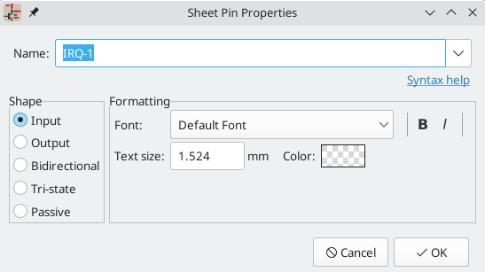
The sheet pin’s name can be edited in the textbox or by selecting from the dropdown list of hierarchical labels in the subsheet. A sheet pin’s name has to match the corresponding hierarchical label in the subsheet, so if a pin name is changed the label must change as well.
Shape changes the shape of the sheet pin, and has no electrical effect. It can be set to Input, Output, Bidirectional, Tri-state, or Passive. The pin’s font, text size, color, and emphasis (bold or italic) can also be changed.
Esempi di progettazioni gerarchiche
I disegni gerarchici possono essere classificati in diverse categorie:
-
Semplice: ogni foglio viene usato solo una volta.
-
Complessa: alcuni fogli sono istanziati più volte.
-
Piatta: sottocaso di gerarchia Semplice, senza connessioni tra i sottofogli e il loro genitore. Le gerarchie piatte possono essere usate per rappresentare una progettazione non gerarchica.
Ogni modello gerarchico può essere utile; quello più appropriato dipende dal progetto.
Gerarchia semplice
An example of a simple hierarchy is the video demo project included with KiCad. The root sheet contains seven unique subsheets, each with hierarchical labels and sheet pins linking the sheets to each other in the root sheet. Two of the subsheet symbols are shown below.
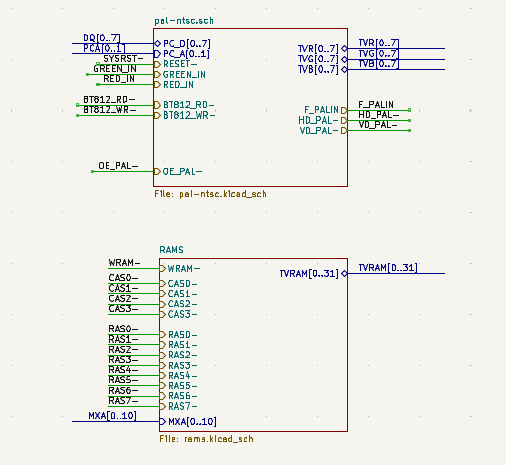
Gerarchia complessa
The complex_hierarchy demo project is an example of a complex hierarchy. The root sheet contains two subsheet symbols, which both refer to the same sheet file (ampli_ht.kicad_sch). This allows the design to include two copies of the same amplifier circuit. Although the two sheet symbols refer to the same filename, the sheet names are unique (ampli_ht_vertical and ampli_ht_horizontal). Inside each subsheet the circuits are identical except for the reference designators, which as always are unique.
This project contains no sheet pin connections. The only connections between the root sheet and the subsheets are global power connections made with power symbols. However, sheets in a complex hierarchy could include sheet pin connections if appropriate for the design.
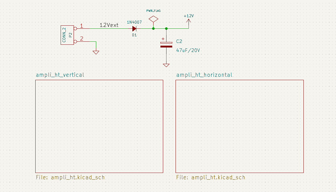
Gerarchia piatta
The flat_hierarchy demo project is an example of a flat hierarchy. The root sheet contains two unique subsheet symbols with no hierarchical sheet pins. The root sheet in this project does nothing except hold the subsheets, and the subsheets are used only as additional pages in the schematic.
| This is the simplest way to create multi-page schematics in KiCad. |
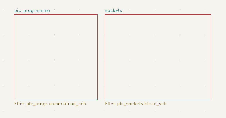
Ispezione di uno schema
Strumento trova
The Find tool searches for text in the schematic, including reference designators, pin names, symbol fields, and graphic text. When the tool finds a match, the canvas is zoomed and centered on the match and the text is highlighted. Launch the tool using the ![]() button in the top toolbar.
button in the top toolbar.
Lo strumento trova ha diverse opzioni:
Match case: Selects whether the search is case-sensitive.
Words: When selected, the search will only match the search term with complete words in the schematic. When unselected, the search will match if the search term is part of a larger word in the schematic.
Wildcards: When selected, wildcards can be used in the search terms. ?
matches any single character, and * matches any number of characters. Note
that when this option is selected, partial matches are not returned: searching
for abc* will match the string abcd, but searching for abc will not.
Search pin names and numbers: Selects whether the search should apply to pin names and numbers.
Search hidden fields: Selects whether the search should apply only to visible fields or if it should include hidden symbol fields.
Search the current sheet only: Selects whether the search should be limited to the current schematic sheet or to the entire schematic.
There is also a Find and Replace tool which is activated with the ![]() button in the top toolbar. This tool behaves the same as the Find tool, but additionally can replace some or all matches with different text.
button in the top toolbar. This tool behaves the same as the Find tool, but additionally can replace some or all matches with different text.
If the Replace matches in reference designators option is checked, reference designators will be modified if they contain matching text. Otherwise reference designators will not be affected.
Evidenziazione net
An electrical net can be highlighted in the schematic editor to visualize all of the places it appears in the schematic. Net highlighting can be activated in the Schematic Editor or by highlighting the corresponding net in the PCB editor when cross-probe highlighting is enabled (see below). When net highlighting is active, the highlighted net will be shown in a different color. By default this color is pink, but it is configurable in the Color section of the Preferences dialog.
Nets can be highlighted by clicking on a wire or pin using the Highlight Net tool in the right toolbar (![]() ). Alternatively, the Highlight Net hotkey (`) highlights the net under the cursor.
). Alternatively, the Highlight Net hotkey (`) highlights the net under the cursor.
Net highlighting can be cleared by using the Clear Net Highlight action (hotkey ~) or by using the Highlight net tool on an empty region in the schematic. By default, Esc also clears net highlighting, but this can be disabled if desired in Preferences → Schematic Editor → Editing Options.
Cross-probing from the PCB
KiCad allows bi-directional cross-probing between the schematic and the PCB. There are several different types of cross-probing.
Selection cross-probing allows you to select a symbol or pin in the schematic to select the corresponding footprint or pad in the PCB (if one exists) and vice-versa. By default, cross-probing will result in the display centering on the cross-probed item and zooming to fit. This behavior can be disabled in the Display Options section of the Preferences dialog.
Highlight cross-probing allows you to highlight a net in the schematic and PCB at the same time. If the option "Highlight cross-probed nets" is enabled in the Display Options section of the Preferences dialog, highlighting a net or bus in the schematic editor will cause the corresponding net or nets to be highlighted in the PCB editor, and vice versa.
Controllo Regole Elettriche (ERC)
Lo strumento per il controllo regole elettriche (ERC) controllo la presenza di certi errori presenti nello schema, come piedini sconnessi, simboli gerarchici sconnessi, uscite in corto-circuito, o altri tipi di connessioni non consentite, ecc. Le violazioni vengono segnalate come errori o avvisi a seconda della gravità del problema rilevato.
ERC è imperfetto e non è in grado di rilevare tutti gli errori, ma può rilevare molti problemi e sviste comuni. Tutti i problemi rilevati devono essere controllati e risolti prima di procedere. La qualità dell’ERC è direttamente correlata alla cura posta nel dichiarare le proprietà elettriche del pin durante la creazione del simbolo. Se i simboli sono progettati in modo errato, ERC non riporterà informazioni accurate.
l’ERC può essere avviato facendo clic sul pulsante ![]() nella barra strumenti in cima e facendo clic sul pulsante Esegui ERC.
nella barra strumenti in cima e facendo clic sul pulsante Esegui ERC.
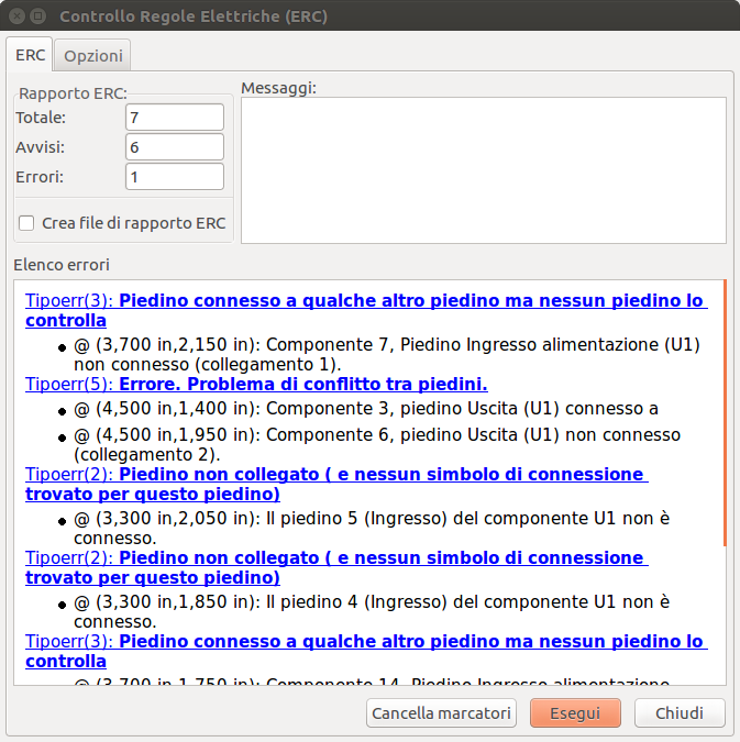
Any warnings or errors are reported in the Violations tab, and markers for each violation are placed in the schematic so that they point to the relevant part of the schematic. Warnings are indicated by yellow arrows, and errors have red arrows. Excluded violations are shown as green arrows.
| Selezionando una violazione nella finestra ERC si passa al marcatore di violazione selezionato nello schema. |
The numbers at the bottom of the window show the number of errors, warnings, and exclusions. Each type of violation can be filtered from the list using the respective checkboxes. Clicking Delete Markers will clear all violations until ERC is run again.
Violations can be right-clicked in the dialog to ignore them or change their severity:
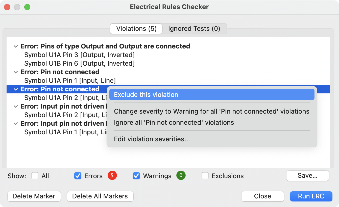
-
Exclude this violation: ignores this particular violation, but does not affect any other violations.
-
Change severity: changes a type of violation from warning to error, or error to warning. This affects all violations of a given type.
-
Ignore all: ignores all violations of a given type. This test will now appear in the Ignored Tests tab rather than the Violations tab.
You can also exclude the selected marker with Inspect → Exclude Marker, and show or hide each category of marker (errors, warnings, and exclusions) with the View menu.
Excluded and ignored violations are remembered between runs of the design rule checker.
Esempio di ERC
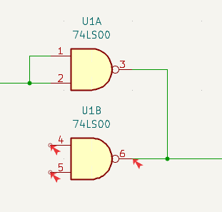
There are three errors in the screenshot above.
-
Due uscite sono state collegate assieme (freccia rossa sulla destra).
-
Two inputs have been left unconnected (red arrows at left). This is actually two errors per pin: each pin is unconnected, and each pin is an input pin that is not driven by an output pin.
Selecting an ERC marker displays a description of the violation in the message pane at the bottom of the window.
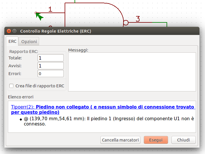
Piedini e segnalazioni di potenza
It is common to have an "Input Power pin not driven by any Output Power pins" error on power pins, as shown in the example below, even though the power pins seem to be properly connected to a power rail. This happens in designs where the power is provided through connectors or other components that are not marked as power outputs. In these cases ERC won’t detect any Output Power pins connected to the net and will determine the Input Power pin is not driven by a power source.
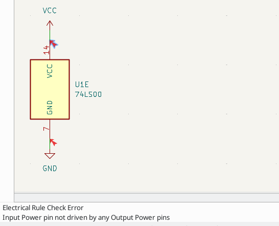
To avoid this warning, connect the net to PWR_FLAG symbol on such a power net as shown in the following example. The PWR_FLAG symbol is found in the power symbol library. Alternatively, connect any power output pin to the net; PWR_FLAG is simply a symbol with a single power output pin.
Le reti di massa spesso necessitano anche di un PWR_FLAG, poiché i regolatori di tensione hanno uscite dichiarate come uscite di potenza, ma i loro pin di massa sono tipicamente contrassegnati come ingressi di alimentazione. Pertanto le masse possono apparire non collegate a una fonte a meno che non venga utilizzato un simbolo PWR_FLAG.
For more information about power pins and power flags, see the PWR_FLAG documentation.
Configurazione ERC
Il pannello Importanza violazione nella Impostazione dello schema permette di configurare che tipo di messaggi ERC devono essere riportati come errori, come semplici avvertimenti o ignorati.
Il pannello Mappa conflitti pin nelle Impostazioni dello schema, permette di configurare le regole di connessione per definire le condizioni elettriche per il controllo di errori e avvertimenti in base al tipo di pin connesso uno con l’altro. Ad esempio, per impostazione predefinita viene prodotto un errore quando un pin di uscita è collegato a un altro pin di uscita.
Le regole si possono cambiare facendo clic sul riquadro desiderato della matrice, in modo ciclare la scelta desiderata: normale, avvertimento, errore.
Elenco controlli ERC
The table below lists the electrical rules that KiCad checks and the default violation severity for each check. All severities are configurable.
| Violation | Description | Default Severity |
|---|---|---|
Pin not connected |
All symbol pins must be connected to a net, unless the pin has a no-connect flag or has electrical type Unconnected. |
Error |
Input pin not driven by any Output pins |
All Input pins must be connected to an Output pin. |
Error |
Input Power pin not driven by any Output Power pins |
All Input Power pins must be connected to an Output Power pin. A common cause of this violation is described above. |
Error |
A pin with a "no connection" flag is connected |
Pins with no connection flags cannot be connected to anything else. |
Warning |
Unconnected "no connection" flag |
No connection flags cannot be left unconnected. They must be connected to a pin or label. |
Warning |
Label not connected to anything |
Global, hierarchical, and local labels must be connected to a pin or another label. |
Error |
Global label not connected anywhere else in the schematic |
Global labels need at least two other pins on the same net; otherwise they are not connecting anything. |
Warning |
Wires not connected to anything |
Wires must be connected to a pin or label. |
Error |
Bus Entry needed |
This violation only applies to projects imported from EAGLE projects. It indicates places where the importer was unable to automatically add bus entries to the imported schematic, so you must add them by hand. |
Error |
Symbol pin or wire end off grid |
Symbol pins and wire ends need to be aligned to the grid in order to connect to each other. |
Warning |
Duplicate reference designators |
Two symbols cannot have the same reference designator. |
Error |
Units of same symbol have different values |
All units of a single symbol must have the same value. |
Error |
Different footprint assigned in another unit of the symbol |
All units of a single symbol must have the same footprint assigned. |
Error |
Different net assigned to a shared pin in another unit of the symbol |
Any pins that are shared between multiple units of a symbol must have the same net connected across all units. |
Error |
Duplicate sheet names within a given sheet |
All hierarchical sheets within a given sheet must have unique names. |
Error |
Mismatch between hierarchical labels and sheet pins |
All hierarchical labels must have a corresponding hierarchical sheet pin in the parent sheet, and all hierarchical sheet pins must have a matching hierarchical label in the child sheet. |
Error |
More than one name given given to this bus or net |
Nets can only have a single name, so if multiple labels are attached to a net, one name will be selected and used as the canonical name. |
Warning |
Conflict between bus alias definitions across schematic sheets |
If the same bus alias name is used in multiple sheets, the members of the alias must be the same for each sheet. |
Error |
Buses are graphically connected but share no bus members |
Buses that are graphically connected must have bus members in common. |
Error |
Invalid connection between bus and net items |
Buses cannot be connected to net items such as wires, labels referring to single nets, or sheet pins referring to single nets. Labels and sheet pins can only be connected to buses if they refer to buses rather than individual signals. |
Error |
Net is graphically connected to a bus but not a bus member |
Nets can only be connected to a bus with a bus entry if they are a member of the bus. |
Warning |
Conflicting netclass assignments |
Only one netclass can be assigned to a net. |
Error |
Symbol is not annotated |
Symbols must be annotated with a unique reference designator. |
Error |
Unresolved text variable |
Text variables ( |
Error |
SPICE model issue |
SPICE models must not have syntax errors or other problems. |
Error |
Labels are similar (lower/upper case difference only) |
If two labels are similar and differ only by the case of some letters, this may be a typo causing two labels to be disconnected when they are intended to be connected. |
Warning |
Library symbol issue |
Several symbol library issues are checked:
|
Warning |
Symbol has more units than are defined |
Symbols cannot have more units placed in the schematic than are defined in the symbol. Units in the schematic must correspond exactly to the symbol definition. |
Error |
Symbol has units that are not placed |
All of the units in a multi-unit symbol should be placed in the schematic. |
Warning |
Symbol has input pins that are not placed |
A multi-unit symbol has units with input pins that are not placed, so those input pins will not be connected to anything. All units with input pins should be placed in the schematic. |
Warning |
Symbol has bidirectional pins that are not placed |
A multi-unit symbol has units with bidirectional pins that are not placed, so those bidirectional pins will not be connected to anything. All units with bidirectional pins should be placed in the schematic. |
Warning |
Symbol has power input pins that are not placed |
A multi-unit symbol has units with power input pins that are not placed, so those power input pins will not be connected to anything. All units with power input pins should be placed in the schematic. |
Error |
Conflict problem between pins |
Connections between pins must match the allowed connections in the Pin Conflicts Map. |
From Pin Conflicts Map |
File rapporto ERC
Un file di rapporto ERC può essere generato e salvato facendo clic sul pulsante Salva… nella finestra di dialogo ERC. L’estensione file per i file rapporto ERC è .rpt. Ecco un file rapporto ERC di esempio.
Rapporto ERC (ven 21 ott 2022 02:07:05 PM EDT, codifica UTF8)

***** Foglio /
[pin_not_driven]: pin d'ingresso non pilotato da nessun pin d'uscita
    ; Severity: error
    @(149.86 mm, 60.96 mm): Symbol U1B [74LS00] Pin 4 [, Input, Line]
[pin_not_connected]: pin non connesso
    ; Severity: error
    @(149.86 mm, 60.96 mm): Symbol U1B [74LS00] Pin 4 [, Input, Line]
[pin_not_connected]: pin non connesso
    ; Severity: error
    @(149.86 mm, 66.04 mm): Symbol U1B [74LS00] Pin 5 [, Input, Line]
[pin_to_pin]: pin di tipo uscita e uscita sono connessi
    ; Severity: error
    @(165.10 mm, 63.50 mm): Symbol U1B [74LS00] Pin 6 [, Output, Inverted]
    @(165.10 mm, 46.99 mm): Symbol U1A [74LS00] Pin 3 [, Output, Inverted]
[pin_not_driven]: pin d'ingressno non pilotato da nessun pin d'uscita
    ; Severity: error
    @(149.86 mm, 66.04 mm): Symbol U1B [74LS00] Pin 5 [, Input, Line]

 ** Messaggi ERC 5,  Errori 5,  Avvertimenti 0
Assegnazione impronte
Prima di sbrogliare un C.S., è necessario selezionare le impronte per ogni componente che verrà assemblato sulla scheda. Le impronte definiscono le connessioni in rame tra i componenti fisici e le tracce sbrogliate su un circuito stampato.
Alcuni simboli vengono forniti con impronte preassegnate, ma per molti simboli ci sono più impronte possibili, quindi l’utente deve selezionare quella appropriata.
KiCad offre diversi metodi per assegnare impronte:
-
Proprietà del simbolo
-
Finestra proprietà del simbolo
-
Tabella campi del simbolo
-
-
Mentre si piazzano i simboli
-
Strumento di assegnamento impronte
Ogni metodo verrà spiegato di seguito. Quale usare è una questione di preferenze; un metodo può essere più conveniente a seconda della situazione. Tutti questi metodi sono equivalenti in quanto memorizzano il nome dell’impronta selezionata nel campo Impronta del simbolo.
| La tabella librerie impronte deve essere configurata prima che le impronte possano essere assegnate. Per informazioni sulla configurazione della tabella libreria impronte, consultare il manuale dell’editor di circuiti stampati. |
Assegnare impronte nelle proprietà del simbolo
Il campo Impronta di un simbolo può essere modificato direttamente nella finestra Proprietà del simbolo.
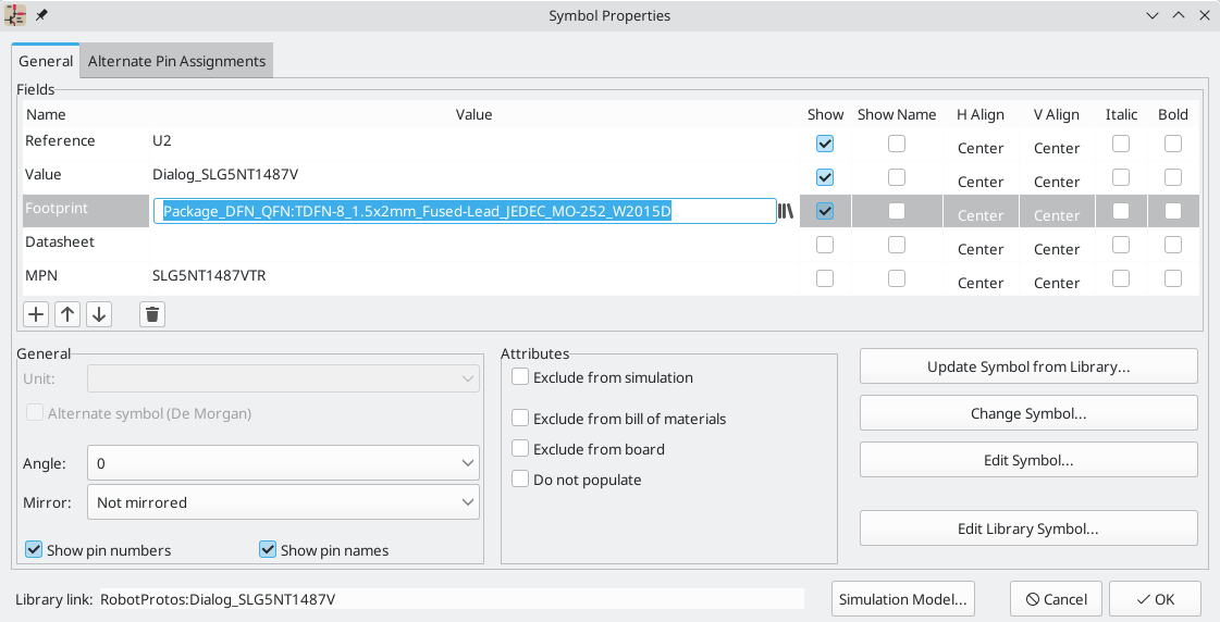
Facendo clic sul pulsante ![]() nel campo
nel campo Impronta si apre l’Esploratore librerie di impronte, che mostra le impronte disponibili e le librerie di impronte. Un singolo clic sul nome di un’impronta seleziona l’impronta e la visualizza nel riquadro di anteprima a destra, mentre il doppio clic su un’impronta chiude l’esploratore e imposta il campo Impronta del simbolo all’impronta selezionata.
Assegnamento impronte con la tabella campi del simbolo
Anziché modificare singolarmente le proprietà di ciascun simbolo, è possibile utilizzare la Tabella campi simbolo per visualizzare e modificare le proprietà di tutti i simboli nel disegno da un unico posto. Ciò include l’assegnazione di impronte modificando il campo Impronta di ciascun simbolo.
La tabella campi simbolo è accessibile tramite Strumenti → Modifica i campi del simbolo…, o con il pulsante ![]() nella barra in alto.
nella barra in alto.
Il campo Impronta qui si comporta come nella finestra delle proprietà del simbolo: può essere modificato direttamente o le impronte possono essere selezionate visivamente con l’Esploratore librerie di impronte.
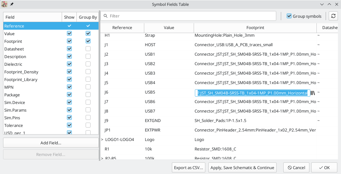
Per ulteriori informazioni sulla tabella dei campi dei simboli, vedere la sezione modifica proprietà simboli.
Assegnazione impronte piazzando simboli
Le impronte possono essere assegnate ai simboli quando il simbolo viene aggiunto per la prima volta allo schema.
Alcuni simboli sono definiti con una impronta predefinita. Questi simboli avranno questa impronta preassegnata quando verranno aggiunti allo schema. L’impronta predefinita è visibile nella finestra di dialogo Aggiungi simbolo. Per i simboli senza una impronta predefinita definita, il menu a discesa dell’impronta indicherà "Nessuna impronta predefinita" e l’area di anteprima dell’impronta indicherà "Nessuna impronta specificata".
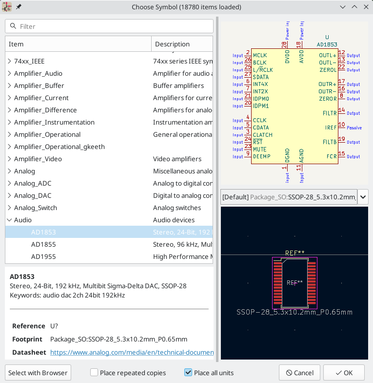
I simboli possono avere filtri impronte che specificano quali impronte sono appropriate per un dato simbolo. Se il filtro impronte è definito per il simbolo selezionato, tutte le impronte che avranno un riscontro con il filtro appariranno come opzioni nell’elenco a discesa impronte. L’impronta selezionata verrà visualizzata nell’area di anteprima e verrà assegnata al simbolo quando il simbolo verrà aggiunto allo schema.
| Le opzioni impronte non appariranno nell’elenco a discesa delle impronte se non vengono caricate le librerie di impronte. Le librerie di impronte vengono caricate la prima volta che l’Editor impronte o l’Esploratore librerie di impronte vengono aperti in una sessione. |
Per ulteriori informazioni sui filtri impronte, vedere Documentazione dell’editor dei simboli.
Assegnamento impronte tramite lo strumento di assegnamento impronte
Lo strumento di assegnazione impronte consente di associare i simboli nello schema alle impronte usate durante la disposizione del circuito stampato. Fornisce un elenco filtrabile di impronte, la visualizzazione delle impronte e la visualizzazione 3D del modello del componente, per aiutare nella verifica della corretta associazione dell’impronta al componente.
I componenti possono essere assegnati alle loro impronte corrispondenti manualmente o automaticamente creando i file di equivalenze (file .equ). I file delle equivalenze sono tabelle di corrispondenza che associano ogni componente alla sua impronta.
Eseguire lo strumento con Strumenti → Assegna impronte… o facendo clic sull’icona ![]() nella barra degli strumenti in alto.
nella barra degli strumenti in alto.
Panoramica dello strumento di assegnamento impronte
L’immagine sottostante mostra la finestra principale dello strumento assegnamento impronte.
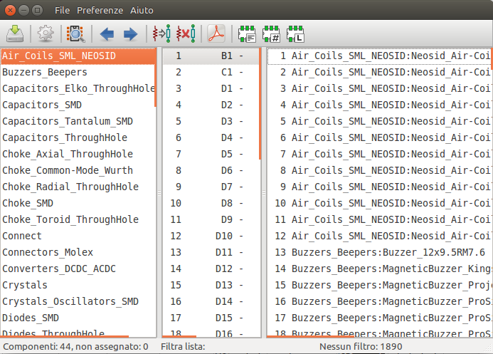
-
Il riquadro a sinistra contiene l’elenco delle librerie di impronte disponibili associate al progetto.
-
Il pannello centrale contiene l’elenco dei simboli nello schema.
-
Il pannello di destra contiene l’elenco delle impronte disponibili caricate dalle librerie di impronte del progetto.
-
Il pannello in basso descrive i filtri che sono stati applicati all’elenco impronte e visualizza le informazioni sull’impronta selezionata nel pannello più a destra.
La barra superiore contiene i seguenti comandi:
|
Transferisci le associazioni impronte correnti allo schema elettrico. |
|
Modifica le tabelle librerie impronte globali e del progetto. |
|
Visualizza l’impronta selezionata nel visualizzatore impronte. |
|
Seleziona il simbolo precedente senza associazione impronta. |
|
Seleziona il simbolo successivo senza associazione impronta. |
|
Annulla l’ultima modifica. |
|
Ripete l’ultima modifica. |
|
Esegue l’associazione automatica impronte usando un file di equivalenze. |
|
Elimina tutte le assegnazioni impronte. |
|
Filtra l’elenco impronte usando i filtri impronte definiti nel simbolo selezionato. |
|
Filtra l’elenco impronte usando il numero di pin del simbolo selezionato. |
|
Filtra l’elenco impronte usando la libreria selezionata. |
La seguente tabella elenca i comandi da tastiera per l’assegnamento impronte.
Freccia destra / Tab |
Attiva il pannello adiacente a destra del pannello attualmente attivo. A capo al primo pannello se è attivo l’ultimo pannello. |
Freccia sinistra |
Attiva l’adiacente pannello a sinistra del pannello attualmente attivo. A capo all’ultimo pannello se è attivo il primo pannello. |
Freccia su |
Seleziona l’elemento precedente all’elemento attualmente selezionato. |
Freccia giù |
Seleziona l’elemento successivo all’elemento attualmente selezionato. |
Pagina su |
Seleziona l’elemento di una pagina precedente all’elemento attualmente selezionato. |
Pagina giù |
Seleziona l’elemento di una pagina successiva all’elemento attualmente selezionato. |
Home |
Seleziona il primo elemento dell’elenco attualmente selezionato. |
Fine |
Seleziona l’ultimo elemento dell’elenco attualmente selezionato. |
Associazione manuale delle impronte con lo strumento assegnamento impronte
Per associare manualmente una impronta ad un componente, bisogna prima selezionare un componente nel pannello componenti (centro). Poi selezionare un’impronta nel pannello delle impronte (destra) facendo doppio clic con il pulsante sinistro del mouse sul nome dell’impronta desiderata. L’impronta verrà assegnata al componente selezionato, ed il prossimo componente senza un’impronta assegnata verrà automaticamente selezionato.
| Se non vengono visualizzate impronte nel pannello impronte, verificare che le opzioni filtro impronte siano state applicate correttamente. |
Quando a tutti i componenti sono state assegnate impronte, fare clic sul pulsante OK per salvare le assegnazioni e uscire dallo strumento. In alternativa, fare clic su Annulla per eliminare le assegnazioni aggiornate o su Applica, salva schema e continua per salvare le nuove assegnazioni senza uscire dallo strumento.
Filtro dell’elenco impronte
Sono disponibili quattro opzioni di filtro che limitano le impronte visualizzate nel pannello impronte. Le opzioni di filtro sono abilitate e disabilitate con tre pulsanti e una casella di testo nella barra degli strumenti in alto.
-
 : Attiva filtri che possono essere definiti in ogni simbolo. Ad esempio, un simbolo opamp potrebbe definire filtri che mostrano solo impronte SOIC e DIP.
 -
 : mostra solo impronte che corrispondono al numero di pin del simbolo selezionato.
 -
 : mostra solo le impronte della libreria selezionata nel riquadro di sinistra.
 -
L’inserimento di testo nella casella nasconde le impronte che non corrispondono al testo. Questo filtro è disabilitato quando la casella è vuota.
Quando tutti i filtri sono disattivati, viene visualizzato l’elenco completo delle impronte.
I filtri applicati sono descritti nel riquadro inferiore della finestra, insieme al numero di impronte che soddisfano i filtri selezionati. Ad esempio, quando i filtri impronte e i filtri conteggio pin simbolo sono abilitati, il riquadro inferiore stampa i filtri impronta e conteggio pin:
È possibile utilizzare più filtri contemporaneamente per restringere l’elenco impronte eventualmente appropriate nel riquadro delle impronte. I simboli nella libreria standard di KiCad definiscono i filtri impronte progettati per essere utilizzati in combinazione con i filtri conteggio pin.
Associazione automatica di impronte con lo strumento di assegnamento impronte
Lo strumento di assegnazione impronte consente di memorizzare le assegnazioni delle impronte in un file esterno e di caricare le assegnazioni in un secondo momento, anche in un progetto diverso. Ciò consente di associare automaticamente i simboli alle impronte appropriate.
Il file esterno viene definito come un file di equivalenza e memorizza una mappatura di un simbolo ad un’impronta corrispondente. I file di equivalenza in genere utilizzano l’estensione di file .equ. I file di equivalenza sono file di testo semplice con una sintassi semplice e devono essere creati dall’utente utilizzando un editor di testo. La sintassi è descritta di seguito.
È possibile selezionare i file di equivalenza da utilizzare facendo clic su Preferenze → Gestisci file associazione impronte nello strumento di assegnazione impronte.
-
Aggiungere nuovi file di equivalenza facendo clic sul pulsante Aggiungi.
-
Rimuovere il file di equivalenza selezionato facendo clic sul pulsante Rimuovi.
-
Modificare la priorità dei file di equivalenze facendo clic sui pulsanti Sposta su e Sposta giù. Se il valore di un simbolo viene trovato in più file di equivalenze, l’impronta dell’ultimo file di equivalenze corrispondente sostituirà i file di equivalenze precedenti.
-
Aprire il file di equivalenze selezionato facendo clic sul pulsante Modifica file.
Le variabili ambiente rilevanti sono mostrate nella parte inferiore della finestra. Quando l’opzione percorso Relativo è selezionata, queste variabili ambiente verranno automaticamente utilizzate per creare percorsi ai file di equivalenze selezionati relativi al progetto o alle librerie di impronte.
Una volta che i file di equivalenze desiderati sono stati caricati nell’ordine corretto, l’associazione automatica delle impronte può essere eseguita facendo clic sul pulsante ![]() nella barra degli strumenti superiore dello strumento di assegnazione delle impronte.
nella barra degli strumenti superiore dello strumento di assegnazione delle impronte.
Tutti i simboli con un valore trovato in un file di equivalenze caricato avranno le loro impronte assegnate automaticamente. Tuttavia, i simboli che hanno già impronte assegnate non verranno aggiornati.
Formato file delle equivalenze
I file di equivalenze consistono di una riga per ogni valore del simbolo. Ogni riga ha la seguente struttura:
'<valore simbolo>' '<libreria impronte>:<nome impronta>'
Ogni nome/valore deve essere racchiuso tra virgolette singole (') e separato da uno o più spazi. Le righe che iniziano con "#" sono commenti.
Ad esempio, se si desidera assegnare a tutti i simboli con il valore "LM4562" l’impronta "Package_SO:SOIC-8_3.9x4.9_P1.27mm", la riga nel file di equivalenze deve essere:
'LM4562' 'Package_SO:SOIC-8_3.9x4.9_P1.27mm'
Ecco un esempio di file di equivalenze:
#circuiti integrati (smd):
'74LV14' 'Package_SO:SOIC-14_3.9x8.7mm_P1.27mm'
'EL7242C' 'Package_SO:SOIC-8_3.9x4.9_P1.27mm'
'DS1302N' 'Package_SO:SOIC-8_3.9x4.9_P1.27mm'
'LM324N' 'Package_SO:SOIC-14_3.9x8.7mm_P1.27mm'
'LM358' 'Package_SO:SOIC-8_3.9x4.9_P1.27mm'
'LTC1878' 'Package_SO:MSOP-8_3x3mm_P0.65mm'
'24LC512I/SM' 'Package_SO:SOIC-8_3.9x4.9_P1.27mm'
'LM2903M' 'Package_SO:SOIC-8_3.9x4.9_P1.27mm'
'LT1129_SO8' 'Package_SO:SOIC-8_3.9x4.9_P1.27mm'
'LT1129CS8-3.3' 'Package_SO:SOIC-8_3.9x4.9_P1.27mm'
'LT1129CS8' 'Package_SO:SOIC-8_3.9x4.9_P1.27mm'
'LM358M' 'Package_SO:SOIC-8_3.9x4.9_P1.27mm'
'TL7702BID' 'Package_SO:SOIC-8_3.9x4.9_P1.27mm'
'TL7702BCD' 'Package_SO:SOIC-8_3.9x4.9_P1.27mm'
'U2270B' 'Package_SO:SOIC-16_3.9x9.9_P1.27mm'

#regulators
'LP2985LV' 'Package_TO_SOT_SMD:SOT-23-5_HandSoldering'
Visualizzazione dell’impronta corrente
Lo strumento di assegnazione delle impronte contiene un visualizzatore di impronte. Facendo clic sul pulsante ![]() nella barra degli strumenti in alto si avvia il visualizzatore di impronte e si mostra l’impronta selezionata.
nella barra degli strumenti in alto si avvia il visualizzatore di impronte e si mostra l’impronta selezionata.
La barra superiore contiene i seguenti comandi:
|
Aggiorna vista |
|
Zoom avanti |
|
Zoom indietro |
|
Mostra l’area giusta in finestra |
|
Apri il visualizzatore modelli 3D |
La barra strumenti di sinistra contiene i seguenti comandi:
|
Usa lo strumento di selezione |
|
Misura interattivamente tra due punti |
|
Mostra i punti o trattini della griglia |
|
Mostra le coordinate nel sistema polare o rettangolare |
|
Mostra le coordinate in pollici |
|
Mostra le coordinate in mils (1/1000 di pollice) |
|
Mostra le coordinate in millimetri |
|
Cambia stile puntatore tra pieno schermo e normale |
|
Cambia stile disegno numero piazzole tra normale e contorno |
|
Cambia stile disegno delle piazzole tra normale e contorno |
|
Cambia stile disegno del testo tra normale e contorno |
|
Cambia stile disegno delle linee grafiche tra normale e contorno |
Visualizzazione del modello 3D corrente
Facendo clic sul pulsante ![]() si apre l’impronta nel visualizzatore del modello 3D.
si apre l’impronta nel visualizzatore del modello 3D.
| Se non esiste un modello 3D per l’impronta corrente, nel Visualizzatore 3D verrà mostrata solo l’impronta stessa. |
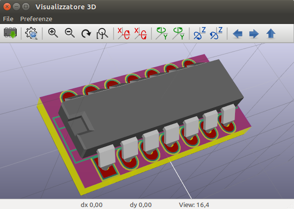
Il visualizzatore 3D è descritto nel manuale dell’editor di circuiti stampati.
Forward and back annotation
Update PCB from Schematic (forward annotation)
Use the Update PCB from Schematic tool to sync design information from the Schematic Editor to the Board Editor. The tool can be accessed with Tools → Update PCB from Schematic (F8) in both the schematic and board editors. You can also use the ![]() icon in the top toolbar of the Board Editor. This process is often called forward annotation.
icon in the top toolbar of the Board Editor. This process is often called forward annotation.
| Update PCB from Schematic is the preferred way to transfer design information from the schematic to the PCB. In older versions of KiCad, the equivalent process was to export a netlist from the Schematic Editor and import it into the Board Editor. It is no longer necessary to use a netlist file. |
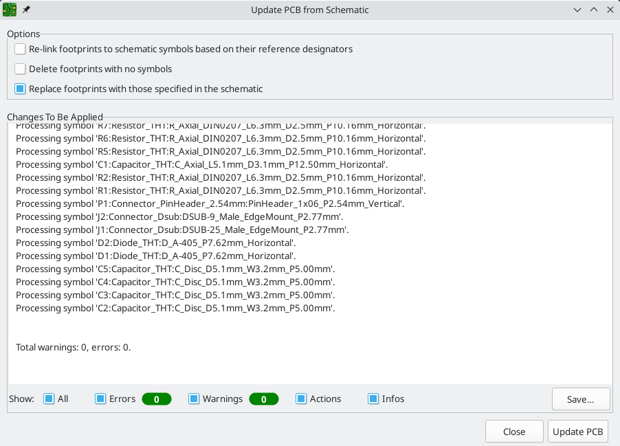
The tool adds the footprint for each symbol to the board and transfers updated schematic information to the board. In particular, the board’s net connections are updated to match the schematic. Symbols with the Exclude from board attribute are not transferred to the PCB.
The changes that will be made to the PCB are listed in the Changes To Be Applied pane. The PCB is not modified until you click the Update PCB button.
You can show or hide different types of messages using the checkboxes at the bottom of the window. A report of the changes can be saved to a file using the Save… button.
Opzioni
The tool has several options to control its behavior.
| Option | Description |
|---|---|
Re-link footprints to schematic symbols based on their reference designators |
Footprints are normally linked to schematic symbols via a unique identifier created when the symbol is added to the schematic. A symbol’s unique identifier cannot be changed. If checked, each footprint in the PCB will be re-linked to the symbol that has the same reference designator as the footprint. If unchecked, footprints and symbols will be linked by unique identifier as usual, rather than by reference designator. Each footprint’s reference designator will be updated to match the reference designator of its linked symbol. This option should generally be left unchecked. It is useful for specific workflows that rely on changing the links between schematic symbols and footprints, such as refactoring a schematic for easier layout or replicating layout between identical channels of a design. |
Delete footprints with no symbols |
If checked, any footprint in the PCB without a corresponding symbol in the schematic will be deleted from the PCB. Footprints with the "Not in schematic" attribute will be unaffected. If unchecked, footprints without a corresponding symbol will not be deleted. |
Replace footprints with those specified in the schematic |
If checked, footprints in the PCB will be replaced with the footprint that is specified in the corresponding schematic symbol. If unchecked, footprints that are already in the PCB will not be changed, even if the schematic symbol is updated to specify a different footprint. |
Update Schematic from PCB (back annotation)
The typical workflow in KiCad is to make changes in the schematic and then sync the changes to the board using the Update PCB From Schematic tool. However, the reverse process is also possible: design changes can be made in the board and then synced back to the schematic using Tools → Update Schematic From PCB in either the schematic or board editors. This process is also known as backannotation.
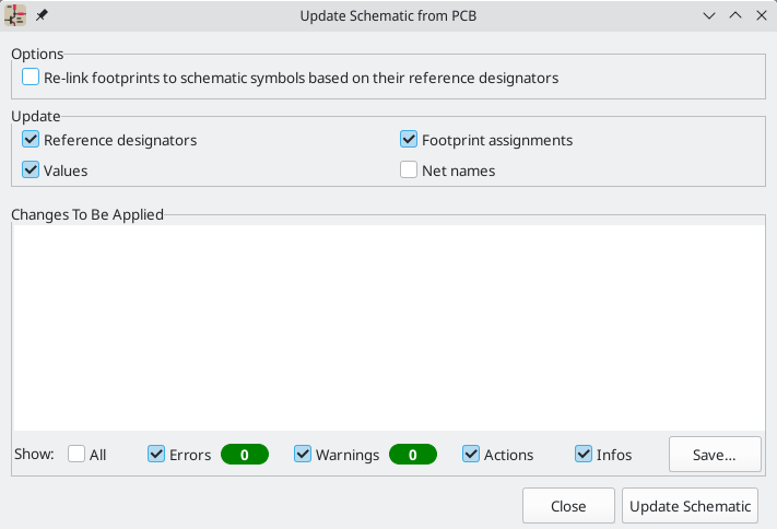
The tool syncs changes in reference designators, values, footprint assignments, and net names from the board to the schematic. Each type of change can be individually enabled or disabled.
The changes that will be made to the schematic are listed in the Changes To Be Applied pane. The schematic is not modified until you click the Update Schematic button.
You can show or hide different types of messages using the checkboxes at the bottom of the window. A report of the changes can be saved to a file using the Save… button.
Opzioni
The tool has several options to control its behavior.
Option |
Description |
Re-link footprints to schematic symbols based on their reference designators |
If checked, each footprint in the PCB will be re-linked to the symbol that has the same reference designator as the footprint. This option is incompatible with updating symbol reference designators. If unchecked, footprints and symbols will be linked by unique identifier as usual, rather than by reference designator. |
Reference designators |
If checked, symbol reference designators will be updated to match the reference designators of the linked footprints. If unchecked, symbol reference designators will not be updated. |
Values |
If checked, symbol values will be updated to match the values of the linked footprints. If unchecked, symbol values will not be updated. |
Footprint assignments |
If checked, footprint assignments will be updated for symbols which have had their footprints changed or replaced in the board. If unchecked, symbol footprint assignments will not be updated. |
Net names |
If checked, the schematic will be updated with any net name changes that have been made in the board. Net labels will be updated or added to the schematic as necessary to match the board. If unchecked, net names will not be updated in the schematic. |
| The Geographical Reannotation feature can be used in combination with backannotating reference designators to reannotate all components in the design based on their location in the layout. |
Back annotation with CMP files
Select changes can also be synced from the PCB back to the schematic by exporting a CMP file from the PCB editor (File → Export → Footprint Association (.cmp) File…) and importing it in the Schematic Editor (File → Import → Footprint Assignments…).
| This method can only sync changes made to footprint assignments and footprint fields. It is recommended to use the Update Schematic from PCB tool instead. |
Generazione risultati
Stampa
KiCad can print the schematic to a standard printer using File→Print….
Opzioni di stampa
Stampa del foglio di disegno: include la stampa del bordo del foglio e del riquadro iscrizioni nella stampa dello schema.
Modalità d’uscita: stampa lo schema a colori o in bianco e nero.
Print background color: Include the background color in the printed schematic. This option is only enabled if Print in black and white only is disabled.
Use a different color theme for printing: Select a different color scheme for printing than the one selected for display in the Schematic Editor.
Page Setup…: Opens a page setup dialog for setting paper size and orientation.
Preview: Opens a print preview dialog.
Close: Closes the dialog without printing.
Print: Opens the system print dialog.
| Printing uses platform- and printer-specific drivers and may have unexpected results. When printing to a file, Plotting is recommended instead of Printing. |
Tracciatura
KiCad can plot schematics to a file using File → Plot….
I formati in uscita supportati sono Postscript, PDF, SVG, DXF e HPGL.
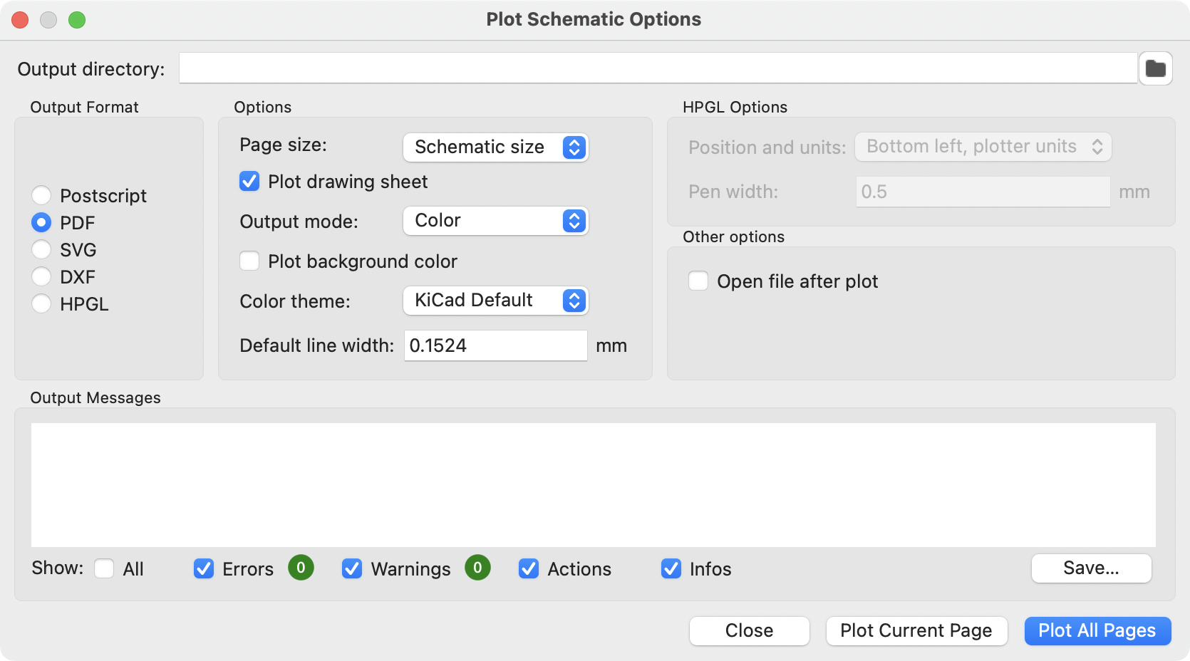
The Output Messages pane displays messages about the generated files. Different kinds of messages can be shown or hidden using the checkboxes, and the messages can be saved to a file using the Save… button.
The Plot Current Page button plots the current page of the schematic. The Plot All Pages button plots all pages of the schematic. One file is generated for each page, except for PDF output, which plots each schematic page as a separate page in a single PDF file.
Opzioni di tracciatura
Output directory: Specify the location to save plotted files. If this is a relative path, it is created relative to the project directory.
Output Format: Select the format to plot in. Some formats have different options than others.
Page size: Sets the page size to use for the plotted output. This can be set to match the schematic size or to another sheet size.
Plot drawing sheet: Include the drawing sheet border and title block in the printed schematic.
Output mode: Sets the output to color or black and white. Not all output formats support color.
Plot background color: Includes the schematic background color in the plotted output. The background color will not be plotted if the output format does not support color or the output mode is black and white.
Color theme: Selects the color theme to use for the plotted output.
Default line width: Selects the default width for lines without a specified thickness (lines that have thickness set to 0). Lines that have a set thickness will be plotted at that thickness instead.
Position and units: Sets the plotter origin and units. This option only applies for HPGL output.
Pen width: Sets the plotter’s pen width. This option only applies for HPGL output.
Open file after plot: automatically opens the plotted output file when plotting is complete.
Caratteristiche dei PDF interattivi
I PDF tracciati hanno diverse caratteristiche interattive.
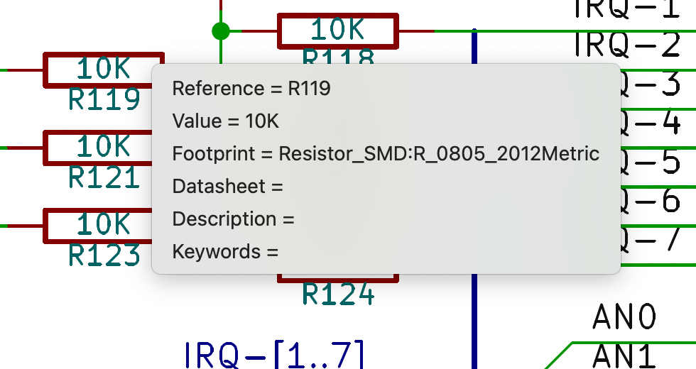
-
I collegamenti ipertestuali funzionano.
-
L’indice viene popolato con fogli schema e con i simboli e le etichette gerarchiche in ogni foglio.
-
Clicking on many schematic elements displays a popup menu containing relevant information.
-
I simboli mostrano i loro campi simbolo.
-
Hierarchical subsheets display their sheetname and filename, as well as an option to enter the sheet itself.
-
Le etichette mostrano i collegamenti e le netclass.
-
I bus mostrano i loro membri.
-
| Alcune di queste caratteristiche non sono supportate in tutti i lettori PDF. |
Generazione della distinta materiali
KiCad can generate a Bill of Materials using Tools → Generate BOM… or the ![]() button on the top toolbar. The generated BOM lists all of the components in the design, except for components with the Exclude from bill of materials property set.
button on the top toolbar. The generated BOM lists all of the components in the design, except for components with the Exclude from bill of materials property set.
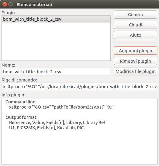
The BOM tool uses an external script to process the design information into the desired output format. Several BOM generator scripts are included with KiCad, and users can also create their own. BOM generator scripts generally use Python or XSLT, but other tools can be used as long as you can specify a command line for KiCad to execute when running the generator.
You can select which BOM generator to use in the BOM generator scripts list. The rest of the dialog displays information about the selected generator. You can change the displayed name of the generator with the Generator nickname textbox.
The pane at right displays information about the selected script. When the generator is executed, the right pane instead displays output from the script.
The text box at the bottom contains the command that KiCad will use to execute the generator. It is automatically populated when a script is selected, but the command may need to be hand-edited for some generators. KiCad saves the command line for each generator when the BOM tool is closed, so command line customizations are preserved. For more details about the command line, see the advanced documentation.
Su MS Windows, la finestra di dialogo del generatore DIBA ha un’opzione aggiuntiva Mostra finestra console che controlla la visibilità della finestra del plugin esterno. Quando questa opzione è deselezionata, i generatori di DIBA vengono eseguiti in una finestra di console nascosta e il risultato viene redirezionato e visualizzato nella finestra di dialogo. Quando questa opzione è selezionata, i generatori di DIBA vengono eseguiti in una finestra di console visibile, che potrebbe essere necessaria se il plugin generatore è fornito di una interfaccia grafica utente.
Script di generazione DIBA
By default, the BOM tool presents three output script options.
-
bom_csv_grouped_extraoutputs a CSV with a single section containing every component in the design. Components are grouped by value, footprint, DNP (do not populate), and any additional fields that are specified on the command line. To specify extra fields, add the desired field names as quoted strings at the end of the command line. For example, to include theMPNfield, the end of the command line would be:<path to script>/bom_csv_grouped_extra.py "%I" "O.csv" "MPN". The columns in the BOM are:-
Line item number
-
Riferimenti
-
Quantità
-
Valore
-
Impronta
-
DNP
-
Specified extra fields
-
-
bom_csv_grouped_by_valueoutputs a CSV with two sections. The first section contains every component in the design, with a single component on each line. The second section also contains every component, but components are grouped by symbol name, value, footprint, and DNP (do not populate). The columns in the BOM are:-
Line item number
-
Quantità
-
Riferimenti
-
Valore
-
Libreria di simboli e nome simbolo
-
Impronta
-
Datasheet
-
DNP
-
Qualsiasi altro campo del simbolo
-
-
bom_csv_grouped_by_value_with_fpoutputs a CSV with a single section containing every component in the design. Components are grouped by value, footprint, and DNP (do not populate). The columns in the BOM are:-
Riferimenti
-
Quantità
-
Valore
-
Nome simbolo
-
Impronta
-
Descrizione simbolo
-
Marchio
-
DNP
-
Additional generator scripts are installed with KiCad but are not populated in the generator script list by default. The location of these scripts depends on the operating system and may vary based on installation location.
| Operating System | Location |
|---|---|
Windows |
|
Linux |
|
macOS |
|
Ulteriori script possono essere aggiunti all’elenco degli script del generatore DIBA facendo clic sul pulsante ![]() . Gli script possono essere rimossi facendo clic sul pulsante
. Gli script possono essere rimossi facendo clic sul pulsante ![]() . Il pulsante
. Il pulsante ![]() apre lo script selezionato in un editor di testo.
apre lo script selezionato in un editor di testo.
For more information on creating and using custom BOM generators, see the advanced documentation.
Altri modi per generare una DIBA
KiCad offers several additional ways to generate a BOM, although the BOM tool is recommended.
-
The Symbol Fields Table can export a CSV which can be used as a BOM. This option includes all symbol information but offers limited control over the output.
-
The PCB Editor can export a BOM through File → Fabrication Outputs → BOM…. This method provides no control over the output format and does not include all symbol information.
Generazione di una netlist
Una netlist è un file che descrive le connessioni elettriche tra i pin dei simboli. Queste connessioni sono chiamate net o collegamenti. I file netlist contengono:
-
Un elenco di simboli e dei loro pin.
-
L’elenco delle connessioni (net) tra pin di simboli.
Esistono diversi formati di netlist. A volte, l’elenco simboli e l’elenco dei collegamenti, sono due file separati. La netlist è fondamentale per uso di software di progettazione elettronica, dato che la netlist è anche un mezzo di collegamento con gli altri software di CAD elettronico, come software di progettazione circuiti stampati, simulatori e compilatori di logiche programmabili.
KiCad supporta diversi formati di netlist:
-
KiCad format, which can be imported by the KiCad PCB Editor. However, the "Update PCB from Schematic" tool should be used instead of importing a KiCad netlist into the PCB editor.
-
Formato OrCAD PCB2, per progettare circuiti stampati con OrCAD.
-
Formato CADSTAR, per progettare circuiti stampati con CADSTAR.
-
Formato Spice, per l’uso di vari simulatori esterni di circuiti elettronici.
| In KiCad version 5.0 and later, it is not necessary to create a netlist for transferring a design from the schematic editor to the PCB editor. Instead, use the "Update PCB from Schematic" tool. |
| Other software tools that use netlists may have restrictions on spaces and special characters in component names, pins, nets, and other fields. For compatibility, be aware of such restrictions in other tools you plan to use, and name components, nets, etc. accordingly. |
Formati di netlist
Netlists are exported with the Export Netlist dialog (File→Export→Netlist…).
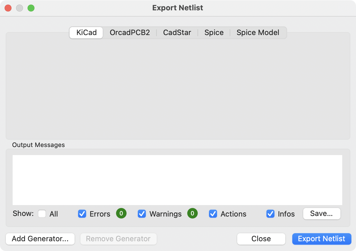
KiCad supports exporting netlists in several formats: KiCad, OrcadPCB2, CADSTAR, Spice, and Spice Model. Each format can be selected by selecting the corresponding tab at the top of the window. Some netlist formats have additional options.
Clicking the Export Netlist button prompts for a netlist filename and saves the netlist.
| La generazione della netlist può impiegare diversi minuti con schemi elettrici estesi. |
Custom generators for other netlist formats can be added by clicking the Add Generator… button. Custom generators are external tools that are called by KiCad, for example Python scripts or XSLT stylesheets. For more information on custom netlist generators, see the section on adding custom netlist generators.
Formati netlist Spice
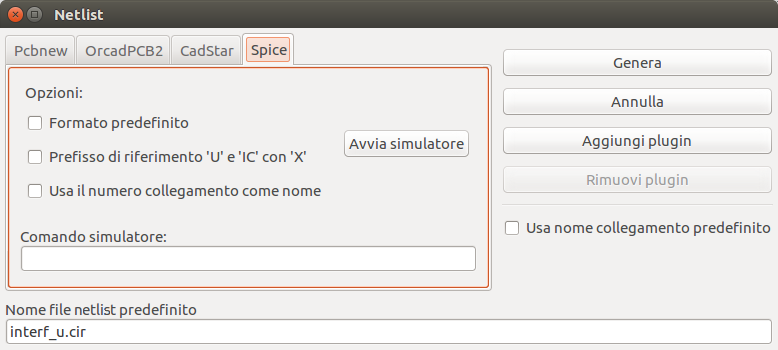
Il formato netlist Spice offre diverse opzioni.
When the use current sheet as root is selected, only the current sheet is exported to a subcircuit model. Otherwise, the entire schematic sheet is exported.
The save all voltages option adds a .save all command to the netlist, which causes the simulator to save all node voltages. The save all currents option adds a .probe alli command to the netlist, which causes the simulator save all node currents.
| Exact behavior may vary between simulation tools. |
Passive symbol values are automatically adjusted to be compatible with various Spice simulators. Specifically:
-
μandMas unit prefixes are replaced withuandMeg, respectively -
Units are removed (e.g.
4.7kΩis changed to4.7k) -
Values in RKM format are rewritten to be Spice-compatible (e.g.
4u7is changed to4.7u)
The Spice netlist exporter also provides an easy way to simulate the generated netlist with an external simulator. This can be useful for running a simulation without using KiCad’s internal ngspice simulator, or for running an ngspice simulation with options that are not supported by KiCad’s simulator tool.
Enter the path to the external simulator in the text box, with %I representing the generated netlist. Click the Create Netlist and Run Simulator Command button to generate the netlist and automatically run the simulator.
The default simulator command (spice "%I") must be adjusted to point to
a simulator installed on your system.
|
Spice simulators expect simulation commands (.PROBE, .AC, .TRAN, etc.) to be included in the netlist. Any text line included in the schematic diagram starting with a period (.) will be included in the netlist. If a text object contains multiple lines, only the lines beginning with a period will be included.
.include directives for including model library files are automatically added to the netlist based on the Spice model settings for the symbols in the schematic.
Formati netlist modelli Spice
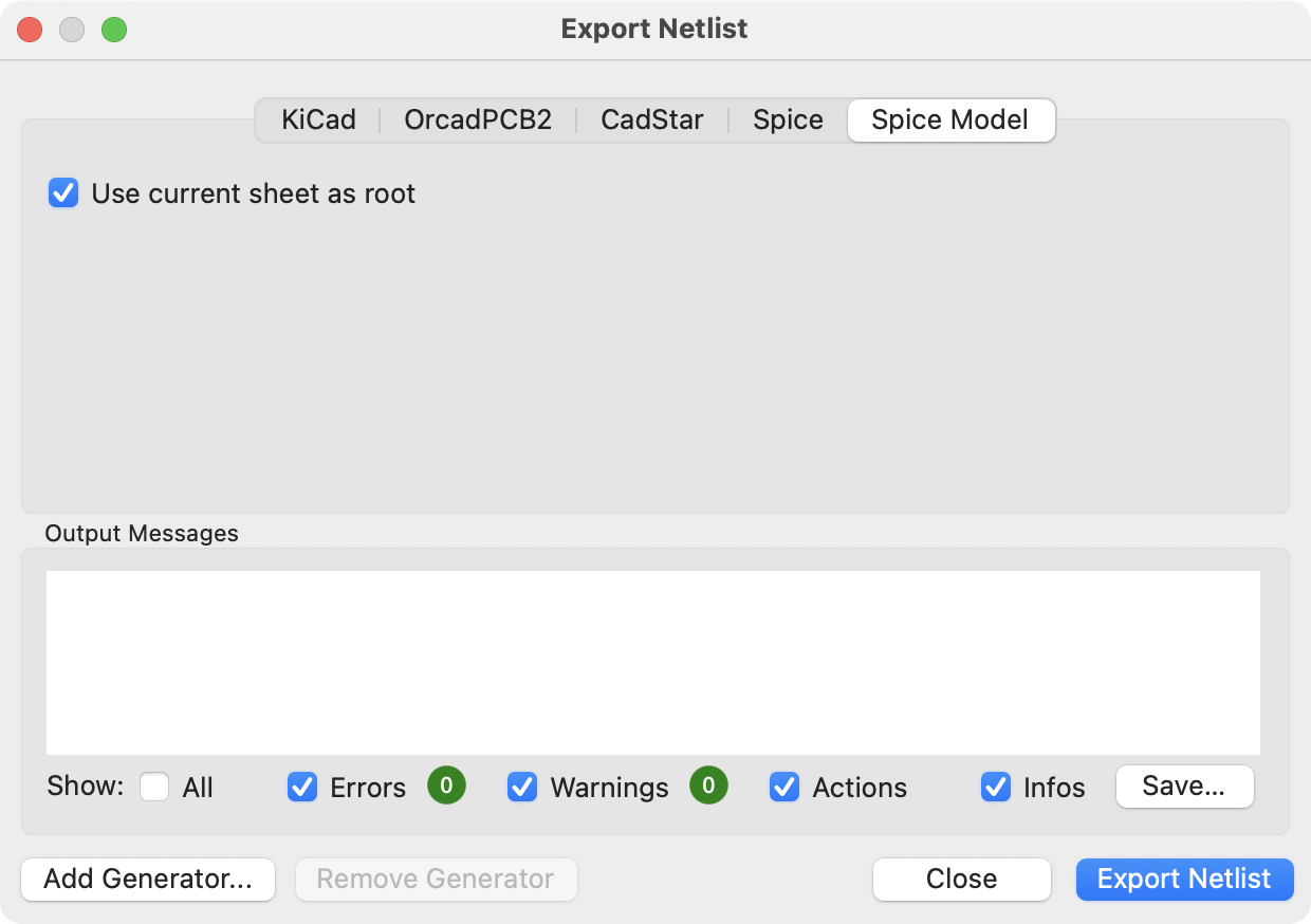
KiCad can also export a netlist of the schematic as a Spice subcircuit model, which can be included in a separate Spice simulation. Any hierarchical labels in the schematic are used as pins for the subcircuit model. Each pin in the model is annotated with a comment describing the pin’s electrical direction:
-
Inputhierarchical labels are mapped to aninputannotation -
Outputhierarchical labels are mapped to anoutputannotation -
Bidirectionalhierarchical labels are mapped to aninoutannotation -
Tri-statehierarchical labels are mapped to atristateannotation -
Passivehierarchical labels are mapped to apassiveannotation
When the use current sheet as root is selected, only the current sheet is exported to a subcircuit model. Otherwise, the entire schematic sheet is exported.
Esempi netlist
Below is the schematic from the sallen_key project included in KiCad’s simulation demos.
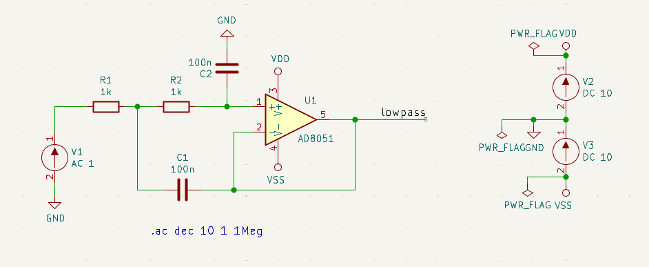
La netlist in formato KiCad per questo schema è la seguente:
(export (version "E")
  (design
    (source "/usr/share/kicad/demos/simulation/sallen_key/sallen_key.kicad_sch")
    (date "Sun 01 May 2022 03:14:05 PM EDT")
    (tool "Eeschema (6.0.4)")
    (sheet (number "1") (name "/") (tstamps "/")
      (title_block
        (title)
        (company)
        (rev)
        (date)
        (source "sallen_key.kicad_sch")
        (comment (number "1") (value ""))
        (comment (number "2") (value ""))
        (comment (number "3") (value ""))
        (comment (number "4") (value ""))
        (comment (number "5") (value ""))
        (comment (number "6") (value ""))
        (comment (number "7") (value ""))
        (comment (number "8") (value ""))
        (comment (number "9") (value "")))))
  (components
    (comp (ref "C1")
      (value "100n")
      (libsource (lib "sallen_key_schlib") (part "C") (description ""))
      (property (name "Sheetname") (value ""))
      (property (name "Sheetfile") (value "sallen_key.kicad_sch"))
      (sheetpath (names "/") (tstamps "/"))
      (tstamps "00000000-0000-0000-0000-00005789077d"))
    (comp (ref "C2")
      (value "100n")
      (fields
        (field (name "Fieldname") "Value")
        (field (name "SpiceMapping") "1 2")
        (field (name "Spice_Primitive") "C"))
      (libsource (lib "sallen_key_schlib") (part "C") (description ""))
      (property (name "Fieldname") (value "Value"))
      (property (name "Spice_Primitive") (value "C"))
      (property (name "SpiceMapping") (value "1 2"))
      (property (name "Sheetname") (value ""))
      (property (name "Sheetfile") (value "sallen_key.kicad_sch"))
      (sheetpath (names "/") (tstamps "/"))
      (tstamps "00000000-0000-0000-0000-00005789085b"))
    (comp (ref "R1")
      (value "1k")
      (fields
        (field (name "Fieldname") "Value")
        (field (name "SpiceMapping") "1 2")
        (field (name "Spice_Primitive") "R"))
      (libsource (lib "sallen_key_schlib") (part "R") (description ""))
      (property (name "Fieldname") (value "Value"))
      (property (name "SpiceMapping") (value "1 2"))
      (property (name "Spice_Primitive") (value "R"))
      (property (name "Sheetname") (value ""))
      (property (name "Sheetfile") (value "sallen_key.kicad_sch"))
      (sheetpath (names "/") (tstamps "/"))
      (tstamps "00000000-0000-0000-0000-0000578906ff"))
    (comp (ref "R2")
      (value "1k")
      (fields
        (field (name "Fieldname") "Value")
        (field (name "SpiceMapping") "1 2")
        (field (name "Spice_Primitive") "R"))
      (libsource (lib "sallen_key_schlib") (part "R") (description ""))
      (property (name "Fieldname") (value "Value"))
      (property (name "SpiceMapping") (value "1 2"))
      (property (name "Spice_Primitive") (value "R"))
      (property (name "Sheetname") (value ""))
      (property (name "Sheetfile") (value "sallen_key.kicad_sch"))
      (sheetpath (names "/") (tstamps "/"))
      (tstamps "00000000-0000-0000-0000-000057890691"))
    (comp (ref "U1")
      (value "AD8051")
      (fields
        (field (name "Spice_Lib_File") "ad8051.lib")
        (field (name "Spice_Model") "AD8051")
        (field (name "Spice_Netlist_Enabled") "Y")
        (field (name "Spice_Primitive") "X"))
      (libsource (lib "sallen_key_schlib") (part "Generic_Opamp") (description ""))
      (property (name "Spice_Primitive") (value "X"))
      (property (name "Spice_Model") (value "AD8051"))
      (property (name "Spice_Lib_File") (value "ad8051.lib"))
      (property (name "Spice_Netlist_Enabled") (value "Y"))
      (property (name "Sheetname") (value ""))
      (property (name "Sheetfile") (value "sallen_key.kicad_sch"))
      (sheetpath (names "/") (tstamps "/"))
      (tstamps "00000000-0000-0000-0000-00005788ff9f"))
    (comp (ref "V1")
      (value "AC 1")
      (libsource (lib "sallen_key_schlib") (part "VSOURCE") (description ""))
      (property (name "Sheetname") (value ""))
      (property (name "Sheetfile") (value "sallen_key.kicad_sch"))
      (sheetpath (names "/") (tstamps "/"))
      (tstamps "00000000-0000-0000-0000-000057336052"))
    (comp (ref "V2")
      (value "DC 10")
      (fields
        (field (name "Fieldname") "Value")
        (field (name "Spice_Node_Sequence") "1 2")
        (field (name "Spice_Primitive") "V"))
      (libsource (lib "sallen_key_schlib") (part "VSOURCE") (description ""))
      (property (name "Fieldname") (value "Value"))
      (property (name "Spice_Primitive") (value "V"))
      (property (name "Spice_Node_Sequence") (value "1 2"))
      (property (name "Sheetname") (value ""))
      (property (name "Sheetfile") (value "sallen_key.kicad_sch"))
      (sheetpath (names "/") (tstamps "/"))
      (tstamps "00000000-0000-0000-0000-0000578900ba"))
    (comp (ref "V3")
      (value "DC 10")
      (fields
        (field (name "Fieldname") "Value")
        (field (name "Spice_Node_Sequence") "1 2")
        (field (name "Spice_Primitive") "V"))
      (libsource (lib "sallen_key_schlib") (part "VSOURCE") (description ""))
      (property (name "Fieldname") (value "Value"))
      (property (name "Spice_Primitive") (value "V"))
      (property (name "Spice_Node_Sequence") (value "1 2"))
      (property (name "Sheetname") (value ""))
      (property (name "Sheetfile") (value "sallen_key.kicad_sch"))
      (sheetpath (names "/") (tstamps "/"))
      (tstamps "00000000-0000-0000-0000-000057890232")))
  (libparts
    (libpart (lib "sallen_key_schlib") (part "C")
      (footprints
        (fp "C?")
        (fp "C_????_*")
        (fp "C_????")
        (fp "SMD*_c")
        (fp "Capacitor*"))
      (fields
        (field (name "Reference") "C")
        (field (name "Value") "C"))
      (pins
        (pin (num "1") (name "") (type "passive"))
        (pin (num "2") (name "") (type "passive"))))
    (libpart (lib "sallen_key_schlib") (part "Generic_Opamp")
      (fields
        (field (name "Reference") "U")
        (field (name "Value") "Generic_Opamp"))
      (pins
        (pin (num "1") (name "+") (type "input"))
        (pin (num "2") (name "-") (type "input"))
        (pin (num "3") (name "V+") (type "power_in"))
        (pin (num "4") (name "V-") (type "power_in"))
        (pin (num "5") (name "") (type "output"))))
    (libpart (lib "sallen_key_schlib") (part "R")
      (footprints
        (fp "R_*")
        (fp "Resistor_*"))
      (fields
        (field (name "Reference") "R")
        (field (name "Value") "R"))
      (pins
        (pin (num "1") (name "") (type "passive"))
        (pin (num "2") (name "") (type "passive"))))
    (libpart (lib "sallen_key_schlib") (part "VSOURCE")
      (fields
        (field (name "Reference") "V")
        (field (name "Value") "VSOURCE")
        (field (name "Fieldname") "Value")
        (field (name "Spice_Primitive") "V")
        (field (name "Spice_Node_Sequence") "1 2"))
      (pins
        (pin (num "1") (name "") (type "input"))
        (pin (num "2") (name "") (type "input")))))
  (libraries
    (library (logical "sallen_key_schlib")
      (uri "/usr/share/kicad/demos/simulation/sallen_key/sallen_key_schlib.kicad_sym")))
  (nets
    (net (code "1") (name "/lowpass")
      (node (ref "C1") (pin "1") (pintype "passive"))
      (node (ref "U1") (pin "2") (pinfunction "-") (pintype "input"))
      (node (ref "U1") (pin "5") (pintype "output")))
    (net (code "2") (name "GND")
      (node (ref "C2") (pin "2") (pintype "passive"))
      (node (ref "V1") (pin "2") (pintype "input"))
      (node (ref "V2") (pin "2") (pintype "input"))
      (node (ref "V3") (pin "1") (pintype "input")))
    (net (code "3") (name "Net-(C1-Pad2)")
      (node (ref "C1") (pin "2") (pintype "passive"))
      (node (ref "R1") (pin "1") (pintype "passive"))
      (node (ref "R2") (pin "2") (pintype "passive")))
    (net (code "4") (name "Net-(C2-Pad1)")
      (node (ref "C2") (pin "1") (pintype "passive"))
      (node (ref "R2") (pin "1") (pintype "passive"))
      (node (ref "U1") (pin "1") (pinfunction "+") (pintype "input")))
    (net (code "5") (name "Net-(R1-Pad2)")
      (node (ref "R1") (pin "2") (pintype "passive"))
      (node (ref "V1") (pin "1") (pintype "input")))
    (net (code "6") (name "VDD")
      (node (ref "U1") (pin "3") (pinfunction "V+") (pintype "power_in"))
      (node (ref "V2") (pin "1") (pintype "input")))
    (net (code "7") (name "VSS")
      (node (ref "U1") (pin "4") (pinfunction "V-") (pintype "power_in"))
      (node (ref "V3") (pin "2") (pintype "input")))))
In formato Spice, la netlist è la seguente:
.title KiCad schematic
.include "ad8051.lib"
XU1 Net-_C2-Pad1_ /lowpass VDD VSS /lowpass AD8051
C2 Net-_C2-Pad1_ GND 100n
C1 /lowpass Net-_C1-Pad2_ 100n
R2 Net-_C2-Pad1_ Net-_C1-Pad2_ 1k
R1 Net-_C1-Pad2_ Net-_R1-Pad2_ 1k
V1 Net-_R1-Pad2_ GND AC 1
V2 VDD GND DC 10
V3 GND VSS DC 10
.ac dec 10 1 1Meg
.end
Symbols and Symbol Libraries
KiCad organizes symbols into symbol libraries, which hold collections of symbols. Each symbol in a schematic is uniquely identified by a full name that is composed of a library nickname and a symbol name. For example, the identifier Audio:AD1853 refers to the AD1853 symbol in the Audio library.
Managing symbol libraries
KiCad uses a table of symbol libraries to map a symbol library nickname to an underlying symbol library on disk. Kicad uses a global symbol library table as well as a table specific to each project. To edit either symbol library table, use Preferences → Manage Symbol Libraries….
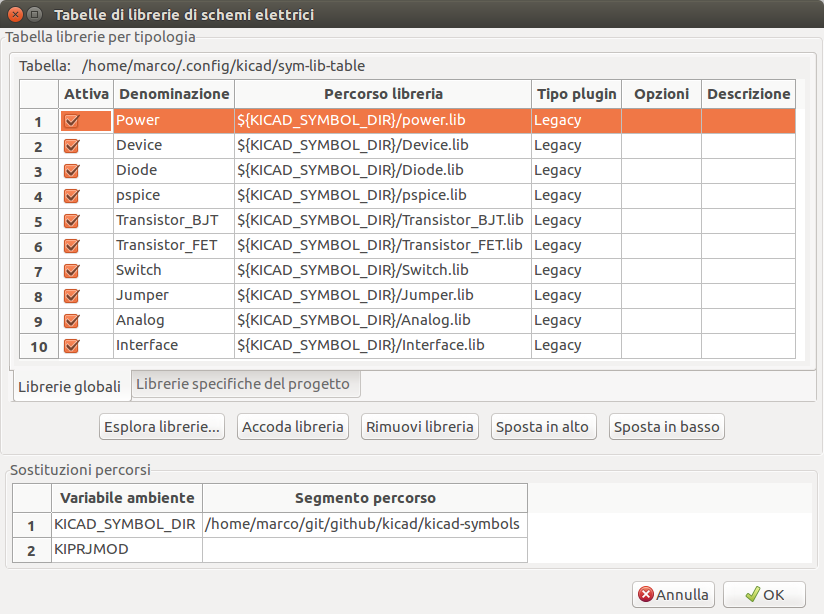
La tabella delle librerie simboli globali contiene l’elenco delle librerie sempre disponibili indipendentemente dal progetto attualmente caricato. La tabella viene salvata nel file sym-lib-table nella cartella di configurazione di KiCad. La posizione di questa cartella dipende dal sistema operativo utilizzato.
La tabella della libreria dei simboli specifica del progetto contiene l’elenco delle librerie che sono disponibili specificamente per il progetto attualmente caricato. Se sono presenti librerie di simboli specifiche del progetto, la tabella viene salvata nel file sym-lib-table nella cartella del progetto.
Configurazione iniziale
The first time the KiCad Schematic Editor is run and the global symbol table file sym-lib-table is not found in the KiCad configuration folder, KiCad will guide the user through setting up a new symbol library table. This process is described above.
Gestione voci della tabella
Symbol libraries can only be used if they have been added to either the global or project-specific symbol library table.
Aggiungere una libreria facendo clic sul pulsante ![]() selezionando una libreria o facendo clic sul pulsante
selezionando una libreria o facendo clic sul pulsante ![]() e digitando il percorso di un file di libreria . La libreria selezionata verrà aggiunta alla tabella della libreria attualmente aperta (globale o specifica del progetto). Le librerie possono venir rimosse selezionando le voci della libreria desiderate e facendo clic sul pulsante
e digitando il percorso di un file di libreria . La libreria selezionata verrà aggiunta alla tabella della libreria attualmente aperta (globale o specifica del progetto). Le librerie possono venir rimosse selezionando le voci della libreria desiderate e facendo clic sul pulsante ![]() .
.
The ![]() and
and ![]() buttons move the selected library up and down in the library table. This does not affect the display order of libraries in the Symbol Library Browser, Symbol Editor, or Add Symbol tool.
buttons move the selected library up and down in the library table. This does not affect the display order of libraries in the Symbol Library Browser, Symbol Editor, or Add Symbol tool.
Libraries can be made inactive by unchecking the Active checkbox in the first column. Inactive libraries are still in the library table but do not appear in any library browsers and are not loaded from disk, which can reduce loading times.
A range of libraries can be selected by clicking the first library in the range and then Shift-clicking the last library in the range.
Each library must have a unique nickname: duplicate library nicknames are not allowed in the same table. However, nicknames can be duplicated between the global and project library tables. Libraries in the project table take precedence over libraries with the same name in the global table.
Gli identificatori di libreria non devono essere correlati al nome file o al percorso della libreria. Il carattere due punti (:) non può essere utilizzato negli identificatori di libreria o nei nomi dei simboli perché viene utilizzato come separatore tra identificatori e simboli.
Each library entry must have a valid path. Paths can be defined as absolute, relative, or by environment variable substitution.
The appropriate library format must be selected in order for the library to be properly read. "KiCad" format is used for KiCad version 6+ libraries (.kicad_sym files), while "Legacy" format is used for libraries from older versions of KiCad (.lib files). Legacy libraries are read-only, but can be migrated to KiCad format libraries using the Migrate Libraries button (see section Migrating Legacy Libraries).
Esiste un campo optionale per la descrizione della voce di libreria. Il campo opzioni non viene usato al momento perciò aggiungere opzioni non ha alcun effetto sul caricamento delle librerie.
Sostituzione delle variabili ambiente
Le tabelle delle librerie di simboli supportano la sostituzione delle variabili ambiente, che consente di definire variabili ambiente contenenti percorsi personalizzati in cui sono archiviate le librerie. La sostituzione delle variabili ambiente è supportata usando la sintassi ${ENV_VAR_NAME} nel percorso della libreria dei simboli.
By default, KiCad defines several environment variables which are described in the project manager documentation. Environment variables can be configured in the Preferences → Configure Paths… dialog.
Using environment variables in the symbol library tables allows libraries to be relocated without breaking the symbol library tables, so long as the environment variables are updated when the library location changes.
${KIPRJMOD} is a special environment variable that always expands to the absolute path of the current project directory. ${KIPRJMOD} allows libraries to be stored in the project folder without having to use an absolute path in the project library table. This makes it possible to relocate projects without breaking their project library tables.
Modelli di utilizzo
Le librerie di simboli si possono definire sia globalmente che specificatamente al progetto correntemente caricato. Le librerie di simboli definite nella tabella globale dell’utente sono sempre disponibili e vengono memorizzate nel file sym-lib-table nella cartella di configurazione di KiCad dell’utente. La tabella delle librerie di simboli specifica del progetto è attiva solamente per il file progetto aperto al momento.
Ci sono vantaggi e svantaggi per ogni metodo. Definire tutte le librerie nella tabella globale significa che queste saranno sempre disponibili alla bisogna. Lo svantaggio di ciò è aumenterà che il tempo di caricamento.
Definire tutte le librerie di simboli su base specifica del progetto significa che si avranno solamente le librerie necessarie per quel progetto e ciò diminuirà il tempo di caricamento dei simboli. Lo svantaggio è che sarà sempre necessario ricordarsi di aggiungere ogni libreria di simboli necessaria per ogni progetto.
Uno schema di utilizzo potrebbe essere quello di definire le librerie di uso comune a livello globale e le librerie richieste solo per il progetto nella tabella della libreria specifica del progetto.
Migrazione delle librerie obsolete
Legacy libraries (.lib files) are read-only, but they can be migrated to KiCad version 6 libraries (.kicad_sym). KiCad version 6 libraries cannot be viewed or edited by KiCad versions older than 6.0.0.
Legacy libraries can be converted to KiCad 6 libraries by selecting them in the symbol library table and clicking the Migrate Libraries button. Multiple libraries can be selected and migrated at once by Ctrl-clicking or shift-clicking.
Libraries can also be converted one at a time by opening them in the Symbol Editor and saving them as a new library.
Rimappatura dei vecchi progetti
Quando si carica uno schema creato prima dell’implementazione della tabella delle librerie di simboli, KiCad cercherà di rimappare i collegamenti alle librerie di simboli presenti nello schema ai simboli nella tabella librerie appropriati. Il successo di questo processo dipende da diversi fattori:
-
le librerie originali usate nello schema sono ancora disponibili e invariate da quando il simbolo è stato aggiunto allo schema.
-
tutte le operazioni di salvataggio sono state eseguite quando sono state rilevate per creare una libreria di salvataggio o mantenere aggiornata la libreria di salvataggio esistente.
-
l’integrità della libreria cache dei simboli del progetto non è stata danneggiata.
|
La rimappatura eseguirà un salvataggio di tutti i file che vengono modificati durante l’operazione, nella cartella di salvataggio all’interno della cartella del progetto. Effettuare sempre un salvataggio del progetto prima di rimappare, (N.d.T. per evitare brutte sorprese) nel caso in cui qualcosa vada storto. |
|
L’operazione di recupero viene eseguita anche se è stata disabilitata per garantire che i simboli corretti siano disponibili per la rimappatura. Non annullare questa operazione o la rimappatura non riuscirà a rimappare correttamente i simboli degli schemi. Eventuali collegamenti a simboli spezzati dovranno essere corretti manualmente. |
|
Se le librerie originali sono state rimosse e il recupero non è stato eseguito, la cache della libreria può essere utilizzata come libreria di ripristino come ultima risorsa. Copiare la libreria della cache in un nuovo nome file e aggiungere il nuovo file della libreria all’inizio dell’elenco delle librerie usando una versione di KiCad precedente all’implementazione della tabella della libreria dei simboli. |
Creating and editing symbols
Overview of symbols and symbol libraries
A symbol is a schematic representation of a component. A symbol is composed of:
-
Elementi grafici (linee, cerchi, archi, testo, ecc.) che determinano l’aspetto del simbolo nello schema elettrico.
-
Pins, which have both graphic properties (line, clock, inverted, low level active, etc.) and electrical properties (input, output, bidirectional, etc.) used by the Electrical Rules Check (ERC) tool.
-
Fields, such as references, values, corresponding footprint names for PCB design, etc.
Una libreria di simboli è composta da uno o più simboli. Generalmente i simboli sono raggruppati per funzione, tipo e/o produttore.
I simboli possono essere derivati da un altro simbolo nella stessa libreria. I simboli derivati condividono la forma grafica e le definizioni dei pin del simbolo di base, ma possono sovrascrivere i campi delle proprietà del simbolo di base (valore, impronta, filtri impronta, documentazione, descrizione, ecc.). I simboli derivati possono essere utilizzati per definire simboli simili ad una parte di base. Ad esempio, i simboli 74LS00, 74HC00 e 7437 potrebbero essere tutti derivati da un simbolo 7400. Nelle versioni precedenti di KiCad, i simboli derivati erano chiamati alias.
Symbol Editor overview
KiCad provides a symbol editing tool that allows you to create libraries, add, delete or transfer symbols between libraries, export symbols to files, and import symbols from files.
In general, the flow for designing a symbol involves:
-
Specificare se il simbolo è formato da più di un’unità.
-
Specificare se il simbolo possiede uno stile corpo alternativo (altrimenti detto rappresentazione De Morgan).
-
La progettazione della sua rappresentazione simbolica usando linee, rettangoli, cerchi, poligoni e testo.
-
Adding pins by carefully defining each pin’s graphical elements, name, number, and electrical property (input, output, tri-state, power output, etc.).
-
Determining if the symbol should be derived from another symbol with the same graphical design and pin definition.
-
L’aggiunta di campi opzionali come il nome dell’impronta usata dal software di progettazione di circuiti stampati e/o la definizione della loro visibilità.
-
La documentazione del simbolo aggiungendo una stringa di descrizione, collegamenti ai datasheet, ecc.
-
Il salvataggio nella libreria scelta.
The Symbol Editor main window is shown below. It consists of three toolbars for quick access to common features and a symbol viewing/editing area. Not all commands are available on the toolbars, but all commands are available in the menus.
Barra strumenti principale
The main toolbar is at the top of the main window. It has buttons for the undo/redo commands, zoom commands, symbol properties dialogs, and unit/representation management controls.
|
Create a new symbol in the selected library. |
|
Save the currently selected library. All modified symbols in the library will be saved. |
|
Undo last edit. |
|
Redo last undo. |
|
Refresh display. |
|
Zoom in. |
|
Zoom out. |
|
Zoom to fit symbol in display. |
|
Zoom to fit selection. |
|
Rotate counter-clockwise. |
|
Rotate clockwise. |
|
Mirror horizontally. |
|
Mirror vertically. |
|
Edit the current symbol properties. |
|
Edit the symbol’s pins in a tabular interface. |
|
Open the symbol’s datasheet, if it is defined. |
|
Test the current symbol for design errors. |
|
Select the normal body style. The button is disabled if the current symbol does not have an alternate body style. |
|
Select the alternate body style. The button is disabled if the current symbol does not have an alternate body style. |
|
Select the unit of a multi-unit symbol to display. The drop down control will be disabled if the current symbol is not derived from a symbol with multiple units. |
|
Enable synchronized pins edit mode. When this mode is enabled, any pin modifications are propagated to all other symbol units. Pin number changes are not propagated. This mode is automatically enabled for symbols with multiple interchangeable units and cannot be enabled for symbols with only one unit. |
|
Insert current symbol into the schematic. |
Barra strumenti elementi
La barra strumenti verticale sul lato destro della finestra principale permette di piazzare tutti gli elementi richiesti per progettare un simbolo.
|
Select tool. Right-clicking with the select tool opens the context menu for the object under the cursor. Left-clicking with the select tool displays the attributes of the object under the cursor in the message panel at the bottom of the main window. Double-left-clicking with the select tool will open the properties dialog for the object under the cursor. |
|
Pin tool. Left-click to add a new pin. |
|
Graphical text tool. Left-click to add a new graphical text item. |
|
Graphical textbox tool. Left-click to add a new graphical textbox item. |
|
Rectangle tool. Left-click to begin drawing the first corner of a graphical rectangle. Left-click again to place the opposite corner of the rectangle. |
|
Circle tool. Left-click to begin drawing a new graphical circle from the center. Left-click again to define the radius of the circle. |
|
Arc tool. Left-click to begin drawing a new graphical arc item from the first arc end point. Left-click again to define the second arc end point. Adjust the radius by dragging the arc center point. |
|
Connected line tool. Left-click to begin drawing a new graphical line item in the current symbol. Left-click for each additional connected line. Double-left-click to complete the line. |
|
Anchor tool. Left-click to set the anchor position of the symbol. |
|
Delete tool. Left-click to delete an object from the current symbol. |
Barra opzioni
La barra strumenti verticale, posizionata sul lato sinistro della finestra principale, permette di impostare alcune opzioni di disegno dell’editor.
|
Toggle grid visibility on and off. |
|
Set units to inches. |
|
Set units to mils (0.001 inch). |
|
Set units to millimeters. |
|
Toggle full screen cursor on and off. |
|
Toggle display of pin electrical types. |
|
Toggle display of library and symbol tree. |
Saving symbols to libraries
The ![]() button displays or hides the list of available libraries, which allows you to select an active library. When a symbol is saved, it will be placed in this library.
button displays or hides the list of available libraries, which allows you to select an active library. When a symbol is saved, it will be placed in this library.
Clicking the ![]() icon on the left toolbar toggles the treeview of libraries and symbols. Clicking on a symbol opens that symbol.
icon on the left toolbar toggles the treeview of libraries and symbols. Clicking on a symbol opens that symbol.
| Alcuni simboli sono derivati da altri simboli. I nomi dei simboli derivati vengono visualizzati in corsivo nella vista ad albero. Se un simbolo derivato viene aperto, la sua grafica non sarà modificabile. I suoi campi simbolo invece saranno modificabili normalmente. Per modificare la grafica di un simbolo base e di tutti i suoi simboli derivati, bisogna aprire il simbolo base. |
Dopo la modifica, un simbolo può essere salvato nella libreria corrente o in una nuova libreria.
Per salvare il simbolo modificato nella libreria corrente, fare clic sull’icona ![]() . Le modifiche verranno scritte sul simbolo esistente.
. Le modifiche verranno scritte sul simbolo esistente.
| Saving a modified symbol also saves all other modified symbols in the same library. |
Per salvare i cambiamenti del simbolo in un nuovo simbolo, fare clic su File → Salva con nome…. Il simbolo può essere salvato nella libreria corrente o in una diversa libreria. Si può impostare anche un nuovo nome per il simbolo.
Per creare un nuovo file contenente solo il simbolo corrente, fare clic su File → Esporta → Simbolo…. Questo file sarà un file di libreria standard che conterrà solo un simbolo.
Creating symbols
Creating a new symbol
Un nuovo simbolo può essere creato facendo clic sull’icona ![]() . Verranno richieste un certo numero di proprietà del simbolo.
. Verranno richieste un certo numero di proprietà del simbolo.
-
A symbol name
-
An optional base symbol to derive the new symbol from. The new symbol will use the base symbol’s graphical shape and pin configuration, but other symbol information can be modified in the derived symbol. The base symbol must be in the same library as the new derived symbol.
-
Il prefisso del riferimento (
U,C,R…). -
The number of units per package, and whether those units are interchangeable (for example a 7400 quad NAND symbol could have 4 units, one for each gate).
-
If an alternate body style (sometimes referred to as a "De Morgan equivalent") is desired.
-
Whether the symbol is a power symbol. Power symbols appear in the Add Power Symbol dialog in the Schematic editor, their
Valuefields are not editable in the schematic, they cannot be assigned a footprint, they are not added to the PCB, and they are not included in the bill of materials. -
Whether the symbol should be excluded from the bill of materials.
-
Whether the symbol should be excluded from the PCB.
There are also several graphical options.
-
The offset between the end of each pin and its pin name.
-
Whether the pin number and pin name should be displayed.
-
Whether the pin names should be displayed alongside the pins or at the ends of the pins inside the symbol body.
These properties can also be changed later in the Symbol Properties window.
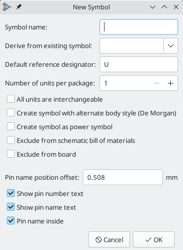
Un nuovo simbolo verrà creato usando le proprietà sopraesposte e apparirà nell’editor come mostrato sotto.
The blue cross in the center is the symbol anchor, which specifies the symbol origin i.e. the coordinates (0, 0). The anchor can be repositioned by selecting the ![]() icon and clicking on the new desired anchor position.
icon and clicking on the new desired anchor position.
Creating a symbol from another symbol
Spesso, il simbolo che si vuole creare è simile ad un altro già presente in una libreria componenti. In questo caso risulta più facile caricare e modificare un simbolo esistente (N.d.T. piuttosto che ricrearne uno nuovo da zero).
-
Caricare il simbolo che verrà usato come punto di partenza.
-
Save a new copy of the symbol using File → Save As…. The Save As dialog will prompt for a name for the new symbol and the library to save it in.
-
Modifica il nuovo simbolo come richiesto.
-
Salva il simbolo modificato.
Proprietà del simbolo
Symbol properties are set when the symbol is created but they can be modified at any point. To change the symbol properties, click on the ![]() button to show the Symbol Properties dialog. You can also double click an empty spot in the editing canvas.
button to show the Symbol Properties dialog. You can also double click an empty spot in the editing canvas.
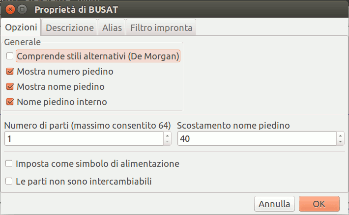
It is important to set the number of units and check all units are interchangeable and has alternate body style, as applicable, because these settings affect how pins and graphics are added to each symbol unit.
If you change the number of units per package after adding the pins to the symbol, you will need to do extra work to add pins and graphics for the additional units. The pins and graphics would have been automatically added to each unit had these properties been correctly set initially. Nevertheless, it is possible to modify these properties at any time.
The graphic options Show pin number and Show pin name define the visibility of the pin number and pin name text. The option Place pin names inside defines the pin name position relative to the pin body. The pin names will be displayed inside the symbol outline if the option is checked. In this case the Pin Name Position Offset property defines the shift of the text away from the body end of the pin. A value from 0.02 to 0.05 inches is usually reasonable.
The example below shows a symbol with the Place pin name inside option unchecked. Notice the position of the names and pin numbers.
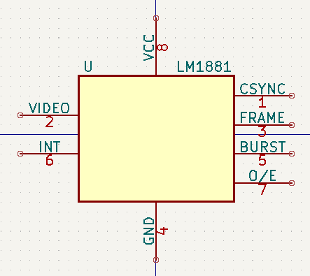
Symbol Name, Description, and Keywords
Symbol name is the symbol’s name in the library. Symbols are identified by a combination of the library and symbol name.
In previous versions of KiCad, the symbol name was linked to the Value field. This link is removed in KiCad 7.0 and later.
The symbol description should contain a brief description of the component, such as the component function, distinguishing features, and package options. The keywords should contain additional terms related to the component. Keywords are used primarily to assist in searching for the symbol.
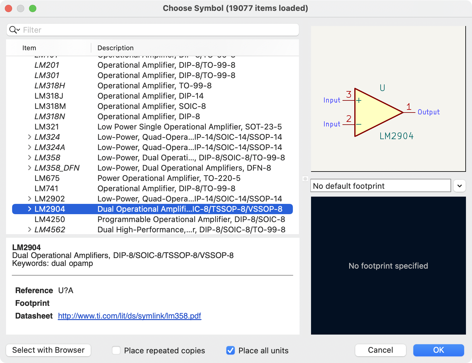
A symbol’s name, description, and keywords are all used when searching for symbols in the Symbol Editor and Add a Symbol dialog. The description and keywords are displayed in the Symbol Library Browser and Add a Symbol dialog.
Footprint Filters
The footprint filters tab is used to define which footprints are appropriate to use with the symbol. The filters can be applied in the Footprint Assignment tool so that only appropriate footprints are displayed for each symbol.
Multiple footprint filters can be defined. Footprints that match any of the filters will be displayed; if no filters are defined, then all footprints will be displayed.
Filters can use wildcards: * matches any number of characters, including zero, and ? matches zero or one characters. For example, SOIC-* would match the SOIC-8_3.9x4.9mm_P1.27mm footprint as well as any other footprint beginning with SOIC-. The filter SOT?23 matches SOT23 as well as SOT-23.
Definizione piedini per simboli multipli e rappresentazioni simboliche alternative
Se il simbolo possiede uno stile corpo alternativo definito, sarà necessario selezionarne uno alla volta per la modifica. Per modificare la rappresentazione normale, fare clic su ![]() .
.
To edit the alternate representation, click on the ![]() icon. Use the
icon. Use the  unit selection dropdown to select the unit you wish to edit.
Elementi grafici
Gli elementi grafici formano la rappresentazione di un simbolo e non contengono informazioni di connessioni elettriche. Vengono creati usando i seguenti strumenti:
-
Linee e poligoni definiti da punti di inizio e fine.
-
Rettangoli definiti da due angoli diagonali.
-
Cerchi definiti da centro e raggio.
-
Archi definiti da punti di inizio e fine dell’arco ed il suo centro. Un arco va da 0° a 180°.
La barra strumenti verticale sul lato destro della finestra principale permette di piazzare tutti gli elementi grafici richiesti per progettare la rappresentazione di un simbolo.
Appartenenza di elementi grafici
Ogni elemento grafico (linea, arco, cerchio, ecc.) può essere definito come comune a tutte le unità e/o stili di corpi o specifico di una data unità e/o stile corpo. Le opzioni dell’elemento sono accessibili facilmente facendo clic destro sull’elemento per mostrare il menu contestuale per l’elemento selezionato. Di seguito è mostrato il menu contestuale per un elemento linea.
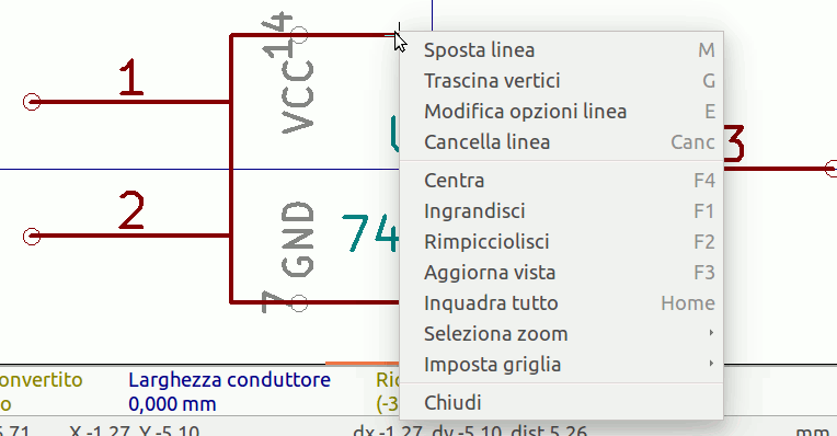
Si può anche fare doppio clic sinistro su un elemento per modificare le sue proprietà. Di seguito viene mostrata la finestra di dialogo delle proprietà di un elemento poligono.
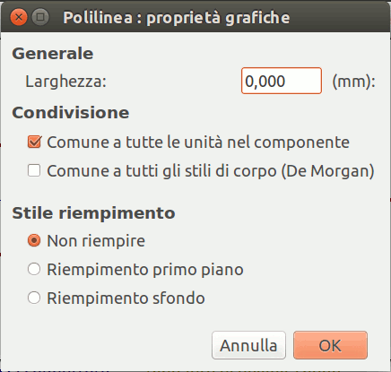
Le proprietà di un elemento grafico sono:
-
Border determines whether the the shape’s outline should be drawn.
-
Width and color define the line width and color of the border. A border width of
0uses the schematic’s default symbol line width. Style determines the line style of the border (solid, dashed, dotted, etc.). -
Fill Style determines if the shape defined by the graphical element is to be drawn unfilled or filled. The fill color can be the color theme’s body outline color, body background color, or a custom color.
-
Common to all units in symbol determines if the graphical element is drawn for each unit in symbol with more than one unit per package or if the graphical element is only drawn for the current unit.
-
Common to all body styles (De Morgan) determines if the graphical element is drawn for each symbolic representation in symbols with an alternate body style or if the graphical element is only drawn for the current body style.
-
Private to Symbol Editor causes the shape to be visible only when the symbol is edited in the Symbol Editor. The shape will be hidden when the symbol is added to a schematic.
Elementi di testo grafico
![]() permette la creazione di testo grafico. Il testo grafico viene automaticamente orientato per essere leggibile, anche se il simbolo viene reso speculare. Si noti che gli elementi di testo grafico non sono campi del simbolo.
permette la creazione di testo grafico. Il testo grafico viene automaticamente orientato per essere leggibile, anche se il simbolo viene reso speculare. Si noti che gli elementi di testo grafico non sono campi del simbolo.
Unità multiple per simbolo e stili di corpo alternativi
I simboli possono avere fino a due rappresentazioni simboliche (una standard e una alternativa, spesso chiamata "equivalente DeMorgan") e/o avere più di una unità per contenitore (per esempio le porte logiche). Alcuni simboli possono avere più di una unità per ogni contenitore con simboli e configurazioni di piedinatura differenti.
For example, consider a relay with two switches, which can be designed as a symbol with three different units: a coil, switch 1, and switch 2. Designing a symbol with multiple units per package and/or alternate body styles is very flexible. A pin or a body symbol item can be common to all units or specific to a given unit or they can be common to both symbolic representation so are specific to a given symbol representation.
By default, pins are specific to a unit and body style. When a pin is common to all units or all body styles, it only needs to be created once. This is also the case for the body style graphic shapes and text, which may be common to each unit, but typically are specific to each body style.
To add additional units to a symbol, set the Number of Units property to the appropriate number in the Symbol Properties dialog. By default, symbol units are named Unit A, Unit B, etc., but you can set an arbitrary name for the current unit using Edit → Set Unit Display Name….
To add an alternate body style, set the Has alternate body style (De Morgan) property in the Symbol Properties dialog.
Esempio di simbolo multiunità non interscambiabili
Come esempio di simbolo con più unità non intercambiabili, si consideri un relè con 3 unità per contenitore: una bobina, l’interruttore 1 e l’interruttore 2.
The three units are not all the same, so All units are interchangeable should be deselected in the Symbol Properties dialog. Alternatively, this option could have been specified when the symbol was initially created.
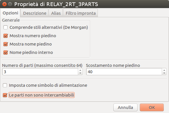
Unit A
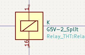
Unit B
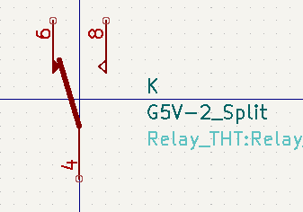
Unit C
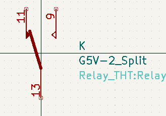
L’unità A non ha lo stesso simbolo e disposizione di pin delle unità B e C, perciò le unità non sono intercambiabili.
|
Synchronized Pins Edit Mode can be enabled by clicking the
|
Creazione e modifica di piedini
You can create and insert a pin by clicking on the ![]() button. Pin properties can be edited by double clicking on the pin. You can also delete or move pins that you have already added. Pins must be created carefully, because any error will have consequences on the PCB design.
button. Pin properties can be edited by double clicking on the pin. You can also delete or move pins that you have already added. Pins must be created carefully, because any error will have consequences on the PCB design.
Panoramica piedino
A pin is defined by its graphical representation, its name, and its number. The pin’s name and number can contain letters, numbers, and symbols, but not spaces. For the Electrical Rules Check (ERC) tool to be useful, the pin’s electrical type (input, output, tri-state…) must also be defined correctly. If this type is not defined properly, the schematic ERC check results may be invalid.
Note importanti:
-
Symbol pins are matched to footprint pads by number. The pin number in the symbol must match the corresponding pad number in the footprint.
-
Do not use spaces in pin names and numbers. Spaces will be automatically replaced with underscores (
_). -
To define a pin name with an inverted signal (overbar) use the
~(tilde) character followed by the text to invert in braces. For example~{FO}Owould display FO O. -
Se il nome pin è vuoto, il pin viene considerato senza nome.
-
I nomi di pin possono essere ripetuti in un simbolo.
-
I numeri di pin devono essere univoci in un simbolo.
Proprietà piedino
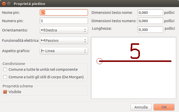
La finestra di dialogo delle proprietà del pin permette di modificare tutte le caratteristiche di un pin. Questa finestra di dialogo salta fuori automaticamente quando si crea un pin o facendo doppio clic su un pin già esistente. Questa finestra di dialogo permette di modificare:
-
Nome e dimensione testo del pin.
-
Numero e dimensione testo del pin.
-
Lunghezza pin.
-
Tipo elettrico e stile grafico del piedino.
-
Unità e appartenenza a rappresentazioni alternative.
-
Visibilità pin.
Stili grafici pin
The different pin graphic styles are shown in the figure below. These styles are purely graphical and do not affect the pin’s electrical type.
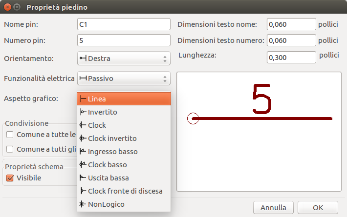
Tipi elettrici del pin
Each pin in a symbol has an electrical type, such as input, output, or tri-state.
Choosing the correct electrical type is important for the schematic ERC tool. ERC will check that pins are connected appropriately, for example ensuring that input pins are driven and power inputs receive power from an appropriate source.
You can use the Pin Conflicts Map in the schematic editor to configure which pin types are allowed to connect and which will conflict. The default Pin Conflicts settings are briefly explained below. For more information, see the ERC documentation.
Additionally, some pin types have special behavior outside of ERC: in the router, pads corresponding to a free pin can be connected to copper of any other net without causing a DRC error, and pads corresponding to stacked unconnected pins do not need to be connected to each other.
Pin Type |
Description |
Input |
A pin which is exclusively an input. The default Pin Conflicts settings allow input pins to connect to most other types of pin. |
Output |
A pin which is exclusively an output. The default Pin Conflicts settings allow output pins to connect to most types of pin that aren’t also outputs. |
Bidirectional |
A pin that can be either an input or an output, such as a microcontroller data bus pin. The default Pin Conflicts settings allow bidirectional pins to connect to most other types of pins, though there are a few more restrictions than with input pins. |
Tri-state |
A three state output pin (high, low, or high impedance). The default Pin Conflicts settings allow tri-state pins to connect to most other types of pins, but warnings are generated when they are connected to most types of output or power pins. |
Passive |
A pin that is not connected to active electronics, for example pins on a resistor or connector. The default Pin Conflicts settings allow passive pins to connect to most other types of pin. |
Free |
A pin that does not electrically affect the operation of the device. These pins typically represent package leads that are not internally connected to the chip. The default Pin Conflicts settings allow free pins to connect to most other types of pin. In the PCB editor, pads corresponding to free pins can be connected to copper of any other net without causing a DRC error. |
Unspecified |
A pin which has an unspecified type. With the default Pin Conflicts settings, ERC generates warnings when unspecified pins are connected to most other types of pins. |
Power input |
A pin that powers the device. The default Pin Conflicts settings allow power input pins to connect to most other pin types. However, power input pins that are not connected to a power output pin generate an ERC violation. Additionally, power input pins that are marked invisible are automatically connected to the net with the same name as the pin. See the Power Symbols section for more information. |
Power output |
A pin that provides power to other pins, such as a regulator output. The default Pin Conflicts settings allow power output pins to connect to most types of output pins, but not input pins. |
Open collector |
An open collector logic output. The default Pin Conflicts settings allow open collector pins to connect to most input pins and other open collector pins, but not to most other types of outputs. |
Open emitter |
An open emitter logic output. The default Pin Conflicts settings allow open collector pins to connect to most input pins and other open emitter pins, but not to most other types of outputs. |
Unconnected |
A pin that should not be connected to anything. The default Pin Conflict settings do not allow pins of type unconnected to connect to any other type of pin, and ERC will not generate an "unconnected pin" violation when pins of this type are left unconnected. If a footprint has multiple pads corresponding to a single unconnected pin, the pads do not need to be connected to each other in the board. When multiple pins of type unconnected are stacked in a symbol, they are connected to separate nets, whereas stacked pins of other types are connected to the same net. Note that this pin type is different than placing a no connect flag on a pin in the schematic. The unconnected pin type indicates that the pin should never be connected in any schematic, while a no connect flag indicates that the pin is intentionally unconnected in the current schematic. |
Pushing Pin Properties to Other Pins
You can apply the length, name size, or number size of a pin to the other pins in the symbol by right clicking the pin and selecting Push Pin Length, Push Pin Name Size, or Push Pin Number Size, respectively. All other pins in the symbol will be updated.
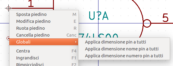
Definizione piedini per componenti multipli e rappresentazioni simboliche alternative
I simboli con più unità e/o rappresentazioni grafiche sono particolarmente problematici durante la creazione e la modifica dei pin. La maggior parte dei pin è specifica per ciascuna unità di simbolo (perché ogni unità ha un diverso set di pin) e per ogni stile del corpo (perché la forma e la posizione sono diverse tra lo stile del corpo normale e la forma alternativa).
L’editor della libreria dei simboli consente la creazione simultanea di pin. Per impostazione predefinita, le modifiche apportate a un pin vengono apportate per tutte le unità di un simbolo a più unità e ad entrambe le rappresentazioni per i simboli con una rappresentazione simbolica alternativa. L’unica eccezione è il tipo grafico e il nome del pin, che rimangono scollegati tra le unità dei simboli e gli stili del corpo. Questa dipendenza è stata stabilita per consentire una più facile creazione e modifica dei pin nella maggioranza dei casi. Questa dipendenza può essere disabilitata attivando l’icona ![]() sulla barra degli strumenti principale. Ciò consentirà di creare pin per ogni unità e rappresentazione in modo completamente indipendente.
sulla barra degli strumenti principale. Ciò consentirà di creare pin per ogni unità e rappresentazione in modo completamente indipendente.
I pin possono essere comuni o specifici per diverse unità. I pin possono anche essere comuni a entrambe le rappresentazioni simboliche o specifici di ciascuna rappresentazione simbolica. Quando un pin è comune a tutte le unità, deve essere disegnato solo una volta. I pin sono impostati come comuni o specifici nella finestra di dialogo delle proprietà dei pin.
An example is the output pin in the 7400 quad dual input NAND gate. Since there are four units and two symbolic representations, there are eight separate output pins defined in the symbol definition. When creating a new 7400 symbol, unit A of the normal symbolic representation will be shown in the library editor. To edit the pin style in the alternate symbolic representation, it must first be enabled by clicking the ![]() button on the tool bar. To edit the pin number for each unit, select the appropriate unit using the drop down control.
button on the tool bar. To edit the pin number for each unit, select the appropriate unit using the drop down control.
Tabella pin
Un altro modo per modificare i pin è usando la tabella pin, che è accessibile tramite l’icona ![]() . La tabella pin mostra tutti i pin nel simbolo e le relative proprietà in una vista tabellare, quindi è utile per apportare modifiche in blocco ai pin.
. La tabella pin mostra tutti i pin nel simbolo e le relative proprietà in una vista tabellare, quindi è utile per apportare modifiche in blocco ai pin.
Qualsiasi proprietà del pin può essere modificata facendo clic sulla cella appropriata. I pin possono essere aggiunti e rimossi rispettivamente con le icone ![]() e
e ![]() .
.
You can edit the same property for multiple pins simultaneously by grouping pins. Pins can be automatically grouped by name, or you manually group several pins by selecting them and clicking Group Selected. Click the ![]() button to clear the manual grouping. You can also filter the table to only display pins in certain units.
button to clear the manual grouping. You can also filter the table to only display pins in certain units.
| Le colonne della tabella pin possono essere visualizzate o nascoste facendo clic con il pulsante destro del mouse sulla riga dell’intestazione e selezionando o deselezionando le colonne aggiuntive. Alcune colonne sono nascoste per impostazione predefinita. |
Lo screenshot qui sotto mostra la tabella pin per un operazionale quadruplo.
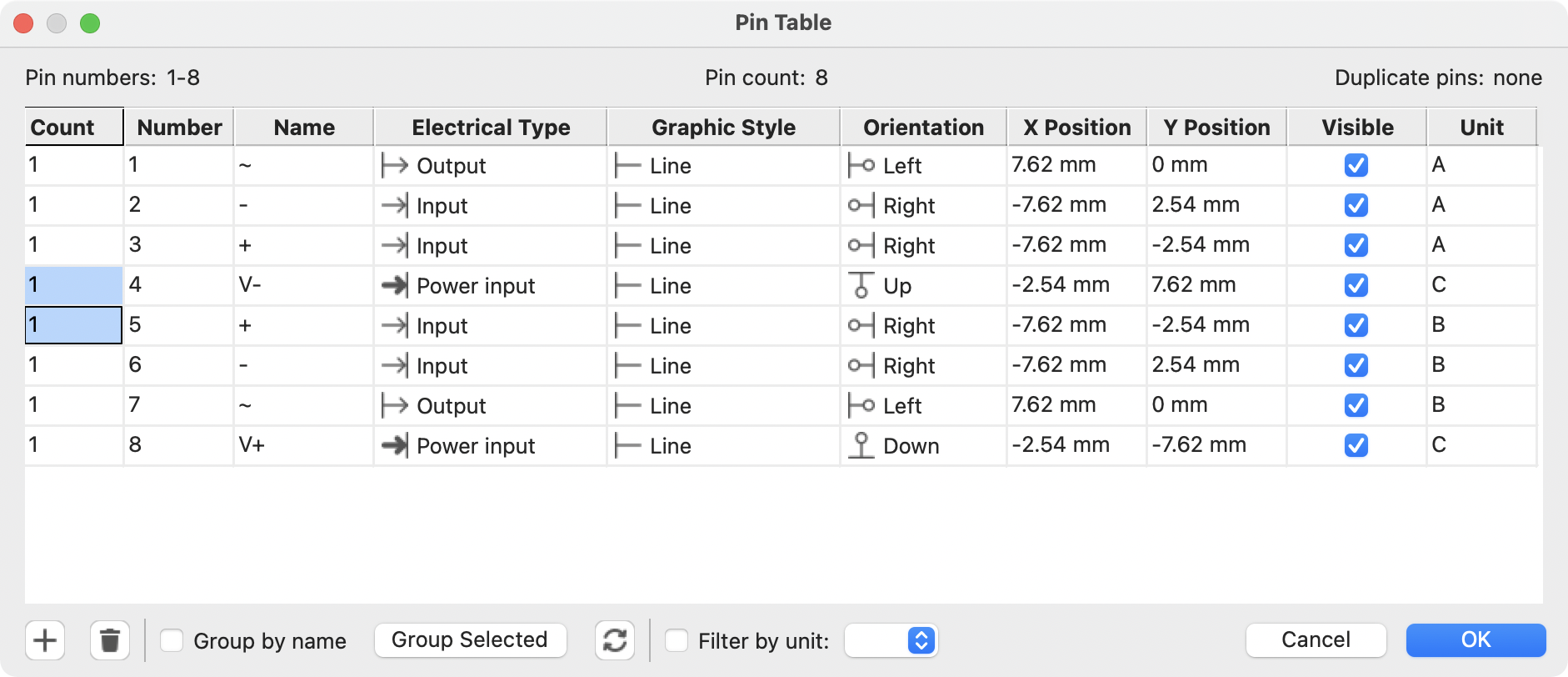
Definizioni alternative dei pin
Ai pin possono essere aggiunte definizioni alternative. Le definizioni di pin alternative consentono ad un utente di selezionare un nome, un tipo elettrico e uno stile grafico diversi per pin, quando il simbolo viene posizionato sullo schema. Tutto ciò può essere utile per i pin che hanno più funzioni, come i pin di un microcontrollore.
Le definizioni di pin alternative vengono aggiunte con finestra di dialogo Proprietà pin come mostrato di seguito. Ogni definizione alternativa contiene un nome pin, un tipo elettrico e uno stile grafico. Questo pin di microcontrollore ha tutte le sue funzioni periferiche definite nel simbolo come nomi di pin alternativi.
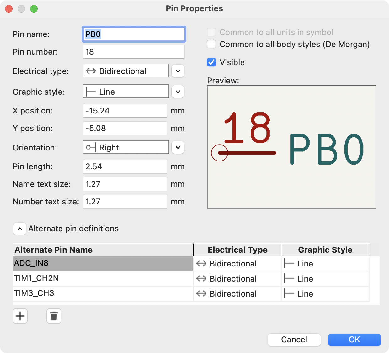
Le definizioni di pin alternative vengono selezionate nell’editor degli schemi una volta che il simbolo sia stato inserito nello schema. Il pin alternativo viene assegnato nella scheda Assegnazioni pin alternativi della finestra di dialogo Proprietà simbolo. Le definizioni alternative sono selezionabili nell’elenco a discesa nella colonna Assegnazione alternativa.
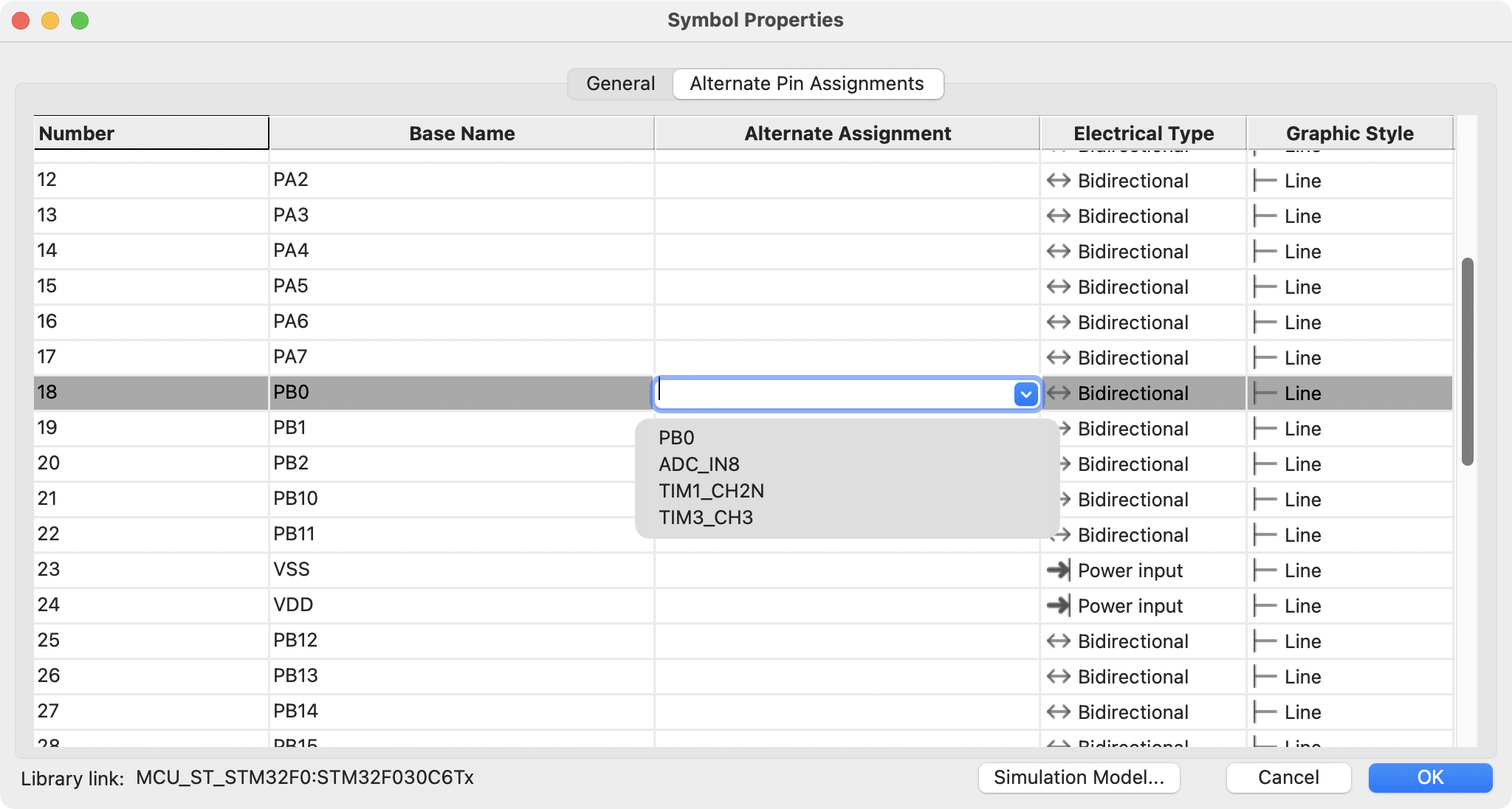
Campi del simbolo
All library symbols are defined with four default fields. The reference designator, value, footprint assignment, and datasheet link fields are created whenever a symbol is created or copied. Only the reference designator is required.
The Footprint field, if used, contains a reference to a footprint for the symbol. The format is LIBNAME:FOOTPRINTNAME, where LIBNAME is the name of the footprint library in the footprint library table (see the Footprint Library Table section in the PCB Editor manual) and FOOTPRINTNAME is the name of the footprint in the library LIBNAME.
I simboli definiti nelle librerie sono in genere definiti solo con questi quattro campi predefiniti. Campi aggiuntivi come fornitore, numero di parte, costo unitario, ecc. possono essere aggiunti ai simboli della libreria, ma generalmente questo viene fatto nell’editor dello schema in modo che i campi aggiuntivi possano essere applicati a tutti i simboli nello schema.
| A convenient way to create additional empty symbol fields is to use define field name templates. Field name templates define empty fields that are added to each symbol when it is inserted into the schematic. Field name templates can be defined globally (for all schematics) in the Schematic Editor Preferences, or they can be defined locally (specific to each project) in the Schematic Setup dialog. |
| If you want to manage a large amount of component data in symbol fields, consider using database libraries. |
Modifica campi del simbolo
To edit an existing symbol field, double-click the field, select it or hover and press E, or right-click on the field text and select Properties….
Per aggiungere nuovi campi, eliminare campi facoltativi o modificare campi esistenti, utilizzare l’icona ![]() sulla barra degli strumenti principale per aprire la finestra di dialogo Proprietà simbolo.
sulla barra degli strumenti principale per aprire la finestra di dialogo Proprietà simbolo.
Fields are text information associated with the symbol. Do not confuse them with text in the graphic representation of a symbol.
Creating Power Symbols
Power symbols are symbols that are used to label a wire as part of a global power net, like VCC or GND. The behavior of power symbols is described in the electrical connections section. Power symbols are handled and created the same way as normal symbols, but there are several additional considerations described below.
It may be useful to place power symbols in a dedicated library. KiCad’s symbol library places power symbols in the power library, and users may create libraries to store their own power symbols. If the Define as power symbol box is checked in a symbol’s properties, that symbol will appear in the Schematic Editor’s Add Power Symbol dialog for convenient access.
Di seguito è riportato un esempio di simbolo di potenza GND.
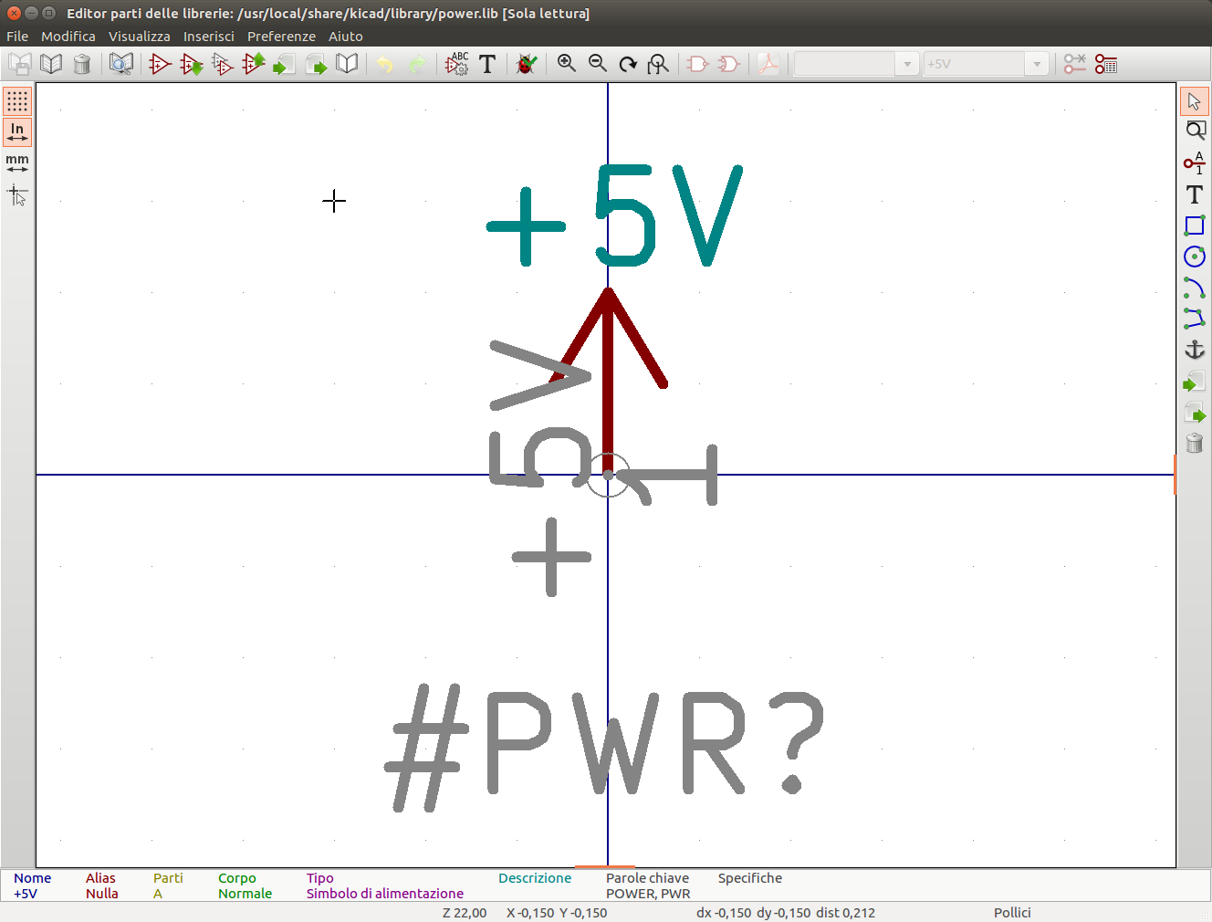
Power symbols consist of a pin of type "Power input" that is marked invisible. They must also have the Define as power symbol property checked. Invisible power input pins have a special property of making implicit global connections based on the pin name.
| If the power symbol has the Define as power symbol property checked, the power input pin does not need to be marked invisible. However, the convention is to make these pins invisible anyway. |
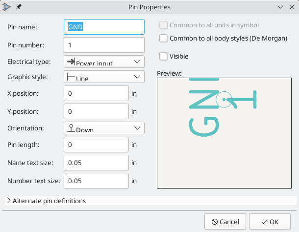
Per creare un simbolo di potenza, seguire questi passi:
-
Add a pin of type Power input, with Visible unchecked, and the pin named according to the desired net. Make the pin number
1, the length0, and set the graphic style to Line. The pin name establishes the connection to the net; in this case the pin will automatically connect to the netGND. The pin number, length, and line style do not matter electrically. -
Posiziona il pin sull’ancora del simbolo.
-
Usa gli strumenti forma per disegnare la grafica del simbolo.
-
Set the symbol value. The symbol value does not matter electrically, but it is displayed in the schematic. To eliminate confusion, it should match the pin name (which determines the connected net name).
-
Check the Define as power symbol box in Symbol Properties window. This makes the symbol appear in the Add Power Symbol dialog, makes the
Valuefield read-only in the schematic, prevents the symbol from being assigned a footprint, and excludes the symbol from the board, BOM, and netlists. -
Set the symbol reference and uncheck the Show box. The reference text is not important except for the first character, which should be
#. For the power symbol shown above, the reference could be#GND. Symbols with references that begin with#are not added to the PCB, are not included in Bill of Materials exports or netlists, and they cannot be assigned a footprint in the footprint assignment tool. If a power symbol’s reference does not begin with#, the character will be inserted automatically when the annotation or footprint assignment tools are run.
An easier method to create a new power symbol is to use another symbol as a starting point, as described earlier.
| The connected net name is determined by the power symbol’s pin name, not the name or value of the symbol. When modifying an existing power symbol, make sure to rename the pin so that the new symbol connects to the appropriate power net. This means that power symbol net names can only be changed in the symbol editor, not in the schematic. |
Checking Symbols
The Symbol Editor can check for common issues in your symbols. Run the symbol checker using the ![]() button in the top toolbar.
button in the top toolbar.
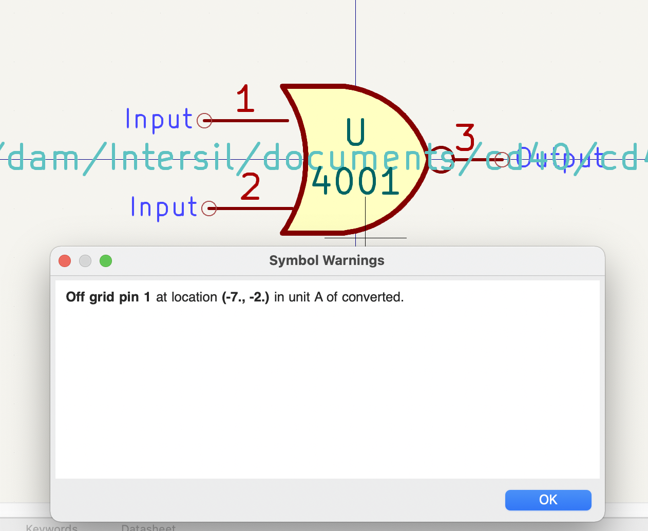
The symbol checker checks for:
-
Pins that are off-grid
-
Pins that are duplicated between symbol units
-
Incorrectly designed power symbols. Power symbols should have:
-
A single unit
-
No alternate body styles
-
A single pin which is either of type Power Output (see PWR_FLAG) or invisible and of type Power Input (see power symbols)
-
-
Illegal reference designator prefixes: reference designator prefixes should not end with a number or
? -
Hidden Power Input pins in non-power symbols: these create implicit connections and are not recommended
Browsing symbol libraries
The Symbol Library Browser allows you to quickly examine the contents of symbol libraries. The Symbol Library Viewer can be accessed by clicking ![]() icon on the main toolbar, View → Symbol Library Browser, or clicking Select With Browser in the Choose Symbol window.
icon on the main toolbar, View → Symbol Library Browser, or clicking Select With Browser in the Choose Symbol window.
To examine the contents of a library, select a library from the list on the left hand pane. All symbols in the selected library will appear in the second pane. Select a symbol name to view the symbol.
Facendo doppio clic sul nome di un simbolo o utilizzando il pulsante ![]() si aggiunge il simbolo allo schema.
si aggiunge il simbolo allo schema.
La barra superiore contiene i seguenti comandi:
|
Open the selected symbol in the Choose Symbol window. |
|
Select previous symbol in library. |
|
Select next symbol in library. |
|
Zoom tools. |
|
Select standard or alternate De Morgan representation of symbol, if applicable. |
|
Select the unit of a multi-unit symbol. |
|
Open the symbol’s datasheet, if it is defined. |
|
Insert current symbol into the schematic. |
Simulatore
KiCad provides an embedded electrical circuit simulator using ngspice as the simulation engine. All but the simplest simulations will require you to add simulation models to your symbols before you can simulate your schematic.
When working with the simulator, the official Simulation_SPICE symbol library may be useful. It contains common symbols used for simulation, like voltage/current sources and transistors with pins numbered to match the ngspice node order specification.
KiCad includes a few demo projects to illustrate the simulator’s capabilities. They can be found in the demos/simulation directory.
Value notation
The simulator supports several notations for writing numerical values:
-
Plain notation :
10100,0.003, -
Scientific notation:
1.01e4,3e-3, -
Prefix notation:
10.1k,3m. -
RKM notation:
4k7,10R.
You can mix prefix and scientific notations. As such, 3e-4k is a valid input and is equivalent to 0.3. The list of valid prefixes is shown below. The prefixes are case sensitive.
| Prefix | Meaning | Value |
|---|---|---|
a |
atto |
10-18 |
f |
femto |
10-15 |
p |
pico |
10-12 |
n |
nano |
10-9 |
u |
micro |
10-6 |
m |
milli |
10-3 |
k |
kilo |
103 |
M |
mega |
106 |
G |
giga |
109 |
T |
tera |
1012 |
P |
peta |
1015 |
E |
exa |
1015 |
Raw SPICE Element models and directives are passed to ngspice directly, without KiCad reformatting the values for ngspice to consume. Ngspice uses a different, case-insensitive notation: 1 mega (106) is denoted there as 1Meg, while 1M is 1 milli (10-3). Depending on the compatibility mode selected, ngspice may not support the same value notations as KiCad, so care should be taken when using raw SPICE elements and simulation directives.
|
Assegnazione modelli
You need to assign simulation models to symbols before you can simulate your circuit.
Each symbol can have only one model assigned, even if the symbol consists of multiple units. For symbols with multiple units, you should assign the model to the first unit.
SPICE model information is stored as text in symbol fields. Therefore you may define it in either the symbol editor or the schematic editor. To assign a simulation model to a symbol, open the Symbol Properties dialog and click the Simulation Model… button, which opens the Simulation Model Editor dialog.
You can exclude a symbol from simulation entirely by checking the exclude from simulation checkbox in the Symbol Properties dialog.
Inferred models
Resistor, inductor, and capacitor models can be inferred, which means that KiCad will detect that they are passives and automatically assign an appropriate simulation model. Therefore they do not require any special settings; users only need to set the Value field of the symbol.
KiCad infers simulation models for symbols based on the following criteria:
-
The symbol has exactly two pins,
-
The reference designator begins with
R,LorC.
Inferred models are ideal models. If the simulation requires a non-ideal model, you must explicitly assign a model.
Built-in models
KiCad offers several standard simulation models. They do not require an external model file. The following devices are available:
-
Resistors (including potentiometers), capacitors, inductors
-
Transmission lines
-
Switches
-
Voltage and current sources
-
Diodes
-
Transistors (BJT, MOSFET, MESFET, and JFET)
-
Raw SPICE elements
To add a built-in model to a symbol, open the Simulation Model Editor dialog (Symbol Properties → Simulation Model…) and select Built-in SPICE model.
Refer to the ngspice documentation for more details about these models.
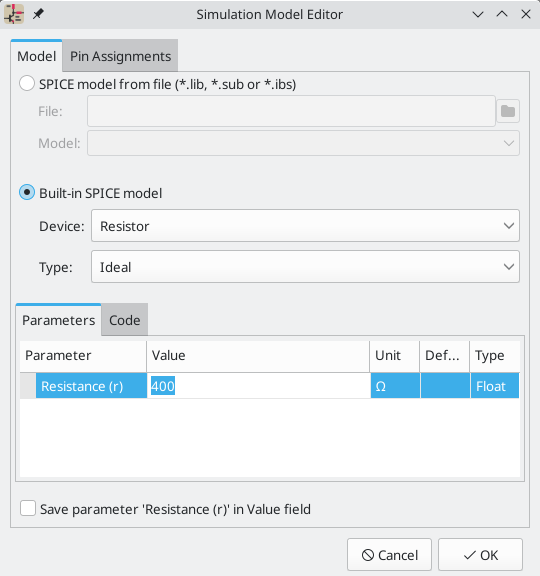
Device sets the type of device to simulate: a resistor, BJT, voltage source,
etc. This value is stored in the symbol’s Sim.Device field.
Type selects the type of model to use for the device. Most devices have
several types of models to choose from, which may vary in their degree of
accuracy, which characteristics they are optimized for, and what parameters they
have available. Refer to the ngspice documentation for details. This value is
stored in the symbol’s Sim.Type field.
The parameters tab displays the parameters of the model and lets you edit them. For example, a resistor’s resistance, a voltage source’s waveform, a MOSFET’s width and length, etc. Any parameters that differ from the model’s defaults are stored in the symbol’s Sim.Params field.
The code tab displays the generated SPICE model as it will be written to the SPICE netlist for simulation.
The Save parameter '<parameter name>' in Value field checkbox uses the symbol’s Value field for storing parameters instead of the Sim.Params field. This may make it easier to edit simple models from the schematic, without opening the Simulation Model Editor. This option is only available for ideal passive models (R, L, C) and DC sources. If the field Sim.Params exists in the symbol, it will take priority over the Value field.
Library models
KiCad can load SPICE models from external files. The models must be in a standard SPICE format and not encrypted.
To load a model from an external file, open the Simulation Model Editor dialog (Symbol Properties → Simulation Model…) and select SPICE model from file.
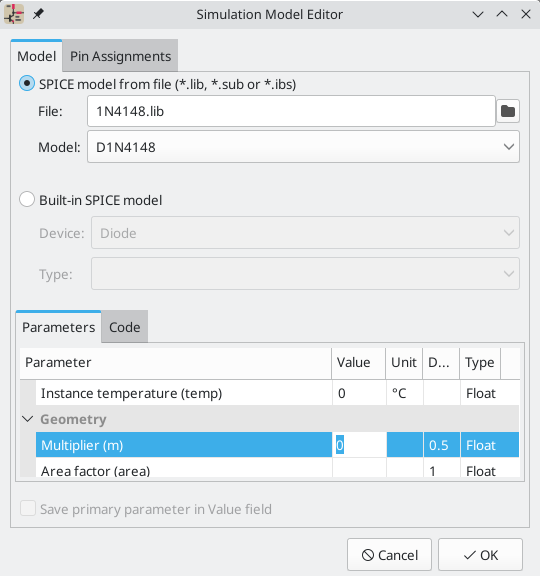
File is the path to the model file to use. The path can be absolute or
relative to the project folder. The path can also be relative to the value of
SPICE_LIB_DIR if you have
defined that path variable.
The library filename is saved in the symbol’s Sim.Library field.
Model is the name of the desired model in the model file. If the file
contains multiple models, they will all be listed in the dropdown. The selected
model is listed in the symbol’s Sim.Name field.
Parameters can be overridden (or additional parameters specified) using the parameters tab. All parameters specified in the selected model or the parameters tab are stored in the symbol’s Sim.Params field.
The code tab displays the generated SPICE model as it will be written to the SPICE netlist for simulation.
| KiCad does not ship with SPICE models for symbols. SPICE models are usually available from device manufacturers. |
Library models (IBIS)
IBIS (I/O Buffer Information Specification) files are an alternative to SPICE models for modeling the behavior of input/output buffers on digital parts. In order to load an IBIS file, users should follow the procedure for SPICE library models, but provide a .ibs file.
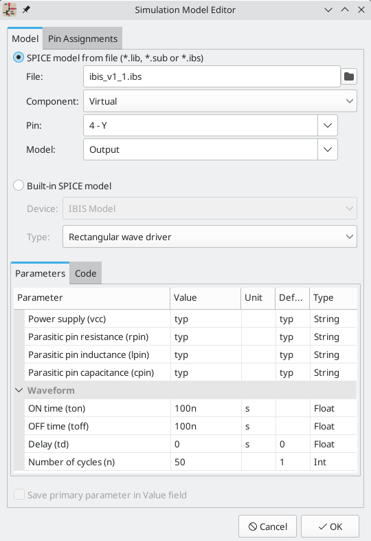
File is the path to the model file to use. The path can be absolute or
relative to the project folder. The path can also be relative to the value of
SPICE_LIB_DIR if you have
defined that path variable.
The library filename is saved in the symbol’s Sim.Library field. If an IBIS
model file is loaded, the remaining fields in the dialog will relate to the IBIS
model.
Component selects which component from the IBIS file to use, as IBIS files
can contain multiple components. The component name is saved in the symbol’s
Sim.Name field.
Pin selects which pin in the IBIS model to simulate. The selected pin must
be mapped to a symbol pin in the Pin Assignments tab. The chosen pin’s
number is saved in the symbol’s Sim.Ibis.Pin field.
Model is the list of models available for the selected pin, for example an
input or an output. The chosen model name is saved in the symbol’s
Sim.Ibis.Model field.
Type selects what the pin should do in the simulation. A pin can be a passive
device that doesn’t drive any value; it can be a DC driver that drives
high, low, or high-impedance; or it can be a rectangular wave or
PRBS driver. This value is stored in the symbol’s Sim.Type field.
The Parameters tab lets you see and edit the parameters of the model. For each parameter, you can switch between a minimum, typical, or maximum value, as defined in the IBIS file. You can also choose the parameters of the driven waveform, depending on the pin’s chosen type. Any parameters that differ from the defaults are stored in the symbol’s Sim.Params field.
| KiCad does not ship with IBIS models for symbols. IBIS models are usually available from device manufacturers. |
KiCad’s Simulation_SPICE symbol library provides several symbols that may be useful for IBIS simulations. IBIS_DEVICE can be used for device (input) pins, while IBIS_DRIVER can be used for simulating driver pins. There are also variants of each for differential pins.
|
Pin Assignment
Simulation models may have their pins numbered differently than the corresponding symbol. For example, SPICE models for diodes usually consider pin 1 to be the anode, while schematic symbols are usually drawn with pin 1 as the cathode.
You can use the Simulation Model Editor’s Pin Assignments tab to map the symbol’s pins to the simulation model pins.
| Always make sure symbol pins are correctly mapped to simulation model pins. |
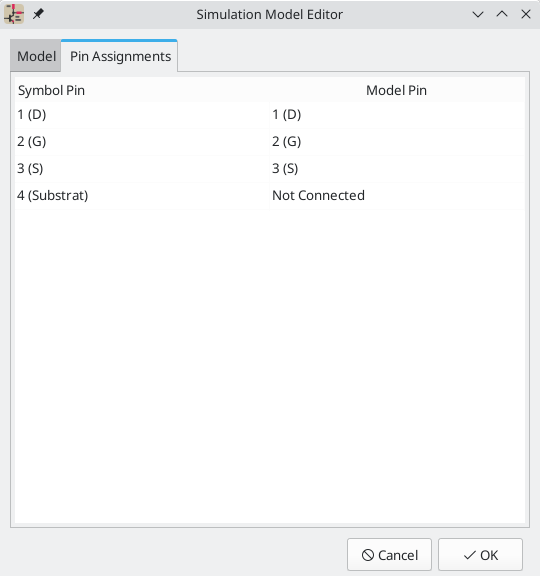
The left column displays the name and number of each symbol pin. For each symbol pin, you can select the corresponding pin from the simulation model in the dropdown in the right column.
When you use a subcircuit model, the dialog displays the model’s code under the pin assignments for use as a reference while assigning pins.
SPICE directives
It is possible to add SPICE directives by placing them in text fields on a schematic sheet. This approach is convenient for defining the default simulation type. The list of supported directives in text fields is:
-
Directives starting with a dot (e.g.
.tran 10n 1m) -
Coupling coefficients for inductors (e.g.
K1 L1 L2 0.89)
It is not possible to place additional components using text fields.
If a simulation command is included in schematic text, the simulator will use it as the simulation command when you open the simulator. However, you can override it in the Simulation Command dialog.
Refer to the ngspice documentation for more details about SPICE directives.
Running simulations
User Interface
To run a simulation, open the SPICE simulator dialog by clicking Inspect → Simulator in the schematics editor window or using the ![]() button in the top toolbar.
button in the top toolbar.
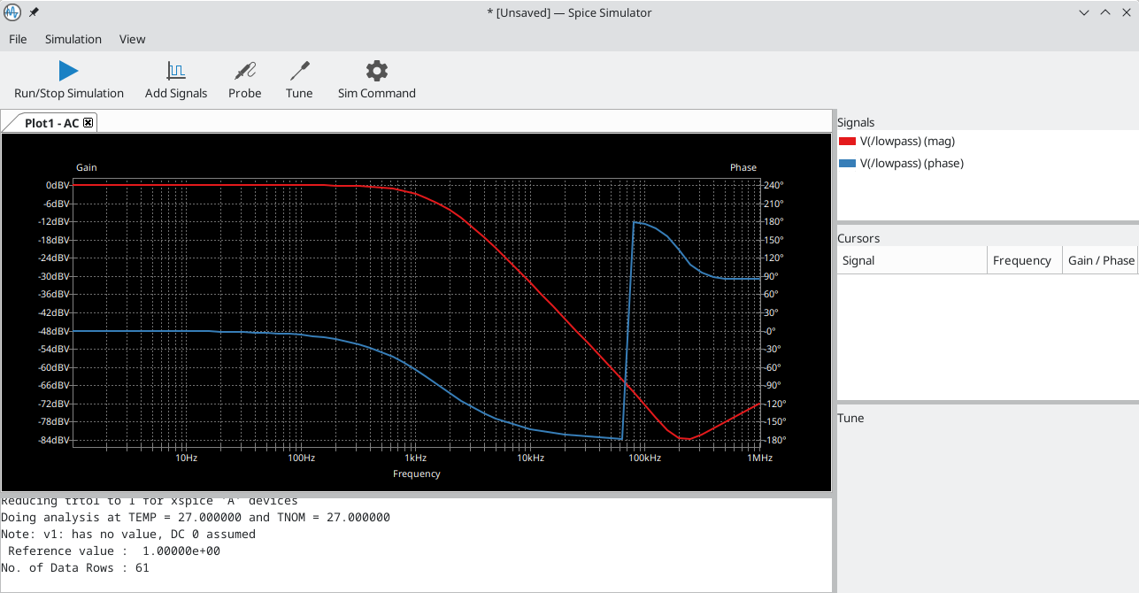
La finesta è divisa in diverse sezioni:
-
The top of the window has a toolbar with buttons for commonly used actions.
-
The main part of the window graphically shows the simulation results. Signals need to be probed before they are displayed in the plot.
-
Below the plot panel, the output console shows logs from the ngspice simulation engine.
-
The right side of the window displays a list of plotted signals, a list of active cursors, and a tuning tool for adjusting component values based on simulation results.
Workbooks
Workbooks are files that store information about the simulation environment, including simulation setup parameters and the list of displayed signals. They can be used to store the setup for a set of analyses, which can then be reloaded and rerun at a later time.
You can save and load a workbook using File → Save Workbook and File → Open Workbook.
| Workbooks store simulation setup information, but they do not store simulation results. You can export simulation results to PNG (graphics) or CSV (data points) with File → Export Current Plot as PNG… and File → Export Current Plot as CSV…. |
Running a Simulation
Before running a simulation, you need to select a simulation type and choose the simulation parameters. This can be done using Simulation → Settings… or the Sim Command button (![]() ) and then selecting one of the available analysis types:
) and then selecting one of the available analysis types:
-
AC
-
DC Transfer
-
Operating Point
-
Transient
-
Custom
Analysis types are further explained in the ngspice documentation.
An alternative way to configure a simulation is to type SPICE directives into text fields on schematics. Any text field directives related to a simulation command are overridden by the settings selected in the dialog. This means that once a simulation has run, the dialog overrides the schematic directives until the simulator is reopened.
Once the simulation command is set, users can start a simulation with Simulation → Start Simulation (Ctrl+R) or the Run/Stop Simulation button (![]() ).
).
AC analysis
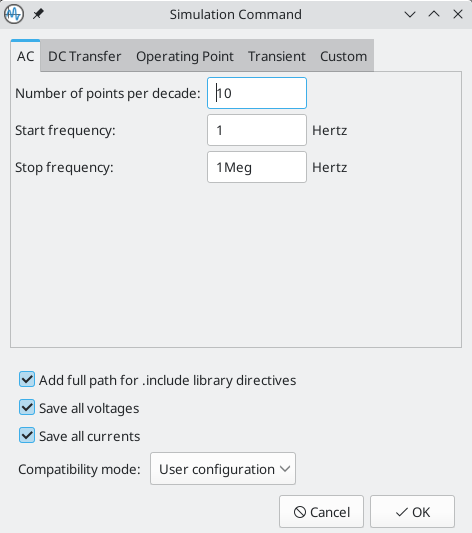
Calculates the small signal AC behavior of the circuit in response to a stimulus. Performs a decade sweep of stimulus frequency.
To run an AC analysis, you must choose a number of points to measure per decade and the start and end frequencies for the decade sweep.
The output is displayed as a Bode plot (output magnitude and phase vs. a decade sweep of stimulus frequency).
DC transfer analysis
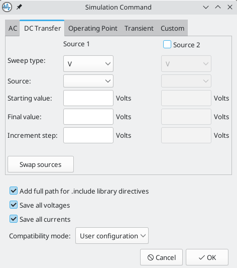
Calculates the DC behavior of the circuit while sweeping one or two sources (voltage or current), resistors, or the simulation temperature.
To run a DC analysis, you must choose what type of sweep(s) to perform, which source, resistor, or temperature value(s) to sweep, and what the sweep range(s) and step(s) should be.
The output is displayed as a plot.
Operating point analysis
Calculates the DC operating point of the circuit. This analysis has no options, and results are printed to the SPICE log.
Transient analysis
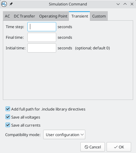
Calculates the time-varying behavior of the circuit.
To run a transient analysis, you need to specify a suggested time step and a final simulation time. You can optionally specify a starting time to override the default of 0.
The output is displayed as a plot.
Custom analysis
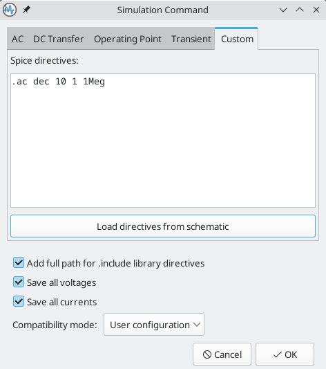
A custom analysis lets you write SPICE commands to set up the analysis. Press the Load directives from schematic button to copy any SPICE directives in schematic text into the custom analysis textbox.
Refer to the ngspice documentation for more information about analysis commands.
Additional simulation settings
There are several simulation options that apply to all types of simulations.
Add full path for .include library directives controls whether to convert
relative paths to absolute in .include directives in schematic text.
Save all voltages and Save all currents controls whether the simulator saves voltages and currents, respectively, for internal nodes of devices. When unchecked, the simulator only saves voltages and currents for external nodes.
The Compatibility mode dropdown selects the compatibility mode that the simulator uses to load models. The User configuration option refers to the user’s .spiceinit ngspice configuration file. Compatibility modes are described in the ngspice documentation.
Probing signals
Using the signal list
You can display a list of available signals with Simulation → Add signals (Ctrl+A hotkey or ![]() button). Double clicking an element in the list will add it to list of probed signals. Several signals can be selected at once using the Ctrl / Shift keys.
button). Double clicking an element in the list will add it to list of probed signals. Several signals can be selected at once using the Ctrl / Shift keys.
Using the probe tool
A probe tool is available in the toolbar of the simulator window (![]() ), which provides a user-friendly way of selecting signals for plotting. When activated, users can click elements in the schematic editor. To probe a voltage, click a wire with the probe tool. When hovering over wires with the tool, the corresponding net is highlighted. To probe a current, click on a symbol pin. When hovering over a pin, the cursor will change from a voltage probe symbol to a current clamp symbol. It is not possible to probe power signals with this tool.
), which provides a user-friendly way of selecting signals for plotting. When activated, users can click elements in the schematic editor. To probe a voltage, click a wire with the probe tool. When hovering over wires with the tool, the corresponding net is highlighted. To probe a current, click on a symbol pin. When hovering over a pin, the cursor will change from a voltage probe symbol to a current clamp symbol. It is not possible to probe power signals with this tool.
Using a SPICE directive
While ngspice supports the .plot directive, it cannot be used in current versions of KiCad.
Differential voltage
Probing differential voltages usually requires a simulation symbol. One is available in Simulation_SPICE:VOLTMETER_DIFF in the official libraries. This symbol has two terminals for differential voltage sensing, and one the user can probe.
A SPICE model called kicad_builtin_vdiff is preassigned to the built-in VOLTMETER_DIFF symbol. Users should not define a SPICE model with the same name.
|
It is also possible to probe across two-terminal devices such as a resistor by placing the .probe vd(X) directive, where X is the name of the device (such as R1). Then in order to probe it, enter vd_X when adding a signal using the list of signals. Note that the signal will not appear in the list of signals, it should be typed in by the user. This method has the advantage of not adding extra symbols to the schematic sheet.
Remove a signal probe
In order to remove a signal probe, double click on it in the signal list, or right-click it and select Remove Signal.
Tuning components
It is possible to change passive (R, L, C) values using sliders to graphically adjust them. Whenever the slider is set to a new position, the simulation is run with the new parameters and plots are updated. In order to add a slider for a component, use Simulation → Tune Component Value or the ![]() button in the toolbar, and then click on the component to tune.
button in the toolbar, and then click on the component to tune.
-
Il campo di testo in cima imposta il valore massimo del componente.
-
Il campo di testo di mezzo imposta il valore corrente del componente.
-
Il campo di testo in fondo imposta il valore minimo del componente.
-
The slider allows the user to modify the component value.
-
The Save button modifies component value on the schematic to the value selected with the slider.
-
The
 button removes the component from the Tune panel and restores its original value.
Visualizing results
Plotted quantities
This section applies to simulation commands that output vectors such as .ac and .tran.
Simulation results are visualized as plots. There can be multiple plots opened in separate tabs, but only the active one is updated when a simulation is executed. This way it is possible to compare simulation results for different runs.
Plots can be customized by toggling grid and legend visibility using the View menu. When a legend is visible, it can be dragged to change its position. You can toggle the plot background from dark to light with View → White Background and switch current and phase plots to use dotted lines instead of solid with View → Dotted Current/Phase.
For precise measurement, it is possible to add a cursor to a a signal. To do so, right click on a signal name in the Signals pane and select Show Cursor. It is then possible to move the cursor to the point of interest. The values are then shown in the Cursor section of the window. To hide a cursor, right click on a signal and select Hide Cursor. Each signal may have one cursor displayed.
The following interactions are possible with the plot panel:
-
la rotellina del mouse per ingrandire / rimpicciolire
-
clic destro per aprire il menu a scomparsa e regolare la visualizzazione
-
disegnare un rettangolo di selezione per fare lo zoom sull’area selezionata
-
trascinare un cursore per cambiarne le coordinate
Numerical values
Some analysis types, such as the DC operating point analysis (.op), do not have any graphical output to plot. Instead, their output is printed in the SPICE console.
Exporting results
KiCad’s simulator offers two ways to export results:
-
As an image using File → Export Current Plot as PNG…
-
As a
.csvfile containing the datapoints using File → Export Current Plot as CSV….
Troubleshooting
Incorrect netlist
It is possible to inspect the SPICE netlist with Simulation → Show SPICE netlist…. This method of troubleshooting requires some SPICE knowledge, but spotting errors in the netlist can help determine the cause of simulation problems.
Simulation error
The output console displays messages from the simulator. It is advised to check the console output to verify there are no errors or warnings.
Convergence problems
In case the simulation does not converge in a reasonable amount of time (or not at all), it is possible to add the following SPICE directives.
| Changing convergence options can lead to erroneous results. These options should be used with caution. |
.options gmin=1e-10
.options abstol=1e-10
.options reltol=0.003
.options cshunt=1e-15
-
gminis the minimum conductance allowed by the program. The default value is1e-12. -
abstolis the absolute current error tolerance of the program. The default value is 1 pA. -
reltolis the relative error tolerance of the program. The default value is0.001(0.1%). -
cshuntadds a capacitor from each voltage node in the circuit to ground.
Argomenti avanzati
Configurazione e personalizzazione
| Questa sezione della documentazione di KiCad non è stata ancora scritta. Pazientate: nel nostro piccolo team di documentazione volontaria gli autori lavorano quotidianamente per aggiornare ed espandere la documentazione. |
Variabili di testo
KiCad supports text variables, which allow you to substitute the variable name with a defined text string. This substitution happens anywhere the variable name is used inside the variable replacement syntax of ${VARIABLENAME}.
You can define your own text variables in the schematic or board setup dialogs, but there are also a number of built-in system text variables. System text variables may be available in some contexts and not others.
The following variables can be used in schematic text, label names, label fields, hierarchical sheet fields, symbol text, and symbol fields. There are also a number of variables that can be used in the PCB Editor.
Variables used in hierarchical sheet fields refer to the properties of the hierarchical sheet, not the parent, unless otherwise noted. For example, ${#} returns the subsheet’s page number when used in a hierarchical sheet field, but the parent sheet’s page number when used in graphic text in the parent sheet.
| Variable name | Description |
|---|---|
|
Sheet number. |
|
Total number of schematic sheets. |
|
Sheet path of the current sheet. |
|
Filename of the root schematic sheet, with a file extension. |
|
Project name, without a file extension. |
|
Contents of drawing sheet’s |
|
Today’s date, in ISO format. |
|
Contents of drawing sheet’s |
|
Contents of drawing sheet’s |
|
Contents of drawing sheet’s |
|
Contents of drawing sheet’s |
|
Contents of project text variable
|
|
Contents of symbol field, hierarchical sheet field, or label field
Both built-in and user-defined fields are available. Built-in fields use all
uppercase letters: for example, to access a symbol’s value, use Built-in symbol fields are Built-in sheet fields are Built-in label fields are |
|
Contents of field Both built-in and user-defined fields are available. Built-in fields use all
uppercase letters: for example, to access the value of Built-in symbol fields are |
Librerie di database
Una libreria di database è un tipo di libreria di simboli KiCad che contiene i dati sulle parti in un database SQL esterno. Le librerie di database non contengono di per sé definizioni di simboli o impronte. Invece, fanno riferimento a simboli e impronte trovati in altre librerie KiCad. Ogni voce della libreria del database mappa un simbolo KiCad (da un’altra libreria) a un insieme di proprietà (campi) e di solito un’impronta KiCad (da una libreria di impronte).
Using database libraries allows you to create fully-defined parts (sometimes called atomic parts) out of KiCad symbols and footprints without needing to store all the part properties in a symbol library. The external database can be linked to third-party tools for managing part data and lifecycles. Database library workflows are generally more complex than the standard KiCad library workflows, and so this type of library is typically only used in situations where it makes managing a large library of fully-defined parts more efficient (such as in organization or team settings).
KiCad does not provide a GUI for editing a SQL database or defining a database library. It is up to the user to find the most appropriate workflow and toolchain for creating and updating the database itself. Some users may want to directly edit the database through a third-party database client, and some may use other third-party software such as a part lifecycle management (PLM) tool to create and edit data.
In a database library, there are one or more tables that generally represent a single type of part (such as Resistors or Capacitors). Each table can have an independent schema, meaning that different types of parts can have different properties that are translated into symbol fields in KiCad. Each table must have a unique ID column which is used as the identifier for a symbol placed from that table. This unique ID will typically be a part number (either a manufacturer’s part number, or an internal organization part number). Each table must also have a column that contains a mapping to a KiCad symbol, in the form LibraryNickname:SymbolName. The LibraryNickname must match a symbol library that is present in the KiCad library tables. Tables may also contain a column containing a KiCad footprint, in the form LibraryNickname:FootprintName. If this column is present, symbols placed from the table will include a footprint mapping.
Tables may also contain arbitrary additional columns that may optionally be mapped to symbol fields in KiCad. The KiCad database library configuration file controls how these fields should be named, whether or not to make the fields visible, and whether or not to include the fields in the data displayed in the Symbol Chooser.
Database Library Configuration Files
To create a database library, you must create a configuration file that contains the necessary information for KiCad to connect to your database and retrieve data from tables. Copy the template below into a new file and save it with a kicad_dbl extension. You can then add this file to your global symbol library table using the Configure Symbol Libraries dialog.
{
    "meta": {
        "version": 0
    },
    "name": "My Database Library",
    "description": "A database of components",
    "source": {
        "type": "odbc",
        "dsn": "",
        "username": "",
        "password": "",
        "timeout_seconds": 2,
        "connection_string": ""
    },
    "libraries": [
        {
            "name": "Resistors",
            "table": "Resistors",
            "key": "Part ID",
            "symbols": "Symbols",
            "footprints": "Footprints",
            "fields": [
                {
                    "column": "MPN",
                    "name": "MPN",
                    "visible_on_add": false,
                    "visible_in_chooser": true,
                    "show_name": true,
                    "inherit_properties": true
                },
                {
                    "column": "Value",
                    "name": "Value",
                    "visible_on_add": true,
                    "visible_in_chooser": true,
                    "show_name": false
                }
            ],
            "properties": {
                "description": "Description",
                "footprint_filters": "Footprint Filters",
                "keywords": "Keywords",
                "exclude_from_bom": "No BOM",
                "exclude_from_board": "Schematic Only"
            }
        }
    ]
}
Configuring the source
KiCad currently only supports ODBC connections to SQL databases. You can either connect with a DSN or a connection string. If a DSN name is supplied, the optional username and password fields will be used to connect to the DSN. If a connection string is supplied, the dsn, username, and password fields are ignored. The connection string will be passed directly to the ODBC driver, so you can include any parameters your ODBC driver supports.
KiCad does not recommend or endorse any particular ODBC driver or database server, but has been tested to work with Sqlite, MySQL, MariaDB, and PostgreSQL.
Flatpak users: Due to Flatpak sandboxing, the only way to connect to database servers running on your local machine is via TCP/IP. Using the default UNIX domain socket connections for i.e. MySQL, MariaDB, or PostgreSQL is not possible. First, make sure that your database server allows TCP/IP connections, and then add the required Port parameter to your connection string. For example, add Port=3306; for the default TCP port of MySQL/MariaDB, or Server=localhost;Port=5432; to force PostgreSQL to use a TCP connection to the local server.
|
Configurazione delle librerie
Each database library can contain "sub-libraries" mapped to a single database table. The libraries entry in the configuration file contains a list of objects that each define a single library. The following settings must exist for each library:
name: The name of the table that will be shown in the KiCad UI.
table: The name of the table in the database.
key: The column name containing a unique key that will be used to identify parts from the table.
symbols: The column name containing KiCad symbol references.
footprints: The column name containing KiCad footprint references.
fields: A list of field definitions. Each field defined here will be added to the symbol when it is placed on the schematic. If a field with a matching name is already defined in the source symbol, the value from the database table will override whatever value was defined in the source symbol. Each field definition may contain:
column: The name of the database table column that should be mapped to a field.
name: The name of the KiCad field to populate from the database.
visible_on_add: If true, this field will be visible in the schematic when a symbol is added. If this setting is not specified, it will default to false.
visible_in_chooser: If true, this field will be shown in the Symbol Chooser as a column. If this setting is not specified, it will default to false.
show_name: If true, the field’s name will be shown in addition to its value in the schematic. If this setting is not specified, it will default to false.
inherit_properties: If true, and a field with the given name already exists on the source symbol, only the field contents will be updated from the database, and the other properties (visible_on_add, show_name, etc) will be kept as they were set in the source symbol. If the given field name does not exist in the source symbol, this setting is ignored. If this setting is not specified, it will default to false.
properties: A map of symbol properties to database columns. All properties are optional; any that are not specified in the database library configuration will be inherited from the values set for the source symbol. The following properties are supported:
description: The symbol’s Description property.
footprint_filters: Reserved for future expansion.
keywords: The symbol’s Keywords property.
exclude_from_bom: The symbol’s "Exclude from Bill of Materials" setting. The column named here must be a numeric type, and will be taken as a boolean (0 for false, 1 for true).
exclude_from_board: The symbol’s "Exclude from PCB" setting. The column named here must be a numeric type, and will be taken as a boolean (0 for false, 1 for true).
Database columns may be mapped to custom (user-defined) fields, or to certain built-in KiCad fields, including Value and Datasheet.
Using database libraries
After creating your configuration file and adding it to your symbol library table, you can place parts from the database tables using the Symbol Chooser. Parts placed from a database library can be updated using the Update Symbols from Library function, which will update any fields that were changed in the database as well as updating the underlying symbol if it was changed in the source library.
Note that any source library referenced by a database table must also be present in the symbol library table for the database library to function. If you want to use a library only as a source of symbols for a database library, you can hide it from the Symbol Chooser by clearing the "Visible" checkbox in the Manage Symbol Libraries dialog.
Netlist e DIBA personalizzate
KiCad può generare netlist e DIBA in vari formati e gli utenti possono definire nuovi formati se lo desiderano.
Il processo di esportazione di una netlist è descritto nella sezione esportazione netlist. Il risultato della DIBA è descritto nella sezione esportazione DIBA.
La sezione seguente descrive come creare un esportatore per un nuovo formato di uscita.
Aggiunta di nuovi generatori di netlist
I nuovi generatori di netlist vengono aggiunti alla finestra di dialogo Esporta netlist facendo clic sul pulsante Aggiungi generatore….
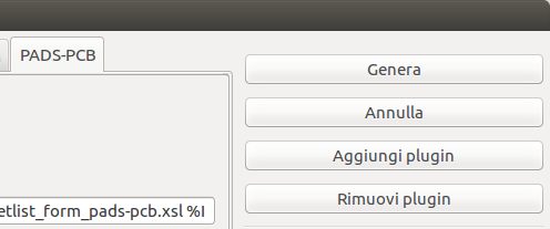
I nuovi generatori richiedono un nome e un comando. Il nome viene mostrato nell’etichetta della scheda e il comando viene eseguito ogni volta che si fa clic sul pulsante Esporta netlist.
Quando viene generata la netlist, KiCad crea un file XML intermedio che contiene tutte le informazioni della netlist dallo schema. In successione viene eseguito il comando generatore per trasformare la netlist intermedia nel formato netlist desiderato.
Il comando netlist deve essere impostato correttamente in modo che lo script del generatore di netlist prenda il file netlist intermedio come ingresso ed emetta il file netlist desiderato. L’esatto comando netlist dipenderà dallo script generatore utilizzato. Il formato del comando è descritto di seguito.
Python e XSLT sono strumenti comunemente usati per creare generatori di netlist personalizzate.
Aggiungere un nuovo generatore di DIBA
KiCad usa il file netlist intermedio anche per generare le distinte materiali con lo strumento generatore di DIBA.
Ulteriori script possono essere aggiunti all’elenco degli script del generatore DIBA facendo clic sul pulsante ![]() . Gli script possono essere rimossi facendo clic sul pulsante
. Gli script possono essere rimossi facendo clic sul pulsante ![]() . Il pulsante
. Il pulsante ![]() apre lo script selezionato in un editor di testo.
apre lo script selezionato in un editor di testo.
Gli script generatori in Python e XSLT possono contenere una intestazione di commento per descrivere funzione e uso del generatore. Questa intestazione di commento viene visualizzata nella finestra di dialogo DIBA come descrizione per ciascun generatore. L’intestazione di commento deve contenere la stringa @package. Tutto ciò che segue quella stringa fino alla fine del commento viene usato come descrizione per il generatore.
KiCad riempie automaticamente il campo della riga di comando quando viene aggiunto un nuovo script generatore, ma potrebbe essere necessario regolare manualmente la riga di comando a seconda dello script. KiCad tenta di determinare automaticamente l’estensione del file di output dalla riga di comando di esempio nell’intestazione dello script generatore.
Formato della linea di comando del generatore
La riga di comando per un esportatore di netlist o DIBA definisce il comando che KiCad eseguirà per generare il file di uscita selezionato.
Per un esportatore di netlist che utilizza xsltproc, un esempio è:
xsltproc -o %O.net /usr/share/kicad/plugins/netlist_form_pads-pcb.asc.xsl %I
Per un esportatore DIBA che usa Python, un esempio è:
/usr/bin/python3 /usr/share/kicad/plugins/bom_csv_grouped_by_value.py "%I" "%O.csv"
Si consiglia di racchiudere gli argomenti nella riga di comando tra virgolette (") nel caso in cui contengano spazi o altri caratteri speciali.
|
Alcune sequenze di caratteri come %I e %O hanno un significato speciale nella riga di comando, dato che KiCad le sostituisce con un nome file o un percorso prima di eseguire il comando.
| Parametro | Sostituito con… | Descrizione |
|---|---|---|
|
|
Percorso assoluto e nome file del file netlist intermedio, ingresso del plug-in DIBA o del generatore di netlist |
|
|
Percorso assoluto e nome file del file DIBA o netlist di uscita (senza estensione
file). Potrebbe essere necessario specificare un’estensione file appropriata dopo
la sequenza |
|
|
Nome file di base del file DIBA o netlist di uscita (senza percorso o estensione
file). Potrebbe essere necessario specificare un’estensione file appropriata dopo
la sequenza |
|
|
Percorso assoluto della cartella del progetto, senza barra finale. |
File di netlist intermedio
Quando si esportano file DIBA e netlist, KiCad crea un file netlist intermedio e quindi esegue uno strumento separato che post-elabora la netlist intermedia nel formato netlist o DIBA desiderato.
La netlist intermedia usa la sintassi XML. Essa contiene una grande quantità di dati sul progetto. A seconda del risultato (distinta materiali o netlist), differenti sottoinsiemi dell’intero file di netlist intermedia saranno inseriri nel file finale risultante.
La struttura del file della netlist intermedia è descritta in dettaglio sotto.
Poiché la conversione dal file della netlist intermedia alla netlist di uscita o DIBA è una trasformazione da testo a testo, il filtro di post-elaborazione può essere scritto utilizzando Python, XSLT o qualsiasi altro strumento in grado di accettare XML come ingresso.
XSLT non è raccomandato per nuovi esportatori di netlist o di DIBA; Meglio usare Python o un altro strumento. A partire da KiCad 7, xsltproc non è più installato con KiCad, sebbene possa essere installato separatamente. Tuttavia, di seguito sono inclusi diversi esempi di esportatori di netlist che usano XSLT.
|
Struttura netlist intermedia
Questo campione dà un’idea del formato del file netlist.
<?xml version="1.0" encoding="utf-8"?>
<export version="D">
  <design>
    <source>F:\kicad_aux\netlist_test\netlist_test.sch</source>
    <date>29/08/2010 21:07:51</date>
    <tool>eeschema (2010-08-28 BZR 2458)-unstable</tool>
  </design>
  <components>
    <comp ref="P1">
      <value>CONN_4</value>
      <libsource lib="conn" part="CONN_4"/>
      <sheetpath names="/" tstamps="/"/>
      <tstamps>4C6E2141</tstamps>
    </comp>
    <comp ref="U2">
      <value>74LS74</value>
      <libsource lib="74xx" part="74LS74"/>
      <sheetpath names="/" tstamps="/"/>
      <tstamps>4C6E20BA</tstamps>
    </comp>
    <comp ref="U1">
      <value>74LS04</value>
      <libsource lib="74xx" part="74LS04"/>
      <sheetpath names="/" tstamps="/"/>
      <tstamps>4C6E20A6</tstamps>
    </comp>
    <comp ref="C1">
      <value>CP</value>
      <libsource lib="device" part="CP"/>
      <sheetpath names="/" tstamps="/"/>
      <tstamps>4C6E2094</tstamps>
    <comp ref="R1">
      <value>R</value>
      <libsource lib="device" part="R"/>
      <sheetpath names="/" tstamps="/"/>
      <tstamps>4C6E208A</tstamps>
    </comp>
  </components>
  <libparts/>
  <libraries/>
  <nets>
    <net code="1" name="GND">
      <node ref="U1" pin="7"/>
      <node ref="C1" pin="2"/>
      <node ref="U2" pin="7"/>
      <node ref="P1" pin="4"/>
    </net>
    <net code="2" name="VCC">
      <node ref="R1" pin="1"/>
      <node ref="U1" pin="14"/>
      <node ref="U2" pin="4"/>
      <node ref="U2" pin="1"/>
      <node ref="U2" pin="14"/>
      <node ref="P1" pin="1"/>
    </net>
    <net code="3" name="">
      <node ref="U2" pin="6"/>
    </net>
    <net code="4" name="">
      <node ref="U1" pin="2"/>
      <node ref="U2" pin="3"/>
    </net>
    <net code="5" name="/SIG_OUT">
      <node ref="P1" pin="2"/>
      <node ref="U2" pin="5"/>
      <node ref="U2" pin="2"/>
    </net>
    <net code="6" name="/CLOCK_IN">
      <node ref="R1" pin="2"/>
      <node ref="C1" pin="1"/>
      <node ref="U1" pin="1"/>
      <node ref="P1" pin="3"/>
    </net>
  </nets>
</export>
Struttura generale del file netlist
La netlist intermedia consta di cinque sezioni.
-
La sezione intestazione.
-
La sezione componenti.
-
La sezione librerie di parti.
-
La sezione librerie.
-
La sezione collegamenti.
Il contenuto del file ha il delimitatore <export>
<export version="D">
...
</export>
Sezione intestazione
L’intestazione ha il delimitatore <design>
<design>
<source>F:\kicad_aux\netlist_test\netlist_test.sch</source>
<date>21/08/2010 08:12:08</date>
<tool>eeschema (2010-08-09 BZR 2439)-unstable</tool>
</design>
Questa sezione può essere considerata una sezione di commento.
La sezione componenti
La sezione componenti ha il delimitatore <components>
<components>
<comp ref="P1">
<value>CONN_4</value>
<libsource lib="conn" part="CONN_4"/>
<sheetpath names="/" tstamps="/"/>
<tstamps>4C6E2141</tstamps>
</comp>
</components>
Questa sezione contiene l’elenco componenti dello schema. Ogni componente viene descritto in questo modo:
<comp ref="P1">
<value>CONN_4</value>
<libsource lib="conn" part="CONN_4"/>
<sheetpath names="/" tstamps="/"/>
<tstamps>4C6E2141</tstamps>
</comp>| Nome elemento | Descrizione elemento |
|---|---|
|
nome della lib dove questo componente è stato trovato. |
|
nome componente dentro questa libreria. |
|
percorso del foglio dentro la gerarchia: identifica il foglio dentro la gerarchia generale dello schema. |
|
marcatura temporale del componente. |
Nota sulle marcature temporali per i componenti
Per identificare un componente in una netlist e quindi in una scheda, la marcatura temporale viene usata come riferimento univoco per ogni componente. Comunque KiCad fornisce un modo alternativo per identificare il corrispondente componente di una impronta sulla scheda. Ciò permette la ri-annotazione di componenti in un progetto di schema elettrico non perdendo il collegamento tra il componente e la sua impronta.
Un marcatore temporale è un identificatore univoco per ogni componente o foglio in un progetto di schema elettrico. Ma in caso di gerarchie complesse, lo stesso foglio viene usato più di una volta, perciò il foglio contiene componenti aventi la stessa marcatura temporale.
Un dato foglio dentro una gerarchia complessa possiede un identificatore univoco: il suo percorso foglio. Un dato componente (dentro una gerarchia complessa) possiede un identificativo univoco: il percorso foglio + la sua marcatura temporale.
La sezione libparts
La sezione libparts ha un delimitatore <libparts>, e il contenuto di questa sezione viene definito nelle librerie degli schemi.
<libparts>
<libpart lib="device" part="CP">
  <description>Condensatore polarizzato</description>
  <footprints>
    <fp>CP*</fp>
    <fp>SM*</fp>
  </footprints>
  <fields>
    <field name="Riferimento">C</field>
    <field name="Valore">CP</field>
  </fields>
  <pins>
    <pin num="1" name="1" type="passive"/>
    <pin num="2" name="2" type="passive"/>
  </pins>
</libpart>
</libparts>| Nome elemento | Descrizione elemento |
|---|---|
|
I filtri impronte del simbolo. Ogni filtro impronta si trova in un marcatore |
|
I campi del simbolo. Il nome e il valore di ciascun campo sono dati in un marcatore `<field name="nomecampo">…</field> separato. |
|
I pin del simbolo. Ogni pin è fornito in un marcatore |
Tipi elettrici dei pin possibili sono:
| Tipopin | Descrizione |
|---|---|
Input |
Normale pin di ingresso |
Output |
Normale pin di uscita |
Bidirectional |
Ingresso o uscita |
Tri-state |
Bus ingresso/uscita |
Passive |
Normale capo di componente passivo |
Unspecified |
Tipo elettrico sconosciuto |
Power input |
Ingresso di potenza, per es. l’alimentazione di un componente |
Power output |
Uscita di potenza, per es. l’uscita di regolatore di tensione |
Open collector |
Collettore aperto, comune dei comparatori analogici |
Open emitter |
Emettitore aperto, presente in alcuni circuiti logici |
Not connected |
Deve essere lasciato aperto nello schema elettrico |
La sezione librerie
La sezione librerie possiede il delimitatore <libraries>. Questa sezione contiene l’elenco delle librerie di schemi elettrici usate nel progetto.
<libraries>
  <library logical="device">
    <uri>F:\kicad\share\library\device.lib</uri>
  </library>
  <library logical="conn">
    <uri>F:\kicad\share\library\conn.lib</uri>
  </library>
</libraries>
La sezione collegamenti
La sezione net possiede il delimitatore <nets>. Questa sezione contiene le connessioni dello schema elettrico elencando tutte le net e i pin connessi ad esse.
<nets>
  <net code="1" name="GND">
    <node ref="U1" pin="7"/>
    <node ref="C1" pin="2"/>
    <node ref="U2" pin="7"/>
    <node ref="P1" pin="4"/>
  </net>
  <net code="2" name="VCC">
    <node ref="R1" pin="1"/>
    <node ref="U1" pin="14"/>
    <node ref="U2" pin="4"/>
    <node ref="U2" pin="1"/>
    <node ref="U2" pin="14"/>
    <node ref="P1" pin="1"/>
  </net>
</nets>
Un tipico collegamento contiene i seguenti elementi.
<net code="1" name="GND">
  <node ref="U1" pin="7"/>
  <node ref="C1" pin="2"/>
  <node ref="U2" pin="7"/>
  <node ref="P1" pin="4"/>
</net>| Nome elemento | Descrizione elemento |
|---|---|
|
un identificatore interno per questa net |
|
il nome collegamento |
|
il piedino (identificato da |
Esportatori di netlist di esempio
Alcuni esportatori di netlist di esempio che usano XSLT sono inclusi sotto.
XSLT è di per sè un linguaggio XML molto adatto alle trasformazioni XML. Il programma xsltproc può essere usato per leggere in ingresso il file XML di netlist intermedio, applicare un foglio di stile per trasformare l’ingresso, e salvare il risultato in un file in uscita. L’uso di xsltproc richiede un file foglio di stile che usi le convenzioni XSLT. L’intero processo di conversione viene gestito da KiCad, dopo essere stato configurato per l’esecuzione di xsltproc in modo specifico.
Il documento che descrive le trasformazioni XSL (XSLT) è disponibile qui: http://www.w3.org/TR/xslt
| Quando si sta scrivendo un nuovo esportatore di netlist, si consiglia di prendere in considerazione l’uso di Python o di un altro linguaggio ad alto livello al posto di XSLT. |
Esempio di netlist PADS usando XSLT
L’esempio seguente mostra come creare un esportatore per il formato netlist PADS utilizzando xlstproc.
Il formato netlist di PADS è formato da due sezioni:
-
Un elenco di impronte
-
Un elenco di net, assieme con le piazzole connesse ad ogni net.
Immediatamente di seguito c’è un foglio di stile XSL che converte il file di netlist intermedio in formato netlist PADS.
<?xml version="1.0" encoding="ISO-8859-1"?>
<!--XSL style sheet to Eeschema Generic Netlist Format to PADS netlist format
Copyright (C) 2010, SoftPLC Corporation.
GPL v2.
How to use:
https://lists.launchpad.net/kicad-developers/msg05157.html
-->
<!DOCTYPE xsl:stylesheet [
<!ENTITY nl "
"> <!--new line CR, LF -->
]>
<xsl:stylesheet version="1.0" xmlns:xsl="http://www.w3.org/1999/XSL/Transform">
<xsl:output method="text" omit-xml-declaration="yes" indent="no"/>
<xsl:template match="/export">
<xsl:text>*PADS-PCB*&nl;*PART*&nl;</xsl:text>
<xsl:apply-templates select="components/comp"/>
<xsl:text>&nl;*NET*&nl;</xsl:text>
<xsl:apply-templates select="nets/net"/>
<xsl:text>*END*&nl;</xsl:text>
</xsl:template>
<!-- per ogni componente -->
<xsl:template match="comp">
<xsl:text> </xsl:text>
<xsl:value-of select="@ref"/>
<xsl:text> </xsl:text>
<xsl:choose>
<xsl:when test = "footprint != '' ">
<xsl:apply-templates select="footprint"/>
</xsl:when>
<xsl:otherwise>
<xsl:text>unknown</xsl:text>
</xsl:otherwise>
</xsl:choose>
<xsl:text>&nl;</xsl:text>
</xsl:template>
<!-- per ogni net -->
<xsl:template match="net">
<!-- nets are output only if there is more than one pin in net -->
<xsl:if test="count(node)>1">
<xsl:text>*SIGNAL* </xsl:text>
<xsl:choose>
<xsl:when test = "@name != '' ">
<xsl:value-of select="@name"/>
</xsl:when>
<xsl:otherwise>
<xsl:text>N-</xsl:text>
<xsl:value-of select="@code"/>
</xsl:otherwise>
</xsl:choose>
<xsl:text>&nl;</xsl:text>
<xsl:apply-templates select="node"/>
</xsl:if>
</xsl:template>
<!-- per ogni nodo -->
<xsl:template match="node">
<xsl:text> </xsl:text>
<xsl:value-of select="@ref"/>
<xsl:text>.</xsl:text>
<xsl:value-of select="@pin"/>
<xsl:text>&nl;</xsl:text>
</xsl:template>
</xsl:stylesheet>Ed ecco il file netlist PADS in uscita dopo l’esecuzione di xsltproc:
*PADS-PCB*
*PART*
P1 unknown
U2 unknown
U1 unknown
C1 unknown
R1 unknown
*NET*
*SIGNAL* GND
U1.7
C1.2
U2.7
P1.4
*SIGNAL* VCC
R1.1
U1.14
U2.4
U2.1
U2.14
P1.1
*SIGNAL* N-4
U1.2
U2.3
*SIGNAL* /SIG_OUT
P1.2
U2.5
U2.2
*SIGNAL* /CLOCK_IN
R1.2
C1.1
U1.1
P1.3

*END*
La riga di comando per effettuare questa conversione è:
kicad\\bin\\xsltproc.exe -o test.net kicad\\bin\\plugins\\netlist_form_pads-pcb.xsl test.tmp
Esempio di netlist Cadstar usando XSLT
L’esempio seguente mostra come creare un esportatore per il formato netlist Cadstar usando xlstproc.
Il formato Cadstar è formato da due sezioni:
-
L’elenco impronte
-
La netslist: raggruppando riferimenti a piazzole per collegamenti
Di seguito c’è un foglio di stile XSL che converte il file di netlist intermedio in formato netlist Cadstar.
<?xml version="1.0" encoding="ISO-8859-1"?>
<!--XSL style sheet to Eeschema Generic Netlist Format to CADSTAR netlist format
Copyright (C) 2010, Jean-Pierre Charras.
Copyright (C) 2010, SoftPLC Corporation.
GPL v2. -->
<!DOCTYPE xsl:stylesheet [
<!ENTITY nl "
"> <!--new line CR, LF -->
]>
<xsl:stylesheet version="1.0" xmlns:xsl="http://www.w3.org/1999/XSL/Transform">
<xsl:output method="text" omit-xml-declaration="yes" indent="no"/>
<!-- Netlist header -->
<xsl:template match="/export">
<xsl:text>.HEA&nl;</xsl:text>
<xsl:apply-templates select="design/date"/> <!-- Generate line .TIM <time> -->
<xsl:apply-templates select="design/tool"/> <!-- Generate line .APP <eeschema version> -->
<xsl:apply-templates select="components/comp"/> <!-- Generate list of components -->
<xsl:text>&nl;&nl;</xsl:text>
<xsl:apply-templates select="nets/net"/> <!-- Generate list of nets and connections -->
<xsl:text>&nl;.END&nl;</xsl:text>
</xsl:template>
<!-- Generate line .TIM 20/08/2010 10:45:33 -->
<xsl:template match="tool">
<xsl:text>.APP "</xsl:text>
<xsl:apply-templates/>
<xsl:text>"&nl;</xsl:text>
</xsl:template>
<!-- Generate line .APP "eeschema (2010-08-17 BZR 2450)-unstable" -->
<xsl:template match="date">
<xsl:text>.TIM </xsl:text>
<xsl:apply-templates/>
<xsl:text>&nl;</xsl:text>
</xsl:template>
<!-- for each component -->
<xsl:template match="comp">
<xsl:text>.ADD_COM </xsl:text>
<xsl:value-of select="@ref"/>
<xsl:text> </xsl:text>
<xsl:choose>
<xsl:when test = "value != '' ">
<xsl:text>"</xsl:text> <xsl:apply-templates select="value"/> <xsl:text>"</xsl:text>
</xsl:when>
<xsl:otherwise>
<xsl:text>""</xsl:text>
</xsl:otherwise>
</xsl:choose>
<xsl:text>&nl;</xsl:text>
</xsl:template>
<!-- for each net -->
<xsl:template match="net">
<!-- nets are output only if there is more than one pin in net -->
<xsl:if test="count(node)>1">
<xsl:variable name="netname">
<xsl:text>"</xsl:text>
<xsl:choose>
<xsl:when test = "@name != '' ">
<xsl:value-of select="@name"/>
</xsl:when>
<xsl:otherwise>
<xsl:text>N-</xsl:text>
<xsl:value-of select="@code"/>
</xsl:otherwise>
</xsl:choose>
<xsl:text>"&nl;</xsl:text>
</xsl:variable>
<xsl:apply-templates select="node" mode="first"/>
<xsl:value-of select="$netname"/>
<xsl:apply-templates select="node" mode="others"/>
</xsl:if>
</xsl:template>
<!-- for each node -->
<xsl:template match="node" mode="first">
<xsl:if test="position()=1">
<xsl:text>.ADD_TER </xsl:text>
<xsl:value-of select="@ref"/>
<xsl:text>.</xsl:text>
<xsl:value-of select="@pin"/>
<xsl:text> </xsl:text>
</xsl:if>
</xsl:template>
<xsl:template match="node" mode="others">
<xsl:choose>
<xsl:when test='position()=1'>
</xsl:when>
<xsl:when test='position()=2'>
<xsl:text>.TER </xsl:text>
</xsl:when>
<xsl:otherwise>
<xsl:text> </xsl:text>
</xsl:otherwise>
</xsl:choose>
<xsl:if test="position()>1">
<xsl:value-of select="@ref"/>
<xsl:text>.</xsl:text>
<xsl:value-of select="@pin"/>
<xsl:text>&nl;</xsl:text>
</xsl:if>
</xsl:template>
</xsl:stylesheet>Ecco il file Cadstar in uscita.
.HEA
.TIM 21/08/2010 08:12:08
.APP "eeschema (2010-08-09 BZR 2439)-unstable"
.ADD_COM P1 "CONN_4"
.ADD_COM U2 "74LS74"
.ADD_COM U1 "74LS04"
.ADD_COM C1 "CP"
.ADD_COM R1 "R"


.ADD_TER U1.7 "GND"
.TER     C1.2
         U2.7
         P1.4
.ADD_TER R1.1 "VCC"
.TER     U1.14
         U2.4
         U2.1
         U2.14
         P1.1
.ADD_TER U1.2 "N-4"
.TER     U2.3
.ADD_TER P1.2 "/SIG_OUT"
.TER     U2.5
         U2.2
.ADD_TER R1.2 "/CLOCK_IN"
.TER     C1.1
         U1.1
         P1.3

.END
Esempio di netlist di OrcadPCB2 che usa XSLT
Questo formato ha solo una sezione che consiste nell’elenco impronte. Ogni impronta include un elenco piazzole con un riferimento ad una connessione.
Di seguito c’è un foglio di stile XSL che converte il file di netlist intermedio in formato netlist Orcad.
<?xml version="1.0" encoding="ISO-8859-1"?>
<!--XSL style sheet to Eeschema Generic Netlist Format to CADSTAR netlist format
Copyright (C) 2010, SoftPLC Corporation.
GPL v2.
How to use:
https://lists.launchpad.net/kicad-developers/msg05157.html
-->
<!DOCTYPE xsl:stylesheet [
<!ENTITY nl "
"> <!--new line CR, LF -->
]>
<xsl:stylesheet version="1.0" xmlns:xsl="http://www.w3.org/1999/XSL/Transform">
<xsl:output method="text" omit-xml-declaration="yes" indent="no"/>
<!--
Netlist header
Creates the entire netlist
(can be seen as equivalent to main function in C
-->
<xsl:template match="/export">
<xsl:text>( { Eeschema Netlist Version 1.1 </xsl:text>
<!-- Generate line .TIM <time> -->
<xsl:apply-templates select="design/date"/>
<!-- Generate line eeschema version ... -->
<xsl:apply-templates select="design/tool"/>
<xsl:text>}&nl;</xsl:text>
<!-- Generate the list of components -->
<xsl:apply-templates select="components/comp"/> <!-- Generate list of components -->
<!-- end of file -->
<xsl:text>)&nl;*&nl;</xsl:text>
</xsl:template>
<!--
Generate id in header like "eeschema (2010-08-17 BZR 2450)-unstable"
-->
<xsl:template match="tool">
<xsl:apply-templates/>
</xsl:template>
<!--
Generate date in header like "20/08/2010 10:45:33"
-->
<xsl:template match="date">
<xsl:apply-templates/>
<xsl:text>&nl;</xsl:text>
</xsl:template>
<!--
This template read each component
(path = /export/components/comp)
creates lines:
( 3EBF7DBD $noname U1 74LS125
... pin list ...
)
and calls "create_pin_list" template to build the pin list
-->
<xsl:template match="comp">
<xsl:text> ( </xsl:text>
<xsl:choose>
<xsl:when test = "tstamp != '' ">
<xsl:apply-templates select="tstamp"/>
</xsl:when>
<xsl:otherwise>
<xsl:text>00000000</xsl:text>
</xsl:otherwise>
</xsl:choose>
<xsl:text> </xsl:text>
<xsl:choose>
<xsl:when test = "footprint != '' ">
<xsl:apply-templates select="footprint"/>
</xsl:when>
<xsl:otherwise>
<xsl:text>$noname</xsl:text>
</xsl:otherwise>
</xsl:choose>
<xsl:text> </xsl:text>
<xsl:value-of select="@ref"/>
<xsl:text> </xsl:text>
<xsl:choose>
<xsl:when test = "value != '' ">
<xsl:apply-templates select="value"/>
</xsl:when>
<xsl:otherwise>
<xsl:text>"~"</xsl:text>
</xsl:otherwise>
</xsl:choose>
<xsl:text>&nl;</xsl:text>
<xsl:call-template name="Search_pin_list" >
<xsl:with-param name="cmplib_id" select="libsource/@part"/>
<xsl:with-param name="cmp_ref" select="@ref"/>
</xsl:call-template>
<xsl:text> )&nl;</xsl:text>
</xsl:template>
<!--
This template search for a given lib component description in list
lib component descriptions are in /export/libparts,
and each description start at ./libpart
We search here for the list of pins of the given component
This template has 2 parameters:
"cmplib_id" (reference in libparts)
"cmp_ref" (schematic reference of the given component)
-->
<xsl:template name="Search_pin_list" >
<xsl:param name="cmplib_id" select="0" />
<xsl:param name="cmp_ref" select="0" />
<xsl:for-each select="/export/libparts/libpart">
<xsl:if test = "@part = $cmplib_id ">
<xsl:apply-templates name="build_pin_list" select="pins/pin">
<xsl:with-param name="cmp_ref" select="$cmp_ref"/>
</xsl:apply-templates>
</xsl:if>
</xsl:for-each>
</xsl:template>
<!--
This template writes the pin list of a component
from the pin list of the library description
The pin list from library description is something like
<pins>
<pin num="1" type="passive"/>
<pin num="2" type="passive"/>
</pins>
Output pin list is ( <pin num> <net name> )
something like
( 1 VCC )
( 2 GND )
-->
<xsl:template name="build_pin_list" match="pin">
<xsl:param name="cmp_ref" select="0" />
<!-- write pin numner and separator -->
<xsl:text> ( </xsl:text>
<xsl:value-of select="@num"/>
<xsl:text> </xsl:text>
<!-- search net name in nets section and write it: -->
<xsl:variable name="pinNum" select="@num" />
<xsl:for-each select="/export/nets/net">
<!-- net name is output only if there is more than one pin in net
else use "?" as net name, so count items in this net
-->
<xsl:variable name="pinCnt" select="count(node)" />
<xsl:apply-templates name="Search_pin_netname" select="node">
<xsl:with-param name="cmp_ref" select="$cmp_ref"/>
<xsl:with-param name="pin_cnt_in_net" select="$pinCnt"/>
<xsl:with-param name="pin_num"> <xsl:value-of select="$pinNum"/>
</xsl:with-param>
</xsl:apply-templates>
</xsl:for-each>
<!-- close line -->
<xsl:text> )&nl;</xsl:text>
</xsl:template>
<!--
This template writes the pin netname of a given pin of a given component
from the nets list
The nets list description is something like
<nets>
<net code="1" name="GND">
<node ref="J1" pin="20"/>
<node ref="C2" pin="2"/>
</net>
<net code="2" name="">
<node ref="U2" pin="11"/>
</net>
</nets>
This template has 2 parameters:
"cmp_ref" (schematic reference of the given component)
"pin_num" (pin number)
-->
<xsl:template name="Search_pin_netname" match="node">
<xsl:param name="cmp_ref" select="0" />
<xsl:param name="pin_num" select="0" />
<xsl:param name="pin_cnt_in_net" select="0" />
<xsl:if test = "@ref = $cmp_ref ">
<xsl:if test = "@pin = $pin_num">
<!-- net name is output only if there is more than one pin in net
else use "?" as net name
-->
<xsl:if test = "$pin_cnt_in_net>1">
<xsl:choose>
<!-- if a net has a name, use it,
else build a name from its net code
-->
<xsl:when test = "../@name != '' ">
<xsl:value-of select="../@name"/>
</xsl:when>
<xsl:otherwise>
<xsl:text>$N-0</xsl:text><xsl:value-of select="../@code"/>
</xsl:otherwise>
</xsl:choose>
</xsl:if>
<xsl:if test = "$pin_cnt_in_net <2">
<xsl:text>?</xsl:text>
</xsl:if>
</xsl:if>
</xsl:if>
</xsl:template>
</xsl:stylesheet>Ecco il file OrcadPCB2 risultante.
( { Eeschema Netlist Version 1.1  29/08/2010 21:07:51
eeschema (2010-08-28 BZR 2458)-unstable}
 ( 4C6E2141 $noname P1 CONN_4
  (  1 VCC )
  (  2 /SIG_OUT )
  (  3 /CLOCK_IN )
  (  4 GND )
 )
 ( 4C6E20BA $noname U2 74LS74
  (  1 VCC )
  (  2 /SIG_OUT )
  (  3 N-04 )
  (  4 VCC )
  (  5 /SIG_OUT )
  (  6 ? )
  (  7 GND )
  (  14 VCC )
 )
 ( 4C6E20A6 $noname U1 74LS04
  (  1 /CLOCK_IN )
  (  2 N-04 )
  (  7 GND )
  (  14 VCC )
 )
 ( 4C6E2094 $noname C1 CP
  (  1 /CLOCK_IN )
  (  2 GND )
 )
 ( 4C6E208A $noname R1 R
  (  1 VCC )
  (  2 /CLOCK_IN )
 )
)
*
Riferimento azioni
Di seguito è riportato un elenco di ogni azione disponibile nell’editor degli schemi elettrici di KiCad: un comando che può essere assegnato a un tasto comando.
Editor degli schemi elettrici
Le azioni seguenti sono disponibili nell’editor degli schemi elettrici. I tasti di scelta rapida possono essere assegnati a una qualsiasi di queste azioni nella sezione Tasti comando delle preferenze.
| Action | Default Hotkey | Description |
|---|---|---|
Align Elements to Grid |
||
Annotate Schematic… |
Fill in schematic symbol reference designators |
|
Annotate Automatically |
Toggle automatic annotation of new parts symbols |
|
Assign Footprints… |
Run footprint assignment tool |
|
Clear Net Highlighting |
~ |
Clear any existing net highlighting |
Export Drawing to Clipboard |
Export drawing of current sheet to clipboard |
|
Edit Library Symbol… |
Ctrl+Shift+E |
Open the library symbol in the Symbol Editor |
Edit Sheet Page Number… |
Edit the page number of the current or selected sheet |
|
Edit Symbol Fields… |
Bulk-edit fields of all symbols in schematic |
|
Edit Symbol Library Links… |
Edit links between schematic and library symbols |
|
Edit with Symbol Editor |
Ctrl+E |
Open the selected symbol in the Symbol Editor |
Export Netlist… |
Export file containing netlist in one of several formats |
|
Export Symbols to Library… |
Add symbols used in schematic to an existing symbol library (does not remove other symbols from this library) |
|
Export Symbols to New Library… |
Create a new symbol library using the symbols used in the schematic (if the library already exists it will be replaced) |
|
Generate BOM… |
Generate a bill of materials for the current schematic |
|
Highlight Net |
` |
Highlight net under cursor |
Highlight Nets |
Highlight wires and pins of a net |
|
Import Footprint Assignments… |
Import symbol footprint assignments from .cmp file created by board editor |
|
Line Mode for Wires and Buses |
Constrain drawing and dragging to horizontal, vertical, or 45-degree angle motions |
|
Line Mode for Wires and Buses |
Draw and drag at any angle |
|
Line Mode for Wires and Buses |
Shift+Space |
Switch to next line mode |
Line Mode for Wires and Buses |
Constrain drawing and dragging to horizontal or vertical motions |
|
Remap Legacy Library Symbols… |
Remap library symbol references in legacy schematics to the symbol library table |
|
Repair Schematic |
Run various diagnostics and attempt to repair schematic |
|
Rescue Symbols… |
Find old symbols in project and rename/rescue them |
|
Simulator… |
Simulate circuit in SPICE |
|
Save Current Sheet Copy As… |
Save a copy of the current sheet to another location or name |
|
Schematic Setup… |
Edit schematic setup including annotation styles and electrical rules |
|
Select on PCB |
Select corresponding items in PCB editor |
|
Show ERC Errors |
Show markers for electrical rules checker errors |
|
Show ERC Exclusions |
Show markers for excluded electrical rules checker violations |
|
Show ERC Warnings |
Show markers for electrical rules checker warnings |
|
Show Hidden Fields |
Toggle display of hidden text fields |
|
Show Hidden Pins |
Toggle display of hidden pins |
|
Switch to PCB Editor |
Open PCB in board editor |
|
Scripting Console |
Show the Python scripting console |
|
Hierarchy Navigator |
Ctrl+H |
Show or hide the schematic sheet hierarchy navigator |
Symbol Checker |
Show the symbol checker window |
|
Electrical Rules Checker |
Perform electrical rules check |
|
Show Datasheet |
D |
Opens the datasheet in a browser |
Add Arc |
Add an arc |
|
Add Circle |
Add a circle |
|
Add Rectangle |
Add a rectangle |
|
Add Sheet |
S |
Add a hierarchical sheet |
Add Text Box |
Add a text box |
|
Finish Sheet |
Finish drawing sheet |
|
Import Sheet Pin |
Import a hierarchical sheet pin |
|
Add Wire to Bus Entry |
Z |
Add a wire entry to a bus |
Add Net Class Directive |
Add a net class directive label |
|
Add Global Label |
Ctrl+L |
Add a global label |
Add Hierarchical Label |
H |
Add a hierarchical label |
Add Image |
Add bitmap image |
|
Add Junction |
J |
Add a junction |
Add Label |
L |
Add a net label |
Add No Connect Flag |
Q |
Add a no-connection flag |
Add Power |
P |
Add a power symbol |
Add Text |
T |
Add text |
Add Symbol |
A |
Add a symbol |
Add Bus |
B |
Add a bus |
Add Lines |
I |
Add connected graphic lines |
Add Wire |
W |
Add a wire |
Finish Wire or Bus |
K |
Complete drawing at current segment |
Finish Bus |
Complete bus with current segment |
|
Finish Lines |
Complete connected lines with current segment |
|
Finish Wire |
Complete wire with current segment |
|
Switch Segment Posture |
/ |
Switches posture of the current segment. |
Undo Last Segment |
Back |
Walks the current line back one segment. |
Unfold from Bus |
C |
Break a wire out of a bus |
Assign Netclass… |
Assign a netclass to nets matching a pattern |
|
Autoplace Fields |
O |
Runs the automatic placement algorithm on the symbol or sheet’s fields |
Break |
Divide into connected segments |
|
Change Symbol… |
Assign a different symbol from the library |
|
Change Symbols… |
Assign different symbols from the library |
|
Cleanup Sheet Pins |
Delete unreferenced sheet pins |
|
Edit Footprint… |
F |
Displays footprint field dialog |
Edit Reference Designator… |
U |
Displays reference designator dialog |
Edit Text & Graphics Properties… |
Edit text and graphics properties globally across schematic |
|
Edit Value… |
V |
Displays value field dialog |
Mirror Horizontally |
X |
Flips selected item(s) from left to right |
Mirror Vertically |
Y |
Flips selected item(s) from top to bottom |
Pin Table… |
Displays pin table for bulk editing of pins |
|
Properties… |
E |
Displays item properties dialog |
Repeat Last Item |
Ins |
Duplicates the last drawn item |
Rotate Counterclockwise |
R |
Rotates selected item(s) counter-clockwise |
Rotate Clockwise |
Rotates selected item(s) clockwise |
|
De Morgan Alternate |
Switch to alternate De Morgan representation |
|
De Morgan Standard |
Switch to standard De Morgan representation |
|
Slice |
Divide into unconnected segments |
|
Swap |
Shift+S |
Swaps selected items' positions |
Symbol Properties… |
Displays symbol properties dialog |
|
Change to Directive Label |
Change existing item to a directive label |
|
Change to Global Label |
Change existing item to a global label |
|
Change to Hierarchical Label |
Change existing item to a hierarchical label |
|
Change to Label |
Change existing item to a label |
|
Change to Text |
Change existing item to a text comment |
|
Change to Text Box |
Change existing item to a text box |
|
De Morgan Conversion |
Switch between De Morgan representations |
|
Update Symbol… |
Update symbol to include any changes from the library |
|
Update Symbols from Library… |
Update symbols to include any changes from the library |
|
Move Activate |
||
Drag |
G |
Drags the selected item(s) |
Move |
M |
Moves the selected item(s) |
Select Connection |
Alt+4 |
Select a complete connection |
Select Node |
Alt+3 |
Select a connection item under the cursor |
Navigate Back |
Alt+Left |
Move backward in sheet navigation history |
Change Sheet |
Change to provided sheet’s contents in the schematic editor |
|
Enter Sheet |
Display the selected sheet’s contents in the schematic editor |
|
Navigate Forward |
Alt+Right |
Move forward in sheet navigation history |
Leave Sheet |
Alt+Back |
Display the parent sheet in the schematic editor |
Next Sheet |
PgDn |
Move to next sheet by number |
Previous Sheet |
PgUp |
Move to previous sheet by number |
Navigate Up |
Alt+Up |
Navigate up one sheet in the hierarchy |
Push Pin Length |
Copy pin length to other pins in symbol |
|
Push Pin Name Size |
Copy pin name size to other pins in symbol |
|
Push Pin Number Size |
Copy pin number size to other pins in symbol |
|
Create Corner |
Create a corner |
|
Remove Corner |
Remove corner |
|
Add a simulator probe |
||
Select a value to be tuned |
||
Add Lines |
Add connected graphic lines |
|
Add Text Box |
Add a text box item |
|
Finish Drawing |
Finish drawing shape |
|
Move Symbol Anchor |
Specify a new location for the symbol anchor |
|
Add Pin |
P |
Add a pin |
Add Text |
Add a text item |
|
Add Symbol to Schematic |
Add Symbol to Schematic |
|
Copy |
||
Cut |
||
Delete Symbol |
Remove the selected symbol from its library |
|
Duplicate Symbol |
Make a copy of the selected symbol |
|
Edit Symbol |
Show selected symbol on editor canvas |
|
Export… |
Export a symbol to a new library file |
|
Export Symbol as SVG… |
Create SVG file from the current symbol |
|
Export View as PNG… |
Create PNG file from the current view |
|
Hide Symbol Tree |
||
Import Symbol… |
Import a symbol to the current library |
|
New Symbol… |
N |
Create a new symbol |
Paste Symbol |
||
Rename Symbol… |
Rename the selected symbol |
|
Save Library As… |
Ctrl+Shift+S |
Save the current library to a new file. |
Save As… |
Save the current symbol to a different library. |
|
Set Unit Display Name… |
Set the display name for a unit |
|
Show Pin Electrical Types |
Annotate pins with their electrical types |
|
Show Pin Numbers |
Annotate pins with their numbers |
|
Show Symbol Tree |
||
Synchronized Pins Mode |
Synchronized Pins Mode When enabled propagates all changes (except pin numbers) to other units. Enabled by default for multiunit parts with interchangeable units. |
|
Update Symbol Fields… |
Update symbol to match changes made in parent symbol |
|
Symbol Move Activate |
Comuni
Le azioni seguenti sono disponibili in KiCad, incluso nell’editor degli schemi. I tasti comando possono essere assegnati a una qualsiasi di queste azioni nella sezione Tasti comando delle preferenze.
| Action | Default Hotkey | Description |
|---|---|---|
Exclude Marker |
Mark current violation in Checker window as an exclusion |
|
Next Marker |
Go to next marker in Checker window |
|
Previous Marker |
Go to previous marker in Checker window |
|
Add Library… |
Add an existing library folder |
|
Click |
Return |
Performs left mouse button click |
Double-click |
End |
Performs left mouse button double-click |
Cursor Down |
Down |
|
Cursor Down Fast |
Ctrl+Down |
|
Cursor Left |
Left |
|
Cursor Left Fast |
Ctrl+Left |
|
Cursor Right |
Right |
|
Cursor Right Fast |
Ctrl+Right |
|
Cursor Up |
Up |
|
Cursor Up Fast |
Ctrl+Up |
|
Switch to Fast Grid 1 |
Alt+1 |
|
Switch to Fast Grid 2 |
Alt+2 |
|
Switch to Next Grid |
N |
|
Switch to Previous Grid |
Shift+N |
|
Grid Properties… |
Set grid dimensions |
|
Reset Grid Origin |
Z |
|
Grid Origin |
S |
Set the grid origin point |
Inactive Layer View Mode |
Toggle inactive layers between normal and dimmed |
|
Inactive Layer View Mode (3-state) |
H |
Cycle inactive layers between normal, dimmed, and hidden |
Inches |
Use inches |
|
Millimeters |
Use millimeters |
|
Mils |
Use mils |
|
New… |
Ctrl+N |
Create a new document in the editor |
New Library… |
Create a new library folder |
|
Open… |
Ctrl+O |
Open existing document |
Page Settings… |
Settings for paper size and title block info |
|
Pan Down |
Shift+Down |
|
Pan Left |
Shift+Left |
|
Pan Right |
Shift+Right |
|
Pan Up |
Shift+Up |
|
Pin Library |
Keep the library at the top of the list |
|
Plot… |
Plot |
|
Print… |
Ctrl+P |
|
Quit |
Close the current editor |
|
Reset Local Coordinates |
Space |
|
Revert |
Throw away changes |
|
Save |
Ctrl+S |
Save changes |
Save All |
Save all changes |
|
Save As… |
Ctrl+Shift+S |
Save current document to another location |
Save a Copy… |
Save a copy of the current document to another location |
|
Select Columns |
||
3D Viewer |
Alt+3 |
Show 3D viewer window |
Show Context Menu |
Perform the right-mouse-button action |
|
Footprint Library Browser |
Browse footprint libraries |
|
Footprint Editor |
Create, delete and edit footprints |
|
Symbol Library Browser |
Browse symbol libraries |
|
Symbol Editor |
Create, delete and edit symbols |
|
Draw Bounding Boxes |
Draw Bounding Boxes |
|
Always Show Cursor |
Ctrl+Shift+X |
Display crosshairs even in selection tool |
Full-Window Crosshairs |
Switch display of full-window crosshairs |
|
Show Grid |
Display background grid in the edit window |
|
Polar Coordinates |
Switch between polar and cartesian coordinate systems |
|
Switch units |
Ctrl+U |
Switch between imperial and metric units |
Unpin Library |
No longer keep the library at the top of the list |
|
Update PCB from Schematic… |
F8 |
Update PCB with changes made to schematic |
Update Schematic from PCB… |
Update schematic with changes made to PCB |
|
Center on Cursor |
F4 |
Center on Cursor |
Zoom to Objects |
Ctrl+Home |
Zoom to Objects |
Zoom to Fit |
Home |
Zoom to Fit |
Zoom In at Cursor |
F1 |
Zoom In at Cursor |
Zoom In |
Zoom In |
|
Zoom Out at Cursor |
F2 |
Zoom Out at Cursor |
Zoom Out |
Zoom Out |
|
Refresh |
F5 |
Refresh |
Zoom to Selection |
Ctrl+F5 |
Zoom to Selection |
Cancel |
Cancel current tool |
|
Copy |
Ctrl+C |
Copy selected item(s) to clipboard |
Cut |
Ctrl+X |
Cut selected item(s) to clipboard |
Cycle arc editing mode |
Ctrl+Space |
Switch to a different method of editing arcs |
Delete |
Del |
Deletes selected item(s) |
Interactive Delete Tool |
Delete clicked items |
|
Duplicate |
Ctrl+D |
Duplicates the selected item(s) |
Find |
Ctrl+F |
Find text |
Find and Replace |
Ctrl+Alt+F |
Find and replace text |
Find Next |
F3 |
Find next match |
Find Next Marker |
Shift+F3 |
|
Paste |
Ctrl+V |
Paste item(s) from clipboard |
Paste Special… |
Paste item(s) from clipboard with annotation options |
|
Redo |
Ctrl+Y |
Redo last edit |
Replace All |
Replace all matches |
|
Replace and Find Next |
Replace current match and find next |
|
Show Search Panel |
Ctrl+G |
Show/hide the search panel |
Select All |
Ctrl+A |
Select all items on screen |
Undo |
Ctrl+Z |
Undo last edit |
Measure Tool |
Ctrl+Shift+M |
Interactively measure distance between points |
Select item(s) |
Select item(s) |
|
Configure Paths… |
Edit path configuration environment variables |
|
Donate |
Open "Donate to KiCad" in a web browser |
|
Get Involved |
Open "Contribute to KiCad" in a web browser |
|
Getting Started with KiCad |
Open “Getting Started in KiCad” guide for beginners |
|
Help |
Open product documentation in a web browser |
|
List Hotkeys… |
Ctrl+F1 |
Displays current hotkeys table and corresponding commands |
Preferences… |
Ctrl+, |
Show preferences for all open tools |
Report Bug |
Report a problem with KiCad |
|
Manage Footprint Libraries… |
Edit the global and project footprint library lists |
|
Manage Symbol Libraries… |
Edit the global and project symbol library lists |