Copyright
This document is Copyright The KiCad Documentation Contributors. You may distribute it and/or modify it under the terms of either the GNU General Public License (https://www.gnu.org/licenses/gpl.html), version 3 or later, or the Creative Commons Attribution License (https://creativecommons.org/licenses/by/3.0/), version 3.0 or later.
Tutti i marchi registrati all’interno di questa guida appartengono ai loro legittimi proprietari.
Contributors
Graham Keeth, Jon Evans, Glenn Peterson.
Traduzione
Marco Ciampa <[email protected]>, 2014-2025.
Former Contributors
David Jahshan, Phil Hutchinson, Fabrizio Tappero, Christina Jarron, Melroy van den Berg.
Feedback
Il progetto KiCad accoglie commenti, segnalazioni di difetti e suggerimenti relativi al software o alla sua documentazione. Per ulteriori informazioni su come inviare commenti o segnalare un problema, consultare le istruzioni su https://www.kicad.org/help/report-an-issue/
Software and Documentation Version
Questo manuale utente è basato su KiCad 10.99. Funzionalità e aspetto potrebbero variare in altre versioni di KiCad.
Revisione documentazione: 2e473680.
Introduzione a KiCad versione Nightly
KiCad è una suite software open source per la creazione di schemi di circuiti elettrici, circuiti stampati (PCB) e descrizioni delle parti associate. KiCad supporta flussi di lavoro di progettazione integrati in cui uno schema e un C.S, corrispondenti vengono progettati assieme, ma anche flussi di lavoro indipendenti per usi speciali. KiCad include anche diverse utilità per aiutare nella progettazione di schemi e C.S., tra cui una calcolatrice di C.S. per determinare le proprietà elettriche delle strutture dei circuiti, un visualizzatore file Gerber per l’ispezione dei file di produzione, un visualizzatore 3D per visualizzare la scheda finita e un simulatore SPICE integrato per il controllo del comportamento circuitale.
KiCad funziona su tutti i principali sistemi operativi e su un’ampia gamma di computer. Supporta circuiti stampati con un massimo di 32 strati rame ed è adatto a creare progetti di ogni tipo di complessità. KiCad viene sviluppato da un team di programmatori e progettisti elettronici volontari provenienti da tutto il mondo con la missione di creare un programma di progettazione elettronica (CAD) gratuito e libero per la progettazione professionale.
The latest documentation for KiCad is available at https://docs.kicad.org.
Scaricamento e installazione di KiCad
KiCad funziona su molti sistemi operativi, inclusi Microsoft Windows, Apple macOS e molte delle principali distribuzioni Linux.
Si possono trovare istruzioni aggiornate e collegamenti per il download all’indirizzo https://www.kicad.org/download/. Queste istruzioni non sono incluse in questo manuale in quanto possono cambiare nel tempo e con il rilascio degli aggiornamenti del sistema operativo.
Se si riscontrano problemi durante l’esecuzione di KiCad sul proprio sistema, controllare l’elenco dei problemi noti relativi al sistema e alle relative soluzioni alternative su https://www.kicad.org/help/known-system-related-issues/.
| I rilasci stabili di KiCad avvengono periodicamente secondo la https://dev-docs.kicad.org/" "en/rules-guidelines/release-policy/[Politica dei rilasci stabili di KiCad]. Nuove funzioni vengono aggiunte continuamente al ramo di sviluppo. Se si vuole sfruttare queste nuove caratteristiche e contemporaneamente aiutare a testarne lo sviluppo, scaricare l’ultimo pacchetto "nightly build" ovvero sperimentale, per la propria piattaforma. I pacchetti sperimentali possono presentare dei bachi tuttavia è l’obiettivo del team di sviluppo di KiCad mantenere il ramo di sviluppo più utilizzabile possibile anche durante lo sviluppo di nuove funzionalità. |
Supporto
Se avete idee, commenti o domande o se vi serve solamente un aiuto:
-
Il forum ufficiale degli utenti KiCad è un ottimo sito per entrare in contatto con altri utenti KiCad ed ottenere aiuto.
-
Unisciti alle nostre comunità su Discord o IRC per discutere in tempo reale con utenti e sviluppatori.
-
Esplora le risorse didattiche presenti sul sito di KiCad create dalla comunità.
Basic concepts and workflow
Il flusso di lavoro tipico di KiCad consiste in due compiti principali: disegno di uno schema elettrico e progettazione di un circuito stampato.
Lo schema elettrico è una rappresentazione simbolica del circuito: esso indica che componenti vengono impiegati e quali sono le connessioni che vengono effettuate tra di essi. I simboli nello schema sono rappresentazioni grafiche dei componenti elettronici presenti in esso, come lo zigzag per una resistenza o un triangolo per un amplificatore operazionale. Lo schema contiene i simboli per ogni componente del progetto, con i fili che collegano i piedini nei simboli. In genere lo schema elettrico viene creato per primo, in seguito si dispone i componenti nel circuito stampato.
La scheda è la realizzazione fisica dello schema, con le impronte dei componenti posizionate sulla scheda e le tracce in rame che realizzano le connessioni descritte nello schema. Le impronte sono un insieme di aree di rame che corrispondono ai pin su un componente fisico. Quando la scheda viene prodotta e assemblata, il componente verrà saldato sulla sua impronta corrispondente sul circuito stampato.
KiCad ha finestre separate per disegnare lo schema ("Editor dello schema"), disporre la scheda ("Editor del Circuito Stampato") e modificare simboli e impronte ("Editor dei simboli" e "Editor delle impronte"). KiCad viene fornito con un’ampia libreria di simboli e impronte di alta qualità forniti all’utente, ma è anche semplice creare nuovi simboli e impronte o modificare simboli e impronte esistenti.
Infine, è importante capire che KiCad ha un flusso di lavoro basato sul progetto. Un progetto KiCad è una cartella con un file di progetto, uno schema, un layout o disposizione del circuito stampato e, facoltativamente, altri file associati come librerie di simboli e impronte, dati di simulazione, distinta di base dei componenti, ecc. Molte impostazioni relative al progetto, comprese le netclass e le regole di progettazione, vengono memorizzate a livello di progetto. L’apertura di una scheda al di fuori del progetto associato può comportare la mancanza di informazioni di progettazione, quindi è meglio assicurarsi di mantenere assieme tutti i file associati ad uno specifico progetto.
PCB design workflow
In genere, lo schema elettrico viene disegnato per primo. Ciò significa aggiungere simboli allo schema e tracciare le connessioni tra di loro. Potrebbe essere necessario creare simboli personalizzati se i simboli appropriati non sono già disponibili. In questa fase vengono anche selezionate le impronte per ogni componente, con impronte personalizzate create secondo necessità. Quando lo schema è completo e il progetto ha superato un controllo delle regole elettriche (ERC), le informazioni sul progetto nello schema vengono trasferite all’editor del circuito stampato e inizia la fase di layout.
Lo schema descrive quali componenti sono presenti nel progetto e come sono collegati; l’editor del circuito stampato usa queste informazioni per semplificare la disposizione e prevenire discrepanze tra lo schema e il circuito stampato. Il processo di layout richiede il posizionamento accurato di ciascuna impronta sul circuito stampato. Dopo il posizionamento dei componenti, le tracce di rame vengono tracciate tra i componenti in base alle connessioni nello schema e ad altre considerazioni elettriche, come resistenza di traccia, requisiti di impedenza controllata, diafonia, ecc.
Spesso lo schema dovrà essere aggiornato dopo l’inizio della disposizione; le modifiche allo schema possono essere facilmente riflesse nel progetto dello stampato. Spesso può accadere il contrario: qualsiasi modifica progettuale apportata al layout fisico della scheda può essere rimandata indietro allo schema per mantenere le due coerenti uno con l’altro.
Quando il layout della scheda è completo e la scheda ha superato il controllo regole elettriche (DRC), vengono generati i file necessari per la fabbricazione in modo che la scheda possa essere prodotta dal fabbricante di circuiti stampati.
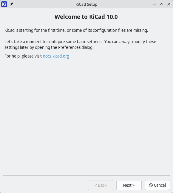
First time setup
The first time you open KiCad, a Welcome window appears to guide you through the initial setup.
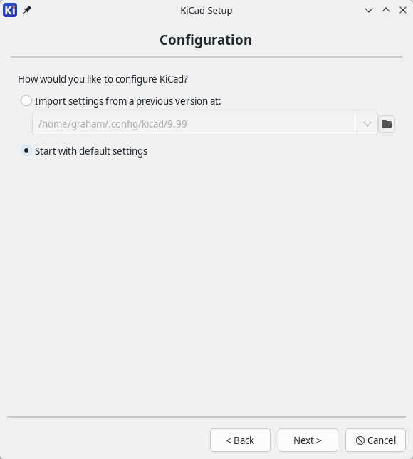
The next page asks you if you want to start with fresh preferences or if you want to import your settings from an older version of KiCad.
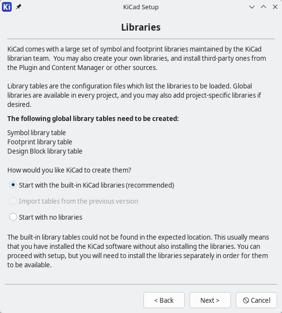
The next page asks you how you want to configure your symbol and footprint libraries. If you are setting up KiCad for the very first time, you should select the first option, Start with the built-in KiCad libraries. This initializes your library tables to include all of the libraries that come with KiCad.
If you have used an older version of KiCad and are updating it to the newest version, and therefore already have a library setup that worked in the old version, you can instead the select the second option, Import tables from the previous version. In this case, it is recommended to also select the option Migrate built-in libraries to the latest version, which replaces references to the old-version built-in libraries with references to the updated libraries.
You also have the option to start with no libraries and do all of the configuration yourself. Refer to the Schematic Editor and PCB Editor documentation for details on how to manually configure libraries.
Depending on your system and how KiCad was installed, some options may not be available. KiCad may also not be able to locate any libraries installed on your system. In this case, you should ensure you have installed the libraries, or you can manually configure the libraries after completing setup.
| On some systems the KiCad libraries are installed as a separate package. |
La posizione dei file tabella librerie predefinite dipende dal sistema operativo e può variare in base alla posizione di installazione. In basso le posizioni predefinite per ogni sistema operativo:
Windows |
|
Linux |
|
macOS |
|
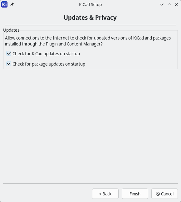
The last page asks you whether you want to automatically check for updates to the KiCad application and to third-party packages you may have installed through KiCad’s Plugin and Content Manager (plugins, themes, libraries, etc.).
On Windows, you also have the option to enable anonymous crash reporting, which helps the KiCad team diagnose and fix critical issues in the application.
Tutorial parte 1: il progetto
Opening KiCad will bring up the Project Manager. To create a new project:
-
Click File → New Project
-
Select the Default project template and click OK.
-
Browse to the location where you want to save your project, and give your project a name, such as
getting-started. -
Make sure the Create a new folder for the project checkbox is ticked.
-
Click Save.
This will create your project files in a new subfolder with the same name as your project.
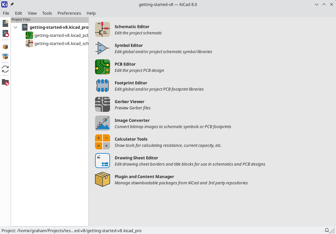
A sinistra, il riquadro File progetto elenca i file nel nuovo progetto. C’è un file progetto con estensione .kicad_pro, un file schema con estensione .kicad_sch e un file circuito stampato con estensione .kicad_pcb. Questi file condividono tutti lo stesso nome del progetto.
There may also be a -backups directory: KiCad can automatically create backups of your project when you save and when there are unsaved changes after several seconds of inactivity. The backup settings are configurable by going to Preferences → Preferences → Common → Project Backup.
| L’apertura della finestra delle preferenze può far aprire la configurazione della tabella delle librerie. Questa è descritta di seguito. |
| Su macOS, la finestra delle preferenze è nel menu KiCad, non nel menu delle Preferenze. |
A destra della finestra del progetto, ci sono dei pulsanti per avviare i vari strumenti forniti da KiCad. L’avvio di questi strumenti aprirà automaticamente il file di progettazione associato (dello schema o del C.S.) dal progetto corrente. Iniziare aprendo l’editor degli schemi elettrici.
Tutorial part 2: schematic
Schematic editor basics
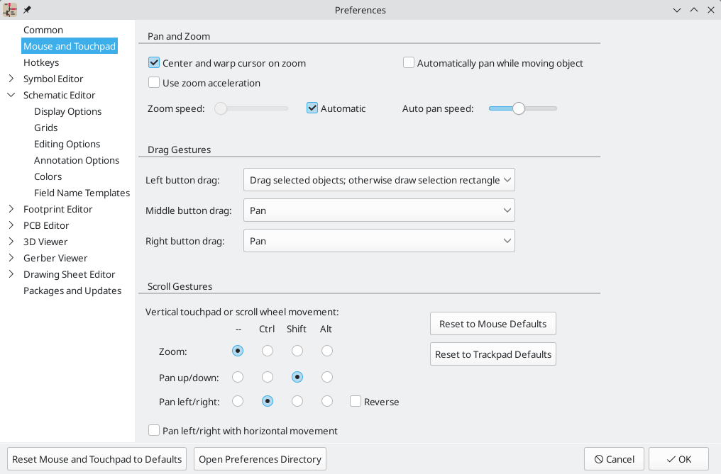
Per fare pan in giro per lo schema, fare clic e trascinare con il pulsante centrale o quello destro del mouse. Ingrandire e rimpicciolire con la rotellina or F1 e F2. Gli utenti dei portatili potrebbero trovare comodo cambiare i controlli del mouse per accordarli meglio con il touchpad; i controlli del mouse sono configurabili in Preferenze → Preferenze… → Mouse e Touchpad.
| Su macOS, la finestra delle preferenze è nel menu KiCad, non nel menu delle Preferenze. |
Per impostazione predefinita, KiCad abilita un’impostazione del mouse denominata Centra e sposta il puntatore con lo zoom. Quando questa funzione è abilitata, il cursore del mouse si sposta automaticamente al centro dello schermo quando l’utente esegue lo zoom avanti o indietro. Ciò mantiene la regione ingrandita sempre centrata. Questa funzione può sembrare un po' strana all’inizio, ma molti utenti la trovano utile una volta abituati. Provare a ingrandire e rimpicciolire con il puntatore del mouse in diverse aree dell’area di lavoro. Se il comportamento dello zoom predefinito risulta scomodo, disabilitare la funzione nelle preferenze Mouse e Touchpad.
La barra degli strumenti sul lato sinistro dell’editor degli schemi contiene le impostazioni di visualizzazione di base. La barra degli strumenti sul lato destro dello schermo contiene gli strumenti per modificare lo schema.
Some toolbar buttons have a small triangle in the bottom
right corner  . The triangle
indicates that the button has an expanding palette containing several
related tools, for example different kinds of labels. To select an
alternate tool, click and hold on the button until the palette appears,
then click on the alternate tool. Another way to use the palettes is to
click on the button and drag to the left until the palette appears, then
release the mouse button when the desired tool is highlighted. . The triangle
indicates that the button has an expanding palette containing several
related tools, for example different kinds of labels. To select an
alternate tool, click and hold on the button until the palette appears,
then click on the alternate tool. Another way to use the palettes is to
click on the button and drag to the left until the palette appears, then
release the mouse button when the desired tool is highlighted.
|
Alla maggior parte degli strumenti in KiCad sono assegnati comandi da tastiera predefiniti o possono essere assegnati comandi da tastiera personalizzati. Per visualizzare tutti i comandi da tastiera, andare su Aiuto → Elenco tasti…. I comandi da tastiera possono essere modificati nel pannello Comandi da tastiera della finestra delle Preferenze.
Schematic sheet setup
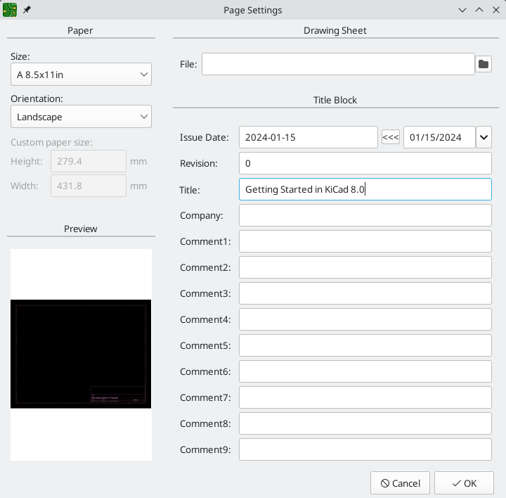
Prima di disegnare qualcosa nello schema, impostare il foglio dello schema stesso. Fare clic su File → Impostazioni pagina. Assegnare allo schema un titolo e una data e, se si vuole, modificare il formato della carta.
Adding symbols to the schematic
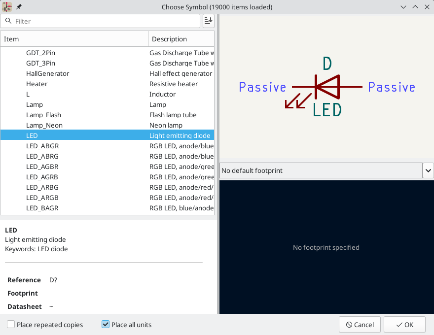
Iniziare a creare il circuito aggiungendo alcuni simboli allo schema. Aprire la finestra di dialogo Scegliere simbolo facendo clic sul pulsante Aggiungi simboli  sul lato destro della finestra o premendo A.
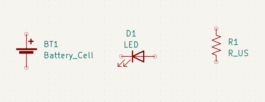
La finestra di dialogo Scegli simbolo elenca le librerie di simboli disponibili e i simboli dei componenti in esse contenuti. I dispositivi di base come componenti passivi, diodi e altri simboli generici si trovano nella libreria Device. Dispositivi specifici, come un tipo particolare di LED, si trovano nelle altre librerie.
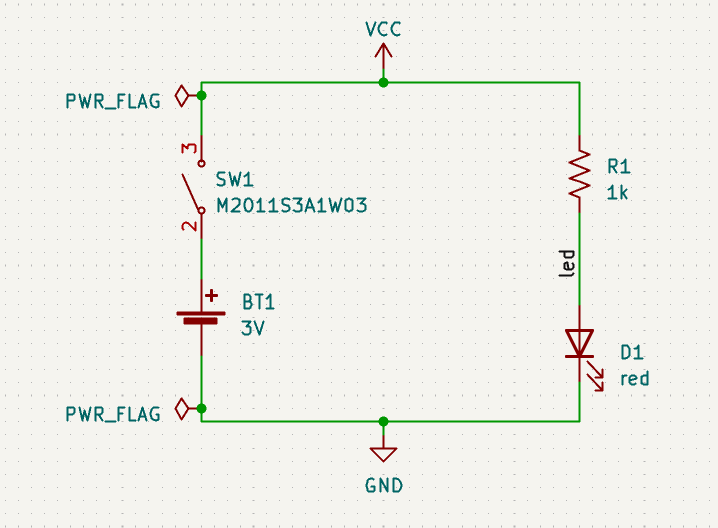
Scorrere verso il basso fino alla libreria "Device", espanderla e selezionare il simbolo "LED". Fare clic su OK e fare nuovamente clic per posizionare il simbolo nello schema.
Quindi, aggiungere una resistenza di limitazione di corrente. Tornare al selettore dei simboli, ma questa volta provare a cercare una resistenza inserendo "R" nella casella del filtro in alto. Di nuovo, si trova nella libreria Device. Il dispositivo R è un simbolo di resistenza rettangolare in stile IEC. Un simbolo R_US è disponibile anche per gli utenti che preferiscono il simbolo a zigzag in stile ANSI. Selezionare un simbolo di resistenza e aggiungerlo allo schema.
Infine, aggiungere una batteria per alimentare il LED. La libreria Device ha il simbolo appropriato Battery_Cell.
Selecting and moving objects
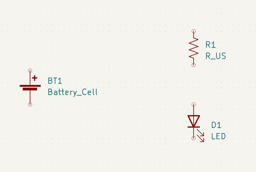
Poi, posizionare i simboli correttamente l’uno rispetto all’altro, come mostrato nello screenshot. A tale scopo, selezionare e poi spostare e ruotare i simboli.
In KiCad, gli oggetti vengono selezionati facendo clic sopra di essi mentre è attivo lo strumento di selezione. Lo strumento di selezione è lo strumento predefinito quando nessun altro strumento è attivo, quindi si può entrare nello strumento di selezione chiudendo qualsiasi strumento attivo (Esc) o facendo clic sul pulsante  nella barra degli strumenti di destra.
Ulteriori oggetti possono essere aggiunti alla selezione con Maiusc+clic, o rimossi con Ctrl+Maiusc+clic (MacOS: Cmd+Maiusc+clic).È possibile commutare lo stato della selezione di un oggetto con Ctrl+clic (macOS: Cmd+clic).
È anche possibile trascinare la selezione; trascinando da sinistra a destra si selezionano gli oggetti che sono interamente racchiusi dalla casella di selezione, mentre trascinando da destra a sinistra si selezionano anche gli oggetti che sono parzialmente racchiusi dalla casella di selezione. Maiusc, Ctrl+Maiusc (Cmd+Maiusc), e Ctrl (Cmd) possono essere utilizzati anche con la selezione trascinata, rispettivamente per aggiungere, sottrarre o commutare dalla selezione.
Si noti che è possibile selezionare un intero simbolo (facendo clic sulla forma del simbolo stesso) o selezionare un campo di testo nel simbolo senza selezionare il resto del simbolo (facendo clic sul testo). Quando viene selezionato solo un campo di testo, qualsiasi azione eseguita agirà solo sul testo selezionato e non sul resto del simbolo.
Gli oggetti selezionati vengono spostati premendo M e ruotati premendo R. Il tasto comando G (trascinamento) può essere utilizzato anche per spostare gli oggetti. Per lo spostamento di simboli non collegati, G e M si comportano in modo identico, ma per i simboli con fili collegati, G sposta il simbolo e mantiene i fili collegati, mentre M sposta il simbolo e lascia i fili indietro. Gli oggetti selezionati possono essere cancellati con il tasto Canc.
Wiring the schematic
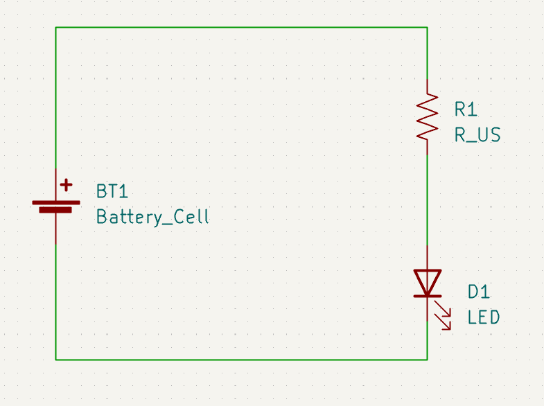
I pin dei simboli hanno tutti dei piccoli cerchi a indicare che non sono collegati. Risolvere disegnando fili tra i pin dei simboli come mostrato nella schermata. Fare clic sul pulsante Aggiungi un filo  sulla barra degli strumenti di destra o utilizzare il tasto comando W. Fare clic e rilasciare per iniziare a disegnare un filo e finire di disegnare il filo facendo clic sul pin di un simbolo o facendo doppio clic in un punto qualsiasi. Premendo Esc si annullerà il disegno del filo.
Un altro metodo conveniente per disegnare i fili è passare con il mouse su un pin scollegato. Il cursore del mouse cambierà per indicare che è possibile tracciare un filo a partire da quella posizione. Cliccando sul pin inizierà quindi a disegnare un filo automaticamente.
Quindi, aggiungere i simboli di potenza e terra allo schema. Sebbene non siano strettamente necessari in uno schema così semplice, facilitano la comprensione di schemi di grandi dimensioni.
Nella libreria dei simboli Power sono disponibili numerosi simboli di potenza / alimentazione e terra. Tuttavia, esiste una scorciatoia per aggiungere questi simboli: fare clic sul pulsante Aggiungi un simbolo di potenza  o usare il tasto comando P. Verrà visualizzata la finestra di dialogo Scegli un simbolo, ma verranno visualizzate solo le librerie di simboli che contengono i simboli di potenza e alimentazione.
Aggiungere un simbolo VCC e un simbolo GND e quindi collegarli al circuito con dei fili.
Finally, add a label to the wire between the LED and resistor. Again, this may not be necessary in a simple circuit, but it is good practice to label important nets. Click the Place Net Labels button  in the right toolbar (L), type a label name (
led), and place the label into the schematic so that the square attachment point overlaps with the wire. Rotate and align the label as necessary.
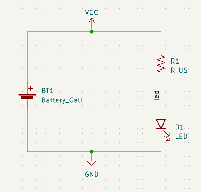
Si noti che le etichette e le porte di alimentazione con lo stesso nome vengono considerate collegate assieme. Un’altra porta di alimentazione GND o un cavo etichettato led in questo foglio di schema verrebbe cortocircuitato con quello esistente, anche senza fili che li collegano visivamente.
Annotation, symbol properties, and footprints
Annotazione
A ciascun simbolo occorre assegnare un riferimento univoco. Questo processo è noto anche come annotazione.
Per impostazione predefinita, i simboli vengono automaticamente annotati quando vengono aggiunti allo schema. L’annotazione automatica può essere abilitata o disabilitata utilizzando il pulsante  nella barra degli strumenti di sinistra.
Anche se non è necessario per questa guida, i simboli possono essere annotati o riannotati manualmente utilizzando il pulsante Compila i riferimenti dei simboli nello schema () nella barra degli strumenti in alto.
Symbol properties
Quindi, inserire i valori per ciascun componente. Selezionare il LED, fare clic con il pulsante destro del mouse e selezionare Proprietà… (E). Questo progetto utilizzerà un LED rosso, quindi cambiare il campo Valore in rosso. In un progetto reale, potrebbe essere meglio scrivere qui il numero di parte del produttore del LED. Si noti che è possibile modificare i riferimenti individualmente nelle proprietà di ciascun simbolo.
Questo progetto userà una batteria a bottone al litio da 3 V, quindi cambiare il campo Valore di BT1 in 3 `. Cambiare il valore della resistenza in `1k.
Footprint assignment
Infine, assegnare un’impronta a ciascun componente. Ciò definirà come ogni componente si collegherà al C.S.. Alcuni simboli vengono forniti con impronte preassegnate, ma per molti componenti ci sono più impronte possibili, quindi l’utente dovrà selezionare quella appropriata.
Esistono diversi modi per assegnare le impronte; un modo comodo è usare lo strumento di assegnazione impronte facendo clic sul pulsante ![]() nella barra degli strumenti in alto.
nella barra degli strumenti in alto.
Il riquadro sinistro di questa finestra elenca le librerie di impronte disponibili. Il riquadro centrale mostra i simboli nello schema. A tutti questi simboli verranno assegnate delle impronte. Il riquadro di destra mostra le impronte impostabili per il simbolo selezionato nel riquadro centrale. Per assegnare un’impronta a un simbolo, selezionare il simbolo nel riquadro centrale e fare doppio clic sull’impronta desiderata nel riquadro di destra. Si può ottenere un’anteprima dell’impronta facendo clic con il pulsante destro del mouse su un’impronta e selezionando Visualizza impronta selezionata.
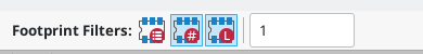
Molte impronte sono incluse in KiCad, quindi lo strumento di assegnazione delle impronte offre diversi modi per filtrare le impronte che non sono rilevanti per il simbolo in questione.
-
Il pulsante più a sinistra
 attiva i filtri che possono essere definiti in ogni simbolo. Ad esempio, un simbolo opamp potrebbe definire filtri che mostrano solo impronte SOIC e DIP. A volte quei filtri predefiniti mancano o sono troppo restrittivi, quindi può essere utile disattivare questo filtro in alcune situazioni.
 -
Il pulsante centrale
 filtra in base al conteggio dei pin, in modo che vengano mostrate solo le impronte di 8 pad per i simboli a 8 pin. Questo filtro è quasi sempre utile.
 -
Il pulsante destro
 filtra in base alla libreria selezionata. Le librerie sono selezionate nel riquadro di sinistra; le impronte non nella libreria selezionata verranno filtrate. Questo filtro è utile purché sia noto quale libreria contiene l’impronta corretta. Spesso è meglio usare questo filtro oppure i filtri simbolo, ma non entrambi.
 -
La casella di testo filtra le impronte che non corrispondono al testo nella casella. Questo filtro è disabilitato quando la casella è vuota.
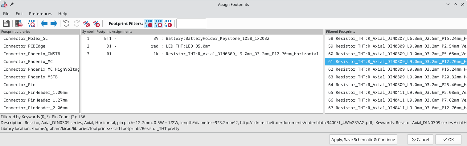
Usando i filtri, trovare ciascuna delle impronte mostrate nella colonna centrale della schermata qui sopra. Nella tabella sottostante sono elencate anche le impronte di ciascun simbolo. Assegnare ogni impronta a un simbolo selezionando il simbolo nella colonna centrale e quindi facendo doppio clic sull’impronta appropriata nella colonna di destra. Una volta assegnate tutte le impronte, fare clic su OK.
| Riferimento del simbolo | Impronte da assegnare |
|---|---|
|
|
|
|
|
|
Ci sono altri modi per assegnare le impronte; un modo è attraverso la finestra delle proprietà del simbolo. Per ulteriori informazioni sull’assegnazione delle impronte, consultare il manuale.
Electrical rules check
L’ultima cosa da fare nello schema è controllare gli errori di natura elettrica. Il controllo delle regole elettriche (ERC) di KiCad non può garantire che il progetto nello schema funzioni, ma può verificare che non sussistano banali problemi di connessione come pin scollegati, uscite di alimentazione in cortocircuito o ingressi di alimentazione non alimentati. Esso verifica anche la presenza di altri errori come simboli non annotati e errori di battitura nelle etichette delle connessioni. Per visualizzare l’elenco completo delle regole elettriche e regolarne l’importanza, andare su File→Impostazioni dello schema… → Regole elettriche → Importanza violazioni. È sempre una buona idea avviare un controllo regole elettriche prima di avviare la stesura del circuito stampato.
Eseguire un controllo delle regole elettriche facendo clic sul pulsante ERC  nella barra degli strumenti in alto e quindi facendo clic su Esegui ERC.
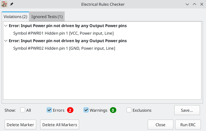
Anche in questo semplice schema, KiCad ha riscontrato due potenziali errori. Gli errori sono elencati nella finestra ERC e le frecce indicano le posizioni delle violazioni nello schema. Selezionando una violazione nella finestra ERC si evidenzia la freccia corrispondente.
Le violazioni si possono ignorare (per l’esecuzione ERC corrente) o escludere (da tutte le future esecuzioni ERC) facendo clic con il pulsante destro del mouse su ciascun messaggio di errore. Tuttavia, di solito vale la pena affrontare le violazioni, anche se non sono veri e propri errori di progettazione, al fine di ottenere un rapporto ERC pulito ed evitare di farsi sfuggire dei problemi reali.
In questo caso, KiCad segnala "Pin di potenza in ingresso non pilotato da alcun pin di potenza in uscita" per entrambe le reti VCC e GND. Questo è un classico errore ERC di KiCad. I simboli porta di potenza sono impostati per richiedere un pin di potenza di uscita, come l’uscita di un regolatore di tensione, sulla stessa rete; altrimenti KiCad potrebbe pensare che il collegamento non sia pilotato. Per un essere umano, è ovvio che VCC e GND sono pilotati dalla batteria, ma è necessario indicarlo esplicitamente nello schema.
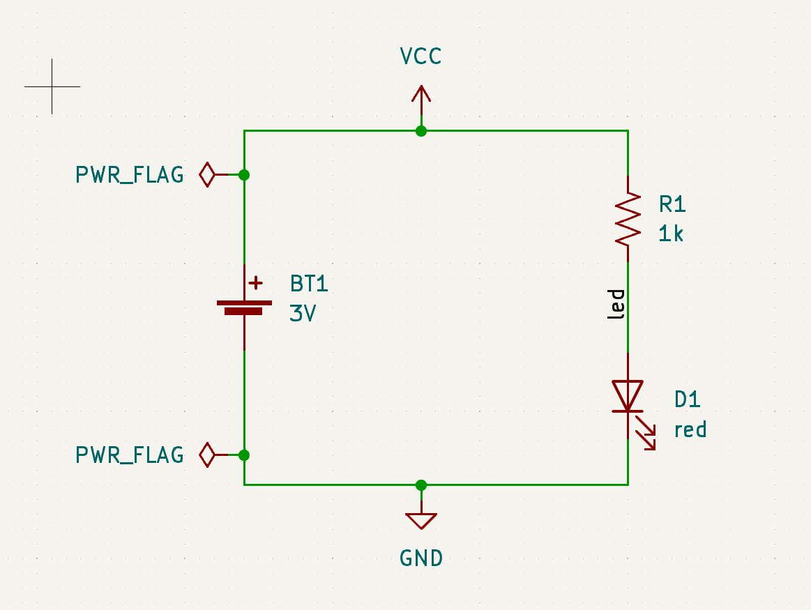
C’è uno speciale simbolo PWR_FLAG nella libreria dei simboli Power che viene usato per risolvere questo problema indicando a KiCad che i collegamenti sono effettivamente pilotati. Aggiungere questo simbolo alle net VCC e GND ed esegui nuovamente il controllo. Quando l’ERC passerà senza alcuna violazione, lo schema sarà completo.
Bill of materials
Un ultimo passaggio facoltativo consiste nel generare una distinta base che elenca tutti i componenti utilizzati nel progetto. Fare clic su Strumenti → Genera distinta materiali….
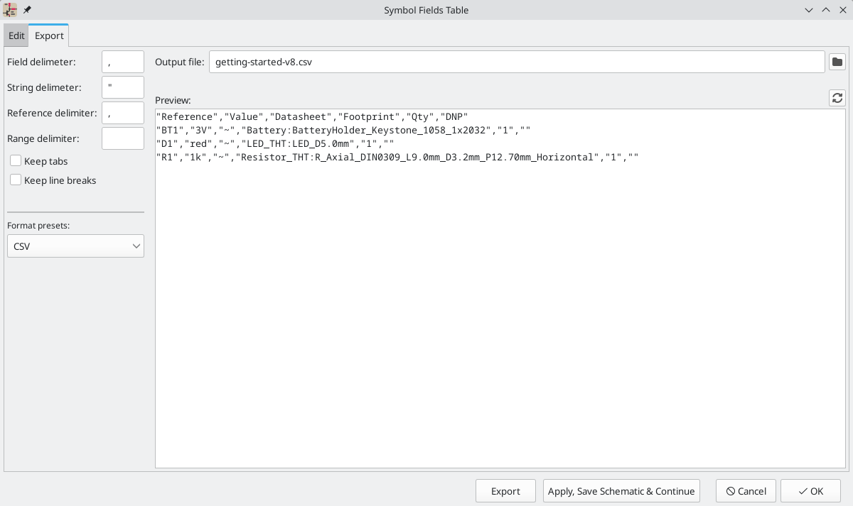
KiCad ha una GUI per l’esportazione della DIBA. È possibile configurare quali metadati dei simboli saranno esportati e come i simboli verranno raggruppati nella scheda Modifica e configurare il formato di uscita nella scheda Esporta.
Per ora, le impostazioni predefinite dovrebbero andare bene, ma è possibile osservare una vista grezza di ciò che verrà esportato nel riquadro di anteprima. Specificare un file di uscita nella scheda Esporta, e premere il pulsante Esporta.
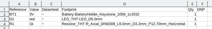
La DIBA dovrebbe assomigliare all’immagine di seguito se aperta in un programma di gestione dei fogli elettronici.
Tutorial part 3: circuit board
Con lo schema completato, tornare alla finestra del progetto e aprire l’editor del C.S. facendo clic sul pulsante Editor C.S. o aprendo il file dello stampato.
PCB editor basics
La navigazione nell’editor di circuiti stampati è la stessa dell’editor schemi elettrici: il pan si fa trascinando con il pulsante centrale del mouse o con il pulsante destro del mouse e per ingrandire invece con la rotellina del mouse o tramite F1/F2.
La parte principale dell’editor dei circuiti stampati. è la zona disegnabile al centro su cui viene steso il progetto della scheda. La barra degli strumenti sul lato sinistro ha varie opzioni di visualizzazione per la scheda, incluse le unità di misura e le modalità di visualizzazione bordo/pieno per tracce, via, pad e zone. La barra degli strumenti a destra dell’area di disegno contiene gli strumenti per la progettazione dello stampato.
|
Some toolbar buttons have a small triangle in the bottom
right corner . The triangle
indicates that the button has an expanding palette containing several
related tools, for example different kinds of dimensions. To select an
alternate tool, click and hold on the button until the palette appears,
then click on the alternate tool. Another way to use the palettes is to
click on the button and drag to the left until the palette appears, then
release the mouse button when the desired tool is highlighted.
|
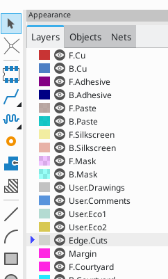
All’estrema destra c’è il pannello Aspetto e il filtro di selezione. Il pannello Aspetto viene utilizzato per modificare la visibilità, i colori e l’opacità di strati, oggetti e collegamenti dello stampato. Lo strato attivo viene modificato facendo clic sul nome dello strato.
Sotto il pannello Aspetto c’è il filtro di selezione, che abilita e disabilita la selezione di vari tipi di oggetti dello stampato. Ciò è utile per selezionare elementi specifici in un layout affollato.
Board setup and stackup
Prima di iniziare la progettazione dello stampato, impostare le dimensioni pagina e aggiungere informazioni al cartiglio. Fare clic su File → Impostazioni pagina…, quindi scegliere un formato carta appropriato e inserire data, revisione e titolo.
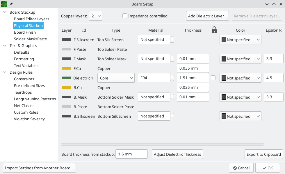
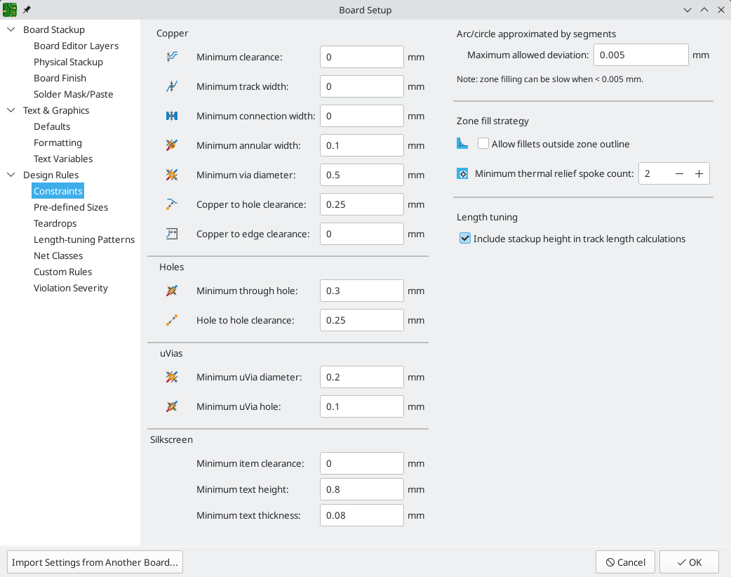
Quindi, andare su File → Impostazione scheda… per definire come verrà prodotto il circuito stampato. Le impostazioni più importanti sono lo stackup, ovvero quali strati di rame e dielettrico avrà il PCB (e i loro spessori) e le regole di progettazione, ad es. dimensioni e spaziatura per tracce e via.
Per impostare lo stackup, aprire la pagina Stackup scheda → Stackup fisico della finestra Impostazione scheda. Per questa guida, lasciare il numero di strati di rame a 2, ma progetti chiaramente più complessi potrebbero richiedere un numero maggiore di strati.
Successivamente, andare alla pagina Regole di progettazione → Vincoli. Le impostazioni in questa pagina specificano le regole di progettazione prioritarie per tutto il progetto della scheda. Ai fini di questa guida, le impostazioni predefinite vanno bene. Tuttavia, per un progetto reale, queste dovrebbero essere impostate in base alle capacità e caratteristiche del fabbricante di circuiti stampati in modo che il progetto del circuito stampato sia realizzabile.
Infine, aprire la pagina Regole di progettazione → Netclass. Una netclass è un insieme di regole di progettazione associate a un gruppo specifico di collegamenti. Questa pagina elenca le regole di progettazione per ciascuna netclass nel progetto e consente di associare specifici collegamenti a determinate netclass (i collegamenti possono anche essere assegnati alle netclass nell’editor dello schema).
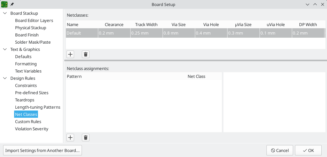
Larghezze e spaziature piste possono essere gestite manualmente dal progettista durante la stesura del C.S., ma l’uso delle netclass è consigliato perché forniscono un modo automatico per gestire e controllare le regole di progettazione.
In this design, no net classes are specified, so all nets will belong to the Default net class. A single net class is acceptable for this project, but other designs may have multiple net classes, each with different design rules. For example a board might have a High Current netclass with wide tracks, or a 50 ohm netclass with specific width and clearance rules for 50 ohm controlled-impedance tracks.
This project has relatively few components and is not space constrained, so we can be generous with track sizing. Larger tracks can carry more current and are more mechanically robust. Increase the Default net class’s Track Width from 0.2 mm to 0.4 mm. When we route tracks, they will automatically have a width of 0.4 mm.
Importing changes from schematic
Lo schema è completo, ma non ci sono ancora componenti nell layout. Per importare i dati di progettazione dallo schema nel C.S., fare clic su Strumenti → Aggiorna il C.S. dallo schema… o premere F8. C’è anche un pulsante  nella barra strumenti in alto.
Leggere i messaggi nella finestra Modifiche da applicare, che diranno che i tre componenti nello schema verranno aggiunti alla scheda. Fare clic su Aggiorna C.S., Chiudi e fare clic sull’area di disegno per posizionare le tre impronte. La posizione di ciascuna impronta rispetto alle altre verrà modificata in seguito.
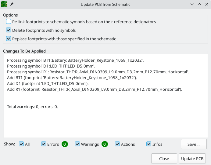
In KiCad, l’aggiornamento del C.S. con le modifiche allo schema è un processo manuale: il progettista decide quando è opportuno aggiornare il C.S. con le modifiche allo schema. Ogni volta che lo schema viene modificato, il progettista deve utilizzare lo strumento Aggiorna il C.S. dallo schema per mantenere lo schema e il layout sincronizzati.
Drawing a board outline
Ora i tre componenti sono stati posizionati, ma la scheda stessa non è stata definita. La scheda viene definita disegnando il bordo scheda sul livello Edge.Cuts.
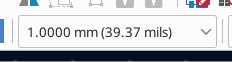
Spesso è utile disegnare il borso scheda con una griglia grossolana, rendendo facile ottenere numeri interi per le dimensioni della scheda. Passare a una griglia grossolana selezionando 1mm nel menu a discesa Griglia sopra la zona di lavoro.
Per disegnare sul livello Edge.Cuts, fare clic su Edge.Cuts nella scheda Strati del pannello Aspetto a destra. Scegliere lo strumento rettangolo  nella barra degli strumenti a destra e fare clic sull’area di disegno per piazzare il primo angolo e poi clic ancora per piazzare l’angolo opposto in modo da disegnare un rettangolo che circonda approssimativamente le tre impronte. Anche gli altri strumenti grafici (linea , arco
  , cerchio
  , poligono
  , bezier
  o una combinazione di questi) possono essere usati per disegnare il bordo della scheda; l’unico requisito è che sia un’unica forma chiusa che non intersechi sé stessa.
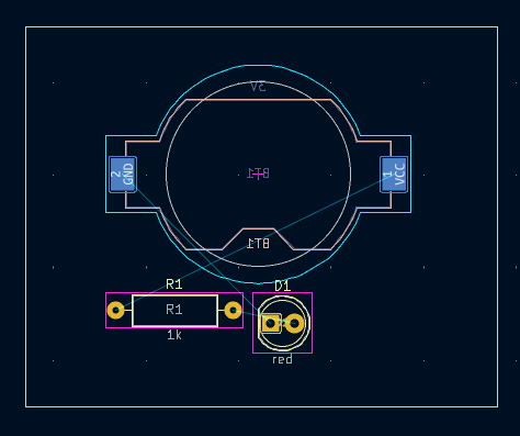
The board outline should look like this:
The lighter grey color inside the outline indicates the interior of the board.
Placing footprints
Il passaggio successivo nel processo di layout è disporre le impronte sulla scheda. In generale, ci sono diverse considerazioni per il posizionamento delle impronte:
-
Alcune impronte possono avere requisiti esatti per la loro posizione, come connettori, indicatori o pulsanti e interruttori.
-
Potrebbe essere necessario posizionare alcuni componenti in base a considerazioni elettriche. I condensatori filtro devono essere vicini ai pin di alimentazione dell’IC associato e i componenti analogici sensibili devono essere lontani da interferenze digitali.
-
Quasi tutti i componenti hanno un "ingombro" (N.d.T. 'courtyard') (o due se sono definiti sia il fronte che il retro). Generalmente gli ingombri non devono intersecarsi.
-
Otherwise components should be positioned for ease of routing. Connected components should generally be close together, and arranged to minimize routing complexity. The ratsnest (the thin lines indicating connections between pads) is useful for determining how best position footprints relative to other footprints.
Ai fini di questa guida, l’unico obiettivo del posizionamento è rendere il processo di sbroglio il più semplice possibile.
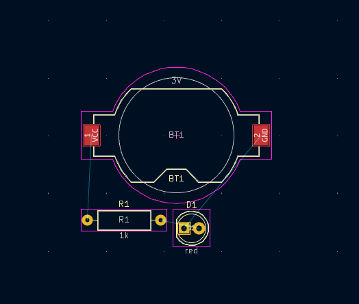
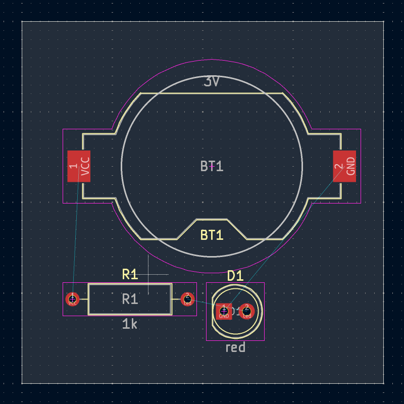
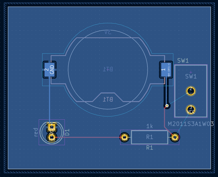
Start by moving the battery holder BT1 onto the back side of the board. Click it to select it, then press M to move it. Press F to flip it to the opposite side, then click to place it. It now appears mirrored and its pads have changed from red to blue.
Tutti gli strati del C.S. sono visualizzati dal lato anteriore della scheda. Le impronte sul fondo della scheda sono quindi capovolte e appaiono specchiate.
Ogni strato della scheda ha un colore univoco, mostrato dai campioni di colore nella scheda Livelli del pannello Aspetto. Nello schema colori predefinito, gli elementi sullo strato F.Cu (rame anteriore) sono rossi, mentre gli elementi sullo strato B.Cu (rame posteriore) sono blu.
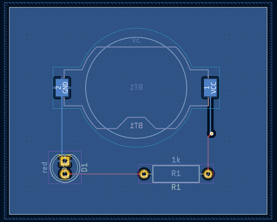
Now place the other two components. One at a time, select each component, then move and rotate it with M and R. The thin lines between pads are called ratsnest lines; they indicate connections in the schematic that you have not yet created in the PCB. Watch the ratsnest lines between each pad to choose the simplest arrangement of components; a good arrangement will leave the lines untangled, which means it will be easy to route the tracks between pads. One possible arrangement is shown in the screenshot below.
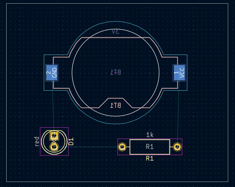
Routing tracks
Con i componenti a posto, è il momento di collegare le piazzole con le piste di rame.
La prima pista verrà disegnata sulla parte anteriore (fronte) della scheda, quindi cambiare lo strato attivo in "F.Cu" nella scheda strati del pannello Aspetto.
Fare clic su Sbroglia tracce  nella barra degli strumenti a destra o premere X. Fare clic sulla piazzola "led" di "D1". La ratsnest indica che c’è una connessione non instradata alla piazzola "led" di "R1", quindi fare clic su quella piazzola per tracciare una pista che collega le due piazzole. Cliccando sulla seconda piazzola si completa la pista. La linea Ratsnest tra i piedini
 led non è più disegnata perché la connessione è stata realizzata in rame.
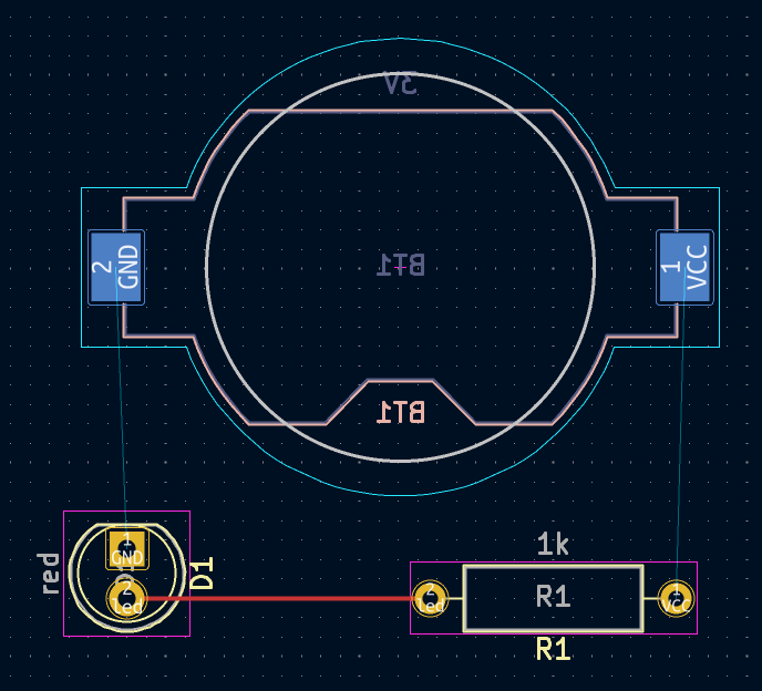
Ora tracciare una pista tra le piazziole GND di BT1 e D1, iniziando dalla piazzola BT1 sul retro della scheda. Notare che il livello attivo è cambiato automaticamente in B.Cu dopo aver fatto clic sulla piazzola BT1. Fare clic sulla piazzola D1 per terminare la pista.
Mentre BT1 ha piazzole a montaggio superficiale che si trovano solo nella parte inferiore della scheda, D1 ha piazzole con foro passante che possono collegarsi alle piste sia sulla parte anteriore che su quella posteriore. Le piazzole passanti sono un modo per creare una connessione tra più strati. In questo caso, D1 è un componente sul lato anteriore della scheda, ma i suoi fori passanti vengono utilizzati per connettersi a una pista sul retro della scheda.
Un altro modo per stabilire una connessione tra strati è tramite un via. Iniziare lo sbroglio dalla piazzola VC di BT1 sul retro della scheda. Premere V e fare clic a metà strada tra BT e R1 per inserire un via, operazione che commuta anche lo strato attivo su F.C. Completare la pista sul lato superiore della scheda facendo clic sulla piazzola VCC di R1.
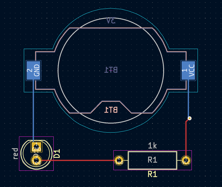
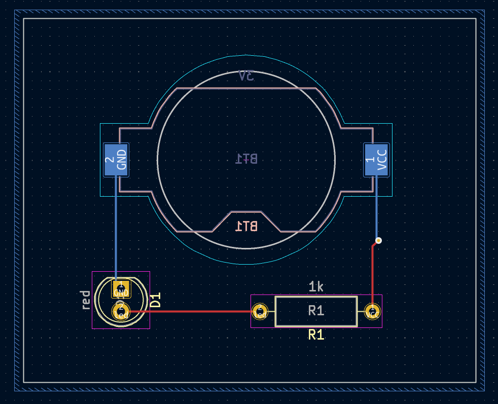
A questo punto, tutte le connessioni (net) sono sbrogliate. Ciò può essere confermato guardando la schermata di stato in basso a sinistra della finestra, dove il numero di connessioni non sbrogliate è indicato come 0.
Placing copper zones
Le zone di rame sono regioni di rame con un collegamento (net) associato. Le zone si collegano automaticamente agli oggetti di rame che appartengono allo stesso collegamento ed evitano gli oggetti che appartengono ad altri collegamenti. Le zone sono spesso utilizzate per connessioni di terra e di alimentazione perché forniscono una connessione a impedenza inferiore rispetto alle piste.
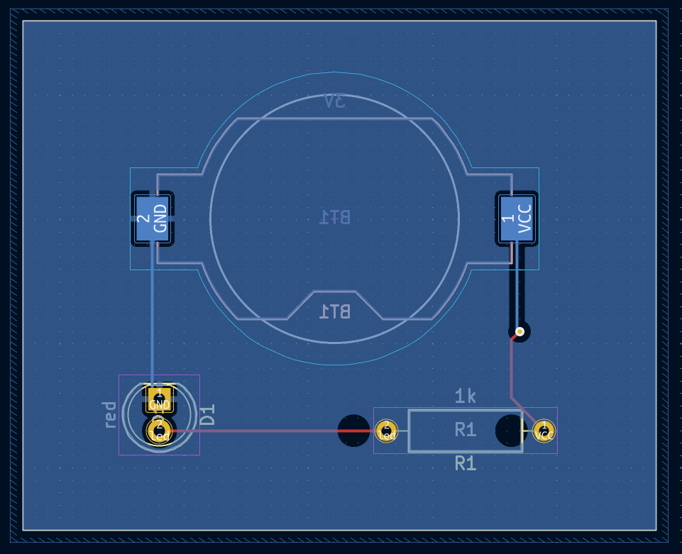
Aggiungere una zona GND sul retro scheda passando allo strato di rame inferiore e facendo clic sul pulsante Aggiungi una zona piena  nella barra degli strumenti di destra. Fare clic sul C.S per posizionare il primo vertice della zona.
In the Copper Zone Properties dialog that appears, select the GND net from the Net name dropdown and make sure that the B.Cu layer is selected. Click OK, then click to place the other three corners of the zone. Double click when placing the last corner to complete the zone.
Il contorno zona viene visualizzato sull’area di disegno, ma la zona non è ancora riempita: non c’è rame nell’area della zona e pertanto la zona non effettua alcun collegamento elettrico. Riempire la zona con Modifica → Riempi tutte le zone (B). Il rame è stato aggiunto alla zona, ma non si collega alle piazzole e alle piste VCC o led ed è tagliato dal bordo della scheda. Si sovrappone alla pista GND disegnata in precedenza e si collega alla piazzola GND tramite piste sottili. Si tratta di supporti termici che facilitano la saldatura della piazzola. I supporti termici e altre impostazioni della zona possono essere modificati nella finestra di dialogo delle proprietà della zona.
In KiCad, le zone non vengono riempite automaticamente quando vengono disegnate o modificate per la prima volta, o quando le impronte al loro interno vengono spostate. Le zone vengono riempite riempiendole manualmente e quando si eseguono i controlli regole elettriche. Assicurarsi che i riempimenti delle zone siano aggiornati prima di generare file di fabbricazione.
A volte le zone riempite possono rendere difficile vedere altri oggetti in una scheda affollata. Le zone possono venire nascoste a parte i confini tramite il pulsante Mostra solo i confini delle zone  sulla barra degli strumenti a sinistra. Le zone mantengono il loro stato riempito quando vengono mostrati solo i contorni: nascondere il riempimento di una zona non equivale a svuotarla.
Le zone possono anche essere rese trasparenti utilizzando il pannello Aspetto e i livelli inattivi possono anch’essi essere nascosti o oscurati utilizzando le Opzioni di visualizzazione dei livelli nel pannello Aspetto.
Design rule checking
Il controllo delle regole di progettazione (DRC) è l’equivalente del controllo delle regole elettriche del circuito stampato ma per lo schema elettrico. Il DRC cerca errori di progettazione come discrepanze tra lo schema e la scheda, regioni di rame che hanno una distanza insufficiente o sono in cortocircuito e tracce che non si collegano a nulla. Si possono scrivere anche regole personalizzate. Per visualizzare l’elenco completo delle regole di progettazione che vengono controllate e per regolarne l’importanza, andare su File → Impostazione scheda… → Regole di progettazione → Importanza violazioni. Si consiglia di eseguire il DRC e correggere tutti gli errori prima di generare alcun file di fabbricazione.
Eseguire un controllo DRC con Ispeziona → Verifica regole di progettazione o utilizzare il pulsante nella barra degli strumenti in alto. Fare clic su Esegui DRC. Una volta completati i controlli, non dovrebbero essere segnalati errori o avvisi. Chiudere la finestra DRC.
Ora causare intenzionalmente un errore DRC spostando l’impronta della resistenza in modo che si sovrapponga all’area riempita della zona. Utilizzare D (Trascina) per spostare leggermente l’impronta della resistenza mantenendo le tracce attaccate alle sue piazzole. Ciò crea una violazione della distanza perché le piazzole VCC e led del resistore sono in cortocircuito dal riempimento della zona GND. Normalmente questo problema verrebbe risolto riempiendo nuovamente la zona, ma non riempire ancora la zona.
Eseguire nuovamente il DRC, ma assicurarsi di deselezionare la casella di controllo Aggiorna tutte le zone prima di eseguire il DRC. Il DRC segnala 6 violazioni: per ciascuna piazzola di R1, c’è una violazione di spazio tra la piazzola e la zona, un’altra violazione di spazio tra il foro passante della piazzola e la zona e una terza violazione dove l’apertura della maschera di saldatura espone il rame di due diverse connessioni (lo riempimento GND e la pista connessa alla piazzola). Le frecce indicano ciascuna violazione nell’area di disegno. Facendo clic su ciascun messaggio di violazione si ingrandisce la visualizzazione sulla rispettiva violazione.
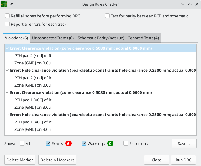
Chiudere la finestra di dialogo DRC, premere B per riempire la zona e rieseguire il DRC. In alternativa, selezionare la casella di controllo Riempire tutte le zone prima di eseguire il DRC ed eseguire nuovamente il DRC. Tutte le violazioni sono state corrette.
3D viewer
KiCad offre un visualizzatore 3D utile per ispezionare il C.S. . Aprire il visualizzatore 3D con Visualizza → Visualizzatore 3D. Effettuare la panoramica trascinando con il pulsante centrale del mouse e orbitare trascinando con il pulsante sinistro del mouse. Orbitare attorno al circuito stampato per vedere il LED e il resistore in alto e il supporto della batteria in basso.
È disponibile una modalità raytracing, che è più lenta ma offre un rendering più accurato. Passare alla modalità raytracing con Preferenze → Raytracing.
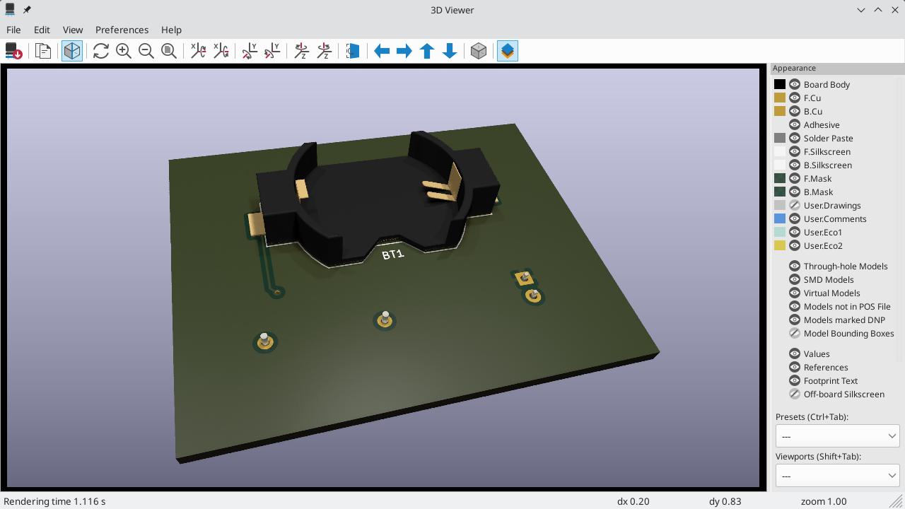
Molte delle impronte nella libreria di KiCad sono dotate di modelli 3D, incluse tutte le impronte utilizzate in questa guida. Alcune impronte non vengono fornite con modelli 3D, ma gli utenti possono aggiungerne di propri.
Fabrication outputs
Una volta completata la progettazione della scheda, il passaggio finale consiste nel generare i file necessari per la fabbricazione in modo che la scheda possa essere prodotta.
Aprire la finestra di dialogo Traccia, tramite File → Traccia…. Questa finestra di dialogo può tracciare il progetto in diversi formati, ma Gerber è solitamente il formato giusto per l’ordine di un C.S. da un produttore.
Specify an output directory so that the plotted files will be collected in a folder. Otherwise, the default settings are fine, but make sure all the necessary layers are checked:
-
Copper layers (
*.Cu). -
Board outline (
Edge.Cuts). -
Solder mask (
*.Mask). -
Silkscreen (
*.Silkscreen). -
Solder paste (
*.Paste). This layer is needed for manufacturing solder paste stencils, but is otherwise optional.
Other layers may be useful to plot, but are not typically necessary for PCB fabrication.
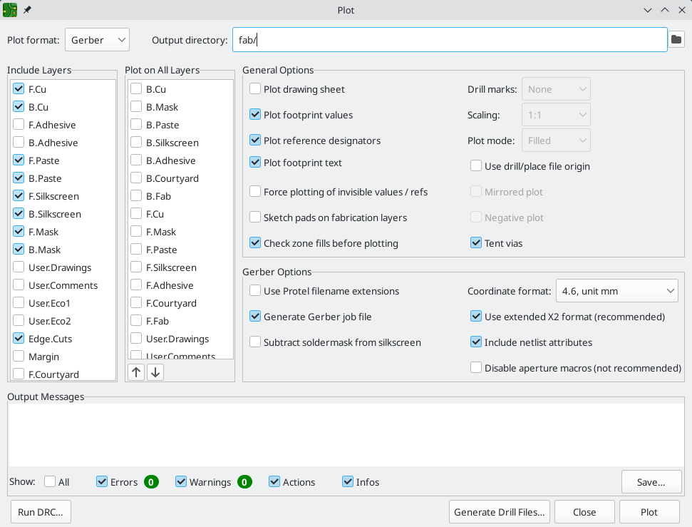
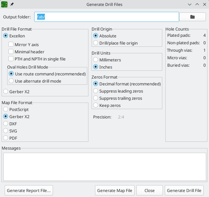
Fare clic su Traccia per generare i file Gerber. Fare inoltre clic su Genera file forature… e quindi su Genera file forature per creare file specificando la posizione di tutti i fori che verranno praticati nella scheda. Infine, chiuderela finestra di dialogo Traccia. Il progetto è finito.
Tutorial part 4: custom symbols and footprints
Il circuito può essere migliorato aggiungendo un interruttore per accendere e spegnere il LED. Il processo per aggiungere questo interruttore richiederà la creazione di una nuova libreria di simboli e impronte, il disegno di un simbolo di interruttore e la creazione di un’impronta per l’interruttore.
L’interruttore specifico che verrà utilizzato in questa guida è NKK M2011S3A1W03, un interruttore a levetta SPST. Potrebbero essere utilizzati molti altri interruttori, ma potrebbe essere necessario modificare la numerazione dei pin e l’ampiezza dell’ingombro.
Library and library table basics
Symbols and footprints are organized into libraries. A library can hold symbols or footprints, but not both.
KiCad keeps track of the user’s symbol libraries and footprint libraries in the symbol library table and footprint library table, respectively. Each library table is a list of library names and the location of where each library exists on disk. Library tables can also include other library tables, which effectively adds all of the libraries in the child table to the parent table.
In addition to global symbol and footprint library tables, there are also project library tables for symbols and footprints. Symbols and footprints that are added to the global tables are available in all projects, while symbols and footprints in the project-specific tables are available only for that specific project. Users can add their own libraries to the global library tables or to project-specific tables.
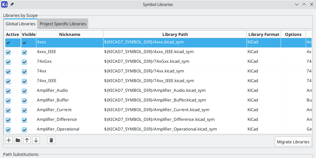
Le tabelle delle librerie di simboli possono essere visualizzate o modificate con Preferenze → Gestisci librerie di simboli… nelle finestre dell’Editor degli schemi elettrici o dell’Editor dei simboli. Le tabelle delle librerie di impronte possono essere visualizzate o modificate con Preferenze → Gestisci librerie di impronte… nell’editor dei circuiti stampati o nell’editor delle impronte. È possibile accedere a entrambe le tabelle di librerie anche dalla finestra di gestione del progetto.
Spesso i percorsi delle librerie sono definiti con variabili di sostituzione del percorso. Ciò consente a un utente di spostare tutte le proprie librerie in una nuova posizione senza modificare le tabelle delle librerie. L’unica cosa che deve essere cambiata è la definizione della variabile in modo che punti alla nuova posizione. Le variabili di sostituzione del percorso di KiCad vengono modificate con Preferenze → Configura percorsi… nella Gestione del progetto o in qualsiasi finestra di editing.
Una utile variabile di sostituzione del percorso è ${KIPRJMOD}. Questa variabile punta sempre alla cartella del progetto corrente, quindi può essere utilizzata per includere librerie specifiche del progetto archiviate nella cartella del progetto.
On first run, KiCad prompts the user to set up the symbol and footprint library tables. To reset your libraries to default, press the Reset Libraries button in the library table dialog.
Creating new global or project libraries
Il primo passo per disegnare un nuovo simbolo o impronta è scegliere una libreria nella quale memorizzarlo. Per questa guida, il simbolo e l’impronta dell’interruttore verranno inseriti nelle nuove librerie specifiche del progetto.
-
Open the Symbol Editor from the Project Manager.
-
Click File → New Library.
-
Select the Add new library to project library table option in the file browser.
-
Choose a name for the new library (e.g.
getting-started.kicad_sym). -
Save the new symbol library in the project directory.
The empty new library is now selected in the Libraries pane at left, and has been automatically added to the project library table (check the Project Specific Libraries tab in Preferences → Manage Symbol Libraries…).
Creating new symbols
Now create the switch symbol in the new library.
-
Select the
getting-startedlibrary in the Libraries pane at left. -
Click File → New Symbol….
-
In the Symbol name field, enter the part number:
M2011S3A1W03. -
Switch symbols should have reference designators that start with
SW, so change the Default reference designator field toSW. -
Uncheck Show pin name text.
-
Leave all other fields as the defaults.
-
Press OK.
Nel pannello Librerie, il simbolo M2011S3A1W03 ora appare sotto la libreria getting-started. Nell’area di disegno, una croce indica il centro dell’impronta ed è stato aggiunto del testo per il riferimento. Per ora, spostare il testo lontano dal centro dell’impronta per toglierlo di mezzo.
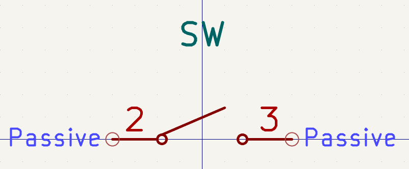
Symbol pins
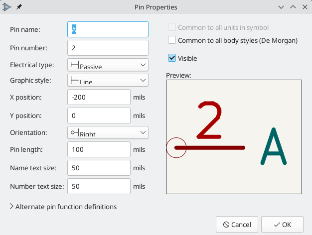
Iniziare a disegnare il simbolo aggiungendo un pin. Questo simbolo non avrà un pin 1, quindi si inizierà con un pin numero 2. Fare clic sul pulsante Aggiungi pin  sulla barra degli strumenti a destra. Apparirà la finestra di dialogo Proprietà pin. Impostare le proprietà del pin come segue:
-
Pin name:
A -
Pin number:
2 -
Electrical type:
Passive -
Orientation:
Right -
X Position:
-200 mils -
Y Position:
0
Fare clic su OK e poi sull’area di disegno per posizionare il piedino. Se il pin si è spostato dopo aver fatto clic su OK, potrebbe essere necessario modificare nuovamente le proprietà del piedino (fare doppio clic sul piedino o fare clic con il pulsante destro del mouse sul piedino → Proprietà…) per impostare la posizione corretta.
| Si consiglia vivamente di utilizzare sempre mil (o pollici) nell’editor degli schemi e in quello dei simboli, in particolare per i pin dei simboli. Mescolare unità imperiali e metriche darà luogo a pin dei simboli impossibili da collegare correttamente perché non allineati con fili o altri pin. Le librerie KiCad usano una griglia da 50 mil per i loro pin; l’utilizzo di un sistema di unità diverso impedirà ai simboli e agli schemi di connettersi con i simboli incorporati di KiCad. Si noti che, a differenza dell’editor di C.S., le unità nello schema non hanno alcun significato fisico. |
Aggiungere un secondo piedino, ma questa volta senza lo strumento Aggiungi piedino. Invece, premere Ins. Un nuovo pin numero 3 viene aggiunto al simbolo, appena sotto il piedino 2.
| In molti posti in KiCad, la pressione di Ins ripeterà l’ultima azione. La posizione del nuovo elemento verrà spostata e la numerazione incrementata automaticamente, se possibile. Nell’editor del simbolo, ciò può essere usato per piazzare velocemente molti piedini. Nell’editor degli schemi, può essere usato per piazzare ripetutamente un componente, o per etichettare i piedini di un grosso componente con etichette numerate. Ins può essere utile, infine, anche nell’editor delle impronte e del circuito stampato. |
Vogliamo che il Pin 3 si trovi a destra del simbolo dell’interruttore, quindi ne modificheremo le proprietà per cambiarne la posizione e l’orientamento. Invece di utilizzare la finestra di dialogo Proprietà Pin, questa volta possiamo utilizzare il Pannello Proprietà. Si tratta di un pannello ancorato sul lato sinistro dell’area di modifica che consente di visualizzare e modificare le proprietà dell’oggetto o degli oggetti selezionati. Per visualizzare o nascondere il Pannello Proprietà, utilizzare il pulsante  nella barra degli strumenti a sinistra.
Con il pin 3 selezionato, utilizzare il pannello Proprietà per impostarne le proprietà come segue:
-
Pin Name:
B -
Position X:
200 mils -
Position Y:
0 -
Orientation:
Left
| Il pannello Proprietà è disponibile in tutti gli editor KiCad (Schema, Scheda, Simbolo e Impronta). |
Symbol graphics
Con i piedini piazzati, usare gli strumenti cerchio e linea per far assomigliare il simbolo ad un interruttore SPST. Per realizzare questo passo, può essere utile impostare la griglia ad un valore più fine: clic destro sull’area di disegno e selezionare una griglia più piccola nel sottomenu Griglia. Dopo aver aggiunto le forme grafiche, impostare nuovamente la griglia a 50 mils.
| Le griglie fini sono utili per le grafiche, ma i piedini del simbolo devono essere sempre piazzati su una griglia di 50 mils (1.27 mm). I piedini non allineati alla griglia da 50 mils non si connetteranno ai fili nello schema. |
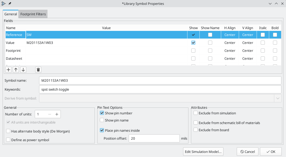
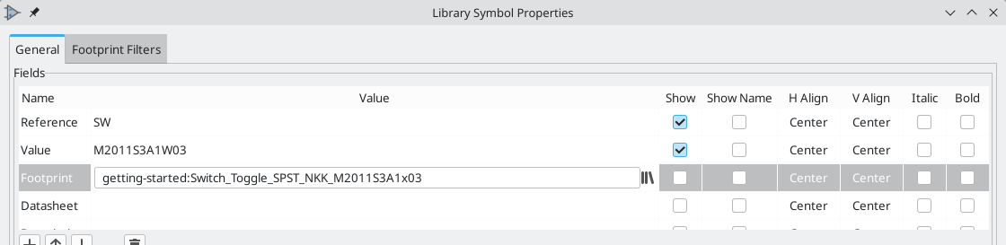
Symbol properties
Now edit the properties for the whole symbol with File → Symbol Properties, or by double clicking on the canvas. Change the Value field to M2011S3A1W03, and add spst switch toggle to the Keyword field to make it easier to find the symbol by searching.
Dopo aver fatto clic su OK, spostare il testo del campo valore più in basso in modo che non si sovrapponga alla grafica del simbolo.
Il simbolo ora è completo. Salvarlo e proseguire con la creazione di un’impronta.
Creating new footprints
To create a new footprint, follow a similar process as for symbols. First you need to create a library, then create a new footprint in the library.
-
Open the Footprint Editor from the Project Manager.
-
Click File → New Library….
-
Select the Add new library to project library table option in the file browser.
-
Choose a name for the new library (e.g.
getting-started.pretty) -
Save the new footprint library in the project directory.
As with the symbol library, the new footprint library is added to the project library table. You can now add a footprint to the new library.
-
Select the
getting-startedlibrary in the Libraries pane at left. -
Click File → New Footprint. This creates an empty, untitled footprint.
-
Edit the footprint’s properties (
 button in the top toolbar) and set the following properties:
-
Footprint name:
Switch_Toggle_SPST_NKK_M2011S3A1x03 -
Value:
Switch_Toggle_SPST_NKK_M2011S3A1x03 -
Component type: Through hole
-
Footprint pads
L’interruttore ha due piedini, numerati nella scheda tecnica come 2 e 3 e distanziati di 4,7 mm l’uno dall’altro. Per facilitare il posizionamento, regolare la griglia in modo che corrisponda alla spaziatura delle piazzole. Aprire le proprietà della griglia facendo clic destro sul pulsante  nella barra a sinistra e selezionare *Modifica griglia…. Aggiungere una nuova griglia con il pulsante del segno più, in basso. Impostare la nuova dimensione X della griglia a
 4.7 mm. Accettare la modifica nella finestra di dialogo, quindi tornare all’area di lavoro e passare alla nuova griglia nell’elenco a discesa della barra superiore se non è già selezionata.
By convention, through-hole footprints have pin 1 located at (0,0) and are oriented with pin 1 in the top left. We are using the SPST version of this switch which does not have pin 1, so the footprint will leave (0,0) empty and place pads 2 and 3 at (0, 4.7 mm) and (0, 9.4 mm). Note that in KiCad’s default coordinate system, the positive Y-axis is oriented downwards.
| Le coordinate X e Y del puntatore vengono visualizzate nella barra di stato nella parte inferiore della finestra. Si può usare questa informazione per controllare le coordinate quando si disegna o posiziona qualcosa. |
-
Use the Add a pad tool
 in the right toolbar to place a pad one grid division below the origin, which is (0, 4.7 mm).
 -
Press Esc to exit the pad tool.
-
Double click on the pad to edit its properties.
-
Change the pad number to
2. -
Verify that the position is correct.
-
Set the pad shape to Circular.
-
Set the hole diameter. The switch pins are 1.17 mm x 0.8 mm, which gives a diagonal (maximum pin dimension) of 1.42 mm. Therefore set the hole diameter to 1.42 mm + 0.2 mm =
1.62 mm. -
Set the pad diameter. For a hole diameter of 1.62 mm, set the pad diameter to 1.62 mm + 2*0.15 mm =
1.92 mmto provide a sufficient annular ring. -
Press OK to apply the pad modifications.
Ora usare nuovamente lo strumento Aggiungi piazzola per posizionare l’altra piazzola a (0,0 , 9.4 mm). Si noti che il numero della piazzola viene incrementato automaticamente e le proprietà, tra cui la dimensione della piazzola e la dimensione del foro, vengono copiate dalla piazzola precedente.
Con entrambi i cuscinetti posizionati, gli anulari appaiono leggermente piccoli. L’interruttore sarà più facile da saldare e meccanicamente più robusto se gli anelli anulari saranno più grandi. Aumentare lo spessore dell’anulare da 0,15 mm a 0,3 mm modificando la piazzola 2 e cambiando la dimensione del piazzola a 1,62 mm + 2*0,3 mm = 2,22 mm. Non modificare la dimensione del foro. Tenere presente che il campo della dimensione della piazzola accetta espressioni matematiche, quindi è possibile inserire direttamente "1,62+2*0,3" e verrà valutato 2,22 mm.
| Molte caselle di testo in KiCad supportano espressioni matematiche, inclusa l’unità conversioni. |
Apportare la stessa modifica all’anulare anche all’altra piazzola. Come scorciatoia, fare clic con il pulsante destro del mouse sulla piazzola 2, fare clic su Invia proprietà piazzola ad altre piazzole…, quindi fare clic su Cambia piazzole nell’impronta corrente.
Footprint graphics
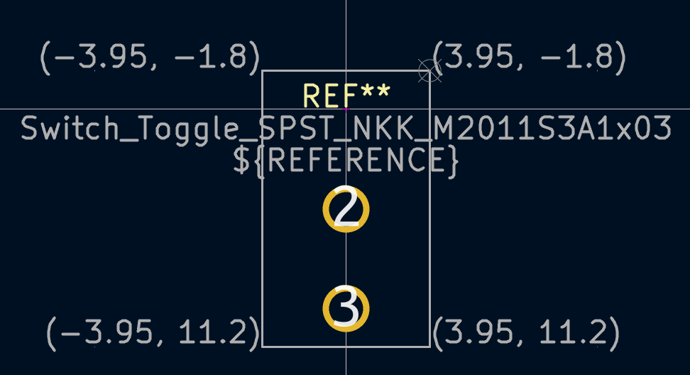
Una buona impronta avrà il contorno del componente disegnato esattamente sullo strato di fabbricazione (F.Fab), un contorno leggermente più grande sullo strato serigrafico (F.Silkscreen) e un ingombro (F.Courtyard) che circonda l’intera impronta per evitare sovrapposizioni con altre impronte.
The fabrication outline should precisely match the physical dimensions of the part, which is 7.9 mm wide and 13 mm tall. One way to precisely place the outline is to create a new grid with the correct X and Y spacing, as we did for the pads. Make sure to uncheck the Linked checkbox in the Grid Settings dialog to allow unequal X and Y grid spacing. You can then adjust the grid origin by right clicking the button and selecting Grid Origin….
Configurare l’origine e la spaziatura griglia come di seguito:
-
X griglia:
7.9 mm -
Y griglia:
13 mm -
Origine X: 7,9 mm / 2 =
3,95 mm -
Origine Y: 4,7 mm - (13 mm / 2) =
-1,8 mm.
To draw the fab outline, switch to the front fabrication layer by clicking F.Fab in the Layers panel at right. Use the line , rectangle , or polygon tools to draw the outline of the part as shown in the screenshot below, with corner coordinates annotated.
If you use the rectangle tool, you will need to make sure the line mode is set to the free-angle mode or you will only be able to draw squares.
To change the line mode to free-angle, click the  / /  / /  button on the left toolbar until it shows .
You can also use Shift+Space to cycle the line mode. button on the left toolbar until it shows .
You can also use Shift+Space to cycle the line mode.
|
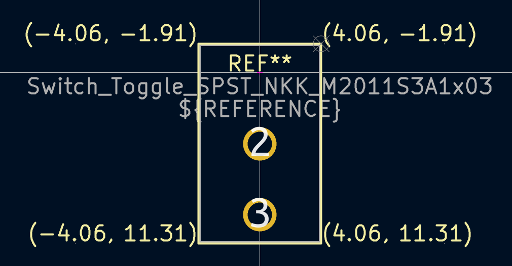
Successivamente, passare allo strato F.Silkscreen. Vogliamo che il contorno della serigrafia si trovi appena all’esterno del contorno del componente, in modo che le linee della serigrafia vengano spostate verso l’esterno dal disegno di fabbricazione di 0,11 mm (metà della larghezza della linea di fabbricazione di 0,10 mm, più metà della larghezza della linea della serigrafia di 0,12 mm). Le coordinate esatte sono mostrate nella schermata qui sotto e le impostazioni utili della griglia sono:
-
Griglia X: 7,9 mm + 2 * 0,11 mm =
8,12 mm -
Griglia Y: 13 mm + 2 * 0,11 mm =
13,22 mm -
Origine X: 8,12 mm / 2 =
4,06 mm -
Origine Y: -1,8 mm - 0,11 mm =
-1,91 mm
Also change the silk outline thickness to 0.12 mm by selecting each outline segment and editing its properties (right click → Properties… or press E).
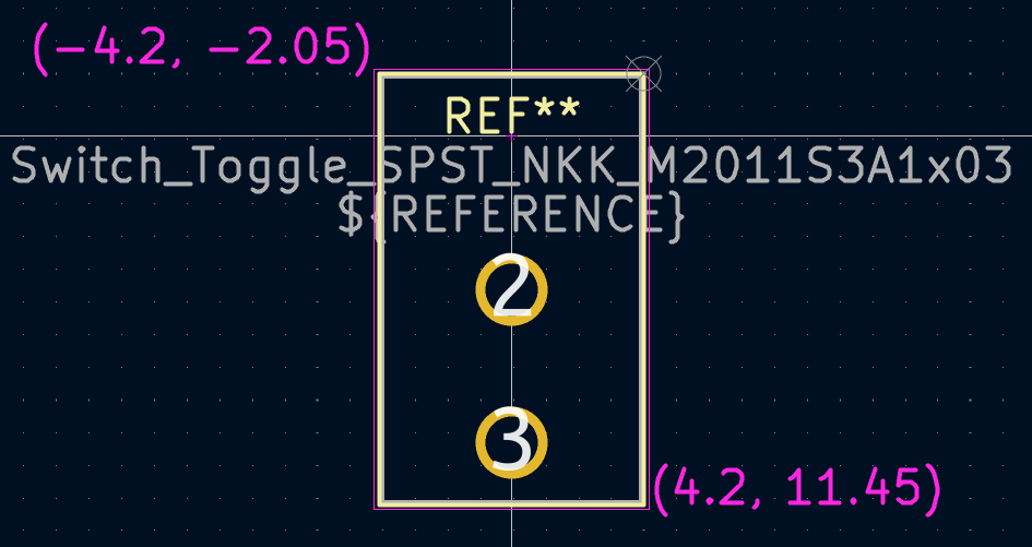
Infine, selezionare lo strato F.Courtyard. Vogliamo che il contorno dell’ingombro circondi il componente ad una distanza di 0,25 mm.
Per cambiare, usare una strategia diversa per disegnare questo strato. Passare a una griglia da 1mm invece di usare una griglia personalizzata e disegnare un rettangolo che circonda approssimativamente l’impronta. Selezionare il rettangolo e premere E per modificarne le proprietà e inserire direttamente le coordinate dell’angolo del rettangolo. Queste sono:
-
In alto a sinistra:
(-4.2, -2.05) -
In basso a destra:
(4.2, 11.45)
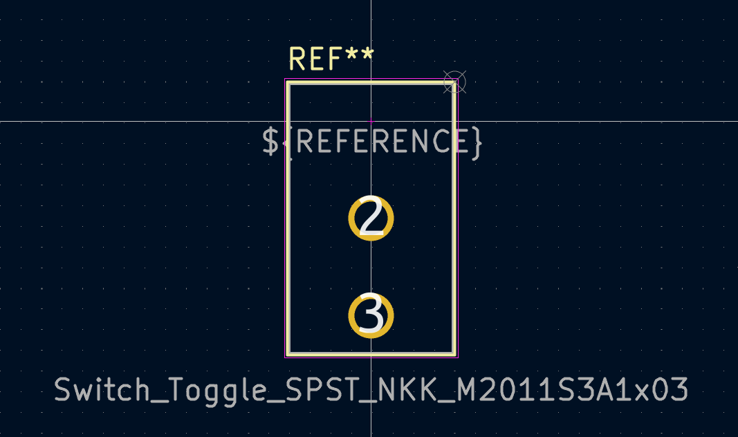
Dopo aver completato i contorni, posizionare il testo come mostrato di seguito. L’impronta è completa.
Convenzioni librerie KiCad
Per mantenere librerie di simboli e impronte di alta qualità, KiCad ha un documento KiCad Library Conventions, che è un set di linee guida per simboli e impronte. Non è necessario seguire queste convenzioni per le librerie personali, ma sono un buon punto di partenza. Le impronte e i simboli nella biblioteca ufficiale devono seguire KLC. KLC è usato come base per i simboli e le impronte presenti in questa guida.
Add switch to schematic
Ora che l’impronta è completa, il simbolo dell’interruttore può essere modificato in modo che per impostazione predefinita venga utilizzato l’impronta corrispondente.
Tornare all’editor dei simboli e aprire il simbolo dell’interruttore. Modificare le proprietà del simbolo. Fare clic nel campo Impronta, poi fare clic sull’icona a forma di libro della libreria  che appare. Sfogliare la libreria delle impronte del progetto e fare doppio clic sull’impronta dell’interruttore. Salvare il simbolo.
Ora l’impronta dell’interruttore è assegnata a questo simbolo per impostazione predefinita; non è necessario selezionarla manualmente ogni volta che il simbolo viene aggiunto a uno schema.
Aprire lo schema, aggiungere un nuovo simbolo e selezionare il nuovo simbolo dell’interruttore. Allacciarlo per connettere o sconnettere il LED alla batteria.
Non è necessario scegliere manualmente un’impronta per l’interruttore, perché il simbolo dell’interruttore specifica già un’impronta. Eseguire l’ERC per assicurarsi che lo schema modificato non violi alcuna regola elettrica.
Add switch to layout
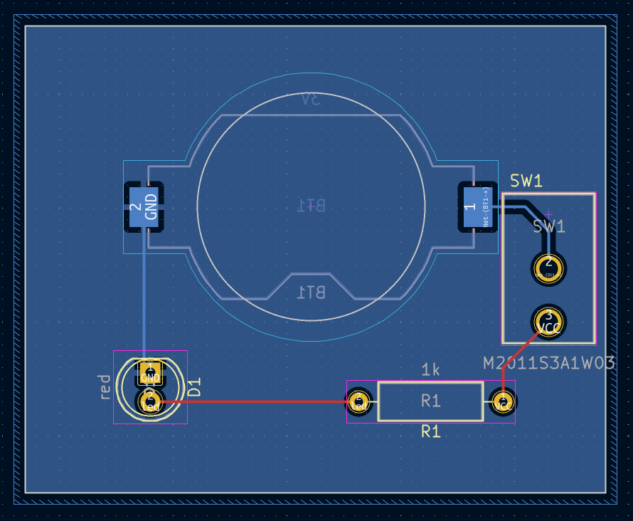
Assicurarsi di aver salvato lo schema, poi aprire l’editor scheda per aggiungere il simbolo al progetto. Aggiornare il circuito stampato con le modifiche allo schema usando Strumenti → Aggiorna C.S. dallo schema… e posizionare l’impronta dell’interruttore sulla scheda come mostrato. Se necessario, ridimensionare il bordo della scheda e la zona rame (la zona rame non verrà svuotata se ridimensionata, ma è possibile riempirla nuovamente se necessario con B).
La ratsnest mostra le nuove connessioni da sbrogliare. Inoltre, la connessione tra la batteria e la resistenza deve essere eliminata.
Per primo, eliminare le piste non necessarie. Selezionare una delle piste tra la batteria e la resistenza, non importa quale. Premere U più volte per espandere la selezione e includere tutti i segmenti tra la batteria e la resistenza. Premere Canc per rimuovere la connessione.
Sbrogliare le nuove piste tra la batteria e l’interruttore e tra l’interruttore e la resistenza. Premere B per riempire nuovamente le zone.
Infine, rieseguire un test DRC per assicurarsi che la scheda modificata non violi alcuna regola di progettazione.
Linking symbols, footprints, and 3D models
Symbols and footprints
Come descritto nella sezione assegnazione dell’impronta, a ogni simbolo nello schema deve essere assegnata una impronta durante il processo di inserimento dello schema. Il nome dell’impronta assegnata a ogni simbolo viene memorizzato nel campo Impronta delle proprietà del simbolo.
I simboli possono specificare un’impronta preselezionata. Le impronte non devono necessariamente essere assegnate manualmente a tali simboli, poiché un’impronta era già stata scelta durante la creazione del simbolo. Gli utenti possono sovrascrivere l’impronta preselezionata durante il processo di assegnazione dell’impronta come di consueto. Definire un’impronta predefinita è una buona idea per i simboli a cui solitamente o quasi sempre verrà assegnata la stessa impronta, ad esempio un componente che è disponibile solo per un tipo specifico di package. L’impronta dell’interruttore predefinita era stata impostata come predefinita per il suo simbolo corrispondente.
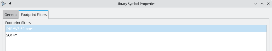
I simboli possono anche specificare filtri impronte, che possono essere utilizzati per nascondere le impronte incompatibili con il simbolo. Ad esempio, il simbolo 74HC00 ha filtri impronte che determinano la visualizzazione solo di impronte DIP e SO14 applicabili nello strumento di assegnamento impronte.
I requisiti KLC per filtri impronte contengono alcuni suggerimenti utili per creare dei filtri impronte efficaci.
Footprints and 3D models
I modelli 3D per i componenti vengono archiviati in file separati. I nomi file per i modelli 3D dei componenti vengono salvati nell’impronta. È possibile aggiungere un numero qualsiasi di modelli 3D ad ogni impronta. I nomi file dei modelli 3D, insieme a scala del modello, rotazione, scostamento e opacità, sono impostati nella scheda Modelli 3D delle Proprietà dell’impronta.
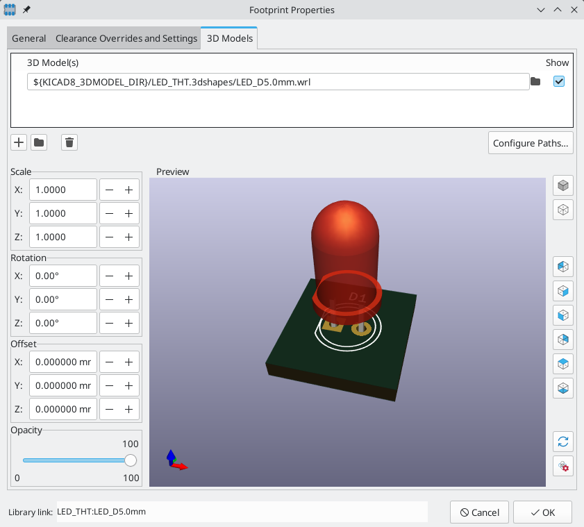
Both STEP (.step) and VRML (.wrl) 3D model formats are supported. STEP files are useful where dimensional accuracy is needed, while VRML files can be used for more visually attractive renders. Many footprints in KiCad’s library have associated 3D models; these models are provided in STEP format.
| Non tutte le impronte nella libreria di KiCad sono fornite di modelli 3D, ma tutti le impronte elencano un nome file di modello 3D anche se il modello 3D non esiste. Questo perché i modelli 3D potrebbero essere aggiunti in un secondo momento senza dover modificare l’impronta. |
FreeCAD together with the StepUp Workbench are useful for creating component 3D models; they are used for many of the models in KiCad’s library. StepUp is used to generate STEP and VRML files with correct placement, scaling, and rotation.
Where to go from here
More learning resources
Per maggiori informazioni su come utilizzare KiCad, consultare il manuale.
Altre risorse includono il forum ufficiale degli utenti di KiCad, le chat Discord o IRC e ulteriori risorse di apprendimento dalla comunità KiCad.
Per scoprire di più sulle possibilità offerte da KiCad, visitare la sezione Made With KiCad del sito web oppure aprire i progetti demo inclusi in KiCad (File → Apri progetto demo…).
Help improve KiCad
Per segnalare un difetto o richiedere una funzionalità, usare Aiuto → Segnala un difetto o aprire una segnalazione su Gitlab.
Per contribuire allo sviluppo di KiCad, consultare la pagina dei contributi degli sviluppatori. Anche i semplici utenti possono aiutare contribuendo allo sviluppo delle librerie o della documentazione e traduzione. Infine, si consideri il supporto finanziariario per mantenere in modo continuo lo sviluppo di KiCad.