Manual de referencia
Copyright
This document is Copyright © 2010-2018 by its contributors as listed below. You may distribute it and/or modify it under the terms of either the GNU General Public License (http://www.gnu.org/licenses/gpl.html), version 3 or later, or the Creative Commons Attribution License (http://creativecommons.org/licenses/by/3.0/), version 3.0 or later.
Todas las marcas mencionadas en esta guía pertenecen a sus legítimos propietarios.
Contribuidores
Jean-Pierre Charras, Fabrizio Tappero.
Traducción
Antonio Morales <[email protected]>, 2015
Realimentación
Por favor dirija cualquier reporte de fallo, sugerencia o nuevas versiones a:
-
Acerca de la documentación de KiCad: https://gitlab.com/kicad/services/kicad-doc/issues
-
Acerca del software KiCad: https://gitlab.com/kicad/code/kicad/issues
-
About KiCad translation: https://gitlab.com/kicad/code/kicad-i18n/issues
Fecha de publicación y versión del software
Published on May 30, 2015.
Introducción a Eeschema
Descripción
Eeschema is a schematic capture software distributed as a part of KiCad and available under the following operating systems:
-
Linux
-
Apple macOS
-
Windows
Indistintamente del SO, todos los ficheros de Eeschema son 100% compatibles de un SO a otro.
Eeschema es una aplicación integrada donde todas las funciones para el dibujado, control, planos, gestión de bibliotecas y acceso al software de diseño del PCB son llevadas a cabo dentro del propio Eeschema.
Eeschema is intended to cooperate with PcbNew, which is KiCad’s printed circuit design software. It can also export netlist files, which lists all the electrical connections, for other packages.
Eeschema includes a symbol library editor, which can create and edit symbols and manage libraries. It also integrates the following additional but essential functions needed for modern schematic capture software:
-
Comprobador de reglas eléctricas (ERC) para el control automático de conexiones incorrectas y/o perdidas.
-
Exportación de ficheros de plano en múltiples formatos (Postscript, PDF, HPGL y SVG)
-
Bill of Materials generation (via Python or XSLT scripts, which allow many flexible formats).
Resumen técnico
Eeschema is limited only by the available memory. There is thus no real limitation to the number of components, component pins, connections or sheets. In the case of multi-sheet diagrams, the representation is hierarchical.
Eeschema can use multi-sheet diagrams in a few ways:
-
Jerarquías simples (cada esquemas es usado solo una vez)
-
Jerarquías complejas (algunos esquemas son usados mas de una vez con múltiples instancias)
-
Jerarquías planas (los esquemas no están explícitamente conectados en el esquema principal)
Comandos Generales de Eeschema
Commands can be executed by:
-
Haciendo clic en la barra de menú (parte superior de la pantalla)
-
Haciendo clic sobre los iconos de la parte superior de la pantalla (comandos generales)
-
Haciendo clic sobre los iconos de la parte derecha de la pantalla (comandos particulares o "herramientas")
-
Haciendo clic sobre los iconos de la pare izquierda de la pantalla (opciones de visualización)
-
Presionando los botones del ratón (importantes comandos complementarios). En particular un clic derecho del ratón abre el menú contextual del elemento bajo el cursor (Zoom, rejilla y edición de elementos)
-
Function keys (F1, F2, F3, F4, Insert and Space keys). Specifically: Escape key cancels the command in progress. Insert key allows the duplication of the last element created.
-
Pressing hot keys which typically perform a select tool command and begin tool action at the current cursor location. For a list of hot keys, see the "Help→List Hotkeys" menu entry or press 'Ctrl+F1' key.
Comandos del Raton
Comandos Básicos
Botón Izquierdo
-
Single click: displays the characteristics of the symbol or text under the cursor in the status bar.
-
Double click: edit (if the element is editable) the symbol or text.
Botón derecho
-
Abre un menú emergente.
Block operations
Puede mover, arrastrar, copiar y borrar áreas seleccionadas en todos los menús de Eeschema.
Areas are selected by drawing a box around items using the left mouse button.
Holding Shift'', Ctrl'', or ``Shift + Ctrl'' during selection respectively performs copying, dragging and deletion:
botón izquierdo del ratón |
Mueve la selección. |
Shift + botón izquierdo del ratón |
Copia la selección. |
Ctrl + botón izquierdo del ratón |
Arrastra la selección. |
Ctrl + Shift + botón izquierdo del ratón |
Borra la selección. |
Cuando copie o arrastre, puede:
-
Hacer clic de nuevo para colocar los elementos.
-
Click the right button or press Escape key to cancel.
If a block move command has started, another command can be selected using the right-click pop-up menu.
Teclas rápidas
-
La tecla Ctrl+F1 muestra la lista de teclas rápidas actual
-
Hotkeys might be redefined in Controls tab of Schematic Editor Options dialog (menu Preferences → General Options).
Here is the default hotkey list:
Help (this window) |
Ctrl+F1 |
Zoom In |
F1 |
Zoom Out |
F2 |
Zoom Redraw |
F3 |
Zoom Center |
F4 |
Fit on Screen |
Home |
Zoom to Selection |
@ |
Reset Local Coordinates |
Space |
Edit Item |
E |
Delete Item |
Del |
Rotate Item |
R |
Drag Item |
G |
Undo |
Ctrl+Z |
Redo |
Ctrl+Y |
Mouse Left Click |
Return |
Mouse Left Double Click |
End |
Save Schematic |
Ctrl+S |
Load Schematic |
Ctrl+O |
Find Item |
Ctrl+F |
Find Next Item |
F5 |
Find Next DRC Marker |
Shift+F5 |
Find and Replace |
Ctrl+Alt+F |
Repeat Last Item |
Ins |
Move Block → Drag Block |
Tab |
Copy Block |
Ctrl+C |
Paste Block |
Ctrl+V |
Cut Block |
Ctrl+X |
Move Schematic Item |
M |
Duplicate Symbol or Label |
C |
Add Symbol |
A |
Add Power |
P |
Mirror X |
X |
Mirror Y |
Y |
Orient Normal Symbol |
N |
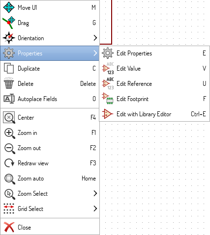
Edit Symbol Value |
V |
Edit Symbol Reference |
U |
Edit Symbol Footprint |
F |
Edit with Symbol Editor |
Ctrl+E |
Begin Wire |
W |
Begin Bus |
B |
End Line Wire Bus |
K |
Add Label |
L |
Add Hierarchical Label |
H |
Add Global Label |
Ctrl+L |
Add Junction |
J |
Add No Connect Flag |
Q |
Add Sheet |
S |
Add Wire Entry |
Z |
Add Bus Entry |
/ |
Add Graphic PolyLine |
I |
Add Graphic Text |
T |
Update PCB from Schematic |
F8 |
Autoplace Fields |
O |
Leave Sheet |
Alt+BkSp |
Delete Node |
BkSp |
Highlight Connection |
Ctrl+X |
All hotkeys can be redefined using the hotkey editor (menu Preferences→General Options→Controls).
It is possible to import/export hotkey settings using menu Preferences→Import and Export→Import/Export Hotkeys.
Grid
In Eeschema the cursor always moves over a grid. The grid can be customized:
-
Size might be changed using the pop-up menu or using the Preferences/Options menu.
-
Color might be changed in Colors tab of the Schematic Editor Options dialog (menu Preferences → General Options).
-
Visibility might be switched using the left-hand toolbar button.
El tamaño por defecto de la rejilla es de 50 mil (0.050") o 1,27 milímetros.
This is the preferred grid to place symbols and wires in a schematic, and to place pins when designing a symbol in the Symbol Editor.
One can also work with a smaller grid from 25 mil to 10 mil. This is only intended for designing the symbol body or placing text and comments and not recommended for placing pins and wires.
Selección del Zoom
Para cambiar el nivel de zoom:
-
El botón derecho abre el menú contextual y permite seleccionar el zoom deseado.
-
O use las teclas de función:
-
F1: Zoom in
-
F2: Zoom out
-
F4 or simply click on the middle mouse button (without moving the mouse): Center the view around the cursor pointer position
-
-
Zoom sobre la ventana:
-
Mouse wheel: Zoom in/out
-
Shift+Mouse wheel: Pan up/down
-
Ctrl+Mouse wheel: Pan left/right
-
Mostrando las coordenadas del cursor
The display units are in inches or millimeters. However, Eeschema always uses 0.001 inch (mil/thou) as its internal unit.
La siguiente información se muestra en la parte inferior derecha de la pantalla.
-
El factor de zoom
-
La posición absoluta del cursor
-
La posición relativa del cursor
The relative coordinates can be reset to zero by pressing Space. This is useful for measuring distance between two points or aligning objects.

Barra de menú superior
The top menu bar allows the opening and saving of schematics, program configuration and viewing the documentation.

Barra de herramientas superior
Esta barra de herramientas permite el acceso a las principales funciones de Eeschema.
Si se ejecuta Eeschema de modo independiente, este es el conjunto de herramientas disponible:

Note that when KiCad runs in project mode, the first two icons are not available as they work with individual files.
|
Create a new schematic (only in standalone mode). |
|
Open a schematic (only in standalone mode). |
|
Save complete schematic project. |
|
Select the sheet size and edit the title block. |
|
Open print dialog. |
|
Paste a copied/cut item or block to the current sheet. |
|
Undo: Revert the last change. |
|
Redo: Revert the last undo operation. |
|
Show the dialog to search symbols and texts in the schematic. |
|
Show the dialog to search and replace texts in the schematic. |
|
Refresh screen; zoom to fit. |
|
Zoom in and out. |
|
View and navigate the hierarchy tree. |
|
Leave the current sheet and go up in the hierarchy. |
|
Call the symbol library editor to view and modify libraries and symbols. |
|
Browse symbol libraries. |
|
Annotate symbols. |
|
Electrical Rules Checker (ERC), automatically validate electrical connections. |
|
Call CvPcb to assign footprints to symbols. |
|
Export a netlist (Pcbnew, SPICE and other formats). |
|
Edit symbol fields. |
|
Generate the Bill of Materials (BOM). |
|
Call Pcbnew to perform a PCB layout. |
|
Back-import footprint assignment (selected using CvPcb or Pcbnew) into the "footprint" fields. |
Iconos de la barra de herramientas derecha.
Esta barra de herramientas contiene herramientas para:
-
Place symbols, wires, buses, junctions, labels, text, etc.
-
Create hierarchical subsheets and connection symbols.
|
Cancel the active command or tool. |
|
Highlight a net by marking its wires and net labels with a different color. If KiCad runs in project mode then copper corresponding to the selected net will be highlighted in Pcbnew as well. |
|
Display the symbol selector dialog to select a new symbol to be placed. |
|
Display the power symbol selector dialog to select a power symbol to be placed. |
|
Draw a wire. |
|
Draw a bus. |
|
Draw wire-to-bus entry points. These elements are only graphical and do not create a connection, thus they should not be used to connect wires together. |
|
Draw bus-to-bus entry points. |
|
Place a "No Connect" flag. These flags should be placed on symbol pins which are meant to be left unconnected. It is done to notify the Electrical Rules Checker that lack of connection for a particular pin is intentional and should not be reported. |
|
Place a junction. This connects two crossing wires or a wire and a pin, when it can be ambiguous (i.e. if a wire end or a pin is not directly connected to another wire end). |
|
Place a local label. Local label connects items located in the same sheet. For connections between two different sheets, you have to use global or hierarchical labels. |
|
Place a global label. All global labels with the same name are connected, even when located on different sheets. |
|
Place a hierarchical label. Hierarchical labels are used to create a connection between a subsheet and the parent sheet that contains it. |
|
Place a hierarchical subsheet. You must specify the file name for this subsheet. |
|
Import a hierarchical pin from a subsheet. This command can be executed only on hierarchical subsheets. It will create hierarchical pins corresponding to hierarchical labels placed in the target subsheet. |
|
Place a hierarchical pin in a subsheet. This command can be executed only on hierarchical subsheets. It will create arbitrary hierarchical pins, even if they do not exist in the target subsheet. |
|
Draw a line. These are only graphical and do not connect anything. |
|
Place a text comment. |
|
Place a bitmap image. |
|
Delete selected element. |
Iconos de la barra de herramientas izquierda
Esta barra de herramientas gestiona las opciones de visualización:
|
Toggle grid visibility. |
|
Switch units to inches. |
|
Switch units to millimeters. |
|
Choose the cursor shape (full screen/small). |
|
Toggle visibility of "invisible" pins. |
|
Toggle free angle/90 degrees wires and buses placement. |
Menús emergentes y de edición rápida
Un clic con el botón derecho abre un menú contextual para el elemento seleccionado. Este contiene:
-
Factor de zoom.
-
Ajuste de la rejilla.
-
Parámetros comúnmente editados del elemento seleccionado.
Menú emergente sin elemento seleccionado.
Editing a label.
Editing a symbol.
Menú principal superior
Menú archivo
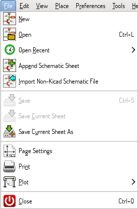
| New | Close current schematic and start a new one (only in standalone mode). |
|---|---|
Open |
Load a schematic project (only in standalone mode). |
Open Recent |
Open a schematic project from the list of recently opened files (only in standalone mode). |
Append Schematic Sheet |
Insert the contents of another sheet into the current one. |
Import Non-Kicad Schematic File |
Imports a schematic project saved in another file format. |
Save |
Save current sheet and all its subsheets. |
Save Current Sheet |
Save only the current sheet, but not others in the project. |
Save Current Sheet As… |
Save the current sheet under a new name. |
Page Settings |
Configure page dimensions and title block. |
Print schematic project (See also chapter Plot and Print). |
|
Plot |
Export to PDF, PostScript, HPGL or SVG format (See chapter Plot and Print). |
Close |
Terminate the application. |
Menú Preferencias
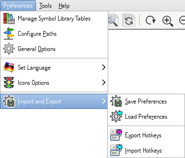
Manage Symbol Library Tables |
Add/remove symbol libraries. |
Configure Paths |
Set the default search paths. |
General Options |
Preferences (units, grid size, field names, etc.). |
Set Language |
Select interface language. |
Icons Options |
Icons visibility settings. |
Import and Export |
Transfer preferences to/from file. |
Manage Symbol Library Tables
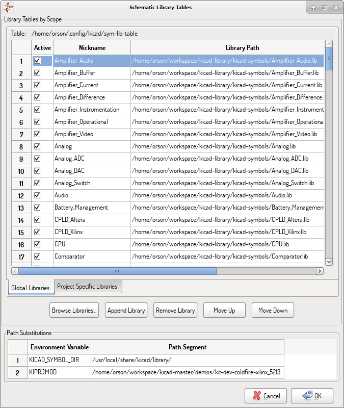
Eeschema uses two library tables to store the list of available symbol libraries, which differ by the scope:
-
Global Libraries
Libraries listed in the Global Libraries table are available to every project. They are saved in sym-lib-table in your home directory (exact path is dependent on the operating system; check the path above the table).
-
Project Specific Libraries
Libraries listed in Project Specific Libraries table are available to the currently opened project. They are saved in sym-lib-table file in the project directory (check the path above the table).
You can view either list by clicking on "Global Libraries" or "Project Specific Libraries" tab below the library table.
Add a new library
Add a library either by clicking Browse Libraries… button and selecting a file or clicking "Append Library" and typing a path to a library file. The selected library will be added to the currently opened library table (Global/Project Specific).
Remove a library
Remove a library by selecting one or more libraries and clicking Remove Library button.
Library properties
Each row in the table stores several fields describing a library:
Active |
Enables/disables the library. It is useful to temporarily reduce the loaded library set. |
Nickname |
Nickname is a short, unique identifier used for assigning symbols to components. Symbols are represented by '<Library Nickname>:<Symbol Name>' strings. |
Library Path |
Path points to the library location. |
Plugin Type |
Determines the library file format. |
Options |
Stores library specific options, if used by plugin. |
Description |
Briefly characterizes the library contents. |
General Options
Display
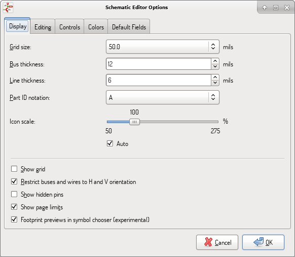
Grid Size |
Grid size selection. It is recommended to work with normal grid (0.050 inches or 1,27 mm). Smaller grids are used for component building. |
Bus thickness |
Pen size used to draw buses. |
Line thickness |
Pen size used to draw objects that do not have a specified pen size. |
Part ID notation |
Style of suffix that is used to denote symbol units (U1A, U1.A, U1-1, etc.) |
Icon scale |
Adjust toolbar icons size. |
Show Grid |
Grid visibility setting. |
Restrict buses and wires to H and V orientation |
If checked, buses and wires are drawn only with vertical or horizontal lines. Otherwise buses and wires can be placed at any orientation. |
Show hidden pins: |
Display invisible (or hidden) pins, typically power pins. |
Show page limits |
If checked, shows the page boundaries on screen. |
Footprint previews in symbol chooser |
Displays a footprint preview frame and footprint selector when placing a new symbol. Note: it may cause problems or delays, use at your own risk. |
Editing
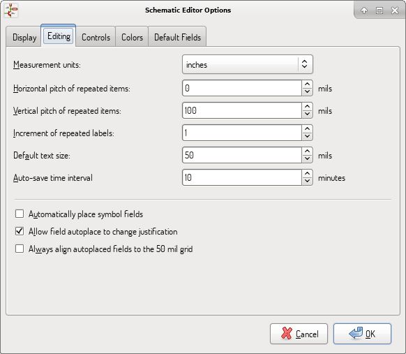
Measurement units |
Select the display and the cursor coordinate units (inches or millimeters). |
Horizontal pitch of repeated items |
Increment on X axis during element duplication (default: 0) (after placing an item like a symbol, label or wire, a duplication is made by the Insert key) |
Vertical pitch of repeated items |
Increment on Y axis during element duplication (default: 0.100 inches or 2,54 mm). |
Increment of repeated labels |
Increment of label value during duplication of texts ending in a number, such as bus members (usual value 1 or -1). |
Default text size |
Text size used when creating new text items or labels. |
Auto-save time interval |
Time in minutes between saving backups. |
Automatically place symbol fields |
If checked, symbol fields (e.g. value and reference) in newly placed symbols might be moved to avoid collisions with other items. |
Allow field autoplace to change justification |
Extension of 'Automatically place symbol fields' option. Enable text justification adjustment for symbol fields when placing a new part. |
Always align autoplaced fields to the 50 mil grid |
Extension of 'Automatically place symbol fields' option. If checked, fields are autoplaced using 50 mils grid, otherwise they are placed freely. |
Controls
Redefine hotkeys and set up the user interface behavior.
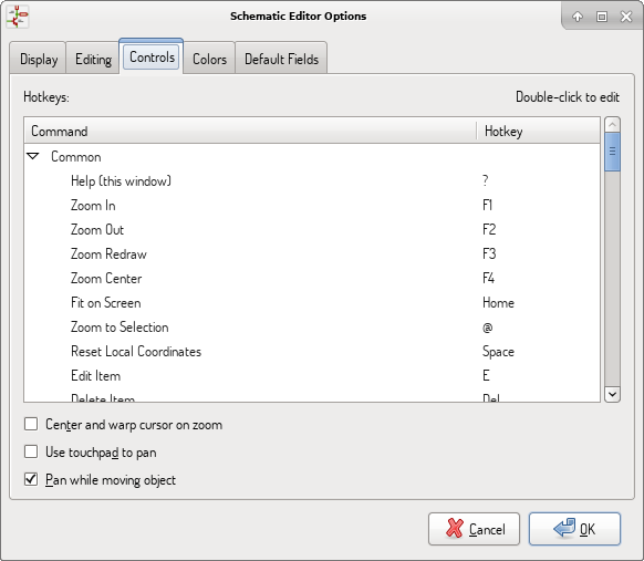
Select a new hotkey by double clicking an action or right click on an action to show a popup menu:
Edit |
Define a new hotkey for the action (same as double click). |
Undo Changes |
Reverts the recent hotkey changes for the action. |
Restore Default |
Sets the action hotkey to its default value. |
Undo All Changes |
Reverts all recent hotkey changes for the action. |
Restore All to Default |
Sets all action hotkeys to their default values. |
Options description:
Center and warp cursor on zoom |
If checked, the pointed location is warped to the screen center when zooming in/out. |
Use touchpad to pan |
When enabled, view is panned using scroll wheels (or touchpad gestures) and to zoom one needs to hold Ctrl. Otherwise scroll wheels zoom in/out and Ctrl/Shift are the panning modifiers. |
Pan while moving object |
If checked, automatically pans the window if the cursor leaves the window during drawing or moving. |
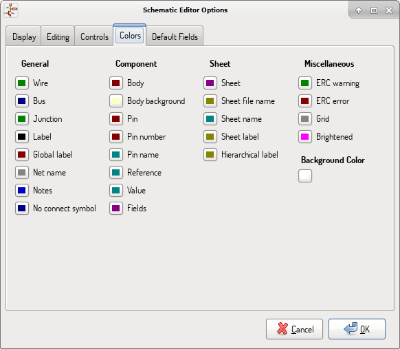
Colors
Color scheme for various graphic elements. Click on any of the color swatches to select a new color for a particular element.
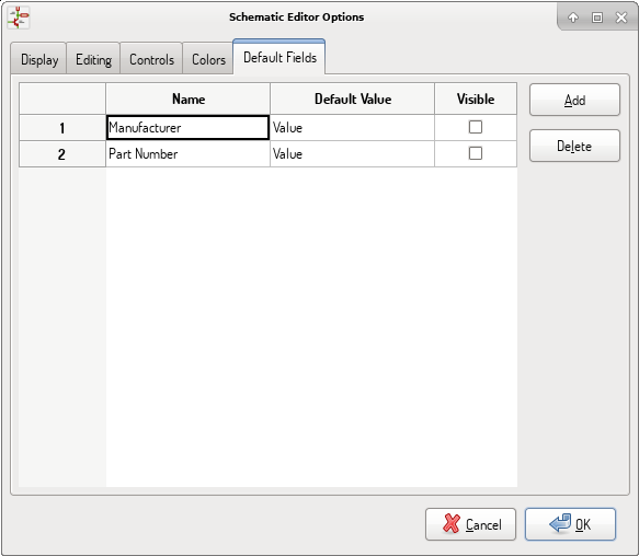
Default Fields
Define additional custom fields and corresponding values that will appear in newly placed symbols.
Menú ayuda
Access to on-line help (this document) for an extensive tutorial about KiCad.
Use ``Copy Version Information'' when submitting bug reports to identify your build and system.
Barra de Herramientas de uso general
Gestión de hoja
The Sheet Settings icon (![]() ) allows you to define the sheet size and the contents of the title block.
) allows you to define the sheet size and the contents of the title block.
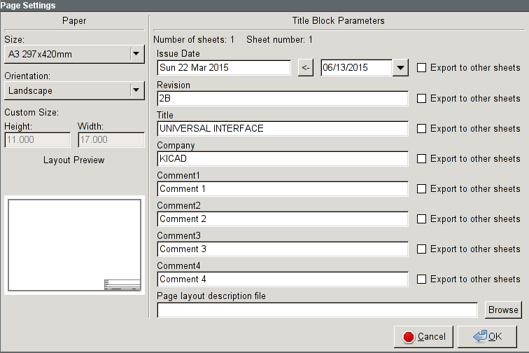
El numerado de las hojas se actualiza automáticamente. Puede ajustar la fecha actual presionando el botón a la derecha de "Issue Date", pero esto no se actualizará automáticamente.
Herramienta de Busqueda
The Find icon (![]() ) can be used to access the search tool.
) can be used to access the search tool.
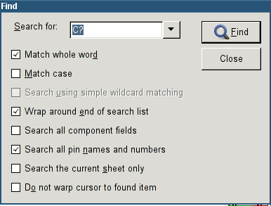
You can search for a reference, a value or a text string in the current sheet or in the whole hierarchy. Once found, the cursor will be positioned on the found element in the relevant sub-sheet.
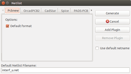
Herramienta de Netlist
The Netlist icon (![]() ) opens the netlist generation tool.
) opens the netlist generation tool.
The tool creates a file which describe all connections in the entire hierarchy.
In a multisheet hierarchy, any local label is visible only inside the sheet to which it belongs. For example: the label LABEL1 of sheet 3 is different from the label LABEL1 of sheet 5 (if no connection has been intentionally introduced to connect them). This is due to the fact that the sheet name path is internally associated with the local label.
| Even though there is no text length limit for labels in Eeschema, please take into account that other programs reading the generated netlist may have such constraints. |
| Avoid spaces in labels, because they will appear as separated words in the generated file. It is not a limitation of Eeschema, but of many netlist formats, which often assume that a label has no spaces. |
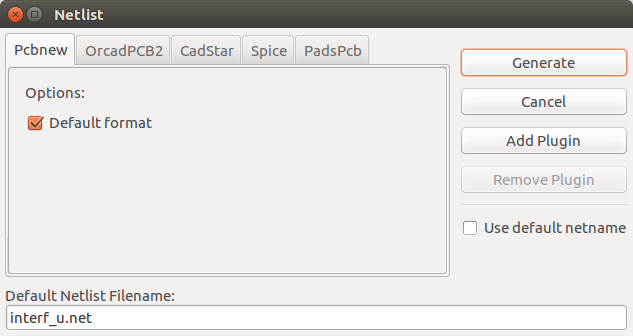
Opciones:
Default Format |
Check to select Pcbnew as the default format. |
También se pueden generar otros formatos:
-
Orcad PCB2
-
CadStar
-
Spice (simulators)
External plugins can be added to extend the netlist formats list (PadsPcb Plugin was added in the picture above).
There is more information about creating netlists in Create a Netlist chapter.
Herramienta de Anotado
The icon ![]() launches the annotation tool. This tool assigns references to components.
launches the annotation tool. This tool assigns references to components.
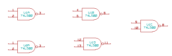
Para componentes multi-parte (como el 7400 TTL que contiene 4 puertas), un sufijo multi-parte es añadido (así un 7400 TTL designado como U3 será dividido en U3A, U3B, U3C y U3D).
You can unconditionally annotate all the components or only the new components, i.e. those which were not previously annotated.
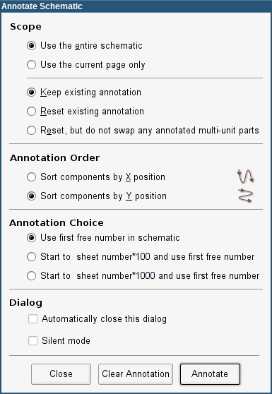
Alcance
| Use the entire schematic | All sheets are re-annotated (default). |
|---|---|
Use the current page only |
Only the current sheet is re-annotated (this option is to be used only in special cases, for example to evaluate the amount of resistors in the current sheet.). |
Keep existing annotation |
Conditional annotation, only the new components will be re-annotated (default). |
Reset existing annotation |
Unconditional annotation, all the components will be re-annotated (this option is to be used when there are duplicated references). |
Reset, but do not swap any annotated multi-unit parts |
Keeps all groups of multiple units (e.g. U2A, U2B) together when reannotating. |
Orden de Anotado
Selects the order in which components will be numbered (either horizontally or vertically).
Tipo de Anotado
Selects the assigned reference format.
Herramienta de Comprobación de Reglas Eléctricas
The icon ![]() launches the electrical rules check (ERC) tool.
launches the electrical rules check (ERC) tool.
This tool performs a design verification and is able to detect forgotten connections, and inconsistencies.
Once you have run the ERC, Eeschema places markers to highlight problems. The error description is displayed after left clicking on the marker. An error report file can also be generated.
Ventana principal del ERC
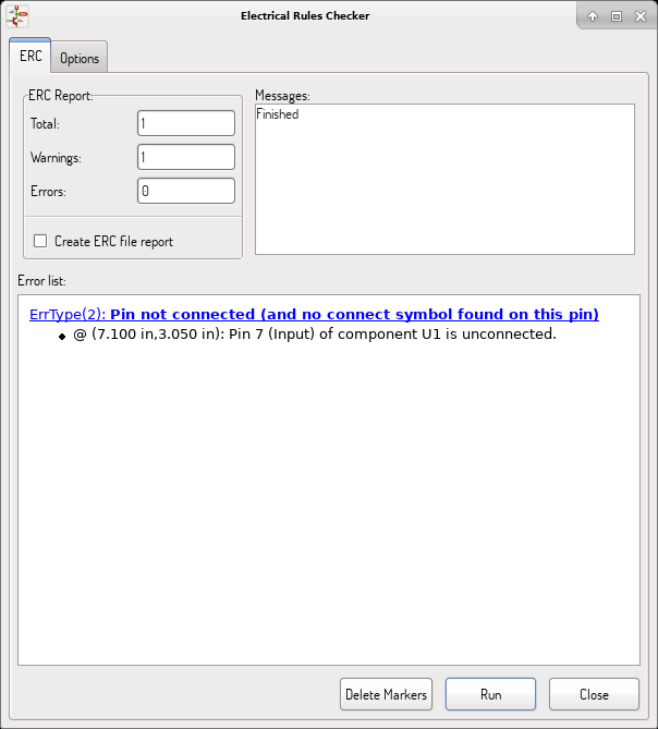
Errors are displayed in the Electrical Rules Checker dialog:
-
Número total de errores y avisos.
-
Número de errores.
-
Número de avisos.
Opciones:
Create ERC file report |
Check this option to generate an ERC report file. |
Comandos:
Delete Markers |
Remove all ERC error/warnings markers. |
Run |
Start an Electrical Rules Check. |
Close |
Close the dialog. |
-
Haciendo clic sobre un mensaje de error se salta a la marca correspondiente en el esquema.
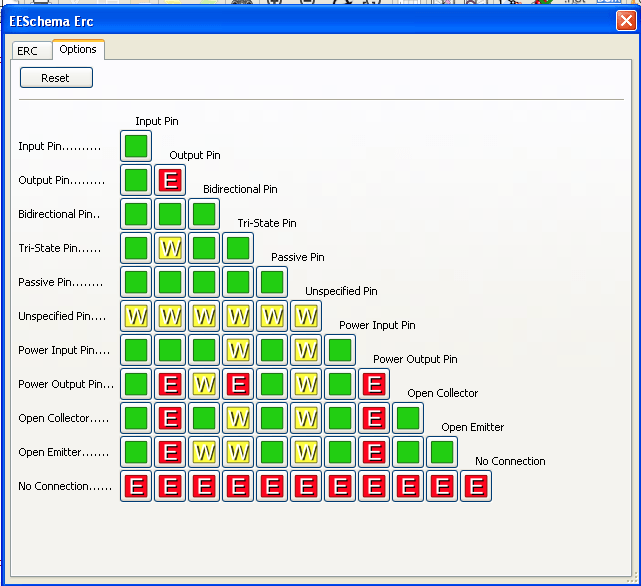
Ventana de opciones del ERC
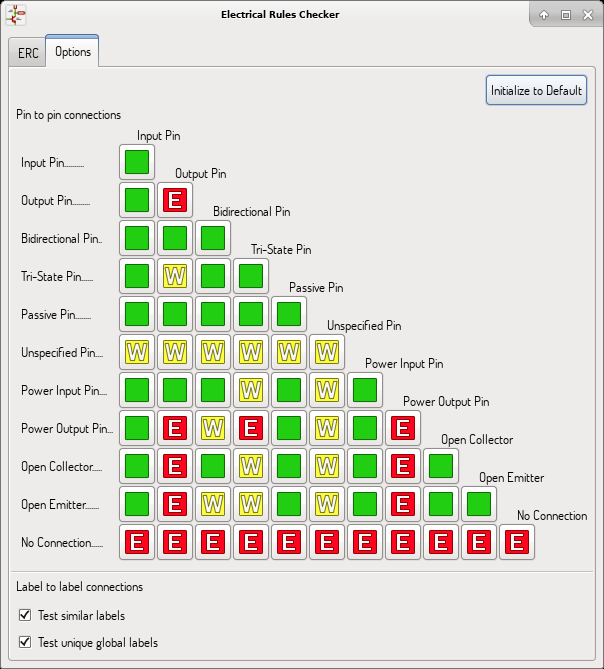
This tab allows you to define the connectivity rules between pins; you can choose between 3 options for each case:
-
Sin error
-
Aviso
-
Error
Cada cuadro de la matriz puede ser modificado haciendo clic en el.
Opciones:
Test similar labels |
Report labels that differ only by letter case (e.g. label/Label/LaBeL). Net names are case-sensitive therefore such labels are treated as separate nets. |
Test unique global labels |
Report global lables that occur only once for a particular net. Normally it is required to have at least two make a connection. |
Comandos:
Initialize to Default |
Restores the original settings. |
Herramienta Lista de Materiales
The icon ![]() launches the bill of materials (BOM) generator. This tool generates a file listing the components and/or hierarchical connections (global labels).
launches the bill of materials (BOM) generator. This tool generates a file listing the components and/or hierarchical connections (global labels).
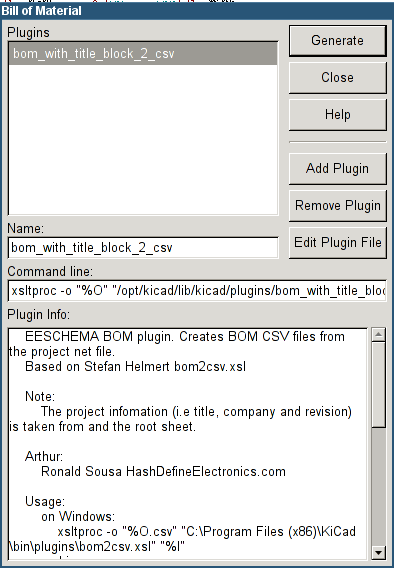
Eeschema’s BOM generator makes use of external plugins, either as XSLT or Python scripts. There are a few examples installed inside the KiCad program files directory.
Un conjunto de propiedades de componente útil para usar en un listado BOM son:
-
Valor - nombre único para cada componente usado.
-
Huella - tanto asignada manualmente como anotada de vuelta (ver abajo)
-
Campo1 - Nombre del fabricante
-
Campo2 - Número de referencia del Fabricante.
-
Campo3 - Número de referencia del Distribuidor.
Por ejemplo:
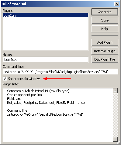
On MS Windows, BOM generator dialog has a special option (pointed by red arrow) that controls visibility of external plugin window. + By default, BOM generator command is executed console window hidden and output is redirected to Plugin info field. Set this option to show the window of the running command. It may be necessary if plugin has provides a graphical user interface.
Edit Fields tool
The icon ![]() opens a spreadsheet to view and modify field values for all symbols.
opens a spreadsheet to view and modify field values for all symbols.
Once you modify field values, you need to either accept changes by clicking on 'Apply' button or undo them by clicking on 'Revert' button.
Tricks to simplify fields filling
There are several special copy/paste methods in spreadsheet. They may be useful when entering field values that are repeated in a few components.
These methods are illustrated below.
| Copy (Ctrl+C) | Selection | Paste (Ctrl+V) |
|---|---|---|
|
|
|
|
|
|
|
|
|
|
|
|
|
|
|
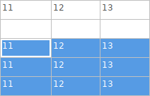
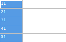
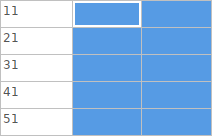
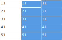
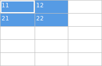
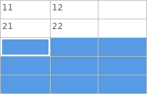
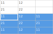
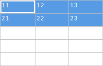
| These techniques are also available in other dialogs with a grid control element. |
Import tool for footprint assignment
Acceso:
The icon ![]() launches the back-annotate tool.
launches the back-annotate tool.
Esta herramienta permite que los cambios en las asignaciones de huellas realizadas en PcbNew puedan ser importados de vuelta a los campos correspondientes en Eeschema.
Manage Symbol Libraries
Symbol libraries hold collections of symbols used when creating schematics. Each symbol in a schematic is uniquely identified by a full name that is composed of a library nickname and a symbol name. An example is Audio:AD1853.
Symbol Library Table
The symbol library table holds a list of all library files KiCad knows about. The symbol library table is constructed from the global symbol library table file and the project specific symbol library table file.
When a symbol is loaded, Eeschema uses the library nickname, Audio in our example, to lookup the library location in the symbol library table.
The image below shows the symbol library table editing dialog which can be opened by invoking the Manage Symbol Library Tables'' entry in the Preferences'' menu.
Global Symbol Library Table
The global symbol library table contains the list of libraries that are always available regardless of the currently loaded project file. The table is saved in the file sym-lib-table in the user’s home folder. The location of this folder is dependent upon the operating system being used.
Project Specific Symbol Library Table
The project specific symbol library table contains the list of libraries that are available specifically for the currently loaded project file. The project specific symbol library table can only be edited when it is loaded along with the project file. If no project file is loaded or there is no symbol library table file in the current project path, an empty table is created which can be edited and later saved along with the project file.
Initial Configuration
The first time Eeschema is run and the global symbol table file sym-lib-table is not found in the user’s home folder, Eeschema will attempt to copy the default symbol table file sym-lib-table stored in the system’s KiCad template folder to the file sym-lib-table in the user’s home folder. If the default template sym-lib-table file cannot be found, a dialog will prompt for an alternate location for the sym-lib-table file. If no sym-lib-table is found or the dialog is dismissed, an empty symbol library table will be created in the user’s home folder. If this happens, the user can either copy sym-lib-table manually or configure the table by hand.
|
The default symbol library table includes all of the symbol libraries that are installed as part of KiCad. This may or may not be desirable depending on usages and the speed of the system. The amount of time required to load the symbol libraries is proportional to the number of libraries in the symbol library table. If symbol library load times are excessive, remove rarely and/or never used libraries from the global library table and add them to the project library table as required. |
Adding Table Entries
In order to use a symbol library, it must first be added to either the global table or the project specific table. The project specific table is only applicable when you have a project file open.
Each library entry must have a unique nickname.
This does not have to be related in any way to the actual library file name or path. The colon ':' and '/' characters cannot be used anywhere in the library nickname. Each library entry must have a valid path and/or file name depending on the type of library. Paths can be defined as absolute, relative, or by environment variable substitution (see section below).
The appropriate plug in type must be selected in order for the library to be properly read. KiCad currently supports only legacy symbol library files plug-in.
There is also a description field to add a description of the library entry. The option field is not used at this time so adding options will have no effect when loading libraries.
-
Please note that you cannot have duplicate library nicknames in the same table. However, you can have duplicate library nicknames in both the global and project specific symbol library table.
-
The project specific table entry will take precedence over the global table entry when duplicate nicknames occur.
-
When entries are defined in the project specific table, a sym-lib-table file containing the entries will be written into the folder of the currently open project file.
Environment Variable Substitution
One of the most powerful features of the symbol library table is environment variable substitution. This allows for definition of custom paths to where symbol libraries are stored in environment variables. Environment variable substitution is supported by using the syntax $\{ENV_VAR_NAME\} in the library path.
By default, at run time KiCad defines two environment variables:
-
the KIPRJMOD environment variable that always points to the currently open project directory. KIPRJMOD cannot be modified.
-
the KICAD_SYMBOL_DIR environment variable. This points to the path where the default symbol libraries that were installed with KiCad.
You can override KICAD_SYMBOL_DIR by defining it yourself in preferences/ Configure Path which allows you to substitute your own libraries in place of the default KiCad symbol libraries.
KIPRJMOD allows you to store libraries in the project path without having to define the absolute path (which is not always known) to the library in the project specific symbol library table.
Usage Patterns
Symbol libraries can be defined either globally or specifically to the currently loaded project. Symbol libraries defined in the user’s global table are always available and are stored in the sym-lib-table file in the user’s home folder. The project specific symbol library table is active only for the currently open project file.
There are advantages and disadvantages to each method. Defining all libraries in the global table means they will always be available when needed. The disadvantage of this is that load time will increase.
Defining all symbol libraries on a project specific basis means that you only have the libraries required for the project which decreases symbol library load times. The disadvantage is that you always have to remember to add each symbol library that you need for every project.
One usage pattern would be to define commonly used libraries globally and the libraries only required for the project in the project specific library table. There is no restriction on how to define libraries.
Legacy Project Remapping
When loading a schematic created prior to the symbol library table implementation, Eeschema will attempt to remap the symbol library links in the schematic to the appropriate library table symbols. The success of this process is dependent on several factors:
-
the original libraries used in the schematic are still available and unchanged from when the symbol was added to the schematic.
-
all rescue operations were performed when detected to create a rescue library or keep the existing rescue library up to date.
-
the integrity of the project symbol cache library has not been corrupted.
|
The remapping will make a back up of all the files that are changed during remapping in the rescue-backup folder in the project folder. Always make a back up of your project before remapping just in case something goes wrong. |
|
The rescue operation is performed even if it has been disabled to ensure the correct symbols are available for remapping. Do not cancel this operation or the remapping will fail to correctly remap schematics symbols. Any broken symbol links will have to be fixed manually. |
|
If the original libraries have been removed and the rescue was not performed, the cache library can be used as a recovery library as a last resort. Copy the cache library to a new file name and add the new library file to the top of the library list using a version of Eeschema prior to the symbol library table implementation. |
Creación y Edición de Esquemas
Introducción
Un esquema puede ser representado por una única hoja, pero, si fuera suficientemente grande, podría requerir varias hojas.
Un esquema representado por varias hojas es jerárquico, y todas sus hojas (cada una representada por su propio fichero) constituyen un proyecto de Eeschema. El uso de esquemas jerárquicos será descrita en el capitulo Esquemas Jerárquicos
Consideraciones generales
Un esquema diseñado con Eeschema es mas de una simple representación gráfica de un dispositivo electrónico. Éste es normalmente el punto de entrada a una cadena de desarrollo que permite:
-
Validar una serie de reglas (Comprobador de Reglas Eléctricas) para detectar errores y omisiones.
-
Generar automáticamente listas de materiales (BOM)
-
Generando netlist parar software de simulación como SPICE
-
Generando netlist para transferir al diseño del PCB
A schematic mainly consists of symbols, wires, labels, junctions, buses and power ports. For clarity in the schematic, you can place purely graphical elements like bus entries, comments, and polylines.
Proceso de desarrollo
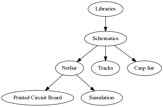
Symbols are added to the schematic from symbol libraries. After the schematic is made, a netlist is generated, which is later used to import the set of connections and footprints into PcbNew.
Symbol placement and editing
Find and place a symbol
To load a symbol into your schematic you can use the icon ![]() . A dialog box allows you to type the name of the symbol to load.
. A dialog box allows you to type the name of the symbol to load.
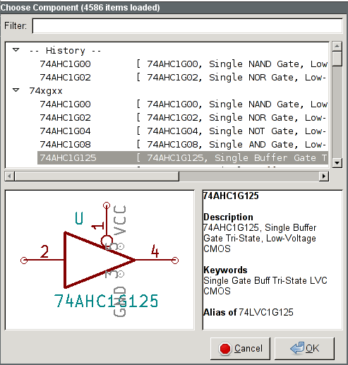
The Choose Symbols dialog will filter symbols by name, keywords, and description according to what you type into the search field. Advanced filters can be used just by typing them:
-
Wildcards: use the characters
?and*respectively to mean "any character" and "any number of characters". -
Relational: if a library part’s description or keywords contain a tag of the format "Key:123", you can match relative to that by typing "Key>123" (greater than), "Key<123" (less than), etc. Numbers may include one of the following case-insensitive suffixes:
p
n
u
m
k
meg
g
t
10-12
10-9
10-6
10-3
103
106
109
1012
ki
mi
gi
ti
210
220
230
240
-
Regular expression: if you’re familiar with regular expressions, these can be used too. The regular expression flavor used is the wxWidgets Advanced Regular Expression style, which is similar to Perl regular expressions.
Before placing the symbol in the schematic, you can rotate it, mirror it, and edit its fields, by either using the hotkeys or the right-click context menu. This can be done the same way after placement.
Here is a symbol during placement:
Puertos de potencia
A power port symbol is a symbol (the symbols are grouped in the “power” library), so they can be placed using the symbol chooser. However, as power placements are frequent, the ![]() tool is available. This tool is similar, except that the search is done directly in the ``power'' library.
tool is available. This tool is similar, except that the search is done directly in the ``power'' library.
Symbol Editing and Modification (already placed component)
There are two ways to edit a symbol:
-
Modification of the symbol itself: position, orientation, unit selection on a multi-unit symbol.
-
Modification of one of the fields of the symbol: reference, value, footprint, etc.
When a symbol has just been placed, you may have to modify its value (particularly for resistors, capacitors, etc.), but it is useless to assign to it a reference number right away, or to select the unit (except for components with locked units, which you have to assign manually). This can be done automatically by the annotation function.
Symbol modification
To modify some feature of a symbol, position the cursor on the symbol, and then either:
-
Double-click on the symbol to open the full editing dialog.
-
Haga clic derecho para abrir el menú contextual y use uno de los comandos: Mover, Orientar, Editar, Borrar, etc,
Modificación de los campos de texto
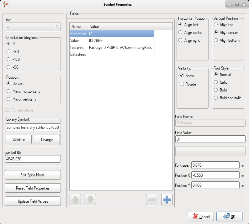
Puede modificar la referencia, valor, posición, orientación, tamaño del texto y visibilidad de los campos:
-
Haga doble clic sobre el campo de texto para modificarlo.
-
Haga clic derecho para abrir el menú contextual y use uno de los comandos: Mover, Rotar, Editar, Borrar, etc.
For more options, or in order to create fields, double-click on the symbol to open the Symbol Properties dialog.
Each field can be visible or hidden, and displayed horizontally or vertically. The displayed position is always indicated for a normally displayed symbol (no rotation or mirroring) and is relative to the anchor point of the symbol.
The option “Reset to Library Defaults” sets the symbol to the original orientation, and resets the options, size and position of each field. However, texts fields are not modified because this could break the schematic.
Hilos, Buses, Etiquetas, Puertos de potencia
Introducción
Todos estos elementos de dibujo pueden ser colocados con las herramientas de la barra de herramientas lateral derecha.
Estos elementos son:
-
Wires: most connections between symbols.
-
Buses: para unir gráficamente etiquetas de bus
-
Polilíneas: para representación gráfica.
-
Uniones: para crear conexiones entre dos hilos o buses que se cruzan.
-
Bus entries: to show connections between wires and buses.
-
Etiquetas: para etiquetar o crear conexiones.
-
Etiquetas globales: para crear conexiones entre hojas.
-
Textos: para comentarios y anotaciones.
-
Marca de "No Conectado": para indicar que un pin no necesita ninguna conexión.
-
Hojas Jerárquicas, y sus pines de conexión.
Conexiones (Hilos y etiquetas)
Existen dos métodos de establecer conexiones:
-
Hilos entre dos pines.
-
Etiquetas.
La siguiente figura muestra los dos métodos:
Nota 1:
El punto de "contacto" de una etiqueta es la esquina inferior izquierda de la primera letra de la etiqueta. Este punto es mostrado mediante un pequeño cuadrado cuando no esta conectado.
Este punto debe estar en contacto con el hilo, o sobreponerse al final de un pin de forma que la etiqueta sea vista como conectada.
Nota 2:
Para establecer una conexión, un segmento de hilo debe estar conectado en su extremo a otro segmento de hilo o a un pin.
Si existe superposición (si un hilo pasa sobre un pin, pero no es conectado al extremo del pin) no existe conexión.
Nota 3:
Los hilos que se cruzan no están implícitamente conectados. Es necesario unirlos mediante un punto de unión si se desea que exista conexión entre ambos.
En la figura previa (los hilos conectados a los pines 22, 21, 20 y 19 del componente DB25FEMALE) muestran el caso de conexión usando el símbolo de unión.
Nota 4:
Si dos etiquetas distintas son colocadas en el mismo hilo, éstas están conectadas entre si y se convierten en equivalentes: todos los elementos conectados a una u otra etiquetas están conectados entre si.
Conexiones (Buses)
En el siguiente esquema, múltiples pines están conectados a buses.
Miembros del Bus
Desde el punto de vista del esquema, un bus es una colección de señales que comienzan con un prefijo común y finalizan con un numero. Por ejemplo, PCA0, PCA1 y PCA2 son miembros del bus PCA.
El bus completo es llamado PCA[N..m] donde N y m son el primer y el ultimo numero de hilo de este bus. Así si PCA tiene 20 miembros desde 0 a 19, el bus completo es nombrado PCA[0..19]. Una colección de señales como PCA0, PCA1, PCA2, WRITE, READ no pueden ser contenidas en un bus
Conexión entre miembros de bus
Los pines conectados mediante el mismo miembro de un bus deben ser conectados mediante etiquetas. No es posible conectar un pin directamente a un bus; este tipo de conexión será ignorado por Eeschema.
En el ejemplo anterior, las conexiones son realizas por las etiquetas colocadas sobre los hilos conectados a los pines. Las entradas de bus (segmentos de hilo a 45 grados) son solo representaciones gráficas, y no forman necesariamente conexiones lógicas.
De hecho, usando el comando repetir (tecla Insertar), las conexiones pueden realizarse rápidamente del siguiente modo, si los pines de los componentes están alineados en orden creciente (caso típico de componentes como memorias, microprocesadores …):
-
Coloque la primera etiqueta (por ejemplo PCA0)
-
Use el comando repetir tanto como sea necesario para colocar el resto de miembros. Eeschema creará automáticamente las siguiente etiquetas (PCA1, PCA2…) alineadas verticalmente, teóricamente sobre la posición de los otros pines.
-
Dibuje el hilo bajo la primera etiqueta. Después utilice el comando repetir para colocar los otros hilos bajo el resto de etiquetas.
-
Si fuera necesario, coloque las entradas al bus del mismo modo (coloque la primera entrada y utilice el comando repetir)
|
En el menú Preferencias/Opciones, puede ajustar los parámetros para las repeticiones.
|
Conexiones globales mediante buses
Puede necesitar conexiones mediante buses, con el fin de conectar dos buses con distinto nombre, o en caso de una jerarquía, para crear conexiones entre hojas diferentes. Puede realizar esta conexiones de la siguiente manera.
Los buses PCA[0..15], ADR[0..7] y BUS[5..10] están conectados juntos (note la unión aquí porque el tramo vertical del bus se une en la mitad del tramo horizontal de bus)
Mas precisamente, los miembros correspondientes están conectados entre si: PCA0 y ADR0 están conectados (así como PCA1 y ADR1 … PCA7 y ADR7)
Además, PCA5, BUS5 y ADR5 estan interconectados (como PCA6, BUS6 y ADR6, y PCA7, BUS7 y ADR7)
PCA8 y BUS8 están también conectados (así como PCA9 y BUS9, y también PCA10 y BUS10)
Conexión de puertos de alimentación
When the power pins of the symbols are visible, they must be connected, as for any other signal.
Symbols such as gates and flip-flops may have invisible power pins. Care must be taken with these because:
-
No puede conectar hilos debido a su invisibilidad.
-
No se conoce sus nombres.
Y además, seria una mala idea hacerlos visibles y conectarlos como los otros pines debido a que el esquema podría volverse ilegible y no estar en concordancia con las convenciones usuales.
|
Si quiere forzar que se muestren estos pines de alimentación invisibles, debe seleccionar la opción ``Mostrar pines de alimentación invisibles'' en el formulario Preferencias/Opciones del menú principal, o el icono |
Eeschema automáticamente conecta los pines de alimentación con el mismo nombre a la red de alimentación con ese nombre. Puede ser necesario unir redes de alimentación con distinto nombre (por ejemplo, "GND" en componentes TTL y "VSS" en componentes MOS); use para esto los puertos de potencia.
No es recomendable usar etiquetas para conexiones de alimentación. Estas solo tienen un alcance de conexión local, y podrían no conectar los pines de alimentación invisibles.
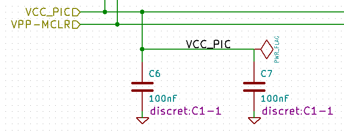
La siguiente figura muestra un ejemplo de conexiones con puertos de potencia.
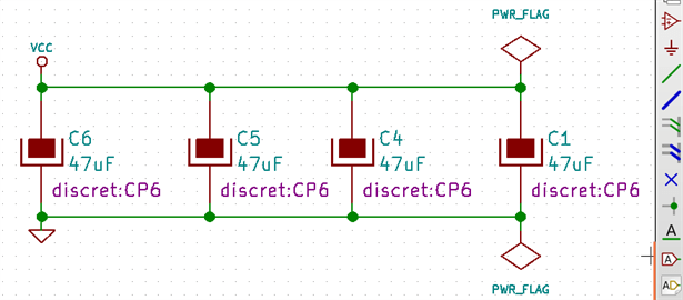
En este ejemplo, la tierra (GND) esta conectada al puerto de potencia VSS, y el puerto de potencia VCC esta conectado a VDD
Dos símbolos PWR_FLAG son visibles. Estos indican que los dos puertos de potencia VCC y GND están realmente conectados a fuentes de alimentación. Sin esos dos símbolos, la herramienta ERC diagnosticaría: Warning: power port not powered.
All these symbols can be found in the ``power'' symbol library.
``No Connect'' flag
These symbols are very useful to avoid undesired ERC warnings. The electrical rules check ensures that no connection has been accidentally left unconnected.
Si los pines realmente deben estar sin conectar, es necesario colocar una marca de "No Conectado" (herramienta ![]() ) sobre esos pines. Estos símbolos no tienen ninguna influencia sobre los netlists generados.
) sobre esos pines. Estos símbolos no tienen ninguna influencia sobre los netlists generados.
Complementos de Dibujo
Comentarios de Texto
It can be useful (to aid in understanding the schematic) to place annotations such as text fields and frames. Text fields (tool ![]() ) and Polyline (tool
) and Polyline (tool ![]() ) are intended for this use, contrary to labels and wires, which are connection elements.
) are intended for this use, contrary to labels and wires, which are connection elements.
Aquí puede encontrar un ejemplo de un cuadro con un comentario en texto.
Bloque de titulo de la hoja
El bloque de titulo de la hoja se edita con la herramienta ![]() .
.
El número de hoja (Hoja X/Y) es actualizado automáticamente.
Rescuing cached symbols
By default, Eeschema loads symbols from the project libraries according to the set paths and library order. This can cause a problem when loading a very old project: if the symbols in the library have changed or have been removed or the library no longer exists since they were used in the project, the ones in the project would be automatically replaced with the new versions. The new versions might not line up correctly or might be oriented differently leading to a broken schematic.
When a project is saved, a cache library with the contents of the current library symbols is saved along with the schematic. This allows the project to be distributed without the full libraries. If you load a project where symbols are present both in its cache and in the system libraries, Eeschema will scan the libraries for conflicts. Any conflicts found will be listed in the following dialog:
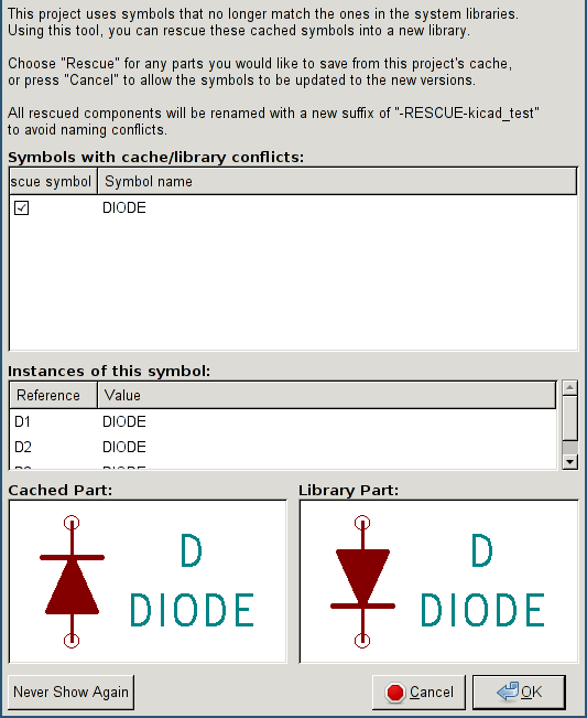
You can see in this example that the project originally used a diode with the cathode facing up, but the library now contains one with the cathode facing down. This change would break the schematic! Pressing OK here will cause the symbol cache library to be saved into a special ``rescue'' library and all the symbols are renamed to avoid naming conflicts.
If you press Cancel, no rescues will be made, so Eeschema will load all the new components by default. If you save the schematic at this point, your cache will be overwritten and the old symbols will not be recoverable. If you have saved the schematic, you can still go back and run the rescue function again by selecting "Rescue Cached Components" in the "Tools" menu to call up the rescue dialog again.
If you would prefer not to see this dialog, you can press "Never Show Again". The default will be to do nothing and allow the new components to be loaded. This option can be changed back in the Libraries preferences.
Esquemas Jerarquicos
Introducción
Una representación jerárquica es generalmente una buena solución para proyectos mas grandes que unas pocas hojas. Si quiere gestionar este tipo de proyectos, sera necesario:
-
Usar hojas grandes, lo que resulta en problemas para imprimir y manejar las hojas.
-
Usar varias hojas, lo que conduce a una estructura jerárquica.
El esquema completo consiste en una hoja principal, llamada hoja raíz, y una serie de hojas hijas que constituyen la jerarquía. Además, una subdivisión adecuada del diseño en hojas separadas, a menudo mejora su legibilidad.
Desde la hoja raíz, debe ser posible encontrar todas las hojas hijas. La gestión de esquemas jerárquicos es bastante fácil con Eeschema, gracias a su "navegador de jerarquía" integrado, accesible mediante el icono ![]() en la barra de herramientas superior
en la barra de herramientas superior
There are two types of hierarchy that can exist simultaneously: the first one has just been evoked and is of general use. The second consists in creating symbols in the library that appear like traditional symbols in the schematic, but which actually correspond to a schematic which describes their internal structure.
Este segundo tipo es usado en el desarrollo de circuitos integrados, pero en este caso tiene que usar bibliotecas de funciones en el esquema que este dibujando.
Eeschema actualmente no soporta este segundo tipo.
Una jerarquía puede ser:
-
simple: una hoja dada es usada solo una vez
-
compleja: una hoja dada es usada mas de una vez (múltiples instancias)
-
plana: que es una jerarquía simple, donde las conexiones entre hojas no son dibujadas.
Eeschema puede tratar con estas tres jerarquías.
La creación de esquemas jerárquicos es fácil, la jerarquía completa es gestionada comenzando desde el esquema raíz, como si solo tuviera un esquema.
Los dos pasos importantes que debe entender son:
-
Como crear una hoja hija.
-
How to build electrical connections between sub-sheets.
Navegando en la Jerarquía
Navigation among sub-sheets is acheived by using the navigator tool accessible via the button ![]() on the top toolbar.
on the top toolbar.
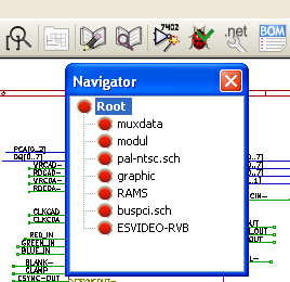
Each sheet is reachable by clicking on its name. For quick access, right click on a sheet name, and choose to Enter Sheet or double click within the bounds of the sheet.
In order to exit the current sheet to the parent sheet, right click anywhere in the schematic where there is no object and select "Leave Sheet" in the context menu or press Alt+Backspace.
Etiquetas locales, jerárquicas y globales
Propiedades
Las etiquetas locales, herramienta ![]() , son señales de conexión solo dentro de una hoja. Las etiquetas jerárquicas (herramienta
, son señales de conexión solo dentro de una hoja. Las etiquetas jerárquicas (herramienta ![]() ) son señales de conexión solo entre una hoja y un pin jerárquico situado en la hoja padre.
) son señales de conexión solo entre una hoja y un pin jerárquico situado en la hoja padre.
Las etiquetas globales (herramienta ![]() ) son señales de conexión a lo largo de toda la jerarquía. Los pines de potencia ( tipos power in y power out) invisibles son como etiquetas globales porque están conectados entre ellos a lo largo de toda la jerarquía.
) son señales de conexión a lo largo de toda la jerarquía. Los pines de potencia ( tipos power in y power out) invisibles son como etiquetas globales porque están conectados entre ellos a lo largo de toda la jerarquía.
| Dentro de una jerarquía (simple o compleja) se pueden usar etiquetas jerárquicas y/o etiquetas globales. |
Summary of hierarchy creation
Tiene que:
-
Colocar en la hoja padre un símbolo de jerarquía llamado "hoja símbolo".
-
Entre dentro del nuevo esquema (hoja hija) con el navegador y dibuje su esquema en ella, como cualquier otro esquema.
-
Draw the electric connections between the two schematics by placing Global Labels (HLabels) in the new schematic (sub-sheet), and labels having the same name in the root sheet, known as SheetLabels. These SheetLabels will be connected to the sheet symbol of the root sheet to the other elements of the schematic like standard symbol pins.
Símbolo de la hoja
Dibuje un rectángulo, definido por dos puntos de su diagonal, que simbolizará la hoja hija.
El tamaño de este rectángulo debe permitirle colocar mas tarde etiquetas particulares, pines de jerarquía, correspondientes a las etiquetas globales (HLabels) en la hoja hija.
These labels are similar to usual symbol pins. Select the tool ![]() .
.
Haga clic para colocar la esquina superior izquierda del rectángulo. Haga clic de nuevo para colocar la esquina inferior derecha, dejando un rectángulo suficientemente grande.
Se le pedirá que escriba el nombre de archivo y en nombre de la hoja para esta hoja hija (con el fin de alcanzar el correspondiente esquema, usando el navegador de jerarquía)
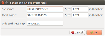
Debe introducir al menos el nombre de archivo. Si no especifica un nombre de hoja, se usará el nombre de fichero como nombre de pagina (modo usual de hacerlo)
Conexion - Pines de Jerarquia
Debe crear aquí los puntos de conexión (pines de jerarquía) para el símbolo que acaba de crear.
These points of connection are similar to normal symbol pins, with however the possibility to connect a complete bus with only one point of connection.
Existen dos maneras de hacer esto.
-
Colocar los distintos pines antes de dibujar la hoja hija (ubicación manual)
-
Colocar los distintos pines tras dibujar la hoja hija, y las etiquetas globales (colocación semi-automática)
Es preferible el empleo de la segunda opción.
Colocación manual:
-
Select the tool
 .
. -
Click on the hierarchy symbol where you want to place the pin.
See below for an example of creating a hierarchical pin named "CONNECTION":
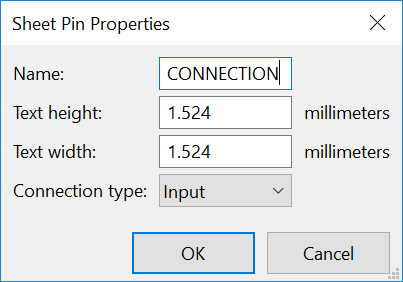
You can define the name, size and direction of the pin during creation or later, by right clicking the pin and selecting Edit Sheet Pin in the popup menu.
Inside the sheet a Hierarchical Label must be preset with the same name as the Hierarchical Pin. Taking care to correctly match these names must be done manually, which is why the second method, below, is preferred.
Colocación Automática:
-
Seleccione la herramienta
 .
. -
Haga clic en el símbolo de jerarquía desde el que quiera importar los pines correspondientes a las etiquetas globales colocadas en el correspondiente esquema. Aparece un pin de jerarquía si existe una etiquetas global, por ej. que no corresponda a un pin ya ubicado.
-
Haga clic donde quiera colocar este pin.
Todos los pines necesarios pueden ser colocados rápidamente y sin error. Su aspecto estará en concordancia con el resto de las etiquetas globales.
Conexiones - Etiquetas de Jerarquía
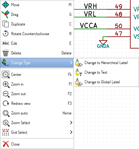
Cada pin del símbolo de hoja recién cread debe corresponder con una etiqueta llamada etiqueta de jerarquía en la hoja hija. Las etiquetas de jerarquía son similares a las etiquetas pero estas proveen conexión entre la hoja hija y la padre. La representación gráfica de las dos etiquetas complementarias (pin y HLabel) es similar. La creación de etiquetas de jerarquía es realizada con la herramienta ![]() .
.
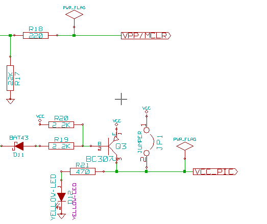
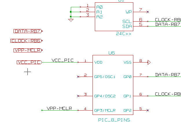
Debajo se muestra un ejemplo de hoja padre:
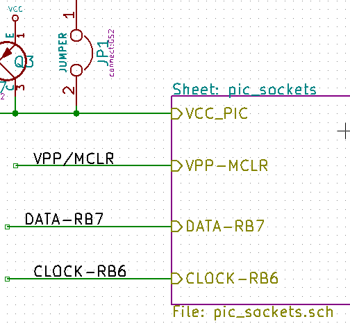
Observe el pin VCC_PIC conectado al conector JP1
Aquí se muestra las conexiones correspondientes en la hoja hija:
Encontramos, de nuevo, las dos correspondientes etiquetas de jerarquía, que proveen la conexión entre las dos hojas jerárquicas.
| Puede usar etiquetas y pines de jerarquía para conectar dos buses, de acuerdo con la sintaxis (Bus[N..m]) anteriormente descrita. |
Etiquetas, etiquetas jerárquicas, etiquetas globales y pines de potencia invisibles
A continuación se indican varios modos de proveer conexión, además de las conexiones mediante hilos.
Etiquetas simples
Las etiquetas simples tienen capacidad de conexión local, limitada a la hoja del esquema donde están ubicadas. Esto es debido a que:
-
Cada hoja tiene un número de hoja.
-
Este número de hoja es asociado a las etiquetas.
Entonces, si coloca la etiqueta "TOTO" en la hoja nº 3, en realidad el verdadero nombre de la etiqueta es "TOTO_3". Si también coloca la etiqueta "TOTO" en la hoja nº 1 (hoja raíz) está colocando una etiqueta llamada "TOTO_1", diferente de "TOTO_3". Esto es siempre cierto, incluso si hay una sola hoja.
Etiquetas de Jerarquia
Todo lo dicho para las etiquetas simples es también cierto para las etiquetas jerárquicas.
Thus in the same sheet, a hierarchical label "TOTO" is considered to be connected to a local label "TOTO", but not connected to a hierarchical label or label called "TOTO" in another sheet.
A hierarchical label is considered to be connected to the corresponding sheet pin symbol in the hierarchical symbol placed in the parent sheet.
Pines de potencia invisibles
It was seen that invisible power pins were connected together if they have the same name. Thus all the power pins declared "Invisible Power Pins" and named VCC are connected all symbol invisible power pins named VCC only within the sheet they are placed.
Esto significa que si coloca una etiqueta VCC en una hoja hija, ésta no estará conectada a los pines VCC ya que la etiqueta es realmente VCC_n, donde n es el numero de hoja.
If you want this label VCC to be really connected to the VCC for the entire schematic, it will have to be explicitly connected to an invisible power pin via a VCC power symbol.
Etiquetas globales
Las etiquetas globales que tienen idéntico nombre están conectadas a lo largo de la jerarquía completa.
(Las etiquetas de potencia como vcc … son etiquetas globales)
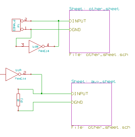
Jerarquías Complejas
Here is an example. The same schematic is used twice (two instances). The two sheets share the same schematic because the file name is the same for the two sheets (``other_sheet.sch''). The sheet names must be unique.
Jerarquías Planas
You can create a project using many sheets without creating connections between these sheets (flat hierarchy) if the following rules are observed:
-
Create a root sheet containing the other sheets which acts as a link between others sheets.
-
No se necesitan conexiones explicitas.
-
Use global labels instead of hierarchical labels in all sheets.
Aquí se muestra un ejemplo de la hoja padre.
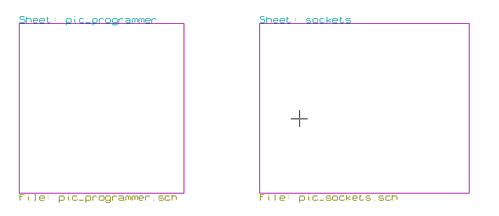
Estas son las dos paginas, conectadas por etiquetas globales.
Esta es la hoja pic_programmer.sch.
Y esta pic_sockets.sch.
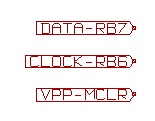
Observe las etiquetas globales.
Symbol Annotation Tool
Introducción
The annotation tool allows you to automatically assign a designator to symbols in your schematic. Annotation of symbols with multiple units will assign a unique suffix to minimize the number of these symbols. The annotation tool is accessible via the icon ![]() . Here you find its main window.
. Here you find its main window.
Available annotation schemes:
-
Annotate all the symbols (reset existing annotation option)
-
Annotate all the symbols, but do not swap any previously annotated multi-unit parts.
-
Annotate only symbols that are currently not annotated. Symbols that are not annotated will have a designator which ends with a '?' character.
-
Anotar toda la arquitectura (use la opción: usar esquema completo)
-
Anotar solo la hoja actual (use la opción: solo página actual)
The ``Reset, but do not swap any annotated multi-unit parts'' option keeps all existing associations between symbols with multilple units. For example, U2A and U2B may be reannotated to U1A and U1B respectively but they will never be reannotated to U1A and U2A, nor to U2B and U2A. This is useful if you want to ensure that pin groupings are maintained.
La elección del orden de anotación determina el método usado para fijar los números de referencias dentro de cada hoja de la arquitectura.
Exceptuando casos particulares, una anotación automática se aplica al proyecto completo (todas las hojas) y a todos los componentes nuevos, si no desea cambiar las anotaciones realizadas previamente.
The Annotation Choice gives the method used to calculate reference:
-
Use first free number in schematic: components are annotated from 1 (for each reference prefix). If a previous annotation exists, only unused numbers will be used.
-
Comenzar por el número de hoja*100 y usar el primer número libre: la anotación comienza por 101 para la hoja 1, 201 para la hoja 2, etc. Si existen mas de 99 elementos con el mismo prefijo (U, R) dentro de la hoja 1, la herramienta de anotado utiliza los números 200 y sucesivos, y el referenciado de la hoja 2 comenzara por el siguiente número libre.
-
Comenzar por el número de hoja*1000 y usar el primer número libre: La anotación comienza por 1001 para la hoja 1, 2001 para la hoja 2.
Algunos ejemplos
Orden de anotación
Este ejemplo muestra 5 elementos ubicados pero no anotados.
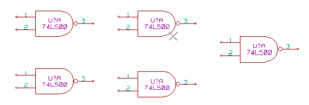
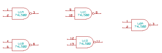
Después de ejecutar la anotación, se obtiene el siguiente resultado.
Ordenar con respecto a la posición X.
Ordenar con respecto a la posición Y.
Puede observarse que cuatro puertas 74LS00 fueron distribuidas en el encapsulado U1, y que la quinta puerta 74LS00 ha sido asignada al siguiente encapsulado, U2.
Preferencias de anotado
Esta es una anotación en la hoja 2 donde fue usada la opción usar primer número libre en el esquema.
La opción comenzar por el número de hoja*100 y usar el primer número libre arrojó el siguiente resultado.
La opción comenzar por el número de hoja*1000 y usar el primer número libre produjo el siguiente resultado.
Verificación del diseño con el Comprobador de Reglas Eléctricas.
Introducción
El Comprobador de Reglas Eléctricas (ERC) realiza un test automático de su esquema. El ERC examina cualquier error en su hoja, como pines no conectados, símbolos de las jerarquías no conectados, salidas cortocircuitadas, etc. Naturalmente, un test automático no es infalible, y el software que hace posible detectar todos los errores de diseño no esta 100% completo. Este test es muy útil, ya que le permite detectar muchos descuidos y pequeños errores.
In fact all detected errors must be checked and then corrected before proceeding as normal. The quality of the ERC is directly related to the care taken in declaring electrical pin properties during symbol library creation. ERC output is reported as errors'' or warnings''.
Como usar el ERC
El ERC puede ser iniciado haciendo clic en el icono ![]() .
.
Los avisos son indicados en los elementos del esquema que generan un error ERC (pines o etiquetas)
|
Puede también borrar marcas de error desde el formulario.
Ejemplo de ERC
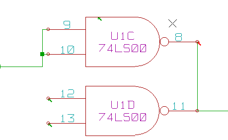
Se pueden observar cuatro errores:
-
Dos salidas han sido erróneamente conectadas juntas (flecha roja)
-
Dos entradas se han dejado sin conectar (flecha verde)
-
Hay un error en un puerto de alimentación invisible, no se encuentra el indicador de alimentación (flecha verde en la parte superior)
Mostrando diagnósticos
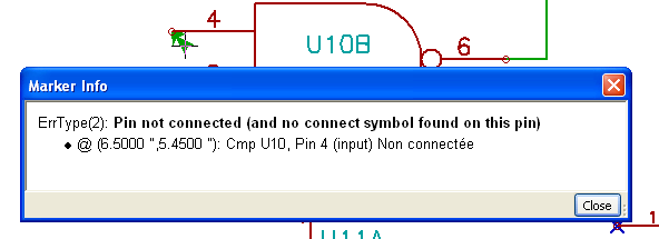
Haciendo clic con el botón derecho sobre una marca se despliega un menú que le permite acceder a la ventana de diagnóstico de marcas ERC.
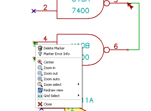
y haciendo clic en "Información de la Marca de Error" puede obtener una descripción del error.
Pines de potencia e indicadores de potencia
Es usual tener un error o aviso en los pines de potencia, aunque todo parezca norma. Mire el ejemplo anterior. Esto sucede porque, en la mayoría de diseños, la alimentación es suministrada mediante conectores que no son fuentes de alimentación (como las salidas de reguladores, que están declaradas como salidas de potencia)
El ERC no detecta ningún pin de salida de potencia alimentando este hilo y lo declara como "no alimentado por una fuente de potencia"
Para evitar este aviso tiene que colocar un "PWR_FLAG" sobre estos puertos de potencia. Eche un vistazo al siguiente ejemplo:
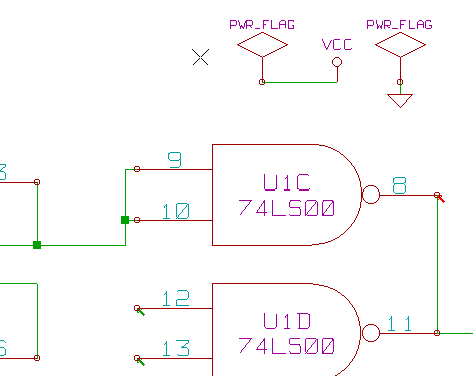
La marca de error ha desaparecido.
Most of the time, a PWR_FLAG must be connected to GND, because regulators have outputs declared as power out, but ground pins are never power out (the normal attribute is power in), so grounds never appear connected to a power source without a power flag symbol.
Configuración
El panel de Opciones le permite configurar las reglas de conectividad que definen las condiciones eléctricas para la detección de errores y avisos.
Las reglas se pueden cambiar haciendo clic sobre el cuadrado oportuno de la matriz, esto alterna su estado cíclicamente entre: normal, aviso, error.
Archivo de reporte ERC
An ERC report file can be generated and saved by checking the option Write ERC report. The file extension for ERC report files is .erc. Here is an example ERC report file.
ERC control (4/1/1997-14:16:4)

***** Sheet 1 (INTERFACE UNIVERSAL)
ERC: Warning Pin input Unconnected @ 8.450, 2.350
ERC: Warning passive Pin Unconnected @ 8.450, 1.950
ERC: Warning: BiDir Pin connected to power Pin (Net 6) @ 10.100, 3.300
ERC: Warning: Power Pin connected to BiDir Pin (Net 6) @ 4.950, 1.400

>> Errors ERC: 4
Creación del Netlist
Resumen
A netlist is a file which describes electrical connections between symbols. These connections are referred to as nets. In the netlist file you can find:
-
The list of the symbols
-
The list of connections (nets) between symbols.
Many different netlist formats exist. Sometimes the symbols list and the list of nets are two separate files. This netlist is fundamental in the use of schematic capture software, because the netlist is the link with other electronic CAD software such as:
-
PCB layout software.
-
Schematic and electrical signal simulators.
-
Compiladores de CPLD (y otros Circuitos Integrados programables).
Eeschema soporta varios formatos de netlist.
-
Formato PCBNEW (circuito impreso).
-
Formato ORCAD PCB2 (circuito impreso)
-
Formato CADSTAR (circuito impreso)
-
Formato Spice, para simuladores Spice (el formato Spice es usado también por otros simuladores).
Formatos de Netlist
Select the tool ![]() to open the netlist creation dialog.
to open the netlist creation dialog.
Seleccione Pcbnew
Seleccione Spice
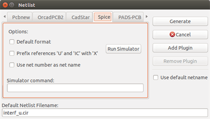
Using the different tabs you can select the desired format. In Spice format you can generate netlists with either net names which makes the SPICE file more human readable or net numbers which are used by older Spice. By clicking the Netlist button, you will be asked for a netlist file name.
| The netlist generation can take up to several minutes for large schematics. |
Ejemplos de Netlist
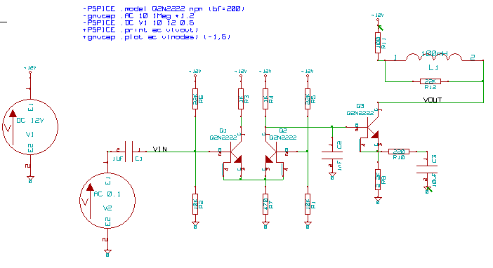
Puede ver debajo un esquema diseñado usando la biblioteca PSPICE:
Ejemplo de un fichero de netlist tipo PCBNEW:
# Eeschema Netlist Version 1.0 generee le 21/1/1997-16:51:15
(
(32E35B76 $noname C2 1NF {Lib=C}
(1 0)
(2 VOUT_1)
)
(32CFC454 $noname V2 AC_0.1 {Lib=VSOURCE}
(1 N-000003)
(2 0)
)
(32CFC413 $noname C1 1UF {Lib=C}
(1 INPUT_1)
(2 N-000003)
)
(32CFC337 $noname V1 DC_12V {Lib=VSOURCE}
(1 +12V)
(2 0)
)
(32CFC293 $noname R2 10K {Lib=R}
(1 INPUT_1)
(2 0)
)
(32CFC288 $noname R6 22K {Lib=R}
(1 +12V)
(2 INPUT_1)
)
(32CFC27F $noname R5 22K {Lib=R}
(1 +12V)
(2 N-000008)
)
(32CFC277 $noname R1 10K {Lib=R}
(1 N-000008)
(2 0)
)
(32CFC25A $noname R7 470 {Lib=R}
(1 EMET_1)
(2 0)
)
(32CFC254 $noname R4 1K {Lib=R}
(1 +12V)
(2 VOUT_1)
)
(32CFC24C $noname R3 1K {Lib=R}
(1 +12V)
(2 N-000006)
)
(32CFC230 $noname Q2 Q2N2222 {Lib=NPN}
(1 VOUT_1)
(2 N-000008)
(3 EMET_1)
)
(32CFC227 $noname Q1 Q2N2222 {Lib=NPN}
(1 N-000006)
(2 INPUT_1)
(3 EMET_1)
)
)
# End
En formato PSPICE, el netlist es como sigue:
* Eeschema Netlist Version 1.1 (Spice format) creation date: 18/6/2008-08:38:03

.model Q2N2222 npn (bf=200)
.AC 10 1Meg \*1.2
.DC V1 10 12 0.5


R12   /VOUT N-000003 22K
R11   +12V N-000003 100
L1   N-000003 /VOUT 100mH
R10   N-000005 N-000004 220
C3   N-000005 0 10uF
C2   N-000009 0 1nF
R8   N-000004 0 2.2K
Q3   /VOUT N-000009 N-000004 N-000004 Q2N2222
V2   N-000008 0 AC 0.1
C1   /VIN N-000008 1UF
V1   +12V 0 DC 12V
R2   /VIN 0 10K
R6   +12V /VIN 22K
R5   +12V N-000012 22K
R1   N-000012 0 10K
R7   N-000007 0 470
R4   +12V N-000009 1K
R3   +12V N-000010 1K
Q2   N-000009 N-000012 N-000007 N-000007 Q2N2222
Q1   N-000010 /VIN N-000007 N-000007 Q2N2222

.print ac v(vout)
.plot ac v(nodes) (-1,5)

.end
Notas en los Netlists
Precauciones en los nombres de los netlist
Many software tools that use netlists do not accept spaces in the component names, pins, nets or other informations. Avoid using spaces in labels, or names and value fields of components or their pins to ensure maximum compatibility.
Del mismo modo, los caracteres especiales distintos de letras y números pueden causar problemas. Note que esta limitación no es relativa a Eeschema sino a los formatos de netlist que pueden resultar intraducibles para otros programas que usen ficheros de netlist.
Netlist PSPICE
Para el simulador Pspice, tiene que incluir algunas lineas de comando en el propio netlist (.PROBE, .AC, etc.).
Cualquier linea de texto incluida en el diagrama de esquema comenzando con la clave -pspice o -gnucap será insertada (sin la clave) al inicio del netlist.
Cualquier linea de texto incluida en el diagrama de esquema comenzando con la clave +pspice o +gnucap será insertada (sin la clave) al inicio del netlist.
Aquí se muestra un ejemplo usando varias textos de una línea y textos multi-línea.
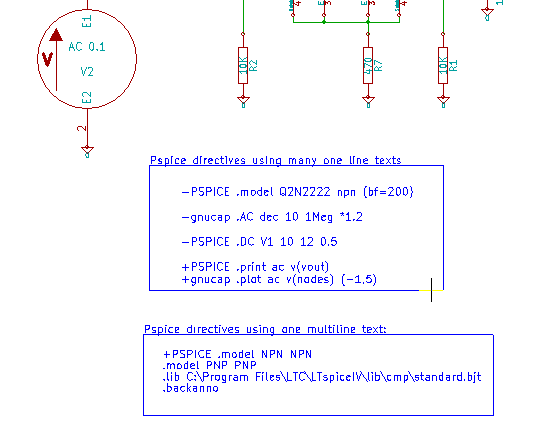
Por ejemplo, si escribe el siguiente texto (¡No use una etiqueta!):
-PSPICE .PROBE
una línea .PROBE se insertará en el netlist.
En el ejemplo anterior tres lineas fueron insertadas al inicio del netlist y dos al final con esta técnica.
Si está usando textos multilinea, las claves +pspice or +gnucap serán necesarias solo una vez:
+PSPICE .model NPN NPN
.model PNP PNP
.lib C:\Program Files\LTC\LTspiceIV\lib\cmp\standard.bjt
.backanno
Crea las siguientes cuatro lineas:
.model NPN NPN
.model PNP PNP
.lib C:\Program Files\LTC\LTspiceIV\lib\cmp\standard.bjt
.backanno
Also note that the GND net must be named 0 (zero) for Pspice.
Otros Formatos
Para otros formatos de netlist puede añadir conversores de netlist en forma de plugins. Estos conversores son automáticamente lanzados por Eeschema. El capítulo 14 muestra algunas explicaciones y ejemplos de conversores.
Un conversor es un fichero de texto (en formato xls) pero puede usarse otros lenguajes como Python. Cuando se usa el formato xls, una herramienta (xsltproc.exe o xsltproc) lee el fichero intermedio creado por Eeschema, y el archivo conversor crea el fichero de salida. En este caso, el fichero conversor (una hoja de estilo) es muy pequeño y fácil de escribir.
Inicie la ventana de diálogo
Puede añadir un nuevo plugin de netlist mediante el botón Añadir Plugin.
Aquí se muestra la ventana de ajuste del plugin PadsPcb:
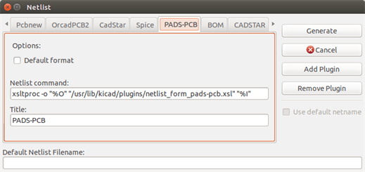
La configuración requerirá:
-
Un título (por ejemplo, el nombre del formato de netlist)
-
El plug-in a lanzar.
Cuando el netlist es generado:
-
Eeschema crea un fichero intermedio *.tmp, por ejemplo test.tmp.
-
Eeschema ejecuta el plug-in, que lee test.tmp y crea test.net.
Formato de Linea de Comando
Aquí se muestra un ejemplo usando xsltproc.exe como herramienta para convertir archivos .xsl, y un archivo metlist_from_pads-pcb.xsl como hoja de estilo conversora:
f:/kicad/bin/xsltproc.exe -o %O.net f:/kicad/bin/plugins/netlist_form_pads-pcb.xsl %I
Con:
| f:/kicad/bin/xsltproc.exe | A tool to read and convert xsl file |
|---|---|
-o %O.net |
Output file: %O will define the output file. |
f:/kicad/bin/plugins/netlist_form_pads-pcb.xsl |
File name converter (a sheet style, xsl format). |
%I |
Will be replaced by the intermediate file created by Eeschema (*.tmp). |
Para un fichero de esquema llamado test.sch, la linea de comando actual es:
f:/kicad/bin/xsltproc.exe -o test.net f:/kicad/bin/plugins/netlist_form_pads-pcb.xsl test.tmp.
Conversor y Hoja de Estilo (plug-in)
Este es un software muy simple porque su propósito es simplemente convertir un fichero de entrada (el fichero de texto intermedio) a otro fichero de texto. Además, desde el fichero de texto intermedio, se puede crear una lista de materiales (BOM).
Cuando se usa xsltproc como herramienta de conversión solo será generado el fichero tipo hoja.
Formatos de fichero netlist intermedios
Vea el capitulo 14 para mas explicaciones sobre xslproc, descripciones del formato de archivo intermedio, y algunos ejemplo de conversores de estilo hoja.
Plot e Imprimir
Introducción
Puede acceder a ambos comandos mediante del menú archivo.
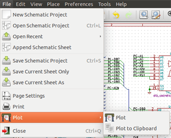
Los formatos de salida soportados son Postscript, PDF, SVG, DXF and HPGL. Puede además imprimir directamente a su impresora.
Comandos comunes de impresión
- Imprimir página actual
-
Imprime un fichero solo para la página actual.
- Imprimir todas las páginas
-
Le permite imprimir la jerarquía completa (se genera un fichero para cada hoja)
Imprimir en Postscript
Este comando le permite crear archivos PostScript.

El nombre del archivo es el nombre de la hoja con la extensión .ps. Puede deshabilitar la opción "Plot border and title block". Esto es útil si quiere crear un fichero postscript para encapsular (formato .eps) un diagrama en un software de procesamiento de texto. La ventana de mensaje muestra el nombre de archivo creado.
Imprimir en PDF
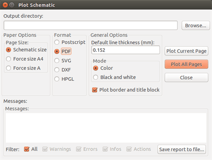
Le permite crear fichero de impresión usando el formato PDF. El nombre del archivo es el nombre de la hoja con la extensión .pdf.
Imprimir en SVG
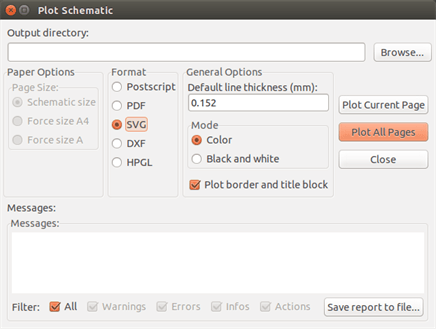
Le permite crear fichero de impresión usando el formato vectorial SVG. El nombre del fichero es el nombre de la hoja con la extensión .svg.
Imprimir en DXF
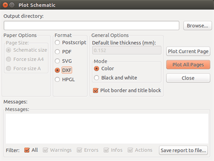
Le permite crear un fichero de impresión usando el formato DXF. El nombre del fichero es el nombre de la hoja con extensión .dxf.
Imprimir en HPGL
Este comando le permite crear un fichero HPGL. En este formato puede definir:
-
Tamaño de la página.
-
Origen.
-
Ancho de las lineas (en mm).
La ventana de ajustes de ploteado es la siguiente:
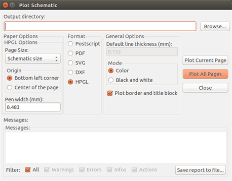
El nombre del fichero de salida será el nombre de la hoja con extensión .plt.
Selección del tamaño de la hoja
Normalmente el tamaño de la hoja es comprobado. En este caso, se usará el tamaño de hoja definido en el menú del bloque y la escala elegida será 1. Si se selecciona un tamaño de hoja diferente (A4 con A0, o A con E), la escala se ajusta automáticamente al tamaño de la hoja.
Ajuste de offset
Para todas las dimensiones estándar, puede ajustar el offset para centrar el dibujo tan precisamente como sea posible. Dado que los plotters tienen el punto de origen en el centro o en la esquina inferior izquierda, es necesario que sea posible introducir un offset para imprimir adecuadamente.
Generalidades:
-
Para plotters que tengan su punto de origen en el centro de la hoja el offset debe ser negativo y ajustarse a la mitad de las dimensiones de la hoja.
-
Para plotters que tengan su punto de origen en la esquina inferior izquierda el offset debe ser ajustado a 0.
Ajustar el offset:
-
Seleccionar el tamaño de la hoja.
-
Ajustar el offset en X y el offset en Y.
-
Pulsar en aceptar offset.
Imprimir en papel
Este comando, disponible a través del icono ![]() , permite visualizar y generar ficheros para impresoras estándar.
, permite visualizar y generar ficheros para impresoras estándar.
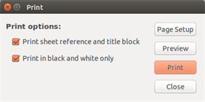
La opción "Imprimir referencia de hoja y bloque de titulo" habilita o deshabilita las referencias de la hoja y el bloque de titulo.
La opción "Imprimir en blanco y negro" ajusta la impresión monocromo. Esta opción normalmente es necesaria si se usa una impresora láser en blanco y negro, ya que los colores son impresos en tonos medios que normalmente no son tan legibles.
Symbol Library Editor
General Information About Symbol Libraries
A symbol is a schematic element which contains a graphical representation, electrical connections, and fields defining the symbol. Symbols used in a schematic are stored in symbol libraries. Eeschema provides a symbol library editing tool that allows you to create libraries, add, delete or transfer symbols between libraries, export symbols to files, and import symbols from files. The library editing tool provides a simple way to manage symbol library files.
Symbol Library Overview
A symbol library is composed of one or more symbols. Generally the symbols are logically grouped by function, type, and/or manufacturer.
A symbol is composed of:
-
Elementos gráficos (lineas, círculos, arcos, texto etc) que proveen la definición del símbolo.
-
Pins que proveen tanto propiedades gráficas (líneas, reloj, invertidas, activo a nivel bajo, etc) como eléctricas (entrada, salida, bidireccional, etc) usadas en la herramienta de Comprobación de Reglas Eléctricas (ERC)
-
Campos como referencias, valores, huella correspondiente para el diseño del PCB, etc.
-
Aliases used to associate a common symbol such as a 7400 with all of its derivatives such as 74LS00, 74HC00, and 7437. All of these aliases share the same library symbol.
Proper symbol designing requires:
-
Defining if the symbol is made up of one or more units.
-
Defining if the symbol has an alternate body style also known as a De Morgan representation.
-
Diseñar su representación simbólica usando líneas, rectángulos, círculos, polígonos y texto.
-
Añadir terminales definiendo cuidadosamente cada representación gráfica, su nombre, número y propiedades eléctricas (entrada, salida, tri-estado, alimentación, etc).
-
Adding an alias if other symbols have the same design and pin out or removing one if the symbol has been created from another symbol.
-
Añadir campos opcionales como nombre de la huella usada por el programa de diseño de PCB y/o definiendo su visibilidad.
-
Documenting the symbol by adding a description string and links to data sheets, etc.
-
Salvar el componente en la biblioteca deseada.
Symbol Library Editor Overview
The symbol library editor main window is shown below. It consists of three tool bars for quick access to common features and a symbol viewing/editing area. Not all commands are available on the tool bars but can be accessed using the menus.
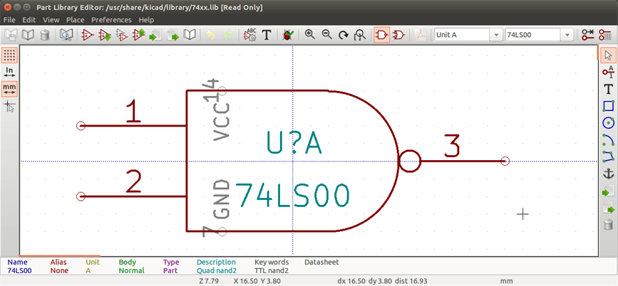
Barra de herramientas principal
The main tool bar typically located at the top of the main window shown below consists of the library management tools, undo/redo commands, zoom commands, and symbol properties dialogs.

|
Save the currently selected library. The button will be disabled if no library is currently selected or no changes to the currently selected library have been made. |
|
Select the library to edit. |
|
Delete a symbol from the currently selected library or any library defined by the project if no library is currently selected. |
|
Open the symbol library browser to select the library and symbol to edit. |
|
Create a new symbol. |
|
Load symbol from currently selected library for editing. |
|
Create a new symbol from the currently loaded symbol. |
|
Save the current symbol changes in memory. The library file is not changed. |
|
Import one symbol from a file. |
|
Export the current symbol to a file. |
|
Create a new library file containing the current symbol. Note: new libraries are not automatically added to the project. |
|
Undo last edit. |
|
Redo last undo. |
|
Edit the current symbol properties. |
|
Edit the fields of current symbol. |
|
Test the current symbol for design errors. |
|
Zoom in. |
|
Zoom out. |
|
Refresh display. |
|
Zoom to fit symbol in display. |
|
Select the normal body style. The button is disabled if the current symbol does not have an alternate body style. |
|
Select the alternate body style. The button is disabled if the current symbol does not have an alternate body style. |
|
Show the associated documentation. The button will be disabled if no documentation is defined for the current symbol. |
|
Select the unit to display. The drop down control will be disabled if the current symbol is not derived from multiple units. |
|
Select the alias. The drop down control will be disabled if the current symbol does not have any aliases. |
|
Pin editing: independent editing for pin shape and position for symbols with multiple units and alternate symbols. |
|
Show pin table. |
Barra de herramientas de elementos
The vertical toolbar typically located on the right hand side of the main window allows you to place all of the elements required to design a symbol. The table below defines each toolbar button.
|
Select tool. Right-clicking with the select tool opens the context menu for the object under the cursor. Left-clicking with the select tool displays the attributes of the object under the cursor in the message panel at the bottom of the main window. Double-left-clicking with the select tool will open the properties dialog for the object under the cursor. |
|
Pin tool. Left-click to add a new pin. |
|
Graphical text tool. Left-click to add a new graphical text item. |
|
Rectangle tool. Left-click to begin drawing the first corner of a graphical rectangle. Left-click again to place the opposite corner of the rectangle. |
|
Circle tool. Left-click to begin drawing a new graphical circle from the center. Left-click again to define the radius of the circle. |
|
Arc tool. Left-click to begin drawing a new graphical arc item from the center. Left-click again to define the first arc end point. Left-click again to define the second arc end point. |
|
Polygon tool. Left-click to begin drawing a new graphical polygon item in the current symbol. Left-click for each addition polygon line. Double-left-click to complete the polygon. |
|
Anchor tool. Left-click to set the anchor position of the symbol. |
|
Import a symbol from a file. |
|
Export the current symbol to a file. |
|
Delete tool. Left-click to delete an object from the current symbol. |
Barra de herramientas Opciones
La barra de herramientas que se ubica generalmente a la izquierda de la pantalla principal le permite ajustar algunas de las opciones del editor de componentes. La siguiente tabla define cada botón de la barra de herramientas.
|
Toggle grid visibility on and off. |
|
Set units to inches. |
|
Set units to millimeters. |
|
Toggle full screen cursor on and off. |
Selección y mantenimiento de bibliotecas
The selection of the current library is possible via the ![]() which shows you all available libraries and allows you to select one. When a symbol is loaded or saved, it will be put in this library. The library name of symbol is the contents of its value field.
which shows you all available libraries and allows you to select one. When a symbol is loaded or saved, it will be put in this library. The library name of symbol is the contents of its value field.
|
Select and Save a Symbol
When you edit a symbol you are not really working on the symbol in its library but on a copy of it in the computer’s memory. Any edit action can be undone easily. A symbol may be loaded from a local library or from an existing symbol.
Symbol Selection
Clicking the ![]() on the main tool bar displays the list of the available symbols that you can select and load from the currently selected library.
on the main tool bar displays the list of the available symbols that you can select and load from the currently selected library.
If a symbol is selected by its alias, the name of the loaded symbol is displayed on the window title bar instead of the selected alias. The list of symbol aliases is always loaded with each symbol and can be edited. You can create a new symbol by selecting an alias of the current symbol from the  . The first item in the alias list is the root name of the symbol. . The first item in the alias list is the root name of the symbol.
|
|
Alternatively, clicking the |
Save a Symbol
After modification, a symbol can be saved in the current library, in a new library, or exported to a backup file.
To save the modified symbol in the current library, click the ![]() . Please note that the update command only saves the symbol changes in the local memory. This way, you can make up your mind before you save the library.
. Please note that the update command only saves the symbol changes in the local memory. This way, you can make up your mind before you save the library.
To permanently save the symbol changes to the library file, click the ![]() which will overwrite the existing library file with the symbol changes.
which will overwrite the existing library file with the symbol changes.
If you want to create a new library containing the current symbol, click the ![]() . You will be asked to enter a new library name.
. You will be asked to enter a new library name.
|
Las bibliotecas recién creadas no son automáticamente añadidas al proyecto actual. You must add any new library you wish to use in a schematic to the list of project libraries in Eeschema using the Symbol Library Table dialog. |
Click the ![]() to create a file containing only the current symbol. This file will be a standard library file which will contain only one symbol. This file can be used to import the symbol into another library. In fact, the create new library command and the export command are basically identical.
to create a file containing only the current symbol. This file will be a standard library file which will contain only one symbol. This file can be used to import the symbol into another library. In fact, the create new library command and the export command are basically identical.
Transfer Symbols to Another Library
You can very easily copy a symbol from a source library into a destination library using the following commands:
-
Seleccione la biblioteca origen pulsando en
 .
. -
Load the symbol to be transferred by clicking the
 . The symbol will be displayed in the editing area.
 -
Seleccione la biblioteca de destino haciendo clic en
. -
Save the current symbol to the new library in the local memory by clicking the
 .
. -
Save the symbol in the current local library file by clicking the
 .
.
Discarding Symbol Changes
When you are working on a symbol, the edited symbol is only a working copy of the actual symbol in its library. This means that as long as you have not saved it, you can just reload it to discard all changes made. If you have already updated it in the local memory and you have not saved it to the library file, you can always quit and start again. Eeschema will undo all the changes.
Creating Library Symbols
Create a New Symbol
A new symbol can be created by clicking the ![]() . You will be asked for a symbol name (this name is used as default value for the value field in the schematic editor), the reference designator (U, IC, R…), the number of units per package (for example a 7400 is made of 4 units per package) and if an alternate body style (sometimes referred to as DeMorgan) is desired. If the reference designator field is left empty, it will default to "U". These properties can be changed later, but it is preferable to set them correctly at the creation of the symbol.
. You will be asked for a symbol name (this name is used as default value for the value field in the schematic editor), the reference designator (U, IC, R…), the number of units per package (for example a 7400 is made of 4 units per package) and if an alternate body style (sometimes referred to as DeMorgan) is desired. If the reference designator field is left empty, it will default to "U". These properties can be changed later, but it is preferable to set them correctly at the creation of the symbol.
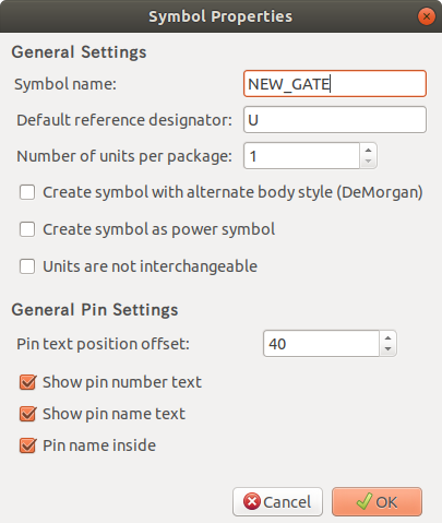
A new symbol will be created using the properties above and will appear in the editor as shown below.
Create a Symbol from Another Symbol
Often, the symbol that you want to make is similar to one already in a symbol library. In this case it is easy to load and modify an existing symbol.
-
Load the symbol which will be used as a starting point.
-
Click on the
 or modify its name by right-clicking on the value field and editing the text. If you chose to duplicate the current symbol, you will be prompted for a new symbol name.
 -
If the model symbol has aliases, you will be prompted to remove aliases from the new symbol which conflict with the current library. If the answer is no the new symbol creation will be aborted. Symbol libraries cannot have any duplicate names or aliases.
-
Edit the new symbol as required.
-
Update the new symbol in the current library by clicking the
or save to a new library by clicking the  or if you want to save this new symbol in an other existing library select the other library by clicking on the and save the new symbol.
 -
Guarde el fichero de la biblioteca actual al disco haciendo clic
.
Symbol Properties
Symbol properties should be carefully set during the symbol creation or alternatively they are inherited from the copied symbol. To change the symbol properties, click on the ![]() to show the dialog below.
to show the dialog below.
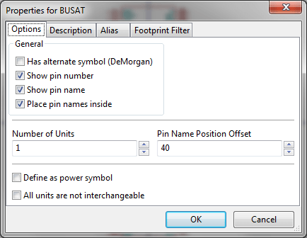
It is very important to correctly set the number of units per package and the alternate symbolic representation, if enabled, because when pins are edited or created the corresponding pins for each unit will be affected. If you change the number of units per package after pin creation and editing, there will be additional work to add the new unit pins and symbols. Nevertheless, it is possible to modify these properties at any time.
The graphic options "Show pin number" and "Show pin name" define the visibility of the pin number and pin name text. This text will be visible if the corresponding options are checked. The option "Place pin names inside" defines the pin name position relative to the pin body. This text will be displayed inside the symbol outline if the option is checked. In this case the "Pin Name Position Offset" property defines the shift of the text away from the body end of the pin. A value from 30 to 40 (in 1/1000 inch) is reasonable.
The example below shows a symbol with the "Place pin name inside" option unchecked. Notice the position of the names and pin numbers.
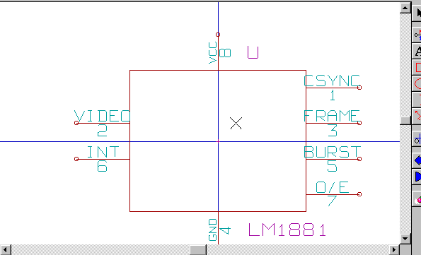
Symbols with Alternate Symbolic Representation
If the symbol has more than one symbolic repersentation, you will have to select one representation to edit them. To edit the normal representation, click the ![]() .
.
To edit the alternate representation, click on the ![]() . Use the shown below to select the unit you wish to edit.
. Use the shown below to select the unit you wish to edit.
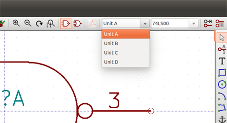
Elementos gráficos
Graphical elements create the representation of a symbol and contain no electrical connection information. Their design is possible using the following tools:
-
Líneas y polígonos definidos mediante sus puntos iniciales y finales.
-
Rectángulos definidos mediante dos esquinas opuestas.
-
Círculos definidos mediante su centro y radio.
-
Arcos definidos mediante sus puntos inicial y final asi como el centro de la circunferencia que lo contiene. Un arco va desde 0º a 180º.
The vertical toolbar on the right hand side of the main window allows you to place all of the graphical elements required to design the representation of a symbol.
Características de los elementos gráficos
Cada elemento gráfico (línea, arco, círculo, etc.) puede definirse como común a todas las unidades y/o estilos de símbolo, o específicos a una unidad o estilo de símbolo concreto. Puede accederse rápidamente a las opciones de los elementos mediante un menú contextual haciendo clic derecho en el elemento. Debajo se muestra el menú contextual para un elemento línea.
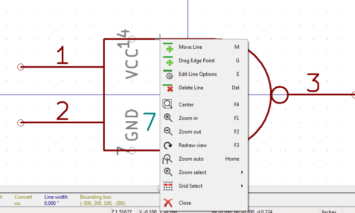
Además puede realizar doble clic sobre un elemento para modificar sus propiedades. Debajo se muestra el formulario de propiedades para un elemento polígono.
Las propiedades de un elemento gráfico son:
-
Ancho de línea que define el ancho de las líneas del elemento expresadas en las unidades de dibujo actuales
-
The "Common to all units in symbol" setting defines if the graphical element is drawn for each unit in symbol with more than one unit per package or if the graphical element is only drawn for the current unit.
-
The "Common by all body styles (DeMorgan)" setting defines if the graphical element is drawn for each symbolic representation in symbols with an alternate body style or if the graphical element is only drawn for the current body style.
-
El ajuste de estilo de relleno determina si el símbolo definido por el elemento gráfico se mostrara sin relleno, con el fondo relleno, o con el primer plano relleno.
Elementos de texto
The ![]() allows for the creation of graphical text. Graphical text is always readable, even when the symbol is mirrored. Please note that graphical text items are not fields.
allows for the creation of graphical text. Graphical text is always readable, even when the symbol is mirrored. Please note that graphical text items are not fields.
Multiple Units per Symbol and Alternate Body Styles
Symbols can have two symbolic representations (a standard symbol and an alternate symbol often referred to as "DeMorgan") and/or have more than one unit per package (logic gates for example). Some symbols can have more than one unit per package each with different symbols and pin configurations.
Consider for instance a relay with two switches which can be designed as a symbol with three different units: a coil, switch 1, and switch 2. Designing a symbol with multiple units per package and/or alternate body styles is very flexible. A pin or a body symbol item can be common to all units or specific to a given unit or they can be common to both symbolic representation so are specific to a given symbol representation.
Por defecto, los pines son específicos a la representación simbólica de cada unidad, debido a que el número del pin es especifico cada unidad, y la forma depende de la representación simbólica. Cuando un pin es común para cada unidad o cada representación simbólica, este debe ser creado solo una vez para todas las unidades o representaciones simbólicas (este es el caso de los pines de alimentación). Este es también el caso del contorno y textos que son comunes para todas las unidades (aunque normalmente son específicos para cada representación simbólica)
Example of a Symbol Having Multiple Units with Different Symbols:
Este es un ejemplo de un relé definido por tres unidades por encapsulado, contacto 1, contacto 2 y la bobina:
Opción: Los pines no están enlazados. Se pueden añadir o editar pines para cada unidad sin que interfiera en los pines de las otras unidades.
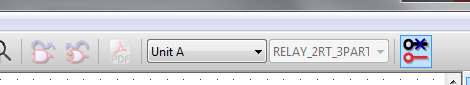
Debe seleccionarse la opción "Todas las unidades no son intercambiables".
Unidad 1
Unidad 2
Unidad 3
Esta no tiene el mismo símbolo ni distribución de pines que las unidades 1 y 2, y por tanto no es intercambiable con ellas.
Elementos Gráficos Simbólicos
Shown below are properties for a graphic body element. From the relay example above, the three units have different symbolic representations. Therefore, each unit was created separately and the graphical body elements must have the "Common to all units in symbol" disabled.
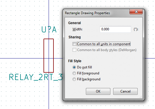
Edición y Creación de Pines
Puede hacer clic en ![]() para crear e insertar un pin. La edición de todas las características del pin se realiza mediante doble clic en el pin o clic derecho para abrir el menú contextual del mismo. Los pines deben ser creados con cuidado porque cualquier error tendrá consecuencias en el diseño del PCB. Cualquier pin que sea colocado en el componente puede ser editado, borrado y/o movido.
para crear e insertar un pin. La edición de todas las características del pin se realiza mediante doble clic en el pin o clic derecho para abrir el menú contextual del mismo. Los pines deben ser creados con cuidado porque cualquier error tendrá consecuencias en el diseño del PCB. Cualquier pin que sea colocado en el componente puede ser editado, borrado y/o movido.
Resumen de Pines
Un pin es definido por su representación gráfica, su nombre y su "número". El "número" del pin es definido por un conjunto de 4 letras y/o números. Para que la herramienta de Comprobación de Reglas Eléctricas (ERC) sea útil, el tipo "eléctrico" del pin (entrada, salida, tri-estado) también debe ser definido correctamente. Si no se define este tipo correctamente, la comprobación eléctrica del esquema puede ser invalida.
Notas importantes:
-
No use espacio en los campos nombre y número del pin.
-
Para definir un nombre de pin como señal invertida (sobre-rayada) use el carácter
~. El siguiente carácter~finalizará el sobre-rayado. Por ejemplo~FO~Omostrará FO O. -
Si el nombre del pin se reduce a un único símbolo
~, el pin se considera como no nombrado. -
Los nombres de pin que comienzan por
#son reservados para los puertos de alimentación. -
Un "número" de pin consiste en 1 a 4 letras y/o números. 1,2,..9999 son números validos. A1, B3, Anod, Gnd, Wire, etc también son válidos.
-
Duplicate pin "numbers" cannot exist in a symbol.
Propiedades de Pin
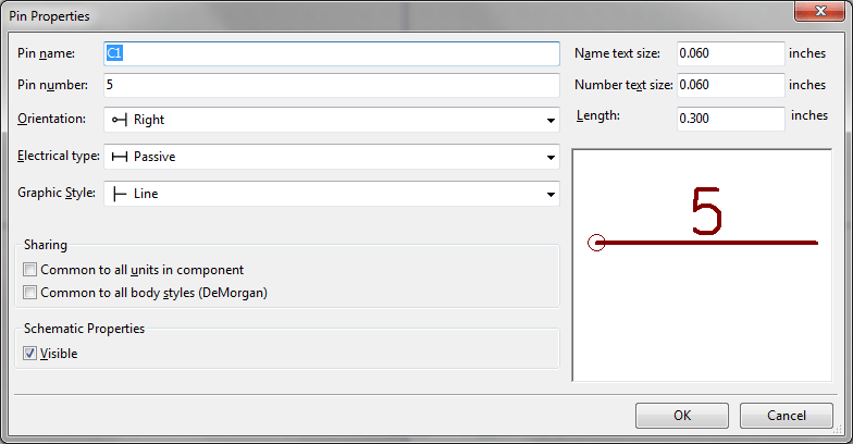
El formulario de propiedades del pin le permite editar todas las características de un pin. Este formulario aparece automáticamente cuando crea un pin o cuando hace doble clic en un pin que ya exista. Desde este formulario podrá modificar:
-
Nombre y tamaño del texto del nombre.
-
Número y tamaño del texto del número.
-
Longitud.
-
Tipo eléctrico y representación gráfica.
-
Si el pin está definido para todos las unidades y símbolos alternativos.
-
Visibilidad.
Estilo gráfico del pin.
En la siguiente figura se muestran los diferentes estilos gráficos de los pines. La elección de un estilo gráfico no tiene ninguna influencia en el tipo eléctrico del mismo.
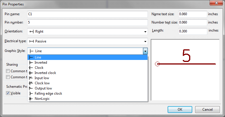
Tipos Eléctricos de Pin
Elegir el tipo eléctrico correctamente es muy importante para la herramienta de comprobación ERC. Los tipos eléctricos definidos son:
-
Bidireccional, que indica un pin bidireccional conmutable entre entrada y salida (por ejemplo el bus de datos de un microprocesador)
-
Tri-estado es la típica salida con 3 estados (alta impedancia)
-
Passive is used for passive symbol pins, resistors, connectors, etc.
-
No especificado puede ser usado cuando no es importante para el test ERC.
-
Power input is used for the symbol’s power pins. Power pins are automatically connected to the other power input pins with the same name.
-
Pines de salida de potencia son usados para salidas de reguladores.
-
Emisor abierto y Colector abierto son usados para salidas lógicas definidas como tales en sus componentes.
-
Not connected is used when a symbol has a pin that has no internal connection.
Propiedades Globales del Pin.
You can modify the length or text size of the name and/or number of all the pins using the Global command entry of the pin context menu. Click on the parameter you want to modify and type the new value which will then be applied to all of the current symbol’s pins.
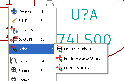
Definición de pines para múltiples unidades y representaciones de símbolo alternativas
Symbols with multiple units and/or graphical representations are particularly problematic when creating and editing pins. The majority of pins are specific to each unit (because their pin number is specific to each unit) and to each symbolic representation (because their form and position is specific to each symbolic representation). The creation and the editing of pins can be problematic for symbols with multiple units per package and alternate symbolic representations. The symbol library editor allows the simultaneous creation of pins. By default, changes made to a pin are made for all units of a multiple unit symbol and both representations for symbols with an alternate symbolic representation.
La única excepción a esto son los campos tipo gráfico y nombre del pin. Esa dependencia fue establecida para permitir una creación y edición de pines mas fácil en la mayoría de los casos. Esta dependencia puede ser deshabilitada cambiando el estado de ![]() en la barra de herramientas principal. Esto le permitirá crear pines para cada unidad y representación completamente independientes.
en la barra de herramientas principal. Esto le permitirá crear pines para cada unidad y representación completamente independientes.
A symbol can have two symbolic representations (representation known as``DeMorgan'') and can be made up of more than one unit as in the case of symbols with logic gates. For certain symbols, you may want several different graphic elements and pins. Like the relay sample shown in the previous section, a relay can be represented by three distinct units: a coil, switch contact 1, and switch contact 2.
The management of the symbols with multiple units and symbols with alternate symbolic representations is flexible. A pin can be common or specific to different units. A pin can also be common to both symbolic representations or specific to each symbolic representation.
Por defecto, los pines son específicos de cada unidad, dado que sus números son diferentes para cada unidad, y su diseño es diferente para cada representación simbólica. Cuando un pin es común para todas las unidades este solo se dibuja una vez como en el caso de los pines de alimentación.
An example is the output pin 7400 quad dual input NAND gate. Since there are four units and two symbolic representations, there are eight separate output pins defined in the symbol definition. When creating a new 7400 symbol, unit A of the normal symbolic representation will be shown in the library editor. To edit the pin style in alternate symbolic representation, it must first be enabled by clicking the ![]() button on the tool bar. To edit the pin number for each unit, select the appropriate unit using the drop down control.
button on the tool bar. To edit the pin number for each unit, select the appropriate unit using the drop down control.
Symbol Fields
All library symbols are defined with four default fields. The reference designator, value, footprint assignment, and documentation file link fields are created whenever a symbol is created or copied. Only the reference designator and value fields are required. For existing fields, you can use the context menu commands by right-clicking on the pin. Symbols defined in libraries are typically defined with these four default fields. Additional fields such as vendor, part number, unit cost, etc. can be added to library symbols but generally this is done in the schematic editor so the additional fields can be applied to all of the symbols in the schematic.
Editing Symbol Fields
To edit an existing symbol field, right-click on the field text to show the field context menu shown below.
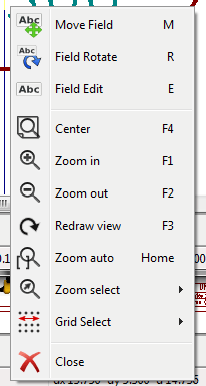
To edit undefined fields, add new fields, or delete optional fields ![]() on the main tool bar to open the field properties dialog shown below.
on the main tool bar to open the field properties dialog shown below.
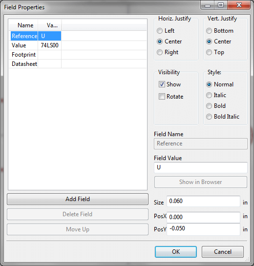
Fields are text sections associated with the symbol. Do not confuse them with the text belonging to the graphic representation of this symbol.
Notas importantes:
-
Modifying value fields effectively creates a new symbol using the current symbol as the starting point for the new symbol. This new symbol has the name contained in the value field when you save it to the currently selected library.
-
The field edit dialog above must be used to edit a field that is empty or has the invisible attribute enabled.
-
La huella es definida como una huella absoluta usando la notación LIBNAME:FPNAME donde LIBNAME es el nombre de la biblioteca de símbolos definido en la tabla de bibliotecas de símbolos (Ver la sección "Tabla de Bibliotecas de Símbolos" en el "Manual de Referencia" de Pcbnew) y FPNAME es el nombre de la huella en la biblioteca LIBNAME
Símbolos de Potencia
Power symbols are created the same way as normal symbols. It may be useful to place them in a dedicated library such as power.lib. Power symbols consist of a graphical symbol and a pin of the type "Power Invisible". Power port symbols are handled like any other symbol by the schematic capture software. Some precautions are essential. Below is an example of a power +5V symbol.
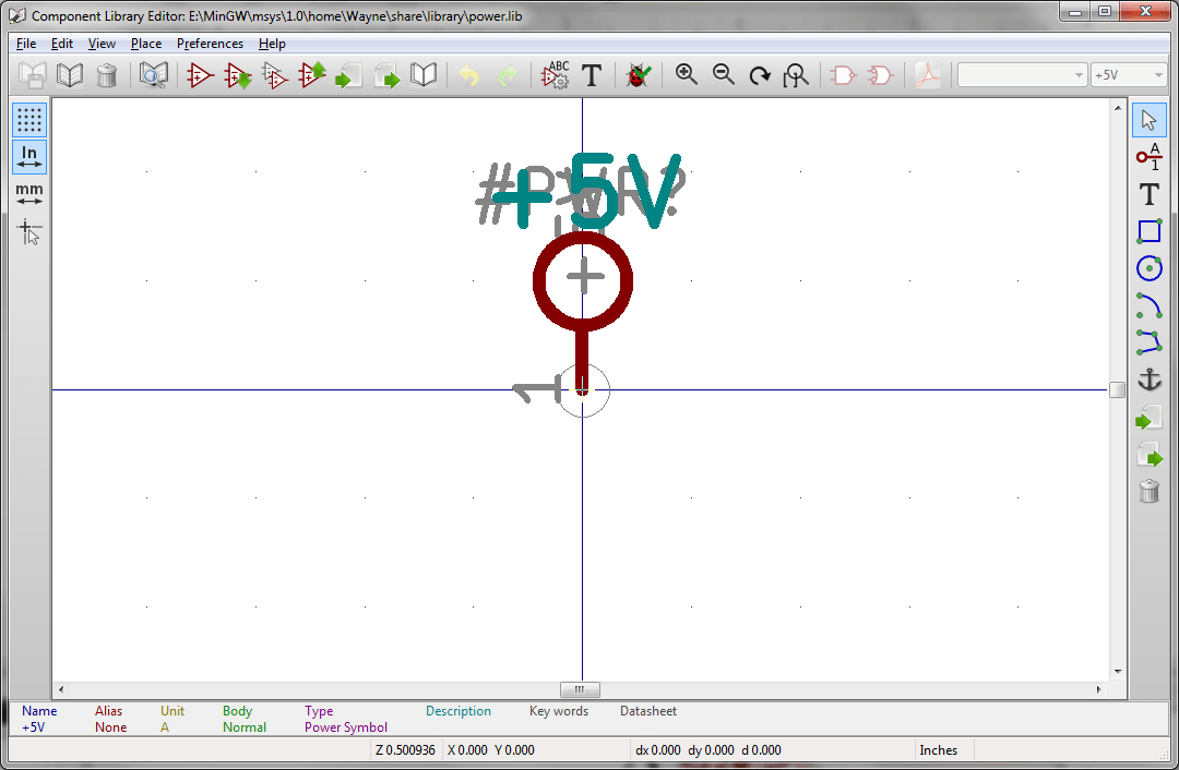
Para crear un símbolo de potencia siga los siguientes pasos:
-
Añada un pin de tipo "Pin de entrada de potencia" llamado +5V (esto es importante porque este nombre establecerá una conexión a la red +5V) con número de pin 1 (el numero no es relevante), una longitud de 0, y un estilo gráfico tipo "Linea"
-
Coloque un pequeño círculo y un segmento desde el pin hasta el círculo tal y como se muestra.
-
El punto de anclaje del símbolo esta en el pin.
-
The symbol value is
+5V. -
The symbol reference is
#+5V. The reference text is not important except the first character which must be#to indicate that the symbol is a power symbol. By convention, every symbol in which the reference field starts with a#will not appear in the symbol list or in the netlist and the reference is declared as invisible.
Una manera mas fácil de crear un nuevo símbolo de potencia es usar otro símbolo como modelo.
-
Cargue un símbolo de potencia existente.
-
Edite el nombre del pin con el nombre del nuevo símbolo de potencia.
-
Edite el campo "valor" con el mismo nombre que el pin, si desea mostrar el valor del símbolo de potencia.
-
Save the new symbol.
LibEdit - Symbols
Resumen
A symbol consist of the following elements
-
Una representación gráfica (formas geométricas, textos).
-
Pines.
-
Fields or associated text used by the post processors: netlist, symbols list.
Two fields are to be initialized: reference and value. The name of the design associated with the symbol, and the name of the associated footprint, the other fields are the free fields, they can generally remain empty, and could be filled during schematic capture.
However, managing the documentation associated with any symbol facilitates the research, use and maintenance of libraries. The associated documentation consists of
-
Una línea de comentarios
-
Una línea de palabras clave como TTL CMOS NAND2, separadas por espacios.
-
Un nombre de fichero adjunto (por ejemplo una nota de aplicación o un fichero pdf)
El directorio por defecto de ficheros adjuntos:
kicad/share/library/doc
Si no se encuentra:
kicad/library/doc
Bajo linux:
/usr/local/kicad/share/library/doc
/usr/share/kicad/library/doc
/usr/local/share/kicad/library/doc
Key words allow you to selectively search for a symbol according to various selection criteria. Comments and key words are displayed in various menus, and particularly when you select a symbol from the library.
The symbol also has an anchoring point. A rotation or a mirror is made relative to this anchor point and during a placement this point is used as a reference position. It is thus useful to position this anchor accurately.
A symbol can have aliases, i.e. equivalent names. This allows you to considerably reduce the number of symbols that need to be created (for example, a 74LS00 can have aliases such as 74000, 74HC00, 74HCT00…).
Finally, the symbols are distributed in libraries (classified by topics, or manufacturer) in order to facilitate their management.
Position a symbol anchor
El punto de anclaje es la coordenada (0,0) y es representado mediante los ejes azules mostrados en la pantalla.
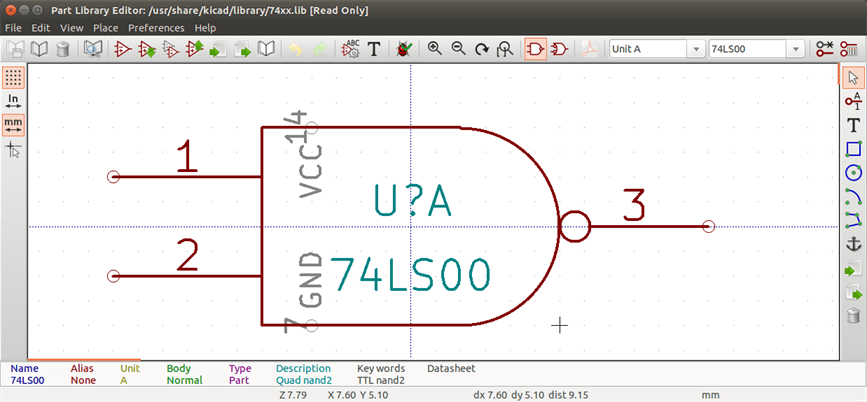
El punto de anclaje puede ser reubicado seleccionando el icono ![]() y haciendo clic sobre en nuevo punto de anclaje deseado. El dibujo será automáticamente re-centrado sobre el nuevo punto de anclaje.
y haciendo clic sobre en nuevo punto de anclaje deseado. El dibujo será automáticamente re-centrado sobre el nuevo punto de anclaje.
Symbol aliases
An alias is another name corresponding to the same symbol in the library. Symbols with similar pin-out and representation can then be represented by only one symbol, having several aliases (e.g. 7400 with alias 74LS00, 74HC00, 74LS37 ).
El uso de alias le permite crear bibliotecas completas rápidamente. Además, estas bibliotecas al ser mas compactas son cargadas mas fácil por KiCad.
Para modificar la lista de alias, debe seleccionar la ventana principal de edición vía el icono ![]() y seleccionar la pestaña alias.
y seleccionar la pestaña alias.
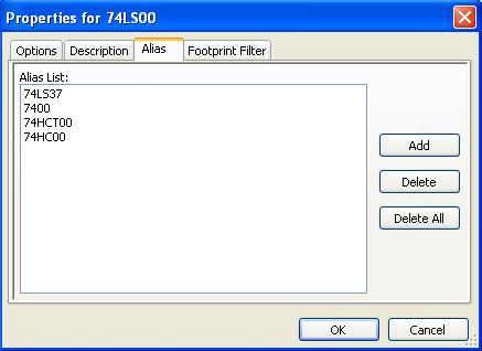
Puede, de este modo, añadir o eliminar los alias deseado. El alias del componente actual no puede ser eliminado, obviamente, mientras este siendo editado.
To remove all aliases, you have firstly to select the root symbol. The first symbol in the alias list in the window of selection of the main toolbar.
Symbol fields
The field editor is called via the icon ![]() .
.
There are four special fields (texts attached to the symbol), and configurable user fields
Campos especiales
-
Referencia.
-
Value. It is the symbol name in the library and the default value field in schematic.
-
Huella. Es la el nombre de la huella usado en la placa. No es muy útil si se utiliza CvPcb para configurar la lista de huellas, pero obligatorio si CvPcb no se usa.
-
Hoja. Es un campo reservado, no usado durante el tiempo de edición.
Symbol documentation
To edit documentation information, it is necessary to call the main editing window of the symbol via the icon ![]() and to select the document folder.
and to select the document folder.
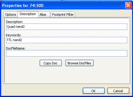
Be sure to select the right alias, or the root symbol, because this documentation is the only characteristic which differs between aliases. The "Copy Doc" button allows you to copy the documentation information from the root symbol towards the currently edited alias.
Symbol keywords
Keywords allow you to search in a selective way for a symbol according to specific selection criteria (function, technological family, etc.)
La herramienta de búsqueda de Eeschema no es sensible a mayúsculas. Las palabras clave típicas en las bibliotecas son:
-
CMOS TTL para las familias lógicas.
-
AND2 NOR3 XOR2 INV… para las puertas (AND2 = puerta AND de 2 entradas, NOR3 = puerta NOR de 3 entradas)
-
JKFF DFF… para los flip-flop tipo JK o tipo D.
-
ADC, DAC, MUX…
-
OpenCol for the gates with open collector output. Thus if in the schematic capture software, you search the symbol: by keywords NAND2 OpenCol Eeschema will display the list of symbols having these 2 key words.
Symbol documentation (Doc)
The line of comment (and keywords) is displayed in various menus, particularly when you select a symbol in the displayed symbols list of a library and in the ViewLib menu.
If this Doc. file exists, it is also accessible in the schematic capture software, in the pop-up menu displayed by right-clicking on the symbol.
Fichero de documentación asociado (DocFileName)
Indica un fichero adjunto (documentación, notas de aplicación) disponible (fichero pdf, diagrama de esquema, etc).
Filtrado de huella para CvPcb
You can enter a list of allowed footprints for the symbol. This list acts as a filter used by CvPcb to display only the allowed footprints. A void list does not filter anything.
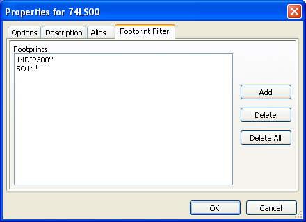
Están permitidos los metacaracteres.
SO14* permite a CvPcb mostrar todos las huellas cuyo nombre comience por S014.
Para una resistencia, R? muestra todas las huellas de 2 letras que comiencen por R.
Aquí hay unos ejemplos: con y sin filtrado.
Con filtrado.
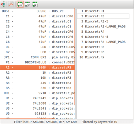
Sin filtrado
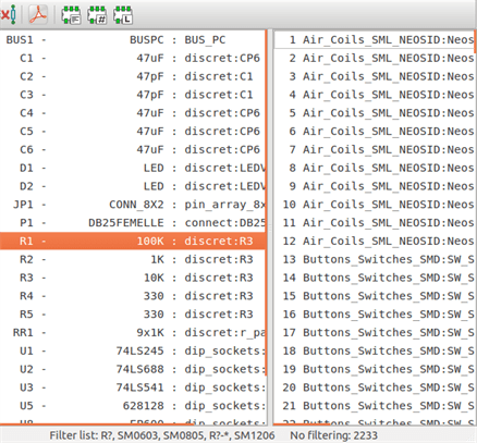
Biblioteca de símbolos
You can easily compile a graphic symbols library file containing frequently used symbols. This can be used for the creation of symbols (triangles, the shape of AND, OR, Exclusive OR gates, etc.) for saving and subsequent re-use.
These files are stored by default in the library directory and have a '.sym' extension. These symbols are not gathered in libraries like the normal symbols because they are generally not so many.
Exportar o crear un símbolo
A symbol can be exported with the button ![]() . You can generally create only one graphic, also it will be a good idea to delete all pins, if they exist.
. You can generally create only one graphic, also it will be a good idea to delete all pins, if they exist.
Importar un símbolo
Importing allows you to add graphics to a symbol you are editing. A symbol is imported with the button ![]() . Imported graphics are added as they were created in existing graphics.
. Imported graphics are added as they were created in existing graphics.
Symbol Library Browser
Introducción
The Symbol Library Browser allows you to quickly examine the content of symbol libraries. The Symbol Library Viewer can be accessed by clicking ![]() icon on the main toolbar, selecting "Library Browser" entry in the "View" menu or double clicking symbol image on "Choose Symbol" window.
icon on the main toolbar, selecting "Library Browser" entry in the "View" menu or double clicking symbol image on "Choose Symbol" window.
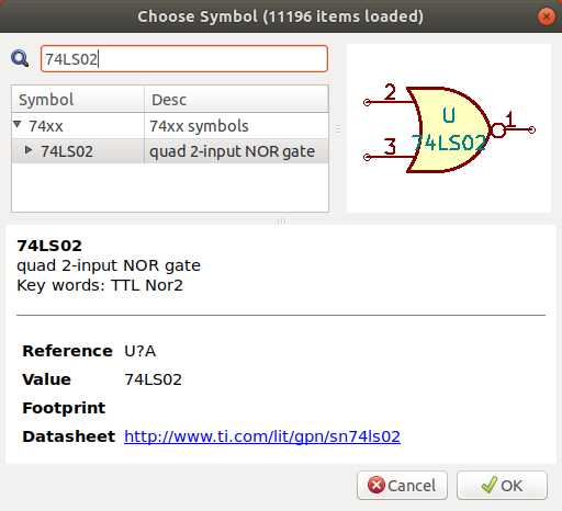
Viewlib - pantalla principal
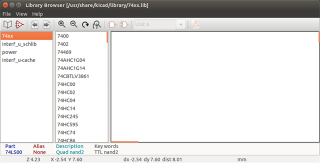
To examine the contents of a library, select a library from the list on the left hand pane. All symbols in the selected library will appear in the second pane. Select a symbol name to view the symbol.
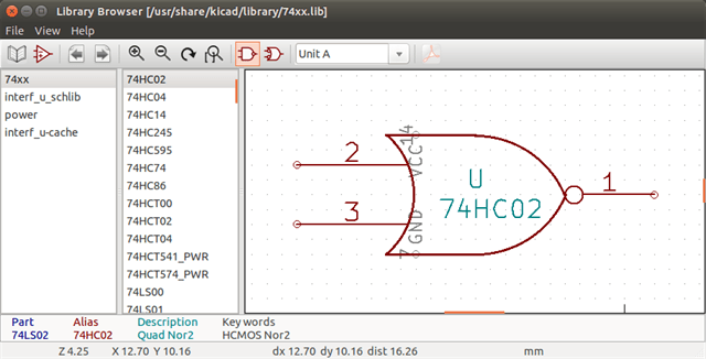
Symbol Library Browser Top Toolbar
The top tool bar in Symbol Library Brower is shown below.

The available commands are:
|
Selection of the desired library which can be also selected in the displayed list. |
|
Selection of the symbol which can be also selected in the displayed list. |
|
Display previous symbol. |
|
Display next symbol. |
|
Zoom tools. |
|
Selection of the representation (normal or converted) if exist. |
|
Selection of the unit for symbols that contain multiple units. |
|
If it exist, display the associated documents. Exists only when called by the place symbol dialog frame from Eeschema. |
|
Close the browser and place the selected symbol in Eeschema. This icon is only displayed when browser has been called from Eeschema (double click on a symbol in the component chooser). |

Creando Netlists y Ficheros BOM Personalizados
Ficheros Netlist Intermedios
Ficheros BOM y netlist pueden ser convertidos desde un fichero netlist intermedio creado por Eeschema.
Este fichero usa sintaxis XML y es llamado el netlist intermedio. Este netlist intermedio incluye gran cantidad de datos sobre su placa y por ello puede ser usado mediante post-procesamiento para crear una lista BOM u otros informes.
Dependiendo de la salida (BOM o netlist), diferentes subconjuntos del fichero netlist intermedio completo serán usados en el post-procesado.
Ejemplo de Esquema
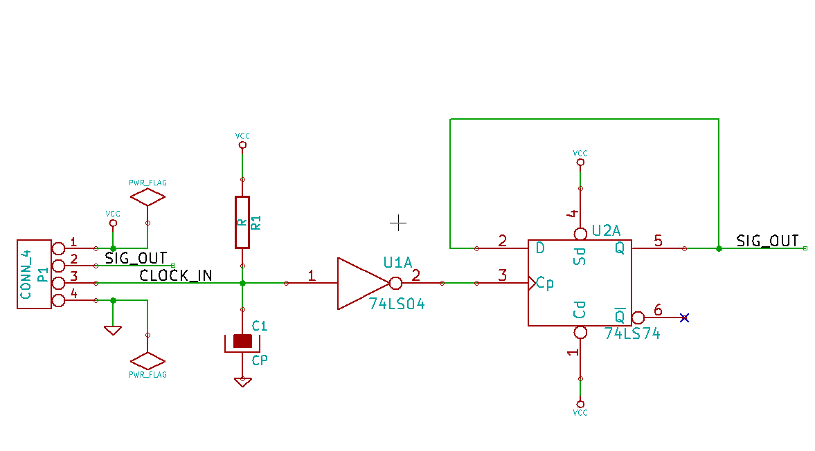
Ejemplo del fichero Netlist Intermedio
El netlist intermedio correspondiente (usando sintaxis XML) al circuito anterior es mostrado a continuación.
<?xml version="1.0" encoding="utf-8"?>
<export version="D">
<design>
<source>F:\kicad_aux\netlist_test\netlist_test.sch</source>
<date>29/08/2010 20:35:21</date>
<tool>eeschema (2010-08-28 BZR 2458)-unstable</tool>
</design>
<components>
<comp ref="P1">
<value>CONN_4</value>
<libsource lib="conn" part="CONN_4"/>
<sheetpath names="/" tstamps="/"/>
<tstamp>4C6E2141</tstamp>
</comp>
<comp ref="U2">
<value>74LS74</value>
<libsource lib="74xx" part="74LS74"/>
<sheetpath names="/" tstamps="/"/>
<tstamp>4C6E20BA</tstamp>
</comp>
<comp ref="U1">
<value>74LS04</value>
<libsource lib="74xx" part="74LS04"/>
<sheetpath names="/" tstamps="/"/>
<tstamp>4C6E20A6</tstamp>
</comp>
<comp ref="C1">
<value>CP</value>
<libsource lib="device" part="CP"/>
<sheetpath names="/" tstamps="/"/>
<tstamp>4C6E2094</tstamp>
</comp>
<comp ref="R1">
<value>R</value>
<libsource lib="device" part="R"/>
<sheetpath names="/" tstamps="/"/>
<tstamp>4C6E208A</tstamp>
</comp>
</components>
<libparts>
<libpart lib="device" part="C">
<description>Condensateur non polarise</description>
<footprints>
<fp>SM*</fp>
<fp>C?</fp>
<fp>C1-1</fp>
</footprints>
<fields>
<field name="Reference">C</field>
<field name="Value">C</field>
</fields>
<pins>
<pin num="1" name="~" type="passive"/>
<pin num="2" name="~" type="passive"/>
</pins>
</libpart>
<libpart lib="device" part="R">
<description>Resistance</description>
<footprints>
<fp>R?</fp>
<fp>SM0603</fp>
<fp>SM0805</fp>
<fp>R?-*</fp>
<fp>SM1206</fp>
</footprints>
<fields>
<field name="Reference">R</field>
<field name="Value">R</field>
</fields>
<pins>
<pin num="1" name="~" type="passive"/>
<pin num="2" name="~" type="passive"/>
</pins>
</libpart>
<libpart lib="conn" part="CONN_4">
<description>Symbole general de connecteur</description>
<fields>
<field name="Reference">P</field>
<field name="Value">CONN_4</field>
</fields>
<pins>
<pin num="1" name="P1" type="passive"/>
<pin num="2" name="P2" type="passive"/>
<pin num="3" name="P3" type="passive"/>
<pin num="4" name="P4" type="passive"/>
</pins>
</libpart>
<libpart lib="74xx" part="74LS04">
<description>Hex Inverseur</description>
<fields>
<field name="Reference">U</field>
<field name="Value">74LS04</field>
</fields>
<pins>
<pin num="1" name="~" type="input"/>
<pin num="2" name="~" type="output"/>
<pin num="3" name="~" type="input"/>
<pin num="4" name="~" type="output"/>
<pin num="5" name="~" type="input"/>
<pin num="6" name="~" type="output"/>
<pin num="7" name="GND" type="power_in"/>
<pin num="8" name="~" type="output"/>
<pin num="9" name="~" type="input"/>
<pin num="10" name="~" type="output"/>
<pin num="11" name="~" type="input"/>
<pin num="12" name="~" type="output"/>
<pin num="13" name="~" type="input"/>
<pin num="14" name="VCC" type="power_in"/>
</pins>
</libpart>
<libpart lib="74xx" part="74LS74">
<description>Dual D FlipFlop, Set & Reset</description>
<docs>74xx/74hc_hct74.pdf</docs>
<fields>
<field name="Reference">U</field>
<field name="Value">74LS74</field>
</fields>
<pins>
<pin num="1" name="Cd" type="input"/>
<pin num="2" name="D" type="input"/>
<pin num="3" name="Cp" type="input"/>
<pin num="4" name="Sd" type="input"/>
<pin num="5" name="Q" type="output"/>
<pin num="6" name="~Q" type="output"/>
<pin num="7" name="GND" type="power_in"/>
<pin num="8" name="~Q" type="output"/>
<pin num="9" name="Q" type="output"/>
<pin num="10" name="Sd" type="input"/>
<pin num="11" name="Cp" type="input"/>
<pin num="12" name="D" type="input"/>
<pin num="13" name="Cd" type="input"/>
<pin num="14" name="VCC" type="power_in"/>
</pins>
</libpart>
</libparts>
<libraries>
<library logical="device">
<uri>F:\kicad\share\library\device.lib</uri>
</library>
<library logical="conn">
<uri>F:\kicad\share\library\conn.lib</uri>
</library>
<library logical="74xx">
<uri>F:\kicad\share\library\74xx.lib</uri>
</library>
</libraries>
<nets>
<net code="1" name="GND">
<node ref="U1" pin="7"/>
<node ref="C1" pin="2"/>
<node ref="U2" pin="7"/>
<node ref="P1" pin="4"/>
</net>
<net code="2" name="VCC">
<node ref="R1" pin="1"/>
<node ref="U1" pin="14"/>
<node ref="U2" pin="4"/>
<node ref="U2" pin="1"/>
<node ref="U2" pin="14"/>
<node ref="P1" pin="1"/>
</net>
<net code="3" name="">
<node ref="U2" pin="6"/>
</net>
<net code="4" name="">
<node ref="U1" pin="2"/>
<node ref="U2" pin="3"/>
</net>
<net code="5" name="/SIG_OUT">
<node ref="P1" pin="2"/>
<node ref="U2" pin="5"/>
<node ref="U2" pin="2"/>
</net>
<net code="6" name="/CLOCK_IN">
<node ref="R1" pin="2"/>
<node ref="C1" pin="1"/>
<node ref="U1" pin="1"/>
<node ref="P1" pin="3"/>
</net>
</nets>
</export>
Conversión a un nuevo formato de netlist
Aplicando un filtro de post-procesado al fichero netlist intermedio puede generar ficheros netlist en otros formatos, así como ficheros de listas BOM. Como esta conversión es una transformación tipo texto a texto, este filtro de post-procesado puede ser escrito usando Python, XSLT, u otra herramienta capaz de aceptar XML como entrada
XSLT itself is an XML language very suitable for XML transformations. There is a free program called xsltproc that you can download and install. The xsltproc program can be used to read the Intermediate XML netlist input file, apply a style-sheet to transform the input, and save the results in an output file. Use of xsltproc requires a style-sheet file using XSLT conventions. The full conversion process is handled by Eeschema, after it is configured once to run xsltproc in a specific way.
Introduccion de XSLT
El documento que describe las transformaciones XSL (XSLT) está disponible aqui:
Crear un fichero netlist Pads-Pcb
El formato pads-pcb está compuesto por dos secciones.
-
La lista de huellas.
-
La lista de nodos: Agrupando las referencias de los pads por nodos.
Justo debajo se muestra una hoja de estilo que convierte el fichero netlist intermedio al formato netlist pads-pcb:
<?xml version="1.0" encoding="ISO-8859-1"?>
<!--XSL style sheet to Eeschema Generic Netlist Format to PADS netlist format
Copyright (C) 2010, SoftPLC Corporation.
GPL v2.
How to use:
https://lists.launchpad.net/kicad-developers/msg05157.html
-->
<!DOCTYPE xsl:stylesheet [
<!ENTITY nl "
"> <!--new line CR, LF -->
]>
<xsl:stylesheet version="1.0" xmlns:xsl="http://www.w3.org/1999/XSL/Transform">
<xsl:output method="text" omit-xml-declaration="yes" indent="no"/>
<xsl:template match="/export">
<xsl:text>*PADS-PCB*&nl;*PART*&nl;</xsl:text>
<xsl:apply-templates select="components/comp"/>
<xsl:text>&nl;*NET*&nl;</xsl:text>
<xsl:apply-templates select="nets/net"/>
<xsl:text>*END*&nl;</xsl:text>
</xsl:template>
<!-- for each component -->
<xsl:template match="comp">
<xsl:text> </xsl:text>
<xsl:value-of select="@ref"/>
<xsl:text> </xsl:text>
<xsl:choose>
<xsl:when test = "footprint != '' ">
<xsl:apply-templates select="footprint"/>
</xsl:when>
<xsl:otherwise>
<xsl:text>unknown</xsl:text>
</xsl:otherwise>
</xsl:choose>
<xsl:text>&nl;</xsl:text>
</xsl:template>
<!-- for each net -->
<xsl:template match="net">
<!-- nets are output only if there is more than one pin in net -->
<xsl:if test="count(node)>1">
<xsl:text>*SIGNAL* </xsl:text>
<xsl:choose>
<xsl:when test = "@name != '' ">
<xsl:value-of select="@name"/>
</xsl:when>
<xsl:otherwise>
<xsl:text>N-</xsl:text>
<xsl:value-of select="@code"/>
</xsl:otherwise>
</xsl:choose>
<xsl:text>&nl;</xsl:text>
<xsl:apply-templates select="node"/>
</xsl:if>
</xsl:template>
<!-- for each node -->
<xsl:template match="node">
<xsl:text> </xsl:text>
<xsl:value-of select="@ref"/>
<xsl:text>.</xsl:text>
<xsl:value-of select="@pin"/>
<xsl:text>&nl;</xsl:text>
</xsl:template>
</xsl:stylesheet>
Y aquí se muestra el fichero de salida tipo netlist pads-pcb tras ejecutar xsltproc:
*PADS-PCB*
*PART*
P1 unknown
U2 unknown
U1 unknown
C1 unknown
R1 unknown
*NET*
*SIGNAL* GND
U1.7
C1.2
U2.7
P1.4
*SIGNAL* VCC
R1.1
U1.14
U2.4
U2.1
U2.14
P1.1
*SIGNAL* N-4
U1.2
U2.3
*SIGNAL* /SIG_OUT
P1.2
U2.5
U2.2
*SIGNAL* /CLOCK_IN
R1.2
C1.1
U1.1
P1.3

*END*
La linea de comando para realizar esta conversión es:
kicad\\bin\\xsltproc.exe -o test.net kicad\\bin\\plugins\\netlist_form_pads-pcb.xsl test.tmp
Crear un fichero netlist tipo Cadstar
El formato Cadstar está compuesto por dos secciones.
-
La lista de huellas.
-
La lista de nodos: Agrupando las referencias de los pads por nodos.
Aquí se muestra un fichero de hoja de estilo que realiza esta conversión:
<?xml version="1.0" encoding="ISO-8859-1"?>
<!--XSL style sheet to Eeschema Generic Netlist Format to CADSTAR netlist format
Copyright (C) 2010, Jean-Pierre Charras.
Copyright (C) 2010, SoftPLC Corporation.
GPL v2.
<!DOCTYPE xsl:stylesheet [
<!ENTITY nl "
"> <!--new line CR, LF -->
]>
<xsl:stylesheet version="1.0" xmlns:xsl="http://www.w3.org/1999/XSL/Transform">
<xsl:output method="text" omit-xml-declaration="yes" indent="no"/>
<!-- Netlist header -->
<xsl:template match="/export">
<xsl:text>.HEA&nl;</xsl:text>
<xsl:apply-templates select="design/date"/> <!-- Generate line .TIM <time> -->
<xsl:apply-templates select="design/tool"/> <!-- Generate line .APP <eeschema version> -->
<xsl:apply-templates select="components/comp"/> <!-- Generate list of components -->
<xsl:text>&nl;&nl;</xsl:text>
<xsl:apply-templates select="nets/net"/> <!-- Generate list of nets and connections -->
<xsl:text>&nl;.END&nl;</xsl:text>
</xsl:template>
<!-- Generate line .TIM 20/08/2010 10:45:33 -->
<xsl:template match="tool">
<xsl:text>.APP "</xsl:text>
<xsl:apply-templates/>
<xsl:text>"&nl;</xsl:text>
</xsl:template>
<!-- Generate line .APP "eeschema (2010-08-17 BZR 2450)-unstable" -->
<xsl:template match="date">
<xsl:text>.TIM </xsl:text>
<xsl:apply-templates/>
<xsl:text>&nl;</xsl:text>
</xsl:template>
<!-- for each component -->
<xsl:template match="comp">
<xsl:text>.ADD_COM </xsl:text>
<xsl:value-of select="@ref"/>
<xsl:text> </xsl:text>
<xsl:choose>
<xsl:when test = "value != '' ">
<xsl:text>"</xsl:text> <xsl:apply-templates select="value"/> <xsl:text>"</xsl:text>
</xsl:when>
<xsl:otherwise>
<xsl:text>""</xsl:text>
</xsl:otherwise>
</xsl:choose>
<xsl:text>&nl;</xsl:text>
</xsl:template>
<!-- for each net -->
<xsl:template match="net">
<!-- nets are output only if there is more than one pin in net -->
<xsl:if test="count(node)>1">
<xsl:variable name="netname">
<xsl:text>"</xsl:text>
<xsl:choose>
<xsl:when test = "@name != '' ">
<xsl:value-of select="@name"/>
</xsl:when>
<xsl:otherwise>
<xsl:text>N-</xsl:text>
<xsl:value-of select="@code"/>
</xsl:otherwise>
</xsl:choose>
<xsl:text>"&nl;</xsl:text>
</xsl:variable>
<xsl:apply-templates select="node" mode="first"/>
<xsl:value-of select="$netname"/>
<xsl:apply-templates select="node" mode="others"/>
</xsl:if>
</xsl:template>
<xsl:template match="node" mode="others">
<xsl:choose>
<xsl:when test='position()=1'>
</xsl:when>
<xsl:when test='position()=2'>
<xsl:text>.TER </xsl:text>
</xsl:when>
<xsl:otherwise>
<xsl:text> </xsl:text>
</xsl:otherwise>
</xsl:choose>
<xsl:if test="position()>1">
<xsl:value-of select="@ref"/>
<xsl:text>.</xsl:text>
<xsl:value-of select="@pin"/>
<xsl:text>&nl;</xsl:text>
</xsl:if>
</xsl:template>
</xsl:stylesheet>
A continuación se muestra el fichero de salida formato Caadstar.
.HEA
.TIM 21/08/2010 08:12:08
.APP "eeschema (2010-08-09 BZR 2439)-unstable"
.ADD_COM P1 "CONN_4"
.ADD_COM U2 "74LS74"
.ADD_COM U1 "74LS04"
.ADD_COM C1 "CP"
.ADD_COM R1 "R"


.ADD_TER U1.7 "GND"
.TER     C1.2
         U2.7
         P1.4
.ADD_TER R1.1 "VCC"
.TER     U1.14
         U2.4
         U2.1
         U2.14
         P1.1
.ADD_TER U1.2 "N-4"
.TER     U2.3
.ADD_TER P1.2 "/SIG_OUT"
.TER     U2.5
         U2.2
.ADD_TER R1.2 "/CLOCK_IN"
.TER     C1.1
         U1.1
         P1.3

.END
Create an OrcadPCB2 netlist file
Este formato tiene solo una sección que es la lista de huellas. Cada huella incluye su lista de pads con referencias a nodos.
Aqui se muestra la hoja de estilo para esta conversión:
<?xml version="1.0" encoding="ISO-8859-1"?>
<!--XSL style sheet to Eeschema Generic Netlist Format to CADSTAR netlist format
Copyright (C) 2010, SoftPLC Corporation.
GPL v2.
How to use:
https://lists.launchpad.net/kicad-developers/msg05157.html
-->
<!DOCTYPE xsl:stylesheet [
<!ENTITY nl "
"> <!--new line CR, LF -->
]>
<xsl:stylesheet version="1.0" xmlns:xsl="http://www.w3.org/1999/XSL/Transform">
<xsl:output method="text" omit-xml-declaration="yes" indent="no"/>
<!--
Netlist header
Creates the entire netlist
(can be seen as equivalent to main function in C
-->
<xsl:template match="/export">
<xsl:text>( { Eeschema Netlist Version 1.1 </xsl:text>
<!-- Generate line .TIM <time> -->
<xsl:apply-templates select="design/date"/>
<!-- Generate line eeschema version ... -->
<xsl:apply-templates select="design/tool"/>
<xsl:text>}&nl;</xsl:text>
<!-- Generate the list of components -->
<xsl:apply-templates select="components/comp"/> <!-- Generate list of components -->
<!-- end of file -->
<xsl:text>)&nl;*&nl;</xsl:text>
</xsl:template>
<!--
Generate id in header like "eeschema (2010-08-17 BZR 2450)-unstable"
-->
<xsl:template match="tool">
<xsl:apply-templates/>
</xsl:template>
<!--
Generate date in header like "20/08/2010 10:45:33"
-->
<xsl:template match="date">
<xsl:apply-templates/>
<xsl:text>&nl;</xsl:text>
</xsl:template>
<!--
This template read each component
(path = /export/components/comp)
creates lines:
( 3EBF7DBD $noname U1 74LS125
... pin list ...
)
and calls "create_pin_list" template to build the pin list
-->
<xsl:template match="comp">
<xsl:text> ( </xsl:text>
<xsl:choose>
<xsl:when test = "tstamp != '' ">
<xsl:apply-templates select="tstamp"/>
</xsl:when>
<xsl:otherwise>
<xsl:text>00000000</xsl:text>
</xsl:otherwise>
</xsl:choose>
<xsl:text> </xsl:text>
<xsl:choose>
<xsl:when test = "footprint != '' ">
<xsl:apply-templates select="footprint"/>
</xsl:when>
<xsl:otherwise>
<xsl:text>$noname</xsl:text>
</xsl:otherwise>
</xsl:choose>
<xsl:text> </xsl:text>
<xsl:value-of select="@ref"/>
<xsl:text> </xsl:text>
<xsl:choose>
<xsl:when test = "value != '' ">
<xsl:apply-templates select="value"/>
</xsl:when>
<xsl:otherwise>
<xsl:text>"~"</xsl:text>
</xsl:otherwise>
</xsl:choose>
<xsl:text>&nl;</xsl:text>
<xsl:call-template name="Search_pin_list" >
<xsl:with-param name="cmplib_id" select="libsource/@part"/>
<xsl:with-param name="cmp_ref" select="@ref"/>
</xsl:call-template>
<xsl:text> )&nl;</xsl:text>
</xsl:template>
<!--
This template search for a given lib component description in list
lib component descriptions are in /export/libparts,
and each description start at ./libpart
We search here for the list of pins of the given component
This template has 2 parameters:
"cmplib_id" (reference in libparts)
"cmp_ref" (schematic reference of the given component)
-->
<xsl:template name="Search_pin_list" >
<xsl:param name="cmplib_id" select="0" />
<xsl:param name="cmp_ref" select="0" />
<xsl:for-each select="/export/libparts/libpart">
<xsl:if test = "@part = $cmplib_id ">
<xsl:apply-templates name="build_pin_list" select="pins/pin">
<xsl:with-param name="cmp_ref" select="$cmp_ref"/>
</xsl:apply-templates>
</xsl:if>
</xsl:for-each>
</xsl:template>
<!--
This template writes the pin list of a component
from the pin list of the library description
The pin list from library description is something like
<pins>
<pin num="1" type="passive"/>
<pin num="2" type="passive"/>
</pins>
Output pin list is ( <pin num> <net name> )
something like
( 1 VCC )
( 2 GND )
-->
<xsl:template name="build_pin_list" match="pin">
<xsl:param name="cmp_ref" select="0" />
<!-- write pin numner and separator -->
<xsl:text> ( </xsl:text>
<xsl:value-of select="@num"/>
<xsl:text> </xsl:text>
<!-- search net name in nets section and write it: -->
<xsl:variable name="pinNum" select="@num" />
<xsl:for-each select="/export/nets/net">
<!-- net name is output only if there is more than one pin in net
else use "?" as net name, so count items in this net
-->
<xsl:variable name="pinCnt" select="count(node)" />
<xsl:apply-templates name="Search_pin_netname" select="node">
<xsl:with-param name="cmp_ref" select="$cmp_ref"/>
<xsl:with-param name="pin_cnt_in_net" select="$pinCnt"/>
<xsl:with-param name="pin_num"> <xsl:value-of select="$pinNum"/>
</xsl:with-param>
</xsl:apply-templates>
</xsl:for-each>
<!-- close line -->
<xsl:text> )&nl;</xsl:text>
</xsl:template>
<!--
This template writes the pin netname of a given pin of a given component
from the nets list
The nets list description is something like
<nets>
<net code="1" name="GND">
<node ref="J1" pin="20"/>
<node ref="C2" pin="2"/>
</net>
<net code="2" name="">
<node ref="U2" pin="11"/>
</net>
</nets>
This template has 2 parameters:
"cmp_ref" (schematic reference of the given component)
"pin_num" (pin number)
-->
<xsl:template name="Search_pin_netname" match="node">
<xsl:param name="cmp_ref" select="0" />
<xsl:param name="pin_num" select="0" />
<xsl:param name="pin_cnt_in_net" select="0" />
<xsl:if test = "@ref = $cmp_ref ">
<xsl:if test = "@pin = $pin_num">
<!-- net name is output only if there is more than one pin in net
else use "?" as net name
-->
<xsl:if test = "$pin_cnt_in_net>1">
<xsl:choose>
<!-- if a net has a name, use it,
else build a name from its net code
-->
<xsl:when test = "../@name != '' ">
<xsl:value-of select="../@name"/>
</xsl:when>
<xsl:otherwise>
<xsl:text>$N-0</xsl:text><xsl:value-of select="../@code"/>
</xsl:otherwise>
</xsl:choose>
</xsl:if>
<xsl:if test = "$pin_cnt_in_net <2">
<xsl:text>?</xsl:text>
</xsl:if>
</xsl:if>
</xsl:if>
</xsl:template>
</xsl:stylesheet>
Este es el fichero de salida en formato OrcadPCB2
( { Eeschema Netlist Version 1.1  29/08/2010 21:07:51
eeschema (2010-08-28 BZR 2458)-unstable}
 ( 4C6E2141 $noname P1 CONN_4
  (  1 VCC )
  (  2 /SIG_OUT )
  (  3 /CLOCK_IN )
  (  4 GND )
 )
 ( 4C6E20BA $noname U2 74LS74
  (  1 VCC )
  (  2 /SIG_OUT )
  (  3 N-04 )
  (  4 VCC )
  (  5 /SIG_OUT )
  (  6 ? )
  (  7 GND )
  (  14 VCC )
 )
 ( 4C6E20A6 $noname U1 74LS04
  (  1 /CLOCK_IN )
  (  2 N-04 )
  (  7 GND )
  (  14 VCC )
 )
 ( 4C6E2094 $noname C1 CP
  (  1 /CLOCK_IN )
  (  2 GND )
 )
 ( 4C6E208A $noname R1 R
  (  1 VCC )
  (  2 /CLOCK_IN )
 )
)
*
Interfaz de plugins de Eeschema
Los conversores de netlist intermedio pueden ser automáticamente ejecutados dentro de Eeschema.
Inicie la ventana de dialogo
Ahora puede añadir una nueva interfaz de usuario para el netlist plug-in haciendo clic sobre el botón "Añadir Plugin".
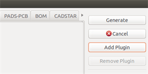
A continuación se muestra el aspecto de los datos de configuración para el formato PadsPcb.
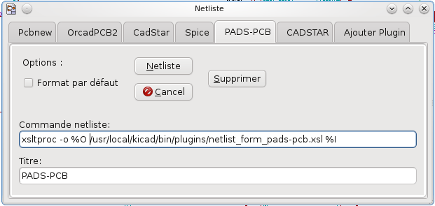
Parámetros de configuración de Plugins
La ventana de configuración de plug-in en Eeschema necesita la siguiente información:
-
El título: por ejemplo, el nombre del formato de netlist.
-
La comando para lanzar el conversor.
Una vez que hace clic en el boto netlist sucede lo siguiente:
-
Eeschema crea un fichero netlist intermedio *.xml, por ejemplo test.xml.
-
Eeschema ejecuta el plug-in leyendo test.xml y crea test.net
Generar ficheros netlist bajo linea de comando.
Suponiendo que estamos usando el programa xsltproc.exe para aplicar la hoja de estilo al fichero intermedio, xsltproc.exe se ejecutará con el siguiente comando:
xsltproc.exe -o <output filename> < style-sheet filename> <input XML file to convert>
En KiCad bajo Windows la linea de comando es la siguiente:
f:/kicad/bin/xsltproc.exe -o "%O" f:/kicad/bin/plugins/netlist_form_pads-pcb.xsl "%I"
Bajo Linux la linea de comando es como sigue:
xsltproc -o "%O" /usr/local/kicad/bin/plugins/netlist_form_pads-pcb.xsl "%I"
Donde netlist_form_pads-pcb.xsl es la hoja de estilo que se esta aplicando. No olvide las comillas dobles en el nombre del fichero, esto le permite tener espacios tras la sustitución por Eeschema.
El formato de los comandos acepta parámetros como nombres de archivo.
El formato de los parámetros admitidos es:
-
%B ⇒ nombre de archivo base y ruta del fichero de salida seleccionado, menos la ruta y extensión.
-
%I ⇒ nombre de archivo completo y ruta del fichero temporal de entrada (el fichero netlist intermedio)
-
%O ⇒ nombre de archivo completo y ruta del fichero de salida elegido.
%I será reemplazado por el nombre de archivo del fichero intermedio actual.
%O será reemplazado por el nombre de archivo del fichero de salida actual.
Formato del comando: ejemplo para xsltproc
El formato del comando para xsltproc es el siguiente:
<path of xsltproc> xsltproc <xsltproc parameters>
bajo Windows:
f:/kicad/bin/xsltproc.exe -o "%O" f:/kicad/bin/plugins/netlist_form_pads-pcb.xsl "%I"
bajo Linux:
xsltproc -o "%O" /usr/local/kicad/bin/plugins/netlist_form_pads-pcb.xsl "%I"
Los ejemplos anteriores suponen que xsltproc esta instalado en su PC bajo Windows y todos los ficheros están ubicados en kicad/bin.
Generación de Listas de Materiales
Dado que el netlist intermedio contiene toda la información sobre los componentes usados, una lista BOM puede ser extraída de el. Aquí se muestra la ventana de ajuste del plug-in (en Linux) para crear un fichero de lista de materiales (BOM) personalizado:
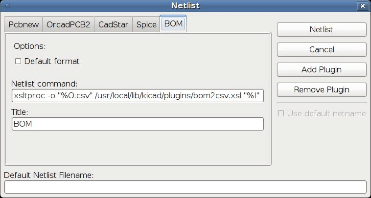
La ruta al archivo de hoja de estilo bom2csv.xsl depende del sistema empleado. La mejor hoja de estilo XSLT actualmente para la generación de listas de materiales es llamada bom2csv.xsl. Siéntase libre de modificarla de acuerdo a sus necesidades, y si desarrolla algo útil en general, pregunte para que forme parte del proyecto kiCad.
Formato de Comandos: ejemplos para scripts de python
El formato de los comandos para python es algo parecido a:
python <nombre del script> <archivo de entrada> <archivo de salida>
bajo Windows:
python *.exe f:/kicad/python/my_python_script.py "%I" "%O"
bajo Linux:
python /usr/local/kicad/python/my_python_script.py "%I" "%O"
Suponiendo que python esta instalado en su PC.
Estructura del Netlist Intermedio
Este ejemplo muestra una idea del formato del fichero de netlist
<?xml version="1.0" encoding="utf-8"?>
<export version="D">
  <design>
    <source>F:\kicad_aux\netlist_test\netlist_test.sch</source>
    <date>29/08/2010 21:07:51</date>
    <tool>eeschema (2010-08-28 BZR 2458)-unstable</tool>
  </design>
  <components>
    <comp ref="P1">
      <value>CONN_4</value>
      <libsource lib="conn" part="CONN_4"/>
      <sheetpath names="/" tstamps="/"/>
      <tstamp>4C6E2141</tstamp>
    </comp>
    <comp ref="U2">
      <value>74LS74</value>
      <libsource lib="74xx" part="74LS74"/>
      <sheetpath names="/" tstamps="/"/>
      <tstamp>4C6E20BA</tstamp>
    </comp>
    <comp ref="U1">
      <value>74LS04</value>
      <libsource lib="74xx" part="74LS04"/>
      <sheetpath names="/" tstamps="/"/>
      <tstamp>4C6E20A6</tstamp>
    </comp>
    <comp ref="C1">
      <value>CP</value>
      <libsource lib="device" part="CP"/>
      <sheetpath names="/" tstamps="/"/>
      <tstamp>4C6E2094</tstamp>
    <comp ref="R1">
      <value>R</value>
      <libsource lib="device" part="R"/>
      <sheetpath names="/" tstamps="/"/>
      <tstamp>4C6E208A</tstamp>
    </comp>
  </components>
  <libparts/>
  <libraries/>
  <nets>
    <net code="1" name="GND">
      <node ref="U1" pin="7"/>
      <node ref="C1" pin="2"/>
      <node ref="U2" pin="7"/>
      <node ref="P1" pin="4"/>
    </net>
    <net code="2" name="VCC">
      <node ref="R1" pin="1"/>
      <node ref="U1" pin="14"/>
      <node ref="U2" pin="4"/>
      <node ref="U2" pin="1"/>
      <node ref="U2" pin="14"/>
      <node ref="P1" pin="1"/>
    </net>
    <net code="3" name="">
      <node ref="U2" pin="6"/>
    </net>
    <net code="4" name="">
      <node ref="U1" pin="2"/>
      <node ref="U2" pin="3"/>
    </net>
    <net code="5" name="/SIG_OUT">
      <node ref="P1" pin="2"/>
      <node ref="U2" pin="5"/>
      <node ref="U2" pin="2"/>
    </net>
    <net code="6" name="/CLOCK_IN">
      <node ref="R1" pin="2"/>
      <node ref="C1" pin="1"/>
      <node ref="U1" pin="1"/>
      <node ref="P1" pin="3"/>
    </net>
  </nets>
</export>
Estructura del fichero netlist generado
El fichero netlist intermedio cuenta con cinco secciones.
-
La cabecera.
-
La sección de componentes.
-
La sección de bloques de bibliotecas.
-
La sección de bibliotecas.
-
La sección de nodos.
El contenido del archivo tiene el delimitador <export>
<export version="D">
...
</export>
La Cabecera
La cabecera tiene el delimitador <design>
<design>
<source>F:\kicad_aux\netlist_test\netlist_test.sch</source>
<date>21/08/2010 08:12:08</date>
<tool>eeschema (2010-08-09 BZR 2439)-unstable</tool>
</design>
Esta sección puede ser considerada como una sección para comentarios.
La sección de componentes
La sección de componentes tiene el delimitador <components>
<components>
<comp ref="P1">
<value>CONN_4</value>
<libsource lib="conn" part="CONN_4"/>
<sheetpath names="/" tstamps="/"/>
<tstamp>4C6E2141</tstamp>
</comp>
</components>
Esta sección contiene la lista de componentes en el esquema eléctrico. Cada componente es descrito como sigue:
<comp ref="P1">
<value>CONN_4</value>
<libsource lib="conn" part="CONN_4"/>
<sheetpath names="/" tstamps="/"/>
<tstamp>4C6E2141</tstamp>
</comp>
| libsource | name of the lib where this component was found. |
|---|---|
part |
component name inside this library. |
sheetpath |
path of the sheet inside the hierarchy: identify the sheet within the full schematic hierarchy. |
tstamps (time stamps) |
time stamp of the schematic file. |
tstamp (time stamp) |
time stamp of the component. |
Nota sobre los registros temporales para los componentes
Para identificar un componente en un netlist y por lo tanto en una placa, el registro temporal es usado como único para cada componente. Sin embargo KiCad dispone de una forma auxiliar para identificar un componente que consiste en la correspondiente huella sobre la placa. Esto permite la re-anotación de componentes en el esquema del proyecto sin la perdida del enlace entre el componente y su huella.
Una marca temporal es un identificador único para cada componente o hoja en el esquema. De todas formas, en jerarquías complejas, la misma hoja es usada mas de una vez, por eso esta hoja contiene componentes con la misma marcha temporal
Una hoja concreta dentro de una jerarquía compleja tiene un identificador único: su ruta. Un componente concreto (dentro de una jerarquía compleja) tiene un identificador único: la ruta de su hoja + su marca temporal.
La sección Libparts
La sección libparts tiene el delimitador <libparts>, y su contenido es definido en las bibliotecas del esquema. La sección libparts contiene
-
The allowed footprints names (names use wildcards) delimiter <fp>.
-
Los campos definidos en la biblioteca con delimitador <fields>.
-
La lista de pines con delimitador <pins>.
<libparts>
<libpart lib="device" part="CP">
  <description>Condensateur polarise</description>
  <footprints>
    <fp>CP*</fp>
    <fp>SM*</fp>
  </footprints>
  <fields>
    <field name="Reference">C</field>
    <field name="Valeur">CP</field>
  </fields>
  <pins>
    <pin num="1" name="1" type="passive"/>
    <pin num="2" name="2" type="passive"/>
  </pins>
</libpart>
</libparts>
Las líneas como <pin num="1" type="passive"/> indican, además, las especificaciones eléctricas del pin. Los posibles tipos eléctricos para los pines son
Input |
Pin de entrada |
Output |
Pin de salida |
Bidirectional |
Entrada o salida |
Tri-state |
Entrada/salida de bus |
Passive |
Finales de componentes pasivos |
Unspecified |
Tipo eléctrico desconocido |
Power input |
Pin de entrada de potencia de un componente |
Power output |
Pin de salida de potencia como las salidas de reguladores |
Open collector |
Salidas a colector abierto a menudo encontradas en comparadores analógicos |
Open emitter |
Salidas a emisor abierto aveces encontradas en lógica. |
Not connected |
Debe ser dejado sin conectar en el esquema |
La sección bibliotecas
La sección bibliotecas tiene el delimitador <libraries>. Esta sección contiene la lista de bibliotecas usada en el proyecto.
<libraries>
  <library logical="device">
    <uri>F:\kicad\share\library\device.lib</uri>
  </library>
  <library logical="conn">
    <uri>F:\kicad\share\library\conn.lib</uri>
  </library>
</libraries>
La sección nodos
La sección nodos usa el delimitador <nets>. Esta sección especifica la "conectividad" del esquema.
<nets>
  <net code="1" name="GND">
    <node ref="U1" pin="7"/>
    <node ref="C1" pin="2"/>
    <node ref="U2" pin="7"/>
    <node ref="P1" pin="4"/>
  </net>
  <net code="2" name="VCC">
    <node ref="R1" pin="1"/>
    <node ref="U1" pin="14"/>
    <node ref="U2" pin="4"/>
    <node ref="U2" pin="1"/>
    <node ref="U2" pin="14"/>
    <node ref="P1" pin="1"/>
  </net>
</nets>
Esta sección contiene todos los nodos del esquema.
Un posible nodo contiene lo siguiente.
<net code="1" name="GND">
  <node ref="U1" pin="7"/>
  <node ref="C1" pin="2"/>
  <node ref="U2" pin="7"/>
  <node ref="P1" pin="4"/>
</net>
net code |
es un identificador interno para este nodo |
name |
es el nombre del nodo |
node |
indica la referencia de un pin conectado a este nodo |
Mas sobre xsltproc
Consultar la página: http://xmlsoft.org/XSLT/xsltproc.html
Introducción
xsltproc es una herramienta bajo línea de comando para aplicar hojas de estilo XSLT a documentos XML. Aunque fue desarrollada como parte del proyecto GNOME, puede funcionar independientemente del escritorio GNOME.
xsltproc es invocado desde la consola con el nombre de la hoja de estilo a ser usada seguida del nombre del fichero o ficheros a los que ha de aplicarse la hoja de estilo. Usará la entrada estándar si el nombre de fichero indicado es - .
Si una hoja de estilo es incluida en un documento XML con instrucciones de procesamiento, no se necesita llamar a ninguna hoja de estilo en el comando. xsltproc detectará automáticamente la hoja de estilo incluida y la usará. Por defecto, la salida la redirige a stdout. Puede especificar un fichero como salida usando la opción -o.
Resumen
xsltproc [[-V] | [-v] | [-o *file* ] | [--timing] | [--repeat] |
[--debug] | [--novalid] | [--noout] | [--maxdepth *val* ] | [--html] |
[--param *name* *value* ] | [--stringparam *name* *value* ] | [--nonet] |
[--path *paths* ] | [--load-trace] | [--catalogs] | [--xinclude] |
[--profile] | [--dumpextensions] | [--nowrite] | [--nomkdir] |
[--writesubtree] | [--nodtdattr]] [ *stylesheet* ] [ *file1* ] [ *file2* ]
[ *....* ]
Opciones del comando
-V o --version
Muestra las versiones de libxml y libxslt usadas.
-v o --verbose
Muestra cada paso tomado por xsltproc durante el procesado de la hoja de estilo y el documento.
-o o --output file
Redirige la salida al fichero llamado file. Para múltiples salidas, también conocido como ``chunking'', -o directorio/ redirige los ficheros de salida al directorio especificado. El directorio de existir previamente.
--timing
Muestra el tiempo usado para traducir la hoja de estilo, traducir el documento, aplicar la hoja de estilo y guardar el resultado. Se muestra en milisegundos.
--repeat
Usa la transformación 20 veces. Usado para test de tiempos.
--debug
Muestra un árbol XML del documento transformado con propósitos de depuración.
--novalid
Omite la carga del DTD del documento.
--noout
No muestra el resultado.
--maxdepth value
Ajusta la profundidad máxima de la pila de la plantilla para evitar que libxslt entre en un bucle infinito. Por defecto es 500.
--html
El fichero de entrada es un fichero HTML
--param name value
Pasa un parámetro de nombre name y valor value a la hoja de estilo. Puede pasar múltiples parejas nombre/valor hasta un máximo de 32. Si el valor que se pasa es una cadena en vez de un identificador de nodo, use --stringparam en su lugar.
--stringparam name value
Pasa un parámetro de nombre name y valor value donde value es una cadena en vez de un identificador de nodo. (Nota: la cadena debe estar en formato utf-8)
--nonet
No utiliza Internet para buscar los DTD, entidades o documentos.
--path paths
Use the list (separated by space or column) of filesystem paths specified by paths to load DTDs, entities or documents.
--load-trace
Muestra en stderr todos los documentos cargados durante el proceso.
--catalogs
Usa el catálogo especificado en SGML_CATALOG_FILES para resolver la ubicación de entidades externas. Por defecto, xsltproc busca el catálogo especificado en XML_CATALOG_FILES. Si este no se especifica, usa /etc/xml/catalog.
--xinclude
Procesa el documento de entrada usando las especificaciones Xinclude. Mas detalles sobre esto pueden obtenerse en las especificaciones Xinclude: http://www.w3.org/TR/xinclude/
--profile --norman
Muestra información de evaluación indicando la cantidad de tiempo consumida en cada parte de la hoja de estilo. Esto es útil para la optimización del rendimiento de las hojas de estilo.
--dumpextensions
Vuelca la lista de todas la extensiones registradas por stdout.
--nowrite
Rechaza la escritura a cualquier archivo o recurso.
--nomkdir
Rechaza la creación de directorios.
--writesubtree path
Permite la escritura de ficheros solo en la ruta especificada en path.
--nodtdattr
No aplica los atributos por defecto de los DTD de los documentos.
Valores de retorno para Xsltproc
Xsltproc devuelve un numero de estado que puede ser bastante útil cuando se llama desde un script.
0: normal
1: sin argumento
2: demasiados parámetros
3: opción desconocida
4: fallo al traducir la hoja de estilo
5: error en la hoja de estilo
6: error en uno de los documentos.
7: método de salida:xsl no soportado
8: parámetro cadena contiene comilla simples y dobles
9: error de procesamiento interno
10: El proceso fue interrumpido por un mensaje de finalización
11: no se puede escribir el resultado al fichero de salida
Mas información sobre xsltproc
página web de libxml: http://www.xmlsoft.org/
Página W3C XSLT: http://www.w3.org/TR/xslt
Simulator
Eeschema provides an embedded electrical circuit simulator using ngspice as the simulation engine.
When working with the simulator, you may find the official pspice library useful. It contains common symbols used for simulation like voltage/current sources or transistors with pins numbered to match the ngspice node order specification.
There are also a few demo projects to illustrate the simulator capabilities. You will find them in demos/simulation directory.
Assigning models
Before a simulation is launched, components need to have Spice model assigned.
Each component can have only one model assigned, even if component consists of multiple units. In such case, the first unit should have the model specified.
Passive components with reference matching a device type in Spice notation (R* for resistors, C* for capacitors, L* for inductors) will have models assigned implicitly and use the value field to determine their properties.
| Keep in mind that in Spice notation 'M' stands for milli and 'Meg' corresponds to mega. If you prefer to use 'M' to indicate mega prefix, you may request doing so in the simulation settings dialog. |
Spice model information is stored as text in symbol fields, therefore you may either define it in symbol editor or schematics editor. Open symbol properties dialog and click on Edit Spice Model button to open Spice Model Editor dialog.
Spice Model Editor dialog has three tabs corresponding to different model types. There are two options common to all model types:
Disable symbol for simulation |
When checked the component is excluded from simulation. |
Alternate node sequence |
Allows one to override symbol pin to model node mapping. To define a different mapping, specify pin numbers in order expected by the model. 'Example:'
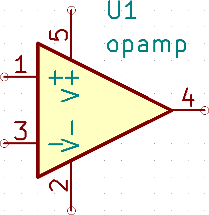
To match the symbol pins to the Spice model nodes shown above, one needs to use an alternate node sequence option with value: "1 3 5 2 4". It is a list of pin numbers corresponding to the Spice model nodes order. |
Pasivo
Passive tab allows the user to assign a passive device model (resistor, capacitor or inductor) to a component. It is a rarely used option, as normally passive components have models assigned implicitly, unless component reference does not match the actual device type.
| Explicitly defined passive device models have priority over the ones assigned implicitly. It means that once a passive device model is assigned, the reference and value fields are not taken into account during simulation. It may lead to a confusing situation when assigned model value does not match the one displayed on a schematic sheet. |
Type |
Selects the device type (resistor, capacitor or inductor). |
Value |
Defines the device property (resistance, capacitance or inductance). The value may use common Spice unit prefixes (as listed below the text input field) and should use point as the decimal separator. Note that Spice does not correctly interpret prefixes intertwined in the value (e.g. 1k5). |
Model
Model tab is used to assign a semiconductor or a complex model defined in an external library file. Spice model libraries are often offered by device manufacturers.
The main text widget displays the selected library file contents. It is a common practice to put models description inside library files, including the node order.
File |
Path to a Spice library file. This file is going to be used by the simulator, as it is added using .include directive. |
Model |
Selected device model. When a file is selected, the list is filled with available models to choose from. |
Type |
Selects model type (subcircuit, BJT, MOSFET or diode). Normally it is set automatically when a model is selected. |
Source
Source tab is used to assign a power or signal source model. There are two sections: DC/AC analysis and Transient analysis. Each defines source parameters for the corresponding simulation type.
Source type option applies to all simulation types.
Refer to the ngspice documentation, chapter 4 (Voltage and Current Sources) for more details about sources.
Spice directives
It is possible to add Spice directives by placing them in text fields on a schematic sheet. This approach is convenient for defining the default simulation type. This functionality is limited to Spice directives starting with a dot (e.g. ".tran 10n 1m"), it is not possible to place additional components using text fields.
Simulation
To launch a simulation, open Spice Simulator dialog by selecting menu Tools→Simulator in the schematics editor window.
The dialog is divided into several sections:
Menu
File
New Plot |
Create a new tab in the plot panel. |
Open Workbook |
Open a list of plotted signals. |
Save Workbook |
Save a list of plotted signals. |
Save as image |
Export the active plot to a .png file. |
Save as .csv file |
Export the active plot raw data points to a .csv file. |
Exit Simulation |
Close the dialog. |
Simulation
Run Simulation |
Perform a simulation using the current settings. |
Add signals… |
Open a dialog to select signals to be plotted. |
Probe from schematics |
Start the schematics Probe tool. |
Tune component value |
Start the Tuner tool. |
Show SPICE Netlist… |
Open a dialog showing the generated netlist for the simulated circuit. |
Settings… |
Open the simulation settings dialog. |
View
Zoom In |
Zoom in the active plot. |
Zoom Out |
Zoom out the active plot. |
Fit on Screen |
Adjust the zoom setting to display all plots. |
Show grid |
Toggle grid visibility. |
Show legend |
Toggle plot legend visibility. |
Toolbar
The top toolbar provides access to the most frequently performed actions.
Run/Stop Simulation |
Start or stop the simulation. |
Add Signals |
Open a dialog to select signals to be plotted. |
Probe |
Start the schematics Probe tool. |
Tune |
Start the Tuner tool. |
Settings |
Open the simulation settings dialog. |
Plot panel
Visualizes the simulation results as plots. One can have multiple plots opened in separate tabs, but only the active one is updated when a simulation is executed. This way it is possible to compare simulation results for different runs.
Plots might be customized by toggling grid and legend visibility using View menu. When a legend is visible, it can be dragged to change its position.
Plot panel interaction:
-
scroll mouse wheel to zoom in/out
-
right click to open a context menu to adjust the view
-
draw a selection rectangle to zoom in the selected area
-
drag a cursor to change its coordinates
Output console
Output console displays messages from the simulator. It is advised to check the console output to verify there are no errors or warnings.
Signals list
Shows the list of signals displayed in the active plot.
Signals list interaction:
-
right click to open a context menu to hide signal or toggle cursor
-
double click to hide signal
Cursors list
Shows the list of cursors and their coordinates. Each signal may have one cursor displayed. Cursors visibility is set using the Signals list.
Tune panel
Displays components picked with the Tuner tool. Tune panel allows the user to quickly modify component values and observe their influence on the simulation results - every time a component value is changed, the simulation is rerun and plots are updated.
For each component there a few controls associated:
-
The top text field sets the maximum component value.
-
The middle text field sets the actual component value.
-
The bottom text field sets the minimum component value.
-
Slider allows the user to modify the component value in a smooth way.
-
Save button modifies component value on the schematics to the one selected with the slider.
-
X button removes component from the Tune panel and restores its original value.
The three text fields recognize Spice unit prefixes.
Tuner tool
Tuner tool lets the user pick components for tuning.
To select a component for tuning, click on one in the schematics editor when the tool is active. Selected components will appear in the Tune panel. Only passive components might be tuned.
Probe tool
Probe tool provides an user-friendly way of selecting signals for plotting.
To add a signal to plot, click on a corresponding wire in the schematics editor when the tool is active.
Simulation settings
Simulation settings dialog lets the user set the simulation type and parameters. There are four tabs:
-
AC
-
DC Transfer
-
Transient
-
Custom
The first three tabs provide forms where simulation parameters might be specified. The last tab allows the user to type in custom Spice directives to set up a simulation. You can find more information about simulation types and parameters in the ngspice documentation, chapter 1.2.
An alternative way to configure a simulation is to type Spice directives into text fields on schematics. Any text field directives related to simulation type are overridden by the settings selected in the dialog. It means that once you start using the simulation dialog, the dialog overriddes the schematics directives until the simulator is reopened.
There are two options common to all simulation types:
Adjust passive symbol values |
Replace passive symbol values to convert common component values notation to Spice notation. |
Add full path for .include library directives |
Prepend Spice model library file names with full path. Normally full path is required by ngspice to access a library file. |