Manuel de référence
Copyright
This document is Copyright © 2010-2018 by its contributors as listed below. You may distribute it and/or modify it under the terms of either the GNU General Public License (http://www.gnu.org/licenses/gpl.html), version 3 or later, or the Creative Commons Attribution License (http://creativecommons.org/licenses/by/3.0/), version 3.0 or later.
Toutes les marques apparaissant dans ce document appartiennent à leurs propriétaires respectifs.
Contributeurs
Jean-Pierre Charras, Fabrizio Tappero, Marc Berlioux.
Traduction
Marc Berlioux <[email protected]>, 2015-2016
Retours
Merci de signaler vos corrections de bugs, suggestions ou nouvelles versions ici :
-
Documentation de KiCad : https://gitlab.com/kicad/services/kicad-doc/issues
-
Bugs logiciel KiCad : https://gitlab.com/kicad/code/kicad/issues
-
About KiCad translation: https://gitlab.com/kicad/code/kicad-i18n/issues
Date de publication et version du logiciel
Published on May 30, 2015.
Introduction à Eeschema
Description
Eeschema is a schematic capture software distributed as a part of KiCad and available under the following operating systems:
-
Linux
-
Apple macOS
-
Windows
Les fichiers de Eeschema sont compatibles d’un système d’exploitation à un autre.
Eeschema est une application intégrée à partir de laquelle toutes les fonctions de dessin, de contrôle, de mise en page, de gestion des librairies et d’accès au logiciel de conception de circuit imprimé sont accessibles.
Eeschema is intended to cooperate with PcbNew, which is KiCad’s printed circuit design software. It can also export netlist files, which lists all the electrical connections, for other packages.
Eeschema includes a symbol library editor, which can create and edit symbols and manage libraries. It also integrates the following additional but essential functions needed for modern schematic capture software:
-
La vérification des règles électriques ou ERC (Electrical Rules Check), pour le contrôle des connexions manquantes ou incorrectes.
-
L’exportation de fichiers de tracé en plusieurs formats (Postscript, PDF, HPGL, SVG)
-
Bill of Materials generation (via Python or XSLT scripts, which allow many flexible formats).
Aperçu technique
Eeschema is limited only by the available memory. There is thus no real limitation to the number of components, component pins, connections or sheets. In the case of multi-sheet diagrams, the representation is hierarchical.
Eeschema can use multi-sheet diagrams in a few ways:
-
Schémas à hiérarchie simple (chaque schéma n’est utilisé qu’une fois).
-
Schémas à hiérarchie complexe (certains schémas sont utilisés plus d’une fois, en plusieurs instances).
-
Schémas à hiérarchie plate (les schémas ne font pas explicitement partie d’un schéma maître).
Commandes de bases de Eeschema
Commands can be executed by:
-
En cliquant sur les menus, en haut de la fenêtre.
-
En cliquant sur les boutons de la barre d’outil principale, au sommet de la fenêtre, sous les menus.
-
En cliquant sur les boutons de la barre d’outils à droite de la fenêtre (outils de placement d’éléments).
-
En cliquant sur les boutons de la barre d’outils à gauche de la fenêtre (options d’affichage).
-
En utilisant la souris (commandes complémentaires importantes), notamment au moyen du clic droit sur un élément du schéma, qui affiche un menu contextuel (options de zoom, de dimension de grille et d’édition des éléments).
-
Function keys (F1, F2, F3, F4, Insert and Space keys). Specifically: Escape key cancels the command in progress. Insert key allows the duplication of the last element created.
-
Pressing hot keys which typically perform a select tool command and begin tool action at the current cursor location. For a list of hot keys, see the "Help→List Hotkeys" menu entry or press 'Ctrl+F1' key.
Commandes à la souris
Commandes de base
Bouton gauche
-
Single click: displays the characteristics of the symbol or text under the cursor in the status bar.
-
Double click: edit (if the element is editable) the symbol or text.
Bouton droit
-
Ouvre un menu contextuel, en fonction de l’élément sous le curseur.
Block operations
Vous pouvez déplacer, traîner ou détruire des zones sélectionnées dans tous les modes de Eeschema. La différence entre 'déplacer' (Move) et 'traîner' (Drag) est que les liaisons électriques entre éléments sont conservées lors d’un Drag.
Areas are selected by drawing a box around items using the left mouse button.
Holding Shift'', Ctrl'', or ``Shift + Ctrl'' during selection respectively performs copying, dragging and deletion:
Bouton gauche de la souris |
Déplacer la sélection (Move). |
Shift + bouton gauche de la souris |
Copier la sélection. |
Ctrl + bouton gauche de la souris |
Traîner la sélection (Drag). |
Ctrl + Shift + bouton gauche de la souris |
Supprimer la sélection. |
Lors d’un "drag" ou d’une copie, vous pouvez :
-
Cliquer à nouveau du bouton gauche pour poser les éléments.
-
Click the right button or press Escape key to cancel.
If a block move command has started, another command can be selected using the right-click pop-up menu.
Raccourcis clavier
-
L’appui sur la touche [Ctrl+F1] affiche la liste des raccourcis clavier.
-
Hotkeys might be redefined in Controls tab of Schematic Editor Options dialog (menu Preferences → General Options).
Here is the default hotkey list:
Help (this window) |
Ctrl+F1 |
Zoom In |
F1 |
Zoom Out |
F2 |
Zoom Redraw |
F3 |
Zoom Center |
F4 |
Fit on Screen |
Home |
Zoom to Selection |
@ |
Reset Local Coordinates |
Space |
Edit Item |
E |
Delete Item |
Del |
Rotate Item |
R |
Drag Item |
G |
Undo |
Ctrl+Z |
Redo |
Ctrl+Y |
Mouse Left Click |
Return |
Mouse Left Double Click |
End |
Save Schematic |
Ctrl+S |
Load Schematic |
Ctrl+O |
Find Item |
Ctrl+F |
Find Next Item |
F5 |
Find Next DRC Marker |
Shift+F5 |
Find and Replace |
Ctrl+Alt+F |
Repeat Last Item |
Ins |
Move Block → Drag Block |
Tab |
Copy Block |
Ctrl+C |
Paste Block |
Ctrl+V |
Cut Block |
Ctrl+X |
Move Schematic Item |
M |
Duplicate Symbol or Label |
C |
Add Symbol |
A |
Add Power |
P |
Mirror X |
X |
Mirror Y |
Y |
Orient Normal Symbol |
N |
Edit Symbol Value |
V |
Edit Symbol Reference |
U |
Edit Symbol Footprint |
F |
Edit with Symbol Editor |
Ctrl+E |
Begin Wire |
W |
Begin Bus |
B |
End Line Wire Bus |
K |
Add Label |
L |
Add Hierarchical Label |
H |
Add Global Label |
Ctrl+L |
Add Junction |
J |
Add No Connect Flag |
Q |
Add Sheet |
S |
Add Wire Entry |
Z |
Add Bus Entry |
/ |
Add Graphic PolyLine |
I |
Add Graphic Text |
T |
Update PCB from Schematic |
F8 |
Autoplace Fields |
O |
Leave Sheet |
Alt+BkSp |
Delete Node |
BkSp |
Highlight Connection |
Ctrl+X |
All hotkeys can be redefined using the hotkey editor (menu Preferences→General Options→Controls).
It is possible to import/export hotkey settings using menu Preferences→Import and Export→Import/Export Hotkeys.
Grid
In Eeschema the cursor always moves over a grid. The grid can be customized:
-
Size might be changed using the pop-up menu or using the Preferences/Options menu.
-
Color might be changed in Colors tab of the Schematic Editor Options dialog (menu Preferences → General Options).
-
Visibility might be switched using the left-hand toolbar button.
La taille par défaut de la grille est de 50 mils (0.050") soit 1.27 mm.
This is the preferred grid to place symbols and wires in a schematic, and to place pins when designing a symbol in the Symbol Editor.
One can also work with a smaller grid from 25 mil to 10 mil. This is only intended for designing the symbol body or placing text and comments and not recommended for placing pins and wires.
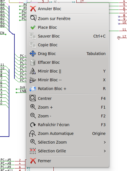
Sélection du Zoom
Pour changer le niveau du zoom :
-
Cliquez du bouton droit pour ouvrir le menu contextuel et choisissez la valeur de zoom désirée.
-
Ou utilisez les touches de fonctions :
-
F1: Zoom in
-
F2: Zoom out
-
F4 or simply click on the middle mouse button (without moving the mouse): Center the view around the cursor pointer position
-
-
Zoom fenêtre :
-
Mouse wheel: Zoom in/out
-
Shift+Mouse wheel: Pan up/down
-
Ctrl+Mouse wheel: Pan left/right
-
Affichage des coordonnées du curseur
The display units are in inches or millimeters. However, Eeschema always uses 0.001 inch (mil/thou) as its internal unit.
Les informations suivantes sont affichées en bas et à droite de la fenêtre :
-
Le facteur de Zoom
-
La position absolue du curseur (X Y)
-
La position relative du curseur (dx dy)
The relative coordinates can be reset to zero by pressing Space. This is useful for measuring distance between two points or aligning objects.

Barre de menu
The top menu bar allows the opening and saving of schematics, program configuration and viewing the documentation.

Barre d’outils supérieure
Cette barre d’outils donne accès aux principales fonctions de Eeschema.
Si Eeschema est lancé tout seul (mode standalone), et non par le gestionnaire de projets, voici les boutons disponibles :

Note that when KiCad runs in project mode, the first two icons are not available as they work with individual files.
|
Create a new schematic (only in standalone mode). |
|
Open a schematic (only in standalone mode). |
|
Save complete schematic project. |
|
Select the sheet size and edit the title block. |
|
Open print dialog. |
|
Paste a copied/cut item or block to the current sheet. |
|
Undo: Revert the last change. |
|
Redo: Revert the last undo operation. |
|
Show the dialog to search symbols and texts in the schematic. |
|
Show the dialog to search and replace texts in the schematic. |
|
Refresh screen; zoom to fit. |
|
Zoom in and out. |
|
View and navigate the hierarchy tree. |
|
Leave the current sheet and go up in the hierarchy. |
|
Call the symbol library editor to view and modify libraries and symbols. |
|
Browse symbol libraries. |
|
Annotate symbols. |
|
Electrical Rules Checker (ERC), automatically validate electrical connections. |
|
Call CvPcb to assign footprints to symbols. |
|
Export a netlist (Pcbnew, SPICE and other formats). |
|
Edit symbol fields. |
|
Generate the Bill of Materials (BOM). |
|
Call Pcbnew to perform a PCB layout. |
|
Back-import footprint assignment (selected using CvPcb or Pcbnew) into the "footprint" fields. |
Barre d’outils latérale droite
Cette barre d’outils contient les outils pour :
-
Place symbols, wires, buses, junctions, labels, text, etc.
-
Create hierarchical subsheets and connection symbols.
|
Cancel the active command or tool. |
|
Highlight a net by marking its wires and net labels with a different color. If KiCad runs in project mode then copper corresponding to the selected net will be highlighted in Pcbnew as well. |
|
Display the symbol selector dialog to select a new symbol to be placed. |
|
Display the power symbol selector dialog to select a power symbol to be placed. |
|
Draw a wire. |
|
Draw a bus. |
|
Draw wire-to-bus entry points. These elements are only graphical and do not create a connection, thus they should not be used to connect wires together. |
|
Draw bus-to-bus entry points. |
|
Place a "No Connect" flag. These flags should be placed on symbol pins which are meant to be left unconnected. It is done to notify the Electrical Rules Checker that lack of connection for a particular pin is intentional and should not be reported. |
|
Place a junction. This connects two crossing wires or a wire and a pin, when it can be ambiguous (i.e. if a wire end or a pin is not directly connected to another wire end). |
|
Place a local label. Local label connects items located in the same sheet. For connections between two different sheets, you have to use global or hierarchical labels. |
|
Place a global label. All global labels with the same name are connected, even when located on different sheets. |
|
Place a hierarchical label. Hierarchical labels are used to create a connection between a subsheet and the parent sheet that contains it. |
|
Place a hierarchical subsheet. You must specify the file name for this subsheet. |
|
Import a hierarchical pin from a subsheet. This command can be executed only on hierarchical subsheets. It will create hierarchical pins corresponding to hierarchical labels placed in the target subsheet. |
|
Place a hierarchical pin in a subsheet. This command can be executed only on hierarchical subsheets. It will create arbitrary hierarchical pins, even if they do not exist in the target subsheet. |
|
Draw a line. These are only graphical and do not connect anything. |
|
Place a text comment. |
|
Place a bitmap image. |
|
Delete selected element. |
Barre d’outils latérale gauche
Cette barre d’outils permet de gérer les options d’affichage :
|
Toggle grid visibility. |
|
Switch units to inches. |
|
Switch units to millimeters. |
|
Choose the cursor shape (full screen/small). |
|
Toggle visibility of "invisible" pins. |
|
Toggle free angle/90 degrees wires and buses placement. |
Menus contextuels et édition rapide
Un clic droit ouvre un menu contextuel pour l’élément sélectionné ou survolé : ce menu permet d’ajuster :
-
Le facteur de Zoom.
-
La taille de grille.
-
Les paramètres couramment édités de l’élément sélectionné.
Menu contextuel en dehors d’un élément.
Editing a label.
Editing a symbol.
Barre de menus
Menu Fichiers
| New | Close current schematic and start a new one (only in standalone mode). |
|---|---|
Open |
Load a schematic project (only in standalone mode). |
Open Recent |
Open a schematic project from the list of recently opened files (only in standalone mode). |
Append Schematic Sheet |
Insert the contents of another sheet into the current one. |
Import Non-Kicad Schematic File |
Imports a schematic project saved in another file format. |
Save |
Save current sheet and all its subsheets. |
Save Current Sheet |
Save only the current sheet, but not others in the project. |
Save Current Sheet As… |
Save the current sheet under a new name. |
Page Settings |
Configure page dimensions and title block. |
Print schematic project (See also chapter Plot and Print). |
|
Plot |
Export to PDF, PostScript, HPGL or SVG format (See chapter Plot and Print). |
Close |
Terminate the application. |
Menu Préférences
Manage Symbol Library Tables |
Add/remove symbol libraries. |
Configure Paths |
Set the default search paths. |
General Options |
Preferences (units, grid size, field names, etc.). |
Set Language |
Select interface language. |
Icons Options |
Icons visibility settings. |
Import and Export |
Transfer preferences to/from file. |
Manage Symbol Library Tables
Eeschema uses two library tables to store the list of available symbol libraries, which differ by the scope:
-
Global Libraries
Libraries listed in the Global Libraries table are available to every project. They are saved in sym-lib-table in your home directory (exact path is dependent on the operating system; check the path above the table).
-
Project Specific Libraries
Libraries listed in Project Specific Libraries table are available to the currently opened project. They are saved in sym-lib-table file in the project directory (check the path above the table).
You can view either list by clicking on "Global Libraries" or "Project Specific Libraries" tab below the library table.
Add a new library
Add a library either by clicking Browse Libraries… button and selecting a file or clicking "Append Library" and typing a path to a library file. The selected library will be added to the currently opened library table (Global/Project Specific).
Remove a library
Remove a library by selecting one or more libraries and clicking Remove Library button.
Library properties
Each row in the table stores several fields describing a library:
Active |
Enables/disables the library. It is useful to temporarily reduce the loaded library set. |
Nickname |
Nickname is a short, unique identifier used for assigning symbols to components. Symbols are represented by '<Library Nickname>:<Symbol Name>' strings. |
Library Path |
Path points to the library location. |
Plugin Type |
Determines the library file format. |
Options |
Stores library specific options, if used by plugin. |
Description |
Briefly characterizes the library contents. |
General Options
Display
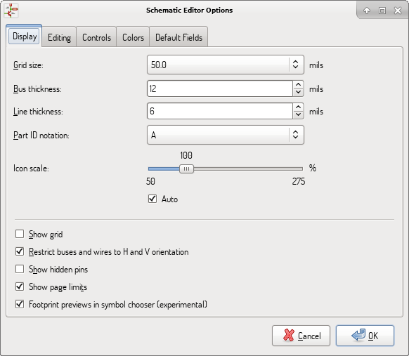
Grid Size |
Grid size selection. It is recommended to work with normal grid (0.050 inches or 1,27 mm). Smaller grids are used for component building. |
Bus thickness |
Pen size used to draw buses. |
Line thickness |
Pen size used to draw objects that do not have a specified pen size. |
Part ID notation |
Style of suffix that is used to denote symbol units (U1A, U1.A, U1-1, etc.) |
Icon scale |
Adjust toolbar icons size. |
Show Grid |
Grid visibility setting. |
Restrict buses and wires to H and V orientation |
If checked, buses and wires are drawn only with vertical or horizontal lines. Otherwise buses and wires can be placed at any orientation. |
Show hidden pins: |
Display invisible (or hidden) pins, typically power pins. |
Show page limits |
If checked, shows the page boundaries on screen. |
Footprint previews in symbol chooser |
Displays a footprint preview frame and footprint selector when placing a new symbol. Note: it may cause problems or delays, use at your own risk. |
Editing
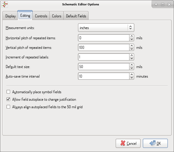
Measurement units |
Select the display and the cursor coordinate units (inches or millimeters). |
Horizontal pitch of repeated items |
Increment on X axis during element duplication (default: 0) (after placing an item like a symbol, label or wire, a duplication is made by the Insert key) |
Vertical pitch of repeated items |
Increment on Y axis during element duplication (default: 0.100 inches or 2,54 mm). |
Increment of repeated labels |
Increment of label value during duplication of texts ending in a number, such as bus members (usual value 1 or -1). |
Default text size |
Text size used when creating new text items or labels. |
Auto-save time interval |
Time in minutes between saving backups. |
Automatically place symbol fields |
If checked, symbol fields (e.g. value and reference) in newly placed symbols might be moved to avoid collisions with other items. |
Allow field autoplace to change justification |
Extension of 'Automatically place symbol fields' option. Enable text justification adjustment for symbol fields when placing a new part. |
Always align autoplaced fields to the 50 mil grid |
Extension of 'Automatically place symbol fields' option. If checked, fields are autoplaced using 50 mils grid, otherwise they are placed freely. |
Controls
Redefine hotkeys and set up the user interface behavior.
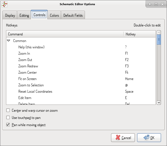
Select a new hotkey by double clicking an action or right click on an action to show a popup menu:
Edit |
Define a new hotkey for the action (same as double click). |
Undo Changes |
Reverts the recent hotkey changes for the action. |
Restore Default |
Sets the action hotkey to its default value. |
Undo All Changes |
Reverts all recent hotkey changes for the action. |
Restore All to Default |
Sets all action hotkeys to their default values. |
Options description:
Center and warp cursor on zoom |
If checked, the pointed location is warped to the screen center when zooming in/out. |
Use touchpad to pan |
When enabled, view is panned using scroll wheels (or touchpad gestures) and to zoom one needs to hold Ctrl. Otherwise scroll wheels zoom in/out and Ctrl/Shift are the panning modifiers. |
Pan while moving object |
If checked, automatically pans the window if the cursor leaves the window during drawing or moving. |
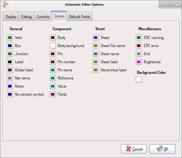
Colors
Color scheme for various graphic elements. Click on any of the color swatches to select a new color for a particular element.
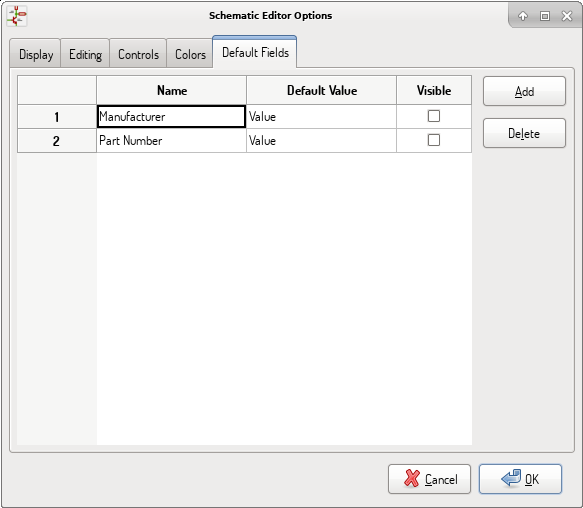
Default Fields
Define additional custom fields and corresponding values that will appear in newly placed symbols.
Menu Aide
Access to on-line help (this document) for an extensive tutorial about KiCad.
Use ``Copy Version Information'' when submitting bug reports to identify your build and system.
Barre d’outils principale
Gestion des feuilles schématiques
The Sheet Settings icon (![]() ) allows you to define the sheet size and the contents of the title block.
) allows you to define the sheet size and the contents of the title block.
Le nombre de feuilles, numéro de feuille, sont mis à jour automatiquement. La date ne sera pas changée automatiquement, mais vous pouvez la fixer à aujourd’hui en cliquant sur le bouton "←".
Outil de recherche
The Find icon (![]() ) can be used to access the search tool.
) can be used to access the search tool.
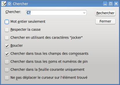
You can search for a reference, a value or a text string in the current sheet or in the whole hierarchy. Once found, the cursor will be positioned on the found element in the relevant sub-sheet.
Outil de Netliste
The Netlist icon (![]() ) opens the netlist generation tool.
) opens the netlist generation tool.
The tool creates a file which describe all connections in the entire hierarchy.
In a multisheet hierarchy, any local label is visible only inside the sheet to which it belongs. For example: the label LABEL1 of sheet 3 is different from the label LABEL1 of sheet 5 (if no connection has been intentionally introduced to connect them). This is due to the fact that the sheet name path is internally associated with the local label.
| Even though there is no text length limit for labels in Eeschema, please take into account that other programs reading the generated netlist may have such constraints. |
| Avoid spaces in labels, because they will appear as separated words in the generated file. It is not a limitation of Eeschema, but of many netlist formats, which often assume that a label has no spaces. |
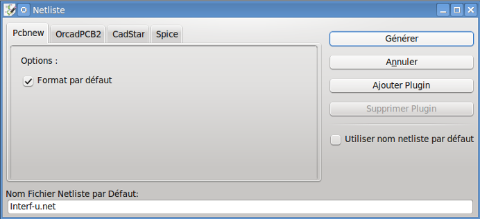
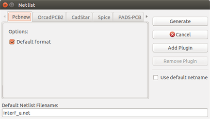
Options :
Default Format |
Check to select Pcbnew as the default format. |
D’autres formats de netlistes peuvent être générés :
-
Orcad PCB2
-
CadStar
-
Spice (simulators)
External plugins can be added to extend the netlist formats list (PadsPcb Plugin was added in the picture above).
There is more information about creating netlists in Create a Netlist chapter.
Outil d’annotation
The icon ![]() launches the annotation tool. This tool assigns references to components.
launches the annotation tool. This tool assigns references to components.
Pour des composants multi-unités (comme par exemple le 7400 qui contient 4 portes), un suffixe d’unité sera attribué (ainsi notre 7400 désigné par la référence U3 sera divisé en quatre unités référencées U3A, U3B, U3C et U3D).
You can unconditionally annotate all the components or only the new components, i.e. those which were not previously annotated.
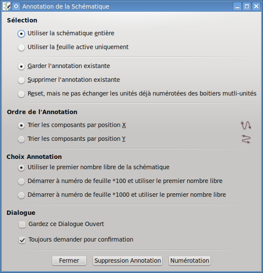
Portée
| Use the entire schematic | All sheets are re-annotated (default). |
|---|---|
Use the current page only |
Only the current sheet is re-annotated (this option is to be used only in special cases, for example to evaluate the amount of resistors in the current sheet.). |
Keep existing annotation |
Conditional annotation, only the new components will be re-annotated (default). |
Reset existing annotation |
Unconditional annotation, all the components will be re-annotated (this option is to be used when there are duplicated references). |
Reset, but do not swap any annotated multi-unit parts |
Keeps all groups of multiple units (e.g. U2A, U2B) together when reannotating. |
Ordre d’annotation
Selects the order in which components will be numbered (either horizontally or vertically).
Choix de l’annotation
Selects the assigned reference format.
Outil de vérification des règles électriques
The icon ![]() launches the electrical rules check (ERC) tool.
launches the electrical rules check (ERC) tool.
This tool performs a design verification and is able to detect forgotten connections, and inconsistencies.
Once you have run the ERC, Eeschema places markers to highlight problems. The error description is displayed after left clicking on the marker. An error report file can also be generated.
Fenêtre principale de l’ERC
Errors are displayed in the Electrical Rules Checker dialog:
-
Total : nombre total d’erreurs et avertissements.
-
Erreurs : nombre d’erreurs.
-
Warnings : nombre d’avertissements.
Options :
Create ERC file report |
Check this option to generate an ERC report file. |
Commandes :
Delete Markers |
Remove all ERC error/warnings markers. |
Run |
Start an Electrical Rules Check. |
Close |
Close the dialog. |
-
En cliquant sur une erreur, vous êtes emmenés au marqueur correspondant sur le schéma.
Options de l’ERC
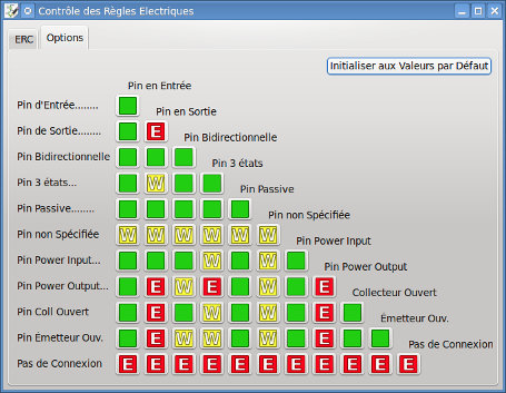
This tab allows you to define the connectivity rules between pins; you can choose between 3 options for each case:
-
Pas d’erreur (Vert)
-
Avertissement (W jaune)
-
Erreur (E rouge)
Chaque carré de la matrice peut être modifié en cliquant une ou plusieurs fois dessus.
Options :
Test similar labels |
Report labels that differ only by letter case (e.g. label/Label/LaBeL). Net names are case-sensitive therefore such labels are treated as separate nets. |
Test unique global labels |
Report global lables that occur only once for a particular net. Normally it is required to have at least two make a connection. |
Commandes :
Initialize to Default |
Restores the original settings. |
Outil de Liste de Matériel
The icon ![]() launches the bill of materials (BOM) generator. This tool generates a file listing the components and/or hierarchical connections (global labels).
launches the bill of materials (BOM) generator. This tool generates a file listing the components and/or hierarchical connections (global labels).
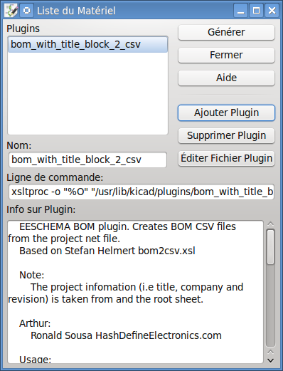
Eeschema’s BOM generator makes use of external plugins, either as XSLT or Python scripts. There are a few examples installed inside the KiCad program files directory.
Quelques champs de composants utiles à utiliser pour le BOM :
-
Valeur : nom unique pour chaque composant utilisé.
-
Empreinte : entrée soit manuellement, soit par rétro-annotation (voir ci-dessous).
-
Champ 1 : nom du fabricant.
-
Champ 2 : référence fabricant.
-
Champ 3 : référence distributeur.
Exemple :
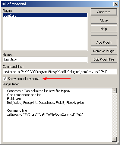
On MS Windows, BOM generator dialog has a special option (pointed by red arrow) that controls visibility of external plugin window. + By default, BOM generator command is executed console window hidden and output is redirected to Plugin info field. Set this option to show the window of the running command. It may be necessary if plugin has provides a graphical user interface.
Edit Fields tool
The icon ![]() opens a spreadsheet to view and modify field values for all symbols.
opens a spreadsheet to view and modify field values for all symbols.
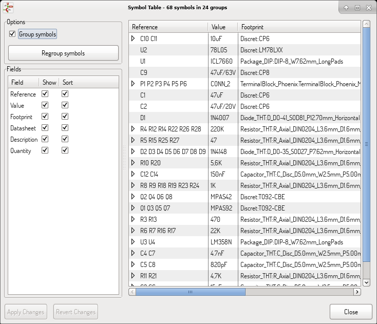
Once you modify field values, you need to either accept changes by clicking on 'Apply' button or undo them by clicking on 'Revert' button.
Tricks to simplify fields filling
There are several special copy/paste methods in spreadsheet. They may be useful when entering field values that are repeated in a few components.
These methods are illustrated below.
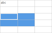
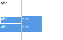
| Copy (Ctrl+C) | Selection | Paste (Ctrl+V) |
|---|---|---|
|
|
|
|
|
|
|
|
|
|
|
|
|
|
|
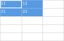
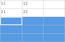
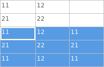
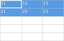
| These techniques are also available in other dialogs with a grid control element. |
Import tool for footprint assignment
Accès :
The icon ![]() launches the back-annotate tool.
launches the back-annotate tool.
Cet outil permet de rétro-importer les noms des empreintes choisies dans Pcbnew dans les champs empreintes de Eeschema.
Manage Symbol Libraries
Symbol libraries hold collections of symbols used when creating schematics. Each symbol in a schematic is uniquely identified by a full name that is composed of a library nickname and a symbol name. An example is Audio:AD1853.
Symbol Library Table
The symbol library table holds a list of all library files KiCad knows about. The symbol library table is constructed from the global symbol library table file and the project specific symbol library table file.
When a symbol is loaded, Eeschema uses the library nickname, Audio in our example, to lookup the library location in the symbol library table.
The image below shows the symbol library table editing dialog which can be opened by invoking the Manage Symbol Library Tables'' entry in the Preferences'' menu.
Global Symbol Library Table
The global symbol library table contains the list of libraries that are always available regardless of the currently loaded project file. The table is saved in the file sym-lib-table in the user’s home folder. The location of this folder is dependent upon the operating system being used.
Project Specific Symbol Library Table
The project specific symbol library table contains the list of libraries that are available specifically for the currently loaded project file. The project specific symbol library table can only be edited when it is loaded along with the project file. If no project file is loaded or there is no symbol library table file in the current project path, an empty table is created which can be edited and later saved along with the project file.
Initial Configuration
The first time Eeschema is run and the global symbol table file sym-lib-table is not found in the user’s home folder, Eeschema will attempt to copy the default symbol table file sym-lib-table stored in the system’s KiCad template folder to the file sym-lib-table in the user’s home folder. If the default template sym-lib-table file cannot be found, a dialog will prompt for an alternate location for the sym-lib-table file. If no sym-lib-table is found or the dialog is dismissed, an empty symbol library table will be created in the user’s home folder. If this happens, the user can either copy sym-lib-table manually or configure the table by hand.
|
The default symbol library table includes all of the symbol libraries that are installed as part of KiCad. This may or may not be desirable depending on usages and the speed of the system. The amount of time required to load the symbol libraries is proportional to the number of libraries in the symbol library table. If symbol library load times are excessive, remove rarely and/or never used libraries from the global library table and add them to the project library table as required. |
Adding Table Entries
In order to use a symbol library, it must first be added to either the global table or the project specific table. The project specific table is only applicable when you have a project file open.
Each library entry must have a unique nickname.
This does not have to be related in any way to the actual library file name or path. The colon ':' and '/' characters cannot be used anywhere in the library nickname. Each library entry must have a valid path and/or file name depending on the type of library. Paths can be defined as absolute, relative, or by environment variable substitution (see section below).
The appropriate plug in type must be selected in order for the library to be properly read. KiCad currently supports only legacy symbol library files plug-in.
There is also a description field to add a description of the library entry. The option field is not used at this time so adding options will have no effect when loading libraries.
-
Please note that you cannot have duplicate library nicknames in the same table. However, you can have duplicate library nicknames in both the global and project specific symbol library table.
-
The project specific table entry will take precedence over the global table entry when duplicate nicknames occur.
-
When entries are defined in the project specific table, a sym-lib-table file containing the entries will be written into the folder of the currently open project file.
Environment Variable Substitution
One of the most powerful features of the symbol library table is environment variable substitution. This allows for definition of custom paths to where symbol libraries are stored in environment variables. Environment variable substitution is supported by using the syntax $\{ENV_VAR_NAME\} in the library path.
By default, at run time KiCad defines two environment variables:
-
the KIPRJMOD environment variable that always points to the currently open project directory. KIPRJMOD cannot be modified.
-
the KICAD_SYMBOL_DIR environment variable. This points to the path where the default symbol libraries that were installed with KiCad.
You can override KICAD_SYMBOL_DIR by defining it yourself in preferences/ Configure Path which allows you to substitute your own libraries in place of the default KiCad symbol libraries.
KIPRJMOD allows you to store libraries in the project path without having to define the absolute path (which is not always known) to the library in the project specific symbol library table.
Usage Patterns
Symbol libraries can be defined either globally or specifically to the currently loaded project. Symbol libraries defined in the user’s global table are always available and are stored in the sym-lib-table file in the user’s home folder. The project specific symbol library table is active only for the currently open project file.
There are advantages and disadvantages to each method. Defining all libraries in the global table means they will always be available when needed. The disadvantage of this is that load time will increase.
Defining all symbol libraries on a project specific basis means that you only have the libraries required for the project which decreases symbol library load times. The disadvantage is that you always have to remember to add each symbol library that you need for every project.
One usage pattern would be to define commonly used libraries globally and the libraries only required for the project in the project specific library table. There is no restriction on how to define libraries.
Legacy Project Remapping
When loading a schematic created prior to the symbol library table implementation, Eeschema will attempt to remap the symbol library links in the schematic to the appropriate library table symbols. The success of this process is dependent on several factors:
-
the original libraries used in the schematic are still available and unchanged from when the symbol was added to the schematic.
-
all rescue operations were performed when detected to create a rescue library or keep the existing rescue library up to date.
-
the integrity of the project symbol cache library has not been corrupted.
|
The remapping will make a back up of all the files that are changed during remapping in the rescue-backup folder in the project folder. Always make a back up of your project before remapping just in case something goes wrong. |
|
The rescue operation is performed even if it has been disabled to ensure the correct symbols are available for remapping. Do not cancel this operation or the remapping will fail to correctly remap schematics symbols. Any broken symbol links will have to be fixed manually. |
|
If the original libraries have been removed and the rescue was not performed, the cache library can be used as a recovery library as a last resort. Copy the cache library to a new file name and add the new library file to the top of the library list using a version of Eeschema prior to the symbol library table implementation. |
Création et édition de schémas
Introduction
Un schéma peut être représenté sur une seule feuille, mais, s’il est assez grand, il lui faudra plusieurs feuilles.
Un schéma représenté sur plusieurs feuilles est un schéma hiérarchique, et toutes ses feuilles (chacune représentée par son propre fichier) constituent un projet Eeschema. La manipulation des schémas hiérarchiques sera décrite au chapitre Schématiques hiérarchiques .
Généralités
Un schéma conçu avec Eeschema est plus que la simple représentation graphique d’un dispositif électronique. Il est normalement le point d’entrée d’une chaîne de développement qui permet de :
-
Valider un ensemble de règles (Vérification des règles électriques (ERC)) pour détecter les erreurs et omissions.
-
Générer automatiquement une liste de composants (BOM).
-
Générer une netliste pour des logiciels de simulation, comme SPICE.
-
Générer une netliste pour la transférer à un logiciel de dessin de circuit imprimé.
A schematic mainly consists of symbols, wires, labels, junctions, buses and power ports. For clarity in the schematic, you can place purely graphical elements like bus entries, comments, and polylines.
Chaîne de développement
Symbols are added to the schematic from symbol libraries. After the schematic is made, a netlist is generated, which is later used to import the set of connections and footprints into PcbNew.
Symbol placement and editing
Find and place a symbol
To load a symbol into your schematic you can use the icon ![]() . A dialog box allows you to type the name of the symbol to load.
. A dialog box allows you to type the name of the symbol to load.
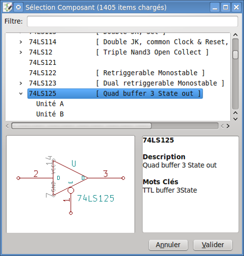
The Choose Symbols dialog will filter symbols by name, keywords, and description according to what you type into the search field. Advanced filters can be used just by typing them:
-
Wildcards: use the characters
?and*respectively to mean "any character" and "any number of characters". -
Relational: if a library part’s description or keywords contain a tag of the format "Key:123", you can match relative to that by typing "Key>123" (greater than), "Key<123" (less than), etc. Numbers may include one of the following case-insensitive suffixes:
p
n
u
m
k
meg
g
t
10-12
10-9
10-6
10-3
103
106
109
1012
ki
mi
gi
ti
210
220
230
240
-
Regular expression: if you’re familiar with regular expressions, these can be used too. The regular expression flavor used is the wxWidgets Advanced Regular Expression style, which is similar to Perl regular expressions.
Before placing the symbol in the schematic, you can rotate it, mirror it, and edit its fields, by either using the hotkeys or the right-click context menu. This can be done the same way after placement.
Here is a symbol during placement:
Alimentations
A power port symbol is a symbol (the symbols are grouped in the “power” library), so they can be placed using the symbol chooser. However, as power placements are frequent, the ![]() tool is available. This tool is similar, except that the search is done directly in the ``power'' library.
tool is available. This tool is similar, except that the search is done directly in the ``power'' library.
Symbol Editing and Modification (already placed component)
There are two ways to edit a symbol:
-
Modification of the symbol itself: position, orientation, unit selection on a multi-unit symbol.
-
Modification of one of the fields of the symbol: reference, value, footprint, etc.
When a symbol has just been placed, you may have to modify its value (particularly for resistors, capacitors, etc.), but it is useless to assign to it a reference number right away, or to select the unit (except for components with locked units, which you have to assign manually). This can be done automatically by the annotation function.
Symbol modification
To modify some feature of a symbol, position the cursor on the symbol, and then either:
-
Double-click on the symbol to open the full editing dialog.
-
Faites un clic droit pour ouvrir le menu contextuel et choisissez l’une des commandes : Déplacer, Orienter, Éditer, Supprimer, etc…
Édition des champs du composant
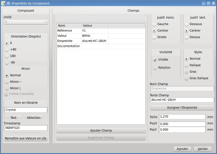
Vous pouvez modifier la référence, la valeur, la position, l’orientation, la taille du texte et la visibilité des champs :
-
Double-cliquez sur le champ à modifier.
-
Faites un clic droit pour ouvrir le menu contextuel et choisissez l’une des commandes : Déplacer, Orienter, Éditer, Supprimer, etc…
For more options, or in order to create fields, double-click on the symbol to open the Symbol Properties dialog.
Each field can be visible or hidden, and displayed horizontally or vertically. The displayed position is always indicated for a normally displayed symbol (no rotation or mirroring) and is relative to the anchor point of the symbol.
The option “Reset to Library Defaults” sets the symbol to the original orientation, and resets the options, size and position of each field. However, texts fields are not modified because this could break the schematic.
Fils, Bus, Labels, Alimentations
Introduction
Tous ces éléments peuvent être placés à partir des outils de la barre latérale droite
Ces éléments peuvent être des :
-
Wires: most connections between symbols.
-
Bus : pour relier graphiquement des labels de bus
-
Polygones : pour la présentation graphique.
-
Jonctions : pour créer des connexions au croisement de fils ou de bus.
-
Bus entries: to show connections between wires and buses.
-
Labels: pour étiqueter ou établir des connexions.
-
Labels globaux: pour établir des connexions entre feuilles.
-
Textes: pour ajouter des commentaires ou des notes.
-
Symboles de Non-Connexion: pour signaler une pin de composant qui ne sera pas utilisée.
-
Feuilles Hiérarchiques, et leurs pins de connexions.
Connexions (Fils et Labels)
Il y a deux moyens d’établir des connexions :
-
Fils de pin à pin.
-
Labels.
La figure ci-dessous montre les deux méthodes :
Note 1 :
Le point de "contact" d’un label est le coin inférieur gauche de la première lettre de l’étiquette. Ce point est affiché avec un petit carré lorsqu’il n’est pas connecté.
Ce point doit donc être en contact avec le fil, ou être superposé à l’extrémité d’une pin pour que le label soit considéré comme connecté.
Note 2 :
Pour établir une connexion, un segment de fil doit être connecté par ses extrémités à un autre segment ou à une pin de composant.
Si il y a chevauchement (si un fil survole une pin sans être connecté à son extrémité), il n’y a pas de connexion.
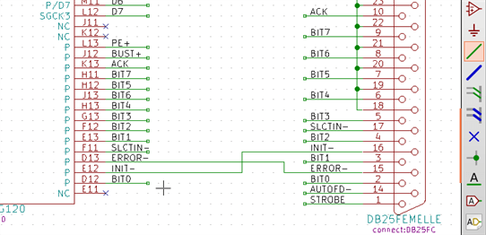
Note 3 :
Les fils qui se croisent ne sont pas implicitement connectés. Il est nécessaire de les joindre avec un point de jonction si une connexion est souhaitée.
La figure précédente montre un cas de connexions utilisant des symboles de jonction (fils reliés entre eux, DB25FEMALE pins 19, 20, 21, 22).
Note 4 :
Si deux labels différents sont placés sur le même fil, ils sont reliés entre eux et deviennent équivalents. Et tous les éléments reliés à l’un ou l’autre de ces labels seront connectés entre eux.
Connexions (Bus)
Dans le schéma ci-dessous, de nombreuses pins sont connectées à des bus.
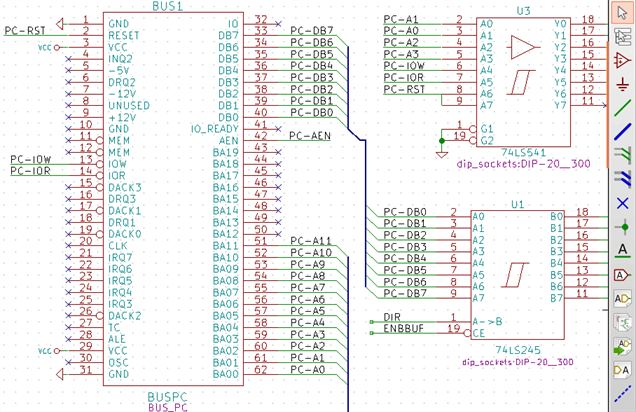
Membres d’un bus
Du point de vue schématique, un bus est une collection de signaux, commençant par un préfixe commun, et se terminant par un numéro. Par exemple, PCA0, PCA1, PCA2 et sont des membres du bus PCA.
Le bus complet est nommé PCA[N..m], où N et m sont le premier et le dernier numéro des fils de ce bus. Ainsi, si le bus PCA compte 20 membres, de 0 à 19, le bus complet sera noté PCA[0..19]. Une collection de signaux comme PCA0, PCA1, PCA2, WRITE, READ ne peut être contenue dans un bus.
Connexions entre membres de bus
Les pins connectées entre les membres d’un même bus doivent être reliées par des labels. Il est impossible de connecter une pin directement à un bus ; ce type de connexion sera ignoré par Eeschema.
Dans l’exemple ci-dessus, les connexions sont faites par des labels placés sur les fils connectés aux pins. Les entrées de bus (segments de fil à 45 degrés) sont purement décoratifs, et ne sont pas nécessaires pour établir des connexions logiques.
En pratique, en utilisant la commande de répétition (touche Insert), les connexions peuvent être très vite faites de la façon suivante, si les pins de composants sont alignées dans l’ordre croissant (un cas fréquent sur des composants tels que des mémoires, microprocesseurs, etc…) :
-
Placez le premier label (par exemple PCA0).
-
Utilisez la commande de répétition autant de fois que nécessaire pour placer les autres membres. Eeschema créera automatiquement les labels suivants (PCA1, PCA2 …) alignés verticalement, théoriquement sur la position des autres pins.
-
Dessinez le fil sous le premier label. Ensuite, utilisez la commande de répétition pour placer les autres fils sous les autres labels.
-
Au besoin, placez les entrées de bus de la même façon (placez la première entrée, puis utilisez la commande de répétition).
|
Dans le menu Préférences / Options de l’éditeur de schématique, vous pouvez définir les paramètres de répétition :
|
Connexions globales entre les bus
Vous pouvez avoir besoin de mettre des connexions entre des bus, pour, par exemple, relier deux bus ayant des noms différents, ou dans le cas d’une hiérarchie, pour créer des liens entre les différentes feuilles. Dans ce cas, effectuez ces connexions de la manière suivante :
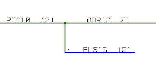
Les bus PCA [0..15], ADR [0..7] et BUS [5..10] sont reliés entre eux (remarquez la jonction placée ici pour que le fil de bus vertical rejoigne le milieu du segment du bus horizontal).
Plus précisément, les éléments correspondants sont reliés entre eux: PCA0, ADR0 sont connectés, (de même que PCA1 et ADR1, …, PCA7 et ADR7).
De la même manière, PCA5, BUS5 et ADR5 sont connectés (tout comme PCA6, BUS6 et ADR6 et PCA7, BUS7 et ADR7).
PCA8 et BUS8 sont aussi connectés (tout comme PCA9 et BUS9, PCA10 et BUS10)
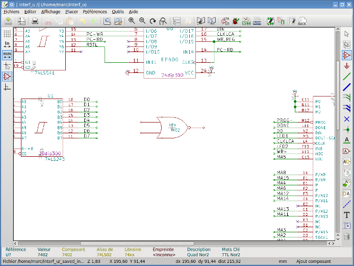
Connexion des sources d’alimentation
When the power pins of the symbols are visible, they must be connected, as for any other signal.
Symbols such as gates and flip-flops may have invisible power pins. Care must be taken with these because:
-
Vous ne pouvez pas connecter de fils, en raison de leur invisibilité.
-
Vous ne connaissez pas leurs noms.
Et de plus, ce serait une mauvaise idée de les rendre visibles et de les relier comme les autres pins, parce que le schéma deviendrait illisible et non conforme aux conventions habituelles.
|
Si vous voulez forcer l’affichage de ces pins d’alimentation invisibles, vous devez cocher l’option «Afficher les pins invisibles» dans la boîte de dialogue du menu Préférences / Options de l’éditeur de schématique, ou cliquer sur l’icône |
Eeschema connecte automatiquement les pins d’alimentation invisibles de même nom, à la source d’alimentation portant ce nom. Il peut être nécessaire de relier des points d’alimentation de noms différents (par exemple, "GND" dans les composants TTL et "VSS" dans les composants MOS) ; utilisez les symboles d’alimentation pour cela.
Il est déconseillé d’utiliser des labels pour le raccordement aux alimentations. Ceux-ci ne disposent que d’une portée de connexion "locale", et ne relieraient pas les pins d’alimentation invisibles.
La figure ci-dessous montre un exemple de connexion de sources d’alimentation.
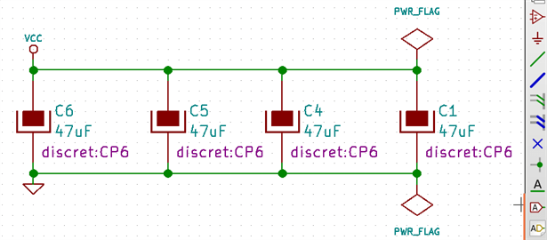
Dans cet exemple, la masse (GND) est connectée à la source d’alimentation VSS, et la source d’alimentation VCC est connectée à VDD.
Deux symboles PWR_FLAG y sont visibles. Ils indiquent que les deux sources d’alimentation VCC et GND sont vraiment reliées à une source d’alimentation. Sans ces deux drapeaux, l’outil ERC diagnostiquerait : Warning Avertissement : port d’alimentation non connecté.
All these symbols can be found in the ``power'' symbol library.
``No Connect'' flag
These symbols are very useful to avoid undesired ERC warnings. The electrical rules check ensures that no connection has been accidentally left unconnected.
Si des pins doivent vraiment rester en l’air, il est nécessaire de placer un drapeau, symbole de "Non Connexion" (outil : ![]() ) sur ces broches. Ces symboles n’ont aucune incidence sur la génération des netlistes.
) sur ces broches. Ces symboles n’ont aucune incidence sur la génération des netlistes.
Compléments Graphiques
Textes et Commentaires
It can be useful (to aid in understanding the schematic) to place annotations such as text fields and frames. Text fields (tool ![]() ) and Polyline (tool
) and Polyline (tool ![]() ) are intended for this use, contrary to labels and wires, which are connection elements.
) are intended for this use, contrary to labels and wires, which are connection elements.
Ici, un exemple de cadre avec un texte de commentaire :
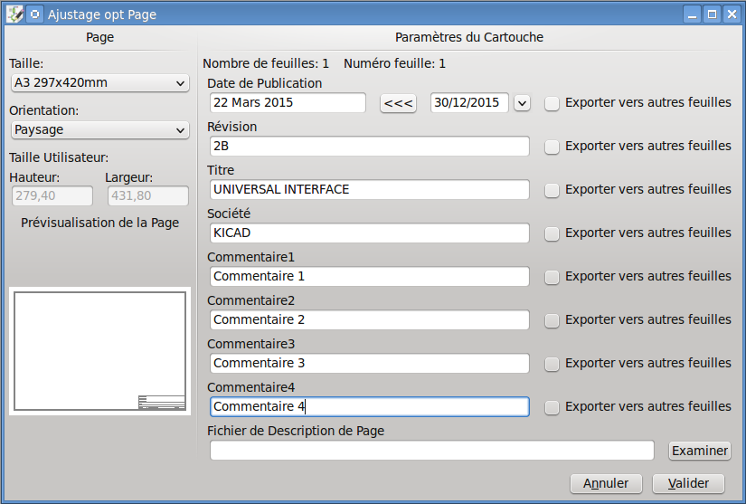
Cartouche
On peut modifier le cartouche et son contenu en cliquant sur l’outil ![]() .
.
Le nombre et le numéro de feuille sont automatiquement mis à jour.
Rescuing cached symbols
By default, Eeschema loads symbols from the project libraries according to the set paths and library order. This can cause a problem when loading a very old project: if the symbols in the library have changed or have been removed or the library no longer exists since they were used in the project, the ones in the project would be automatically replaced with the new versions. The new versions might not line up correctly or might be oriented differently leading to a broken schematic.
When a project is saved, a cache library with the contents of the current library symbols is saved along with the schematic. This allows the project to be distributed without the full libraries. If you load a project where symbols are present both in its cache and in the system libraries, Eeschema will scan the libraries for conflicts. Any conflicts found will be listed in the following dialog:
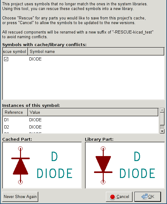
You can see in this example that the project originally used a diode with the cathode facing up, but the library now contains one with the cathode facing down. This change would break the schematic! Pressing OK here will cause the symbol cache library to be saved into a special ``rescue'' library and all the symbols are renamed to avoid naming conflicts.
If you press Cancel, no rescues will be made, so Eeschema will load all the new components by default. If you save the schematic at this point, your cache will be overwritten and the old symbols will not be recoverable. If you have saved the schematic, you can still go back and run the rescue function again by selecting "Rescue Cached Components" in the "Tools" menu to call up the rescue dialog again.
If you would prefer not to see this dialog, you can press "Never Show Again". The default will be to do nothing and allow the new components to be loaded. This option can be changed back in the Libraries preferences.
Schématiques hiérarchiques
Introduction
Une représentation hiérarchique est généralement une bonne solution pour des projets dépassant quelques feuilles. Si vous voulez gérer ce type de projet, il vous faudra :
-
Utiliser de grande feuilles, ce qui pourrait conduire à des problèmes d’impression ou de manipulation.
-
Utiliser plusieurs feuilles, ce qui vous amène à une structure hiérarchique.
La schématique complète consiste alors en une feuille principale, appelée feuille racine, et des sous-feuilles constituant la hiérarchie. En outre, une habile subdivision du schéma en plusieurs feuilles augmentera souvent sa lisibilité.
À partir de la feuille racine, vous pouvez accéder à toutes les sous-feuilles. La gestion d’une schématique hiérarchique est très facile avec Eeschema, grâce à son "Navigateur de Hiérarchie" accessible par l’icône ![]() de la barre d’outils supérieure.
de la barre d’outils supérieure.
There are two types of hierarchy that can exist simultaneously: the first one has just been evoked and is of general use. The second consists in creating symbols in the library that appear like traditional symbols in the schematic, but which actually correspond to a schematic which describes their internal structure.
Le second type est utilisé pour concevoir des circuits intégrés, car dans ce cas vous devez utiliser des librairies de fonctions dans le schéma que vous êtes en train de dessiner.
Eeschema ne gère pas pour l’instant ce deuxième type.
Une hiérarchie peut être :
-
simple : une feuille donnée n’est utilisée qu’une seule fois.
-
complexe : une feuille donnée sera utilisée plusieurs fois (instances multiples).
-
à plat : c’est un hiérarchie simple, mais les liaisons entre feuilles ne sont pas dessinées.
Eeschema est capable de gérer ces différentes hiérarchies.
La création d’une schématique hiérarchique est facile, la hiérarchie étant manipulée à partir de la feuille racine, comme si vous n’aviez qu’un seul schéma.
Les deux étapes importantes à comprendre sont :
-
Comment créer une sous-feuille.
-
How to build electrical connections between sub-sheets.
Navigation dans la hiérarchie
Navigation among sub-sheets is acheived by using the navigator tool accessible via the button ![]() on the top toolbar.
on the top toolbar.
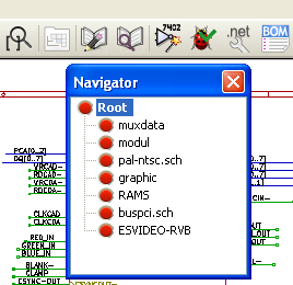
Each sheet is reachable by clicking on its name. For quick access, right click on a sheet name, and choose to Enter Sheet or double click within the bounds of the sheet.
In order to exit the current sheet to the parent sheet, right click anywhere in the schematic where there is no object and select "Leave Sheet" in the context menu or press Alt+Backspace.
Labels locaux, hiérarchiques et globaux
Propriétés
Les labels locaux, outil ![]() , relient des signaux uniquement à l’intérieur de la même feuille. Les labels hiérarchiques, outil
, relient des signaux uniquement à l’intérieur de la même feuille. Les labels hiérarchiques, outil ![]() , relient des signaux uniquement à l’intérieur d’une feuille ou à une pin hiérarchique de sa feuille parente.
, relient des signaux uniquement à l’intérieur d’une feuille ou à une pin hiérarchique de sa feuille parente.
Les labels globaux, outil ![]() , relient des signaux à travers toute la hiérarchie. Les pins d’alimentation (de type power in et power out) invisibles sont similaires aux labels globaux car elles sont reliées à travers toute la hiérarchie.
, relient des signaux à travers toute la hiérarchie. Les pins d’alimentation (de type power in et power out) invisibles sont similaires aux labels globaux car elles sont reliées à travers toute la hiérarchie.
| À l’intérieur d’une hiérarchie, on peut utiliser à la fois des labels globaux ou hiérarchiques. |
Summary of hierarchy creation
Vous devez :
-
Placer dans la feuille racine un symbole appelé "Feuille hiérarchique".
-
Accéder à cette nouvelle feuille schématique (sous-feuille) par le navigateur, et la dessiner, comme n’importe quel schéma.
-
Draw the electric connections between the two schematics by placing Global Labels (HLabels) in the new schematic (sub-sheet), and labels having the same name in the root sheet, known as SheetLabels. These SheetLabels will be connected to the sheet symbol of the root sheet to the other elements of the schematic like standard symbol pins.
Symbole de feuille hiérarchique
Tracez un rectangle symbolisant la sous-feuille, en plaçant deux points sur une diagonale.
La taille de ce rectangle vous permettra d’ajouter plus tard des labels particuliers, des pins de hiérarchie, correspondant aux labels globaux (Hlabels) de la sous-feuille.
These labels are similar to usual symbol pins. Select the tool ![]() .
.
Cliquez pour placer le coin supérieur gauche du rectangle. Cliquez à nouveau pour positionner le coin inférieur droit, afin d’avoir un rectangle suffisamment grand.
On vous demandera alors de donner un nom de fichier et un nom de feuille pour cette sous-feuille, pour vous permettre de l’atteindre par le navigateur de hiérarchie.
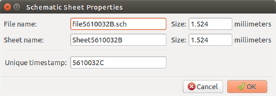
Vous devez au moins spécifier un nom de fichier. En l’absence de nom de feuille, c’est le nom de fichier qui sera utilisé comme nom de feuille (c’est la méthode habituelle).
Connexions - Pins hiérarchiques
Vous allez maintenant créer des points de connexion (pins hiérarchiques) pour le symbole de feuille qui vient d’être créé.
These points of connection are similar to normal symbol pins, with however the possibility to connect a complete bus with only one point of connection.
Il y a deux méthodes possibles :
-
Placer les différentes pins avant le dessin de la sous-feuille (placement manuel).
-
Placer les différentes pins après le dessin de la sous-feuille et des labels globaux (placement semi-automatique).
Cette deuxième méthode largement préférable.
Placement manuel
-
Select the tool
 .
. -
Click on the hierarchy symbol where you want to place the pin.
See below for an example of creating a hierarchical pin named "CONNECTION":
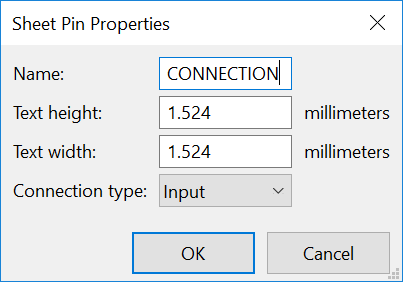
You can define the name, size and direction of the pin during creation or later, by right clicking the pin and selecting Edit Sheet Pin in the popup menu.
Inside the sheet a Hierarchical Label must be preset with the same name as the Hierarchical Pin. Taking care to correctly match these names must be done manually, which is why the second method, below, is preferred.
Placement automatique :
-
Sélectionnez l’outil
 .
. -
Cliquez sur le symbole de feuille hiérarchique dans lequel vous voulez importer des pins hiérarchiques correspondant aux labels hiérarchiques placés dans la feuille correspondante. Une pin hiérarchique apparaît si un label hiérarchique existe et qu’il ne correspond pas à une pin déjà placée.
-
Cliquez où vous souhaiter placer la pin.
Les pins nécessaires peuvent ainsi être placées rapidement et sans erreur. Leur aspect correspond à celui de leur label hiérarchique.
Connexions - Labels hiérarchiques
À chaque pin de la feuille symbolique venant d’être créée doit correspondre un label appelé label hiérarchique dans la sous-feuille. Les labels hiérarchiques sont similaires aux labels ordinaires, mais ils permettent des connexions entre les sous-feuilles et la feuille de racine. La représentation graphique de ces deux éléments complémentaires (pin et label hiérarchiques) est identique. La création de labels hiérarchiques se fait à l’aide de l’outil : ![]() .
.
Ci-dessous un exemple de feuille racine :
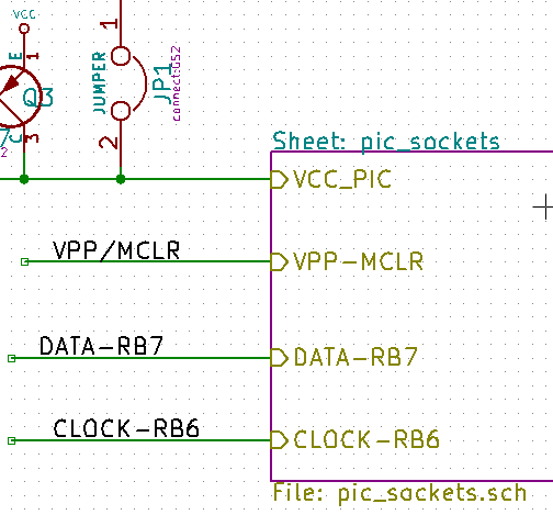
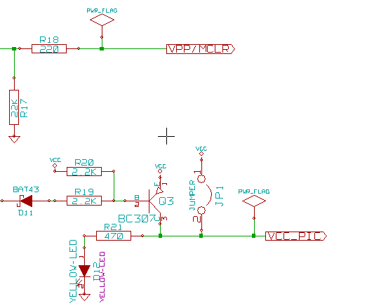
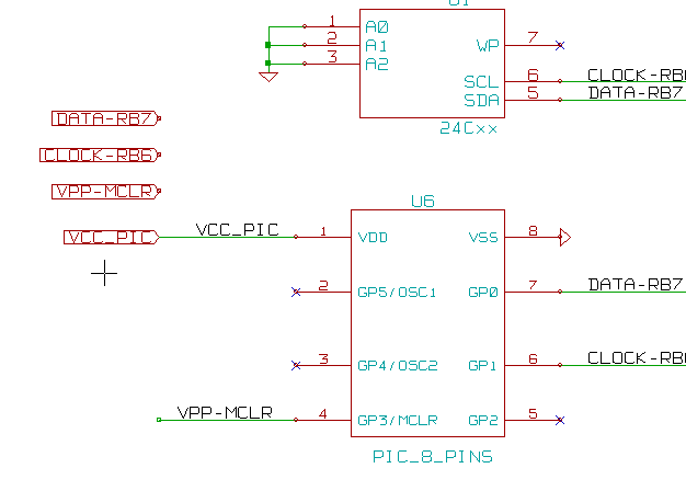
Remarquez la pin hiérarchique VCC-PIC, reliée au connecteur JP1.
Voici les connexions correspondantes dans la sous-feuille :
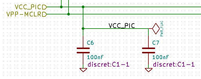
Nous retrouvons les deux labels hiérarchiques correspondants, qui établissent la connexion entre les deux feuilles hiérarchiques.
| Vous pouvez utiliser des pins et des labels hiérarchiques pour relier deux bus, en utilisant la syntaxe décrite précédemment (Bus [N..m]). |
Labels, labels hiérarchiques, labels globaux et pins d’alimentation invisibles
Quelques remarques sur les différentes façons d’établir des connexions autrement qu’avec des fils.
Labels simples
Les labels simples n’ont qu’une portée locale de connexion, limitée à la feuille de schéma dans laquelle ils sont placés. Ceci est du au fait que :
-
Chaque feuille a un numéro de feuille.
-
Ce numéro de feuille est associé à l’étiquette.
Ainsi, quand vous placez un label "TOTO" dans la feuille n°3, le vrai nom de ce label est "TOTO_3". Si vous avez aussi un label "TOTO" dans la feuille n°1 (feuille racine), c’est en fait un label "TOTO_1" différent de "TOTO_3". Ceci est toujours vrai, même si vous n’avez qu’une seule feuille.
Labels hiérarchiques
Ce que nous avons dit pour les labels simple est vrai aussi pour les labels hiérarchiques.
Thus in the same sheet, a hierarchical label "TOTO" is considered to be connected to a local label "TOTO", but not connected to a hierarchical label or label called "TOTO" in another sheet.
A hierarchical label is considered to be connected to the corresponding sheet pin symbol in the hierarchical symbol placed in the parent sheet.
Pins d’alimentations invisibles
It was seen that invisible power pins were connected together if they have the same name. Thus all the power pins declared "Invisible Power Pins" and named VCC are connected all symbol invisible power pins named VCC only within the sheet they are placed.
En revanche, si vous placez un label VCC dans une sous-feuille, il ne sera pas relié aux pins VCC, parce que ce label est en fait VCC_n, où n est le numéro de la feuille.
If you want this label VCC to be really connected to the VCC for the entire schematic, it will have to be explicitly connected to an invisible power pin via a VCC power symbol.
Labels globaux
Les labels globaux qui portent le même nom sont connectés à travers toute la hiérarchie.
(les labels d’alimentation comme vcc … sont des labels globaux)
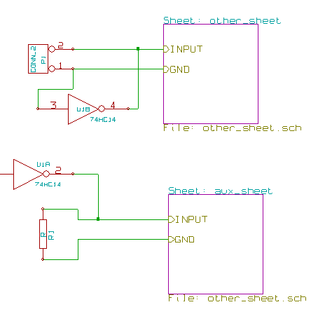
Hiérarchie complexe
Here is an example. The same schematic is used twice (two instances). The two sheets share the same schematic because the file name is the same for the two sheets (``other_sheet.sch''). The sheet names must be unique.
Hiérarchie à plat
You can create a project using many sheets without creating connections between these sheets (flat hierarchy) if the following rules are observed:
-
Create a root sheet containing the other sheets which acts as a link between others sheets.
-
Aucune connexion explicite n’est nécessaire.
-
Use global labels instead of hierarchical labels in all sheets.
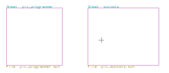
Voici un exemple de feuille racine :
Voici les deux feuilles, connectées par des labels globaux.
Voici la feuille pic_programmer.sch.
Voici la feuille pic_sockets.sch.
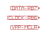
Regardez les labels globaux.
Symbol Annotation Tool
Introduction
The annotation tool allows you to automatically assign a designator to symbols in your schematic. Annotation of symbols with multiple units will assign a unique suffix to minimize the number of these symbols. The annotation tool is accessible via the icon ![]() . Here you find its main window.
. Here you find its main window.
Available annotation schemes:
-
Annotate all the symbols (reset existing annotation option)
-
Annotate all the symbols, but do not swap any previously annotated multi-unit parts.
-
Annotate only symbols that are currently not annotated. Symbols that are not annotated will have a designator which ends with a '?' character.
-
Annoter toute la hiérarchie (Utiliser la schématique entière).
-
Annoter seulement le schéma en cours (Utiliser la feuille active uniquement).
The ``Reset, but do not swap any annotated multi-unit parts'' option keeps all existing associations between symbols with multilple units. For example, U2A and U2B may be reannotated to U1A and U1B respectively but they will never be reannotated to U1A and U2A, nor to U2B and U2A. This is useful if you want to ensure that pin groupings are maintained.
Le choix de l’ordre de l’annotation fixe la méthode utilisée pour affecter les numéros de référence sur chaque feuille de la hiérarchie.
Sauf exception, l’annotation automatique s’applique au projet entier (toutes les feuilles) et aux nouveaux composants, si on ne veut pas modifier les annotations précédentes.
The Annotation Choice gives the method used to calculate reference:
-
Use first free number in schematic: components are annotated from 1 (for each reference prefix). If a previous annotation exists, only unused numbers will be used.
-
Démarrer à numéro de feuille *100 et utiliser le premier nombre libre : l’annotation commence par 101 sur la feuille numéro 1, par 201 sur la feuille numéro 2, etc… S’il y a plus de 99 éléments avec le même préfixe de référence (U, R) sur la feuille 1, l’outil d’annotation utilisera le numéro 200 et suivants, et l’annotation de la feuille 2 commencera au prochain numéro libre.
-
Démarrer à numéro de feuille *1000 et utiliser le premier nombre libre : l’annotation commence par 1001 sur la feuille numéro 1, par 2001 sur la feuille numéro 2, etc…
Quelques exemples
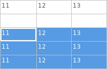
Ordre d’annotation
Cet exemple montre 5 composants, non encore annotés.
Après l’exécution de l’annotation automatique, on obtient le résultat suivant.
Composants triés par position X.
Composants triés par position Y.
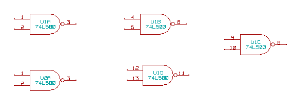
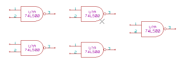
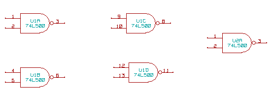
Vous pouvez voir que quatre portes 74LS00 ont été réparties dans le boitier U1, et que la cinquième porte 74LS00 a été assignée au suivant, U2.
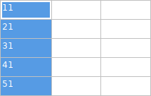
Choix de l’annotation
Voici une annotation de la feuille 2 avec l’option 'Utiliser le premier nombre libre de la schématique'.
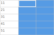
L’option 'Démarrer à numéro de feuille *100 et utiliser le premier nombre libre' donne le résultat suivant.
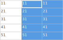
L’option 'Démarrer à numéro de feuille *1000 et utiliser le premier nombre libre' donne le résultat suivant.
Vérification des règles électriques (ERC)
Introduction
L’outil de vérification des règles électriques, ou ERC (Electrical Rules Check), vérifie automatiquement votre schéma. Il détecte les erreurs dans la feuille, comme les pins ou les symboles hiérarchiques non connectés, les sorties en court-circuit, etc… Bien entendu une vérification automatique n’est pas infaillible, et le logiciel qui la réalise n’est pas encore terminé à 100%. Malgré tout, cette vérification est très utile, car elle détecte beaucoup d’omissions et de petites erreurs.
In fact all detected errors must be checked and then corrected before proceeding as normal. The quality of the ERC is directly related to the care taken in declaring electrical pin properties during symbol library creation. ERC output is reported as errors'' or warnings''.
Utilisation de l’ERC
L’ERC est lancé par l’icône ![]() .
.
Des avertissements, sous forme de petites flèches de marquage, seront placés sur les éléments schématiques générant une erreur ERC (pins ou labels).
|
Vous pouvez également supprimer des marqueurs d’erreur dans la boîte de dialogue.
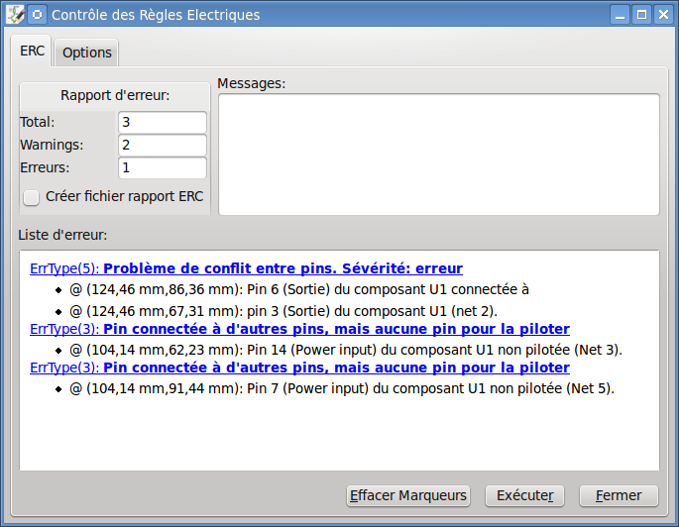
Exemple d’ERC
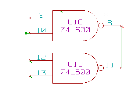
Ici, vous pouvez voir quatre erreurs :
-
Deux sorties logiques ont été reliées ensemble (flèche rouge).
-
Deux entrées ne sont pas connectées (flèches vertes du bas).
-
Une erreur sur une source d’alimentation invisible, dont il manque le symbole d’alimentation (flèche verte du haut).
Affichage du diagnostic
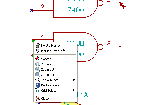
Un clic droit sur un marqueur vous affiche le menu contextuel permettant d’accéder à la fenêtre d’informations de diagnostic de l’ERC.
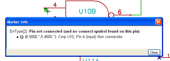
et en cliquant sur un marqueur, vous obtenez une description de l’erreur.
Pins d’alimentation et symboles d’alimentation (Power Flag)
Il est fréquent d’avoir une erreur ou un avertissement sur les pins d’alimentation, même si tout semble normal. Voir l’exemple ci-dessus. Cela arrive parce que, dans la plupart des dessins, l’alimentation est fournie par des connecteurs qui ne sont pas identifiés comme des sources d’énergie (au contraire d’une sortie de régulateur qui, elle, est déclarée en tant que sortie d’alimentation).
Ainsi l’ERC ne détectera pas une pin de sortie d’alimentation pour ce fil et le déclarera non-connecté à une source d’alimentation.
Pour éviter ceci, il faut placer un symbole d’alimentation, "PWR_FLAG", sur ce connecteur d’alim. Comme dans l’exemple suivant :
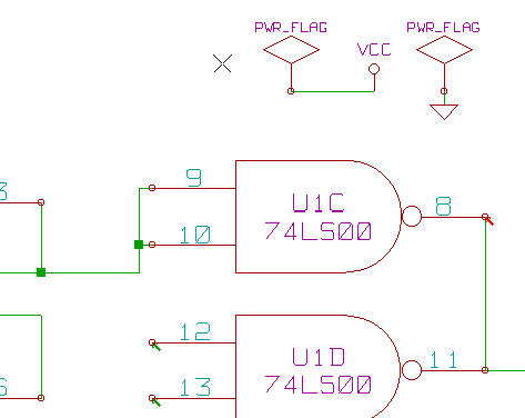
Et ainsi le marqueur disparaît.
Most of the time, a PWR_FLAG must be connected to GND, because regulators have outputs declared as power out, but ground pins are never power out (the normal attribute is power in), so grounds never appear connected to a power source without a power flag symbol.
Configuration
Le panneau des Options vous permet de configurer les règles de connexion définissant les conditions électriques de la vérification des erreurs et des avertissements.
Les règles sont modifiées en cliquant plusieurs fois sur le bouton carré dans le tableau pour faire défiler les différents choix : normal [vert], avertissement [W jaune], erreur [E rouge].
Fichier de rapport d’ERC
An ERC report file can be generated and saved by checking the option Write ERC report. The file extension for ERC report files is .erc. Here is an example ERC report file.
ERC control (4/1/1997-14:16:4)

***** Sheet 1 (INTERFACE UNIVERSAL)
ERC: Warning Pin input Unconnected @ 8.450, 2.350
ERC: Warning passive Pin Unconnected @ 8.450, 1.950
ERC: Warning: BiDir Pin connected to power Pin (Net 6) @ 10.100, 3.300
ERC: Warning: Power Pin connected to BiDir Pin (Net 6) @ 4.950, 1.400

>> Errors ERC: 4
Création d’une Netliste
Généralités
A netlist is a file which describes electrical connections between symbols. These connections are referred to as nets. In the netlist file you can find:
-
The list of the symbols
-
The list of connections (nets) between symbols.
Many different netlist formats exist. Sometimes the symbols list and the list of nets are two separate files. This netlist is fundamental in the use of schematic capture software, because the netlist is the link with other electronic CAD software such as:
-
PCB layout software.
-
Schematic and electrical signal simulators.
-
les compilateurs de CPLD (et autres circuits intégrés programmables).
Eeschema gère plusieurs formats de netlistes.
-
Le format PCBNEW (circuits imprimés).
-
Le format ORCAD PCB2 (circuits imprimés).
-
Le format CADSTAR (circuits imprimés).
-
Le format SPICE, utilisé par différents simulateurs.
Formats de Netliste
Select the tool ![]() to open the netlist creation dialog.
to open the netlist creation dialog.
Onglet Pcbnew :
Onglet Spice :
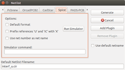
Using the different tabs you can select the desired format. In Spice format you can generate netlists with either net names which makes the SPICE file more human readable or net numbers which are used by older Spice. By clicking the Netlist button, you will be asked for a netlist file name.
| The netlist generation can take up to several minutes for large schematics. |
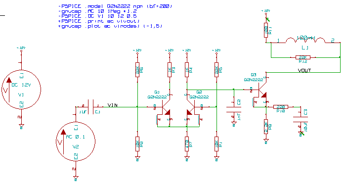
Exemples de netlistes
Vous pouvez voir ci-dessous un schéma
Exemple d’une netliste pour PcbNew :
# Eeschema Netlist Version 1.0 generee le 21/1/1997-16:51:15
(
(32E35B76 $noname C2 1NF {Lib=C}
(1 0)
(2 VOUT_1)
)
(32CFC454 $noname V2 AC_0.1 {Lib=VSOURCE}
(1 N-000003)
(2 0)
)
(32CFC413 $noname C1 1UF {Lib=C}
(1 INPUT_1)
(2 N-000003)
)
(32CFC337 $noname V1 DC_12V {Lib=VSOURCE}
(1 +12V)
(2 0)
)
(32CFC293 $noname R2 10K {Lib=R}
(1 INPUT_1)
(2 0)
)
(32CFC288 $noname R6 22K {Lib=R}
(1 +12V)
(2 INPUT_1)
)
(32CFC27F $noname R5 22K {Lib=R}
(1 +12V)
(2 N-000008)
)
(32CFC277 $noname R1 10K {Lib=R}
(1 N-000008)
(2 0)
)
(32CFC25A $noname R7 470 {Lib=R}
(1 EMET_1)
(2 0)
)
(32CFC254 $noname R4 1K {Lib=R}
(1 +12V)
(2 VOUT_1)
)
(32CFC24C $noname R3 1K {Lib=R}
(1 +12V)
(2 N-000006)
)
(32CFC230 $noname Q2 Q2N2222 {Lib=NPN}
(1 VOUT_1)
(2 N-000008)
(3 EMET_1)
)
(32CFC227 $noname Q1 Q2N2222 {Lib=NPN}
(1 N-000006)
(2 INPUT_1)
(3 EMET_1)
)
)
# End
La même netliste, en format PSPICE :
* Eeschema Netlist Version 1.1 (Spice format) creation date: 18/6/2008-08:38:03

.model Q2N2222 npn (bf=200)
.AC 10 1Meg \*1.2
.DC V1 10 12 0.5


R12   /VOUT N-000003 22K
R11   +12V N-000003 100
L1   N-000003 /VOUT 100mH
R10   N-000005 N-000004 220
C3   N-000005 0 10uF
C2   N-000009 0 1nF
R8   N-000004 0 2.2K
Q3   /VOUT N-000009 N-000004 N-000004 Q2N2222
V2   N-000008 0 AC 0.1
C1   /VIN N-000008 1UF
V1   +12V 0 DC 12V
R2   /VIN 0 10K
R6   +12V /VIN 22K
R5   +12V N-000012 22K
R1   N-000012 0 10K
R7   N-000007 0 470
R4   +12V N-000009 1K
R3   +12V N-000010 1K
Q2   N-000009 N-000012 N-000007 N-000007 Q2N2222
Q1   N-000010 /VIN N-000007 N-000007 Q2N2222

.print ac v(vout)
.plot ac v(nodes) (-1,5)

.end
Notes sur les netlistes
Précautions pour les noms de netlistes
Many software tools that use netlists do not accept spaces in the component names, pins, nets or other informations. Avoid using spaces in labels, or names and value fields of components or their pins to ensure maximum compatibility.
De la même manière, les caractères spéciaux autres que les lettres et les chiffres peuvent poser problème. Notez que cette limitation n’est pas propre à Eeschema, mais aux formats de netlistes qui pourraient s’avérer intraduisibles pour les logiciels qui les utilisent.
Netlistes PSPICE
Pour le simulateur PSPICE, vous devez inclure certaines commandes dans la netliste elle-même (.PROBE, .AC, etc..).
Chaque ligne de texte incluse dans le schéma et débutant par les mots-clefs -pspice ou -gnucap sera insérée (sans le mot-clef) au début de la netliste.
Chaque ligne de texte incluse dans le schéma et débutant par les mots-clefs +pspice ou +gnucap sera insérée (sans le mot-clef) à la fin de la netliste.
Voici un exemple utilisant plusieurs lignes de texte et un autre utilisant un texte multi-lignes :
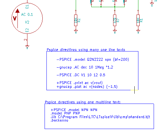
Par exemple, si vous tapez le texte suivant (n’utilisez pas un label !) :
-PSPICE .PROBE
une ligne .PROBE sera insérée en début de netliste.
Dans l’exemple précédent, avec cette méthode, trois lignes étaient insérées au début de la netliste et deux à la fin.
Si vous utilisez un texte multi-lignes, les mots-clefs +pspice ou +gnucap ne sont nécessaires qu’une seule fois :
+PSPICE .model NPN NPN
.model PNP PNP
.lib C:\Program Files\LTC\LTspiceIV\lib\cmp\standard.bjt
.backanno
crée les quatre lignes :
.model NPN NPN
.model PNP PNP
.lib C:\Program Files\LTC\LTspiceIV\lib\cmp\standard.bjt
.backanno
Also note that the GND net must be named 0 (zero) for Pspice.
Autres formats
Pour d’autres formats de netlistes, vous pouvez ajouter des convertisseurs de netlistes sous forme de plugins. Ces convertisseurs seront lancés automatiquement par Eeshema. Le chapitre 14 donne des explications et quelques exemples de convertisseurs.
Un convertisseur est un fichier texte (format XSL), mais on peut utiliser d’autres langages, comme Python. Lorsque vous utilisez le format XSL, un outil (xsltproc.exe ou xsltproc) lit le fichier intermédiaire créé par Eeschema et le fichier de conversion pour créer le fichier de sortie. Dans ce cas, le fichier de conversion (une feuille de style) est très petit et très facile à écrire.
Ajout dans la boite de dialogue
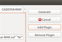
Vous pouvez ajouter un nouveau plugin par le bouton "Ajouter Plugin".
Voici la fenêtre de configuration pour un plugin PadsPcb :
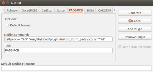
La configuration demande :
-
Un titre pour l’onglet (comme le nom du format de Netliste).
-
La ligne de commande du plugin à lancer.
Quand la liste est créée :
-
Eeschema crée un fichier temporaire intermédiaire .tmp, par exemple test.tmp.
-
Eeschema lance le plugin, qui lit ce test.tmp et crée la netliste test.net.
Format de la ligne de commande
Voici un exemple de ligne de commande utilisant xsltproc.exe comme outil de conversion de fichiers .xsl et un fichier netlist_form_pads-pcb.xsl qui sert de feuille de style :
f:/kicad/bin/xsltproc.exe -o %O.net f:/kicad/bin/plugins/netlist_form_pads-pcb.xsl %I
avec :
| f:/kicad/bin/xsltproc.exe | A tool to read and convert xsl file |
|---|---|
-o %O.net |
Output file: %O will define the output file. |
f:/kicad/bin/plugins/netlist_form_pads-pcb.xsl |
File name converter (a sheet style, xsl format). |
%I |
Will be replaced by the intermediate file created by Eeschema (*.tmp). |
Pour un schéma nommé test.sch, la ligne de commande réelle qui en résulterait :
f:/kicad/bin/xsltproc.exe -o test.net f:/kicad/bin/plugins/netlist_form_pads-pcb.xsl test.tmp.
Convertisseur et feuille de style
C’est un logiciel très simple, parce que son rôle est seulement de convertir un fichier texte d’entrée (le fichier intermédiaire) en un autre fichier texte. À partir du fichier intermédiaire, vous pouvez, en outre, créer une liste des composants (BOM).
Lors de l’utilisation de xsltproc comme convertisseur, seul le contenu décrit dans la feuille de style sera généré.
Format du fichier intermédiaire de Netliste
Voir le chapitre 14 pour plus d’explications au sujet de xsltproc, du fichier intermédiaire, et des exemples de feuilles de style pour le convertisseur.
Tracer / Imprimer
Introduction
Les commandes 'Imprimer' et 'Tracer' sont accessibles par le menu 'Fichiers'.
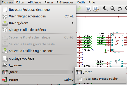
Les formats de sortie peuvent être : Postscript, PDF, SVG, DXF ou HPGL. Vous pouvez aussi imprimer directement sur votre imprimante.
Commandes de tracé communes
- Tracer Page Courante
-
génère un fichier pour la feuille courante seulement.
- Tracer Toutes les Pages
-
vous permet de tracer toute la hiérarchie (un fichier est généré pour chaque feuille).
Tracer en Postscript
Cette commande vous permet de générer des fichiers au format PostScript.
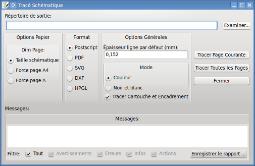
Le nom du fichier généré est le nom de la feuille avec l’extension .ps. Vous pouvez désactiver l’option "Tracer cartouche et encadrement". Ceci est utile quand vous voulez créer un fichier PostScript pour l’encapsulation (format .eps), utilisé pour insérer une figure dans un logiciel de traitement de texte. La fenêtre de message affiche le chemin et le nom des fichiers créés.
Tracer en PDF
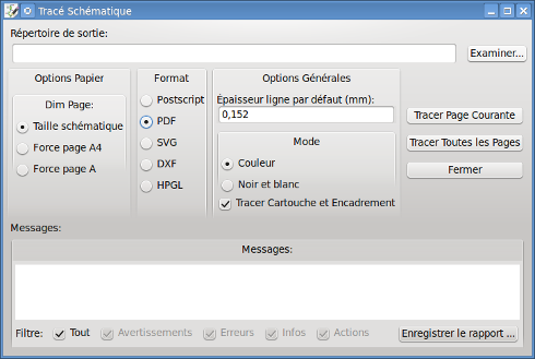
Vous permet de générer un tracé au format PDF. Le nom du fichier généré est le nom de la feuille avec l’extension .pdf.
Tracer en SVG
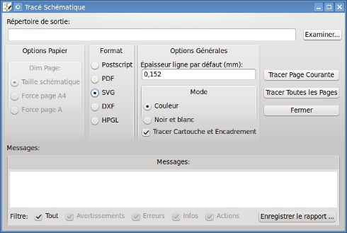
Vous permet de générer un tracé au format vectoriel SVG. Le nom du fichier généré est le nom de la feuille avec l’extension .svg.
Tracer en DXF
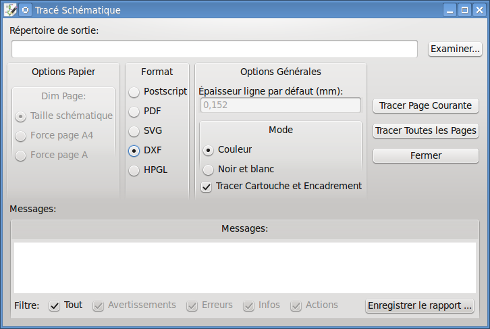
Vous permet de générer un tracé au format DXF. Le nom du fichier généré est le nom de la feuille avec l’extension .dxf.
Tracer en HPGL
Vous permet de générer un tracé au format HPGL. Pour ce format, vous pouvez définir :
-
La taille de page.
-
L’origine.
-
La taille du pinceau (en mm).
La fenêtre de configuration du tracé ressemble à ceci :
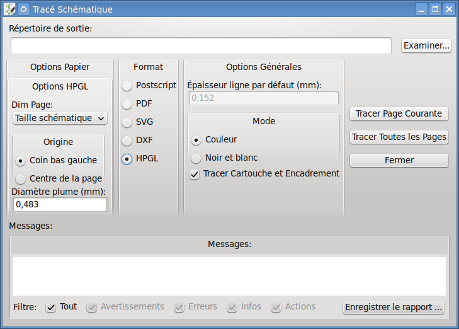
Le nom du fichier généré sera le nom de la feuille avec l’extension .plt.
Sélection de la taille de la feuille schématique
La case 'Taille Shématique' est normalement cochée. Dans ce cas, la taille de la feuille définie dans les options de la page sera utilisée, et l’échelle choisie sera de 1. Si une autre taille de feuille est sélectionnée (de A4 à A0, de A à E, etc..), l’échelle sera automatiquement ajustée pour remplir la page.
Ajustement des décalages
Pour toutes les dimensions standards, vous pouvez ajuster les décalages pour centrer le dessin aussi précisément que possible. Certains traceurs ayant un point d’origine au centre, et d’autres au coin inférieur droit, il est nécessaire de pouvoir introduire un décalage pour tracer correctement.
Généralement :
-
Pour des traceurs ayant leur point d’origine au centre de la feuille, le décalage doit être négatif et fixé à la moitié de la dimension de la feuille.
-
Pour des traceurs ayant leur point d’origine dans le coin inférieur gauche de la feuille, le décalage doit être réglé à 0.
Pour fixer un décalage :
-
Sélectionnez la taille de la feuille.
-
Fixez les décalages X et Y.
-
Cliquez sur accepter les décalages.
Imprimer sur papier
Cette commande, accessible par l’icône ![]() , vous permet de visualiser et de générer les fichiers pour une imprimante standard.
, vous permet de visualiser et de générer les fichiers pour une imprimante standard.
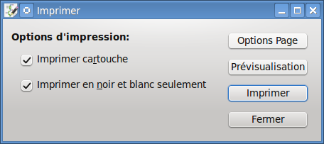
L’option "Imprimer cartouche" active ou désactive l’impression du cartouche.
L’option "Imprimer en noir et blanc seulement" force l’impression en monochrome. Cette option est généralement nécessaire si vous avez une imprimante laser noir et blanc, parce que les couleurs, imprimées en demi-tons, ne sont souvent pas très lisibles.
Symbol Library Editor
General Information About Symbol Libraries
A symbol is a schematic element which contains a graphical representation, electrical connections, and fields defining the symbol. Symbols used in a schematic are stored in symbol libraries. Eeschema provides a symbol library editing tool that allows you to create libraries, add, delete or transfer symbols between libraries, export symbols to files, and import symbols from files. The library editing tool provides a simple way to manage symbol library files.
Symbol Library Overview
A symbol library is composed of one or more symbols. Generally the symbols are logically grouped by function, type, and/or manufacturer.
A symbol is composed of:
-
Des éléments graphiques (lignes, cercles, arcs, textes, etc…), qui fournissent la définition du symbole.
-
Des broches (pins), qui ont à la fois des propriétés graphiques (ligne, horloge, inversée, active à l’état bas, etc..), et des propriétés électriques (entrée, sortie, bidirectionnelle, etc..), qui sont utilisées par l’outil de vérification des règles électriques (ERC).
-
Des champs : référence, valeur, empreintes correspondantes pour le dessin du circuit imprimé, etc…
-
Aliases used to associate a common symbol such as a 7400 with all of its derivatives such as 74LS00, 74HC00, and 7437. All of these aliases share the same library symbol.
Proper symbol designing requires:
-
Defining if the symbol is made up of one or more units.
-
Defining if the symbol has an alternate body style also known as a De Morgan representation.
-
De dessiner sa représentation symbolique, au moyen de lignes, rectangles, cercles, polygones, et de texte.
-
D’ajouter des pins, en définissant leurs éléments graphiques, leurs noms, leurs numéros et leurs propriétés électriques (entrées, sorties, trois-états, alimentations, etc..).
-
Adding an alias if other symbols have the same design and pin out or removing one if the symbol has been created from another symbol.
-
D’ajouter des champs supplémentaires, comme le nom de l’empreinte utilisée par le logiciel de dessin du circuit imprimé, et de définir leur visibilité.
-
Documenting the symbol by adding a description string and links to data sheets, etc.
-
De le sauvegarder dans la librairie désirée.
Symbol Library Editor Overview
The symbol library editor main window is shown below. It consists of three tool bars for quick access to common features and a symbol viewing/editing area. Not all commands are available on the tool bars but can be accessed using the menus.
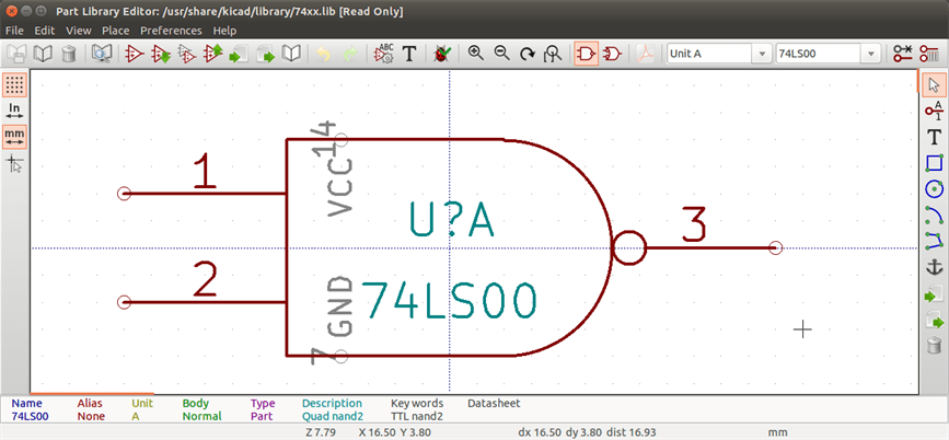
Barre d’outils principale
The main tool bar typically located at the top of the main window shown below consists of the library management tools, undo/redo commands, zoom commands, and symbol properties dialogs.

|
Save the currently selected library. The button will be disabled if no library is currently selected or no changes to the currently selected library have been made. |
|
Select the library to edit. |
|
Delete a symbol from the currently selected library or any library defined by the project if no library is currently selected. |
|
Open the symbol library browser to select the library and symbol to edit. |
|
Create a new symbol. |
|
Load symbol from currently selected library for editing. |
|
Create a new symbol from the currently loaded symbol. |
|
Save the current symbol changes in memory. The library file is not changed. |
|
Import one symbol from a file. |
|
Export the current symbol to a file. |
|
Create a new library file containing the current symbol. Note: new libraries are not automatically added to the project. |
|
Undo last edit. |
|
Redo last undo. |
|
Edit the current symbol properties. |
|
Edit the fields of current symbol. |
|
Test the current symbol for design errors. |
|
Zoom in. |
|
Zoom out. |
|
Refresh display. |
|
Zoom to fit symbol in display. |
|
Select the normal body style. The button is disabled if the current symbol does not have an alternate body style. |
|
Select the alternate body style. The button is disabled if the current symbol does not have an alternate body style. |
|
Show the associated documentation. The button will be disabled if no documentation is defined for the current symbol. |
|
Select the unit to display. The drop down control will be disabled if the current symbol is not derived from multiple units. |
|
Select the alias. The drop down control will be disabled if the current symbol does not have any aliases. |
|
Pin editing: independent editing for pin shape and position for symbols with multiple units and alternate symbols. |
|
Show pin table. |
Barre d’outils des éléments
The vertical toolbar typically located on the right hand side of the main window allows you to place all of the elements required to design a symbol. The table below defines each toolbar button.
|
Select tool. Right-clicking with the select tool opens the context menu for the object under the cursor. Left-clicking with the select tool displays the attributes of the object under the cursor in the message panel at the bottom of the main window. Double-left-clicking with the select tool will open the properties dialog for the object under the cursor. |
|
Pin tool. Left-click to add a new pin. |
|
Graphical text tool. Left-click to add a new graphical text item. |
|
Rectangle tool. Left-click to begin drawing the first corner of a graphical rectangle. Left-click again to place the opposite corner of the rectangle. |
|
Circle tool. Left-click to begin drawing a new graphical circle from the center. Left-click again to define the radius of the circle. |
|
Arc tool. Left-click to begin drawing a new graphical arc item from the center. Left-click again to define the first arc end point. Left-click again to define the second arc end point. |
|
Polygon tool. Left-click to begin drawing a new graphical polygon item in the current symbol. Left-click for each addition polygon line. Double-left-click to complete the polygon. |
|
Anchor tool. Left-click to set the anchor position of the symbol. |
|
Import a symbol from a file. |
|
Export the current symbol to a file. |
|
Delete tool. Left-click to delete an object from the current symbol. |
Barre d’outils des options
La barre d’outil verticale située à gauche de la fenêtre vous permet de régler quelques options de dessin. La table ci-dessous décrit les fonctions des différents boutons :
|
Toggle grid visibility on and off. |
|
Set units to inches. |
|
Set units to millimeters. |
|
Toggle full screen cursor on and off. |
Sélection et gestion des librairies
The selection of the current library is possible via the ![]() which shows you all available libraries and allows you to select one. When a symbol is loaded or saved, it will be put in this library. The library name of symbol is the contents of its value field.
which shows you all available libraries and allows you to select one. When a symbol is loaded or saved, it will be put in this library. The library name of symbol is the contents of its value field.
|
Select and Save a Symbol
When you edit a symbol you are not really working on the symbol in its library but on a copy of it in the computer’s memory. Any edit action can be undone easily. A symbol may be loaded from a local library or from an existing symbol.
Symbol Selection
Clicking the ![]() on the main tool bar displays the list of the available symbols that you can select and load from the currently selected library.
on the main tool bar displays the list of the available symbols that you can select and load from the currently selected library.
If a symbol is selected by its alias, the name of the loaded symbol is displayed on the window title bar instead of the selected alias. The list of symbol aliases is always loaded with each symbol and can be edited. You can create a new symbol by selecting an alias of the current symbol from the  . The first item in the alias list is the root name of the symbol. . The first item in the alias list is the root name of the symbol.
|
|
Alternatively, clicking the |
Save a Symbol
After modification, a symbol can be saved in the current library, in a new library, or exported to a backup file.
To save the modified symbol in the current library, click the ![]() . Please note that the update command only saves the symbol changes in the local memory. This way, you can make up your mind before you save the library.
. Please note that the update command only saves the symbol changes in the local memory. This way, you can make up your mind before you save the library.
To permanently save the symbol changes to the library file, click the ![]() which will overwrite the existing library file with the symbol changes.
which will overwrite the existing library file with the symbol changes.
If you want to create a new library containing the current symbol, click the ![]() . You will be asked to enter a new library name.
. You will be asked to enter a new library name.
|
Les nouvelles librairies ne sont pas automatiquement ajoutées au projet en cours. You must add any new library you wish to use in a schematic to the list of project libraries in Eeschema using the Symbol Library Table dialog. |
Click the ![]() to create a file containing only the current symbol. This file will be a standard library file which will contain only one symbol. This file can be used to import the symbol into another library. In fact, the create new library command and the export command are basically identical.
to create a file containing only the current symbol. This file will be a standard library file which will contain only one symbol. This file can be used to import the symbol into another library. In fact, the create new library command and the export command are basically identical.
Transfer Symbols to Another Library
You can very easily copy a symbol from a source library into a destination library using the following commands:
-
Choisissez la librairie d’origine par le bouton
 .
. -
Load the symbol to be transferred by clicking the
 . The symbol will be displayed in the editing area.
 -
Choisissez la librairie de destination en cliquant à nouveau sur
. -
Save the current symbol to the new library in the local memory by clicking the
 .
. -
Save the symbol in the current local library file by clicking the
 .
.
Discarding Symbol Changes
When you are working on a symbol, the edited symbol is only a working copy of the actual symbol in its library. This means that as long as you have not saved it, you can just reload it to discard all changes made. If you have already updated it in the local memory and you have not saved it to the library file, you can always quit and start again. Eeschema will undo all the changes.
Creating Library Symbols
Create a New Symbol
A new symbol can be created by clicking the ![]() . You will be asked for a symbol name (this name is used as default value for the value field in the schematic editor), the reference designator (U, IC, R…), the number of units per package (for example a 7400 is made of 4 units per package) and if an alternate body style (sometimes referred to as DeMorgan) is desired. If the reference designator field is left empty, it will default to "U". These properties can be changed later, but it is preferable to set them correctly at the creation of the symbol.
. You will be asked for a symbol name (this name is used as default value for the value field in the schematic editor), the reference designator (U, IC, R…), the number of units per package (for example a 7400 is made of 4 units per package) and if an alternate body style (sometimes referred to as DeMorgan) is desired. If the reference designator field is left empty, it will default to "U". These properties can be changed later, but it is preferable to set them correctly at the creation of the symbol.
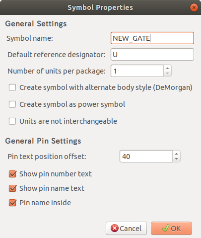
A new symbol will be created using the properties above and will appear in the editor as shown below.
Create a Symbol from Another Symbol
Often, the symbol that you want to make is similar to one already in a symbol library. In this case it is easy to load and modify an existing symbol.
-
Load the symbol which will be used as a starting point.
-
Click on the
 or modify its name by right-clicking on the value field and editing the text. If you chose to duplicate the current symbol, you will be prompted for a new symbol name.
 -
If the model symbol has aliases, you will be prompted to remove aliases from the new symbol which conflict with the current library. If the answer is no the new symbol creation will be aborted. Symbol libraries cannot have any duplicate names or aliases.
-
Edit the new symbol as required.
-
Update the new symbol in the current library by clicking the
or save to a new library by clicking the  or if you want to save this new symbol in an other existing library select the other library by clicking on the and save the new symbol.
 -
Sauvez la librairie courante sur le disque en cliquant sur
.
Symbol Properties
Symbol properties should be carefully set during the symbol creation or alternatively they are inherited from the copied symbol. To change the symbol properties, click on the ![]() to show the dialog below.
to show the dialog below.
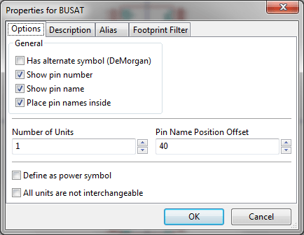
It is very important to correctly set the number of units per package and the alternate symbolic representation, if enabled, because when pins are edited or created the corresponding pins for each unit will be affected. If you change the number of units per package after pin creation and editing, there will be additional work to add the new unit pins and symbols. Nevertheless, it is possible to modify these properties at any time.
The graphic options "Show pin number" and "Show pin name" define the visibility of the pin number and pin name text. This text will be visible if the corresponding options are checked. The option "Place pin names inside" defines the pin name position relative to the pin body. This text will be displayed inside the symbol outline if the option is checked. In this case the "Pin Name Position Offset" property defines the shift of the text away from the body end of the pin. A value from 30 to 40 (in 1/1000 inch) is reasonable.
The example below shows a symbol with the "Place pin name inside" option unchecked. Notice the position of the names and pin numbers.
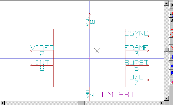
Symbols with Alternate Symbolic Representation
If the symbol has more than one symbolic repersentation, you will have to select one representation to edit them. To edit the normal representation, click the ![]() .
.
To edit the alternate representation, click on the ![]() . Use the shown below to select the unit you wish to edit.
. Use the shown below to select the unit you wish to edit.
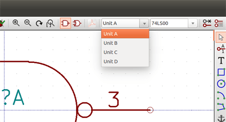
Éléments graphiques
Graphical elements create the representation of a symbol and contain no electrical connection information. Their design is possible using the following tools:
-
Lignes et polygones définis par des points d’origine et des points de fin.
-
Rectangles définis par leurs deux coins opposés sur la diagonale.
-
Cercles définis par leur centre et leur rayon.
-
Arcs de cercles définis par leur centre et leurs points de départ et de fin. Un arc peut aller de 0 à 180°.
The vertical toolbar on the right hand side of the main window allows you to place all of the graphical elements required to design the representation of a symbol.
Appartenance des éléments graphiques
Chaque élément graphique, (ligne, arc, cercle, etc…), peut être défini comme commun à toutes les unités et/ou représentations, ou spécifique à une unité donnée et/ou une représentation. Les options des éléments sont accessibles rapidement par le menu contextuel : clic droit sur l’élément à modifier. Ci-dessous, le menu contextuel pour un élément de type ligne.
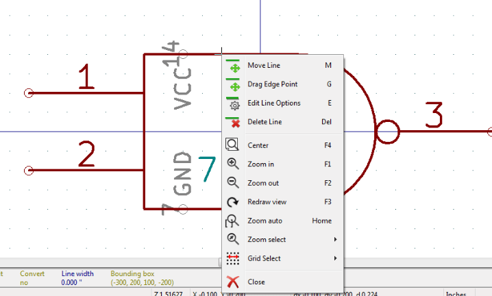
Vous pouvez aussi double-cliquer sur un élément et modifier ses propriétés. Ci-dessous, la fenêtre des propriétés pour un élément de type polygone.
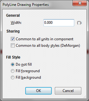
Les propriétés d’un élément graphique sont :
-
La largeur de ligne de l’élément dans l’unité courante.
-
The "Common to all units in symbol" setting defines if the graphical element is drawn for each unit in symbol with more than one unit per package or if the graphical element is only drawn for the current unit.
-
The "Common by all body styles (DeMorgan)" setting defines if the graphical element is drawn for each symbolic representation in symbols with an alternate body style or if the graphical element is only drawn for the current body style.
-
Les options de "Style de remplissage" déterminent si le symbole défini par l’élément graphique doit être vide, rempli avec la couleur de premier plan, ou rempli avec la couleur de fond.
Éléments Graphiques Textes
The ![]() allows for the creation of graphical text. Graphical text is always readable, even when the symbol is mirrored. Please note that graphical text items are not fields.
allows for the creation of graphical text. Graphical text is always readable, even when the symbol is mirrored. Please note that graphical text items are not fields.
Multiple Units per Symbol and Alternate Body Styles
Symbols can have two symbolic representations (a standard symbol and an alternate symbol often referred to as "DeMorgan") and/or have more than one unit per package (logic gates for example). Some symbols can have more than one unit per package each with different symbols and pin configurations.
Consider for instance a relay with two switches which can be designed as a symbol with three different units: a coil, switch 1, and switch 2. Designing a symbol with multiple units per package and/or alternate body styles is very flexible. A pin or a body symbol item can be common to all units or specific to a given unit or they can be common to both symbolic representation so are specific to a given symbol representation.
Par défaut, les pins sont spécifiques à chaque représentation symbolique de chaque unité, parce que le numéro de pin est spécifique à une unité, et sa forme dépend de la représentation symbolique. Quand une pin est commune à chaque unité ou chaque représentation symbolique, vous n’avez besoin de la créer qu’une seule fois pour toutes les unités et toutes les représentations symboliques (ce qui est généralement le cas pour les pins d’alimentation). C’est également le cas pour la forme de l’unité et le texte, qui peuvent être communs à chaque unité (mais généralement sont spécifiques à chaque représentation symbolique).
Example of a Symbol Having Multiple Units with Different Symbols:
Voici l’exemple d’un relais contenant 3 unités, la bobine, le switch 1 et le switch 2 :
Le bouton "Éditer pins unité par unité ou forme par forme" permet d’ajouter ou d’éditer des pins pour chaque unité sans aucun lien avec les pins des autres unités.
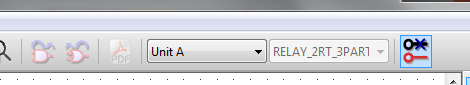
l’option "Toutes les unités ne sont pas interchangeables", des propriétés du composant, doit être cochée.
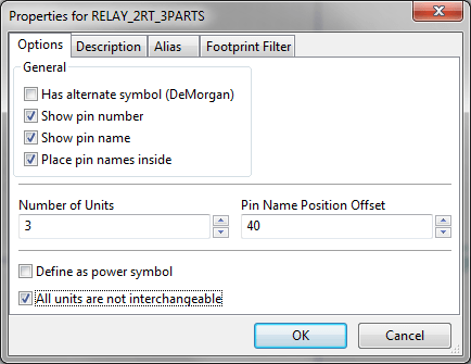
Unité 1
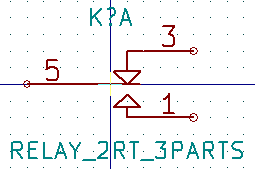
Unité 2
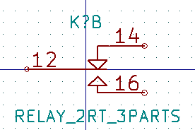
Unité 3
L’unité 3 n’a pas le même symbole, ni les mêmes pins, et du fait, n’est pas interchangeable avec les unités 1 et 2.
Éléments graphiques symboliques
Shown below are properties for a graphic body element. From the relay example above, the three units have different symbolic representations. Therefore, each unit was created separately and the graphical body elements must have the "Common to all units in symbol" disabled.
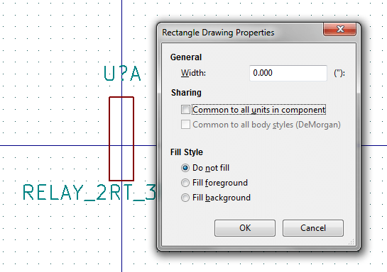
Création et édition de pins
Cliquez sur ![]() pour créer et insérer une pin. L’édition de ses propriétés se fait par un double-clic sur la pin ou par un clic droit pour ouvrir son menu contextuel. Les pins doivent être créées avec soin, car toute erreur aura des conséquences sur le dessin du PCB. Toute pin déjà placée peut être modifiée, supprimée, et / ou déplacée.
pour créer et insérer une pin. L’édition de ses propriétés se fait par un double-clic sur la pin ou par un clic droit pour ouvrir son menu contextuel. Les pins doivent être créées avec soin, car toute erreur aura des conséquences sur le dessin du PCB. Toute pin déjà placée peut être modifiée, supprimée, et / ou déplacée.
Généralités sur les pins
Une pin est définie par sa représentation graphique, son nom et son "numéro". Le "numéro" de pin est défini par un ensemble de 4 lettres et / ou chiffres. Pour que l’outil de vérification des règles électriques (ERC) soit utile, le type "électrique" de la pin (entrée, sortie, trois-états, …) doit être défini avec le plus grand soin. Si ce type n’est pas défini correctement, le résultat de la vérification du schéma peut être invalide.
Notes importantes :
-
N’utilisez pas d’espaces dans les noms et les numéros de pins.
-
Pour définir un nom de pin avec un signal inversé (barre au-dessus), utilisez le caractère “~” (tilde). Le caractère “~” suivant terminera la barre. Par exemple : ~FO~O` affichera FO O.
-
Si le nom d’une pin est réduit à un seul caractère symbolique, la pin est considérée comme non-nommée.
-
Les noms de pins commençant par “#”, sont réservés aux symboles d’alimentations.
-
Un "numéro" de pin contient de 1 à 4 lettres et/ou chiffres. 1,2,..9999 sont valides. A1, B3, Anod, Gnd, Wire, etc… sont valides également.
-
Duplicate pin "numbers" cannot exist in a symbol.
Propriétés des pins
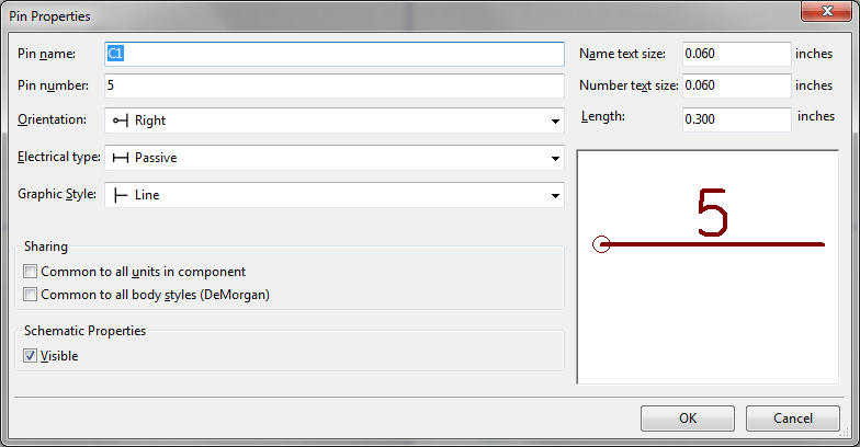
La fenêtre des propriétés des pins vous permet de modifier toutes les caractéristiques d’une pin. Cette fenêtre apparaît automatiquement à la création de la pin ou quand vous double-cliquez sur une pin existante. Vous pouvez modifier :
-
Son nom et la dimension de son nom.
-
Son numéro et la dimension de son numéro.
-
Son orientation et sa longueur.
-
Son type électrique et son style graphique.
-
Son appartenance aux unités et aux représentations alternatives.
-
Sa visibilité.
Styles graphiques des pins
Ci-dessous, les différents styles de pins. Le choix du style n’a aucune influence sur le type électrique de la pin.
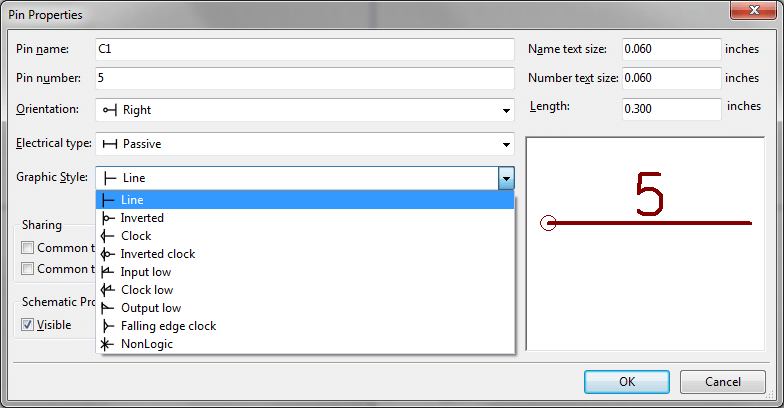
Types électriques des pins
Choisir le type électrique correct est important pour l’outil de vérification (ERC). Les types électriques sont :
-
Bidirectionel : pin pouvant être alternativement une entrée ou une sortie (bus de données de microprocesseur, par exemple).
-
Trois-états : type classique d’une sortie trois-états.
-
Passive is used for passive symbol pins, resistors, connectors, etc.
-
Non-Spécifié : sera utilisé quand sa vérification par l’ERC n’est pas importante.
-
Power input is used for the symbol’s power pins. Power pins are automatically connected to the other power input pins with the same name.
-
Power output : utilisé pour les sorties de régulateurs de tension.
-
Collecteur ouvert et Émetteur ouvert : pour les sorties logiques définies comme telles.
-
Not connected is used when a symbol has a pin that has no internal connection.
Propriétés globales des pins
You can modify the length or text size of the name and/or number of all the pins using the Global command entry of the pin context menu. Click on the parameter you want to modify and type the new value which will then be applied to all of the current symbol’s pins.
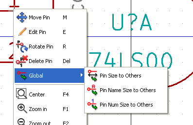
Définitions de pins pour unités multiples et représentations alternatives
Symbols with multiple units and/or graphical representations are particularly problematic when creating and editing pins. The majority of pins are specific to each unit (because their pin number is specific to each unit) and to each symbolic representation (because their form and position is specific to each symbolic representation). The creation and the editing of pins can be problematic for symbols with multiple units per package and alternate symbolic representations. The symbol library editor allows the simultaneous creation of pins. By default, changes made to a pin are made for all units of a multiple unit symbol and both representations for symbols with an alternate symbolic representation.
La seule exception à ceci concerne son type graphique et son nom. Cette limitation a été faite pour faciliter la création et l’édition de pins dans la plupart des cas. Cette limitation peut être désactivée en basculant l’option ![]() sur la barre d’outils principale. Ceci vous permettra de créer des pins pour chaque unité et chaque représentation de façon complètement indépendante.
sur la barre d’outils principale. Ceci vous permettra de créer des pins pour chaque unité et chaque représentation de façon complètement indépendante.
A symbol can have two symbolic representations (representation known as``DeMorgan'') and can be made up of more than one unit as in the case of symbols with logic gates. For certain symbols, you may want several different graphic elements and pins. Like the relay sample shown in the previous section, a relay can be represented by three distinct units: a coil, switch contact 1, and switch contact 2.
The management of the symbols with multiple units and symbols with alternate symbolic representations is flexible. A pin can be common or specific to different units. A pin can also be common to both symbolic representations or specific to each symbolic representation.
Par défaut, les pins sont spécifiques à chaque représentation de chaque unité, car leur numéro diffère pour chaque unité, et leur dessin est différent pour chaque représentation symbolique. Quand une pin est commune à toutes les unités, comme par exemple dans le cas des pins d’alimentation, elle ne doit être dessinée qu’une fois.
An example is the output pin 7400 quad dual input NAND gate. Since there are four units and two symbolic representations, there are eight separate output pins defined in the symbol definition. When creating a new 7400 symbol, unit A of the normal symbolic representation will be shown in the library editor. To edit the pin style in alternate symbolic representation, it must first be enabled by clicking the ![]() button on the tool bar. To edit the pin number for each unit, select the appropriate unit using the drop down control.
button on the tool bar. To edit the pin number for each unit, select the appropriate unit using the drop down control.
Symbol Fields
All library symbols are defined with four default fields. The reference designator, value, footprint assignment, and documentation file link fields are created whenever a symbol is created or copied. Only the reference designator and value fields are required. For existing fields, you can use the context menu commands by right-clicking on the pin. Symbols defined in libraries are typically defined with these four default fields. Additional fields such as vendor, part number, unit cost, etc. can be added to library symbols but generally this is done in the schematic editor so the additional fields can be applied to all of the symbols in the schematic.
Editing Symbol Fields
To edit an existing symbol field, right-click on the field text to show the field context menu shown below.
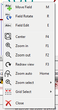
To edit undefined fields, add new fields, or delete optional fields ![]() on the main tool bar to open the field properties dialog shown below.
on the main tool bar to open the field properties dialog shown below.
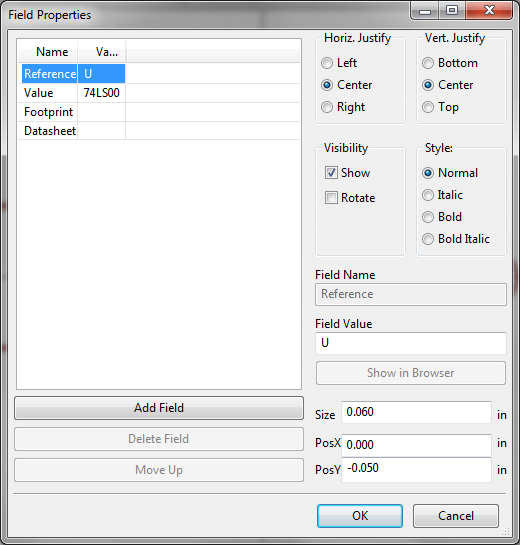
Fields are text sections associated with the symbol. Do not confuse them with the text belonging to the graphic representation of this symbol.
Notes importantes :
-
Modifying value fields effectively creates a new symbol using the current symbol as the starting point for the new symbol. This new symbol has the name contained in the value field when you save it to the currently selected library.
-
The field edit dialog above must be used to edit a field that is empty or has the invisible attribute enabled.
-
L’empreinte associée est définie de façon absolue en utilisant le format LIBNAME:FPNAME, où LIBNAME est le nom de la librairie de l’empreinte défini dans la table des librairies d’empreintes (voir la section "Table des librairies d’empreintes" du "Manuel de référence" de Pcbnew), et FPNAME le nom de l’empreinte dans la bibliothèque LIBNAME.
Symboles d’alimentation
Power symbols are created the same way as normal symbols. It may be useful to place them in a dedicated library such as power.lib. Power symbols consist of a graphical symbol and a pin of the type "Power Invisible". Power port symbols are handled like any other symbol by the schematic capture software. Some precautions are essential. Below is an example of a power +5V symbol.
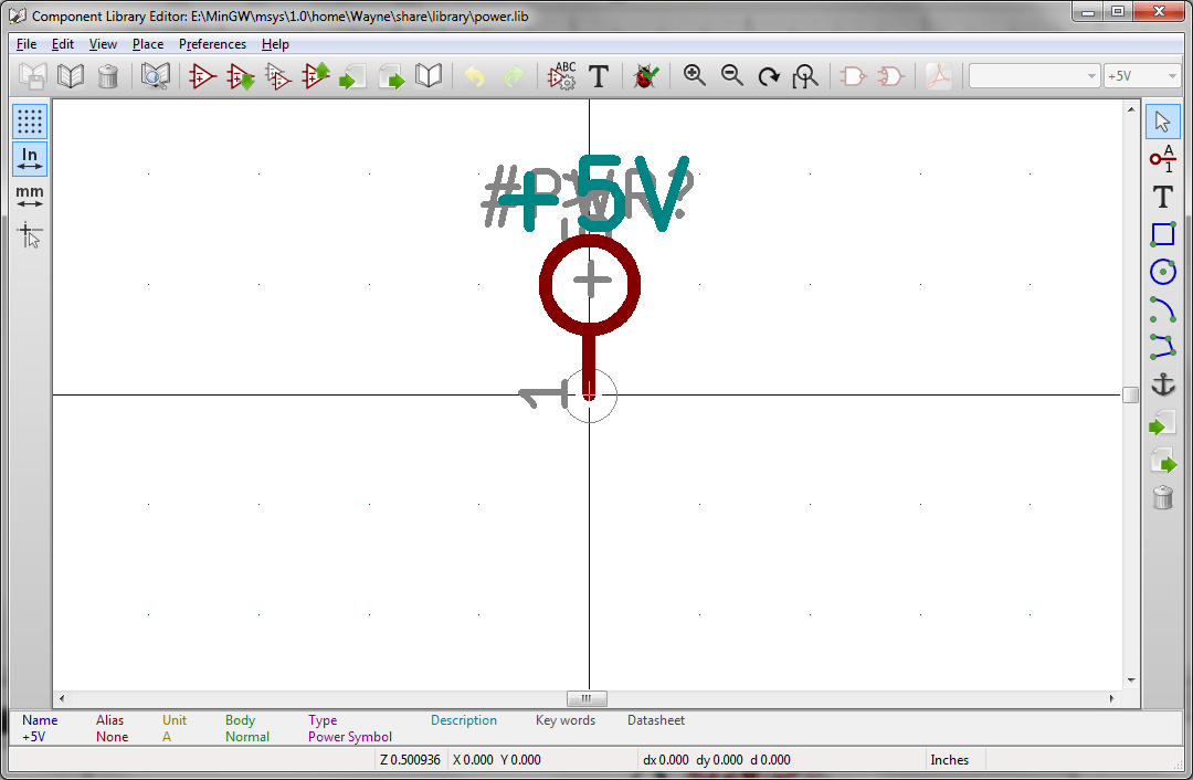
Pour créer un symbole d’alimentation, utilisez les étapes suivantes :
-
Ajouter une pin de type "Power Input", avec pour nom +5V (important parce que ce nom va établir la connexion au net +5V), un numéro de pin à 1 (ce numéro n’a aucune importance), une longueur de 0, et comme Style graphique : "ligne".
-
Placez un petit cercle et un segment graphique, de la pin au cercle, comme indiqué.
-
Le point d’ancrage du symbole est sur la pin.
-
The symbol value is
+5V. -
The symbol reference is
#+5V. The reference text is not important except the first character which must be#to indicate that the symbol is a power symbol. By convention, every symbol in which the reference field starts with a#will not appear in the symbol list or in the netlist and the reference is declared as invisible.
Une méthode plus facile pour créer un nouveau symbole d’alimentation est d’utiliser un autre symbole comme modèle :
-
Chargez un symbole d’alimentation.
-
Éditez le nom de la pin du nouveau symbole.
-
Donnez au champ valeur le même nom que la pin, si vous voulez afficher la valeur de l’alimentation.
-
Save the new symbol.
LibEdit - Symbols
Généralités
A symbol consist of the following elements
-
Une représentation graphique (formes géométriques, textes).
-
Des pins.
-
Fields or associated text used by the post processors: netlist, symbols list.
Two fields are to be initialized: reference and value. The name of the design associated with the symbol, and the name of the associated footprint, the other fields are the free fields, they can generally remain empty, and could be filled during schematic capture.
However, managing the documentation associated with any symbol facilitates the research, use and maintenance of libraries. The associated documentation consists of
-
Une ligne de commentaire.
-
Une ligne de mots-clefs, séparés par des espaces, comme TTL CMOS NAND2.
-
Un nom de fichier attaché (par exemple une note d’application ou un fichier PDF).
Le répertoire par défaut des fichiers attachés :
kicad/share/library/doc
S’il n’existe pas :
kicad/library/doc
Sous Linux :
/usr/local/kicad/share/library/doc
/usr/share/kicad/library/doc
/usr/local/share/kicad/library/doc
Key words allow you to selectively search for a symbol according to various selection criteria. Comments and key words are displayed in various menus, and particularly when you select a symbol from the library.
The symbol also has an anchoring point. A rotation or a mirror is made relative to this anchor point and during a placement this point is used as a reference position. It is thus useful to position this anchor accurately.
A symbol can have aliases, i.e. equivalent names. This allows you to considerably reduce the number of symbols that need to be created (for example, a 74LS00 can have aliases such as 74000, 74HC00, 74HCT00…).
Finally, the symbols are distributed in libraries (classified by topics, or manufacturer) in order to facilitate their management.
Position a symbol anchor
Le point d’ancrage est aux coordonnées (0,0) et est représenté par les axes bleus affichés à l’écran.
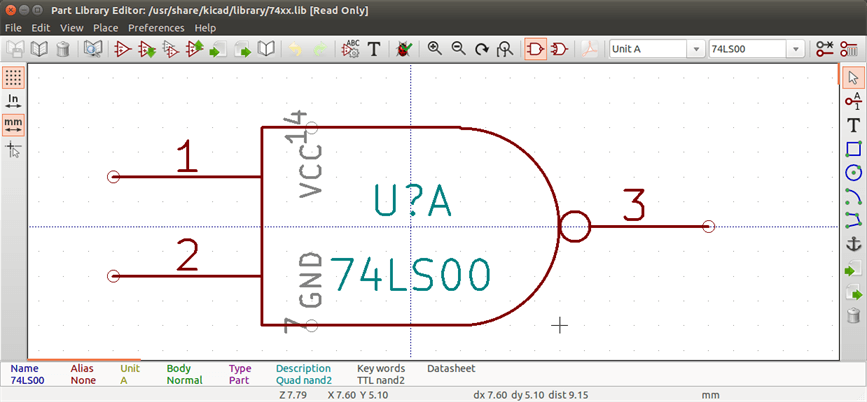
Le point d’ancrage peut être repositionné en sélectionnant l’icône ![]() et en cliquant à la nouvelle position souhaitée du point d’ancrage. Le dessin sera automatiquement recentré sur ce nouveau point d’ancrage.
et en cliquant à la nouvelle position souhaitée du point d’ancrage. Le dessin sera automatiquement recentré sur ce nouveau point d’ancrage.
Symbol aliases
An alias is another name corresponding to the same symbol in the library. Symbols with similar pin-out and representation can then be represented by only one symbol, having several aliases (e.g. 7400 with alias 74LS00, 74HC00, 74LS37 ).
L’utilisation d’alias vous permet de fabriquer rapidement des librairies entières. De plus, ces librairies, étant beaucoup plus compactes, seront plus facilement chargées par KiCad.
Pour modifier la liste des alias, vous devez sélectionner la fenêtre d’édition principale des propriétés par l’icône ![]() et sélectionnez l’onglet alias.
et sélectionnez l’onglet alias.
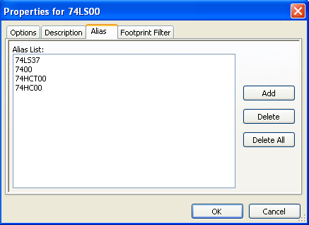
Vous pouvez ainsi ajouter ou supprimer l’alias désiré. L’alias actuel ne peut évidemment pas être supprimé puisqu’il est en cours d’édition.
To remove all aliases, you have firstly to select the root symbol. The first symbol in the alias list in the window of selection of the main toolbar.
Symbol fields
The field editor is called via the icon ![]() .
.
There are four special fields (texts attached to the symbol), and configurable user fields
Champs spéciaux
-
Référence.
-
Value. It is the symbol name in the library and the default value field in schematic.
-
Empreinte. Le nom d’empreinte qui sera utilisée sur le circuit. Pas très utile si on utilise CvPcb pour associer les empreintes, mais obligatoire si on ne l’utilise pas.
-
Datasheet. C’est un champ réservé, pas actuellement utilisé.
Symbol documentation
To edit documentation information, it is necessary to call the main editing window of the symbol via the icon ![]() and to select the document folder.
and to select the document folder.
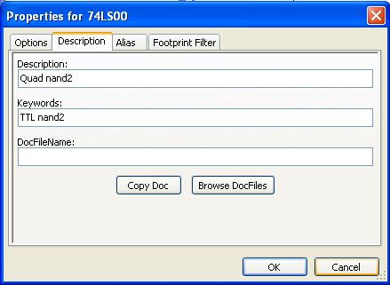
Be sure to select the right alias, or the root symbol, because this documentation is the only characteristic which differs between aliases. The "Copy Doc" button allows you to copy the documentation information from the root symbol towards the currently edited alias.
Symbol keywords
Keywords allow you to search in a selective way for a symbol according to specific selection criteria (function, technological family, etc.)
L’outil de recherche de Eeschema est insensible à la casse. Les mots-clés les plus couramment utilisés dans les librairies sont :
-
CMOS TTL pour les familles de composants logiques.
-
AND2 NOR3 XOR2 INV… pour les portes (AND2 = porte ET 2 entrées, NOR3 = porte NON-OU 3 entrées).
-
JKFF DFF… pour les bascules JK ou D.
-
ADC, DAC, MUX…
-
OpenCol for the gates with open collector output. Thus if in the schematic capture software, you search the symbol: by keywords NAND2 OpenCol Eeschema will display the list of symbols having these 2 key words.
Symbol documentation (Doc)
The line of comment (and keywords) is displayed in various menus, particularly when you select a symbol in the displayed symbols list of a library and in the ViewLib menu.
If this Doc. file exists, it is also accessible in the schematic capture software, in the pop-up menu displayed by right-clicking on the symbol.
Fichier de documentation associé (DocFileName)
Indique la disponibilité d’un fichier attaché (documentation, schéma applicatif), PDF, schéma, etc…
Filtrage d’empreintes pour CvPcb
You can enter a list of allowed footprints for the symbol. This list acts as a filter used by CvPcb to display only the allowed footprints. A void list does not filter anything.
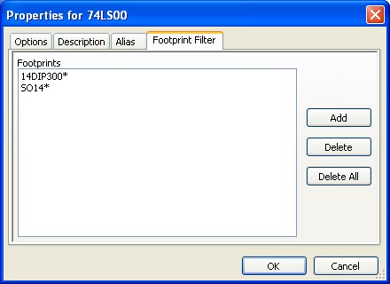
Les caractères de remplacement sont autorisés.
S014* fera afficher par CvPcb toutes les empreintes avec un nom commençant par SO14.
Pour une résistance, R? montrera les empreintes avec 2 lettres et dont le nom commence par R.
Voici quelques exemples, avec ou sans filtrage :
Avec filtrage
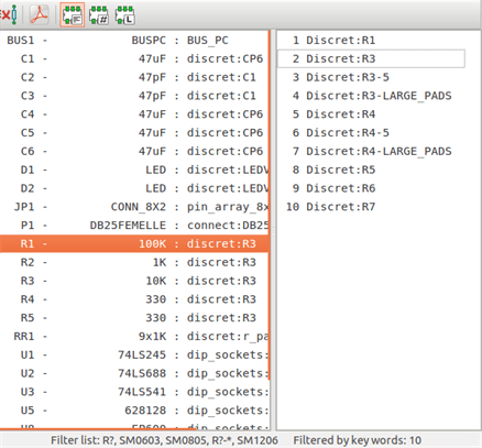
Sans filtrage
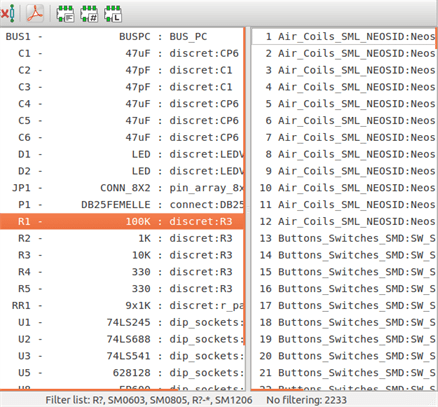
Librairie de symboles
You can easily compile a graphic symbols library file containing frequently used symbols. This can be used for the creation of symbols (triangles, the shape of AND, OR, Exclusive OR gates, etc.) for saving and subsequent re-use.
These files are stored by default in the library directory and have a '.sym' extension. These symbols are not gathered in libraries like the normal symbols because they are generally not so many.
Exporter ou créer un symbole
A symbol can be exported with the button ![]() . You can generally create only one graphic, also it will be a good idea to delete all pins, if they exist.
. You can generally create only one graphic, also it will be a good idea to delete all pins, if they exist.
Importer un symbole
Importing allows you to add graphics to a symbol you are editing. A symbol is imported with the button ![]() . Imported graphics are added as they were created in existing graphics.
. Imported graphics are added as they were created in existing graphics.
Symbol Library Browser
Introduction
The Symbol Library Browser allows you to quickly examine the content of symbol libraries. The Symbol Library Viewer can be accessed by clicking ![]() icon on the main toolbar, selecting "Library Browser" entry in the "View" menu or double clicking symbol image on "Choose Symbol" window.
icon on the main toolbar, selecting "Library Browser" entry in the "View" menu or double clicking symbol image on "Choose Symbol" window.
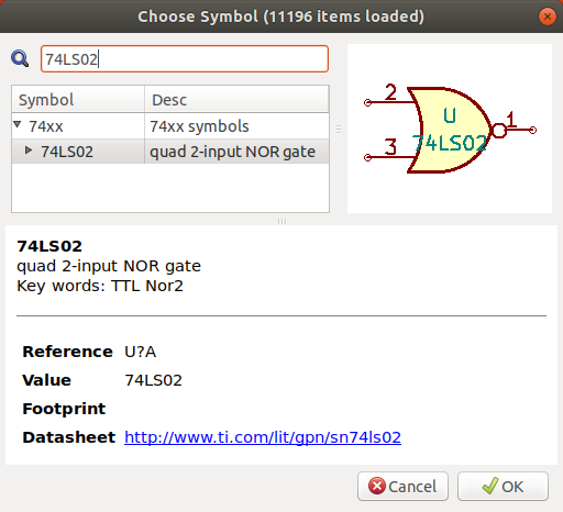
Viewlib - fenêtre principale
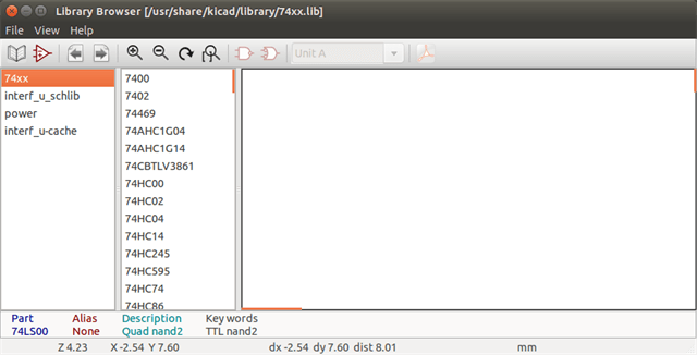
To examine the contents of a library, select a library from the list on the left hand pane. All symbols in the selected library will appear in the second pane. Select a symbol name to view the symbol.
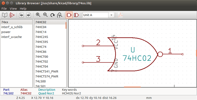
Symbol Library Browser Top Toolbar
The top tool bar in Symbol Library Brower is shown below.

The available commands are:
|
Selection of the desired library which can be also selected in the displayed list. |
|
Selection of the symbol which can be also selected in the displayed list. |
|
Display previous symbol. |
|
Display next symbol. |
|
Zoom tools. |
|
Selection of the representation (normal or converted) if exist. |
|
Selection of the unit for symbols that contain multiple units. |
|
If it exist, display the associated documents. Exists only when called by the place symbol dialog frame from Eeschema. |
|
Close the browser and place the selected symbol in Eeschema. This icon is only displayed when browser has been called from Eeschema (double click on a symbol in the component chooser). |

Création de Netlistes et BOM personnalisés
Fichier intermédiaire de Netliste
Les fichiers de BOM et de Netlistes sont convertis à partir d’un fichier intermédiaire créé par Eeschema.
Ce fichier utilise une syntaxe XML, et est appelé "netliste intermédiaire". Cette netliste intermédiaire inclue une grande quantité de données relatives au circuit, et, pour cette raison, il peut être utilisé par un post-traitement pour créer une liste de composants ou d’autres rapports.
Suivant le fichier de sortie (BOM ou netliste), différentes portions de la netliste intermédiaire seront utilisées dans le post-traitement.
Exemple de schéma
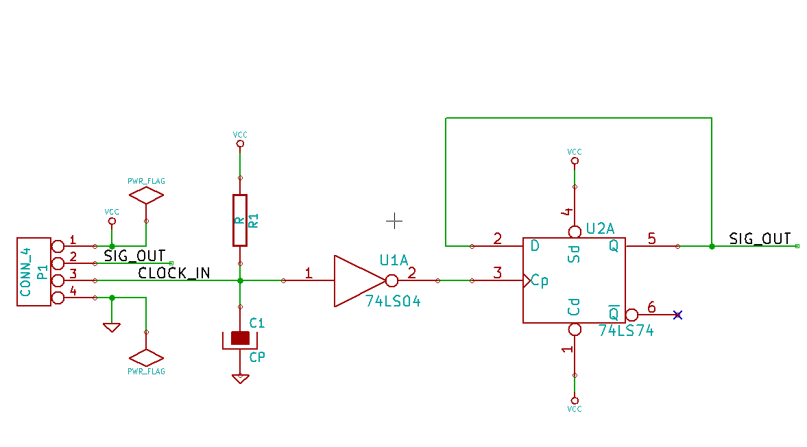
Exemple de fichier netliste intermédiaire
Le fichier netliste intermédiaire (utilisant une syntaxe XML) correspondant au schéma ci-dessus :
<?xml version="1.0" encoding="utf-8"?>
<export version="D">
<design>
<source>F:\kicad_aux\netlist_test\netlist_test.sch</source>
<date>29/08/2010 20:35:21</date>
<tool>eeschema (2010-08-28 BZR 2458)-unstable</tool>
</design>
<components>
<comp ref="P1">
<value>CONN_4</value>
<libsource lib="conn" part="CONN_4"/>
<sheetpath names="/" tstamps="/"/>
<tstamp>4C6E2141</tstamp>
</comp>
<comp ref="U2">
<value>74LS74</value>
<libsource lib="74xx" part="74LS74"/>
<sheetpath names="/" tstamps="/"/>
<tstamp>4C6E20BA</tstamp>
</comp>
<comp ref="U1">
<value>74LS04</value>
<libsource lib="74xx" part="74LS04"/>
<sheetpath names="/" tstamps="/"/>
<tstamp>4C6E20A6</tstamp>
</comp>
<comp ref="C1">
<value>CP</value>
<libsource lib="device" part="CP"/>
<sheetpath names="/" tstamps="/"/>
<tstamp>4C6E2094</tstamp>
</comp>
<comp ref="R1">
<value>R</value>
<libsource lib="device" part="R"/>
<sheetpath names="/" tstamps="/"/>
<tstamp>4C6E208A</tstamp>
</comp>
</components>
<libparts>
<libpart lib="device" part="C">
<description>Condensateur non polarise</description>
<footprints>
<fp>SM*</fp>
<fp>C?</fp>
<fp>C1-1</fp>
</footprints>
<fields>
<field name="Reference">C</field>
<field name="Value">C</field>
</fields>
<pins>
<pin num="1" name="~" type="passive"/>
<pin num="2" name="~" type="passive"/>
</pins>
</libpart>
<libpart lib="device" part="R">
<description>Resistance</description>
<footprints>
<fp>R?</fp>
<fp>SM0603</fp>
<fp>SM0805</fp>
<fp>R?-*</fp>
<fp>SM1206</fp>
</footprints>
<fields>
<field name="Reference">R</field>
<field name="Value">R</field>
</fields>
<pins>
<pin num="1" name="~" type="passive"/>
<pin num="2" name="~" type="passive"/>
</pins>
</libpart>
<libpart lib="conn" part="CONN_4">
<description>Symbole general de connecteur</description>
<fields>
<field name="Reference">P</field>
<field name="Value">CONN_4</field>
</fields>
<pins>
<pin num="1" name="P1" type="passive"/>
<pin num="2" name="P2" type="passive"/>
<pin num="3" name="P3" type="passive"/>
<pin num="4" name="P4" type="passive"/>
</pins>
</libpart>
<libpart lib="74xx" part="74LS04">
<description>Hex Inverseur</description>
<fields>
<field name="Reference">U</field>
<field name="Value">74LS04</field>
</fields>
<pins>
<pin num="1" name="~" type="input"/>
<pin num="2" name="~" type="output"/>
<pin num="3" name="~" type="input"/>
<pin num="4" name="~" type="output"/>
<pin num="5" name="~" type="input"/>
<pin num="6" name="~" type="output"/>
<pin num="7" name="GND" type="power_in"/>
<pin num="8" name="~" type="output"/>
<pin num="9" name="~" type="input"/>
<pin num="10" name="~" type="output"/>
<pin num="11" name="~" type="input"/>
<pin num="12" name="~" type="output"/>
<pin num="13" name="~" type="input"/>
<pin num="14" name="VCC" type="power_in"/>
</pins>
</libpart>
<libpart lib="74xx" part="74LS74">
<description>Dual D FlipFlop, Set & Reset</description>
<docs>74xx/74hc_hct74.pdf</docs>
<fields>
<field name="Reference">U</field>
<field name="Value">74LS74</field>
</fields>
<pins>
<pin num="1" name="Cd" type="input"/>
<pin num="2" name="D" type="input"/>
<pin num="3" name="Cp" type="input"/>
<pin num="4" name="Sd" type="input"/>
<pin num="5" name="Q" type="output"/>
<pin num="6" name="~Q" type="output"/>
<pin num="7" name="GND" type="power_in"/>
<pin num="8" name="~Q" type="output"/>
<pin num="9" name="Q" type="output"/>
<pin num="10" name="Sd" type="input"/>
<pin num="11" name="Cp" type="input"/>
<pin num="12" name="D" type="input"/>
<pin num="13" name="Cd" type="input"/>
<pin num="14" name="VCC" type="power_in"/>
</pins>
</libpart>
</libparts>
<libraries>
<library logical="device">
<uri>F:\kicad\share\library\device.lib</uri>
</library>
<library logical="conn">
<uri>F:\kicad\share\library\conn.lib</uri>
</library>
<library logical="74xx">
<uri>F:\kicad\share\library\74xx.lib</uri>
</library>
</libraries>
<nets>
<net code="1" name="GND">
<node ref="U1" pin="7"/>
<node ref="C1" pin="2"/>
<node ref="U2" pin="7"/>
<node ref="P1" pin="4"/>
</net>
<net code="2" name="VCC">
<node ref="R1" pin="1"/>
<node ref="U1" pin="14"/>
<node ref="U2" pin="4"/>
<node ref="U2" pin="1"/>
<node ref="U2" pin="14"/>
<node ref="P1" pin="1"/>
</net>
<net code="3" name="">
<node ref="U2" pin="6"/>
</net>
<net code="4" name="">
<node ref="U1" pin="2"/>
<node ref="U2" pin="3"/>
</net>
<net code="5" name="/SIG_OUT">
<node ref="P1" pin="2"/>
<node ref="U2" pin="5"/>
<node ref="U2" pin="2"/>
</net>
<net code="6" name="/CLOCK_IN">
<node ref="R1" pin="2"/>
<node ref="C1" pin="1"/>
<node ref="U1" pin="1"/>
<node ref="P1" pin="3"/>
</net>
</nets>
</export>
Conversion dans un nouveau format de netliste
En appliquant un filtre de post-traitement au fichier netliste Intermédiaire, vous pouvez générer des formats inconnus de netliste, ou de BOM. Parce que cette conversion est une transformation de texte en texte, ce filtre de post-traitement pourra être écrit en Python, XSLT, ou tout autre outil capable de prendre du XML en entrée.
XSLT itself is an XML language very suitable for XML transformations. There is a free program called xsltproc that you can download and install. The xsltproc program can be used to read the Intermediate XML netlist input file, apply a style-sheet to transform the input, and save the results in an output file. Use of xsltproc requires a style-sheet file using XSLT conventions. The full conversion process is handled by Eeschema, after it is configured once to run xsltproc in a specific way.
L’approche XSLT
Vous trouverez la documentation qui décrit les transformations XSL (XSLT) ici :
Créer un fichier Netliste Pads-Pcb
Le format pads-pcb contient deux sections.
-
La liste des empreintes.
-
La Netliste : qui regroupe les références des broches par équipotentielles.
Ci-dessous, une feuille de style qui convertit le fichier netliste intermédiaire au format de netliste pads-pcb
<?xml version="1.0" encoding="ISO-8859-1"?>
<!--XSL style sheet to Eeschema Generic Netlist Format to PADS netlist format
Copyright (C) 2010, SoftPLC Corporation.
GPL v2.
How to use:
https://lists.launchpad.net/kicad-developers/msg05157.html
-->
<!DOCTYPE xsl:stylesheet [
<!ENTITY nl "
"> <!--new line CR, LF -->
]>
<xsl:stylesheet version="1.0" xmlns:xsl="http://www.w3.org/1999/XSL/Transform">
<xsl:output method="text" omit-xml-declaration="yes" indent="no"/>
<xsl:template match="/export">
<xsl:text>*PADS-PCB*&nl;*PART*&nl;</xsl:text>
<xsl:apply-templates select="components/comp"/>
<xsl:text>&nl;*NET*&nl;</xsl:text>
<xsl:apply-templates select="nets/net"/>
<xsl:text>*END*&nl;</xsl:text>
</xsl:template>
<!-- for each component -->
<xsl:template match="comp">
<xsl:text> </xsl:text>
<xsl:value-of select="@ref"/>
<xsl:text> </xsl:text>
<xsl:choose>
<xsl:when test = "footprint != '' ">
<xsl:apply-templates select="footprint"/>
</xsl:when>
<xsl:otherwise>
<xsl:text>unknown</xsl:text>
</xsl:otherwise>
</xsl:choose>
<xsl:text>&nl;</xsl:text>
</xsl:template>
<!-- for each net -->
<xsl:template match="net">
<!-- nets are output only if there is more than one pin in net -->
<xsl:if test="count(node)>1">
<xsl:text>*SIGNAL* </xsl:text>
<xsl:choose>
<xsl:when test = "@name != '' ">
<xsl:value-of select="@name"/>
</xsl:when>
<xsl:otherwise>
<xsl:text>N-</xsl:text>
<xsl:value-of select="@code"/>
</xsl:otherwise>
</xsl:choose>
<xsl:text>&nl;</xsl:text>
<xsl:apply-templates select="node"/>
</xsl:if>
</xsl:template>
<!-- for each node -->
<xsl:template match="node">
<xsl:text> </xsl:text>
<xsl:value-of select="@ref"/>
<xsl:text>.</xsl:text>
<xsl:value-of select="@pin"/>
<xsl:text>&nl;</xsl:text>
</xsl:template>
</xsl:stylesheet>
Voici le fichier de sortie pads-pcb après traitement par xsltproc :
*PADS-PCB*
*PART*
P1 unknown
U2 unknown
U1 unknown
C1 unknown
R1 unknown
*NET*
*SIGNAL* GND
U1.7
C1.2
U2.7
P1.4
*SIGNAL* VCC
R1.1
U1.14
U2.4
U2.1
U2.14
P1.1
*SIGNAL* N-4
U1.2
U2.3
*SIGNAL* /SIG_OUT
P1.2
U2.5
U2.2
*SIGNAL* /CLOCK_IN
R1.2
C1.1
U1.1
P1.3

*END*
La ligne de commande utilisée pour effectuer cette conversion :
kicad\\bin\\xsltproc.exe -o test.net kicad\\bin\\plugins\\netlist_form_pads-pcb.xsl test.tmp
Créer un fichier de netliste Cadstar
Le format Cadstar contient deux sections.
-
La liste des empreintes.
-
La Netliste : qui regroupe les références des broches par équipotentielles.
Ci-dessous, la feuille de style pour effectuer cette conversion spécifique :
<?xml version="1.0" encoding="ISO-8859-1"?>
<!--XSL style sheet to Eeschema Generic Netlist Format to CADSTAR netlist format
Copyright (C) 2010, Jean-Pierre Charras.
Copyright (C) 2010, SoftPLC Corporation.
GPL v2.
<!DOCTYPE xsl:stylesheet [
<!ENTITY nl "
"> <!--new line CR, LF -->
]>
<xsl:stylesheet version="1.0" xmlns:xsl="http://www.w3.org/1999/XSL/Transform">
<xsl:output method="text" omit-xml-declaration="yes" indent="no"/>
<!-- Netlist header -->
<xsl:template match="/export">
<xsl:text>.HEA&nl;</xsl:text>
<xsl:apply-templates select="design/date"/> <!-- Generate line .TIM <time> -->
<xsl:apply-templates select="design/tool"/> <!-- Generate line .APP <eeschema version> -->
<xsl:apply-templates select="components/comp"/> <!-- Generate list of components -->
<xsl:text>&nl;&nl;</xsl:text>
<xsl:apply-templates select="nets/net"/> <!-- Generate list of nets and connections -->
<xsl:text>&nl;.END&nl;</xsl:text>
</xsl:template>
<!-- Generate line .TIM 20/08/2010 10:45:33 -->
<xsl:template match="tool">
<xsl:text>.APP "</xsl:text>
<xsl:apply-templates/>
<xsl:text>"&nl;</xsl:text>
</xsl:template>
<!-- Generate line .APP "eeschema (2010-08-17 BZR 2450)-unstable" -->
<xsl:template match="date">
<xsl:text>.TIM </xsl:text>
<xsl:apply-templates/>
<xsl:text>&nl;</xsl:text>
</xsl:template>
<!-- for each component -->
<xsl:template match="comp">
<xsl:text>.ADD_COM </xsl:text>
<xsl:value-of select="@ref"/>
<xsl:text> </xsl:text>
<xsl:choose>
<xsl:when test = "value != '' ">
<xsl:text>"</xsl:text> <xsl:apply-templates select="value"/> <xsl:text>"</xsl:text>
</xsl:when>
<xsl:otherwise>
<xsl:text>""</xsl:text>
</xsl:otherwise>
</xsl:choose>
<xsl:text>&nl;</xsl:text>
</xsl:template>
<!-- for each net -->
<xsl:template match="net">
<!-- nets are output only if there is more than one pin in net -->
<xsl:if test="count(node)>1">
<xsl:variable name="netname">
<xsl:text>"</xsl:text>
<xsl:choose>
<xsl:when test = "@name != '' ">
<xsl:value-of select="@name"/>
</xsl:when>
<xsl:otherwise>
<xsl:text>N-</xsl:text>
<xsl:value-of select="@code"/>
</xsl:otherwise>
</xsl:choose>
<xsl:text>"&nl;</xsl:text>
</xsl:variable>
<xsl:apply-templates select="node" mode="first"/>
<xsl:value-of select="$netname"/>
<xsl:apply-templates select="node" mode="others"/>
</xsl:if>
</xsl:template>
<!-- for each node -->
<xsl:template match="node" mode="first">
<xsl:if test="position()=1">
<xsl:text>.ADD_TER </xsl:text>
<xsl:value-of select="@ref"/>
<xsl:text>.</xsl:text>
<xsl:value-of select="@pin"/>
<xsl:text> </xsl:text>
</xsl:if>
</xsl:template>
<xsl:template match="node" mode="others">
<xsl:choose>
<xsl:when test='position()=1'>
</xsl:when>
<xsl:when test='position()=2'>
<xsl:text>.TER </xsl:text>
</xsl:when>
<xsl:otherwise>
<xsl:text> </xsl:text>
</xsl:otherwise>
</xsl:choose>
<xsl:if test="position()>1">
<xsl:value-of select="@ref"/>
<xsl:text>.</xsl:text>
<xsl:value-of select="@pin"/>
<xsl:text>&nl;</xsl:text>
</xsl:if>
</xsl:template>
</xsl:stylesheet>
Le fichier de sortie au format Cadstar :
.HEA
.TIM 21/08/2010 08:12:08
.APP "eeschema (2010-08-09 BZR 2439)-unstable"
.ADD_COM P1 "CONN_4"
.ADD_COM U2 "74LS74"
.ADD_COM U1 "74LS04"
.ADD_COM C1 "CP"
.ADD_COM R1 "R"


.ADD_TER U1.7 "GND"
.TER     C1.2
         U2.7
         P1.4
.ADD_TER R1.1 "VCC"
.TER     U1.14
         U2.4
         U2.1
         U2.14
         P1.1
.ADD_TER U1.2 "N-4"
.TER     U2.3
.ADD_TER P1.2 "/SIG_OUT"
.TER     U2.5
         U2.2
.ADD_TER R1.2 "/CLOCK_IN"
.TER     C1.1
         U1.1
         P1.3

.END
Create an OrcadPCB2 netlist file
Ce format a une seule section, qui est la liste des empreintes. Chaque empreinte inclue sa liste de broches avec leurs références d’équipotentielles.
Ci-dessous, la feuille de style pour cette conversion spécifique :
<?xml version="1.0" encoding="ISO-8859-1"?>
<!--XSL style sheet to Eeschema Generic Netlist Format to CADSTAR netlist format
Copyright (C) 2010, SoftPLC Corporation.
GPL v2.
How to use:
https://lists.launchpad.net/kicad-developers/msg05157.html
-->
<!DOCTYPE xsl:stylesheet [
<!ENTITY nl "
"> <!--new line CR, LF -->
]>
<xsl:stylesheet version="1.0" xmlns:xsl="http://www.w3.org/1999/XSL/Transform">
<xsl:output method="text" omit-xml-declaration="yes" indent="no"/>
<!--
Netlist header
Creates the entire netlist
(can be seen as equivalent to main function in C
-->
<xsl:template match="/export">
<xsl:text>( { Eeschema Netlist Version 1.1 </xsl:text>
<!-- Generate line .TIM <time> -->
<xsl:apply-templates select="design/date"/>
<!-- Generate line eeschema version ... -->
<xsl:apply-templates select="design/tool"/>
<xsl:text>}&nl;</xsl:text>
<!-- Generate the list of components -->
<xsl:apply-templates select="components/comp"/> <!-- Generate list of components -->
<!-- end of file -->
<xsl:text>)&nl;*&nl;</xsl:text>
</xsl:template>
<!--
Generate id in header like "eeschema (2010-08-17 BZR 2450)-unstable"
-->
<xsl:template match="tool">
<xsl:apply-templates/>
</xsl:template>
<!--
Generate date in header like "20/08/2010 10:45:33"
-->
<xsl:template match="date">
<xsl:apply-templates/>
<xsl:text>&nl;</xsl:text>
</xsl:template>
<!--
This template read each component
(path = /export/components/comp)
creates lines:
( 3EBF7DBD $noname U1 74LS125
... pin list ...
)
and calls "create_pin_list" template to build the pin list
-->
<xsl:template match="comp">
<xsl:text> ( </xsl:text>
<xsl:choose>
<xsl:when test = "tstamp != '' ">
<xsl:apply-templates select="tstamp"/>
</xsl:when>
<xsl:otherwise>
<xsl:text>00000000</xsl:text>
</xsl:otherwise>
</xsl:choose>
<xsl:text> </xsl:text>
<xsl:choose>
<xsl:when test = "footprint != '' ">
<xsl:apply-templates select="footprint"/>
</xsl:when>
<xsl:otherwise>
<xsl:text>$noname</xsl:text>
</xsl:otherwise>
</xsl:choose>
<xsl:text> </xsl:text>
<xsl:value-of select="@ref"/>
<xsl:text> </xsl:text>
<xsl:choose>
<xsl:when test = "value != '' ">
<xsl:apply-templates select="value"/>
</xsl:when>
<xsl:otherwise>
<xsl:text>"~"</xsl:text>
</xsl:otherwise>
</xsl:choose>
<xsl:text>&nl;</xsl:text>
<xsl:call-template name="Search_pin_list" >
<xsl:with-param name="cmplib_id" select="libsource/@part"/>
<xsl:with-param name="cmp_ref" select="@ref"/>
</xsl:call-template>
<xsl:text> )&nl;</xsl:text>
</xsl:template>
<!--
This template search for a given lib component description in list
lib component descriptions are in /export/libparts,
and each description start at ./libpart
We search here for the list of pins of the given component
This template has 2 parameters:
"cmplib_id" (reference in libparts)
"cmp_ref" (schematic reference of the given component)
-->
<xsl:template name="Search_pin_list" >
<xsl:param name="cmplib_id" select="0" />
<xsl:param name="cmp_ref" select="0" />
<xsl:for-each select="/export/libparts/libpart">
<xsl:if test = "@part = $cmplib_id ">
<xsl:apply-templates name="build_pin_list" select="pins/pin">
<xsl:with-param name="cmp_ref" select="$cmp_ref"/>
</xsl:apply-templates>
</xsl:if>
</xsl:for-each>
</xsl:template>
<!--
This template writes the pin list of a component
from the pin list of the library description
The pin list from library description is something like
<pins>
<pin num="1" type="passive"/>
<pin num="2" type="passive"/>
</pins>
Output pin list is ( <pin num> <net name> )
something like
( 1 VCC )
( 2 GND )
-->
<xsl:template name="build_pin_list" match="pin">
<xsl:param name="cmp_ref" select="0" />
<!-- write pin numner and separator -->
<xsl:text> ( </xsl:text>
<xsl:value-of select="@num"/>
<xsl:text> </xsl:text>
<!-- search net name in nets section and write it: -->
<xsl:variable name="pinNum" select="@num" />
<xsl:for-each select="/export/nets/net">
<!-- net name is output only if there is more than one pin in net
else use "?" as net name, so count items in this net
-->
<xsl:variable name="pinCnt" select="count(node)" />
<xsl:apply-templates name="Search_pin_netname" select="node">
<xsl:with-param name="cmp_ref" select="$cmp_ref"/>
<xsl:with-param name="pin_cnt_in_net" select="$pinCnt"/>
<xsl:with-param name="pin_num"> <xsl:value-of select="$pinNum"/>
</xsl:with-param>
</xsl:apply-templates>
</xsl:for-each>
<!-- close line -->
<xsl:text> )&nl;</xsl:text>
</xsl:template>
<!--
This template writes the pin netname of a given pin of a given component
from the nets list
The nets list description is something like
<nets>
<net code="1" name="GND">
<node ref="J1" pin="20"/>
<node ref="C2" pin="2"/>
</net>
<net code="2" name="">
<node ref="U2" pin="11"/>
</net>
</nets>
This template has 2 parameters:
"cmp_ref" (schematic reference of the given component)
"pin_num" (pin number)
-->
<xsl:template name="Search_pin_netname" match="node">
<xsl:param name="cmp_ref" select="0" />
<xsl:param name="pin_num" select="0" />
<xsl:param name="pin_cnt_in_net" select="0" />
<xsl:if test = "@ref = $cmp_ref ">
<xsl:if test = "@pin = $pin_num">
<!-- net name is output only if there is more than one pin in net
else use "?" as net name
-->
<xsl:if test = "$pin_cnt_in_net>1">
<xsl:choose>
<!-- if a net has a name, use it,
else build a name from its net code
-->
<xsl:when test = "../@name != '' ">
<xsl:value-of select="../@name"/>
</xsl:when>
<xsl:otherwise>
<xsl:text>$N-0</xsl:text><xsl:value-of select="../@code"/>
</xsl:otherwise>
</xsl:choose>
</xsl:if>
<xsl:if test = "$pin_cnt_in_net <2">
<xsl:text>?</xsl:text>
</xsl:if>
</xsl:if>
</xsl:if>
</xsl:template>
</xsl:stylesheet>
Le fichier de sortie au format OrcadPCB2 :
( { Eeschema Netlist Version 1.1  29/08/2010 21:07:51
eeschema (2010-08-28 BZR 2458)-unstable}
 ( 4C6E2141 $noname P1 CONN_4
  (  1 VCC )
  (  2 /SIG_OUT )
  (  3 /CLOCK_IN )
  (  4 GND )
 )
 ( 4C6E20BA $noname U2 74LS74
  (  1 VCC )
  (  2 /SIG_OUT )
  (  3 N-04 )
  (  4 VCC )
  (  5 /SIG_OUT )
  (  6 ? )
  (  7 GND )
  (  14 VCC )
 )
 ( 4C6E20A6 $noname U1 74LS04
  (  1 /CLOCK_IN )
  (  2 N-04 )
  (  7 GND )
  (  14 VCC )
 )
 ( 4C6E2094 $noname C1 CP
  (  1 /CLOCK_IN )
  (  2 GND )
 )
 ( 4C6E208A $noname R1 R
  (  1 VCC )
  (  2 /CLOCK_IN )
 )
)
*
Interface des plugins de Eeschema
Les convertisseurs de netliste intermédiaire peuvent être lancés automatiquement par Eeschema.
Ouvrez la fenêtre de configuration
Vous pouvez ajouter un nouveau plugin par le bouton "Ajouter Plugin".
Voici l’onglet de configuration du plugin pour Pads-Pcb :
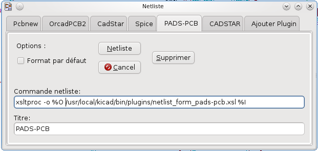
Configuration des paramètres du plugin
La configuration d’un plugin dans Eeschema requiert les informations suivantes :
-
Un titre : pour l’onglet, comme le nom du format de Netliste.
-
La ligne de commande pour lancer la conversion.
Quand vous cliquez sur le bouton netliste :
-
Eeschema crée un fichier netliste intermédiaire .xml, par exemple test.xml.
-
Eeschema lance le plugin, qui lit ce test.xml et crée la netliste test.net.
Génération de fichiers netlistes en ligne de commande
Partant du fait que nous utilisons le programme xsltproc.exe pour appliquer la feuille de style au fichier intermédiaire, xsltproc.exe sera exécuté avec la commande suivante :
xsltproc.exe -o <fichier de sortie> <fichier feuille de style> <fichier XML d’entrée à convertir>
Sous Windows, la ligne de commande sera la suivante :
f:/kicad/bin/xsltproc.exe -o "%O" f:/kicad/bin/plugins/netlist_form_pads-pcb.xsl "%I"
Sous Linux, la ligne de commande sera la suivante :
xsltproc -o "%O" /usr/local/kicad/bin/plugins/netlist_form_pads-pcb.xsl "%I"
Où netlist_form_pads-pcb.xsl est le nom de la feuille de style que vous voulez utiliser. N’oubliez pas les guillemets autour des noms de fichiers, ceci permet d’utiliser des espaces dans les noms des fichiers d’entrée et de sortie.
Le format de la ligne de commande accepte des paramètres de substitution pour les noms de fichiers :
Les paramètres autorisés sont.
-
%B ⇒ nom et chemin du fichier de sortie, sans le point et l’extension.
-
%I ⇒ nom et chemin complets du fichier d’entrée (le fichier intermédiaire de netliste).
-
%O ⇒ nom et chemin complets du fichier de sortie.
%I sera remplacé par le nom de fichier intermédiaire de netliste.
%O sera remplacé par le nom de fichier de sortie.
Format de ligne de commande : exemple pour xsltproc
Le format de ligne de commande de xsltproc est le suivant :
<chemin vers xsltproc> xsltproc <paramètres de xsltproc >
Sous Windows
f:/kicad/bin/xsltproc.exe -o "%O" f:/kicad/bin/plugins/netlist_form_pads-pcb.xsl "%I"
Sous Linux
xsltproc -o "%O" /usr/local/kicad/bin/plugins/netlist_form_pads-pcb.xsl "%I"
Les exemples ci-dessus supposent que xsltproc est installé sur votre PC sous Windows et que tous les fichiers sont situés dans F:\kicad\bin.
Génération de listes de composants (BOM)
Puisque le fichier netliste intermédiaire contient toutes les informations sur les composants utilisés, une liste de composants peut en être extraite. Voici la fenêtre de configuration du plugin (sous Linux) permettant de créer un fichier de BOM (Bill Of Materials) personnalisé :
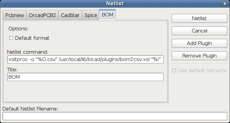
Le chemin vers la feuille de style bom2csv.xsl dépend de votre système. Actuellement, la meilleure feuille de style XSLT pour la génération du BOM est nommée bom2csv.xsl. Vous êtes libre de la modifier en fonction de vos besoins, et si vous développez un autre modèle utile à tous, vous pouvez demander qu’il fasse partie du projet KiCad.
Exemples de lignes de commandes pour les scripts Python
Le format d’une ligne de commande pour python ressemble à ceci :
python <fichier script> <fichier d’entrée> <fichier de sortie>
Sous Windows
python *.exe f:/kicad/python/my_python_script.py "%I" "%O"
Sous Linux
python /usr/local/kicad/python/my_python_script.py "%I" "%O"
Partant du fait que Python est effectivement installé sur votre PC..
Structure du fichier de netliste intermédiaire
L’exemple qui suit donne une idée du format du fichier de netliste intermédiaire.
<?xml version="1.0" encoding="utf-8"?>
<export version="D">
  <design>
    <source>F:\kicad_aux\netlist_test\netlist_test.sch</source>
    <date>29/08/2010 21:07:51</date>
    <tool>eeschema (2010-08-28 BZR 2458)-unstable</tool>
  </design>
  <components>
    <comp ref="P1">
      <value>CONN_4</value>
      <libsource lib="conn" part="CONN_4"/>
      <sheetpath names="/" tstamps="/"/>
      <tstamp>4C6E2141</tstamp>
    </comp>
    <comp ref="U2">
      <value>74LS74</value>
      <libsource lib="74xx" part="74LS74"/>
      <sheetpath names="/" tstamps="/"/>
      <tstamp>4C6E20BA</tstamp>
    </comp>
    <comp ref="U1">
      <value>74LS04</value>
      <libsource lib="74xx" part="74LS04"/>
      <sheetpath names="/" tstamps="/"/>
      <tstamp>4C6E20A6</tstamp>
    </comp>
    <comp ref="C1">
      <value>CP</value>
      <libsource lib="device" part="CP"/>
      <sheetpath names="/" tstamps="/"/>
      <tstamp>4C6E2094</tstamp>
    <comp ref="R1">
      <value>R</value>
      <libsource lib="device" part="R"/>
      <sheetpath names="/" tstamps="/"/>
      <tstamp>4C6E208A</tstamp>
    </comp>
  </components>
  <libparts/>
  <libraries/>
  <nets>
    <net code="1" name="GND">
      <node ref="U1" pin="7"/>
      <node ref="C1" pin="2"/>
      <node ref="U2" pin="7"/>
      <node ref="P1" pin="4"/>
    </net>
    <net code="2" name="VCC">
      <node ref="R1" pin="1"/>
      <node ref="U1" pin="14"/>
      <node ref="U2" pin="4"/>
      <node ref="U2" pin="1"/>
      <node ref="U2" pin="14"/>
      <node ref="P1" pin="1"/>
    </net>
    <net code="3" name="">
      <node ref="U2" pin="6"/>
    </net>
    <net code="4" name="">
      <node ref="U1" pin="2"/>
      <node ref="U2" pin="3"/>
    </net>
    <net code="5" name="/SIG_OUT">
      <node ref="P1" pin="2"/>
      <node ref="U2" pin="5"/>
      <node ref="U2" pin="2"/>
    </net>
    <net code="6" name="/CLOCK_IN">
      <node ref="R1" pin="2"/>
      <node ref="C1" pin="1"/>
      <node ref="U1" pin="1"/>
      <node ref="P1" pin="3"/>
    </net>
  </nets>
</export>
Structure générale
Le fichier de netliste intermédiaire contient cinq sections.
-
La section Entête.
-
The components section.
-
La section Composants en librairie.
-
La section Librairies.
-
La section Équipotentielles
Le contenu du fichier a pour balises de délimitations <export>
<export version="D">
...
</export>
Section Entête (Header)
L’entête a pour balises de délimitations <design>
<design>
<source>F:\kicad_aux\netlist_test\netlist_test.sch</source>
<date>21/08/2010 08:12:08</date>
<tool>eeschema (2010-08-09 BZR 2439)-unstable</tool>
</design>
Cette section peut être considérée comme une section de commentaires.
Section Composants
La section composants a pour balises de délimitations <components>
<components>
<comp ref="P1">
<value>CONN_4</value>
<libsource lib="conn" part="CONN_4"/>
<sheetpath names="/" tstamps="/"/>
<tstamp>4C6E2141</tstamp>
</comp>
</components>
Cette section contient la liste des composants de votre schéma. Chaque composant est décrit comme ceci :
<comp ref="P1">
<value>CONN_4</value>
<libsource lib="conn" part="CONN_4"/>
<sheetpath names="/" tstamps="/"/>
<tstamp>4C6E2141</tstamp>
</comp>
| libsource | name of the lib where this component was found. |
|---|---|
part |
component name inside this library. |
sheetpath |
path of the sheet inside the hierarchy: identify the sheet within the full schematic hierarchy. |
tstamps (time stamps) |
time stamp of the schematic file. |
tstamp (time stamp) |
time stamp of the component. |
Note à propos de l’horodatage des composants
Pour identifier un composant dans une netliste, et par voie de conséquence sur le circuit, l’horodatage est utilisé comme référence unique pour chaque composant. Toutefois, Kicad fournit un autre moyen pour identifier un composant, qui est son empreinte correspondante sur le circuit. Ceci permet la ré-annotation de composants dans un projet de schéma sans perdre le lien entre le composant et son empreinte.
Un horodatage (timestamp) est un identifiant unique pour chaque composant, ou chaque feuille d’un projet schématique. Cependant, dans des hiérarchies complexes, la même feuille étant utilisée plus d’une fois, cette feuille contiendra des composants avec le même horodatage.
Une feuille donnée à l’intérieur d’une hiérarchie complexe dispose d’un identifiant unique : son chemin de feuille (sheetpath). Un composant donné (à l’intérieur d’une hiérarchie complexe) a donc un identifiant unique : le sheetpath + son timestamp.
Section Composants en librairie (libparts)
La section libparts a pour délimiteur <libparts>, et le contenu de cette section est celui défini dans les librairies schématiques. La section libparts contient :
-
The allowed footprints names (names use wildcards) delimiter <fp>.
-
Les champs définis en librairie, avec pour délimiteur <fields>.
-
La liste des pins, avec pour délimiteur <pins>.
<libparts>
<libpart lib="device" part="CP">
  <description>Condensateur polarise</description>
  <footprints>
    <fp>CP*</fp>
    <fp>SM*</fp>
  </footprints>
  <fields>
    <field name="Reference">C</field>
    <field name="Valeur">CP</field>
  </fields>
  <pins>
    <pin num="1" name="1" type="passive"/>
    <pin num="2" name="2" type="passive"/>
  </pins>
</libpart>
</libparts>
Les lignes <pin num="1" type="passive"/> donnent aussi le type électrique de la pin. Les types électriques possibles sont :
Input |
Entrée |
Output |
Sortie |
Bidirectional |
Entrée ou Sortie |
Tri-state |
Trois-états |
Passive |
Extrémités de composants passifs |
Unspecified |
Non-Spécifié |
Power input |
Entrée d’alimentation d’un composant |
Power output |
Sortie d’alimentation, comme celle des régulateurs |
Open collector |
Collecteur ouvert |
Open emitter |
Émetteur ouvert |
Not connected |
Non-connecté, sera laissé en l’air dans le schéma |
Section Librairies
La section librairies a pour délimiteur <libraries>. Cette section contient la liste des librairies utilisées dans le projet.
<libraries>
  <library logical="device">
    <uri>F:\kicad\share\library\device.lib</uri>
  </library>
  <library logical="conn">
    <uri>F:\kicad\share\library\conn.lib</uri>
  </library>
</libraries>
Section Équipotentielles (nets)
La section nets a pour délimiteur <nets>. Cette section contient la liste des équipotentielles, la "connectivité" du schéma.
<nets>
  <net code="1" name="GND">
    <node ref="U1" pin="7"/>
    <node ref="C1" pin="2"/>
    <node ref="U2" pin="7"/>
    <node ref="P1" pin="4"/>
  </net>
  <net code="2" name="VCC">
    <node ref="R1" pin="1"/>
    <node ref="U1" pin="14"/>
    <node ref="U2" pin="4"/>
    <node ref="U2" pin="1"/>
    <node ref="U2" pin="14"/>
    <node ref="P1" pin="1"/>
  </net>
</nets>
Cette section recense toutes les équipotentielles du schéma.
Une entrée net peut contenir :
<net code="1" name="GND">
  <node ref="U1" pin="7"/>
  <node ref="C1" pin="2"/>
  <node ref="U2" pin="7"/>
  <node ref="P1" pin="4"/>
</net>
net code |
Identifiant interne pour ce net |
name |
Nom de ce net |
node |
Référence une pin de composant connectée à ce net |
Complément sur xsltproc
Réfère à la page : http://xmlsoft.org/XSLT/xsltproc.html
Introduction
xsltproc est un outil en ligne de commande pour appliquer des feuilles de styles XSLT à des documents XML. Bien qu’il ait été développé au sein du projet GNOME, il peut opérer indépendamment du bureau GNOME.
xsltproc est invoqué à partir de la ligne de commande, avec le nom de la feuille de style à utiliser, suivi du nom du ou des fichiers auxquels la feuille de style doit être appliquée. Il utilisera l’entrée standard si le nom de fichier d’entrée fournit est - .
Si une feuille de style est incluse dans un document XML, au moyen d’une instruction de traitement de feuille de style, il n’est pas nécessaire de spécifier la feuille de style sur la ligne de commande. xsltproc détectera automatiquement la feuille de style incluse et l’utilisera. Par défaut, la sortie est la sortie standard. Vous pouvez préciser un fichier de sortie en utilisant l’option -o.
Synoptique
xsltproc [[-V] | [-v] | [-o *file* ] | [--timing] | [--repeat] |
[--debug] | [--novalid] | [--noout] | [--maxdepth *val* ] | [--html] |
[--param *name* *value* ] | [--stringparam *name* *value* ] | [--nonet] |
[--path *paths* ] | [--load-trace] | [--catalogs] | [--xinclude] |
[--profile] | [--dumpextensions] | [--nowrite] | [--nomkdir] |
[--writesubtree] | [--nodtdattr]] [ *stylesheet* ] [ *file1* ] [ *file2* ]
[ *....* ]
Options de la ligne de commande
-V ou --version
Affiche les versions de libxml et libxslt qui sont utilisées.
-v ou --verbose
Affiche chaque étape de xsltproc lors du traitement du la feuille de style et du document.
-o ou --output fichier
Redirige la sortie vers le fichier nommé fichier. Pour des sorties multiples, que l’on appelle également ``chunking'', -o répertoire/ redirige les fichiers de sortie vers un répertoire donné. Le répertoire doit déjà exister.
--timing
Affiche le temps qu’il a fallu pour traiter la feuille de style, traiter le document, appliquer la feuille de style et enregistrer le résultat. Il est affiché en millisecondes.
--repeat
Lance la transformation 20 fois de suite. Utile pour des tests de vitesse.
--debug
Affiche un arbre XML du document transformé afin de déboguer.
--novalid
Évite le chargement de la DTD du document.
--noout
N’affiche pas le résultat.
--maxdepth valeur
Ajuste la profondeur maximale de la pile avant que libxslt ne conclue qu’il y ait une boucle infinie. La valeur par défaut est 500.
--html
Le document en entrée est un fichier HTML.
--param nom valeur
Passe un paramètre de nom nom et de valeur valeur à la feuille de style. Vous pouvez passer plusieurs paires nom/valeur, jusqu’à 32 valeurs. Si la valeur qui est spécifiée est une chaîne de caractères au lieu du nom d’identification d’un noeud, vous devez utiliser --stringparam à la place.
--stringparam nom valeur
Passe un paramètre de nom nom et de valeur valeur où valeur est une chaîne de caractères plutôt qu’un identifiant de noeud. (Note : La chaîne doit être en utf-8.)
--nonet
Ne pas utiliser Internet pour récupérer les DTD ou les entités.
--path chemins
Use the list (separated by space or column) of filesystem paths specified by paths to load DTDs, entities or documents.
--load-trace
Affiche sur la sortie d’erreurs standard (stderr) tous les documents chargés pendant le traitement.
--catalogs
Utilise les catalogues SGML pour résoudre l’emplacement des entités externes. Par défaut xsltproc utilise les catalogues XML installés dans /etc/xml/catalog.
--xinclude
Traite le document en entrée en utilisant les spécifications Xinclude. Vous pouvez obtenir plus de détails dans les spécifications de Xinclude : http://www.w3.org/TR/xinclude/.
--profile --norman
Donne des informations détaillant le temps passé pour chaque partie de la feuille de style. C’est utile pour optimiser les performances de la feuille de style.
--dumpextensions
Affiche la liste de toutes les extensions enregistrées sur la sortie standard (stdout).
--nowrite
N’écrit sur aucun fichier ni ressource.
--nomkdir
Ne crée aucun répertoire.
--writesubtree chemin
Autorise l’écriture de fichiers seulement sur le sous-répertoire chemin.
--nodtdattr
N’applique pas les attributs par défaut de la DTD du document.
Valeurs de retour de xsltproc
xsltproc renvoie un code fournissant des informations qui peuvent être très utiles lorsqu’on l’utilise dans des scripts.
0 : normal
1 : pas d’argument
2 : trop de paramètres
3 : option inconnue
4 : le traitement de la feuille de style a échoué
5 : erreur dans la feuille de style
6 : erreur dans un des documents
7 : méthode de sortie xsl (xsl:output) non-supportée
8 : la chaîne de paramètres contient à la fois des guillemets simples et doubles
9 : erreur interne de traitement
10 : le traitement a été stoppé par un signal d’achèvement
11: Impossible d’écrire le résultat dans le fichier de sortie
Plus d’infos sur xsltproc
Page web de la libxml : http://www.xmlsoft.org/
Page XSLT sur le W3C : http://www.w3.org/TR/xslt
Simulator
Eeschema provides an embedded electrical circuit simulator using ngspice as the simulation engine.
When working with the simulator, you may find the official pspice library useful. It contains common symbols used for simulation like voltage/current sources or transistors with pins numbered to match the ngspice node order specification.
There are also a few demo projects to illustrate the simulator capabilities. You will find them in demos/simulation directory.
Assigning models
Before a simulation is launched, components need to have Spice model assigned.
Each component can have only one model assigned, even if component consists of multiple units. In such case, the first unit should have the model specified.
Passive components with reference matching a device type in Spice notation (R* for resistors, C* for capacitors, L* for inductors) will have models assigned implicitly and use the value field to determine their properties.
| Keep in mind that in Spice notation 'M' stands for milli and 'Meg' corresponds to mega. If you prefer to use 'M' to indicate mega prefix, you may request doing so in the simulation settings dialog. |
Spice model information is stored as text in symbol fields, therefore you may either define it in symbol editor or schematics editor. Open symbol properties dialog and click on Edit Spice Model button to open Spice Model Editor dialog.
Spice Model Editor dialog has three tabs corresponding to different model types. There are two options common to all model types:
Disable symbol for simulation |
When checked the component is excluded from simulation. |
Alternate node sequence |
Allows one to override symbol pin to model node mapping. To define a different mapping, specify pin numbers in order expected by the model. 'Example:'
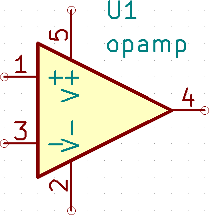
To match the symbol pins to the Spice model nodes shown above, one needs to use an alternate node sequence option with value: "1 3 5 2 4". It is a list of pin numbers corresponding to the Spice model nodes order. |
Passive
Passive tab allows the user to assign a passive device model (resistor, capacitor or inductor) to a component. It is a rarely used option, as normally passive components have models assigned implicitly, unless component reference does not match the actual device type.
| Explicitly defined passive device models have priority over the ones assigned implicitly. It means that once a passive device model is assigned, the reference and value fields are not taken into account during simulation. It may lead to a confusing situation when assigned model value does not match the one displayed on a schematic sheet. |
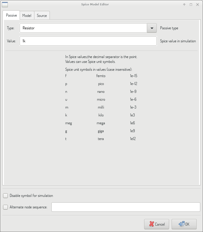
Type |
Selects the device type (resistor, capacitor or inductor). |
Value |
Defines the device property (resistance, capacitance or inductance). The value may use common Spice unit prefixes (as listed below the text input field) and should use point as the decimal separator. Note that Spice does not correctly interpret prefixes intertwined in the value (e.g. 1k5). |
Model
Model tab is used to assign a semiconductor or a complex model defined in an external library file. Spice model libraries are often offered by device manufacturers.
The main text widget displays the selected library file contents. It is a common practice to put models description inside library files, including the node order.
File |
Path to a Spice library file. This file is going to be used by the simulator, as it is added using .include directive. |
Model |
Selected device model. When a file is selected, the list is filled with available models to choose from. |
Type |
Selects model type (subcircuit, BJT, MOSFET or diode). Normally it is set automatically when a model is selected. |
Source
Source tab is used to assign a power or signal source model. There are two sections: DC/AC analysis and Transient analysis. Each defines source parameters for the corresponding simulation type.
Source type option applies to all simulation types.
Refer to the ngspice documentation, chapter 4 (Voltage and Current Sources) for more details about sources.
Spice directives
It is possible to add Spice directives by placing them in text fields on a schematic sheet. This approach is convenient for defining the default simulation type. This functionality is limited to Spice directives starting with a dot (e.g. ".tran 10n 1m"), it is not possible to place additional components using text fields.
Simulation
To launch a simulation, open Spice Simulator dialog by selecting menu Tools→Simulator in the schematics editor window.
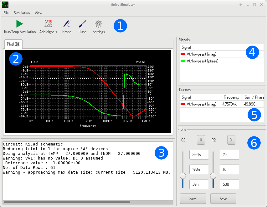
The dialog is divided into several sections:
Menu
File
New Plot |
Create a new tab in the plot panel. |
Open Workbook |
Open a list of plotted signals. |
Save Workbook |
Save a list of plotted signals. |
Save as image |
Export the active plot to a .png file. |
Save as .csv file |
Export the active plot raw data points to a .csv file. |
Exit Simulation |
Close the dialog. |
Simulation
Run Simulation |
Perform a simulation using the current settings. |
Add signals… |
Open a dialog to select signals to be plotted. |
Probe from schematics |
Start the schematics Probe tool. |
Tune component value |
Start the Tuner tool. |
Show SPICE Netlist… |
Open a dialog showing the generated netlist for the simulated circuit. |
Settings… |
Open the simulation settings dialog. |
View
Zoom In |
Zoom in the active plot. |
Zoom Out |
Zoom out the active plot. |
Fit on Screen |
Adjust the zoom setting to display all plots. |
Show grid |
Toggle grid visibility. |
Show legend |
Toggle plot legend visibility. |
Toolbar
The top toolbar provides access to the most frequently performed actions.
Run/Stop Simulation |
Start or stop the simulation. |
Add Signals |
Open a dialog to select signals to be plotted. |
Probe |
Start the schematics Probe tool. |
Tune |
Start the Tuner tool. |
Settings |
Open the simulation settings dialog. |
Plot panel
Visualizes the simulation results as plots. One can have multiple plots opened in separate tabs, but only the active one is updated when a simulation is executed. This way it is possible to compare simulation results for different runs.
Plots might be customized by toggling grid and legend visibility using View menu. When a legend is visible, it can be dragged to change its position.
Plot panel interaction:
-
scroll mouse wheel to zoom in/out
-
right click to open a context menu to adjust the view
-
draw a selection rectangle to zoom in the selected area
-
drag a cursor to change its coordinates
Output console
Output console displays messages from the simulator. It is advised to check the console output to verify there are no errors or warnings.
Signals list
Shows the list of signals displayed in the active plot.
Signals list interaction:
-
right click to open a context menu to hide signal or toggle cursor
-
double click to hide signal
Cursors list
Shows the list of cursors and their coordinates. Each signal may have one cursor displayed. Cursors visibility is set using the Signals list.
Tune panel
Displays components picked with the Tuner tool. Tune panel allows the user to quickly modify component values and observe their influence on the simulation results - every time a component value is changed, the simulation is rerun and plots are updated.
For each component there a few controls associated:
-
The top text field sets the maximum component value.
-
The middle text field sets the actual component value.
-
The bottom text field sets the minimum component value.
-
Slider allows the user to modify the component value in a smooth way.
-
Save button modifies component value on the schematics to the one selected with the slider.
-
X button removes component from the Tune panel and restores its original value.
The three text fields recognize Spice unit prefixes.
Tuner tool
Tuner tool lets the user pick components for tuning.
To select a component for tuning, click on one in the schematics editor when the tool is active. Selected components will appear in the Tune panel. Only passive components might be tuned.
Probe tool
Probe tool provides an user-friendly way of selecting signals for plotting.
To add a signal to plot, click on a corresponding wire in the schematics editor when the tool is active.
Simulation settings
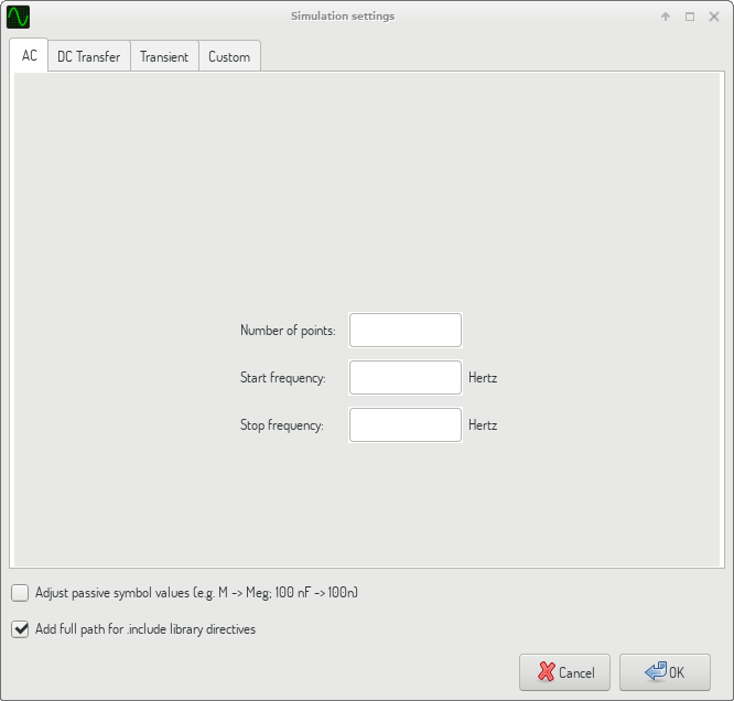
Simulation settings dialog lets the user set the simulation type and parameters. There are four tabs:
-
AC
-
DC Transfer
-
Transient
-
Custom
The first three tabs provide forms where simulation parameters might be specified. The last tab allows the user to type in custom Spice directives to set up a simulation. You can find more information about simulation types and parameters in the ngspice documentation, chapter 1.2.
An alternative way to configure a simulation is to type Spice directives into text fields on schematics. Any text field directives related to simulation type are overridden by the settings selected in the dialog. It means that once you start using the simulation dialog, the dialog overriddes the schematics directives until the simulator is reopened.
There are two options common to all simulation types:
Adjust passive symbol values |
Replace passive symbol values to convert common component values notation to Spice notation. |
Add full path for .include library directives |
Prepend Spice model library file names with full path. Normally full path is required by ngspice to access a library file. |