Podręcznik użytkownika
| This manual is in the process of being revised to cover the latest stable release version of KiCad. It contains some sections that have not yet been completed. We ask for your patience while our volunteer technical writers work on this task, and we welcome new contributors who would like to help make KiCad’s documentation better than ever. |
Prawa autorskie
This document is Copyright © 2010-2022 by its contributors as listed below. You may distribute it and/or modify it under the terms of either the GNU General Public License (http://www.gnu.org/licenses/gpl.html), version 3 or later, or the Creative Commons Attribution License (http://creativecommons.org/licenses/by/3.0/), version 3.0 or later.
Wszystkie znaki towarowe użyte w tym dokumencie należą do ich właścicieli.
Współtwórcy
Jean-Pierre Charras, Fabrizio Tappero, Wayne Stambaugh, Graham Keeth
Tłumaczenie
Kerusey Karyu <[email protected]>, 2014-2015.
Kontakt
The KiCad project welcomes feedback, bug reports, and suggestions related to the software or its documentation. For more information on how to sumbit feedback or report an issue, please see the instructions at https://www.kicad.org/help/report-an-issue/
Introduction to the KiCad Schematic Editor
Opis
The KiCad Schematic Editor is a schematic capture software distributed as a part of KiCad and available under the following operating systems:
-
Linux
-
Apple macOS
-
Windows
Regardless of the OS, all KiCad files are 100% compatible from one OS to another.
The Schematic Editor is an integrated application where all functions of drawing, control, layout, library management and access to the PCB design software are carried out within the editor itself.
The KiCad Schematic Editor is intended to cooperate with the KiCad PCB Editor, which is KiCad’s printed circuit design software. It can also export netlist files, which lists all the electrical connections, for other packages.
The Schematic Editor includes a symbol library editor, which can create and edit symbols and manage libraries. It also integrates the following additional but essential functions needed for modern schematic capture software:
-
Sprawdzanie poprawności projektu (DRC) dla zautomatyzowanego procesu kontroli poprawności połączeń, czy testowania niepołączonych wejść elementów.
-
Generowanie wydruków w różnych formatach (Postscript, PDF, HPGL oraz SVG).
-
Tworzenie list materiałowych (za pomocą skryptów Python lub XSLT, które pozwalają na różnorodną jej konfigurację).
The Schematic Editor supports multi-sheet schematics in several ways:
-
Flat hierarchies (schematic sheets are not explicitly connected in a master diagram).
-
Simple hierarchies (each schematic sheet is used only once).
-
Complex hierarchies (some schematic sheets are used multiple times).
Hierarchical schematics are described in detail later in the manual.
Konfiguracja początkowa
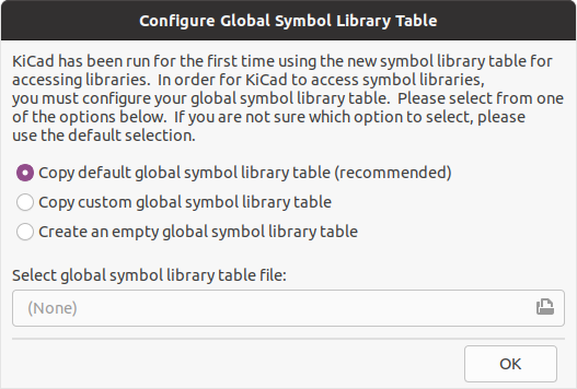
When the Schematic Editor is run for the first time, if the the global symbol library table file sym-lib-table is not found in the KiCad configuration folder then KiCad will ask how to create this file:
The first option is recommended (Copy default global symbol library table (recommended)). The default symbol library table includes all of the standard symbol libraries that are installed as part of KiCad.
If this option is disabled, KiCad was unable to find the default global symbol library table. This probably means you did not install the standard symbol libraries with KiCad, or they are not installed where KiCad expects to find them. On some systems the KiCad libraries are installed as a separate package.
-
If you have installed the standard KiCad symbol libraries and want to use them, but the first option is disabled, select the second option and browse to the
sym-lib-tablefile in the directory where the KiCad libraries were installed. -
If you already have a custom symbol library table that you would like to use, select the second option and browse to your
sym-lib-tablefile. -
If you want to construct a new symbol library table from scratch, select the third option.
Symbol library management is described in more detail later.
The Schematic Editor User Interface
The main Schematic Editor user interface is shown above. The center contains the main editing canvas, which is surrounded by:
-
Top toolbars (file management, zoom tools, editing tools)
-
Left toolbar (display options)
-
Message panel and status bar at bottom
-
Right panel (drawing and design tools)
Navigating the editing canvas
The editing canvas displays the schematic being designed. You can pan and zoom to different parts of the schematic and open any schematic sheet in the design.
By default, dragging with the middle or right mouse button will pan the canvas view and scrolling the mouse wheel will zoom the view in or out. You can change this behavior in the Mouse and Touchpad section of the preferences (see Configuration and Customization for details).
Several other zoom tools are available in the top toolbar:
-
 zooms in on the center of the viewport.
 -
 zooms out from the center of the viewport.
 -
 zooms to fit the frame around the drawing sheet.
 -
 zooms to fit the items within the drawing sheet.
 -
 allows you to draw a box to determine the zoomed area.
The cursor’s current position is displayed at the bottom of the window (X and Y), along with the current zoom factor (Z), the cursor’s relative position (dx, dy, and dist), the grid setting, and the display units.
The relative coordinates can be reset to zero by pressing Space. This is useful for measuring distance between two points or aligning objects.
Klawisze skrótów
The Ctrl+F1 shortcut displays the current hotkey list. The default hotkey list is included in the Actions Reference section of the manual.
The hotkeys described in this manual use the key labels that appear on a standard PC keyboard. On an Apple keyboard layout, use the Cmd key in place of Ctrl, and the Option key in place of Alt.
Many actions do not have hotkeys assigned by default, but hotkeys can be assigned or redefined using the hotkey editor (Preferences → Preferences… → Hotkeys).
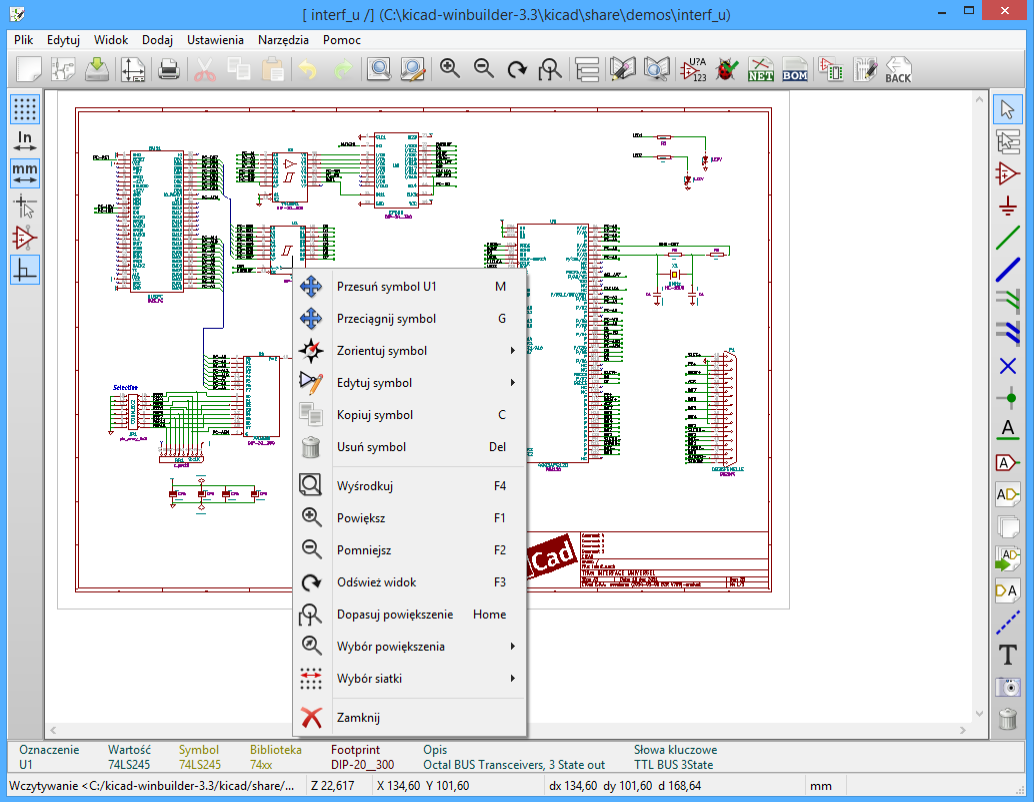
| Many of the actions available through hotkeys are also available in context menus. To access the context menu, right-click in the editing canvas. Different actions will be available depending on what is selected or what tool is active. |
Hotkeys are stored in the file user.hotkeys in KiCad’s configuration directory. The location is platform-specific:
-
Windows:
%APPDATA%\kicad\6.0\user.hotkeys -
Linux:
~/.config/kicad/6.0/user.hotkeys -
macOS:
~/Library/Preferences/kicad/6.0/user.hotkeys
KiCad can import hotkey settings from a user.hotkeys file using the Import Hotkeys button in the hotkey editor.
Mouse operations and selection
Selecting items in the editing canvas is done with the left mouse button. Single-clicking on an object will select it and dragging will perform a box selection. A box selection from left to right will only select items that are fully inside the box. A box selection from right to left will select any items that touch the box. A left-to-right selection box is drawn in yellow, with a cursor that indicates exclusive selection, and a right-to-left selection box is drawn in blue with a cursor that indicates inclusive selection.
The selection action can be modified by holding modifier keys while clicking or dragging. The following modifier keys apply when clicking to select single items:
| Modifier Keys (Windows) | Modifier Keys (Linux) | Modifier Keys (macOS) | Selection Effect |
|---|---|---|---|
Shift |
Shift |
Shift |
Add the item to the existing selection. |
Ctrl+Shift |
Ctrl+Shift |
Cmd+Shift |
Remove the item from the existing selection. |
long click |
long click or Alt |
long click or Option |
Clarify selection from a pop-up menu. |
Ctrl |
Ctrl |
Cmd |
Highlight the net of the selected copper item. |
The following modifier keys apply when dragging to perform a box selection:
| Modifier Keys (Windows) | Modifier Keys (Linux) | Modifier Keys (macOS) | Selection Effect |
|---|---|---|---|
Shift or Ctrl |
Shift or Ctrl |
Shift or Ctrl |
Add item(s) to the existing selection. |
Ctrl+Shift |
Ctrl+Shift |
Cmd+Shift |
Remove item(s) from the existing selection. |
Selecting an object displays information about the object in the message panel at the bottom of the window. Double-clicking an object opens a window to edit the object’s properties.
Pressing Esc will always cancel the current tool or operation and return to the selection tool. Pressing Esc while the selection tool is active will clear the current selection.
Left toolbar display controls
The left toolbar provides options to change the display of items in the Schematic Editor.
|
Turns grid display on/off. Note: by default, hiding the grid will disable grid snapping. This behavior can be changed in the Display Options section of Preferences. |
|
Display/entry of coordinates and dimensions in inches, mils, or millimeters. |
|
Switches between full-screen and small editing cursor (crosshairs). |
|
Turns invisible pin display on/off. |
|
Switches between free angle and horizontal/vertical placement of new wires, buses, and graphical lines. |
Tworzenie i edycja schematu
Wprowadzenie
A schematic designed with KiCad is more than a simple graphic representation of an electronic device. It is normally the entry point of a development chain that allows for:
-
Walidację za pomocą zbioru reguł (ERC) by wykryć proste błędy oraz braki na schemacie.
-
Automatically generating a bill of materials.
-
Generowanie listy sieci dla oprogramowania do symulacji, takiego jak Spice.
-
Defining a circuit for transferring to PCB layout.
Schemat składa się głównie z elementów, połączeń między nimi, etykiet, węzłów, magistral i portów zasilania. Dla zwiększenia czytelności schematu, można umieścić elementy graficzne takie jak: wejścia do magistral, komentarze i linie przerywane do budowy ramek.
Symbols are added to the schematic from symbol libraries. After the schematic is made, the set of connections and footprints is imported into the PCB editor for designing a board.
Schematics can be contained in a single sheet or split among multiple sheets. In KiCad, multi-sheet schematics are organized hierarchically, with a root sheet and sub-sheet(s). Each sheet is its own .kicad_sch file and is itself a complete KiCad schematic. Working with hierarchical schematics is described in the Hierarchical Schematics chapter.
Schematic editing operations
Schematic editing tools are located in the right toolbar. When a tool is activated, it stays active until a different tool is selected or the tool is canceled with the Esc key. The selection tool is always activated when any other tool is canceled.
|
Selection tool (the default tool) |
|
Highlight a net by marking its wires and net labels with a different color. If the PCB Editor is also open then copper corresponding to the selected net will be highlighted as well. Net highlighting can be cleared by clicking with the highlight tool in an empty space, or by using the Clear Net Highlighting hotkey (~). |
|
Display the symbol selector dialog to place a new symbol. |
|
Display the power symbol selector dialog to place a new power symbol. |
|
Draw a wire. |
|
Draw a bus. |
|
Draw wire-to-bus entry points. These elements are only graphical and do not create a connection, thus they should not be used to connect wires together. |
|
Place a "No Connect" flag. These flags should be placed on symbol pins which are meant to be left unconnected. "No connect" flags indicate to the Electrical Rule Checker that the pin is intentionally unconnected and not an error. |
|
Place a junction. This connects two crossing wires or a wire and a pin, which can sometimes be ambiguous without a junction (i.e. if a wire end or a pin is not directly connected to another wire end). |
|
Place a local label. Local labels connect items located in the same sheet. For connections between two different sheets, use global or hierarchical labels. |
|
Place a global label. All global labels with the same name are connected, even when located on different sheets. |
|
Place a hierarchical label. Hierarchical labels are used to create a connection between a subsheet and the sheet’s parent sheet. See the Hierarchical Schematics section for more information about hierarchical labels, sheets, and pins. |
|
Place a hierarchical subsheet. You must specify the file name for this subsheet. |
|
Import a hierarchical pin from a subsheet. This command can be executed only on hierarchical subsheets. It will create hierarchical pins corresponding to hierarchical labels placed in the target subsheet. |
|
Draw lines. Note: Lines are graphical objects and are not the same as wires placed with the Wire tool. They do not connect anything. |
|
Place a text comment. |
|
Place a bitmap image. |
|
Delete clicked items. |
Grids
In the Schematic Editor the cursor always moves over a grid. The grid can be customized:
-
Size can be changed using the right click menu or using View → Grid Properties….
-
Color can be changed in the Colors page of the Preferences dialog (menu Preferences → General Options).
-
Visibility can be switched using the left-hand toolbar button.
The default grid size is 50 mil (0.050") or 1.27 millimeters.
This is the recommended grid for placing symbols and wires in a schematic, and for placing pins when designing a symbol in the Symbol Editor.
| Wires connect with other wires or pins only if their ends coincide exactly. Therefore it is very important to keep symbol pins and wires aligned to the grid. It is recommended to always use a 50 mil grid when placing symbols and drawing wires because the KiCad standard symbol library and all libraries that follow its style also use a 50 mil grid. Using a grid size other than 50 mil will result in schematics without proper connectivity! |
Smaller grids can also be used, but this is intended only for text and symbol graphics, and not recommended for placing pins and wires.
| Symbols, wires, and other elements that are not aligned to the grid can be snapped back to the grid by selecting them, right clicking, and clicking Align Elements to Grid. |
Snapping
Schematic elements such as symbols, wires, text, and graphic lines are snapped to the grid when moving, dragging, and drawing them. Additionally, the wire tool snaps to pins even when grid snapping is disabled. Both grid and pin snapping can be disabled while moving the mouse by using the modifier keys in the table below.
| On Apple keyboards, use the Cmd key instead of Ctrl. |
| Modifier Key | Effect |
|---|---|
Ctrl |
Disable grid snapping. |
Shift |
Disable snapping wires to pins. |
Working with symbols
Placing symbols
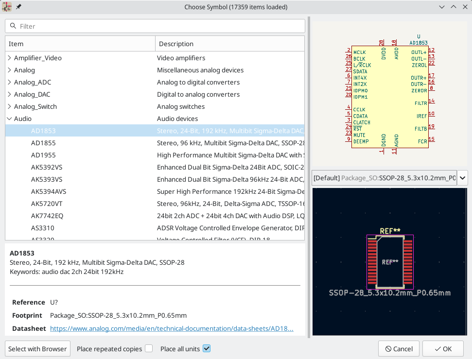
To load a symbol into your schematic you can use the icon ![]() . A dialog box allows you to type the name of the symbol to load.
. A dialog box allows you to type the name of the symbol to load.
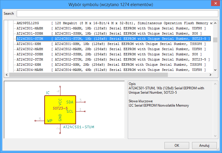
The Choose Symbols dialog will filter symbols by name, keywords, and description according to what you type into the search field.
Some advanced filters are available:
-
Wildcards: use the characters
?and*respectively to mean "any single character or no characters" and "any number of any characters, including none". -
Key-value pairs: if a library part’s description or keywords contain a tag of the format "Key:123", you can match relative to that by typing "Key>123" (greater than), "Key<123" (less than), etc. Numbers may include one of the following case-insensitive suffixes:
p
n
u
m
k
meg
g
t
10-12
10-9
10-6
10-3
103
106
109
1012
ki
mi
gi
ti
210
220
230
240
-
Regular expressions: if you’re familiar with regular expressions, these can be used too. The regular expression flavor used is the wxWidgets Advanced Regular Expression style, which is similar to Perl regular expressions.
If the symbol specifies a default footprint, this footprint will be previewed in the lower right. If the symbol includes footprint filters, alternate footprints that satisfy the footprint filters can be selected in the footprint dropdown menu at right.
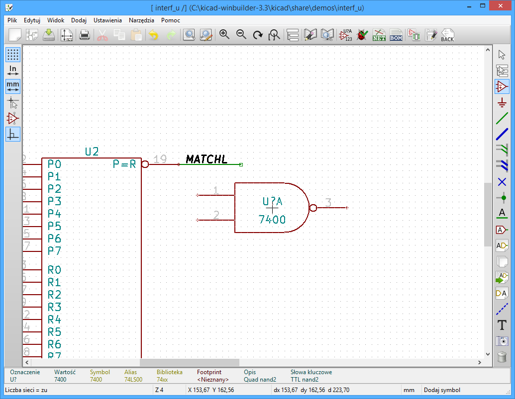
After selecting a symbol to place, the symbol will be attached to the cursor. Left clicking the desired location in the schematic places the symbol into the schematic. Before placing the symbol in the schematic, you can rotate it, mirror it, and edit its fields, by either using the hotkeys or the right-click context menu. These actions can also be performed after placement.
Poniższy obrazek pokazuje symbol podczas operacji wstawiania go do schematu:
If the Place repeated copies option is checked, after placing a symbol KiCad will start placing another copy of the symbol. This process continues until the user presses Esc.
For symbols with multiple units, if the Place all units option is checked, after placing the symbol KiCad will start placing the next unit in the symbol. This continues until the last unit has been placed or the user presses Esc.
Placing power ports
A power port symbol is a symbol representing a connection to a power net. The symbols are grouped in the power library, so they can be placed using the symbol chooser. However, as power placements are frequent, the ![]() tool is available. This tool is similar, except that the search is done directly in the
tool is available. This tool is similar, except that the search is done directly in the power library and any other library that contains power symbols.
Moving symbols
Symbols can be moved using the Move (M) or Drag (G) tools. These tools act on the selected symbol, or if no symbol is selected they act on the symbol under the cursor.
The Move tool moves the symbol itself without maintaining wired connections to the symbol pins.
The Drag tool moves the symbol without breaking wired connections to its pins, and therefore moves the connected wires as well.
You can also Drag symbols by clicking and dragging them with the mouse, depending on the Left button drag gesture setting in the Mouse and Touchpad section of Preferences.
Symbols can also be rotated (R) or mirrored in the X (X) or Y (Y) directions.
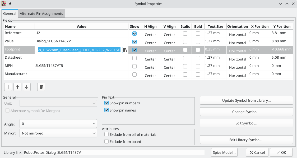
Editing symbol properties
A symbol’s fields can be edited in the symbol’s Properties window. Open the Symbol Properties window for a symbol with the E hotkey or by double-clicking on the symbol.
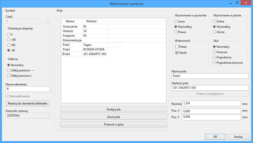
The Symbol Properties window displays all the fields of a symbol in a table. New fields can be added, and existing fields can be deleted, edited, reordered, moved, or resized.
Każde pole może być widoczne lub nie oraz wyświetlane poziomo lub pionowo. Wyświetlana pozycja jest zawsze pokazywana dla normalnie wyświetlanego elementu (bez obrotu lub lustra) i odnosi się do punktu aktywnego elementu.
The position and orientation properties of each field may be hidden in this dialog. They can be shown by right-clicking on the column header of the fields table and enabling the "Orientation", "X Position", and/or "Y Position" columns. Other columns can be shown or hidden as desired.
The "Update Symbol from Library…" button is used to update the schematic’s copy of the symbol to match the copy in the library. The "Change Symbol…" button is used to swap the current symbol to a different symbol in the library.
"Edit Symbol…" opens the Symbol Editor to edit the copy of the symbol in the schematic. Note that the original symbol in the library will not be modified. The "Edit Library Symbol…" button opens the Symbol Editor to edit the original symbol in the library. In this case, the symbol in the schematic will not be modified until the user clicks the "Update Symbol from Library…" button.
Editing symbol fields individually
An individual symbol text field can be edited directly with the E hotkey (with a field selected instead of a symbol) or by double-clicking on the field.
Some symbol fields have their own hotkey to edit them directly. With the symbol selected, the Reference, Value, and Footprint fields can be edited with the U, V, or F hotkeys, respectively.
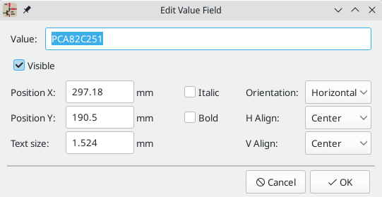
The options in this dialog are the same as those in the full Symbol Properties dialog, but are specific to a single field.
Symbol fields can be automatically moved to an appropriate location with the Autoplace Fields action (select a symbol and press O). Field autoplacement is configurable in the Schematic Editor’s Editing Options, including a setting to always autoplace fields.
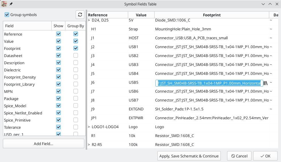
Symbol Fields Table
The Symbol Fields Table allows you to view and modify field values for all symbols in a spreadsheet interface. You can open the Symbol Fields Table with the ![]() button.
button.
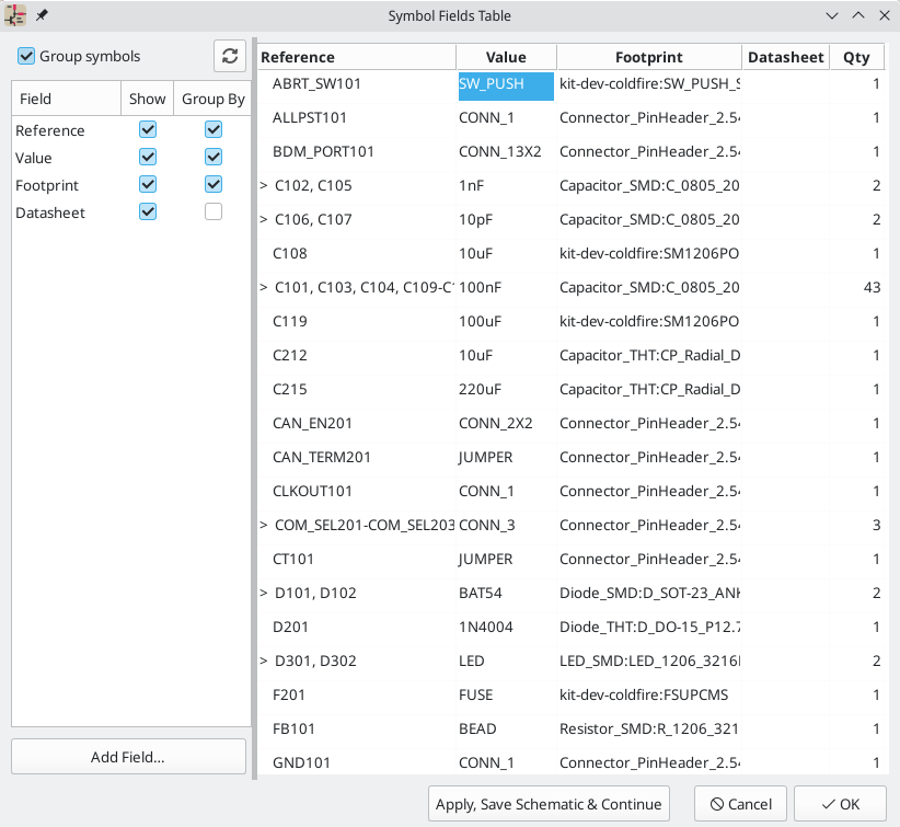
Cells are navigated with the arrow keys, or with Tab / Shift+Tab to move right / left and Enter / Shift+Enter to move down / up, respectively.
A range of cells can be selected by clicking and dragging. The whole range of selected cells will be copied (Ctrl+C) or pasted into (Ctrl+V) on a copy or paste action. Copying a range of cells from the table can be useful for creating a BOM. More details of copying and pasting cells are described below.
Any symbol field can be shown or hidden using the Show checkboxes on the left, or by right-clicking on the header of the table. New symbol fields can be added using the Add Field… button.
Similar symbols can optionally be grouped by any symbol field using the Group By checkboxes. Grouped symbols are shown in a single row in the table. The grouped row can be expanded to show the individual symbols by clicking the arrow at the left of the row.
Tricks to simplify filling fields
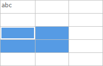
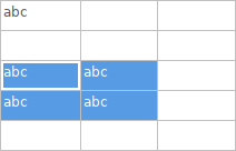
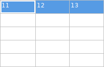
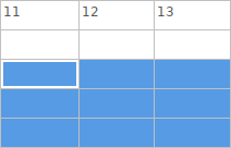
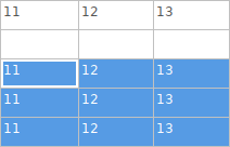
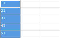
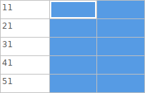
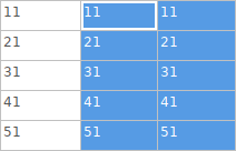
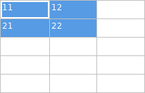
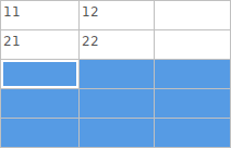
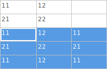
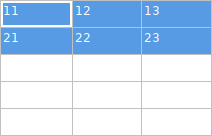
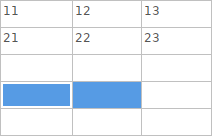
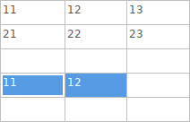
There are several special copy/paste methods in the spreadsheet for pasting values into larger regions, including auto-incrementing pasted cells. These features may be useful when pasting values that are shared in several symbols.
These methods are illustrated below.
| 1. Copy (Ctrl+C) | 2. Select target cells | 3. Paste (Ctrl+V) |
|---|---|---|
|
|
|
|
|
|
|
|
|
|
|
|
|
|
|
| Te techniki są również dostępne w innych oknach dialogowych zawierających tabele. |
Reference Designators and Symbol Annotation
Reference designators are unique identifiers for components in a design. They are often printed on a PCB and in assembly diagrams, and allow you to match symbols in a schematic to the corresponding components on a board.
In KiCad, reference designators consist of a letter indicating the type of component (R for resistor, C for capacitor, U for IC, etc.) followed by a number. If the symbol has multiple units then the reference designator will also have a trailing letter indicating the unit. Symbols that don’t have a reference designator set have a ? character instead of the number. Reference designators must be unique.
Reference designators can set manually by editing a symbol’s reference designator field, or automatically using the Annotation tool.
| The process of setting a symbol’s reference designator is called annotation. |
Numeracja komponentów
The Annotation tool automatically assigns reference designators to symbols in the schematic. To launch the Annotation tool, click the ![]() button in the top toolbar.
button in the top toolbar.
The tool provides several options to control how symbols are annotated.
Scope: Selects whether annotation is applied to the entire schematic, to only the current sheet, or to only the selected symbols.
Options: Selects whether annotation should apply to all symbols and reset *existing reference designators, or apply only to unannotated symbols.
Order: Chooses the direction of numbering. If symbols are sorted by X position, all symbols on the left side of a schematic sheet will be lower numbered than symbols on the right side of the sheet. If symbols are sorted by Y position, all symbols on the top of a sheet will be lower numbered than symbols at the bottom of the sheet.
Numbering: Selects the starting point for numbering reference designators. The lowest unused number above the starting point is picked for each reference designator. The starting point can be an arbitrary number (typically zero), or it can be the sheet number multiplied by 100 or 1000 so that each part’s reference designator corresponds to the schematic page it is on.
The Clear Annotation button clears all reference designators in the selected scope.
Annotation messages can be filtered with the checkboxes at the bottom or saved to a report using the Save… button.
Electrical Connections
There are two primary ways to establish connections: wires and labels. Both are shown in the schematic below.
Connections can also be made with buses and with implicit connections via hidden power pins.
This section will also discuss two special types of symbols that can be added with the "Power port" button on the right toolbar:
-
Power ports: symbols for connecting wires to a power or ground net.
-
PWR_FLAG: a specific symbol for indicating that a net is powered when it is not connected to a power output pin (for example, a power net that is supplied by an off-board connector).
Label Connections
Labels are used to assign net names to wires and pins. Wires with the same net name are considered to be connected. A net can only have one name. If two different labels are placed on the same net, an ERC violation will be generated. Only one of the net names will be used in the netlist. The final net name is determined according to the rules described below.
There are three types of labels, each with a different connection scope.
-
Local labels, also referred to simply as labels, only make connections within a sheet. Add a local label with the
 button in the right
toolbar.
button in the right
toolbar. -
Global labels make connections anywhere in a schematic, regardless of sheet. Add a global label with the
 button in the right
toolbar.
button in the right
toolbar. -
Hierarchical labels connect to hierarchical sheet pins and are used in hierarchical schematics for connecting child sheets to their parent sheet. Add a hierarchical label with the
 button in the right toolbar.
| Labels that have the same name will connect, regardless of the label type, if they are in the same sheet. |
After using the appropriate button or hotkey to create a label, the Label Properties dialog appears.
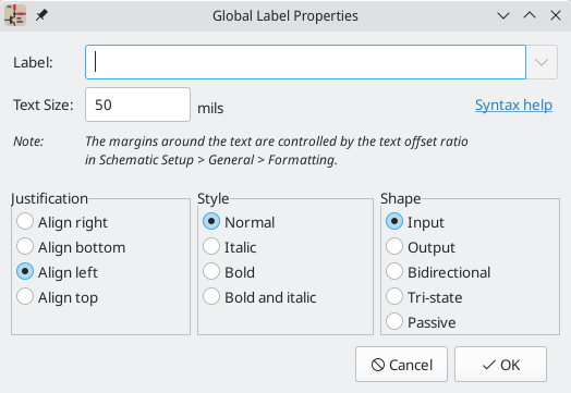
The Label field sets the label’s text, which determines the net that the label assigns to its attached wire. Label text supports markup for overbars, subscripts, etc., as well as variable substitution. Use the Syntax help link in the dialog for a summary.
Justification sets the position of the label’s connection point relative to the label’s text. For example, when Align right is selected the connection point will be to the right of the text.
Text size and Style control the appearance of the label’s text. Shape controls the shape of the outline around the label; this is purely visual and has no electrical consequence. Local labels do not have an outline, and therefore do not have Shape options.
| Global labels have additional settings to control margins around the label text in the Schematic Setup dialog. |
After accepting the label properties, the label is attached to the cursor for placement. The connection point for a label is the small square in the corner of the label. The square disappears when the label is connected to a wire or the end of a pin.

The connection point’s position relative to the label text can be changed by choosing a different label orientation in the label’s properties, or by mirroring/rotating the label.
The Label Properties dialog can be accessed at any time by selecting a label and using the E hotkey, double-clicking on the label, or with Properties… in the right-click context menu.
Wire Connections
To establish a connection, a segment of wire must be connected by its end to another segment or to a pin. Only wire ends create connections; if a wire crosses the middle of another wire, a connection will not be made.
Unconnected wire ends have a small square that indicates the connection point. The square disappears when a connection is made to the wire end. Unconnected pins have a circle, which also disappears when a connection is made.
| Wires connect with other wires or pins only if their ends coincide exactly. Therefore it is important to keep symbol pins and wires aligned to the grid. It is recommended to always use a 50 mil grid when placing symbols and drawing wires because the KiCad standard symbol library and all libraries that follow its style also use a 50 mil grid. |
| Symbols, wires, and other elements that are not aligned to the grid can be snapped back to the grid by selecting them, right clicking, and selecting Align Elements to Grid. |
Drawing and editing wires
To begin connecting elements with wire, use the Wire tool ![]() in the right toolbar (w). Wires can also be automatically started by clicking on an unconnected symbol pin or wire end.
in the right toolbar (w). Wires can also be automatically started by clicking on an unconnected symbol pin or wire end.
Wires can be moved using the Move (M) or Drag (G) tools. As with symbols, the Move tool moves only the selected segment, without maintaining existing connections to other segments. The Drag tool maintains existing connections.
If a segment is selected or the cursor is over the middle of a wire, the move/drag action will move the entire segment. If the cursor is over a corner or wire end, the move/drag action will act on one end of the segment.
Wire Junctions
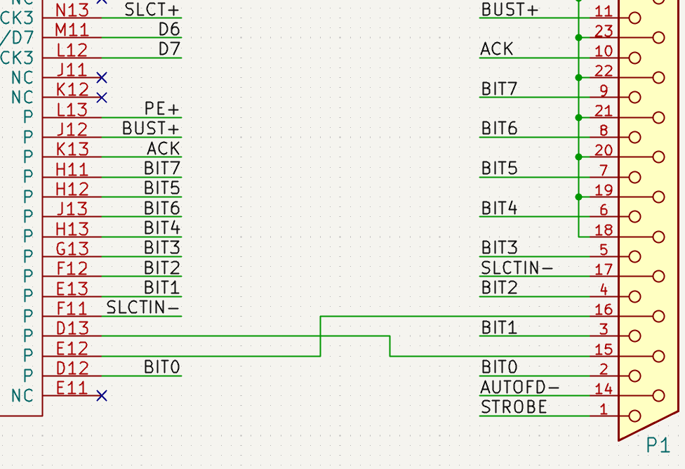
Wires that cross are not implicitly connected. It is necessary to join them by explicitly adding a junction dot if a connection is desired (![]() button in the right toolbar). Junction dots will be automatically added to wires that start or end on top of an existing wire.
button in the right toolbar). Junction dots will be automatically added to wires that start or end on top of an existing wire.
Junction dots are used in the schematic figure above on the wires connected to P1 pins 18, 19, 20, 21, 22, and 23.
Bus Connections
Buses are a way to group related signals in the schematic in order to simplify complicated designs. Buses can be drawn like wires using the bus tool ![]() , and are named using labels the same way signal wires are.
, and are named using labels the same way signal wires are.
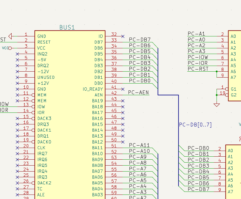
In the following schematic, many pins are connected to buses, which are the thick blue lines in the center.
Składniki magistral
There are two types of bus in KiCad 6.0 and later: vector buses and group buses.
Magistrala wektorowa to kolekcja sygnałów, których nazwa składa się z takiego samego przedrostka i kończy przyrostkiem z unikalną liczbą. Magistrale wektorowe są nazywane wg schematu <PREFIX>[M..N] gdzie PREFIX to dowolna nazwa sygnału, M to pierwsza liczba przyrostka, a N to ostatnia liczba. Na przykład, magistrala DATA[0..7] zawiera grupę sygnałów DATA0, DATA1, itd. aż do DATA7. Nie ma znaczenia jak wartości M oraz N zostały zdefiniowane, byle by nie były one wartościami ujemnymi.
Magistrala grupowa to kolekcja różnych sygnałów bądź magistral wektorowych. Magistrale grupowe można użyć do zgrupowania razem sygnałów posiadających różne nazwy. Magistrale grupowe używają specjalnego zapisu etykiet:
<OPTIONAL_NAME>{SIGNAL1 SIGNAL2 SIGNAL3}
Sygnały w grupie są wymienione wewnątrz nawiasów klamrowych ({}) oddzielonych spacjami. Opcjonalna nazwa grupy występuje przed otwierającym nawiasem klamrowym. Jeśli magistrala grupowa nie ma nazwy, wynikowe sieci w obwodzie drukowanym będą po prostu nazwami sygnałów wewnątrz grupy. Jeśli magistrala grupowa ma nazwę, wynikowe sieci będą miały nazwę jako prefiks z kropką (.) oddzielającą prefiks od nazwy sygnału.
Na przykład magistrala {SCL SDA} posiada dwa sygnały, stąd na liście sieci będą to sygnały SCL i ` SDA`. Magistrala USB1{DP DM} wygeneruje zaś sieci o nazwie USB1.DP i ` USB1.DM`. W przypadku projektów z większymi magistralami, które występują powtórnie w kilku podobnych obwodach, zastosowanie tej techniki może zaoszczędzić czas.
Magistrale grupowe mogą również zawierać magistrale wektorowe. Na przykład magistrala MEMORY{A[7..0] D[7..0] OE WE} zawiera zarówno magistrale wektorowe, jak i zwykłe sygnały co spowoduje utworzenie sieci takich jak: MEMORY.A7 i ` MEMORY.OE` na PCB.
Bus wires can be drawn and connected in the same manner as signal wires, including using junctions to create connections between crossing wires. Like signals, buses cannot have more than one name — if two conflicting labels are attached to the same bus, an ERC violation will be generated.
Połączenia pomiędzy składnikami magistral
Pins connected between the same members of a bus must be connected by labels. It is not possible to connect a pin directly to a bus; this type of connection will be ignored by KiCad.
W powyższym przykładzie, połączenia wykonane są za pomocą etykiet umieszczonych na połączeniach podłączonych do wyprowadzeń. Połączenia poprzez wejścia do magistral (odcinki połączeń pod kątem 45 stopni) mają wyłącznie wartość estetyczną, i nie są konieczne na poziomie czystego schematu.
In fact, using the repetition command (Insert), connections can be very quickly made in the following way, if component pins are aligned in increasing order (a common case in practice on components such as memories, microprocessors…):
-
Place the first label (for example
PCA0) -
Use the repetition command as much as needed to place members. KiCad will automatically create the next labels (
PCA1,PCA2…) vertically aligned, theoretically on the position of the other pins. -
Narysować połączenie pod pierwszą z etykiet. Następnie użyć polecenia powtarzania umieszczając dalsze połączenia pod etykietami.
-
W razie potrzeby umieścić wejścia do magistrali w ten sam sposób (Umieścić pierwsze wejście, a następnie użyć polecenia powtarzania).
|
In the Schematic Editor → Editing Options section of the Preferences menu, you can set the repetition parameters:
|
Wyprowadzanie sygnałów z magistral
The unfold tool allows you to quickly break out signals from a bus. To unfold a signal, right-click on a bus object (a bus wire, etc) and choose Unfold from Bus. Alternatively, use the Unfold Bus hotkey (default: C) when the cursor is over a bus object. The menu allows you to select which bus member to unfold.
Po wybraniu sygnału z magistrali, następne kliknięcie umieści etykietę sygnału magistrali w żądanym miejscu. Narzędzie automatycznie wygeneruje wejście do magistrali i połączenie prowadzące do miejsca gdzie znajdować się będzie etykieta. Po umieszczeniu etykiety możesz kontynuować umieszczanie dodatkowych segmentów połączenia (Na przykład, aby połączyć się z pinem komponentu) i dokończyć połączenie w dowolny sposób.
Aliasy magistral
Aliasy magistrali to skróty, które umożliwiają wydajniejszą pracę z magistralami o dużych grupach. Pozwalają one zdefiniować magistralę grupową i nadać jej krótką nazwę, która może być następnie używana zamiast pełnej nazwy grupy na schemacie.
To create bus aliases, open the Bus Definitions dialog in the Tools menu.
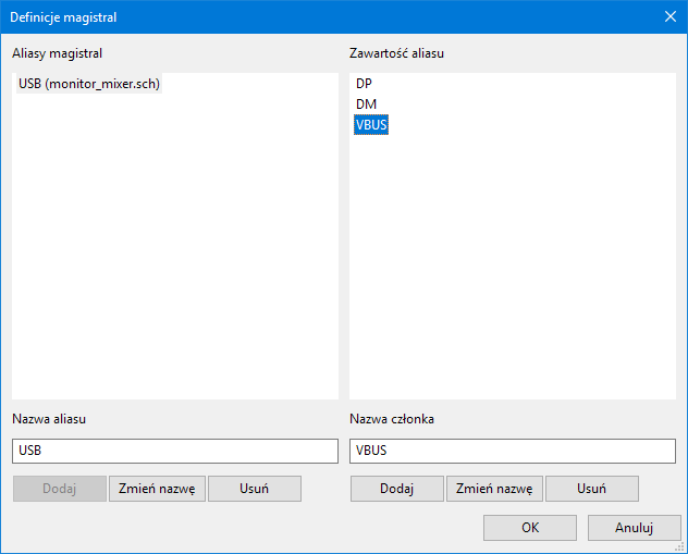
Alias może mieć dowolną dozwoloną nazwę sygnału. Korzystając z okna dialogowego, można dodawać sygnały lub magistrale wektorowe do aliasu. Jako skrót można wpisać lub wkleić listę sygnałów i/lub magistral oddzieloną spacjami, a wszystkie one zostaną dodane do definicji aliasu. W tym przykładzie zdefiniujemy alias o nazwie USB z elementami DP, DM i ` VBUS`.
Po zdefiniowaniu aliasu można go użyć jako etykiety magistrali grupowej, umieszczając nazwę aliasu w nawiasach klamrowych na magistrali grupowej: {USB}. Ma to taki sam efekt, jak etykietowanie magistrali {DP DM VBUS}. Można także dodać nazwę prefiksu do grupy, na przykład USB1 {USB}, co skutkuje nazwami sieci takimi jak USB1.DP, tak jak opisano to wcześniej. W przypadku skomplikowanych magistral używanie aliasów może znacznie skrócić etykiety na schemacie. Pamiętaj, że aliasy są tylko skrótem, a nazwa aliasu nie jest dołączana do listy sieci.
Aliasy magistral są zapisywane w pliku schematu. Wszelkie aliasy utworzone na danym arkuszu schematu są dostępne do użytku w dowolnym innym arkuszu schematu, który znajduje się w tej samej strukturze hierarchicznej.
Magistrale posiadające więcej niż jedną etykietę
Program KiCad w wersji 5.0 i wcześniejszych pozwalał na łączenie sygnałów magistral z różnymi etykietami i łączył je podczas tworzenia listy sieci. To zachowanie zostało usunięte w programie KiCad 6.0, ponieważ jest niekompatybilne z magistralami grupowymi, a także prowadzi do mylących list sieci, ponieważ nazwa którą dany sygnał odbierze, nie była do przewidzenia.
Jeśli otwarto projekt, który wykorzystywał tę funkcję w nowszej wersji programu, pojawi się okno dialogowe Migracja magistral, które przeprowadzi użytkownika przez aktualizację schematu, tak aby na danym zestawie sygnałów magistrali istniała tylko jedna etykieta.
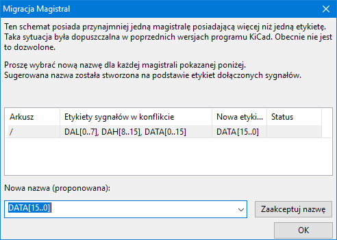
Dla każdego zestawu sygnałów magistrali, który ma więcej niż jedną etykietę, należy wybrać etykietę, która zostanie zachowana. Lista rozwijana z nazwami pozwala wybrać jedną z etykiet, istniejącą w projekcie lub wybrać inną nazwę, wprowadzając ją ręcznie w polu nowej nazwy.
Hidden Power Pins
When the power pins of a symbol are visible, they must be connected, as with any other signal. However, symbols such as gates and flip-flops are sometimes drawn with hidden power input pins which are connected implicitly.
KiCad automatically connects invisible pins with type "power input" to a global net with the same name as the pin. For example, if a symbol has a hidden power input pin named VCC, this pin will be globally connected to the VCC net on all sheets.
|
Hidden pins can be shown in the schematic by checking the Show hidden
pins option in the Schematic Editor → Display Options section
of the preferences, or by selecting View → Show hidden pins.
There is also a toggle icon |
It may be necessary to join power nets of different names (for example, GND in TTL components and VSS in MOS components). To accomplish this, add a power port symbol for each net and connect them with a wire.
If hidden power pins are used, it is not recommended to use local labels for power connection, as they will not connect to hidden power pins on other sheets.
| Care must be taken with hidden power input pins because they can create unintentional connections. By nature, hidden pins are invisible and do not display their pin name. This makes it easy to accidentally connect two power pins to the same net. For this reason, using invisible power pins in symbols is not recommended outside of power port symbols, and is only supported for compatibility with legacy designs and symbols. |
Power Ports
Power ports are symbols that are conventionally used to represent a connection to a power net, such as VCC or GND. In addition to being a visual indicator that the attached net is a power rail, power ports make global connections: two power ports with the same pin name connect to each other anywhere in the schematic, regardless of sheet.
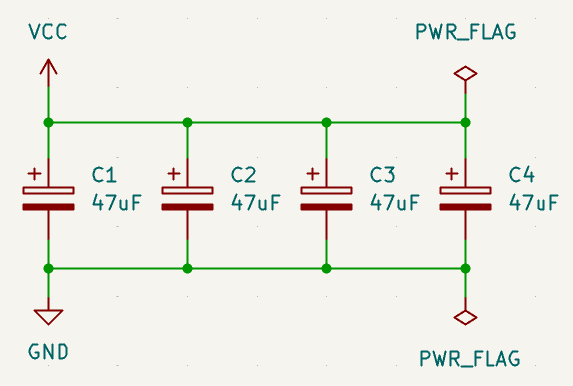
In the figure below, power port symbols are used to connect the positive and negative terminals of the capacitors to the VCC and GND nets, respectively.
In the KiCad standard library, power ports are found in the power library, but power port symbols can be created in any library. To create a custom power port, make a new symbol with a power input pin that is set to be invisible. Name the pin according to the desired power net. In addition, set the "Define as power symbol" symbol property. As described in the hidden power pins section, invisible power input pins make global connections based on the hidden power pin’s name. The process of creating a power port is described in more detail in the Symbol Editor section.
| The connected net name is determined by the power port’s pin name, not the name or value of the symbol. This means that power port net names can only be changed in the symbol editor, not in the schematic. |
Net name assignment rules
Every net in the schematic is assigned a name, whether that name is specified by the user or automatically generated by KiCad.
When multiple labels are attached to the same net, the final net name is determined in the following order, from highest priority to lowest:
-
Etykiety globalne
-
Local labels
-
Etykiety hierarchiczne
-
Hierarchical sheet pins
If there are multiple labels of one type attached to a net, the names are sorted alphabetically and the first is used.
If a net travels through multiple sheets in a hierarchy, and has no global label or power port, it will take its name from the highest level of the hierarchy where it has a hierarchical label or local label. As described above, local labels take priority over hierarchical labels.
If none of the labels above are attached to a net, the net’s name is automatically generated based on the connected symbol pins.
PWR_FLAG
Two PWR_FLAG symbols are visible in the screenshot above. They indicate to ERC that the two power nets VCC and GND are actually connected to a power source, as there is no explicit power source such as a voltage regulator output attached to either net.
Without these two flags, the ERC tool would diagnose: Error: Input Power pin not driven by any Output Power pins.
The PWR_FLAG symbol is found in the power symbol library. The same effect can be achieved by connecting any power output pin to the net.
No-connection flag
No-connection flags (![]() ) are used to indicate that a pin is intentionally unconnected. These flags do not have any effect on the schematic’s connectivity, but they prevent "unconnected pin" ERC warnings for pins that are intentionally unconnected.
) are used to indicate that a pin is intentionally unconnected. These flags do not have any effect on the schematic’s connectivity, but they prevent "unconnected pin" ERC warnings for pins that are intentionally unconnected.
Graphical items
Text and graphic lines
It can be useful to place annotations such as text fields and frames to aid in understanding the schematic. Text fields (![]() ) and graphic lines (
) and graphic lines (![]() ) are intended for this use, as opposed to labels and wires, which are connection elements.
) are intended for this use, as opposed to labels and wires, which are connection elements.
The image below shows graphic lines and text in addition to wires, local labels, and hierarchical labels.
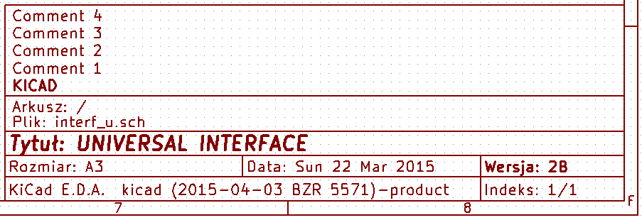
Tabelka
The title block is edited with the Page Settings tool (![]() ).
).
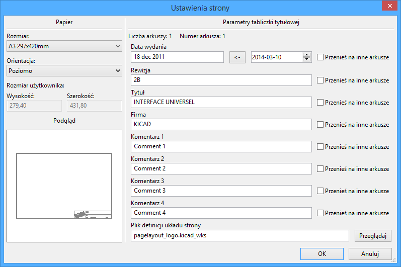
Each field in the title block can be edited, as well as the paper size and orientation. If the "Export to other sheets" option is checked for a field, that field will be updated in the title block of all sheets, rather than only the current sheet.
You can set the date to today’s or any other date by pressing the left arrow button by "Issue Date", but the date in the schematic will not be automatically updated.
A drawing sheet template file can also be selected.
The sheet number (Sheet X/Y) is automatically updated, but sheet page numbers can also be manually set using Edit → Edit Sheet Page Number….
Schematic Setup
The Schematic Setup window is used to set schematic options that are specific to the currently active schematic. For example, the Schematic Setup window contains formatting options, electrical rule configuration, netclass setup, and schematic text variable setup.
Odzyskiwanie symboli z pamięci cache
By default, KiCad loads symbols from the project libraries according to the set paths and library order. This can cause a problem when loading a very old project: if the symbols in the library have changed or have been removed or the library no longer exists since they were used in the project, the ones in the project would be automatically replaced with the new versions. The new versions might not line up correctly or might be oriented differently leading to a broken schematic.
When a project is saved, a cache library with the contents of the current library symbols is saved along with the schematic. This allows the project to be distributed without the full libraries. If you load a project where symbols are present both in its cache and in the system libraries, KiCad will scan the libraries for conflicts. Any conflicts found will be listed in the following dialog:
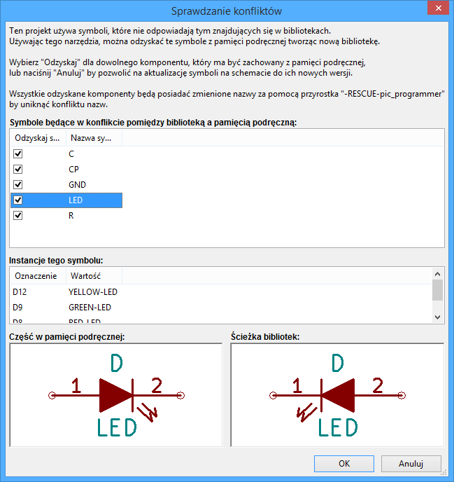
You can see in this example that the project originally used a diode with the cathode facing up, but the library now contains one with the cathode facing down. This change would break the schematic! Pressing OK here will cause the symbol cache library to be saved into a special rescue library and all the symbols are renamed to avoid naming conflicts.
If you press Cancel, no rescues will be made, so KiCad will load all the new components by default. If you save the schematic at this point, your cache will be overwritten and the old symbols will not be recoverable. If you have saved the schematic, you can still go back and run the rescue function again by selecting "Rescue Cached Components" in the "Tools" menu to call up the rescue dialog again.
Jeśli użytkownik nie chce by to okno dialogowe się pokazywało, może zaznaczyć opcję "Nie pokazuj ponownie". Będzie to oznaczało, że operacje porównania nie będą przeprowadzane i nowe symbole będą ładowane domyślnie. Opcję tą można wyłączyć w oknie ustawień bibliotek.
Schematy o strukturze hierarchicznej
Wprowadzenie
In KiCad, multi-sheet schematics are hierarchical: there is a single root sheet, and additional sheets are created as subsheets of either the root sheet or another subsheet. Sheets can be included in a hierarchy multiple times, if desired.
Carefully drawing a schematic as a hierarchical design improves schematic legibility and reduces repetitive drawing.
Creating a hierarchical schematic starts from the root sheet. The process is to create a subsheet, then draw the circuit in the subsheet and make the necessary electrical connections between sheets. Connections can be made between nets in a subsheet and nets in the parent sheet using hierarchical pins and labels, or between any two nets in the hierarchy using global labels.
Adding sheets to a design
You can add a subsheet to a design with the Add Hierarchical Sheet tool (S hotkey, or the ![]() button in the right toolbar). Launch the tool, then click twice in the canvas to draw the upper left and lower right corners of the subsheet symbol. Make the sheet outline large enough to fit the hierarchical pins you will add later.
button in the right toolbar). Launch the tool, then click twice in the canvas to draw the upper left and lower right corners of the subsheet symbol. Make the sheet outline large enough to fit the hierarchical pins you will add later.
The Sheet Properties dialog will appear and prompt you for a sheet name and filename.
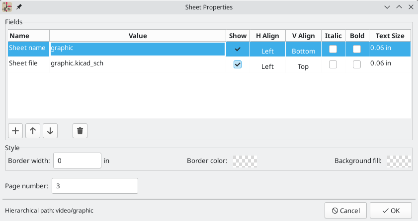
The sheet name must be unique, as it is used in the full net name for any nets in the subsheet. For example, a net with the local label net1 in the sheet sheet1 would have a full net name of /sheet1/net1. The sheet name is also used to refer to the sheet in various places in the GUI, including the title block and the hierarchy navigator.
The sheet filename specifies the file that the new sheet will be saved to or loaded from. The path to the sheet file can be relative or absolute. It is usually preferable to save subsheet files in the project directory and use a relative path so that the project is portable.
A single sheet file can be used more than once in a project by specifying the same filename for each repeated sheet; the circuit drawn in the sheet will be instantiated once per usage, and any edits in once instance will be reflected in the other instances.
| Sheet files can be shared between multiple projects to allow design reuse between projects. However, this is not recommended due to path portability concerns and the risk of unintentionally changing other projects while editing a shared sheet. |
The sheet’s page number is configurable here. The page number is displayed in the sheet title block and the hierarchy navigator, and sheets are sorted by page number in the hierarchy navigator and when printing or plotting.
Several graphical options are also available. Border width sets the width of the border around the sheet shape. Border color and Background fill set the color for the border and fill of the sheet shape, respectively. If no color is set, a checkerboard swatch is shown and the default values from the color theme are used.
The Sheet Properties dialog can be accessed at any time by selecting a sheet symbol and using the E hotkey, or by right-clicking on a sheet symbol and selecting Properties….
Navigating between sheets
You can enter a hierarchical sheet from the parent sheet by double-clicking the child sheet’s shape, or right-clicking the child sheet and selecting Enter Sheet.
Return to the parent sheet by using the ![]() button in the top toolbar, or by right-clicking in an empty part of the schematic and clicking Leave Sheet.
button in the top toolbar, or by right-clicking in an empty part of the schematic and clicking Leave Sheet.
Alternatively, you can jump to any sheet with the hierarchy navigator. To open the hierarchy navigator, click the ![]() button in the top toolbar. Each sheet in the design is displayed as an item in the tree. Clicking a sheet name opens that sheet in the editing canvas.
button in the top toolbar. Each sheet in the design is displayed as an item in the tree. Clicking a sheet name opens that sheet in the editing canvas.
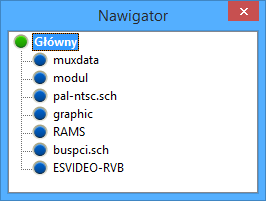
By default, the hierarchy navigator closes after a new sheet is opened. It can be configured to always remain open by selecting the Keep hierarchy navigator open option in the Editing Options section of the Schematic Editor preferences.
Electrical connections between sheets
Label overview
Electrical connections between sheets are made with labels. There are several kinds of labels in KiCad, each with a different connection scope.
-
Local labels only make connections within a sheet. Therefore local labels cannot be used to connect between sheets. Local labels are added with the
button. -
Global labels make connections anywhere in a schematic, regardless of sheet. Global labels are added with the
button. -
Hierarchical labels connect to hierarchical sheet pins accessible in the parent sheet. Hierarchical designs rely on hierarchical labels and pins to make connections between parent sheets and child sheets; you can think of hierarchical pins as defining the interface for a sheet. Hierarchical labels are added with the
button.
| Labels that have the same name will connect, regardless of the label type, if they are in the same sheet. |
| Hidden power pins can also be considered global labels, because they connect anywhere in the schematic hierarchy. |
Hierarchical sheet pins
After placing hierarchical labels within the subsheet, matching hierarchical pins can be added to the subsheet symbol in the parent sheet. You can then make connections to the hierarchical pins with wires, labels, and buses. Hierarchical pins in a subsheet symbol are connected to the matching hierarchical labels in the subsheet itself.
| Hierarchical labels must be defined in the subsheet before the corresponding hierarchical sheet pin can be imported in the sheet symbol. |
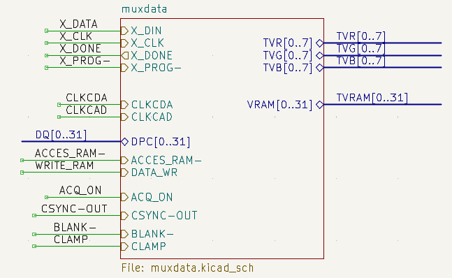
For every hierarchical label in the subsheet, import the corresponding hierarchical pin into the sheet symbol by clicking the ![]() button in the right toolbar, then clicking on the sheet symbol. A sheet pin for the first unmatched hierarchical label will be attached to the cursor, where it can be placed anywhere along the border of the sheet symbol. Clicking again with the tool will continue to import additional sheet pins until there are no more hierarchical pins to import from the subsheet. Sheet pins can also be imported by selecting Import Sheet Pin in a sheet symbol’s right-click context menu.
button in the right toolbar, then clicking on the sheet symbol. A sheet pin for the first unmatched hierarchical label will be attached to the cursor, where it can be placed anywhere along the border of the sheet symbol. Clicking again with the tool will continue to import additional sheet pins until there are no more hierarchical pins to import from the subsheet. Sheet pins can also be imported by selecting Import Sheet Pin in a sheet symbol’s right-click context menu.
You can edit the properties of a sheet pin in the Sheet Pin Properties dialog. Open this dialog by double-clicking a sheet pin, selecting a sheet pin and using the E hotkey, or right-clicking a sheet pin and selecting Properties….
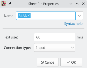
The sheet pin’s name can be edited in the textbox or by selecting from the dropdown list of hierarchical labels in the subsheet. A sheet pin’s name has to match the corresponding hierarchical label in the subsheet, so if a pin name is changed the label must change as well.
The connection type changes the shape of the sheet pin, and has no electrical effect. It can be set to Input, Output, Bidirectional, Tri-state, or Passive. The pin’s text size can also be changed.
Hierarchical design examples
Hierarchical designs can be put into one of several categories:
-
Simple: each sheet is used only once.
-
Complex: some sheets are instantiated multiple times.
-
Flat: a sub-case of a simple hierarchy, without connections between subsheets and their parent. Flat hierarchies can be used to represent a non-hierarchical design.
Each hierarchy model can be useful; the most appropriate one depends on the design.
Simple hierarchy
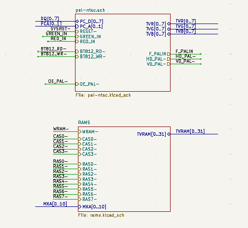
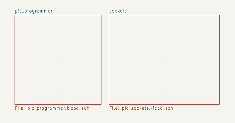
An example of a simple hierarchy is the video demo project included with KiCad. The root sheet contains seven unique subsheets, each with hierarchical labels and sheet pins linking the sheets to each other in the root sheet. Two of the subsheet symbols are shown below.
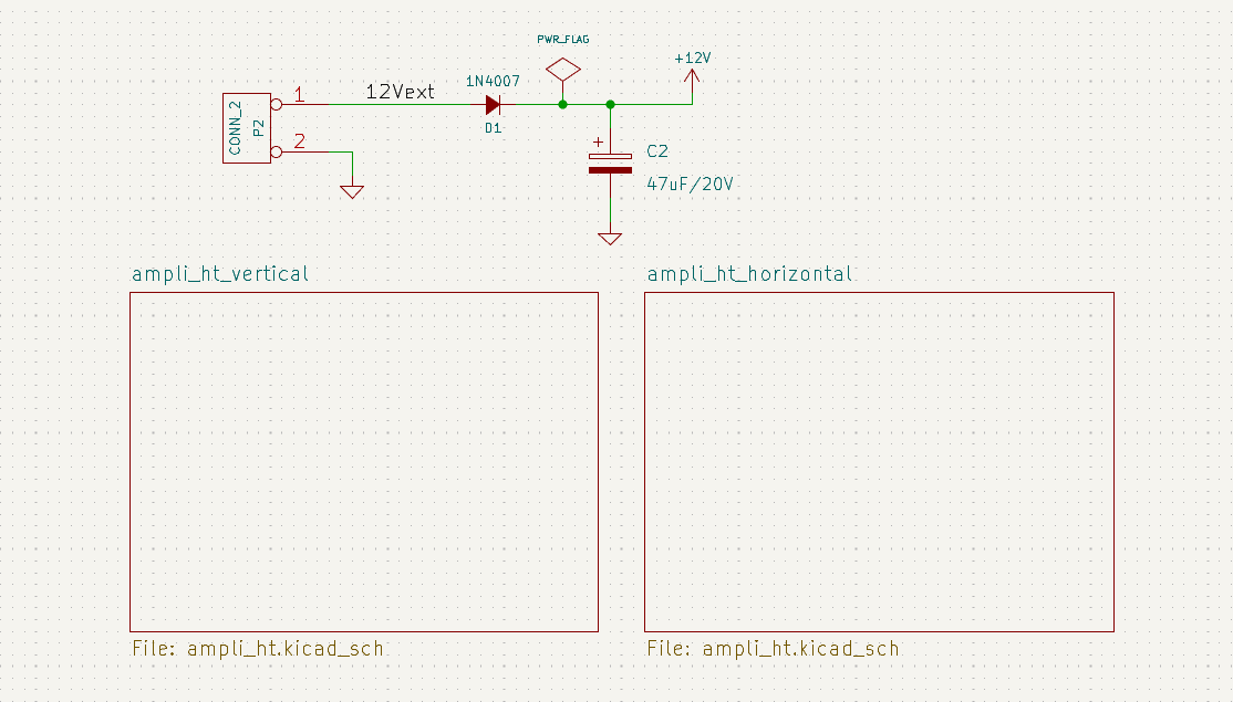
Hierarchia złożona
The complex_hierarchy demo project is an example of a complex hierarchy. The root sheet contains two subsheet symbols, which both refer to the same sheet file (ampli_ht.kicad_sch). This allows the design to include two copies of the same amplifier circuit. Although the two sheet symbols refer to the same filename, the sheet names are unique (ampli_ht_vertical and ampli_ht_horizontal). Inside each subsheet the circuits are identical except for the reference designators, which as always are unique.
This project contains no sheet pin connections. The only connections between the root sheet and the subsheets are global power connections made with power port symbols. However, sheets in a complex hierarchy could include sheet pin connections if appropriate for the design.
Hierarchia płaska
The flat_hierarchy demo project is an example of a flat hierarchy. The root sheet contains two unique subsheet symbols with no hierarchical sheet pins. The root sheet in this project does nothing except hold the subsheets, and the subsheets are used only as additional pages in the schematic.
| This is the simplest way to create multi-page schematics in KiCad. |
Inspecting a schematic
Find tool
The Find tool searches for text in the schematic, including reference designators, pin names, symbol fields, and graphic text. When the tool finds a match, the canvas is zoomed and centered on the match and the text is highlighted. Launch the tool using the ![]() button in the top toolbar.
button in the top toolbar.
The Find tool has several options:
Match case: Selects whether the search is case-sensitive.
Words: When selected, the search will only match the search term with complete words in the schematic. When unselected, the search will match if the search term is part of a larger word in the schematic.
Wildcards: When selected, wildcards can be used in the search terms. ?
matches any single character, and * matches any number of characters. Note
that when this option is selected, partial matches are not returned: searching
for abc* will match the string abcd, but searching for abc will not.
Search pin names and numbers: Selects whether the search should apply to pin names and numbers.
Search hidden fields: Selects whether the search should apply only to visible fields or if it should include hidden symbol fields.
Search the current sheet only: Selects whether the search should be limited to the current schematic sheet or to the entire schematic.
There is also a Find and Replace tool which is activated with the ![]() button in the top toolbar. This tool behaves the same as the Find tool, but additionally can replace some or all matches with different text.
button in the top toolbar. This tool behaves the same as the Find tool, but additionally can replace some or all matches with different text.
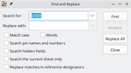
If the Replace matches in reference designators option is checked, reference designators will be modified if they contain matching text. Otherwise reference designators will not be affected.
Net highlighting
An electrical net can be highlighted in the schematic editor to visualize all of the places it appears in the schematic. Net highlighting can be activated in the Schematic Editor or by highlighting the corresponding net in the PCB editor when cross-probe highlighting is enabled (see below). When net highlighting is active, the highlighted net will be shown in a different color. By default this color is pink, but it is configurable in the Color section of the Preferences dialog.
Nets can be highlighted by clicking on a wire or pin using the Highlight Net tool in the right toolbar (![]() ). Alternatively, the Highlight Net hotkey (`) highlights the net under the cursor. If there are no nets or pins under the cursor, any existing highlighting will be cleared. The highlighting can also be cleared by using the Clear Net Highlight action (hotkey ~).
). Alternatively, the Highlight Net hotkey (`) highlights the net under the cursor. If there are no nets or pins under the cursor, any existing highlighting will be cleared. The highlighting can also be cleared by using the Clear Net Highlight action (hotkey ~).
Cross-probing from the PCB
KiCad allows bi-directional cross-probing between the schematic and the PCB. There are several different types of cross-probing.
Selection cross-probing allows you to select a symbol or pin in the schematic to select the corresponding footprint or pad in the PCB (if one exists) and vice-versa. By default, cross-probing will result in the display centering on the cross-probed item and zooming to fit. This behavior can be disabled in the Display Options section of the Preferences dialog.
Highlight cross-probing allows you to highlight a net in the schematic and PCB at the same time. If the option "Highlight cross-probed nets" is enabled in the Display Options section of the Preferences dialog, highlighting a net or bus in the schematic editor will cause the corresponding net or nets to be highlighted in the PCB editor, and vice versa.
Kontrola reguł projektowych - Electrical Rules Check
The Electrical Rules Check (ERC) tool performs an automatic check of your schematic. The ERC checks for any errors in your sheet, such as unconnected pins, unconnected hierarchical symbols, shorted outputs, etc. ERC output is reported as errors or warnings depending on the severity of the issue detected.
Naturally, an automatic check is not infallible, and it is not possible to detect all design errors. Such a check is still very useful, because it allows you to detect many oversights and small errors. All detected issues should be checked and addressed before proceeding.
The quality of the ERC is directly related to the care taken in declaring electrical pin properties during symbol library creation.
ERC can be started by clicking on the ![]() button in the top toolbar and clicking the Run ERC button.
button in the top toolbar and clicking the Run ERC button.
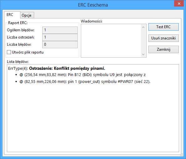
Any warnings or errors are reported in the Violations tab, and markers for each violation are placed in the schematic so that they point to the relevant part of the schematic. Warnings are indicated by yellow arrows, and errors have red arrows. Excluded violations are shown as green arrows.
| Selecting a violation in the ERC window jumps to the selected violation marker in the schematic. |
The numbers at the bottom of the window show the number of errors, warnings, and exclusions. Each type of violation can be filtered from the list using the respective checkboxes. Clicking Delete Markers will clear all violations until ERC is run again.
Violations can be right-clicked in the dialog to ignore them or change their severity:
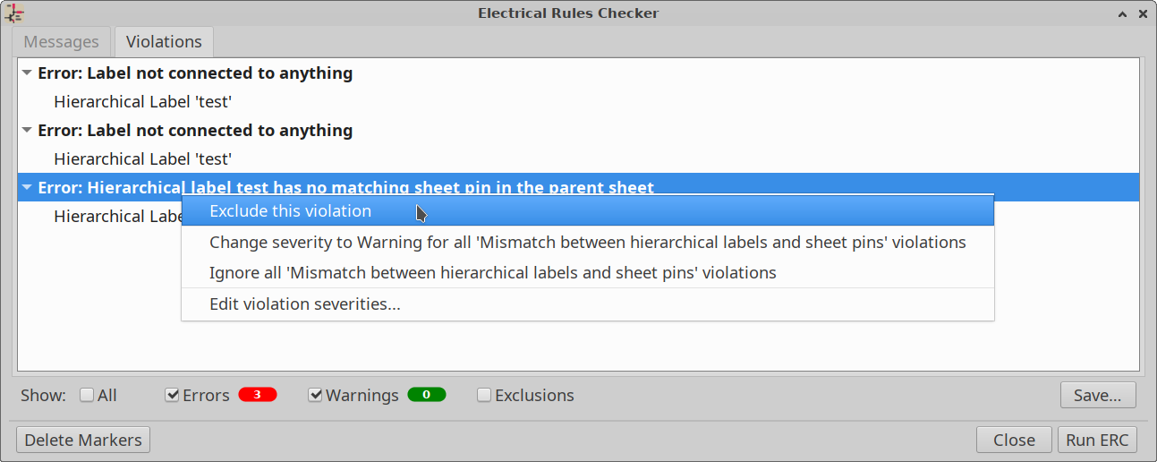
-
Exclude this violation: ignores this particular violation, but does not affect any other violations.
-
Change severity: changes a type of violation from warning to error, or error to warning. This affects all violations of a given type.
-
Ignore all: ignores all violations of a given type.
ERC example
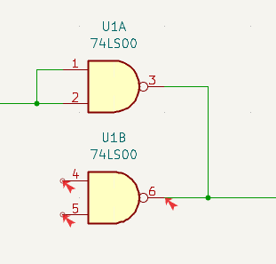
Here you can see three errors:
-
Two outputs have been connected together (red arrow at right).
-
Two inputs have been left unconnected (red arrows at left).
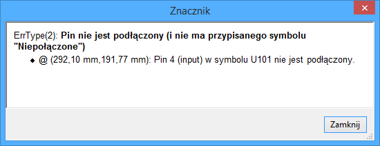
Selecting an ERC marker displays a description of the violation in the message pane at the bottom of the window.
Power pins and power flags
It is common to have an "Input Power pin not driven by any Output Power pins" error on power pins, as shown in the example below, even though the power pins seem to be properly connected to a power rail. This happens in designs where the power is provided through connectors or other components that are not marked as power outputs. In these cases ERC won’t detect any Output Power pins connected to the net and will determine the Input Power pin is not driven by a power source.
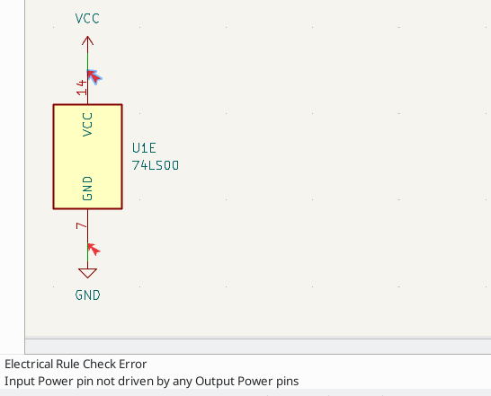
To avoid this warning, connect the net to PWR_FLAG symbol on such a power net as shown in the following example. The PWR_FLAG symbol is found in the power symbol library. Alternatively, connect any power output pin to the net; PWR_FLAG is simply a symbol with a single power output pin.
Ground nets often need a PWR_FLAG as well, because voltage regulators have outputs declared as power outputs, but their ground pins are typically marked as power inputs. Therefore grounds can appear unconnected to a source unless a PWR_FLAG symbol is used.
For more information about power pins and power flags, see the PWR_FLAG documentation.
ERC Configuration
The Pin Conflicts Map panel in Schematic Setup allows you to configure connectivity rules to define electrical conditions for errors and warnings based on what types of pins are connected to each other.
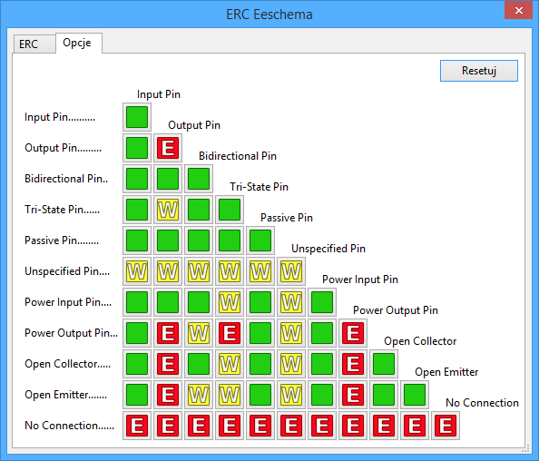
Poszczególne reguły mogą zostać zmienione poprzez kliknięcie na wybranym polu na powyższej matrycy. Kolejne kliknięcia pozwalają na wybranie: brak błędu (zielony), ostrzeżenie (żółty, W) i błąd (czerwony, E). Zmiany odbywają się w zamkniętym cyklu, zatem aby wrócić do poprzedniego stanu należy ponownie kliknąć (jedno- lub dwukrotnie).
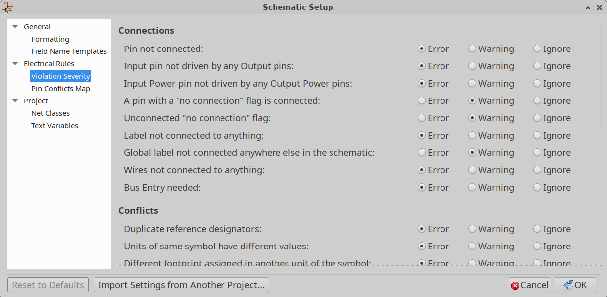
The Violation Severity panel in Schematic Setup lets you configure what types of ERC messages should be reported as Errors, Warnings or ignored.
Plik raportu ERC
An ERC report file can be generated and saved by clicking the Save… button in the ERC dialog. The file extension for ERC report files is .rpt. Here is an example ERC report file.
ERC report (Fri 21 Oct 2022 02:07:05 PM EDT, Encoding UTF8)

***** Sheet /
[pin_not_driven]: Input pin not driven by any Output pins
    ; Severity: error
    @(149.86 mm, 60.96 mm): Symbol U1B [74LS00] Pin 4 [, Input, Line]
[pin_not_connected]: Pin not connected
    ; Severity: error
    @(149.86 mm, 60.96 mm): Symbol U1B [74LS00] Pin 4 [, Input, Line]
[pin_not_connected]: Pin not connected
    ; Severity: error
    @(149.86 mm, 66.04 mm): Symbol U1B [74LS00] Pin 5 [, Input, Line]
[pin_to_pin]: Pins of type Output and Output are connected
    ; Severity: error
    @(165.10 mm, 63.50 mm): Symbol U1B [74LS00] Pin 6 [, Output, Inverted]
    @(165.10 mm, 46.99 mm): Symbol U1A [74LS00] Pin 3 [, Output, Inverted]
[pin_not_driven]: Input pin not driven by any Output pins
    ; Severity: error
    @(149.86 mm, 66.04 mm): Symbol U1B [74LS00] Pin 5 [, Input, Line]

 ** ERC messages: 5  Errors 5  Warnings 0
Assigning Footprints
Before routing a PCB, footprints need to be selected for every component that will be assembled on the board. Footprints define the copper connections between physical components and the routed traces on a circuit board.
Some symbols come with footprints pre-assigned, but for many symbols there are multiple possible footprints, so the user needs to select the appropriate one.
KiCad offers several ways to assign footprints:
-
Właściwości symbolu
-
Symbol Properties Dialog
-
Symbol Fields Table
-
-
While placing symbols
-
Footprint Assignment Tool
Each method will be explained below. Which to use is a matter of preference; one method may be more convenient depending on the situation. All of these methods are equivalent in that they store the name of the selected footprint in the symbol’s Footprint field.
| The Footprint Library Table needs to be configured before footprints can be assigned. For information on configuring the Footprint Library Table, please see the PCB Editor manual. |
Assigning Footprints in Symbol Properties
A symbol’s Footprint field can be edited directly in the symbol’s Properties window.
Clicking the ![]() button in the
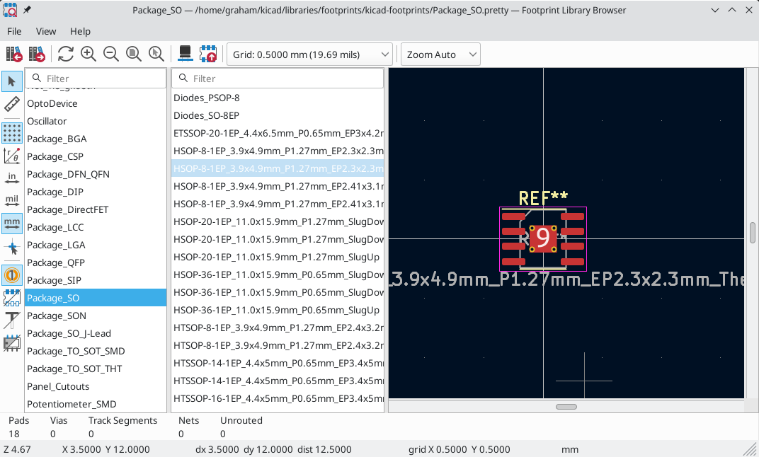
button in the Footprint field opens the Footprint Library Browser, which shows the available footprints and footprint libraries. Single clicking a footprint name selects the footprint and displays it in the preview pane on the right, while double clicking on a footprint closes the browser and sets the symbol’s Footprint field to the selected footprint.
Assigning Footprints with the Symbol Fields Table
Rather than editing the properties of each symbol individually, the Symbol Fields Table can be used to view and edit the properties of all symbols in the design in one place. This includes assigning footprints by editing the Footprint field of each symbol.
The Symbol Fields Table is accessed with Tools → Edit Symbol Fields…, or with the ![]() button on the top toolbar.
button on the top toolbar.
The Footprint field behaves the same here as in the Symbol Properties window: it can be edited directly, or footprints can be selected visually with the Footprint Library Browser.
For more information on the Symbol Fields Table, see the section on editing symbol properties.
Assigning Footprints While Placing Symbols
Footprints can be assigned to symbols when the symbol is first added to the schematic.
Some symbols are defined with a default footprint. These symbols will have this footprint preassigned when they are added to the schematic. The default footprint is shown in the Add Symbol dialog. For symbols without a default symbol defined, the footprint dropdown will say "No default footprint", and the footprint preview canvas will say "No footprint specified".
Symbols can have footprint filters that specify which footprints are appropriate to use with that symbol. If footprint filters are defined for the selected symbol, all footprints that match the footprint filters will appear as options in the footprint dropdown. The selected footprint will be displayed in the preview canvas and will be assigned to the symbol when the symbol is added to the schematic.
| Footprint options will not appear in the footprint dropdown unless the footprint libraries are loaded. Footprint libraries are loaded the first time the Footprint Editor or Footprint Library Browser are opened in a session. |
For more information on footprint filters, see the Symbol Editor Documentation.
Assigning Footprints with the Footprint Assignment Tool
The Footprint Assignment Tool allows you to associate symbols in your schematic to footprints used when laying out the printed circuit board. It provides footprint list filtering, footprint viewing, and 3D component model viewing to help ensure the correct footprint is associated with each component.
Components can be assigned to their corresponding footprints manually or automatically by creating equivalence files (.equ files). Equivalence files are lookup tables associating each component with its footprint.
Run the tool with Tools → Assign Footprints…, or by clicking the ![]() icon in the top toolbar.
icon in the top toolbar.
Footprint Assignment Tool Overview
The image below shows the main window of the Footprint Assignment Tool.
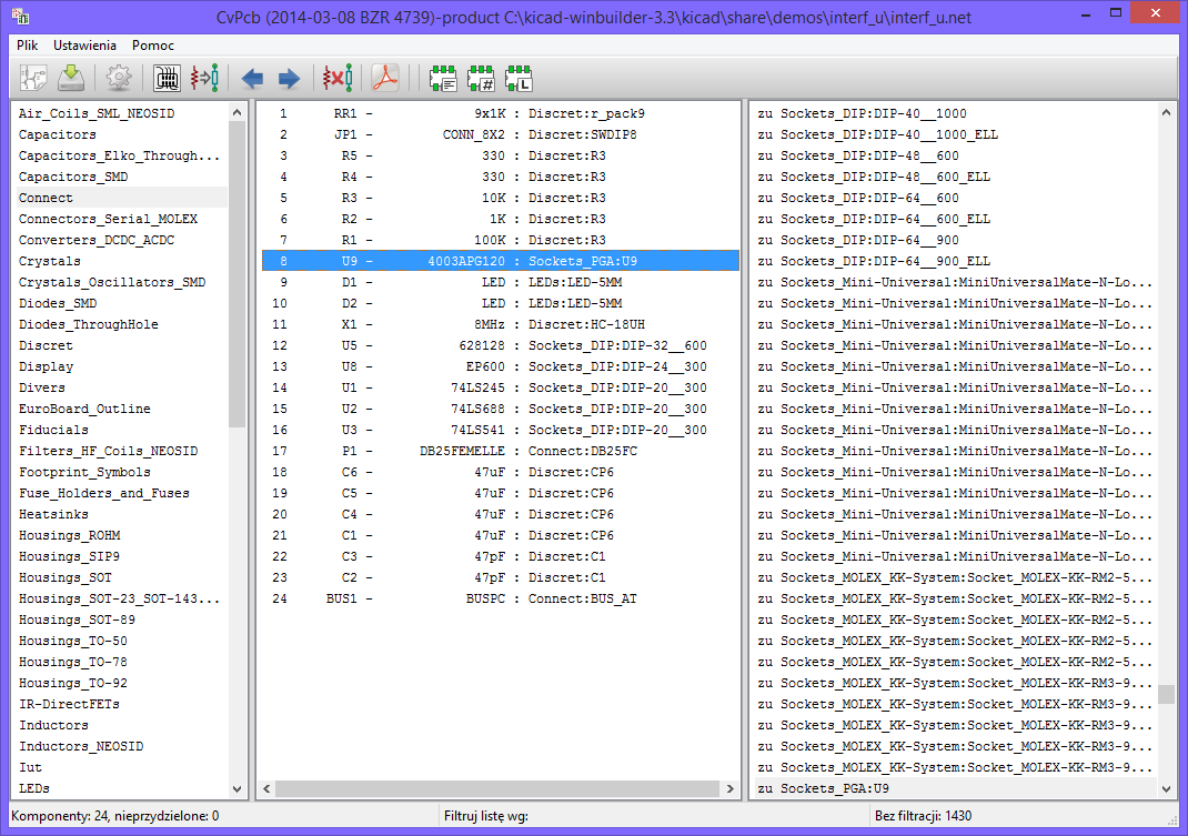
-
The left pane contains the list of available footprint libraries associated with the project.
-
The center pane contains the list of symbols in the schematic.
-
The right pane contains the list of available footprints loaded from the project footprint libraries.
-
The bottom pane describes the filters that have been applied to the footprint list and prints information about the footprint selected in the rightmost pane.
The top toolbar contains the following commands:
|
Transfer the current footprint associations to the schematic. |
|
Edit the global and project footprint library tables. |
|
View the selected footprint in the footprint viewer. |
|
Select the previous symbol without a footprint association. |
|
Select the next symbol without a footprint association. |
|
Undo last edit. |
|
Redo last edit. |
|
Perform automatic footprint association using an equivalence file. |
|
Delete all footprint assignments. |
|
Filter footprint list by footprint filters defined in the selected symbol. |
|
Filter footprint list by pin count of the selected symbol. |
|
Filter footprint list by selected library. |
The following table lists the keyboard commands for the Footprint Assignment Tool:
Right Arrow / Tab |
Activate the pane to the right of the currently activated pane. Wrap around to the first pane if the last pane is currently activated. |
Left Arrow |
Activate the pane to the left of the currently activated pane. Wrap around to the last pane if the first pane is currently activated. |
Up Arrow |
Select the previous item of the currently selected list. |
Down Arrow |
Select the next item of the currently selected list. |
Page Up |
Select the item one full page upwards of the currently selected item. |
Page Down |
Select the item one full page downwards of the currently selected item. |
Home |
Select the first item of the currently selected list. |
End |
Select the last item of the currently selected list. |
Manually Assigning Footprints with the Footprint Assignment Tool
To manually associate a footprint with a component, first select a component in the component (middle) pane. Then select a footprint in the footprint (right) pane by double-clicking on the name of the desired footprint. The footprint will be assigned to the selected component, and the next component without an assigned footprint is automatically selected.
| If no footprints appear in the footprint pane, check that the footprint filter options are correctly applied. |
When all components have footprints assigned to them, click the OK button to save the assignments and exit the tool. Alternatively, click Cancel to discard the updated assignments, or Apply, Save Schematic & Continue to save the new assignments without exiting the tool.
Filtrowanie listy footprintów
There are four filtering options which restrict which footprints are displayed in the footprint pane. The filtering options are enabled and disabled with three buttons and a textbox in the top toolbar.
-
 : Activate filters that can be defined in each symbol. For example, an opamp symbol might define filters that show only SOIC and DIP footprints.
 -
 : Only show footprints that match the selected symbol’s pin count.
 -
 : Only show footprints from the library selected in the left pane.
 -
Entering text in the textbox hides footprints that do not match the text. This filter is disabled when the box is empty.
When all filters are disabled, the full footprint list is shown.
The applied filters are described in the bottom pane of the window, along with the number of footprints that meet the selected filters. For example, when the symbol’s footprint filters and pin count filters are enabled, the bottom pane prints the footprint filters and pin count:
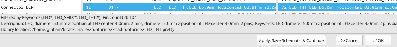
Multiple filters can be used at once to help narrow down the list of possibly appropriate footprints in the footprint pane. The symbols in KiCad’s standard library define footprint filters that are designed to be used in combination with the pin count filter.
Automatically Assigning Footprints with the Footprint Assignment Tool
The Footprint Assignment Tool allows you to store footprint assignments in an external file and load the assignments later, even in a different project. This allows you to automatically associate symbols with the appropriate footprints.
The external file is referred to as an equivalence file, and it stores a mapping of a symbol value to a corresponding footprint. Equivalence files typically use the .equ file extension. Equivalence files are plain text files with a simple syntax, and must be created by the user using a text editor. The syntax is described below.
You can select which equivalence files to use by clicking Preferences → Manage Footprint Association Files in the Footprint Assignment Tool.
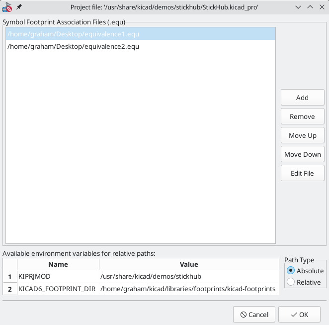
-
Add new equivalence files by clicking the Add button.
-
Remove the selected equivalence file by clicking the Remove button.
-
Change the priority of equivalence files by clicking the Move Up and Move Down buttons. If a symbol’s value is found in multiple equivalence files, the footprint from the last matching equivalence file will override earlier equivalence files.
-
Open the selected equivalence file by clicking the Edit File button.
Relevant environment variables are shown at the bottom of the window. When the Relative path option is checked, these environment variables will automatically be used to make paths to selected equivalence files relative to the project or footprint libraries.
Once the desired equivalence files have been loaded in the correct order, automatic footprint association can be performed by clicking the ![]() button in the top toolbar of the Footprint Assignment Tool.
button in the top toolbar of the Footprint Assignment Tool.
All symbols with a value found in a loaded equivalence file will have their footprints automatically assigned. However, symbols that already have footprints assigned will not be updated.
Format plików
Equivalence files consist of one line for each symbol value. Each line has the following structure:
'<symbol value>' '<footprint library>:<footprint name>'
Each name/value must be surrounded by single quotes (') and separated by one or more spaces. Lines starting with # are comments.
For example, if you want all symbols with the value LM4562 to be assigned the footprint Package_SO:SOIC-8_3.9x4.9_P1.27mm, the line in the equivalence file should be:
'LM4562' 'Package_SO:SOIC-8_3.9x4.9_P1.27mm'
Poniżej znajduje się przykład pliku przypisań:
#integrated circuits (smd):
'74LV14' 'Package_SO:SOIC-14_3.9x8.7mm_P1.27mm'
'EL7242C' 'Package_SO:SOIC-8_3.9x4.9_P1.27mm'
'DS1302N' 'Package_SO:SOIC-8_3.9x4.9_P1.27mm'
'LM324N' 'Package_SO:SOIC-14_3.9x8.7mm_P1.27mm'
'LM358' 'Package_SO:SOIC-8_3.9x4.9_P1.27mm'
'LTC1878' 'Package_SO:MSOP-8_3x3mm_P0.65mm'
'24LC512I/SM' 'Package_SO:SOIC-8_3.9x4.9_P1.27mm'
'LM2903M' 'Package_SO:SOIC-8_3.9x4.9_P1.27mm'
'LT1129_SO8' 'Package_SO:SOIC-8_3.9x4.9_P1.27mm'
'LT1129CS8-3.3' 'Package_SO:SOIC-8_3.9x4.9_P1.27mm'
'LT1129CS8' 'Package_SO:SOIC-8_3.9x4.9_P1.27mm'
'LM358M' 'Package_SO:SOIC-8_3.9x4.9_P1.27mm'
'TL7702BID' 'Package_SO:SOIC-8_3.9x4.9_P1.27mm'
'TL7702BCD' 'Package_SO:SOIC-8_3.9x4.9_P1.27mm'
'U2270B' 'Package_SO:SOIC-16_3.9x9.9_P1.27mm'

#regulators
'LP2985LV' 'Package_TO_SOT_SMD:SOT-23-5_HandSoldering'
Podgląd bieżącego footprintu
The Footprint Assignment Tool contains a footprint viewer. Clicking the ![]() button in the top toolbar launches the footprint viewer and shows the selected footprint.
button in the top toolbar launches the footprint viewer and shows the selected footprint.
The top toolbar contains the following commands:
|
Refresh view |
|
Zoom in |
|
Zoom out |
|
Zoom to fit drawing in display area |
|
Show 3D viewer |
The left toolbar contains the following commands:
|
Use the select tool |
|
Interactively measure between two points |
|
Display grid dots or lines |
|
Switch between polar and cartesian coordinate systems |
|
Use inches |
|
Display coordinates in mils (1/1000 of an inch) |
|
Display coordinates in millimeters |
|
Toggle display of full-window crosshairs |
|
Toggle between drawing pads in sketch or normal mode |
|
Toggle between drawing pads in normal mode or outline mode |
|
Toggle between drawing text in normal mode or outline mode |
|
Toggle between drawing graphic lines in normal mode or outline mode |
Podgląd bieżącego modelu 3D
Clicking the ![]() button opens the footprint in the 3D model viewer.
button opens the footprint in the 3D model viewer.
| If a 3D model does not exist for the current footprint, only the footprint itself will be shown in the 3D Viewer. |
The 3D Viewer is described in the PCB Editor manual.
Transferring designs between schematic and PCB
Update PCB from Schematic
Use the Update PCB from Schematic tool to sync design information from the Schematic Editor to the Board Editor. The tool can be accessed with Tools → Update PCB from Schematic (F8) in both the schematic and board editors. You can also use the ![]() icon in the top toolbar of the Board Editor.
icon in the top toolbar of the Board Editor.
| Update PCB from Schematic is the preferred way to transfer design information from the schematic to the PCB. In older versions of KiCad, the equivalent process was to export a netlist from the Schematic Editor and import it into the Board Editor. It is no longer necessary to use a netlist file. |
The tool adds the footprint for each symbol to the board and transfers updated schematic information to the board. In particular, the board’s net connections are updated to match the schematic.
The changes that will be made to the PCB are listed in the Changes To Be Applied pane. The PCB is not modified until you click the Update PCB button.
You can show or hide different types of messages using the checkboxes at the bottom of the window. A report of the changes can be saved to a file using the Save… button.
Options
The tool has several options to control its behavior.
| Option | Description |
|---|---|
Re-link footprints to schematic symbols based on their reference designators |
Footprints are normally linked to schematic symbols via a unique identifier created when the symbol is added to the schematic. A symbol’s unique identifier cannot be changed. If checked, each footprint in the PCB will be re-linked to the symbol that has the same reference designator as the footprint. If unchecked, footprints and symbols will be linked by unique identifier as usual, rather than by reference designator. Each footprint’s reference designator will be updated to match the reference designator of its linked symbol. This option should generally be left unchecked. It is useful for specific workflows that rely on changing the links between schematic symbols and footprints, such as refactoring a schematic for easier layout or replicating layout between identical channels of a design. |
Delete footprints with no symbols |
If checked, any footprint in the PCB without a corresponding symbol in the schematic will be deleted from the PCB. Footprints with the "Not in schematic" attribute will be unaffected. If unchecked, footprints without a corresponding symbol will not be deleted. |
Replace footprints with those specified in the schematic |
If checked, footprints in the PCB will be replaced with the footprint that is specified in the corresponding schematic symbol. If unchecked, footprints that are already in the PCB will not be changed, even if the schematic symbol is updated to specify a different footprint. |
Update Schematic from PCB
| TODO: write this section |
Backannotation with CMP files
Select changes can also be synced from the PCB back to the schematic by exporting a CMP file from the PCB editor (File → Export → Footprint Association (.cmp) File…) and importing it in the Schematic Editor (File → Import → Footprint Assignments…).
| This method can only sync changes made to footprint assignments and footprint fields. It is recommended to use the Update Schematic from PCB tool instead. |
Generating Outputs
Printing
KiCad can print the schematic to a standard printer using File→Print….
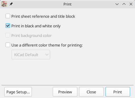
Printing options
Print sheet reference and title block: Include the drawing sheet border and title block in the printed schematic.
Print in black and white only: Print the schematic in black and white rather than color.
Print background color: Include the background color in the printed schematic. This option is only enabled if Print in black and white only is disabled.
Use a different color theme for printing: Select a different color scheme for printing than the one selected for display in the Schematic Editor.
Page Setup…: Opens a page setup dialog for setting paper size and orientation.
Preview: Opens a print preview dialog.
Close: Closes the dialog without printing.
Print: Opens the system print dialog.
| Printing uses platform- and printer-specific drivers and may have unexpected results. When printing to a file, Plotting is recommended instead of Printing. |
Plotting
KiCad can plot schematics to a file using File → Plot….
The supported output formats are Postscript, PDF, SVG, DXF, and HPGL.
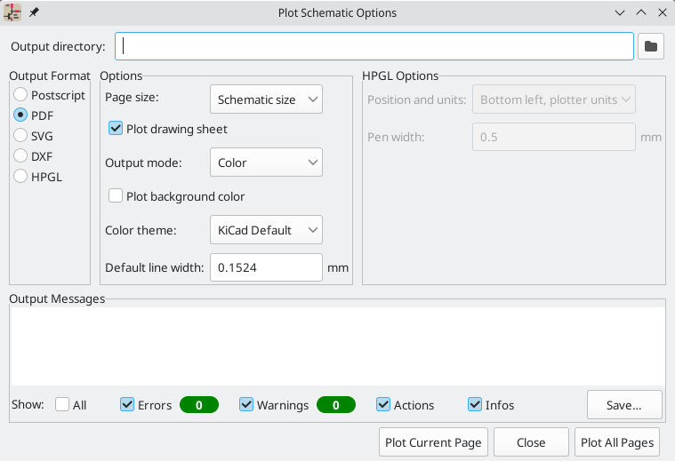
The Output Messages pane displays messages about the generated files. Different kinds of messages can be shown or hidden using the checkboxes, and the messages can be saved to a file using the Save… button.
The Plot Current Page button plots the current page of the schematic. The Plot All Pages button plots all pages of the schematic. One file is generated for each page, except for PDF output, which plots each schematic page as a separate page in a single PDF file.
Plotting options
Output directory: Specify the location to save plotted files. If this is a relative path, it is created relative to the project directory.
Output Format: Select the format to plot in. Some formats have different options than others.
Page size: Sets the page size to use for the plotted output. This can be set to match the schematic size or to another sheet size.
Plot drawing sheet: Include the drawing sheet border and title block in the printed schematic.
Output mode: Sets the output to color or black and white. Not all output formats support color.
Plot background color: Includes the schematic background color in the plotted output. The background color will not be plotted if the output format does not support color or the output mode is black and white.
Color theme: Selects the color theme to use for the plotted output.
Default line width: Selects the default width for lines without a specified thickness (lines that have thickness set to 0). Lines that have a set thickness will be plotted at that thickness instead.
Position and units: Sets the plotter origin and units. This option only applies for HPGL output.
Pen width: Sets the plotter’s pen width. This option only applies for HPGL output.
Generating a Bill of Materials
KiCad can generate a Bill of Materials using Tools → Generate BOM… or the ![]() button on the top toolbar. The generated BOM lists all of the components in the design.
button on the top toolbar. The generated BOM lists all of the components in the design.
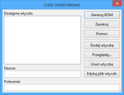
The BOM tool uses an external script to process the design information into the desired output format. Several BOM generator scripts are included with KiCad, and users can also create their own. BOM generator scripts generally use Python or XSLT, but other tools can be used as long as you can specify a command line for KiCad to execute when running the generator.
You can select which BOM generator to use in the BOM generator scripts list. The rest of the dialog displays information about the selected generator. You can change the displayed name of the generator with the Generator nickname textbox.
The pane at right displays information about the selected script. When the generator is executed, the right pane instead displays output from the script.
The text box at the bottom contains the command that KiCad will use to execute the generator. It is automatically populated when a script is selected, but the command may need to be hand-edited for some generators. KiCad saves the command line for each generator when the BOM tool is closed, so command line customizations are preserved. For more details about the command line, see the advanced documentation.
On Windows, the BOM Generator dialog has an additional option Show console window. When this option is unchecked, BOM generators run in a hidden console window and any output is redirected and printed in the dialog. When this option is checked, BOM generators run in a visible console window, which may be necessary if the generator plugin provides a graphical user interface.
BOM generator scripts
By default, the BOM tool presents two output script options.
-
bom_csv_grouped_by_valueoutputs a CSV with two sections. The first section contains every component in the design, with a single component on each line. The second section also contains every component, but components are grouped by symbol name, value, and footprint. The columns in the BOM are:-
Line item number
-
Quantity
-
Reference designator(s)
-
Value
-
Symbol library and symbol name
-
Footprint
-
Datasheet
-
Any other symbol fields
-
-
bom_csv_grouped_by_value_with_fpoutputs a CSV with a single section containing every component in the design. Components are grouped by value and footprint. The columns in the BOM are:-
Reference designator(s)
-
Quantity
-
Value
-
Symbol name
-
Footprint
-
Symbol description
-
Vendor
-
Additional generator scripts are installed with KiCad but are not populated in the generator script list by default. The location of these scripts depends on the operating system and may vary based on installation location.
| Operating System | Location |
|---|---|
Windows |
|
Linux |
|
macOS |
|
Additional scripts can be added to the list of BOM generator scripts by clicking the ![]() button. Scripts can be removed by clicking the
button. Scripts can be removed by clicking the ![]() button. The
button. The ![]() button opens the selected script in a text editor.
button opens the selected script in a text editor.
For more information on creating and using custom BOM generators, see the advanced documentation.
Netlists
A netlist is a file which describes electrical connections between symbol pins. These connections are referred to as nets. Netlist files contain:
-
A list of symbols and their pins.
-
A list of connections (nets) between symbol pins.
Many different netlist formats exist. Sometimes the symbols list and the list of nets are two separate files. This netlist is fundamental in the use of schematic capture software, because the netlist is the link with other electronic CAD software, such as PCB layout software, simulators, and programmable logic compilers.
KiCad supports several netlist formats:
-
KiCad format, which can be imported by the KiCad PCB Editor. However, the "Update PCB from Schematic" tool should be used instead of importing a KiCad netlist into the PCB editor.
-
OrCAD PCB2 format, for designing PCBs with OrCAD.
-
CADSTAR format, for designing PCBs with CADSTAR.
-
Spice format, for use with various external circuit simulators.
| In KiCad version 5.0 and later, it is not necessary to create a netlist for transferring a design from the schematic editor to the PCB editor. Instead, use the "Update PCB from Schematic" tool. |
| Other software tools that use netlists may have restrictions on spaces and special characters in component names, pins, nets, and other fields. For compatibility, be aware of such restrictions in other tools you plan to use, and name components, nets, etc. accordingly. |
Format listy sieci
Netlists are exported with the Export Netlist dialog (File→Export→Netlist…).
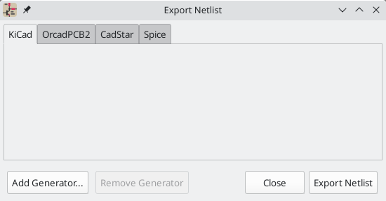
KiCad supports exporting netlists in several formats: KiCad, OrcadPCB2, CADSTAR, and Spice. Each format can be selected by selecting the corresponding tab at the top of the window. Some netlist formats have additional options.
Clicking the Export Netlist button prompts for a netlist filename and saves the netlist.
| Netlist generation can take up to several minutes for large schematics. |
Custom generators for other netlist formats can be added by clicking the Add Generator… button. Custom generators are external tools that are called by KiCad, for example Python scripts or XSLT stylesheets. For more information on custom netlist generators, see the section on adding custom netlist generators.
Spice Netlist Format
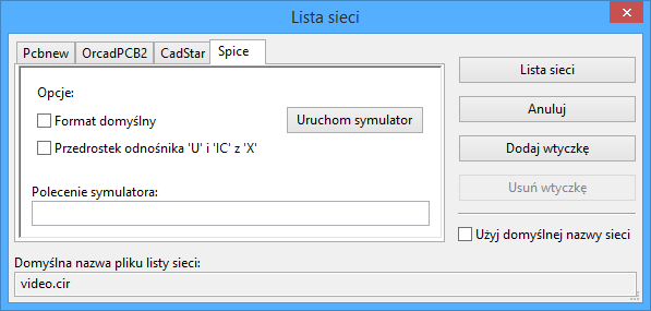
The Spice netlist format offers several options.
When the Reformat passive symbol values box is checked, passive symbol values will be adjusted to be compatible with Spice. Specifically:
-
μandMas unit prefixes are replaced withuandMeg, respectively -
Units are removed (e.g.
4.7kΩis changed to4.7k) -
Values in RKM format are rewritten to be Spice-compatible (e.g.
4u7is changed to4.7u)
The Spice netlist exporter also provides an easy way to simulate the generated netlist with an external simulator. This can be useful for running a simulation without using KiCad’s internal ngspice simulator, or for running an ngspice simulation with options that are not supported by KiCad’s simulator tool.
Enter the path to the external simulator in the text box, with %I representing the generated netlist. Click the Create Netlist and Run Simulator Command button to generate the netlist and automatically run the simulator.
The default simulator command (spice "%I") must be adjusted to point to a simulator installed on your system.
|
Spice simulators expect simulation commands (.PROBE, .AC, .TRAN, etc.) to be included in the netlist. Any text line included in the schematic diagram starting with a period (.) will be included in the netlist. If a text object contains multiple lines, only the lines beginning with a period will be included.
.include directives for including model library files are automatically added to the netlist based on the Spice model settings for the symbols in the schematic.
Przykłady list sieci
Below is the schematic from the sallen_key project included in KiCad’s simulation demos.
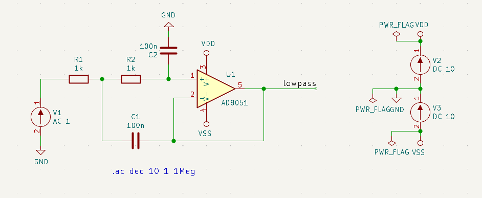
The KiCad format netlist for this schematic is as follows:
(export (version "E")
  (design
    (source "/usr/share/kicad/demos/simulation/sallen_key/sallen_key.kicad_sch")
    (date "Sun 01 May 2022 03:14:05 PM EDT")
    (tool "Eeschema (6.0.4)")
    (sheet (number "1") (name "/") (tstamps "/")
      (title_block
        (title)
        (company)
        (rev)
        (date)
        (source "sallen_key.kicad_sch")
        (comment (number "1") (value ""))
        (comment (number "2") (value ""))
        (comment (number "3") (value ""))
        (comment (number "4") (value ""))
        (comment (number "5") (value ""))
        (comment (number "6") (value ""))
        (comment (number "7") (value ""))
        (comment (number "8") (value ""))
        (comment (number "9") (value "")))))
  (components
    (comp (ref "C1")
      (value "100n")
      (libsource (lib "sallen_key_schlib") (part "C") (description ""))
      (property (name "Sheetname") (value ""))
      (property (name "Sheetfile") (value "sallen_key.kicad_sch"))
      (sheetpath (names "/") (tstamps "/"))
      (tstamps "00000000-0000-0000-0000-00005789077d"))
    (comp (ref "C2")
      (value "100n")
      (fields
        (field (name "Fieldname") "Value")
        (field (name "SpiceMapping") "1 2")
        (field (name "Spice_Primitive") "C"))
      (libsource (lib "sallen_key_schlib") (part "C") (description ""))
      (property (name "Fieldname") (value "Value"))
      (property (name "Spice_Primitive") (value "C"))
      (property (name "SpiceMapping") (value "1 2"))
      (property (name "Sheetname") (value ""))
      (property (name "Sheetfile") (value "sallen_key.kicad_sch"))
      (sheetpath (names "/") (tstamps "/"))
      (tstamps "00000000-0000-0000-0000-00005789085b"))
    (comp (ref "R1")
      (value "1k")
      (fields
        (field (name "Fieldname") "Value")
        (field (name "SpiceMapping") "1 2")
        (field (name "Spice_Primitive") "R"))
      (libsource (lib "sallen_key_schlib") (part "R") (description ""))
      (property (name "Fieldname") (value "Value"))
      (property (name "SpiceMapping") (value "1 2"))
      (property (name "Spice_Primitive") (value "R"))
      (property (name "Sheetname") (value ""))
      (property (name "Sheetfile") (value "sallen_key.kicad_sch"))
      (sheetpath (names "/") (tstamps "/"))
      (tstamps "00000000-0000-0000-0000-0000578906ff"))
    (comp (ref "R2")
      (value "1k")
      (fields
        (field (name "Fieldname") "Value")
        (field (name "SpiceMapping") "1 2")
        (field (name "Spice_Primitive") "R"))
      (libsource (lib "sallen_key_schlib") (part "R") (description ""))
      (property (name "Fieldname") (value "Value"))
      (property (name "SpiceMapping") (value "1 2"))
      (property (name "Spice_Primitive") (value "R"))
      (property (name "Sheetname") (value ""))
      (property (name "Sheetfile") (value "sallen_key.kicad_sch"))
      (sheetpath (names "/") (tstamps "/"))
      (tstamps "00000000-0000-0000-0000-000057890691"))
    (comp (ref "U1")
      (value "AD8051")
      (fields
        (field (name "Spice_Lib_File") "ad8051.lib")
        (field (name "Spice_Model") "AD8051")
        (field (name "Spice_Netlist_Enabled") "Y")
        (field (name "Spice_Primitive") "X"))
      (libsource (lib "sallen_key_schlib") (part "Generic_Opamp") (description ""))
      (property (name "Spice_Primitive") (value "X"))
      (property (name "Spice_Model") (value "AD8051"))
      (property (name "Spice_Lib_File") (value "ad8051.lib"))
      (property (name "Spice_Netlist_Enabled") (value "Y"))
      (property (name "Sheetname") (value ""))
      (property (name "Sheetfile") (value "sallen_key.kicad_sch"))
      (sheetpath (names "/") (tstamps "/"))
      (tstamps "00000000-0000-0000-0000-00005788ff9f"))
    (comp (ref "V1")
      (value "AC 1")
      (libsource (lib "sallen_key_schlib") (part "VSOURCE") (description ""))
      (property (name "Sheetname") (value ""))
      (property (name "Sheetfile") (value "sallen_key.kicad_sch"))
      (sheetpath (names "/") (tstamps "/"))
      (tstamps "00000000-0000-0000-0000-000057336052"))
    (comp (ref "V2")
      (value "DC 10")
      (fields
        (field (name "Fieldname") "Value")
        (field (name "Spice_Node_Sequence") "1 2")
        (field (name "Spice_Primitive") "V"))
      (libsource (lib "sallen_key_schlib") (part "VSOURCE") (description ""))
      (property (name "Fieldname") (value "Value"))
      (property (name "Spice_Primitive") (value "V"))
      (property (name "Spice_Node_Sequence") (value "1 2"))
      (property (name "Sheetname") (value ""))
      (property (name "Sheetfile") (value "sallen_key.kicad_sch"))
      (sheetpath (names "/") (tstamps "/"))
      (tstamps "00000000-0000-0000-0000-0000578900ba"))
    (comp (ref "V3")
      (value "DC 10")
      (fields
        (field (name "Fieldname") "Value")
        (field (name "Spice_Node_Sequence") "1 2")
        (field (name "Spice_Primitive") "V"))
      (libsource (lib "sallen_key_schlib") (part "VSOURCE") (description ""))
      (property (name "Fieldname") (value "Value"))
      (property (name "Spice_Primitive") (value "V"))
      (property (name "Spice_Node_Sequence") (value "1 2"))
      (property (name "Sheetname") (value ""))
      (property (name "Sheetfile") (value "sallen_key.kicad_sch"))
      (sheetpath (names "/") (tstamps "/"))
      (tstamps "00000000-0000-0000-0000-000057890232")))
  (libparts
    (libpart (lib "sallen_key_schlib") (part "C")
      (footprints
        (fp "C?")
        (fp "C_????_*")
        (fp "C_????")
        (fp "SMD*_c")
        (fp "Capacitor*"))
      (fields
        (field (name "Reference") "C")
        (field (name "Value") "C"))
      (pins
        (pin (num "1") (name "") (type "passive"))
        (pin (num "2") (name "") (type "passive"))))
    (libpart (lib "sallen_key_schlib") (part "Generic_Opamp")
      (fields
        (field (name "Reference") "U")
        (field (name "Value") "Generic_Opamp"))
      (pins
        (pin (num "1") (name "+") (type "input"))
        (pin (num "2") (name "-") (type "input"))
        (pin (num "3") (name "V+") (type "power_in"))
        (pin (num "4") (name "V-") (type "power_in"))
        (pin (num "5") (name "") (type "output"))))
    (libpart (lib "sallen_key_schlib") (part "R")
      (footprints
        (fp "R_*")
        (fp "Resistor_*"))
      (fields
        (field (name "Reference") "R")
        (field (name "Value") "R"))
      (pins
        (pin (num "1") (name "") (type "passive"))
        (pin (num "2") (name "") (type "passive"))))
    (libpart (lib "sallen_key_schlib") (part "VSOURCE")
      (fields
        (field (name "Reference") "V")
        (field (name "Value") "VSOURCE")
        (field (name "Fieldname") "Value")
        (field (name "Spice_Primitive") "V")
        (field (name "Spice_Node_Sequence") "1 2"))
      (pins
        (pin (num "1") (name "") (type "input"))
        (pin (num "2") (name "") (type "input")))))
  (libraries
    (library (logical "sallen_key_schlib")
      (uri "/usr/share/kicad/demos/simulation/sallen_key/sallen_key_schlib.kicad_sym")))
  (nets
    (net (code "1") (name "/lowpass")
      (node (ref "C1") (pin "1") (pintype "passive"))
      (node (ref "U1") (pin "2") (pinfunction "-") (pintype "input"))
      (node (ref "U1") (pin "5") (pintype "output")))
    (net (code "2") (name "GND")
      (node (ref "C2") (pin "2") (pintype "passive"))
      (node (ref "V1") (pin "2") (pintype "input"))
      (node (ref "V2") (pin "2") (pintype "input"))
      (node (ref "V3") (pin "1") (pintype "input")))
    (net (code "3") (name "Net-(C1-Pad2)")
      (node (ref "C1") (pin "2") (pintype "passive"))
      (node (ref "R1") (pin "1") (pintype "passive"))
      (node (ref "R2") (pin "2") (pintype "passive")))
    (net (code "4") (name "Net-(C2-Pad1)")
      (node (ref "C2") (pin "1") (pintype "passive"))
      (node (ref "R2") (pin "1") (pintype "passive"))
      (node (ref "U1") (pin "1") (pinfunction "+") (pintype "input")))
    (net (code "5") (name "Net-(R1-Pad2)")
      (node (ref "R1") (pin "2") (pintype "passive"))
      (node (ref "V1") (pin "1") (pintype "input")))
    (net (code "6") (name "VDD")
      (node (ref "U1") (pin "3") (pinfunction "V+") (pintype "power_in"))
      (node (ref "V2") (pin "1") (pintype "input")))
    (net (code "7") (name "VSS")
      (node (ref "U1") (pin "4") (pinfunction "V-") (pintype "power_in"))
      (node (ref "V3") (pin "2") (pintype "input")))))
In Spice format, the netlist is as follows:
.title KiCad schematic
.include "ad8051.lib"
XU1 Net-_C2-Pad1_ /lowpass VDD VSS /lowpass AD8051
C2 Net-_C2-Pad1_ GND 100n
C1 /lowpass Net-_C1-Pad2_ 100n
R2 Net-_C2-Pad1_ Net-_C1-Pad2_ 1k
R1 Net-_C1-Pad2_ Net-_R1-Pad2_ 1k
V1 Net-_R1-Pad2_ GND AC 1
V2 VDD GND DC 10
V3 GND VSS DC 10
.ac dec 10 1 1Meg
.end
Managing Symbol Libraries
Biblioteki symboli przechowują zbiory symboli używanych podczas tworzenia schematów. Każdy symbol na schemacie jest jednoznacznie identyfikowany za pomocą pełnej nazwy, która składa się z nazwy skrótowej biblioteki i nazwy symbolu. Przykładowo Audio:AD1853.
Tabele Bibliotek Symboli
KiCad uses a table of symbol libraries to map symbol libraries to a library nickname. Kicad uses a global symbol library table as well as a table specific to each project. To edit either symbol library table, use Preferences → Manage Symbol Libraries….
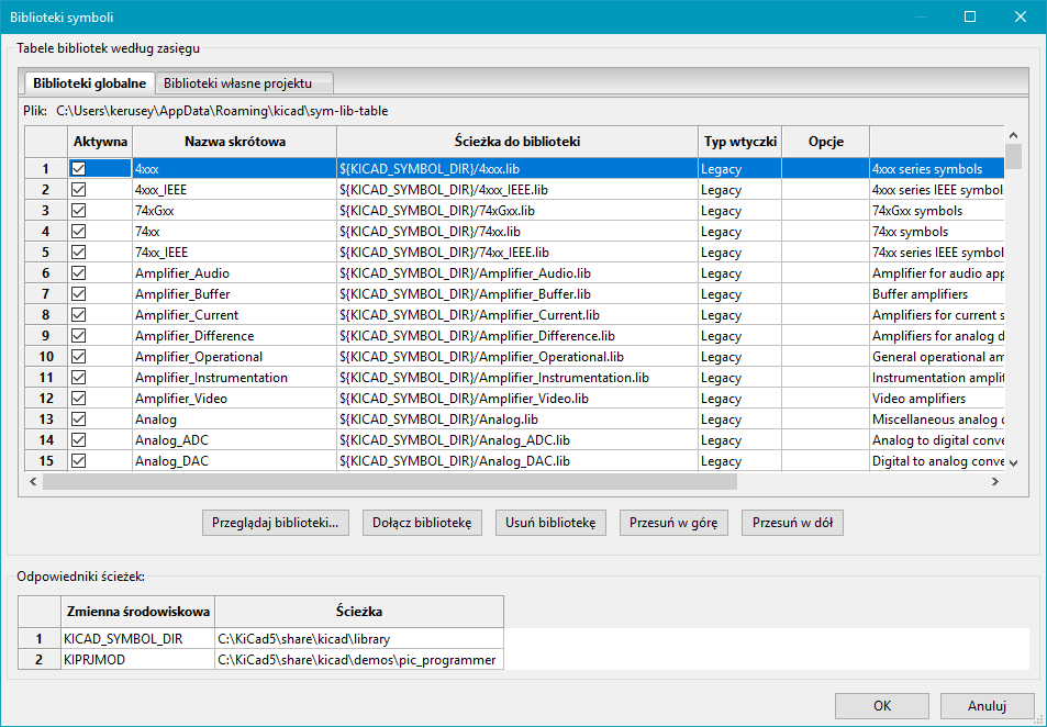
The global symbol library table contains the list of libraries that are always available regardless of the currently loaded project. The table is saved in the file sym-lib-table in the KiCad configuration folder. The location of this folder depends on the operating system being used.
The project specific symbol library table contains the list of libraries that are available specifically for the currently loaded project. If there are any project-specific symbol libraries, the table is saved in the file sym-lib-table in the project folder.
Konfiguracja początkowa
The first time the KiCad Schematic Editor is run and the global symbol table file sym-lib-table is not found in the KiCad configuration folder, KiCad will guide the user through setting up a new symbol library table. This process is described above.
Managing Table Entries
Symbol libraries can only be used if they have been added to either the global or project-specific symbol library table.
Add a library either by clicking the ![]() button and selecting a library or clicking the
button and selecting a library or clicking the ![]() button and typing the path to a library file. The selected library will be added to the currently opened library table (Global or Project Specific). Libraries can be removed by selecting desired library entries and clicking the
button and typing the path to a library file. The selected library will be added to the currently opened library table (Global or Project Specific). Libraries can be removed by selecting desired library entries and clicking the ![]() button.
button.
The ![]() and
and ![]() buttons move the selected library up and down in the library table. This does not affect the display order of libraries in the Symbol Library Browser, Symbol Editor, or Add Symbol tool.
buttons move the selected library up and down in the library table. This does not affect the display order of libraries in the Symbol Library Browser, Symbol Editor, or Add Symbol tool.
Libraries can be made inactive by unchecking the Active checkbox in the first column. Inactive libraries are still in the library table but do not appear in any library browsers and are not loaded from disk, which can reduce loading times.
A range of libraries can be selected by clicking the first library in the range and then Shift-clicking the last library in the range.
Each library must have a unique nickname: duplicate library nicknames are not allowed in the same table. However, nicknames can be duplicated between the global and project library tables. Libraries in the project table take precedence over libraries with the same name in the global table.
Library nicknames do not have to be related to the library filename or path. The colon character (:) cannot be used in library nicknames or symbol names because it is used as a separator between nicknames and symbols.
Each library entry must have a valid path. Paths can be defined as absolute, relative, or by environment variable substitution.
The appropriate library format must be selected in order for the library to be properly read. "KiCad" format is used for KiCad version 6 libraries (.kicad_sym files), while "Legacy" format is used for libraries from older versions of KiCad (.lib files). Legacy libraries are read-only, but can be migrated to KiCad format libraries using the Migrate Libraries button (see section Migrating Legacy Libraries).
There is an optional description field to add a description of the library entry. The option field is not used at this time so adding options will have no effect when loading libraries.
Substytucja zmiennych środowiskowych
The symbol library tables support environment variable substitution, which allows you to define environment variables containing custom paths to where your libraries are stored. Environment variable substitution is supported by using the syntax ${ENV_VAR_NAME} in the symbol library path.
By default, KiCad defines several environment variables:
-
${KIPROJMOD}points to the current project directory and cannot be modified. -
${KICAD6_FOOTPRINT_DIR}points to the default location of KiCad’s standard footprint libraries. -
${KICAD6_SYMBOL_DIR}points to the default location of KiCad’s standard symbol libraries. -
${KICAD6_3DMODEL_DIR}points to the default location of KiCad’s standard 3D model libraries. -
${KICAD6_TEMPLATE_DIR}points to the default location of KiCad’s standard template library.
${KIPROJMOD} cannot be redefined, but the other environment variables can be redefined and new environment variables added in the Preferences → Configure Paths… dialog.
Using environment variables in the symbol library tables allows libraries to be relocated without breaking the symbol library tables, so long as the environment variables are updated when the library location changes.
${KIPROJMOD} allows libraries to be stored in the project folder without having to use an absolute path in the project library table. This makes it possible to relocate projects without breaking their project library tables. One of the most powerful features of the symbol library table is environment variable substitution. This allows for definition of custom paths to where symbol libraries are stored in environment variables. Environment variable substitution is supported by using the syntax ${ENV_VAR_NAME} in the library path.
Zakres stosowania
Symbol libraries can be defined either globally or specifically to the currently loaded project. Symbol libraries defined in the user’s global table are always available and are stored in the sym-lib-table file in the user’s KiCad configuration folder. The project-specific symbol library table is active only for the currently open project file.
Każda z tych metod ma swoje wady i zalety. Zdefiniowanie wszystkich bibliotek w tabeli globalnej oznacza, że będą one zawsze dostępne w razie potrzeby. Wadą tego rozwiązania jest to, że czas ich ładowania znacznie wzrośnie.
Definiowanie wszystkich bibliotek symboli w ustawieniach konkretnego projektu oznacza, że ładowane są tylko biblioteki wymagane dla projektu co zmniejsza ich czas ładowania. Wadą jest to, że zawsze należy pamiętać o skonfigurowaniu wymaganych bibliotek dla każdego projektu.
Jednym ze sposobów użycia mogłoby być zdefiniowanie powszechnie używanych bibliotek globalnie, a bibliotek wymaganych tylko dla projektu w tabelach bibliotek specyficznych dla projektu. Nie pod tym względem żadnych ograniczeń.
Migrating Legacy Libraries
Legacy libraries (.lib files) are read-only, but they can be migrated to KiCad version 6 libraries (.kicad_sym). KiCad version 6 libraries cannot be viewed or edited by KiCad versions older than 6.0.0.
Legacy libraries can be converted to KiCad 6 libraries by selecting them in the symbol library table and clicking the Migrate Libraries button. Multiple libraries can be selected and migrated at once by Ctrl-clicking or shift-clicking.
Libraries can also be converted one at a time by opening them in the Symbol Editor and saving them as a new library.
Remapowanie projektów z poprzednich wersji
When loading a schematic created prior to the symbol library table implementation, KiCad will attempt to remap the symbol library links in the schematic to the appropriate library table symbols. The success of this process is dependent on several factors:
-
oryginalne biblioteki użyte w schemacie są nadal dostępne i niezmienione od momentu dodania symbolu do schematu.
-
wszystkie operacje ratunkowe zostały wykonane po wykryciu potrzeby utworzenia biblioteki ratunkowej lub aktualizacji istniejącej biblioteki ratunkowej.
-
integralność symboli bibliotecznych w pamięci podręcznej projektu nie została naruszona.
|
Remapowanie spowoduje utworzenie kopii zapasowej wszystkich plików, które zostały zmienione podczas ponownego mapowania w folderze |
|
Operacja odzyskiwania jest wykonywana nawet jeśli została wyłączona, aby zabezpieczyć poprawność symboli do procesu ponownego mapowania. Nie powinno się anulować tej operacji, inaczej ponowne mapowanie się nie powiedzie. Wszelkie uszkodzone łącza symboliczne muszą wtedy zostać naprawione ręcznie. |
|
If the original libraries have been removed and the rescue was not performed, the cache library can be used as a recovery library as a last resort. Copy the cache library to a new file name and add the new library file to the top of the library list using a version of KiCad prior to the symbol library table implementation. |
Symbol Editor
Podstawowe informacje na temat bibliotek
A symbol is a schematic element which contains a graphical representation, electrical connections, and text fields describing the symbol. Symbols used in a schematic are stored in symbol libraries. KiCad provides a symbol editing tool that allows you to create libraries, add, delete or transfer symbols between libraries, export symbols to files, and import symbols from files. The symbol editing tool provides a simple way to manage symbols and symbol libraries.
Biblioteki symboli - Przegląd
Biblioteka symboli składa się z jednego bądź wielu komponentów. Generalnie, komponenty są logicznie pogrupowane biorąc pod uwagę np. ich funkcję, typ, bądź producenta.
Symbol znajdujący się w bibliotece jest złożony z:
-
Graphical items (lines, circles, arcs, text, etc.) that determine how symbol looks in a schematic.
-
Pins which have both graphic properties (line, clock, inverted, low level active, etc.) and electrical properties (input, output, bidirectional, etc.) used by the Electrical Rules Check (ERC) tool.
-
Pól (tekstowych) takich jak oznaczenie, wartość, nazwa footprintu potrzebna do wstawienia go na płytkę.
Symbols can be derived from another symbol in the same library. Derived symbols share the base symbol’s graphical shape and pin definitions, but can override the base symbol’s property fields (value, footprint, footprint filters, datasheet, description, etc.). Derived symbols can be used to define symbols that are similar to a base part. For example, 74LS00, 74HC00, and 7437 symbols could all be derived from a 7400 symbol. In previous versions of KiCad, derived symbols were referred to as aliases.
Do poprawnego tworzenia symboli wymagane jest:
-
Zdefiniowanie ogólnych właściwości: czy posiada wiele części składowych.
-
Defining if the symbol has an alternate body style (also known as a De Morgan representation).
-
Projektowanie wyglądu (z wyjątkiem pinów) z użyciem linii, prostokątów, okręgów, wielokątów i tekstów.
-
Dodanie wyprowadzeń, dokładnie określając ich projekt graficzny, nazwę oraz numer pinu, a także ich właściwości elektryczne (wejście, wyjście, trzy-stanowe, port zasilania, itp.).
-
Determining if the symbol should be derived from another symbol with the same graphical design and pin definition.
-
Dodanie pól w razie potrzeby (jest to opcjonalne, nazwa modułu jest wykorzystywany przez oprogramowanie PCB) i/lub określenie ich widoczności.
-
Dokumentowanie składnika np. poprzez dodanie słów kluczowych i adresu dokumentacji w sieci lub na lokalnym nośniku.
-
Zapisanie go do wybranej biblioteki.
Edytor bibliotek symboli - Przegląd
Widok głównego okna edytora bibliotek symboli znajduje się poniżej. Edytor składa się z trzech pasków narzędzi z szybkim dostępem do podstawowych narzędzi i obszaru podglądu/edycji komponentów. Nie wszystkie polecenia są dostępne na paskach narzędzi, ale można uzyskać do nich dostęp za pomocą menu.
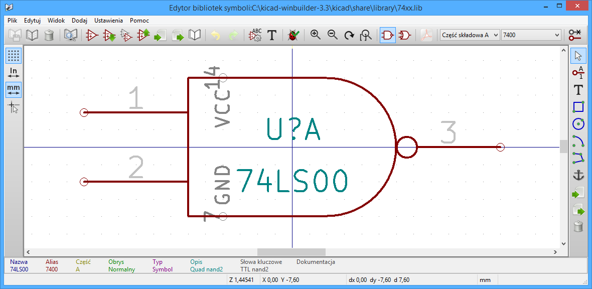
Główny pasek menu
The main tool bar is located at the top of the main window. It consists of the undo/redo commands, zoom commands, symbol properties dialogs, and unit/representation management controls.

|
Create a new symbol in the selected library. |
|
Save the currently selected library. All modified symbols in the library will be saved. |
|
Undo last edit. |
|
Redo last undo. |
|
Refresh display. |
|
Zoom in. |
|
Zoom out. |
|
Zoom to fit symbol in display. |
|
Zoom to fit selection. |
|
Rotate counter-clockwise. |
|
Rotate clockwise. |
|
Mirror horizontally. |
|
Mirror vertically. |
|
Edit the current symbol properties. |
|
Edit the symbol’s pins in a tablular interface. |
|
Open the symbol’s datasheet. The button will be disabled if no datasheet is defined for the current symbol. |
|
Test the current symbol for design errors. |
|
Select the normal body style. The button is disabled if the current symbol does not have an alternate body style. |
|
Select the alternate body style. The button is disabled if the current symbol does not have an alternate body style. |
|
Select the unit to display. The drop down control will be disabled if the current symbol is not derived from a symbol with multiple units. |
|
Enable synchronized pins edit mode. When this mode is enabled, any pin modifications are propagated to all other symbol units. Pin number changes are not propagated. This mode is automatically enabled for symbols with multiple interchangeable units and cannot be enabled for symbols with only one unit. |
|
Insert current symbol into schematic. |
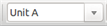
Pasek narzędzi edycji symbolu
The vertical toolbar located on the right hand side of the main window allows you to place all of the elements required to design a symbol.
|
Select tool. Right-clicking with the select tool opens the context menu for the object under the cursor. Left-clicking with the select tool displays the attributes of the object under the cursor in the message panel at the bottom of the main window. Double-left-clicking with the select tool will open the properties dialog for the object under the cursor. |
|
Pin tool. Left-click to add a new pin. |
|
Graphical text tool. Left-click to add a new graphical text item. |
|
Rectangle tool. Left-click to begin drawing the first corner of a graphical rectangle. Left-click again to place the opposite corner of the rectangle. |
|
Circle tool. Left-click to begin drawing a new graphical circle from the center. Left-click again to define the radius of the circle. |
|
Arc tool. Left-click to begin drawing a new graphical arc item from the first arc end point. Left-click again to define the second arc end point. Adjust the radius by dragging the arc center point. |
|
Connected line tool. Left-click to begin drawing a new graphical line item in the current symbol. Left-click for each additional connected line. Double-left-click to complete the line. |
|
Anchor tool. Left-click to set the anchor position of the symbol. |
|
Delete tool. Left-click to delete an object from the current symbol. |
Pasek opcji
The vertical tool bar located on the left hand side of the main window allows you to set some of the editor drawing options.
|
Toggle grid visibility on and off. |
|
Set units to inches. |
|
Set units to mils (0.001 inch). |
|
Set units to millimeters. |
|
Toggle full screen cursor on and off. |
|
Toggle display of pin electrical types. |
|
Toggle display of libraries and symbols. |
Wybór bibliotek i zarządzanie nimi
The selection of the current library is possible via the ![]() icon which shows you all available libraries and allows you to select one. When a symbol is loaded or saved, it will be put in this library. The library name of a symbol is the contents of its
icon which shows you all available libraries and allows you to select one. When a symbol is loaded or saved, it will be put in this library. The library name of a symbol is the contents of its Value field.
Wybór i zapis symbolu
Wybór symbolu
Clicking the ![]() icon on the left tool bar toggles the treeview of libraries and symbols. Clicking on a symbol opens that symbol.
icon on the left tool bar toggles the treeview of libraries and symbols. Clicking on a symbol opens that symbol.
| Some symbols are derived from other symbols. Derived symbol names are displayed in italics in the treeview. If a derived symbol is opened, its symbol graphics will not be editable. Its symbol fields will be editable as normal. To edit the graphics of a base symbol and all of its derived symbols, open the base symbol. |
Zapisywanie symbolu
After modification, a symbol can be saved in the current library or a different library.
To save the modified symbol in the current library, click the ![]() icon. The modifications will be written to the existing symbol.
icon. The modifications will be written to the existing symbol.
| Saving a modified symbol also saves all other modified symbols in the same library. |
To save the symbol changes to a new symbol, click File → Save As…. The symbol can be saved in the current library or a different library. A new name can be set for the symbol.
To create a new file containing only the current symbol, click File → Export → Symbol…. This file will be a standard library file which will contain only one symbol.
Tworzenie symboli biblliotecznych
Tworzenie nowego symbolu
A new symbol can be created by clicking the ![]() icon. You will be asked for a number of symbol properties.
icon. You will be asked for a number of symbol properties.
-
A symbol name (this name is used as the default value for the
Valuefield in the schematic editor) -
An optional base symbol to derive the new symbol from. The new symbol will use the base symbol’s graphical shape and pin configuration, but other symbol information can be modified in the derived symbol. The base symbol must be in the same library as the new derived symbol.
-
The reference designator prefix (
U,C,R…). -
The number of units per package, and whether those units are interchangeable (for example a 7400 is made of 4 units per package).
-
If an alternate body style (sometimes referred to as a "De Morgan equivalent") is desired.
-
Whether the symbol is a power symbol. Power symbols appear in the "Add Power Port" dialog in the Schematic editor, their
Valuefields are not editable in the schematic, they cannot be assigned a footprint and they are not added to the PCB, and they are not included in the bill of materials. -
Whether the symbol should be excluded from the bill of materials.
-
Whether the symbol should be excluded from the PCB.
There are also several graphical options.
-
The offset between the end of each pin and its pin name.
-
Whether the pin number and pin name should be displayed.
-
Whether the pin names should be displayed alongside the pins or at the ends of the pins inside the symbol body.
These properties can also be changed later in the Symbol Properties window.
Nowy symbol będzie utworzony z użyciem powyższych właściwości i pojawi się w oknie edycyjnym jak pokazano poniżej.
The blue cross in the center is the symbol anchor, which specifies the symbol origin i.e. the coordinates (0, 0). The anchor can be repositioned by selecting the ![]() icon and clicking on the new desired anchor position.
icon and clicking on the new desired anchor position.
Tworzenie nowego symbolu na podstawie innego
Często symbol który chcemy utworzyć bardzo przypomina inny symbol, który znajduje się już w bibliotece. W tym przypadku łatwiej jest zmodyfikować istniejący symbol.
-
Załadować symbol który będzie użyty jako wzorcowy.
-
Save a new copy of the symbol using File → Save As…. The Save As dialog will prompt for a name for the new symbol and the library to save it in.
-
Wykonać niezbędne edycje.
-
Save the modified symbol.
Właściwości symbolu
Symbol properties are set when the symbol is created but they can be modified at any point. To change the symbol properties, click on the ![]() icon to show the dialog below.
icon to show the dialog below.
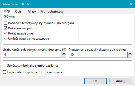
It is important to correctly set the number of units per package and the alternate symbolic representation, if enabled, because when pins are edited or created the corresponding pins for each unit will be affected. If you change the number of units per package after pin creation and editing, there will be additional work to specify the pins and graphics for the new unit. Nevertheless, it is possible to modify these properties at any time.
The graphic options "Show pin number" and "Show pin name" define the visibility of the pin number and pin name text. The option "Place pin names inside" defines the pin name position relative to the pin body. The pin names will be displayed inside the symbol outline if the option is checked. In this case the "Pin Name Position Offset" property defines the shift of the text away from the body end of the pin. A value from 0.02 to 0.05 inches is usually reasonable.
Poniższy przykład pokazuje symbol, w którym opcja "Umieść nazwę pinu wewnątrz" została odznaczona. Należy zwrócić uwagę na położenie nazw i numerów pinów.
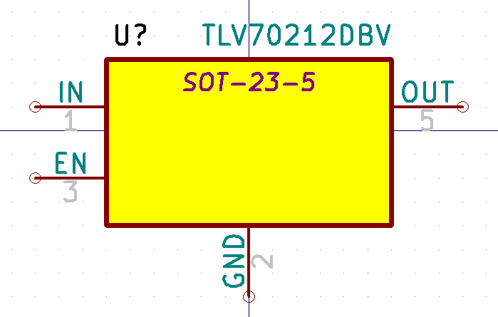
Symbol Name, Description, and Keywords
The symbol’s name is the same as the Value field. When the symbol name is changed the value also changes, and vice versa. The symbol’s name in the library also changes accordingly.
The symbol description should contain a brief description of the component, such as the component function, distinguishing features, and package options. The keywords should contain additional terms related to the component. Keywords are used primarily to assist in searching for the symbol.
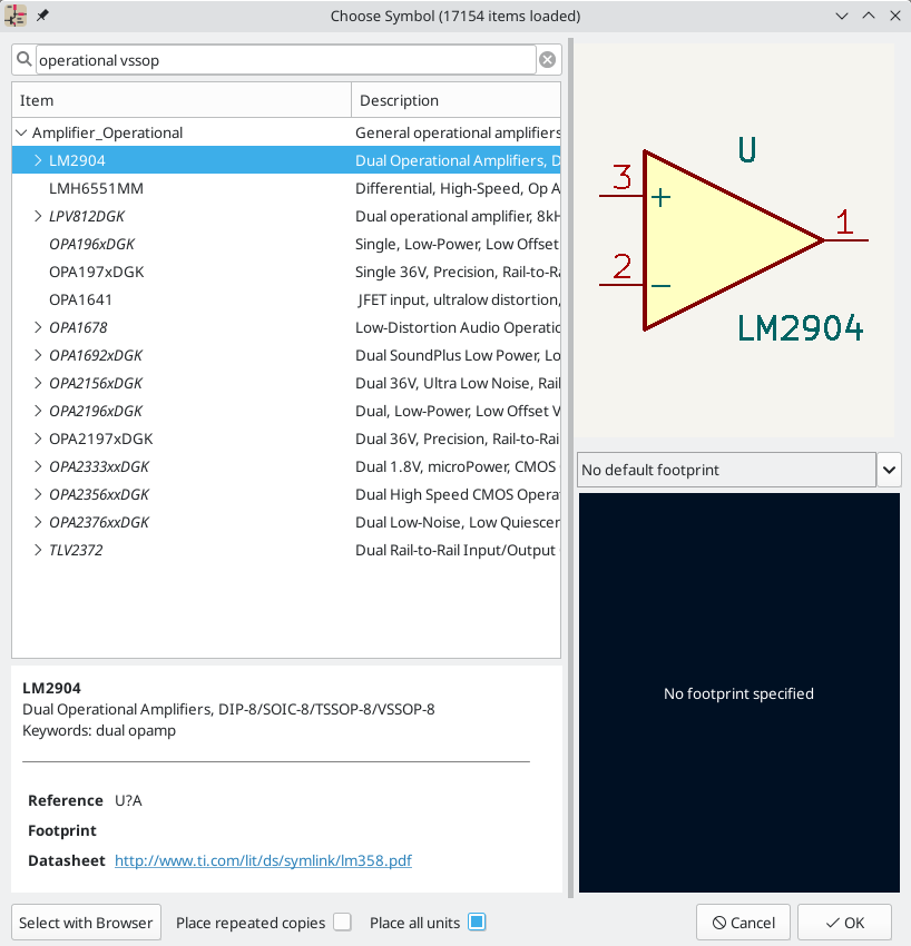
A symbol’s name, description, and keywords are all used when searching for symbols in the Symbol Editor and Add a Symbol dialog. The description and keywords are displayed in the Symbol Library Browser and Add a Symbol dialog.
Footprint Filters
The footprint filters tab is used to define which footprints are appropriate to use with the symbol. The filters can be applied in the Footprint Assignment tool so that only appropriate footprints are displayed for each symbol.
Multiple footprint filters can be defined. Footprints that match any of the filters will be displayed; if no filters are defined, then all footprints will be displayed.
Filters can use wildcards: * matches any number of characters, including zero, and ? matches zero or one characters. For example, SOIC-* would match the SOIC-8_3.9x4.9mm_P1.27mm footprint as well as any other footprint beginning with SOIC-. The filter SOT?23 matches SOT23 as well as SOT-23.
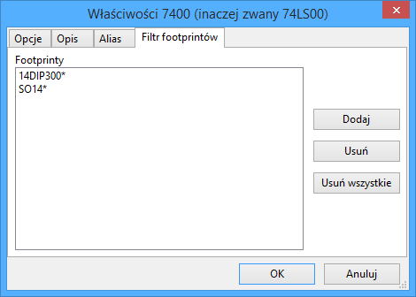
Symbole wieloczęściowe i podwójna reprezentacja
If the symbol has an alternate body style defined, one body style must be selected for editing at a time. To edit the normal representation, click the ![]() icon.
icon.
To edit the alternate representation, click on the ![]() icon. Use the
icon. Use the 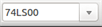 dropdown shown below to select the unit you wish to edit.
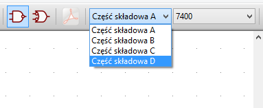
Elementy graficzne symbolu
Graphical elements create the visual representation of a symbol and contain no electrical connection information. Graphical elements are created with the following tools:
-
Linie i linie łamane są definiowane poprzez punkty startowe i końcowe.
-
Prostokąty są definiowane przez punkty dwóch przeciwległych narożników.
-
Okręgi są definiowane przez punkt centralny i promień.
-
Łuki są definiowane przez punkt początkowy i końcowy łuku oraz ich punkt centralny. Kąt rozwarcia łuku może zawierać się w przedziale 0° to 180°.
Pasek narzędzi po prawej stronie głównego okna pozwala na umieszczanie w polu roboczym wszystkich podstawowych elementów graficznych potrzebnych do zaprojektowania symbolu w obu jego postaciach.
Przynależność elementów graficznych
Każdy z elementów graficznych (linia, łuk, okrąg, itd.) może być określona jako część wspólna dla wszystkich części składowych lub stylów, albo specyficzna dla nich. Opcje dotyczące przynależności elementu graficznego można łatwo wyświetlić klikając prawym klawiszem myszy nad wybranym elementem wywołując menu podręczne. Poniżej przykład menu dla elementu typu linia.
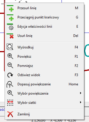
Można także kliknąć dwukrotnie na taki element by zmodyfikować jego właściwości. Poniżej przykład dla elementu typu linia łamana.
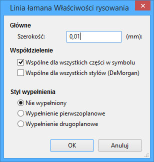
Głównymi właściwościami dla elementów graficznych są:
-
"Line width" defines the width of the element’s line in the current drawing units.
-
"Fill Style" determines if the shape defined by the graphical element is to be drawn unfilled, background filled, or foreground filled.
-
"Common to all units in symbol" determines if the graphical element is drawn for each unit in symbol with more than one unit per package or if the graphical element is only drawn for the current unit.
-
"Common to all body styles (De Morgan)" determines if the graphical element is drawn for each symbolic representation in symbols with an alternate body style or if the graphical element is only drawn for the current body style.
Tekst jako grafika w symbolu
The ![]() icon allows for the creation of graphical text. Graphical text is automatically oriented to be readable, even when the symbol is mirrored. Please note that graphical text items are not the same as symbol fields.
icon allows for the creation of graphical text. Graphical text is automatically oriented to be readable, even when the symbol is mirrored. Please note that graphical text items are not the same as symbol fields.
Symbole wieloczęściowe, podwójna reprezentacja symboli
Symbols can have up to two body styles (a standard symbol and an alternate symbol often referred to as a "De Morgan equivalent") and/or have more than one unit per package (logic gates for example). Some symbols can have more than one unit per package each with different symbols and pin configurations.
Consider for instance a relay with two switches, which can be designed as a symbol with three different units: a coil, switch 1, and switch 2. Designing a symbol with multiple units per package and/or alternate body styles is very flexible. A pin or a body symbol item can be common to all units or specific to a given unit or they can be common to both symbolic representation so are specific to a given symbol representation.
By default, pins are specific to a unit and body style. When a pin is common to all units or all body styles, it only needs to be created once. This is also the case for the body style graphic shapes and text, which may be common to each unit, but typically are specific to each body style).
Example of a Symbol With Multiple Noninterchangeable Units
For an example of a symbol with multiple units that are not interchangeable, consider a relay with 3 units per package: a coil, switch 1, and switch 2.
The three units are not all the same, so "All units are interchangeable" should be deselected in the Symbol Properties dialog. Alternatively, this option could have been specified when the symbol was initially created.
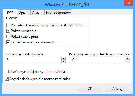
Unit A
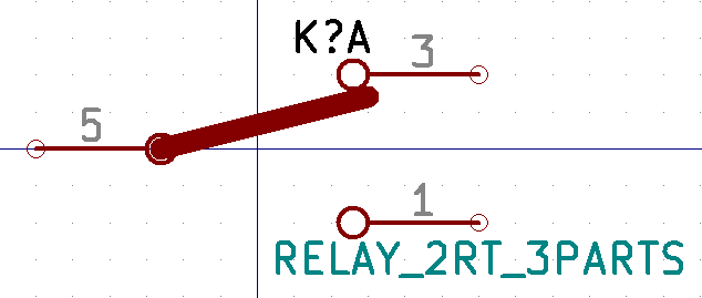
Unit B
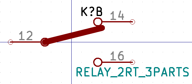
Unit C
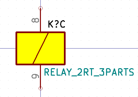
Unit A does not have the same symbol and pin layout as Units B and C, so the units are not interchangeable.
|
"Synchronized Pins Edit Mode" can be enabled by clicking the |
Elementy geometryczne w symbolach
Shown below are properties for a graphic body element. In the relay example above, the three units have different symbolic representations. Therefore, each unit was created separately and the graphical body elements have the "Common to all units in symbol" setting disabled.
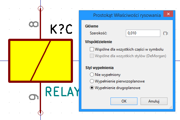
Tworzenie i edycja wyprowadzeń (pinów)
You can click on the ![]() icon to create and insert a pin. The editing of all pin properties is done by double-clicking on the pin or right-clicking on the pin to open the pin context menu. Pins must be created carefully, because any error will have consequences on the PCB design. Any pin already placed can be edited, deleted, and/or moved.
icon to create and insert a pin. The editing of all pin properties is done by double-clicking on the pin or right-clicking on the pin to open the pin context menu. Pins must be created carefully, because any error will have consequences on the PCB design. Any pin already placed can be edited, deleted, and/or moved.
Wyprowadzenia - Informacje podstawowe
A pin is defined by its graphical representation, its name and its number. The pin’s name and number can contain letters, numbers, and symbols, but not spaces. For the Electrical Rules Check (ERC) tool to be useful, the pin’s electrical type (input, output, tri-state…) must also be defined correctly. If this type is not defined properly, the schematic ERC check results may be invalid.
Ważne uwagi:
-
Symbol pins are matched to footprint pads by number. The pin number in the symbol must match the corresponding pad number in the footprint.
-
Do not use spaces in pin names and numbers. Spaces will be automatically replaced with underscores (
_). -
To define a pin name with an inverted signal (overline) use the
~(tilde) character followed by the text to invert in braces. For example~{FO}Owould display FO O. -
If the pin name is empty, the pin is considered unnamed.
-
Pin names can be repeated in a symbol.
-
Pin numbers must be unique in a symbol.
Właściwości wyprowadzeń
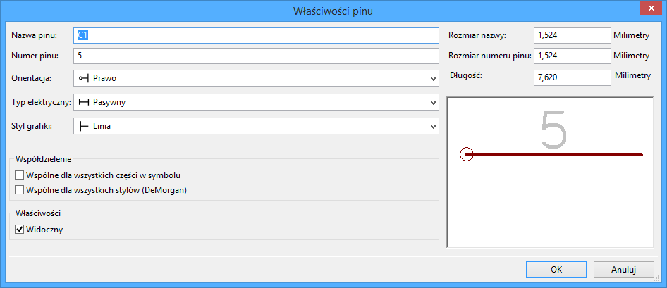
Okno z właściwościami pinu pozwala na zmiany charakterystycznych cech wyprowadzeń. Okno to ukazuje się zawsze podczas tworzenia nowego pinu, albo gdy w pin zostanie kliknięty dwukrotnie myszą. Jego zawartość pozwala na zdefiniowanie lub modyfikację parametrów takich jak:
-
The pin name and text size.
-
The pin number and text size.
-
The pin length.
-
The pin electrical type and graphical style.
-
Przynależność do części i alternatywnej reprezentacji.
-
Pin visibility.
Pin Graphic Styles
Shown in the figure below are the different pin graphic styles. The choice of graphic style does not have any influence on the pin’s electrical type.
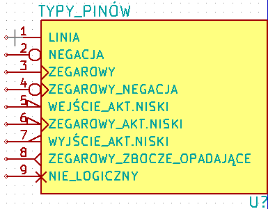
Typy elektryczne
Choosing the correct electrical type is important for the schematic ERC tool. ERC will check that pins are connected appropriately, for example ensuring that input pins are driven and power inputs receive power from an appropriate source.
Pin Type |
Description |
Input |
A pin which is exclusively an input. |
Output |
A pin which is exclusively an output. |
Bidirectional |
A pin that can be either an input or an output, such as a microcontroller data bus pin. |
Tri-state |
A three state output pin (high, low, or high impedance) |
Passive |
A passive symbol pin: resistors, connectors, etc. |
Free |
A pin that can be freely connected to any other pin without electrical concerns. |
Unspecified |
A pin for which the ERC check does not matter. |
Power input |
A symbol’s power pin. As a special case, power input pins that are marked invisible are automatically connected to the net with the same name. See the Power Ports section for more information. |
Power output |
A pin that provides power to other pins, such as a regulator output. |
Open collector |
An open collector logic output. |
Open emitter |
An open emitter logic output. |
Unconnected |
A pin that should not be connected to anything. |
Pushing Pin Properties to Other Pins
You can apply the length, name size, or number size of a pin to the other pins in the symbol by right clicking the pin and selecting Push Pin Length, Push Pin Name Size, or Push Pin Number Size, respectively.
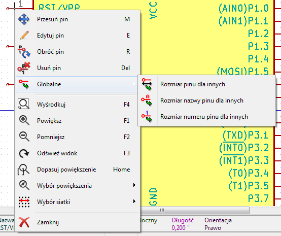
Określanie pinów w symbolach wieloczęściowych i podwójna reprezentacja
Symbols with multiple units and/or graphical representations are particularly problematic when creating and editing pins. The majority of pins are specific to each symbol unit (because each unit has a different set of pins) and to each body style (because the form and position is different between the normal body style and the alternate form).
The symbol library editor allows the simultaneous creation of pins. By default, changes made to a pin are made for all units of a multiple unit symbol and to both representations for symbols with an alternate symbolic representation. The only exception to this is the pin’s graphical type and name, which remain unlinked between symbol units and body styles. This dependency was established to allow for easier pin creation and editing in most cases. This dependency can be disabled by toggling the ![]() icon on the main tool bar. This will allow you to create pins for each unit and representation completely independently.
icon on the main tool bar. This will allow you to create pins for each unit and representation completely independently.
Pins can be common or specific to different units. Pins can also be common to both symbolic representations or specific to each symbolic representation. When a pin is common to all units, it only has to drawn once. Pins are set as common or specific in the pin properties dialog.
An example is the output pin in the 7400 quad dual input NAND gate. Since there are four units and two symbolic representations, there are eight separate output pins defined in the symbol definition. When creating a new 7400 symbol, unit A of the normal symbolic representation will be shown in the library editor. To edit the pin style in the alternate symbolic representation, it must first be enabled by clicking the ![]() button on the tool bar. To edit the pin number for each unit, select the appropriate unit using the drop down control.
button on the tool bar. To edit the pin number for each unit, select the appropriate unit using the drop down control.
Pin Table
Another way to edit pins is to use the Pin Table, which is accessible via the ![]() icon. The Pin Table displays all of the pins in the symbol and their properties in a table view, so it is useful for making bulk pin changes.
icon. The Pin Table displays all of the pins in the symbol and their properties in a table view, so it is useful for making bulk pin changes.
Any pin property can be edited by clicking on the appropriate cell. Pins can be added and removed with the ![]() and
and ![]() icons, respectively.
icons, respectively.
| Columns of the pin table can be shown or hidden by right-clicking on the header row and checking or unchecking additional columns. Some columns are hidden by default. |
The screenshot below shows the pin table for a quad opamp.
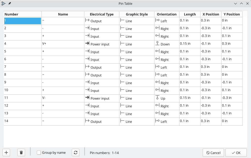
Alternate Pin Definitions
Pins can have alternate pin definitions added to them. Alternate pin definitions allow a user to select a different name, electrical type, and graphical style for a pin when the symbol has been placed in the schematic. This can be used for pins that have multiple functions, such as microcontroller pins.
Alternate pin definitions are added in the Pin Properties dialog as shown below. Each alternate definition contains a pin name, electrical type, and graphic style. This microcontroller pin has all of its peripheral functions defined in the symbol as alternate pin names.
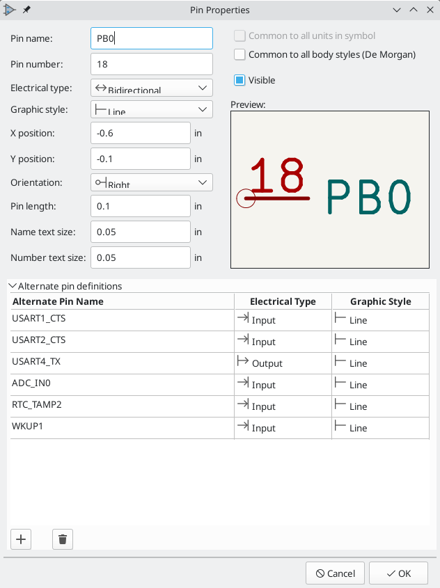
Alternate pin definitions are selected in the Schematic Editor once the symbol has been placed in the schematic. The alternate pin is assigned in the Alternate Pin Assignments tab of the Symbol Properties dialog. Alternate definitions are selectable in the dropdown in the Alternate Assignment column.
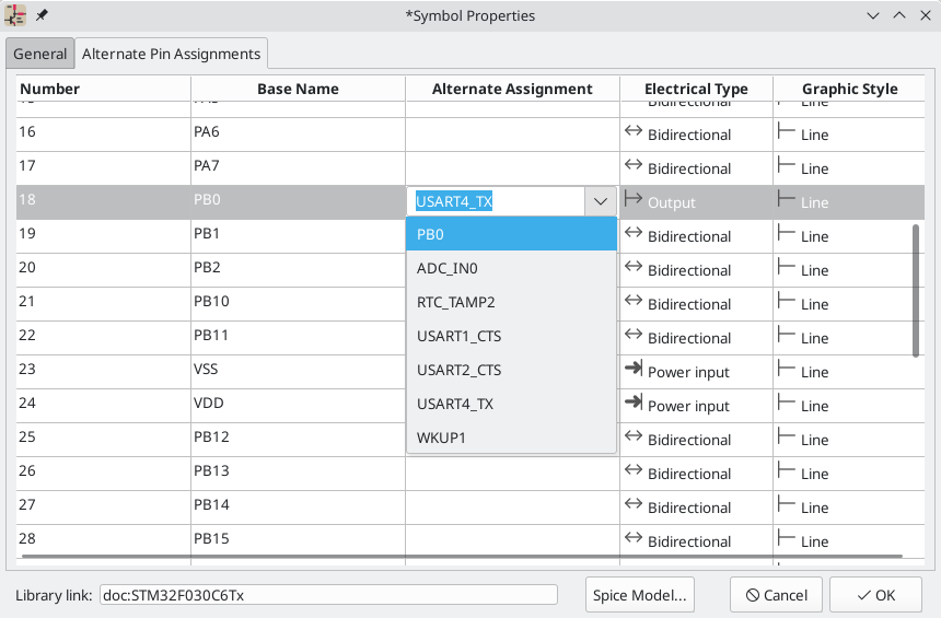
Pola symboli
All library symbols are defined with four default fields. The reference designator, value, footprint assignment, and datasheet link fields are created whenever a symbol is created or copied. Only the reference designator and value fields are required.
Symbols defined in libraries are typically defined with only these four default fields. Additional fields such as vendor, part number, unit cost, etc. can be added to library symbols but generally this is done in the schematic editor so the additional fields can be applied to all of the symbols in the schematic.
| A convenient way to create additional empty symbol fields is to use define field name templates. Field name templates define empty fields that are added to each symbol when it is inserted into the schematic. Field name templates can be defined globally (for all schematics) in the Schematic Editor Preferences, or they can be defined locally (specific to each project) in the Schematic Setup dialog. |
Edycja pól symboli
By dokonać edycji istniejącego pola symbolu, należy kliknąć prawym klawiszem na polu tekstowym by wywołać menu kontekstowe pokazane poniżej.
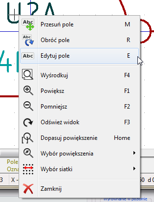
To add new fields, delete optional fields, or edit existing fields, use the ![]() icon on the main tool bar to open the Symbol Properties dialog.
icon on the main tool bar to open the Symbol Properties dialog.
Fields are text information associated a the symbol. Do not confuse them with text in the graphic representation of a symbol.
Ważne uwagi:
-
Modifying the
Valuefield changes the name of the symbol. The symbol’s name in the library will change when the symbol is saved. -
The Symbol Properties dialog must be used to edit a field that is empty or has the invisible attribute enabled because such fields cannot be clicked on.
-
The footprint is defined as an absolute footprint using the
LIBNAME:FOOTPRINTNAMEformat whereLIBNAMEis the name of the footprint library defined in the footprint library table (see the "Footprint Library Table" section in the PCB Editor manual) andFOOTPRINTNAMEis the name of the footprint in the libraryLIBNAME.
Creating Power Port Symbols
Power ports, or power symbols, are symbols that are used to label a wire as part of a power net, like VCC or GND. The behavior of power ports is described in the electrical connections section. Power symbols are handled and created the same way as normal symbols, but there are several additional considerations described below.
It may be useful to place power symbols in a dedicated library. KiCad’s symbol library places power symbols in the power library, and users may create libraries to store their own power symbols. If the "Define as power symbol" box is checked in a symbol’s properties, that symbol will appear in the Schematic Editor’s "Add Power Port" dialog for convenient access.
Below is an example of a GND power symbol.
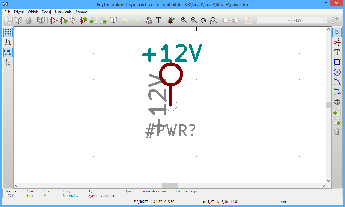
Power port symbols consist of a pin of type "Power input" that is marked invisible. They must also have the "Define as power symbol" property checked. Invisible power input pins have a special property of making implicit global connections based on the pin name.
| If the power symbol has the "Define as power symbol" property checked, the power input pin does not need to be marked invisible. However, the convention is to make these pins invisible anyway. |
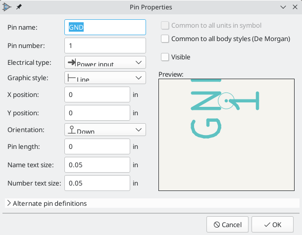
By utworzyć port zasilania, należy wykonać następujące kroki:
-
Add a pin of type "Power input", with "Visible" unchecked, and the pin named according to the desired net. Make the pin number
1, the length0, and set the graphic style to "Line". The pin name establishes the connection to the net; in this case the pin will automatically connect to the netGND. The pin number, length, and line style do not matter electrically. -
Place the pin on the symbol anchor.
-
Use the shape tools to draw the symbol graphics.
-
Set the symbol value. The symbol value does not matter electrically, but it is displayed in the schematic. To eliminate confusion, it should match the pin name (which determines the connected net name).
-
Check the "Define as power symbol" box in Symbol Properties window. This makes the symbol appear in the "Add Power Port" dialog, makes the
Valuefield read-only in the schematic, prevents the symbol from being assigned a footprint, and excludes the symbol from the board, BOM, and netlists. -
Set the symbol reference and uncheck the "Show" box. The reference text is not important except for the first character, which should be
#. For the power port shown above, the reference could be#GND. Symbols with references that begin with#are not added to the PCB, are not included in Bill of Materials exports or netlists, and they cannot be assigned a footprint in the footprint assignment tool. If a power port’s reference does not begin with#, the character will be inserted automatically when the annotation or footprint assignment tools are run.
An easier method to create a new power port symbol is to use another symbol as a starting point, as described earlier.
| The connected net name is determined by the power port’s pin name, not the name or value of the symbol. When modifying an existing power port symbol, make sure to rename the pin so that the new symbol connects to the appropriate power net. This means that power port net names can only be changed in the symbol editor, not in the schematic. |
Przeglądanie bibliotek symboli
Wprowadzenie
The Symbol Library Browser allows you to quickly examine the content of symbol libraries. The Symbol Library Viewer can be accessed by clicking ![]() icon on the main toolbar, View → Symbol Library Browser…, or clicking Select With Browser in the "Choose Symbol" window.
icon on the main toolbar, View → Symbol Library Browser…, or clicking Select With Browser in the "Choose Symbol" window.

Ekran główny
By sprawdzić zawartość biblioteki należy wybrać ją z listy znajdującej się po lewej stronie okna. Wszystkie symbole zostaną pokazane na drugiej liście. Należy wybrać nazwę symbolu by móc go podejrzeć w panelu po prawej stronie.
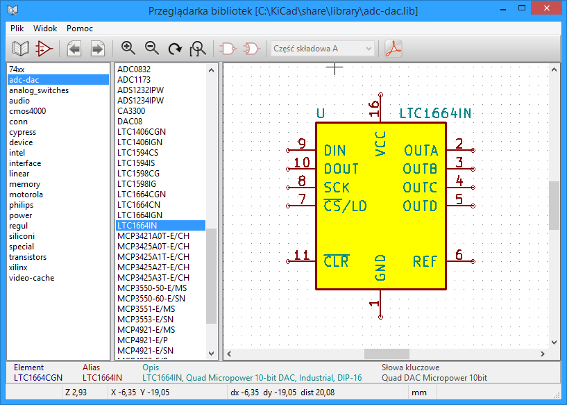
Pasek narzędzi Przeglądarki Bibliotek Symboli
Podstawowy pasek narzędzi wygląda następująco.

Dostępne polecenia to:
|
Selection of the symbol which can be also selected in the displayed list. |
|
Display previous symbol. |
|
Display next symbol. |
|
Zoom tools. |
|
Selection of the representation (normal or alternate) if an alternate representation exists. |
|
Selection of the unit for symbols that contain multiple units. |
|
If they exist, display the associated documents. |
|
Close the browser and place the selected symbol in the schematic. |

Symulator
KiCad provides an embedded electrical circuit simulator using ngspice as the simulation engine.
Podczas pracy z symulatorem przydatna może być oficjalna biblioteka pspice. Zawiera ona popularne symbole używane do symulacji, takie jak źródła napięcia/prądu lub tranzystory z pinami ponumerowanymi tak, aby pasowały do specyfikacji węzłów ngspice.
Istnieje również kilka projektów demonstracyjnych ilustrujących możliwości symulatora. Znajdziesz je w katalogu demos/simulation.
Przypisywanie modeli
Przed uruchomieniem symulacji komponenty muszą mieć przypisany modele Spice.
Każdy komponent może mieć przypisany tylko jeden model, nawet jeśli komponent składa się z wielu jednostek. W takim przypadku pierwsza jednostka powinna mieć określony model.
Komponenty pasywne z referencją pasującą do typu urządzenia w zapisie Spice (R* dla rezystorów, C* dla kondensatorów, L* dla cewek indukcyjnych) będą miały przypisane modele niejawnie i będą używać pola Wartość do określania ich właściwości.
| Należy pamiętać, że w Spice zapis 'M' oznacza mili, a 'Meg' odpowiada Mega. Jeśli wolisz użyć 'M' do wskazania prefiksu Mega, możesz o tym zdecydować w ustawieniach symulatora. |
Informacje o modelu Spice są zapisywane jako tekst w polach symboli, dlatego możesz je zdefiniować w edytorze symboli lub edytorze schematów. Otwórz okno dialogowe właściwości symbolu i kliknij przycisk "Edytuj model Spice", aby otworzyć okno dialogowe "Edytora Modeli Spice".
Okno dialogowe "Edytor Modelu Spice" ma trzy zakładki odpowiadające różnym typom modeli. Istnieją dwie opcje wspólne dla wszystkich typów modeli:
Disable symbol for simulation |
When checked the component is excluded from simulation. |
Alternate node sequence |
Allows one to override symbol pin to model node mapping. To define a different mapping, specify pin numbers in order expected by the model. 'Example:'
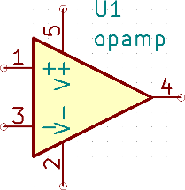
To match the symbol pins to the Spice model nodes shown above, one needs to use an alternate node sequence option with value: "1 3 5 2 4". It is a list of pin numbers corresponding to the Spice model nodes order. |
Pasywne
Zakładka Pasywne pozwala użytkownikowi przypisać pasywny model (rezystor, kondensator lub cewka) do komponentu. Jest to rzadko używana opcja, ponieważ zwykle elementy pasywne mają niejawnie przypisane modele, chyba że odniesienie do komponentu nie jest zgodne z rzeczywistym typem urządzenia.
| Jawnie zdefiniowane model pasywne mają pierwszeństwo przed tymi, które są domyślnie przypisane. Oznacza to, że po przypisaniu pasywnego modelu, pola Odnośnik i Wartość nie są brane pod uwagę podczas symulacji. Może to prowadzić do niejasnej sytuacji, gdy przypisana wartość modelu nie jest zgodna z tą wyświetlaną na schemacie. |
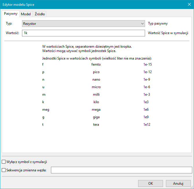
Typ |
Wybór typu elementu (rezystor, kondensator lub cewka). |
Wartość |
Definiuje właściwości komponentu (rezystancja, pojemność lub indukcyjność). Wartość może używać popularnych przedrostków jednostek Spice (wymienionych poniżej pola wprowadzania tekstu) i powinien używać kropki jako separatora dziesiętnego. Zauważ, że interpreter Spice nie działa poprawnie gdy przedrostki przeplatają się w wartości (np. 1k5). |
Model
Zakładka Model służy do przypisania półprzewodnika lub złożonego modelu zdefiniowanego w zewnętrznym pliku biblioteki. Biblioteki modeli Spice są często oferowane przez producentów urządzeń.
Główny widżet tekstowy wyświetla wybraną zawartość z pliku bibliotecznego. Powszechną praktyką jest umieszczanie opisu modeli w plikach biblioteki, w tym kolejności węzłów.
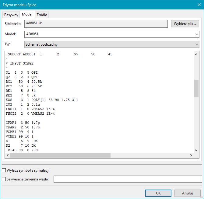
Plik |
Ścieżka do pliku bibliotecznego Spice. Ten plik będzie używany przez symulator, tak jak jest dodawany za pomocą dyrektywy .include. |
Model |
Wybrany model komponentu. Po wybraniu pliku lista jest wypełniana modelami do wyboru. |
Typ |
Wybór typu modelu (inny układ, BJT, MOSFET lub dioda). Zwykle jest ustawiony automatycznie po wybraniu modelu. |
Źródła
Zakładka Źródło służy do przypisania modelu źródła zasilania lub sygnału. Dostępne są dwie sekcje: Analiza DC/AC oraz Analiza czasowa. Każdy definiuje parametry źródłowe dla odpowiedniego typu symulacji.
Opcja Typ źródła jest aktywna dla wszystkich typów symulacji.
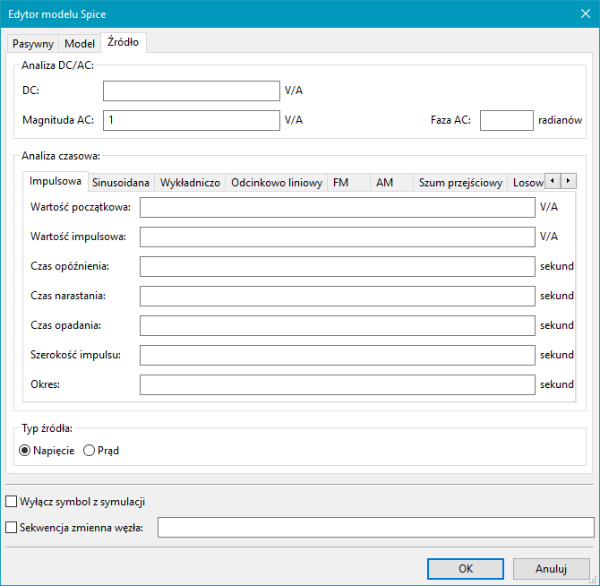
Więcej na temat źródeł w dokumentacji ngspice, rodział 4 (Voltage and Current Sources).
Dyrektywy Spice
It is possible to add Spice directives by placing them in text fields on a schematic sheet. This approach is convenient for defining the default simulation type. This functionality is limited to Spice directives starting with a dot (e.g. .tran 10n 1m), it is not possible to place additional components using text fields.
Symulacja
Aby uruchomić symulację, otwórz okno dialogowe Symulator Spice wybierając menu Narzędzia → Symulator w oknie edytora schematów.
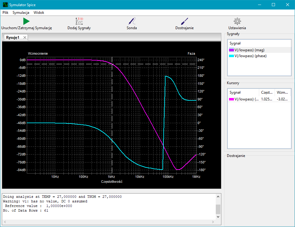
Okno dialogowe posiada kilka sekcji:
Menu
Menu Plik
Nowy wykres |
Tworzy nową kartę w panelu wykresów. |
Otwórz skoroszyt |
Otwiera listę kreślonych sygnałów. |
Zapisz skoroszyt |
Zapisuje listę kreślonych sygnałów. |
Zapisz jako obraz |
Eksportuje aktywny wykres do pliku |
Zapisz jako plik |
Eksportuje aktywne punkty danych surowych wykresu do pliku |
Wyjdź z symulacji |
Zamyka okno dialogowe. |
Symulacja
Uruchom symulację |
Wykonuje symulację przy użyciu bieżących ustawień. |
Dodaj sygnały… |
Otwiera okno dialogowe wyboru sygnałów do kreślenia. |
Sondy ze schematu |
Uruchamia narzędzie typu Sonda. |
Dostrój wartość komponentu |
Uruchom narzędzie Tuner. |
Pokaż listę sieci SPICE… |
Otwiera okno dialogowe pokazujące wygenerowaną listę sieci symulowanego obwodu. |
Ustawienia… |
Otwiera okno dialogowe ustawień symulacji. |
Menu Widok
Powiększ |
Powiększa aktywny wykres. |
Pomniejsz |
Zmniejsza aktywny wykres. |
Dopasuj do ekranu |
Dostosuj ustawienie powiększenia, aby wyświetlić wszystkie wykresy. |
Pokaż siatkę |
Włącza widoczność siatki. |
Pokaż legendę |
Przełącz widoczność legendy wykresu. |
Pasek narzędziowy

Ten pasek umożliwia dostęp do głównych funkcji symulatora.
Uruchom/Zatrzymaj symulację |
Uruchamia lub zatrzymuje symulację. |
Dodaj sygnały |
Otwiera okno dialogowe wyboru sygnałów do wykreślenia. |
Sonda |
Uruchamia narzędzie Sonda. |
Dostrajanie |
Uruchamia narzędzie do dostrajania. |
Ustawienia |
Otwiera okno dialogowe ustawień symulacji. |
Panel wykresu
Pokazuje wyniki symulacji w formie wykresów. W oddzielnych zakładkach można otworzyć wiele wykresów, ale tylko aktywny jest aktualizowany podczas przeprowadzania symulacji. W ten sposób można porównać wyniki symulacji dla różnych przebiegów.
Wykresy można dostosowywać, zmieniając widoczność siatki i legendy za pomocą menu menu Widok. Kiedy legenda jest widoczna, można ją przeciągnąć, aby zmienić jej położenie.
Interakcje w panelu wykresu:
-
kółko myszy służy do przybliżania/oddalania
-
kliknięcie prawym przyciskiem myszy otwiera menu kontekstowe w celu dostosowania widoku
-
zaznaczenie prostokątnego wyboru pozwala powiększyć wybrany obszar
-
przeciągnięcie kursora zmienia jego położenie
Konsola wyjściowa
Konsola wyjścia wyświetla komunikaty z symulatora. Zaleca się sprawdzanie konsoli, aby mieć pewność że nie ma błędów ani ostrzeżeń.
Lista sygnałów
Pokazuje listę sygnałów pokazywanych w aktywnym wykresie.
Interakcje na liście sygnałów:
-
kliknięcie prawym przyciskiem myszy otwiera menu kontekstowe w celu ukrycia sygnału lub przełączenia krusora
-
podwójne kliknięcie ukrywa sygnał
Lista kursorów
Wyświetla listę kursorów i ich współrzędne. Każdy sygnał może mieć wyświetlany jeden kursor. Widoczność kursorów ustawiana jest za pomocą listy sygnałów.
Panel dostrajania
Wyświetla komponenty pobrane za pomocą narzędzia Dostrajanie. Panel dostrajania pozwala użytkownikowi szybko modyfikować wartości komponentów i obserwować ich wpływ na wyniki symulacji - za każdym razem, gdy wartość składnika jest zmieniana, symulacja jest ponownie uruchamiana, a wykresy są aktualizowane.
Z każdym komponentem jest powiązane kilka kontrolek:
-
Górne pole tekstowe określa maksymalną wartość komponentu.
-
Środkowe pole tekstowe określa aktualną wartość komponentu.
-
Dolne pole tekstowe określa minimalną wartość komponentu.
-
Suwak pozwala użytkownikowi modyfikować wartość komponentu w sposób płynny.
-
Przycisk Zapisz modyfikuje wartość komponentu na schemacie do tej wybranej za pomocą suwaka.
-
Przycisk X usuwa komponent z panelu Dostrajanie i przywraca jego oryginalną wartość.
Trzy pola tekstowe rozpoznają przedrostki jednostek używanych przez Spice.
Narzędzie Dostrajanie
Narzędzie dostrajania pozwala użytkownikowi na wybór komponentu, którego wartość chce dostroić.
Aby wybrać komponent by go dostroić, należy kliknąć go w edytorze schematów gdy narzędzie Dostrajanie jest aktywne. Wybrane komponenty pojawią się w panelu Dostrajanie. Tylko pasywne komponenty mogą być dostrajane.
Narzędzie Sonda
Narzędzie Sonda zapewnia przyjazny dla użytkownika sposób wyboru sygnałów w celu umieszczenia ich na wykresie.
Aby dodać sygnał do wykresu, kliknij odpowiednie połączenie w edytorze schematów gdy narzędzie jest aktywne.
Ustawienia symulacji
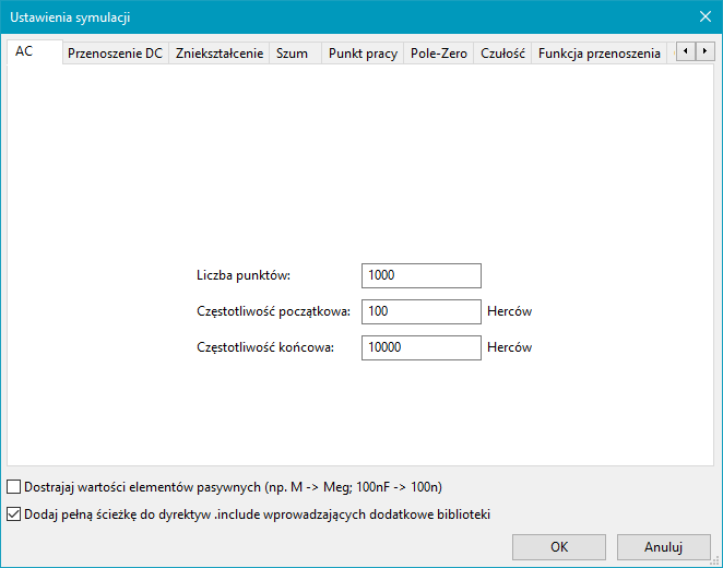
Okno ustawień symulacji pozwala użytkownikowi ustawić typ symulacji i jej parametry. Dostępne są cztery zakładki:
-
AC
-
Przenoszenie DC
-
Analiza czasowa
-
Własne
Pierwsze trzy zakładki zawierają formularze w których można określić parametry symulacji. Ostatnia zakładka umożliwia użytkownikowi wpisanie również niestandardowych dyrektyw Spice. Więcej informacji o typach i parametrach symulacji można znaleźć w dokumentacji ngspice, rozdział 1.2.
Alternatywnym sposobem konfigurowania symulacji jest wpisanie dyrektyw Spice w pola tekstowe na schemacie. Wszystkie dyrektywy pochodzące z pól tekstowych związane z typem symulacji są zastępowane przez ustawienia wybrane w oknie dialogowym. Oznacza to, że gdy rozpoczniemy korzystać z okna dialogowego symulacji, wartości te zastąpią dyrektywy na schemacie do czasu, aż symulator nie zostanie ponownie otwarty.
Istnieją dwie opcje wspólne dla wszystkich typów symulacji:
Dostosuj wartości symboli pasywnych |
Zastąp wartości symboli pasywnych by dokonać często wykonywanej konwersji wartości do ich notacji w Spice. |
Dodaj pełną ścieżkę do dyrektyw .include wprowadzające nowe biblioteki |
Łączy nazwy plików bibliotek modeli Spice z pełną ścieżką dostępu. Normalnie, pełna ścieżka jest wymagana przez ngspice by mógł uzyskać dostęp do pliku biblioteki. |
Advanced Topics
Configuration and Customization
| TODO: write this section |
Text variables
| TODO: write this section |
Custom Netlist and BOM Formats
KiCad can output netlists and BOMs in various formats, and users can define new formats if desired.
The process of exporting a netlist is described in the netlist export section. BOM output is described in the BOM export section.
The following section describes how to create an exporter for a new output format.
Adding new netlist generators
New netlist generators are added to the Export Netlist dialog by clicking the Add Generator… button.
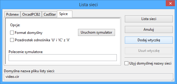
New generators require a name and a command. The name is shown in the tab label, and the command is run whenever the Export Netlist button is clicked.
When the netlist is generated, KiCad creates an intermediate XML file which contains all of the netlist information from the schematic. The generator command is then run in order to transform the intermediate netlist into the desired netlist format.
The netlist command must be set up properly so that the netlist generator script takes the intermediate netlist file as input and outputs the desired netlist file. The exact netlist command will depend on the generator script used. The command format is described below.
Python and XSLT are commonly used tools to create custom netlist generators.
Adding a new BOM generator
KiCad also uses the intermediate netlist file to generate BOMs with the Generate BOM tool.
Additional scripts can be added to the list of BOM generator scripts by clicking the ![]() button. Scripts can be removed by clicking the
button. Scripts can be removed by clicking the ![]() button. The
button. The ![]() button opens the selected script in a text editor.
button opens the selected script in a text editor.
Generator scripts written in Python and XSLT can contain a header comment that describes the generator’s functionality and usage. This header comment is displayed in the BOM dialog as the description for each generator. The header comment must contain the string @package. Everything following that string until the end of the comment is used as the description for the generator.
KiCad automatically fills the command line field when a new generator script is added, but the command line might need to be adjusted by hand depending on the generator script. KiCad attempts to automatically determine the output file extension from the example command line in the generator script’s header.
Generator command line format
The command line for a netlist or BOM exporter defines the command that KiCad will run to generate the selected output file.
For a netlist exporter using xsltproc, an example is:
xsltproc -o %O.net /usr/share/kicad/plugins/netlist_form_pads-pcb.asc.xsl %I
For a BOM exporter using Python, an example is:
/usr/bin/python3 /usr/share/kicad/plugins/bom_csv_grouped_by_value.py "%I" "%O.csv"
It is recommended to surround arguments in the command line with quotes (") in case they contain spaces or other special characters.
|
Some character sequences like %I and %O have a special meaning in the command line, because KiCad replaces them with a filename or path before executing the command.
| Parameter | Replaced with… | Description |
|---|---|---|
|
|
Absolute path and filename of the intermediate netlist file, which is the input to the BOM or netlist generator plugin |
|
|
Absolute path and filename of the output BOM or netlist file (without file
extension). An appropriate file extension may need to be specified after the
|
|
|
Base filename of the output BOM or netlist file (without path or file
extension). An appropriate file extension may need to be specified after the
|
|
|
Absolute path of the project directory, without trailing slash. |
Plik pośredniej listy sieci
When exporting BOM files and netlists, KiCad creates an intermediate netlist file and then runs a separate tool which post-processes the intermediate netlist into the desired netlist or BOM format.
The intermediate netlist uses XML syntax. It contains a large amount of data about the design. Depending on the output (BOM or netlist), different subsets of the complete intermediate netlist file will be included in the final output file.
The structure of the intermediate netlist file is described in detail below.
Because the conversion from intermediate netlist file to output netlist or BOM is a text-to-text transformation, the post-processing filter can be written using Python, XSLT, or any other tool capable of taking XML as input.
XSLT is not recommended for new netlist or BOM exporters; Python or another tool should be used instead. Beginning with KiCad 7, xsltproc is no longer installed with KiCad, although it can be installed separately. Nevertheless, several examples of netlist exporters using XSLT are included below.
|
Plik pośredni listy sieci
Poniższy przykład ukazuje ideę samego pliku pośredniego.
<?xml version="1.0" encoding="utf-8"?>
<export version="D">
  <design>
    <source>F:\kicad_aux\netlist_test\netlist_test.sch</source>
    <date>29/08/2010 21:07:51</date>
    <tool>eeschema (2010-08-28 BZR 2458)-unstable</tool>
  </design>
  <components>
    <comp ref="P1">
      <value>CONN_4</value>
      <libsource lib="conn" part="CONN_4"/>
      <sheetpath names="/" tstamps="/"/>
      <tstamps>4C6E2141</tstamps>
    </comp>
    <comp ref="U2">
      <value>74LS74</value>
      <libsource lib="74xx" part="74LS74"/>
      <sheetpath names="/" tstamps="/"/>
      <tstamps>4C6E20BA</tstamps>
    </comp>
    <comp ref="U1">
      <value>74LS04</value>
      <libsource lib="74xx" part="74LS04"/>
      <sheetpath names="/" tstamps="/"/>
      <tstamps>4C6E20A6</tstamps>
    </comp>
    <comp ref="C1">
      <value>CP</value>
      <libsource lib="device" part="CP"/>
      <sheetpath names="/" tstamps="/"/>
      <tstamps>4C6E2094</tstamps>
    <comp ref="R1">
      <value>R</value>
      <libsource lib="device" part="R"/>
      <sheetpath names="/" tstamps="/"/>
      <tstamps>4C6E208A</tstamps>
    </comp>
  </components>
  <libparts/>
  <libraries/>
  <nets>
    <net code="1" name="GND">
      <node ref="U1" pin="7"/>
      <node ref="C1" pin="2"/>
      <node ref="U2" pin="7"/>
      <node ref="P1" pin="4"/>
    </net>
    <net code="2" name="VCC">
      <node ref="R1" pin="1"/>
      <node ref="U1" pin="14"/>
      <node ref="U2" pin="4"/>
      <node ref="U2" pin="1"/>
      <node ref="U2" pin="14"/>
      <node ref="P1" pin="1"/>
    </net>
    <net code="3" name="">
      <node ref="U2" pin="6"/>
    </net>
    <net code="4" name="">
      <node ref="U1" pin="2"/>
      <node ref="U2" pin="3"/>
    </net>
    <net code="5" name="/SIG_OUT">
      <node ref="P1" pin="2"/>
      <node ref="U2" pin="5"/>
      <node ref="U2" pin="2"/>
    </net>
    <net code="6" name="/CLOCK_IN">
      <node ref="R1" pin="2"/>
      <node ref="C1" pin="1"/>
      <node ref="U1" pin="1"/>
      <node ref="P1" pin="3"/>
    </net>
  </nets>
</export>
Struktura ogólna
Plik pośredni listy sieci posiada 5 sekcji:
-
Sekcja nagłówka.
-
Sekcja komponentów.
-
Sekcja elementów bibliotecznych.
-
Sekcja bibliotek.
-
Sekcja sieci połączeń.
The file content has the delimiter <export>
<export version="D">
...
</export>
Sekcja nagłówka
The header has the delimiter <design>
<design>
<source>F:\kicad_aux\netlist_test\netlist_test.sch</source>
<date>21/08/2010 08:12:08</date>
<tool>eeschema (2010-08-09 BZR 2439)-unstable</tool>
</design>
Sekcja ta może być widoczna jako komentarze.
Sekcja komponentów
The component section has the delimiter <components>
<components>
<comp ref="P1">
<value>CONN_4</value>
<libsource lib="conn" part="CONN_4"/>
<sheetpath names="/" tstamps="/"/>
<tstamps>4C6E2141</tstamps>
</comp>
</components>
Jest to lista na której znajdują się poszczególne komponenty schematu. Każdy komponent jest opisany w następujący sposób:
<comp ref="P1">
<value>CONN_4</value>
<libsource lib="conn" part="CONN_4"/>
<sheetpath names="/" tstamps="/"/>
<tstamps>4C6E2141</tstamps>
</comp>| Element name | Element description |
|---|---|
|
name of the lib where this component was found. |
|
component name inside this library. |
|
path of the sheet inside the hierarchy: identify the sheet within the full schematic hierarchy. |
|
timestamp of the component. |
Note about time stamps for components
To identify a component in a netlist and therefore on a board, the timestamp reference is used as unique for each component. However KiCad provides an auxiliary way to identify a component which is the corresponding footprint on the board. This allows the re-annotation of components in a schematic project and does not lose the link between the component and its footprint.
Znacznik czasowy jest unikalnym identyfikatorem dla każdego składnika lub arkusza schematu w projekcie. Jednak w złożonych hierarchiach, w tym samym arkuszu składnik może być używany więcej niż raz, a zatem arkusz ten zawiera elementy o tym samym znaczniku czasowym.
A given sheet inside a complex hierarchy has an unique identifier: its sheetpath. A given component (inside a complex hierarchy) has a unique identifier: the sheetpath and its timestamp.
Sekcja elementów bibliotecznych
The libparts section has the delimiter <libparts>, and the content of this section is defined in the schematic libraries.
<libparts>
<libpart lib="device" part="CP">
  <description>Condensateur polarise</description>
  <footprints>
    <fp>CP*</fp>
    <fp>SM*</fp>
  </footprints>
  <fields>
    <field name="Reference">C</field>
    <field name="Valeur">CP</field>
  </fields>
  <pins>
    <pin num="1" name="1" type="passive"/>
    <pin num="2" name="2" type="passive"/>
  </pins>
</libpart>
</libparts>| Element name | Element description |
|---|---|
|
The symbol’s footprint filters. Each footprint filter is in a separate |
|
The symbol’s fields. Each field’s name and value is given in a separate `<field name="fieldname">…</field> tag. |
|
The symbol’s pins. Each pin is given in a separate |
Possible electrical pin types are:
| Pintype | Description |
|---|---|
Input |
Usual input pin |
Output |
Usual output |
Bidirectional |
Input or Output |
Tri-state |
Bus input/output |
Passive |
Usual ends of passive components |
Unspecified |
Unknown electrical type |
Power input |
Power input of a component |
Power output |
Power output like a regulator output |
Open collector |
Open collector often found in analog comparators |
Open emitter |
Open emitter sometimes found in logic |
Not connected |
Must be left open in schematic |
Sekcja bibliotek
The libraries section has the delimiter <libraries>. This section contains the list of schematic libraries used in the project.
<libraries>
  <library logical="device">
    <uri>F:\kicad\share\library\device.lib</uri>
  </library>
  <library logical="conn">
    <uri>F:\kicad\share\library\conn.lib</uri>
  </library>
</libraries>
Sekcja sieci
The nets section has the delimiter <nets>. This section describes the connectivity of the schematic by listing all nets and the pins connected to each net.
<nets>
  <net code="1" name="GND">
    <node ref="U1" pin="7"/>
    <node ref="C1" pin="2"/>
    <node ref="U2" pin="7"/>
    <node ref="P1" pin="4"/>
  </net>
  <net code="2" name="VCC">
    <node ref="R1" pin="1"/>
    <node ref="U1" pin="14"/>
    <node ref="U2" pin="4"/>
    <node ref="U2" pin="1"/>
    <node ref="U2" pin="14"/>
    <node ref="P1" pin="1"/>
  </net>
</nets>
Poszczególne sieci są pogrupowane wewnątrz tagu <net>:
<net code="1" name="GND">
  <node ref="U1" pin="7"/>
  <node ref="C1" pin="2"/>
  <node ref="U2" pin="7"/>
  <node ref="P1" pin="4"/>
</net>| Element name | Element Description |
|---|---|
|
an internal identifier for this net |
|
the net name |
|
the pin (identified by |
Example netlist exporters
Some example netlist exporters using XSLT are included below.
XSLT itself is an XML language very suitable for XML transformations. The xsltproc program can be used to read the Intermediate XML netlist input file, apply a style-sheet to transform the input, and save the results in an output file. Use of xsltproc requires a style-sheet file using XSLT conventions. The full conversion process is handled by KiCad, after it is configured once to run xsltproc in a specific way.
The document that describes XSL Transformations (XSLT) is available here: http://www.w3.org/TR/xslt
| When writing a new netlist exporter, consider using Python or another tool rather than XSLT. |
PADS netlist example using XSLT
The following example shows how to create an exporter for the PADS netlist format using xlstproc.
The PADS netlist format is comprised of two sections:
-
A list of footprints
-
A list of nets, together with the pads connected to each net.
Below is an XSL style-sheet which converts the intermediate netlist file to the PADS netlist format.
<?xml version="1.0" encoding="ISO-8859-1"?>
<!--XSL style sheet to Eeschema Generic Netlist Format to PADS netlist format
Copyright (C) 2010, SoftPLC Corporation.
GPL v2.
How to use:
https://lists.launchpad.net/kicad-developers/msg05157.html
-->
<!DOCTYPE xsl:stylesheet [
<!ENTITY nl "
"> <!--new line CR, LF -->
]>
<xsl:stylesheet version="1.0" xmlns:xsl="http://www.w3.org/1999/XSL/Transform">
<xsl:output method="text" omit-xml-declaration="yes" indent="no"/>
<xsl:template match="/export">
<xsl:text>*PADS-PCB*&nl;*PART*&nl;</xsl:text>
<xsl:apply-templates select="components/comp"/>
<xsl:text>&nl;*NET*&nl;</xsl:text>
<xsl:apply-templates select="nets/net"/>
<xsl:text>*END*&nl;</xsl:text>
</xsl:template>
<!-- for each component -->
<xsl:template match="comp">
<xsl:text> </xsl:text>
<xsl:value-of select="@ref"/>
<xsl:text> </xsl:text>
<xsl:choose>
<xsl:when test = "footprint != '' ">
<xsl:apply-templates select="footprint"/>
</xsl:when>
<xsl:otherwise>
<xsl:text>unknown</xsl:text>
</xsl:otherwise>
</xsl:choose>
<xsl:text>&nl;</xsl:text>
</xsl:template>
<!-- for each net -->
<xsl:template match="net">
<!-- nets are output only if there is more than one pin in net -->
<xsl:if test="count(node)>1">
<xsl:text>*SIGNAL* </xsl:text>
<xsl:choose>
<xsl:when test = "@name != '' ">
<xsl:value-of select="@name"/>
</xsl:when>
<xsl:otherwise>
<xsl:text>N-</xsl:text>
<xsl:value-of select="@code"/>
</xsl:otherwise>
</xsl:choose>
<xsl:text>&nl;</xsl:text>
<xsl:apply-templates select="node"/>
</xsl:if>
</xsl:template>
<!-- for each node -->
<xsl:template match="node">
<xsl:text> </xsl:text>
<xsl:value-of select="@ref"/>
<xsl:text>.</xsl:text>
<xsl:value-of select="@pin"/>
<xsl:text>&nl;</xsl:text>
</xsl:template>
</xsl:stylesheet>And here is the PADS netlist output file after running xsltproc:
*PADS-PCB*
*PART*
P1 unknown
U2 unknown
U1 unknown
C1 unknown
R1 unknown
*NET*
*SIGNAL* GND
U1.7
C1.2
U2.7
P1.4
*SIGNAL* VCC
R1.1
U1.14
U2.4
U2.1
U2.14
P1.1
*SIGNAL* N-4
U1.2
U2.3
*SIGNAL* /SIG_OUT
P1.2
U2.5
U2.2
*SIGNAL* /CLOCK_IN
R1.2
C1.1
U1.1
P1.3

*END*
Polecenie które dokonało takiej konwersji wygląda następująco:
kicad\\bin\\xsltproc.exe -o test.net kicad\\bin\\plugins\\netlist_form_pads-pcb.xsl test.tmp
Cadstar netlist example using XSLT
The following example shows how to create an exporter for the Cadstar netlist format using xlstproc.
The Cadstar format is comprised of two sections:
-
The footprint list
-
The Nets list: grouping pads references by nets
Below is an XSL style-sheet which converts the intermediate netlist file to the Cadstar netlist format.
<?xml version="1.0" encoding="ISO-8859-1"?>
<!--XSL style sheet to Eeschema Generic Netlist Format to CADSTAR netlist format
Copyright (C) 2010, Jean-Pierre Charras.
Copyright (C) 2010, SoftPLC Corporation.
GPL v2. -->
<!DOCTYPE xsl:stylesheet [
<!ENTITY nl "
"> <!--new line CR, LF -->
]>
<xsl:stylesheet version="1.0" xmlns:xsl="http://www.w3.org/1999/XSL/Transform">
<xsl:output method="text" omit-xml-declaration="yes" indent="no"/>
<!-- Netlist header -->
<xsl:template match="/export">
<xsl:text>.HEA&nl;</xsl:text>
<xsl:apply-templates select="design/date"/> <!-- Generate line .TIM <time> -->
<xsl:apply-templates select="design/tool"/> <!-- Generate line .APP <eeschema version> -->
<xsl:apply-templates select="components/comp"/> <!-- Generate list of components -->
<xsl:text>&nl;&nl;</xsl:text>
<xsl:apply-templates select="nets/net"/> <!-- Generate list of nets and connections -->
<xsl:text>&nl;.END&nl;</xsl:text>
</xsl:template>
<!-- Generate line .TIM 20/08/2010 10:45:33 -->
<xsl:template match="tool">
<xsl:text>.APP "</xsl:text>
<xsl:apply-templates/>
<xsl:text>"&nl;</xsl:text>
</xsl:template>
<!-- Generate line .APP "eeschema (2010-08-17 BZR 2450)-unstable" -->
<xsl:template match="date">
<xsl:text>.TIM </xsl:text>
<xsl:apply-templates/>
<xsl:text>&nl;</xsl:text>
</xsl:template>
<!-- for each component -->
<xsl:template match="comp">
<xsl:text>.ADD_COM </xsl:text>
<xsl:value-of select="@ref"/>
<xsl:text> </xsl:text>
<xsl:choose>
<xsl:when test = "value != '' ">
<xsl:text>"</xsl:text> <xsl:apply-templates select="value"/> <xsl:text>"</xsl:text>
</xsl:when>
<xsl:otherwise>
<xsl:text>""</xsl:text>
</xsl:otherwise>
</xsl:choose>
<xsl:text>&nl;</xsl:text>
</xsl:template>
<!-- for each net -->
<xsl:template match="net">
<!-- nets are output only if there is more than one pin in net -->
<xsl:if test="count(node)>1">
<xsl:variable name="netname">
<xsl:text>"</xsl:text>
<xsl:choose>
<xsl:when test = "@name != '' ">
<xsl:value-of select="@name"/>
</xsl:when>
<xsl:otherwise>
<xsl:text>N-</xsl:text>
<xsl:value-of select="@code"/>
</xsl:otherwise>
</xsl:choose>
<xsl:text>"&nl;</xsl:text>
</xsl:variable>
<xsl:apply-templates select="node" mode="first"/>
<xsl:value-of select="$netname"/>
<xsl:apply-templates select="node" mode="others"/>
</xsl:if>
</xsl:template>
<!-- for each node -->
<xsl:template match="node" mode="first">
<xsl:if test="position()=1">
<xsl:text>.ADD_TER </xsl:text>
<xsl:value-of select="@ref"/>
<xsl:text>.</xsl:text>
<xsl:value-of select="@pin"/>
<xsl:text> </xsl:text>
</xsl:if>
</xsl:template>
<xsl:template match="node" mode="others">
<xsl:choose>
<xsl:when test='position()=1'>
</xsl:when>
<xsl:when test='position()=2'>
<xsl:text>.TER </xsl:text>
</xsl:when>
<xsl:otherwise>
<xsl:text> </xsl:text>
</xsl:otherwise>
</xsl:choose>
<xsl:if test="position()>1">
<xsl:value-of select="@ref"/>
<xsl:text>.</xsl:text>
<xsl:value-of select="@pin"/>
<xsl:text>&nl;</xsl:text>
</xsl:if>
</xsl:template>
</xsl:stylesheet>Poniżej znajduje się plik wyjściowy dla programu Cadstar.
.HEA
.TIM 21/08/2010 08:12:08
.APP "eeschema (2010-08-09 BZR 2439)-unstable"
.ADD_COM P1 "CONN_4"
.ADD_COM U2 "74LS74"
.ADD_COM U1 "74LS04"
.ADD_COM C1 "CP"
.ADD_COM R1 "R"


.ADD_TER U1.7 "GND"
.TER     C1.2
         U2.7
         P1.4
.ADD_TER R1.1 "VCC"
.TER     U1.14
         U2.4
         U2.1
         U2.14
         P1.1
.ADD_TER U1.2 "N-4"
.TER     U2.3
.ADD_TER P1.2 "/SIG_OUT"
.TER     U2.5
         U2.2
.ADD_TER R1.2 "/CLOCK_IN"
.TER     C1.1
         U1.1
         P1.3

.END
OrcadPCB2 netlist example using XSLT
This format has only one section which is the footprint list. Each footprint includes a list of its pads with reference to a net.
Below is an XSL style-sheet which converts the intermediate netlist file to the Orcad netlist format.
<?xml version="1.0" encoding="ISO-8859-1"?>
<!--XSL style sheet to Eeschema Generic Netlist Format to CADSTAR netlist format
Copyright (C) 2010, SoftPLC Corporation.
GPL v2.
How to use:
https://lists.launchpad.net/kicad-developers/msg05157.html
-->
<!DOCTYPE xsl:stylesheet [
<!ENTITY nl "
"> <!--new line CR, LF -->
]>
<xsl:stylesheet version="1.0" xmlns:xsl="http://www.w3.org/1999/XSL/Transform">
<xsl:output method="text" omit-xml-declaration="yes" indent="no"/>
<!--
Netlist header
Creates the entire netlist
(can be seen as equivalent to main function in C
-->
<xsl:template match="/export">
<xsl:text>( { Eeschema Netlist Version 1.1 </xsl:text>
<!-- Generate line .TIM <time> -->
<xsl:apply-templates select="design/date"/>
<!-- Generate line eeschema version ... -->
<xsl:apply-templates select="design/tool"/>
<xsl:text>}&nl;</xsl:text>
<!-- Generate the list of components -->
<xsl:apply-templates select="components/comp"/> <!-- Generate list of components -->
<!-- end of file -->
<xsl:text>)&nl;*&nl;</xsl:text>
</xsl:template>
<!--
Generate id in header like "eeschema (2010-08-17 BZR 2450)-unstable"
-->
<xsl:template match="tool">
<xsl:apply-templates/>
</xsl:template>
<!--
Generate date in header like "20/08/2010 10:45:33"
-->
<xsl:template match="date">
<xsl:apply-templates/>
<xsl:text>&nl;</xsl:text>
</xsl:template>
<!--
This template read each component
(path = /export/components/comp)
creates lines:
( 3EBF7DBD $noname U1 74LS125
... pin list ...
)
and calls "create_pin_list" template to build the pin list
-->
<xsl:template match="comp">
<xsl:text> ( </xsl:text>
<xsl:choose>
<xsl:when test = "tstamp != '' ">
<xsl:apply-templates select="tstamp"/>
</xsl:when>
<xsl:otherwise>
<xsl:text>00000000</xsl:text>
</xsl:otherwise>
</xsl:choose>
<xsl:text> </xsl:text>
<xsl:choose>
<xsl:when test = "footprint != '' ">
<xsl:apply-templates select="footprint"/>
</xsl:when>
<xsl:otherwise>
<xsl:text>$noname</xsl:text>
</xsl:otherwise>
</xsl:choose>
<xsl:text> </xsl:text>
<xsl:value-of select="@ref"/>
<xsl:text> </xsl:text>
<xsl:choose>
<xsl:when test = "value != '' ">
<xsl:apply-templates select="value"/>
</xsl:when>
<xsl:otherwise>
<xsl:text>"~"</xsl:text>
</xsl:otherwise>
</xsl:choose>
<xsl:text>&nl;</xsl:text>
<xsl:call-template name="Search_pin_list" >
<xsl:with-param name="cmplib_id" select="libsource/@part"/>
<xsl:with-param name="cmp_ref" select="@ref"/>
</xsl:call-template>
<xsl:text> )&nl;</xsl:text>
</xsl:template>
<!--
This template search for a given lib component description in list
lib component descriptions are in /export/libparts,
and each description start at ./libpart
We search here for the list of pins of the given component
This template has 2 parameters:
"cmplib_id" (reference in libparts)
"cmp_ref" (schematic reference of the given component)
-->
<xsl:template name="Search_pin_list" >
<xsl:param name="cmplib_id" select="0" />
<xsl:param name="cmp_ref" select="0" />
<xsl:for-each select="/export/libparts/libpart">
<xsl:if test = "@part = $cmplib_id ">
<xsl:apply-templates name="build_pin_list" select="pins/pin">
<xsl:with-param name="cmp_ref" select="$cmp_ref"/>
</xsl:apply-templates>
</xsl:if>
</xsl:for-each>
</xsl:template>
<!--
This template writes the pin list of a component
from the pin list of the library description
The pin list from library description is something like
<pins>
<pin num="1" type="passive"/>
<pin num="2" type="passive"/>
</pins>
Output pin list is ( <pin num> <net name> )
something like
( 1 VCC )
( 2 GND )
-->
<xsl:template name="build_pin_list" match="pin">
<xsl:param name="cmp_ref" select="0" />
<!-- write pin numner and separator -->
<xsl:text> ( </xsl:text>
<xsl:value-of select="@num"/>
<xsl:text> </xsl:text>
<!-- search net name in nets section and write it: -->
<xsl:variable name="pinNum" select="@num" />
<xsl:for-each select="/export/nets/net">
<!-- net name is output only if there is more than one pin in net
else use "?" as net name, so count items in this net
-->
<xsl:variable name="pinCnt" select="count(node)" />
<xsl:apply-templates name="Search_pin_netname" select="node">
<xsl:with-param name="cmp_ref" select="$cmp_ref"/>
<xsl:with-param name="pin_cnt_in_net" select="$pinCnt"/>
<xsl:with-param name="pin_num"> <xsl:value-of select="$pinNum"/>
</xsl:with-param>
</xsl:apply-templates>
</xsl:for-each>
<!-- close line -->
<xsl:text> )&nl;</xsl:text>
</xsl:template>
<!--
This template writes the pin netname of a given pin of a given component
from the nets list
The nets list description is something like
<nets>
<net code="1" name="GND">
<node ref="J1" pin="20"/>
<node ref="C2" pin="2"/>
</net>
<net code="2" name="">
<node ref="U2" pin="11"/>
</net>
</nets>
This template has 2 parameters:
"cmp_ref" (schematic reference of the given component)
"pin_num" (pin number)
-->
<xsl:template name="Search_pin_netname" match="node">
<xsl:param name="cmp_ref" select="0" />
<xsl:param name="pin_num" select="0" />
<xsl:param name="pin_cnt_in_net" select="0" />
<xsl:if test = "@ref = $cmp_ref ">
<xsl:if test = "@pin = $pin_num">
<!-- net name is output only if there is more than one pin in net
else use "?" as net name
-->
<xsl:if test = "$pin_cnt_in_net>1">
<xsl:choose>
<!-- if a net has a name, use it,
else build a name from its net code
-->
<xsl:when test = "../@name != '' ">
<xsl:value-of select="../@name"/>
</xsl:when>
<xsl:otherwise>
<xsl:text>$N-0</xsl:text><xsl:value-of select="../@code"/>
</xsl:otherwise>
</xsl:choose>
</xsl:if>
<xsl:if test = "$pin_cnt_in_net <2">
<xsl:text>?</xsl:text>
</xsl:if>
</xsl:if>
</xsl:if>
</xsl:template>
</xsl:stylesheet>Poniżej znajduje się plik wyjściowy programu OrcadPCB2.
( { Eeschema Netlist Version 1.1  29/08/2010 21:07:51
eeschema (2010-08-28 BZR 2458)-unstable}
 ( 4C6E2141 $noname P1 CONN_4
  (  1 VCC )
  (  2 /SIG_OUT )
  (  3 /CLOCK_IN )
  (  4 GND )
 )
 ( 4C6E20BA $noname U2 74LS74
  (  1 VCC )
  (  2 /SIG_OUT )
  (  3 N-04 )
  (  4 VCC )
  (  5 /SIG_OUT )
  (  6 ? )
  (  7 GND )
  (  14 VCC )
 )
 ( 4C6E20A6 $noname U1 74LS04
  (  1 /CLOCK_IN )
  (  2 N-04 )
  (  7 GND )
  (  14 VCC )
 )
 ( 4C6E2094 $noname C1 CP
  (  1 /CLOCK_IN )
  (  2 GND )
 )
 ( 4C6E208A $noname R1 R
  (  1 VCC )
  (  2 /CLOCK_IN )
 )
)
*
Actions reference
Below is a list of every available action in the KiCad Schematic Editor: a command that can be assigned to a hotkey.
Schematic Editor
The actions below are available in the Schematic Editor. Hotkeys can be assigned to any of these actions in the Hotkeys section of the preferences.
| Action | Default Hotkey | Description |
|---|---|---|
Align Elements to Grid |
||
Annotate Schematic… |
Fill in schematic symbol reference designators |
|
Assign Footprints… |
Run footprint assignment tool |
|
Clear Net Highlighting |
~ |
Clear any existing net highlighting |
Export Drawing to Clipboard |
Export drawing of current sheet to clipboard |
|
Edit Library Symbol… |
Ctrl+Shift+E |
Open the library symbol in the Symbol Editor |
Edit Sheet Page Number… |
Edit the page number of the current or selected sheet |
|
Edit Symbol Fields… |
Bulk-edit fields of all symbols in schematic |
|
Edit Symbol Library Links… |
Edit links between schematic and library symbols |
|
Edit with Symbol Editor |
Ctrl+E |
Open the selected symbol in the Symbol Editor |
Highlight on PCB |
Highlight corresponding items in PCB editor |
|
Export Netlist… |
Export file containing netlist in one of several formats |
|
Force H/V Wires and Buses |
Switch H & V only mode for new wires and buses |
|
Generate BOM… |
Generate a bill of materials for the current schematic |
|
Highlight Net |
` |
Highlight net under cursor |
Highlight Nets |
Highlight wires and pins of a net |
|
Import Footprint Assignments… |
Import symbol footprint assignments from .cmp file created by Pcbnew |
|
Remap Legacy Library Symbols… |
Remap library symbol references in legacy schematics to the symbol library table |
|
Repair Schematic |
Run various diagnostics and attempt to repair schematic |
|
Rescue Symbols… |
Find old symbols in project and rename/rescue them |
|
Simulator… |
Simulate circuit in SPICE |
|
Save Current Sheet Copy As… |
Save a copy of the current sheet to another location or name |
|
Schematic Setup… |
Edit schematic setup including annotation styles and electrical rules |
|
Bus Definitions… |
Manage bus definitions |
|
Show Hidden Fields |
Toggle display of hidden text fields |
|
Show Hidden Pins |
Toggle display of hidden pins |
|
Switch to PCB Editor |
Open PCB in board editor |
|
Scripting Console |
Show the Python scripting console |
|
Symbol Checker |
Show the symbol checker window |
|
Electrical Rules Checker |
Perform electrical rules check |
|
Show Datasheet |
D |
Opens the datasheet in a browser |
Add Sheet |
S |
Add a hierarchical sheet |
Finish Sheet |
Finish drawing sheet |
|
Import Sheet Pin |
Import a hierarchical sheet pin |
|
Import Sheet Pin |
Import a hierarchical sheet pin |
|
Add Wire to Bus Entry |
Z |
Add a wire entry to a bus |
Add Global Label |
Ctrl+L |
Add a global label |
Add Hierarchical Label |
H |
Add a hierarchical label |
Add Image |
Add bitmap image |
|
Add Junction |
J |
Add a junction |
Add Label |
L |
Add a net label |
Add No Connect Flag |
Q |
Add a no-connection flag |
Add Power |
P |
Add a power port |
Add Text |
T |
Add text |
Add Symbol |
A |
Add a symbol |
Add Junctions to Selection where needed |
||
Add Bus |
B |
Add a bus |
Add Lines |
I |
Add connected graphic lines |
Add Wire |
W |
Add a wire |
Finish Wire or Bus |
K |
Complete drawing at current segment |
Finish Bus |
Complete bus with current segment |
|
Finish Lines |
Complete connected lines with current segment |
|
Finish Wire |
Complete wire with current segment |
|
Unfold from Bus |
C |
Break a wire out of a bus |
Assign Netclass… |
Assign a netclass to the net of the selected wire |
|
Autoplace Fields |
O |
Runs the automatic placement algorithm on the symbol or sheet’s fields |
Break Bus |
Divide a bus into segments which can be dragged independently |
|
Break Wire |
Divide a wire into segments which can be dragged independently |
|
Change Symbol… |
Assign a different symbol from the library |
|
Change Symbols… |
Assign different symbols from the library |
|
Cleanup Sheet Pins |
Delete unreferenced sheet pins |
|
Edit Footprint… |
F |
Displays footprint field dialog |
Edit Reference Designator… |
U |
Displays reference designator dialog |
Edit Text & Graphics Properties… |
Edit text and graphics properties globally across schematic |
|
Edit Value… |
V |
Displays value field dialog |
Mirror Horizontally |
X |
Flips selected item(s) from left to right |
Mirror Vertically |
Y |
Flips selected item(s) from top to bottom |
Pin Table… |
Displays pin table for bulk editing of pins |
|
Properties… |
E |
Displays item properties dialog |
Repeat Last Item |
Ins |
Duplicates the last drawn item |
Rotate Counterclockwise |
R |
Rotates selected item(s) counter-clockwise |
Rotate Clockwise |
Rotates selected item(s) clockwise |
|
De Morgan Alternate |
Switch to alternate De Morgan representation |
|
De Morgan Standard |
Switch to standard De Morgan representation |
|
Symbol Properties… |
Displays symbol properties dialog |
|
Change to Global Label |
Change existing item to a global label |
|
Change to Hierarchical Label |
Change existing item to a hierarchical label |
|
Change to Label |
Change existing item to a label |
|
Change to Text |
Change existing item to a text comment |
|
De Morgan Conversion |
Switch between De Morgan representations |
|
Update Symbol… |
Update symbol to include any changes from the library |
|
Update Symbols from Library… |
Update symbols to include any changes from the library |
|
Move Activate |
||
Drag |
G |
Drags the selected item(s) |
Move |
M |
Moves the selected item(s) |
Select Connection |
Alt+4 |
Select a complete connection |
Select Node |
Alt+3 |
Select a connection item under the cursor |
Enter Sheet |
Display the selected sheet’s contents in the schematic editor |
|
Navigate to page |
Navigate to page |
|
Leave Sheet |
Alt+Back |
Display the parent sheet in the schematic editor |
Hierarchy Navigator |
Show schematic sheet hierarchy |
|
Push Pin Length |
Copy pin length to other pins in symbol |
|
Push Pin Name Size |
Copy pin name size to other pins in symbol |
|
Push Pin Number Size |
Copy pin number size to other pins in symbol |
|
Create Corner |
Create a corner |
|
Remove Corner |
Remove corner |
|
Add a simulator probe |
||
Select a value to be tuned |
||
Add Arc |
Add an arc |
|
Add Circle |
Add a circle |
|
Add Lines |
Add connected graphic lines |
|
Add Rectangle |
Add a rectangle |
|
Finish Drawing |
Finish drawing shape |
|
Move Symbol Anchor |
Specify a new location for the symbol anchor |
|
Add Pin |
P |
Add a pin |
Add Text |
Add a text item |
|
Add Symbol to Schematic |
Add Symbol to Schematic |
|
Copy |
||
Cut |
||
Delete Symbol |
Remove the selected symbol from its library |
|
Duplicate Symbol |
Make a copy of the selected symbol |
|
Edit Symbol |
Show selected symbol on editor canvas |
|
Export… |
Export a symbol to a new library file |
|
Export Symbol as SVG… |
Create SVG file from the current symbol |
|
Export View as PNG… |
Create PNG file from the current view |
|
Hide Symbol Tree |
||
Import Symbol… |
Import a symbol to the current library |
|
New Symbol… |
N |
Create a new symbol |
Paste Symbol |
||
Save Library As… |
Ctrl+Shift+S |
Save the current library to a new file. |
Save As… |
Save the current symbol to a different library. |
|
Show Pin Electrical Types |
Annotate pins with their electrical types |
|
Show Symbol Tree |
||
Synchronized Pins Edit Mode |
Synchronized Pins Edit Mode When enabled propagates all changes (except pin numbers) to other units. Enabled by default for multiunit parts with interchangeable units. |
|
Update Symbol Fields… |
Update symbol to match changes made in parent symbol |
|
Symbol Move Activate |
Common
The actions below are available across KiCad, including in the Schematic Editor. Hotkeys can be assigned to any of these actions in the Hotkeys section of the preferences.
| Action | Default Hotkey | Description |
|---|---|---|
Exclude Marker |
Mark current violation in Checker window as an exclusion |
|
Next Marker |
Go to next marker in Checker window |
|
Previous Marker |
Go to previous marker in Checker window |
|
Add Library… |
Add an existing library folder |
|
Click |
Return |
Performs left mouse button click |
Double-click |
End |
Performs left mouse button double-click |
Cursor Down |
Down |
|
Cursor Down Fast |
Ctrl+Down |
|
Cursor Left |
Left |
|
Cursor Left Fast |
Ctrl+Left |
|
Cursor Right |
Right |
|
Cursor Right Fast |
Ctrl+Right |
|
Cursor Up |
Up |
|
Cursor Up Fast |
Ctrl+Up |
|
Switch to Fast Grid 1 |
Alt+1 |
|
Switch to Fast Grid 2 |
Alt+2 |
|
Switch to Next Grid |
N |
|
Switch to Previous Grid |
Shift+N |
|
Grid Properties… |
Set grid dimensions |
|
Reset Grid Origin |
Z |
|
Grid Origin |
S |
Set the grid origin point |
Inactive Layer View Mode |
Toggle inactive layers between normal and dimmed |
|
Inactive Layer View Mode (3-state) |
H |
Cycle inactive layers between normal, dimmed, and hidden |
Inches |
Use inches |
|
Millimeters |
Use millimeters |
|
Mils |
Use mils |
|
New… |
Ctrl+N |
Create a new document in the editor |
New Library… |
Create a new library folder |
|
Open… |
Ctrl+O |
Open existing document |
Page Settings… |
Settings for paper size and title block info |
|
Pan Down |
Shift+Down |
|
Pan Left |
Shift+Left |
|
Pan Right |
Shift+Right |
|
Pan Up |
Shift+Up |
|
Pin Library |
Keep the library at the top of the list |
|
Plot… |
Plot |
|
Print… |
Ctrl+P |
|
Quit |
Close the current editor |
|
Reset Local Coordinates |
Space |
|
Revert |
Throw away changes |
|
Save |
Ctrl+S |
Save changes |
Save All |
Save all changes |
|
Save As… |
Ctrl+Shift+S |
Save current document to another location |
Save Copy As… |
Save a copy of the current document to another location |
|
3D Viewer |
Alt+3 |
Show 3D viewer window |
Show Context Menu |
Perform the right-mouse-button action |
|
Footprint Library Browser |
Browse footprint libraries |
|
Footprint Editor |
Create, delete and edit footprints |
|
Symbol Library Browser |
Browse symbol libraries |
|
Symbol Editor |
Create, delete and edit symbols |
|
Always Show Cursor |
Ctrl+Shift+X |
Display crosshairs even in selection tool |
Full-Window Crosshairs |
Switch display of full-window crosshairs |
|
Show Grid |
Display grid dots or lines in the edit window |
|
Polar Coordinates |
Switch between polar and cartesian coordinate systems |
|
Switch units |
Ctrl+U |
Switch between imperial and metric units |
Unpin Library |
No longer keep the library at the top of the list |
|
Update PCB from Schematic… |
F8 |
Update PCB with changes made to schematic |
Update Schematic from PCB… |
Update schematic with changes made to PCB |
|
Center |
F4 |
Center |
Zoom to Objects |
Ctrl+Home |
Zoom to Objects |
Zoom to Fit |
Home |
Zoom to Fit |
Zoom In at Cursor |
F1 |
Zoom In at Cursor |
Zoom In |
Zoom In |
|
Zoom Out at Cursor |
F2 |
Zoom Out at Cursor |
Zoom Out |
Zoom Out |
|
Refresh |
F5 |
Refresh |
Zoom to Selection |
Ctrl+F5 |
Zoom to Selection |
Cancel |
Cancel current tool |
|
Change Edit Method |
Ctrl+Space |
Change edit method constraints |
Copy |
Ctrl+C |
Copy selected item(s) to clipboard |
Cut |
Ctrl+X |
Cut selected item(s) to clipboard |
Delete |
Del |
Deletes selected item(s) |
Interactive Delete Tool |
Delete clicked items |
|
Duplicate |
Ctrl+D |
Duplicates the selected item(s) |
Find |
Ctrl+F |
Find text |
Find and Replace |
Ctrl+Alt+F |
Find and replace text |
Find Next |
F3 |
Find next match |
Find Next Marker |
Shift+F3 |
|
Paste |
Ctrl+V |
Paste item(s) from clipboard |
Paste Special… |
Paste item(s) from clipboard with options |
|
Redo |
Ctrl+Y |
Redo last edit |
Replace All |
Replace all matches |
|
Replace and Find Next |
Replace current match and find next |
|
Select All |
Ctrl+A |
Select all items on screen |
Undo |
Ctrl+Z |
Undo last edit |
Measure Tool |
Ctrl+Shift+M |
Interactively measure distance between points |
Select item(s) |
Select item(s) |
|
Configure Paths… |
Edit path configuration environment variables |
|
Donate |
Open "Donate to KiCad" in a web browser |
|
Get Involved |
Open "Contribute to KiCad" in a web browser |
|
Getting Started with KiCad |
Open “Getting Started in KiCad” guide for beginners |
|
Help |
Open product documentation in a web browser |
|
List Hotkeys… |
Ctrl+F1 |
Displays current hotkeys table and corresponding commands |
Preferences… |
Ctrl+, |
Show preferences for all open tools |
Report Bug |
Report a problem with KiCad |
|
Manage Footprint Libraries… |
Edit the global and project footprint library lists |
|
Manage Symbol Libraries… |
Edit the global and project symbol library lists |