编辑电路板
放置和绘制操作
放置和绘图工具位于右侧工具栏中。 当一个工具被激活时,它将一直处于激活状态,直到选择了一个不同的工具或用 Esc 键取消该工具。 当任何其他工具被取消时,选择工具总是被激活。
某些工具栏按钮在调色板中有多个可用工具。这些工具由按钮右下角的小箭头表示:
要显示调色板,你可以在工具上点击并按住鼠标按钮,或者点击并拖动鼠标。 调色板关闭时将显示最近使用的工具。
|
Selection tool (the default tool). When the rectangular selection mode is active, clicking and dragging performs a rectangular selection. When the lasso selection mode is active, clicking and dragging performs a lasso selection. |
|
Local ratsnest tool: when the board ratsnest is hidden, selecting footprints with this tool will show the ratsnest for the selected footprint only. Selecting the same footprint again will hide its ratsnest. The local ratsnest setting for each footprint will remain in effect even after the local ratsnest tool is no longer active. |
|
Footprint placement tool: click on the board to open the footprint chooser, then click again after choosing a footprint to confirm its location. |
|
Route tracks / route differential pairs: These tools activate the interactive router and allow placing tracks and vias. The interactive router is described in more detail in the Routing Tracks section. |
|
Tune length: These tools allow you to tune the length of single tracks or the length or skew of differential pairs, after they have been routed. |
|
Add vias: place a standalone ("free") via without routing tracks. |
|
Add filled zone: Click to set the start point of a zone, then configure its properties before drawing the rest of the zone outline. Zone properties are described in more detail below. |
|
Add rule area: Rule areas, formerly known as keepouts, can restrict item placement and zone fills. You can also define named areas and apply specific custom DRC rules to them. |
|
Note: Lines are graphical objects and are not the same as tracks placed with the Route Tracks tool. |
|
Draw arcs: pick the center point of the arc, then the start and end points. By right clicking this button, you can change the arc editing mode between a mode that maintains the existing arc center and a mode that maintains the arc radius. |
|
Draw rectangles. Rectangles can be filled or outlines. |
|
Draw circles. Circles can be filled or outlines. |
|
Draw graphical polygons. Polygons can be filled or outlined. Note: Filled graphical polygons are not the same as filled zones: graphical polygons cannot be assigned to a net and will not keep clearance from other items. |
|
Draw bezier curves. Each click alternates between fixing a curve node and fixing the control handle for the node that was just placed. |
|
Add bitmap image for reference. Reference images are not included in fabrication outputs. |
|
|
|
|
|
|
|
|
|
Deletion tool: click objects to delete them. |
|
Set grid origin or drill/place origin (used for fabrication outputs). |
|
Interactively measure the distance between two points. |
Grids and snapping
When moving, dragging, and drawing board elements, you can make these operations snap to a grid or to snapping points on pads and other items. In complex designs, snap points can be so close together that it makes the current tool action difficult. Both grid and object snapping can be disabled while moving the mouse by using the modifier keys in the table below.
| On Apple keyboards, use the Cmd key instead of Ctrl. |
| Modifier Key | Effect |
|---|---|
Ctrl |
Disable grid snapping. |
Shift |
Disable object snapping. |
Tools only snap to objects on visible layers. You can reduce unwanted snapping points by hiding unneeded layers or using the single-layer view mode. Additionally, you can toggle between snapping to objects on all layers or only snapping to objects on the current layer by pressing Shift+S.
Snapping to different types of objects (pads, tracks, and graphics) can be configured in the Editing Options section of the PCB Editor preferences.
Snapping to graphical shapes
When working with graphic shapes like rectangles or arcs, such as when drawing shapes or when selecting a reference point for a move operation, many additional snapping points are available that let you snap to features of existing graphic shapes.
Available snapping points for graphic shapes include:
-
Endpoints and corners
-
Midpoints
-
Centers
-
Intersection points
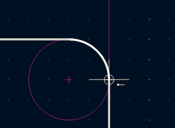
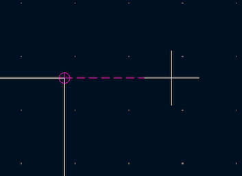
When you hover over a snap point with a shape tool active, a graphical icon will be shown that indicates a snapping point is active and explains the type of snapping point. Clicking will use that snapping point. Some shapes display auxiliary snapping lines that appear when you snap to part of that object. For example, line segments display an auxiliary line that continues the segment beyond its endpoint, and arcs display an auxiliary circle that completes the arc’s circumference. Auxiliary shapes can be used for snapping just like the original shape. An auxiliary line and circle are shown as a solid purple line in the screenshot below. The cursor indicates that the active snapping point is the endpoint of a line.
If you move the cursor away from the snapping point, a horizontal or vertical dashed line will appear, depending on the direction of motion. This indicates a horizontal or vertical projection from the snapping point, respectively. Following the line will maintain a position that is horizontally or vertically aligned to the original snap point. This projection is shown as a purple dashed line in the screenshot below.
Grid settings
Interactive editing operations are snapped to the active grid. You can adjust the grid size using the grid dropdown in the top toolbar or by right-clicking and selecting a new grid from the list in the Grid submenu. Pressing the n or N hotkeys will cycle to the next and previous grid in the list, respectively.
You can also select a new grid or edit the available grids in the Grids pane of the preferences dialog. As a shortcut to reach this dialog, right click the ![]() button on the left toolbar and select Edit Grids….
button on the left toolbar and select Edit Grids….
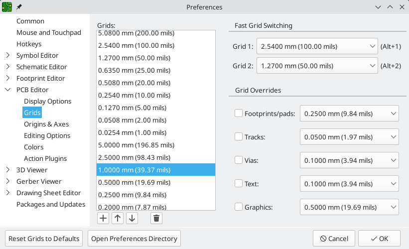
In this dialog you can select an active grid from the list of grids, reorder the list of grids (![]() /
/ ![]() ), and add (
), and add (![]() ), remove (
), remove (![]() ), or edit (
), or edit (![]() ) grids. Grids defined in this dialog can have unequal X and Y spacing as well as an optional name. The grid spacing and name are specified when you create or edit a grid.
) grids. Grids defined in this dialog can have unequal X and Y spacing as well as an optional name. The grid spacing and name are specified when you create or edit a grid.
This dialog also lets you designate two grids from the list as "Fast Grids", which can be quickly selected using Alt+1 and Alt+2.
Finally, you can configure grid overrides for different types of objects. Grid overrides let you set particular grid sizes for different types of objects which will be used instead of the default grid when working with those objects. For example, you can set a 100 mil grid for footprints and pads while using smaller grids to finely position tracks, vias, and text. Grid overrides can be individually enabled and disabled in this dialog, or globally enabled and disabled using the ![]() button on the left toolbar (Ctrl+Shift+G).
button on the left toolbar (Ctrl+Shift+G).
To change the origin (zero point) of the grid, use Place → Grid Origin and click to place the origin in the canvas. This function is also available with the ![]() button in the right toolbar. Alternatively, you can enter explicit coordinates for the grid origin with Edit → Grid Origin….
button in the right toolbar. Alternatively, you can enter explicit coordinates for the grid origin with Edit → Grid Origin….
| The grid origin is one of several different origins in KiCad, which aren’t necessarily set to the same point. The grid origin is the point that the grid aligns to; shifting the grid origin also shifts every grid point. The page origin is an absolute origin which is always the top left corner of the drawing sheet. The drill/place file origin is a configurable point that can be used for fabrication outputs (Place → Drill/Place File Origin). Finally, the local origin is a quickly settable relative origin that current cursor location by pressing Space; the cursor coordinates relative to the local origin are displayed in the status bar. |
The visual appearance of the grid can also be customized in several ways. You can change the thickness of the grid markings, switch their shape (dots, lines, or crosses), and set the minimum displayed spacing in the Display Options page of the preferences dialog, and you can change the grid color in the Colors page of the preferences dialog.
The grid can be shown or hidden using the ![]() button on the left-hand toolbar. By default the grid is still active even if it is hidden, but this is configurable in the Display Options preferences page. There you can set the grid to be disabled when it is hidden or even disable the grid entirely.
button on the left-hand toolbar. By default the grid is still active even if it is hidden, but this is configurable in the Display Options preferences page. There you can set the grid to be disabled when it is hidden or even disable the grid entirely.
编辑对象属性
All objects have properties that are editable in a dialog. Use the hotkey E or select Properties from the right-click context menu to edit the properties of selected item(s). You can only open the properties dialog if all the items you have selected are of the same type. For many object types, like footprints, you can only edit the properties of a single item at one time. To edit the properties of multiple items at once, including items with different types, you can use the Properties Manager.
You can also view and edit item properties using the Properties Manager. The Properties Manager is a docked panel that displays the properties of the selected item or items for editing. If multiple types of items are selected at once, the properties panel displays only the properties shared by all of the selected item types.
Editing a property in the Properties Manager immediately applies the change. When multiple items are selected, property modifications are applied to each selected item individually, not to the whole selection as a group. For example, when changing the orientation of multiple items, each item is individually rotated around its own origin, not the group’s origin.
Show the Properties Manager with View → Panels → Properties or the ![]() button on the left toolbar.
button on the left toolbar.
Several tools are available for editing properties of specific types of objects in bulk. For text and graphical items, including footprint fields and dimensions, you can use the Edit Text and Graphics Properties tool. Tracks and vias can be bulk-edited using the Edit Track and Via Properties tool. Teardrop properties can be edited with the Edit Teardrops tool.
In properties dialogs and many other dialogs, any field that contains a numeric value can also accept a basic math expression that results in a numeric value.
For example, a dimension may be entered as 2 * 2mm, resulting in a value of 4mm. Basic arithmetic operators as well as parentheses for defining order of operations are supported. Units can also be specified, and unit conversions are performed automatically, so 1in + 1mm evaluates to 26.4mm.
电路板边框 (Edge Cuts)
KiCad 使用 Edge.Cuts 层上的图形对象来定义电路板的边框。 边框必须是一个连续(封闭)的形状,但可以由不同类型的图形对象组成,如直线和弧,或者是一个单一的对象,如矩形或多边形。 如果没有定义电路板的边框,或者电路板的边框无效,那么一些功能,如 3D 查看器和一些设计规则的检查将无法发挥作用。
For the board outline to be considered valid, the endpoints of any shapes in the outline must coincide exactly. If any endpoints are not coincident with another endpoint, the outline will not be considered closed. Outline shapes also cannot intersect each other or overlap. In such cases, DRC will report a "Board has malformed outline" violation that points to the problematic parts of the outline.
| You can use the grid or the snapping tools to ensure outline endpoints exactly coincide. The Heal Shapes tool can also be used to fix small gaps between endpoints. |
If there are multiple closed shapes on the Edge.Cuts layer, each shape acts as an independent board outline. When an outline shape completely encloses another outline, the outermost shape is considered the outside edge of the board. Any closed shapes inside the outer shape are considered interior cutouts in the board. Each closed outline cannot intersect or overlap with other outlines.
Zones only fill when they are within the board outline. Any portion of a zone that is outside of the board outline, including inside an interior cutout, will not be filled.
使用封装
Adding footprints to the board
Footprints are automatically added to the board when the PCB is updated from the schematic. The footprint associated with each schematic symbol is added to the board if it is not already present, and each footprint pad is associated with the corresponding symbol pin’s net. Symbol pins are matched to footprint pads by pin/pad number.
When footprints are added to the board after an update from the schematic, they are clustered by schematic sheet and by geographical location in the schematic. They are initially attached to the cursor; you can place them by clicking in the desired location.
You can also add footprints to the board manually using the Add Footprint tool (A or the ![]() button).
button).
| Footprints added in this way will not be automatically associated with a symbol or have nets assigned to their pads, and subsequent updates from the schematic will remove these unassociated footprints unless the footprint is locked or the Delete footprints with no symbols option is unchecked in the Update PCB From Schematic dialog. For these reasons, it is usually recommended to avoid manually adding footprints to the board. Manually adding footprints is necessary for PCB-only workflows, and can also be useful for adding logos or other footprints that do not need a corresponding schematic symbol. |
Placing and moving footprints
Once footprints have been added to the board, you can reposition them in many ways.
The Move command (M) moves a footprint or a selection of footprints, ignoring any connected track segments that are not selected. No DRC checking is done when moving footprints with the Move command, although any footprint courtyards that collide with the moved footprint’s courtyard will be highlighted.
There is a reference point for the move operation, which is the point in the footprint which attaches to the cursor and therefore the point in the footprint that snaps to the grid and to other objects. The reference point during a move is determined by the location of the cursor when the Move command is initiated. If the cursor is over a pad, the pad’s center will be used as the reference point. If the cursor is not over a pad, the footprint’s anchor (coordinate origin point) will be used. To select an arbitrary snapping point, you can use the Move With Reference command instead of the regular Move command (right click → Positioning Tools → Move with Reference). After initiating the command, click on the desired reference point; KiCad will then begin the move with that point as the reference.
You can also use the Drag command (D) to move the selected footprint using the interactive router, maintaining all track connections to the footprint. Dragging footprints behaves like the Highlight Collisions router mode: obstacles will not be avoided or shoved, only highlighted. Ordinarily the router will prevent you from dragging a footprint into a position that violates DRC: when you click to commit a drag in a position that violates DRC, the footprint will return to its original position. To force a drag to be committed even if it violates DRC, Ctrl-click to commit the drag. Like the Move command, colliding courtyards are highlighted.
| Only tracks that end at the origin of the footprint’s pads will be dragged. Tracks that simply pass through the pad or that end on the pad at a location other than the origin will not be dragged. |
You can move a footprint to the opposite side of the board with the Flip command (F). Any parts of the footprint on a front layer will be swapped to the corresponding back layer, and vice versa.
Footprints can be rotated counter-clockwise using the R hotkey, or clockwise using Shift+R. By default, footprints are rotated by 90 degrees every time the rotate command is used, but you can configure the rotation angle step in Preferences → PCB Editor → Editing Options.
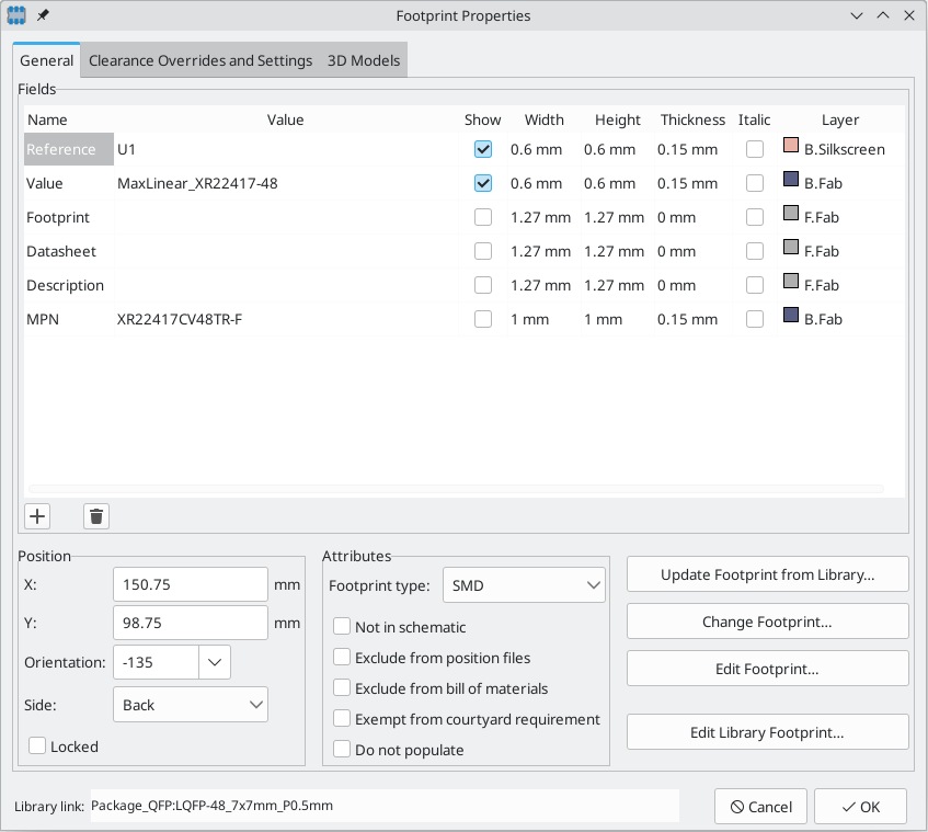
You can directly set a footprint’s exact absolute position, rotation angle, and PCB side using either the Footprint Properties dialog or the Properties panel.
To reposition a footprint relative to its current position, use the Move Exactly tool (Shift+M). The dialog lets you specify an X and Y translation, as well as a rotation, that will be applied to the footprint. The rotation can be performed relative to either the footprint’s anchor, the local coordinate origin, or the drill/place origin. You can also use polar coordinates instead of Cartesian coordinates.
To position a footprint relative to another object, you can use the Position Relative tool (Shift+P). With this tool, you select a reference point for the move and specify an offset. The footprint is moved to the specified offset relative to the reference point. The reference point can be one of the following:
-
The local origin, which is set to the cursor position when you press Space.
-
The grid origin, which is configured in the Grids dialog.
-
The location of an arbitrary item on the board, such as a specific pad in a footprint. After clicking the Select Item… button, click on the desired board item in the canvas to set the reference point.
-
An arbitrary point in the canvas. After clicking the Select Point… button, click at the desired location to set the reference point. You can use object snapping to select a specific point in an object, such as the end of a graphic line.
To position a footprint such that an arbitrary point in the footprint is positioned a certain distance from another arbitrary reference point, you can use the Position Interactively tool (right click a footprint → Positioning Tools → Position Interactively…).
This tool lets you interactively select two points that form the start and end of a position vector. The first point is a reference point in the footprint, and will move along with the footprint. The second point is a fixed reference that will remain stationary when the footprint is moved. The vector from the first point to the second point is shown graphically in the editing canvas. You can then give new X and Y (or polar) dimensions for the vector, which will move the footprint reference relative to the fixed reference such that the fixed reference is the specified distance from the footprint reference point. The dialog initially contains the vector dimensions before any move is performed, or in other words the initial distance between the footprint reference point to the fixed reference.
You can swap the position of two selected footprints using the Swap command (Alt+S). The first footprint is assigned the location, rotation, and board side of the second footprint, and vice versa. If there are more than two footprints selected, the locations are cycled: the last footprint gets the position of the first footprint, the first footprint gets the location of the second, and so on.
There are several convenience features that make it easier to find, select, and move specific footprints or footprints related to another footprint.
The Get and Move Footprint command (T) prompts you to choose a footprint from a list or by typing a reference designator. KiCad then attaches the chosen footprint to your cursor for a move operation.
There are two commands to select other footprints that need to be connected to the selected footprint but don’t yet have routed connections. The Select All Unconnected Footprints command (O) selects all footprints that have ratsnest lines to the currently selected footprints. The command can be executed repeatedly to further expand the selection based on the newly selected items. The Grab Nearest Unconnected Footprint command (Shift+O) selects the closest footprint with ratsnest lines to the currently selected footprint, and additionally begins to move it. If there are multiple footprints initially selected, the command will act like the Move Individually command described below, individually moving the closest unconnected footprint for each of the initially selected footprints.
You can select footprints based on their schematic sheet using the right click → Select → Items in Same Hierarchical Sheet command, which selects all other footprints that are in the same schematic sheet as the originally selected footprint.
If you want to move multiple selected footprints in sequence, use the Move Individually command (Ctrl+M). After triggering the command, KiCad will begin moving the first selected footprint. After you click to place the footprint, KiCad will immediately start moving the next footprint, in the same order that you selected the footprints. You can skip moving a footprint by pressing Tab, commit the current move and skip any remaining moves by double-clicking, or cancel all moves (including those already completed) by pressing Esc.
If you want to move a collection of footprints at once into one area, the Pack and Move Footprints command (P) closely packs the selected footprints together and moves them as a block.
| Move Individually and Pack and Move Footprints are useful in combination with other selection convenience features, such as cross-selection from the schematic or the advanced footprint selection features described above. For example, you could select a group of bypass capacitors in the Schematic Editor, switch to the PCB Editor where the corresponding footprints are now selected, and then use Move Individually to quickly place all of the bypass capacitor footprints close to their respective ICs. Alternatively, you could use one of the other selection tools, such as Select All Unconnected Footprints, to select many footprints from all over the board, then use Pack and Move Footprints to quickly put them all into a small area. |
Finally, KiCad can automatically place footprints onto the board. The auto-place function attempts to optimally place footprints to simplify ratsnest connections to other footprints. You can auto-place the selected footprints with Place → Auto-Place Footprints → Place Selected Footprints, or auto-place all footprints outside of the board outline with Place → Auto-Place Footprints → Place Off-Board Footprints.
Editing Footprints
Footprints in the board can be individually edited, both in terms of their properties (fields, attributes, clearance settings, etc.) and in terms of their physical pads and graphics. Editing a footprint in the board only affects that particular instance of the footprint; it does not affect any other copies of that footprint in the board, and it does not affect the library footprint.
To edit the properties of a footprint in the board, open its properties dialog (E)
The majority of the settings in this dialog are the same as in the footprint editor. You can edit the footprint’s fields, attributes, clearance and zone connection settings, 3D models, and embedded files, as in the footprint editor. However, here you can also set the footprint’s position, orientation, and side. You can also update the footprint from the library, exchange it for a different footprint, or edit the footprint itself in the footprint editor.
To edit the footprint’s physical form, i.e. its pads and graphics, you need to use the footprint editor. There are two buttons for opening a footprint in the editor, depending on whether you want to edit a single copy of a footprint in the board or a footprint’s source copy in the library.
-
Edit Footprint… will open the specific instance of the footprint in the footprint editor. Editing this footprint will only affect this one instance of the footprint in the board. It will not affect other instances of the footprint in the board, and it will not affect the library copy of the footprint. You can also open a board footprint in the footprint editor by right clicking the footprint in the board and selecting Open in footprint editor (Ctrl+E).
-
Edit Library Footprint… will open the library copy of the footprint in the footprint editor. Editing the library copy of the footprint will edit the footprint in the footprint library, but will not immediately affect any instances of that footprint in the board. To update footprints in the board with changes to the library footprint, use the Update Footprint from Library… tool. Editing the library footprint in this way is equivalent to opening the footprint editor, opening the appropriate footprint in its library, and editing it.
The Update Footprint from Library… button is used to update the board’s copy of the footprint to match the copy in the library. The Change Footprint… button is used to swap the current footprint to a different footprint in the library. These functions are described later.
Editing footprint fields
An individual symbol text field can be edited directly with the E hotkey (with a field selected instead of a footprint) or by double-clicking on the field.
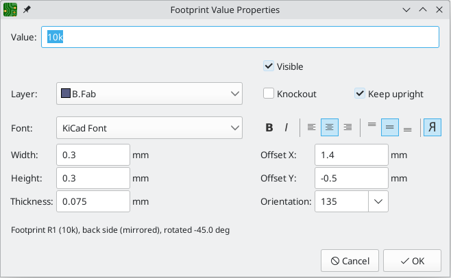
The options in this dialog are the same as those in the full Footprint Properties dialog, but are specific to a single field.
Only footprint fields can be edited this way in the board editor. Unlike fields, Footprint text is a graphic object that can only be edited or moved in the footprint editor.
| In versions of KiCad before version 8.0, footprint fields did not exist. Instead, footprint text could be edited directly in the board editor. In KiCad 8.0, footprint text is not editable in the board editor and can only be edited in the footprint editor. |
Updating and exchanging footprints
When a footprint is added to the board, KiCad embeds a copy of the library footprint in the board so that the board is independent of the system libraries. Footprints that have been added to the board are not automatically updated when the library changes. Library footprint changes are manually synced to the board so that the board does not change unexpectedly.
| You can use the Compare Footprint with Library tool to inspect the differences between a footprint in a board with its corresponding library footprint. |
To update footprints in the board to match the corresponding library footprint, use Tools → Update Footprints from Library…, or right click a footprint and select Update Footprint…. You can also access the tool from the footprint properties dialog.
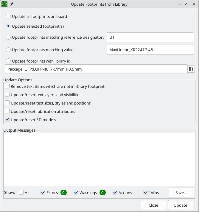
The top of the dialog has options to choose which footprints will be updated. You can update all footprints on the board, update only the selected footprints, or update only the footprints that match a specific reference designator, value, or library identifier. The reference designator and value fields support wildcards: * matches any number of any characters, including none, and ? matches any single character.
The middle of the dialog has options to control what parts of the footprint will be updated. You can select specific fields to update or not update, which properties of the fields to update (text content, visibility, size and style, and position), and how to handle fields that are missing or empty in the library footprint. You can also choose whether to update footprint attributes, such as footprint type, not in schematic, exclude from position files / bill of materials, exempt from courtyard requirement, and do not populate.
The bottom of the dialog displays messages describing the update actions that have been performed.
To change an existing footprint to a different footprint, use Edit → Change Footprints…, or right click an existing footprint and select Change Footprint…. This dialog is also accessible from the footprint properties dialog.
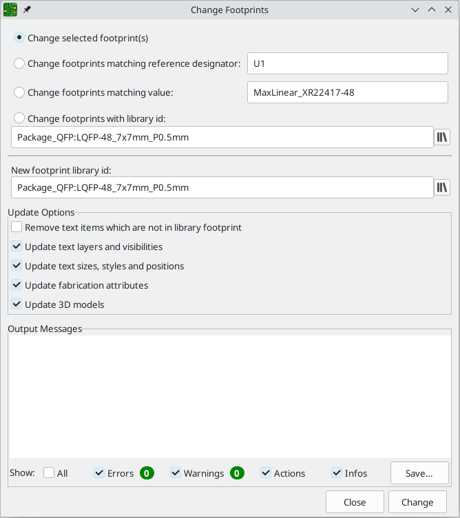
The options for the Change Footprints dialog are very similar to the Update Footprints from Library dialog.
Comparing footprints between board and library
When a footprint in a board diverges from the corresponding footprint in the original footprint library, you can use the Compare Footprint with Library tool to inspect the differences between the two versions of the footprint. Run the tool using Inspect → Compare Footprint With Library.
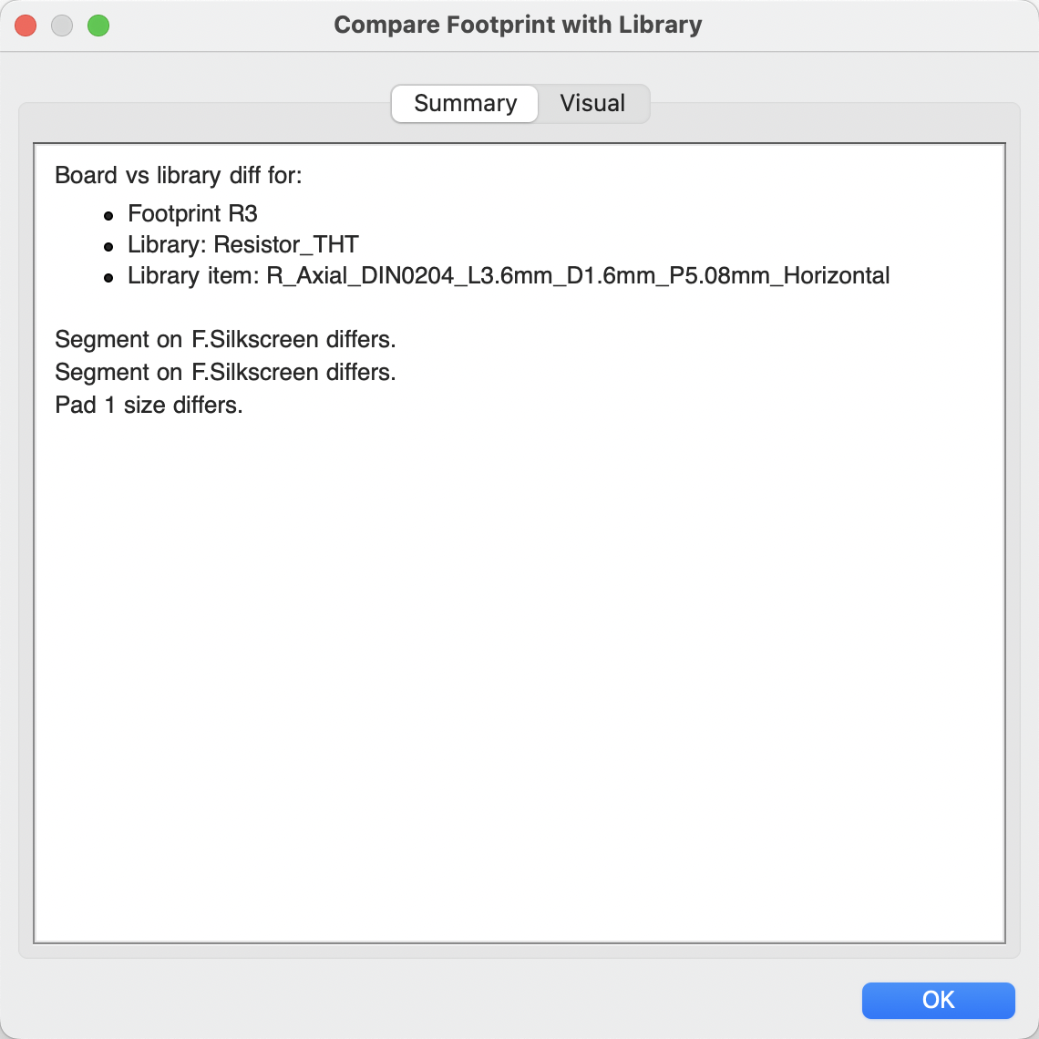
The Summary tab shows the name of the footprint, including its library and board reference designator, and provides a list of the differences between the board and library versions of the footprint.
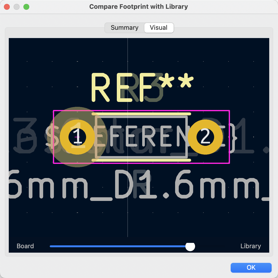
The Visual tab shows a visual comparison of the board and library versions of the footprint. This can be used as a visual diff tool.
By default, the comparison displays both versions of the footprint superimposed on each other. To see the changes more easily, you can drag the slider at the bottom of the tab to the right to emphasize the library version of the footprint in the superimposed view (making the board version of the footprint more transparent) or drag it to the left to emphasize the board version (making the library version more transparent). At the far right and left ends of the slider, the board and library versions of the footprint, respectively, are fully hidden. It may be helpful to drag the slider back and forth to see the changes more clearly.
You can press the A/B button, or use the / hotkey, to quickly toggle back and forth between the board and library versions.
The screenshot above shows a visual comparison with the board version of the footprint deemphasized. Looking at pad 1 on the left, you can see a large, partially transparent pad (from the board footprint) surrounding a fully opaque, smaller pad (from the library footprint). This indicates that the pad was enlarged in the board version of the footprint, or shrunk in the library version of the footprint.
使用焊盘
在将封装放置在电路板上之后,可以检查和编辑封装的每个单独的焊盘的属性。 换句话说,如果库中的封装设计不合适,就可以在电路板上封装的特定实例中覆盖单个封装焊盘的设计。 例如,你可能希望为一个需要在特定设计中保持不焊接的焊盘去除锡膏孔,或者你可能希望移动一个轴向引线电阻的通孔焊盘的位置,以适应特定的设计。
| 默认情况下,所有封装焊盘的位置都被锁定,因此可以编辑焊盘属性,但不能移动焊盘相对于封装其他部分的位置。 焊盘可以被解锁以允许自由移动,这对某些应用很有用(如具有不同引线位置的通孔封装),但通常不建议用于表面贴装封装。 |
当一个焊盘被选中时,焊盘属性对话框将通过上下文菜单或默认的快捷键 E 打开。 请注意,KiCad 认为如果你在焊盘附近点击,你可能是想选择整个封装而不是单个焊盘。 要选择单个焊盘,请确保在焊盘区域内点击,或者关闭选择过滤器中的 "封装" 设置(并确保 "焊盘" 设置打开),以防止意外地选择整个封装而不是特定的焊盘。
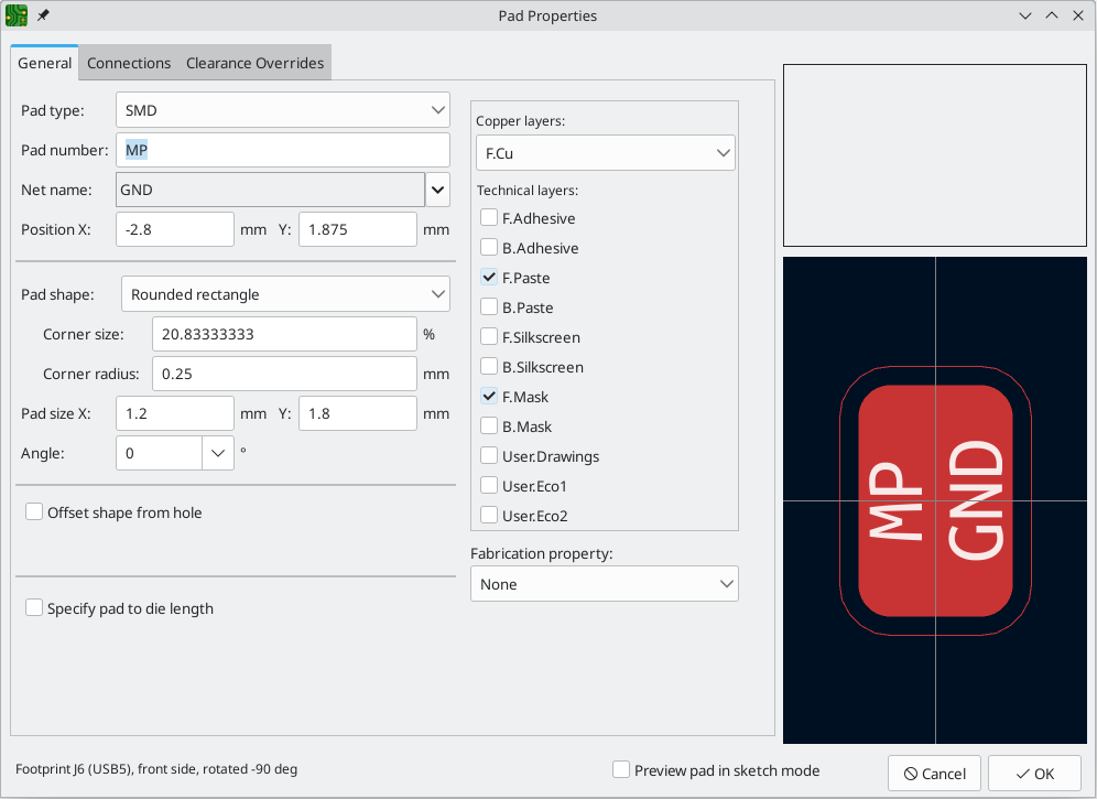
This dialog lets you edit the physical properties of the pad, including size and shape. You can also modify how the pad connects to other objects on the board, including clearance properties, teardrops, and thermal reliefs.
This dialog is the same as the pad properties dialog in the footprint editor, except that here you can also manually assign a net to a pad using the net name selector. The remaining options are explained in the Footprint Editor documentation.
| While you can manually assign nets to pads in the PCB editor, this is not a typical workflow. Usually net-to-pad connections are defined by the schematic and then transferred to the PCB editor. |
使用敷铜
敷铜区域,有时也被其他 EDA 工具称为铺铜或覆铜,是分配给一个特定网络的实心或网格状的铜箔区域,敷铜区域会自动保持与其他铜对象的间隙。 敷铜区域通常用于填充板层(或板层的一部分)上的所有自由空间,以创建接地和电源平面,承载大电流,或提供屏蔽。
| 一些 EDA 工具有单独的工具用于创建 "平面层" 及在信号层上创建敷铜区域。 在 KiCad 中,敷铜工具用于这两种应用。 |
区域是由一个多边形的 边框 来定义的,它定义了敷铜区域的最大范围。 这个边框并不代表实物铜,也不会出现在导出的制造数据中。 每次修改边框或边框内的任何对象时,必须 填充 该敷铜区域。 填充过程可以在单个敷铜区域上运行,也可以在电路板的所有区域上运行(默认快捷键 B)。 敷铜区域可以 不填充(默认快捷键 Ctrl+B),以提高性能并减少编辑大型电路板时的视觉混乱。
| By default, zone filling is a manual process rather than occurring every time an object changes that would result in a change to the zone copper. This is because zone filling can be a slow process on older computers or very large designs. It is important to make sure zone fills are up-to-date before generating outputs. KiCad will check that zones have been updated and warn you before generating outputs or running DRC when zones have not yet been refilled. You can optionally enable automatic zone-filling in the Preferences dialog (PCB Editor → Editing Options → Miscellaneous → Automatically refill zones). |
A zone fill occupies any unused space within the zone outline, automatically maintaining a specified clearance to board edges, holes, and copper objects on different nets. Zones do not fill outside of the board outline or within interior cutouts.
要绘制一个敷铜区域,请点击右侧工具栏的 “添加敷铜区域” 工具(![]() ),或者使用默认的快捷键 Ctrl+Shift+Z。 点击选择敷铜区域边框的第一个点。 敷铜区域属性对话框将出现,允许你选择敷铜区域的网络和其他属性。 这些属性可以在任何时候进行编辑,所以一开始正确选择它们并不是关键。 接受该对话框,继续放置点来定义敷铜区域的边框。 要完成这个区域,请双击来设置最后一个点。敷铜区域边框点可以像图形多边形一样进行修改,通过拖动方形手柄来移动一个角,或者拖动圆形手柄来移动一条边。 要编辑该敷铜区域的属性,请使用快捷键 E 或从上下文菜单中选择 “属性”。
),或者使用默认的快捷键 Ctrl+Shift+Z。 点击选择敷铜区域边框的第一个点。 敷铜区域属性对话框将出现,允许你选择敷铜区域的网络和其他属性。 这些属性可以在任何时候进行编辑,所以一开始正确选择它们并不是关键。 接受该对话框,继续放置点来定义敷铜区域的边框。 要完成这个区域,请双击来设置最后一个点。敷铜区域边框点可以像图形多边形一样进行修改,通过拖动方形手柄来移动一个角,或者拖动圆形手柄来移动一条边。 要编辑该敷铜区域的属性,请使用快捷键 E 或从上下文菜单中选择 “属性”。
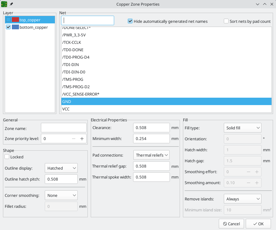
Layer: A single zone object can create filled copper on one or more copper layers. Check the box next to each copper layer that this zone outline should fill on. The copper on each layer will be filled independently, but all layers will share the same net.
Net: Select the electrical net that the zone copper should be connected to. It is possible to create zones with no net assignment. Zones with no net will keep clearance from any copper objects on any net.
Zone name can be used to assign a specific name to a zone. This name can be used to refer to the zone in custom DRC rules.
Zone priority level determines the order in which multiple zones on a single layer are filled. The highest priority level zone on a given layer will be filled first. Lower-priority zones will keep clearance to the filled areas of higher-priority zones. Two zones on the same layer with the same priority level will overlap (short-circuit) with each other, unless they are assigned different nets. When two zone outlines with the same priority and different nets touch, one zone will maintain clearance to the other so that they don’t short.
Locked controls whether or not the zone outline object is locked. Locked objects may not be manipulated or moved, and cannot be selected unless the Locked Items option is enabled in the Selection Filter panel.
Outline display controls how the zone outline is drawn on screen. In Line mode, only the border lines of the outline are drawn. In Hatched mode, hatch lines are drawn on the inside of the outline border for a short distance, to make the zone outline more apparent. In Fully Hatched mode, hatch lines are drawn across the entire inside of the zone outline.
Corner smoothing controls the behavior of the filled copper areas at corners of the outline. Corners can be smoothed by a chamfer or fillet, or can extend all the way to the outline corner if smoothing is disabled. The chamfer or fillet size is configurable when those modes are selected.
| 默认情况下,倒角和圆角不会被添加到区域边框的内角,因为这将导致填充的铜延伸到边框之外。 如果需要光滑的内角,请在电路板设置对话框的约束部分启用 允许敷铜区域边框外的圆角 选项。 |
Clearance controls the minimum clearance the filled areas of this zone will keep from other copper objects. Note that if two clearance values are in conflict, the larger clearance value will be used. For example, if a zone is set to use 0.2mm clearance but its netclass is set to use 0.3mm clearance, the result will be an 0.3mm clearance.
Minimum width controls the minimum size of narrow necks of copper created inside the zone. Any copper areas that would be below this minimum width are removed during the filling process.
Pad connection controls the way that the filled zone areas will connect to footprint pads on the same net. Solid connections will result in the copper completely overlapping the pads. Thermal reliefs will result in small copper spokes connecting the pad to the rest of the copper zone, increasing the thermal resistance between the pad and the rest of the zone. This can be useful for hand soldering. Reliefs for PTH will apply thermal reliefs to plated through-hole pads and use solid connections for surface mount pads. None will result in the zone not connecting to any pads on the same net.
Thermal relief gap controls the distance maintained between any pad and the copper zone when the pad connection mode is set to generate thermal reliefs.
Thermal spoke width controls the width of the "spokes", or short copper segments connecting the pad to the rest of the copper zone.
Fill type controls how the copper zone is filled: the default is solid fill, which will result in copper filling in all available space within the zone outline. The zone can also be set to fill a hatch pattern, which will fill the area with a pattern that contains less copper. This can be useful for flexible printed circuits and other specialty applications.
Orientation controls the angle of the hatch pattern lines. An orientation of 0 degrees will result in the hatch pattern using horizontal and vertical lines.
Hatch width controls the width of each line in the hatch pattern.
Hatch gap controls the distance between each line in the hatch pattern.
Smoothing effort controls the style of smoothing applied to the hatch pattern. A value of 0 will result in no smoothing, and a value of 3 will result in the finest smoothing. Higher values will result in longer processing time and larger Gerber files.
Smoothing amount is a ratio that controls the size of the smoothing chamfers or fillets that are generated when smoothing effort is set to a value other than 0. An amount of 0.0 results in no smoothing, and a value of 1.0 results in maximum smoothing (in other words, a chamfer or fillet equal to half of the hatch gap).
Remove islands controls the behavior of isolated copper areas, also called islands, after the initial zone fill. When this is set to always, isolated areas inside the zone are removed. When set to never, isolated areas are left alone, and will result in copper areas that are not connected to the rest of the net. When set to below area limit, a minimum island size can be specified, and islands below this threshold will be removed.
| 无论 移除死铜 设置如何,死铜都不会从没有电气连接的敷铜区域中移除。 换句话说,仅可以从具有至少一个电气连接的敷铜中移除死铜。 |
Managing zones
Instead of editing a single zone with the Zone Properties dialog, you can use the Zone Manager tool to you view, edit, and prioritize all zones in the board at once. To run the Zone Manager, click Tools → Zone Manager.
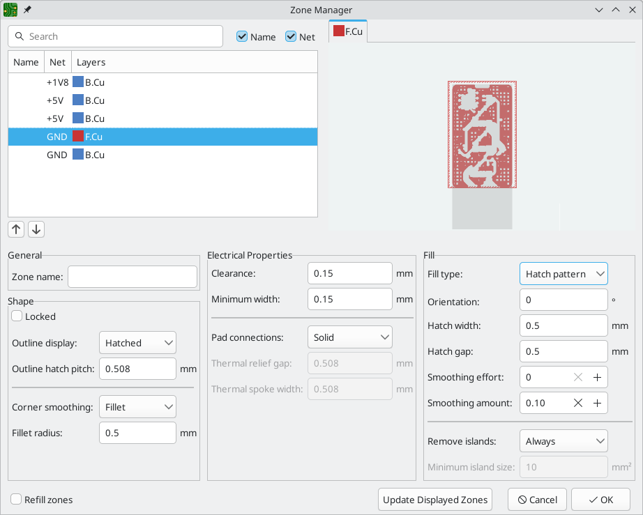
The top left of the dialog shows a list of all zones in the board, displaying the name (if any), net, and layers for each zone. The order of the zones in the list reflects the priority of each zone: higher priority zones are higher in the list. To change the priority of a zone, use the ![]() and
and ![]() buttons to move it up or down in the list. You can filter the list of zones by typing into the filter box. The filter matches against the zones' name and/or net, depending on which filter options are enabled.
buttons to move it up or down in the list. You can filter the list of zones by typing into the filter box. The filter matches against the zones' name and/or net, depending on which filter options are enabled.
Selecting a zone in the list shows a preview of that zone in the top right. If the selected zone spans multiple layers, each layer is shown individually. You can preview each layer by clicking the appropriate layer tab above the preview.
The bottom part of the dialog shows the settings for the selected zone, which are explained above. You can preview the new settings by clicking the Update Displayed Zones button, which updates the zone preview without affecting the board. Changing the properties of a zone in the Zone Manager will not update the board until you press OK. If the Refill zones option is enabled, all zones will be refilled when you accept the dialog. If Refill zones is not enabled, zones will not be refilled until you manually refill them.
布线
KiCad 具有交互式布线器的功能:
-
Allows manual or guided (semi-automatic) routing of single tracks and differential pairs
-
可通过以下方式修改现有设计:
-
拖动已有导线时进行重新布线
-
拖动封装时对连接到封装焊盘的导线进行重新布线
-
-
允许通过插入蛇形线
+来调整布线长度和差分对的偏移(相位) 为具有严格时序要求的设计调整布线形状
默认情况下,布线器在放置布线时遵循配置的设计规则:新布线的尺寸(宽度)将取自设计规则。在确定新布线和过孔的放置位置时,布线器将遵循设计规则中设置的铜间隙。 如果需要的话,可以通过使用高亮冲突布线器模式,或打开布线器设置中的 “允许 DRC 违规” 选项来禁用这种行为(见下文)。
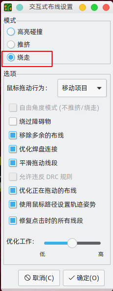
The router has three modes that can be selected at any time in the Interactive Router Settings dialog. The router mode is used for routing new tracks, but also when dragging existing tracks using the Drag (hotkey D) command. These modes are:
-
Highlight Collisions: in this mode, most of the router features are disabled and routing is fully manual. When routing, collisions (clearance violations) will be highlighted in green and the newly-routed tracks cannot be fixed in place if there is a collision unless the Allow DRC Violations option is turned on. In this mode, up to two track segments may be placed at a time (for example, one horizontal and one diagonal segment).
-
Shove: in this mode, the track being routed will walk around obstacles that cannot be moved (for example, pads and locked tracks/vias) and shove obstacles that can be moved out of the way. The router prevents DRC violations in this mode: if there is no way to route to the cursor position that does not violate DRC, no new tracks will be created.
-
Walk Around: in this mode, the router behaves the same as in Shove mode, except no obstacles will be moved out of the way.
Which mode to use is a matter of preference. For most users, we recommend using Shove mode for the most efficient routing experience or Walk Around mode if you do not want the router to modify tracks that are not being routed. Note that Shove and Walk Around modes always create horizontal, vertical, and 45-degree (H/V/45) track segments. If you need to route tracks with angles other than H/V/45, you must use Highlight Collisions mode and enable the Free Angle Mode option in the Interactive Router Settings dialog.
There are four main routing functions: Route Single Track, Route Differential Pair, Tune length of a single track, and Tune skew of a differential pair. All of these are present in both the Route menu dropdown (individually) on the top toolbar and the drawing toolbar in two overloaded icons on the drawing toolbar on the right. The use of the overloaded icons is described above. One is for the two Route functions and one is for the two Tune functions. In addition, the Route menu allows the selection of Set Layer Pair and Interactive Router Settings.
要进行布线布线,请点击布线 ![]() 图标(从绘图工具栏或从顶部工具栏 布线 菜单中)或使用快捷键 X。 点击一个起始位置,选择要布线的网络,并开始布线。 布线的网络会自动高亮显示,网络允许的间隙会在当前布线的周围用灰色的轮廓表示。 可以通过改变 "偏好设置" 对话框中的 "间隙轮廓" 设置来禁用间隙轮廓功能。
图标(从绘图工具栏或从顶部工具栏 布线 菜单中)或使用快捷键 X。 点击一个起始位置,选择要布线的网络,并开始布线。 布线的网络会自动高亮显示,网络允许的间隙会在当前布线的周围用灰色的轮廓表示。 可以通过改变 "偏好设置" 对话框中的 "间隙轮廓" 设置来禁用间隙轮廓功能。
| The clearance outline shows the maximum clearance from the routed net to any other copper on the current layer. It is possible to use custom design rules to specify different clearances for a net to different objects. These clearances will be respected by the router, but only the largest clearance value will be shown visually. |
当布线器处于活动状态时,将从布线起点到编辑器光标绘制新的线段。这些线段是未固定的临时 (unfixed temporary) 对象,它们显示当您左键鼠标或 Enter 键来确定布线 (fix the route) 时将创建哪些线段。非固定布线段以比固定布线段更亮的颜色显示。当您使用 Esc 键或通过选择另一个工具退出布线器时,将只保存固定布线段。完成布线操作(快捷键 End) 将固定所有布线并退出布线器。
在布线时,可以使用 "撤消上一个布线段" 命令 (快捷键 Backspace) 取消上一个固定的布线。您可以重复使用此命令后退已固定的布线。
In previous versions of KiCad, using the left mouse button or Enter to fix the routed segments would fix all segments up to but not including the segment ending at the mouse cursor location. In KiCad 6 and later, this behavior is optional, and by default, all segments including the one ending at the mouse cursor location will be fixed. The old behavior can be restored by disabling the "Fix all segments on click" option in the Interactive Router Settings dialog.
布线时,可以按住 Ctrl 键禁用网格捕捉,按住 Shift 键禁用对焊盘和过孔等对象的捕捉。
| 也可以通过更改偏好设置对话框的编辑选项部分中的磁吸点首选项来禁用对象的捕捉。 我们建议您在一般情况下保持启用对象捕捉,这样就不会意外地在焊盘或过孔上略微偏离中心结束布线。 |
交互式布线设置
The interactive router settings can be accessed through the Route menu, or by right-clicking on the ![]() button in the toolbar. These settings control the router behavior when routing tracks as well as when dragging existing tracks.
button in the toolbar. These settings control the router behavior when routing tracks as well as when dragging existing tracks.
| Setting | Description |
|---|---|
Mode |
Sets the operating mode of the router for creating new tracks and dragging existing tracks. See the routing overview for more information. |
Free angle mode |
Allows routing tracks at any angle, instead of just at 45-degree increments. This option is only available if the router mode is set to Highlight collisions. |
Allow DRC violations |
Allow placing tracks and vias that violate DRC rules. This option is only available if the router mode is set to Highlight collisions. |
Shove vias |
Allow the router to shove vias along with tracks. When this is disabled, vias cannot be shoved. This option is only available if the router mode is set to Shove. |
Jump over obstacles |
Allow the router to attempt to move colliding tracks behind solid obstacles (such as pads). This option is only available if the router mode is set to Shove. |
Remove redundant tracks |
Automatically removes loops created in the currently-routed track, keeping only the most recently routed section of the loop. |
Optimize pad connections |
When this setting is enabled, the router attempts to avoid acute angles and other undesirable routing when exiting pads and vias. |
Smooth dragged segments |
When dragging tracks, attempts to combine track segments together to minimize direction changes. |
Optimize entire track being dragged |
When enabled, dragging a track segment will result in KiCad optimizing the rest of the track that is visible on the screen. The optimization process removes unnecessary corners, avoids acute angles, and generally tries to find the shortest path for the track. When disabled, no optimizations are performed to the track outside of the immediate section being dragged. |
Use mouse path to set track posture |
Attempts to pick the track posture based on the mouse path from the routing start location. |
Fix all segments on click |
When enabled, clicking while routing will fix the position of all the track segments that have been routed, including the segment that ends at the mouse cursor. A new segment will be started from the mouse cursor location. When disabled, the last segment (the one that ends at the mouse cursor) will not be fixed in place and can be adjusted by further mouse movement. |
布线形态
在水平(H) / 垂直 (V) / 45 度模式下布线时,形态 是指一组两个线段如何连接单个 H/V/45 度线段无法到达的两个点。 在这种情况下,这些点将由一条水平或垂直线段和一条斜线段 (45度) 连接。形态指的是这些线段的顺序:是水平/垂直线段在前还是斜线段在前。


KiCad 的布线器会尝试根据一系列因素自动选择最佳形态。一般说来,布线器会尝试最大限度地减少路线中的拐角数量,并尽可能避免 "槽糕" 的拐角 (如锐角)。当从焊盘布线或布线到焊盘时,KiCad 将选择使路线与焊盘最长边缘对齐的形态。
在某些情况下,KiCad 无法正确猜测您想要的形态。要在布线时切换布线的形态,请使用切换布线形态命令 (快捷键 /)。
In situations where there is no obvious "best" posture (for example, when starting a route from a via), KiCad will use the movement of your mouse cursor to select the posture. If you would like the route to begin with a straight (horizontal or vertical) segment, move the mouse away from the starting location in a mostly horizontal or vertical direction. If you would like the route to begin diagonally, move in a diagonal direction. Once the cursor is a sufficient distance away from the routing start location, the posture is set and will no longer change unless the cursor is brought back to the starting location. Detection of posture from the movement of the mouse cursor can be disabled in the Interactive Router Settings dialog as described below.
| 如果使用切换布线形态(Switch Track Posture)命令覆盖 KiCad 选择的形态,则在当前布线操作的剩余部分中,将禁用鼠标移动姿势的自动检测。 |
布线转角模式
KiCad’s router can place tracks using four different corner modes:
-
45 degree (default)
-
45 degree rounded
-
90 degree
-
90 degree rounded
Use the Track Corner Mode command (Ctrl+/) to cycle between these modes. These corner modes do not apply when the router is in free angle mode.
In the 45 degree modes, tracks can be placed horizontally, vertically, or at 45 degree diagonals, and track segments are joined at 45 or 135 degree angles. This is the most common corner mode and it is selected by default.

45 degree track corner mode
In the 90 degree modes, diagonal tracks cannot be placed and track segments are joined at 90 degree angles.

90 degree track corner mode
When routing with rounded corners, each routing step will place either a straight segment, a single arc, or both a straight segment and an arc. The track posture determines whether the arc or the straight segment will be placed first.

45 degree rounded track corner mode

90 degree rounded track corner mode
Track corners can also be rounded after routing by using the Fillet Tracks command after selecting the tracks on either side of the corner to be filleted. If a contiguous track selection contains multiple corners, they will all be filleted.
| Dragging of tracks with arcs is not supported. Arcs are treated as immovable by the shove router. |
布线宽度
The width of the track being routed is determined in one of three ways: if the routing start point is the end of an existing track and the ![]() button on the top toolbar is enabled, the width will be set to the width of the existing track. Otherwise, if the track width dropdown in the top toolbar is set to "use netclass width", the width will be taken from the netclass of the net being routed (or from any custom design rules that specify a different width for the net, such as inside a neckdown area). Finally, if the track width dropdown is set to one of the pre-defined track sizes configured in the Board Setup dialog, this width will be used.
button on the top toolbar is enabled, the width will be set to the width of the existing track. Otherwise, if the track width dropdown in the top toolbar is set to "use netclass width", the width will be taken from the netclass of the net being routed (or from any custom design rules that specify a different width for the net, such as inside a neckdown area). Finally, if the track width dropdown is set to one of the pre-defined track sizes configured in the Board Setup dialog, this width will be used.
| 布线宽度永远不能小于在电路板设置对话框的约束部分中配置的最小布线宽度。如果添加的预定义宽度低于此最小约束,则将使用最小约束值。 |
KiCad 的布线器支持活动布线过程中的布线宽度调整。 换句话说,要改变导线中间的宽度,必须结束布线,然后从上一个布线的末端重新开始一条新的布线。 要改变活动布线的宽度,可使用快捷键 W 和 Shift+W,切换在电路板设置对话框中配置的布线宽度。
放置过孔
在进行布线时,切换层会在当前(未固定)导线的末端插入一个过孔。 一旦你放置了过孔,布线将继续在新层上进行。 有几种方法可以选择一个新层并插入过孔:
-
使用快捷键选择特定的图层,如 PgUp 选择
F.Cu或 PgDn 选择B.Cu。 -
By using the Next Layer or Previous Layer hotkeys (+ and -).
-
By using the Place Via hotkey (V), which will switch to the next layer in the active layer pair.
-
通过使用 "选择图层并放置通孔过孔" 操作(快捷键 <),将打开一个对话框来选择目标层。
After using any of the above methods to add a via and change layer, but before clicking to fix the via and commit the current track segment, you can cancel placing the via by pressing V. The via will be removed and routing will continue on the original layer.
You can place a via and end the current track, without changing layers, by pressing V and then double-clicking to place the via.
过孔的尺寸将取自当前的 “过孔尺寸” 设置中,可通过顶部工具栏的下拉列表或使用快捷键 (') “增加过孔尺寸” 及快捷键 (\) “减小过孔尺寸” 。与布线宽度类似,当过孔大小设置为"使用网络类尺寸" 时,将使用 "电路板设置" 的 "网络类" 部分中配置的过孔大小 (除非被自定义设计规则覆盖)。
You can also place microvias and blind/buried vias while routing. Use the hotkey Ctrl+V to place a microvia and Alt+Shift+V to place a blind/buried via. While regular vias always go through every board layer, microvias and blind/buried vias can start and end on any layer, not just the outer layers.
| For the purposes of DRC, microvias are not considered drilled holes as they are laser drilled rather than mechanically drilled. See the DRC documentation for more information. |
布线器放置的过孔被认为是已布线导线的一部分。 这意味着过孔网络可以自动更新(就像导线网络一样),例如,当从原理图中更新 PCB 时改变了导线的网络名。 在某些情况下,这可能是不需要的,例如在创建缝合孔时。 对于特定的过孔,可以通过关闭过孔属性对话框中的 "自动更新过孔网络" 复选框来禁用过孔网络的自动更新。 使用 "添加独立过孔" 工具放置的过孔在创建时禁用这一设置。
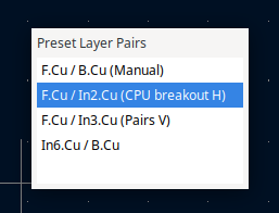
Layer Pairs
The active layer is swapped with the other one in the current layer pair using the Place Via hotkey (V).
You can define the active pair along with a list of "preset" layer pairs in the Set Layer Pair dialog, accessed from the two-color swatch on the toolbar. These pairs are stored in the project file.
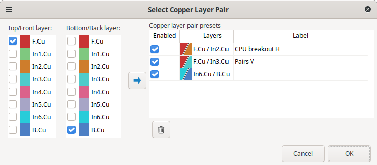
Each can be enabled or disabled, and given an optional user-friendly name.
The enabled presets can be cycled using the Cycle Layer Pair Presets hotkey (Shift+V). If the last-used or current layer pair is not a preset, it is included in the list with the name "Manual".
Placing free vias
In addition to placing vias while routing, you can also place standalone vias. These vias connect to items that they touch when they are placed. Free vias may be useful for via stitching, via shielding, thermal design, or other reasons.
To place a free via, click the ![]() button or press Ctrl+Shift+X, then click in the desired location in the editing canvas. If you place a via directly over a track, it will connect to that track as if it was placed while routing: it will take the track’s net, it will create a joint in the track, and dragging the via will also drag the attached tracks.
button or press Ctrl+Shift+X, then click in the desired location in the editing canvas. If you place a via directly over a track, it will connect to that track as if it was placed while routing: it will take the track’s net, it will create a joint in the track, and dragging the via will also drag the attached tracks.
The net assigned to a free via depends on where the via was placed. If the via was placed over a track or pad, it will have the same net as the track, and its Automatically update via nets setting will be enabled so that its net changes with the track’s net. Otherwise, the via will take the net of any zone under the via, if one exists, and its net will not update automatically. If there are multiple zones under the via, you will be prompted to choose which net to use. If there is no zone, the via will not have a net assigned.
修改布线
布线完成后,可以通过移动或拖动来修改它们,或者删除并重新布线。 当选择一个导线时,快捷键 U 可以用来将选择范围扩大到所有连接的导线。 第一次按下 U 将选择与焊盘或过孔最近的连接点之间的导线。 第二次按 U 将再次扩大选择范围,包括所有层上与所选导线相连的所有导线。 用这种技术选择导线可以用来快速删除整个布线网络。
There are two different drag commands that can be used to reposition a track segment. The Drag (45-degree mode) command, hotkey D, is used to drag tracks using the router. If the router mode is set to Shove, dragging with this command will shove nearby tracks. If the router mode is set to Walk Around, dragging with this command will walk around or stop at obstacles. Multiple tracks can be dragged at once using this command. The Drag Free Angle command, hotkey G, is used to split a track segment into two and drag the new corner to any location. Drag Free Angle behaves like the Highlight Collisions router mode: obstacles will not be avoided or shoved, only highlighted.
| 目前还不能拖动包含圆弧的布线。在某些情况下,尝试拖动这些布线会导致圆弧被删除。可以通过选中特定圆弧并使用拖动命令 (D) 来调整其大小。使用此命令调整圆弧大小时,不执行 DRC 检查。 |
移动命令(快捷键 M)也可以在导线上使用。 该命令将拾取选定的导线,而忽略任何未被选中的附加导线或过孔。 使用移动命令移动导线时,不会进行 DRC 检查。
It is also possible to move a footprint while keeping tracks attached to the footprint as it moves. To do so, use the drag command (D) with one or more footprints selected. Any tracks that end at one of the footprint’s pads will be dragged along with the footprints. This feature has some limitations: it only operates in Highlight Collisions mode, so the tracks attached to footprints will not walk around obstacles or shove nearby tracks out of the way. Any DRC violations caused by the drag operation will be highlighted and will be prevent the footprint drag from being committed when you click. To ignore the violations and commit the drag anyway, use Ctrl+click. Additionally, only tracks that end at the origin of the footprint’s pads will be dragged. Tracks that simply pass through the pad or that end on the pad at a location other than the origin will not be dragged.
To break a single track segment into two, use the Break tool (right click a track → Break Track). The track will be broken into two connected track segments at the cursor location. Each track segment can then be selected, moved, and edited individually. To recombine the segments into a single segment, drag the drack, or use the merge co-linear tracks option in the Cleanup Tracks and Vias dialog.
Editing track and via properties
You can modify the width of tracks and the size of vias, without re-routing them, in the properties dialog for the track or via. This modifies all selected tracks and vias. The properties dialog shows the relevant properties for the items in the selection: if both tracks and vias are selected, then properties for both types of objects will be displayed, but if only one type of object is selected then properties for the other type of object will not be shown.
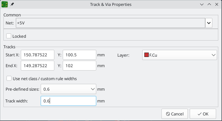
In the Common section, you can change the assigned net of the selected objects using the Net dropdown. If the Automatically update via nets option is checked, the selected vias cannot have their assigned net manually changed, but instead will be assigned the net of any zone or pad that they touch. You can also lock the selected objects.
In the Tracks section, you can set the start and end position of the tracks and the layer they are on. You can also change the track width, either from a list of pre-defined sizes or to an arbitrary value.
You can remove the solder mask from on top of tracks on outer layers by enabling the Solder mask checkbox. When enabled, solder mask openings will be drawn for each of the selected tracks with the same shape as the source track. The Expansion textbox controls the size of the mask opening relative to the original track: the expansion value will be added to each side of the original track to form the mask shape. For example, a 1mm wide track with a 1mm expansion would result in a 3mm wide mask cutout, because the 1mm expansion is added to both sides of the track.
In the Vias section you can change the properties of selected vias. You can change the position of a via, the via’s type (through, micro, or blind/buried), and which layers it spans. Through vias always start and end on the front and back copper layers, but micro vias and blind/buried vias can start and end ony any layers.
You can modify the via annulus and hole diameters, either from a list of pre-defined sizes or to arbitrary values. A via’s diameter and hole size can be defined on a per-layer basis. This is also known as defining the via’s padstack. The Padstack mode controls whether the via shape is the same on all layers or whether individual layers are individually controlled.
-
In the Normal padstack mode, the via’s diameter and hole size are the same on all layers.
-
In the Front/Inner/Back padstack mode, the via’s diameter and hole size can be controlled separately for the front layer, the back layer, and the inner layers (the inner layers will have identical settings). The Edit layer dropdown controls which layer (or group of layers) is currently being displayed and edited.
-
In the Custom padstack mode, the via’s diameter and hole size can be controlled completely independently on each layer. The Edit layer dropdown controls which layer is currently being displayed and edited.
The Annular rings setting controls which layers will have annular rings for the via.
-
When set to All copper layers, the via will have annular rings on every layer.
-
When set to Start, end, and connected layers, the via will have annular rings on its start and end layers as well as any layer with a track or zone connection to the via. Any layer without track or zone connections, other than the start and end layers, will not have an annular ring.
-
When set to Connected layers only, the via will have annular rings only on layers with a track or zone connection to the via. Any layer without track or zone connections will not have an annular ring.
Annular rings can be removed or added in bulk using the Edit Track and Via Properties dialog or by running the Unused Pads tool.
The Front tenting and Back Tenting options control whether the via has front and back solder mask covering it.
-
When set to From design rules, the tenting settings are taken from the Solder Mask/Paste panel in Board Setup.
-
When set to Tented, the via will be covered in solder mask, regardless of the settings in Board Setup.
-
When set to Not tented, the via will not be covered with solder mask, regardless of the settings in Board Setup.
If the ![]() button is pressed, the front and rear tenting settings will be linked. If it is unpressed, they can be modified independently.
button is pressed, the front and rear tenting settings will be linked. If it is unpressed, they can be modified independently.
You can also change the teardrop properties for vias in this dialog.
| The properties of selected tracks and vias can also be modified using the Properties Manager. |
Bulk editing tracks and vias
To modify tracks and vias in bulk you can use the Edit Track and Via Properties dialog (Edit → Edit Track & Via Properties…)..
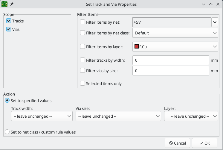
Scope settings restrict the tool to editing only tracks, vias, or both. If no scopes are selected, nothing will be edited.
Filter Items restricts the tool to editing particular objects in the selected scope.
Objects will only be modified if they match all enabled and relevant filters
(some filters do not apply to certain types of objects. For example, via size
filters do not apply to tracks). If no filters are enabled, all objects in the
selected scope will be modified. For filters with a text box, wildcards are
supported: * matches any characters, and ? matches any single character.
-
Filter items by net filters to items assigned the specified net.
-
Filter items by netclass filters to items assigned to the specified netclass.
-
Filter items by layer filters to items on the specified board layer.
-
Filter tracks by width filters to tracks with the specified track width.
-
Filter vias by size filters to vias with the specified track width.
-
Selected items only filters to the current selection.
Properties for filtered objects can be set to new values in the bottom part of the dialog. Properties can be set to arbitrary values by selecting set to specified values or set to the default value from the net class (or custom rule) by selecting set to net class / custom rule values.
When setting to specified values, you can choose -- leave unchanged -- to preserve objects' existing values, or select a new value from the dropdown menu. For Track width and Via size, the options are the pre-defined track or via sizes from Board Setup.
Removing unused pads
You can quickly remove unused annular rings from pads and vias using the Unused Pads tool (Tools → Remove Unused Pads…). This will leave annular rings in place on layers where they are used and remove them on layers where they are not used. An annular ring is considered unused if there are no track or zone connections to the pad/via on that layer.
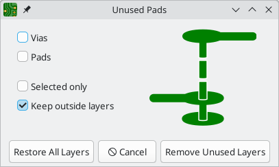
The Remove Unused Layers button removes all unused annular rings from pads and vias that meet the selected filter settings. The Restore All Layers button restores all annular rings to the pads and vias that meet the selected filter settings.
The checkboxes filter which objects will be modified (annular rings removed or restored) and which layers will be removed for those objects.
-
If the Vias checkbox is enabled, annular rings for vias will be modified.
-
If the Pads checkbox is enabled, annular rings for pads will be modified.
-
If the Selected only checkbox is enabled, only selected vias and pads will have their annular rings modified. If it is disabled, annular rings for all vias and pads will be modified. This setting applies in combination with the Vias and Pads checkboxes; for example, a selected via will not be modified if the Via checkbox is disabled.
-
If the Keep outside layers checkbox is enabled, the pad or via’s start and end layers will remain, even if they are unused.
Cleaning up tracks and vias
There is a dedicated tool for performing common cleanup operations on tracks and vias, which is run via Tools → Cleanup Tracks & Vias….
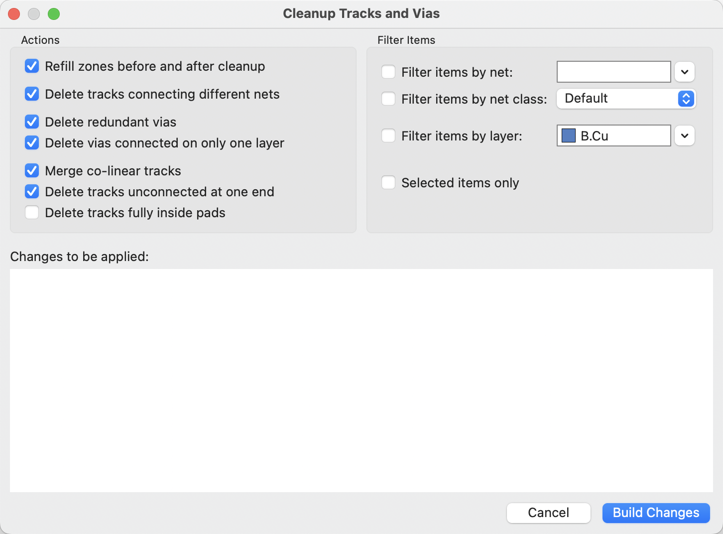
The following cleanup actions are available and will be performed when selected:
-
Refill zones before and after cleanup: refills all zones both before and after the cleanup operation. If unchecked, zone fills will not be changed.
-
Delete tracks connecting different nets: removes any track segments that short multiple nets.
-
Delete redundant vias: remove vias that are redundant because they are located on top of another via or on top of a through hole pad.
-
Delete vias connected on only one layer: removes vias that are only connected to copper on a single layer and are therefore unnecessary.
-
Merge co-linear tracks: merges any track segments that are connected and co-linear into a single equivalent track segment.
-
Delete tracks unconnected at one end: removes track segments that have at least one dangling end.
-
Delete tracks fully inside pads: removes tracks that have both start and end points within a pad and are therefore unnecessary.
You can also filter the objects that will be cleaned up by net, netclass, layer, or selection.
-
Filter items by net: limits the cleanup to tracks and vias assigned to the specified net.
-
Filter items by netclass: limits the cleanup to tracks and vias in the specified netclass.
-
Filter items by layer: limits the cleanup to tracks and vias on the specified layer.
-
Selected items only: limits the cleanup to just the selected tracks and vias.
Any changes that will be applied to the board are displayed at the bottom of the dialog after clicking the Build Changes button. After building the changes, the button changes to say Update PCB. The changes are not applied until you press the Update PCB button.
Routing Convenience Functions
KiCad offers several functions to make certain routing operations more convenient.
If you need to route a number of tracks from a set of pads, you can use the Route Selected tool to quickly route from each pad in sequence. Select the pads you want to use as starting points, then right click and choose Route Selected (Shift+X) to route from each pad in sequence. The router will begin a track from the first selected pad, which you can route as you would any other track. When you complete the track, the router will automatically begin a new track from the next pad in the selection, in the same order that you selected the pads. Pads that already have tracks attached are skipped. You can also skip routing the current track and move on to the next pad by pressing Esc. You can also select footprints instead of pads; all unrouted pads in the selected footprints will be used as starting points.
If you want to route a number of tracks to a set of pads, instead of from the pads, you can use the Route Selected From Other End tool. Select the pads you want to use as ending points, then right click and choose Route Selected From Other End (Shift+E). This tool works the same way as the Route Selected tool, except it uses each selected pad as an end point rather than a starting point. The starting point for each track is the other end of the ratsnest line for each selected pad.
Routing from the other end is also possible while routing individual tracks: press Ctrl+E while routing a track to commit the current segment and begin routing from the other end of the in-progress track’s ratsnest line.
Finally, you can quickly unroute tracks connected to an object (footprint, pad, or track) by selecting the object, right-clicking, and choosing Unroute Selected. Any tracks connected to the selected object will be removed, starting at the selected object and continuing until another pad is encountered.
Automatically completing tracks
KiCad’s router can automatically route individual tracks, based on the connections defined in the schematic. This can be thought of as a limited form of auto-routing that considers a single track at a time. The router will only use the current layer; it will not use vias or change layers.
While routing, press the F key to have the router attempt to automatically finish the current track. The track will be automatically routed from the end of the last fixed track segment to the closest ratsnest anchor. If the router can’t automatically finish the track, it will allow you to complete the track manually. This action can also be performed by clicking Attempt Finish in the context menu while routing.
When the router is not the active tool, you can automatically route multiple tracks by selecting footprints, pads, and tracks to route from, right clicking, and choosing Attempt Finish Selected (Autoroute) (Shift+F). You do not need to select both ends of a desired connection; the router will route from the selected item to its nearest ratsnest anchor. If multiple items were selected, each item will be routed in sequence, in the order that they were selected. If a connection cannot be automatically completed, the tool will pause with the router active so that you can complete the track manually. With the automatic completion paused for a manual connection, you can press Esc to skip routing the current track. After manually completing the track or skipping the connection, the tool will continue attempting to route the remaining connections.
差分对布线
Differential pairs in KiCad are defined as nets with a common base name and a positive and negative suffix. KiCad supports using + and -, or P and N as the suffix. For example, the nets USB+ and USB- form a differential pair, as do the nets USB_P and USB_N. In the first example, the base name is USB, and USB_ in the second. The suffix styles cannot be mixed: the nets USB+ and USB_N do not form a differential pair. Make sure you name your differential pair nets accordingly in the schematic in order to allow use of the differential pair router in the PCB editor.
要对差分对进行布线,请点击差分对布线 ![]() 图标(从绘图工具栏或从顶部工具栏 布线 下)或使用快捷键 6。 点击一个焊盘、过孔或现有差分对线段的末端,开始布线。 你可以从差分对的正网络或负网络开始布线。
图标(从绘图工具栏或从顶部工具栏 布线 下)或使用快捷键 6。 点击一个焊盘、过孔或现有差分对线段的末端,开始布线。 你可以从差分对的正网络或负网络开始布线。
差分对布线器将尝试用设计规则中的间隙规则进行布线(差分对间隙可以在电路板设置对话框的 “网络类” 部分中配置,也可以通过使用自定义设计规则来配置)。如果布线的起始或结束位置与配置的间隙不同,布线器将创建一个较短的 "扇出" 部分,以最大限度地缩短差分对未耦合的布线长度。
当切换层或使用 放置过孔 (V) 操作时,差分对布线器将创建两个相邻的过孔。这些过孔将被放置在尽可能靠近彼此的位置,同时遵守铜的间隙规则以及孔到孔的间隙规则。
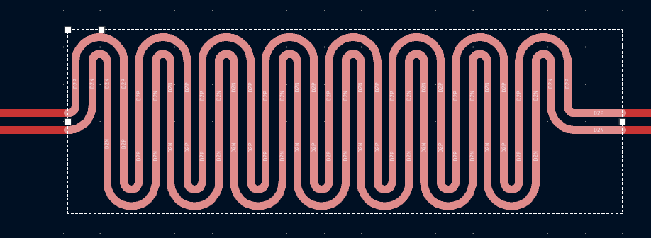
长度调整
The length tuning tools can be used to add serpentine tuning shapes to tracks after routing. Length tuning shapes are persistent objects that can be modified after they are created. To tune the length of a track, first pick the appropriate tool.
-
The single-track length tuning tool (icon
 or hotkey 7) will add serpentine shapes to bring the length of a single track up to the target value.
 -
The differential pair length tuning tool (icon
 or hotkey 8) will do the same for a differential pair.
 -
The differential pair skew tuning tool (icon
 or hotkey 9) will add length to the shorter member of a differential pair in order to eliminate skew (phase difference) between the positive and negative sides of the pair.
As with the Routing icons, the Tuning icons are found in both the Route menu dropdown from the top toolbar and the drawing toolbar on the right.
When a tuning tool is active, you can hover over tracks in the board to show a status window that displays their current length or skew as well as the target values. Click on the desired track to start tuning it. As you move the mouse cursor along the track, meander shapes will be added interactively. If a target length has been set, meanders will stop being added when the target length is reached. You can set a target length with custom DRC rules or in the tuning shape properties; both methods are explained below. The popup window next to the cursor shows a live measure of the length or skew compared to the design targets. You can adjust the spacing (1 to increase and 2 to decrease) and amplitude (3 to increase and 4 to decrease) while you tune. When you are done, click again to commit the tuned shape. The tuned track doesn’t need to be perfect because you can adjust the shape after committing it. You can also place multiple tuning shapes on the same track.
| The length tuning tools only support tuning the length of point-to-point nets between two pads. Tuning the length of nets with different topologies is not supported. |
| Differential pair length tuning can only be applied to the coupled portions of differential pairs. To apply length tuning to the uncoupled portions of differential pairs, you must use single-track length tuner. |
Editing tuning patterns
After a tuning pattern has been added, it can be selected, modified, and moved. While it is selected, the target length and routed length are shown in the message panel at the bottom left of the window.
When a pattern is selected, editing handles appear, which let you adjust the pattern geometry.
-
Dragging the handles at the ends of the pattern will expand or contract the pattern along the track.
-
Dragging the corner handle towards or away from the track will respectively decrease or increase the maximum meander amplitude.
-
The final handle controls the meander spacing; dragging it towards the corner handle will increase the spacing, while dragging it away from the corner handle will increase the spacing.
The selection box and editing handles represent the maximum allowable extents of the tuning pattern. Making the box smaller will reduce the size of the tuning pattern, even if this results in the tuned track being shorter than the target length. When the box is enlarged, the tuning pattern will expand to fill the box until the target length is reached.
You can move a tuning pattern along its track by selecting it and dragging with the mouse, or using the Move tool (M). Deleting a tuning pattern (Del) removes the tuning pattern and restores the original untuned tracks. You can also ungroup the tuning pattern, which will decompose it into its component tracks. The basic tracks have the same shape as the tuning pattern but can be edited individually. Once ungrouped into tracks, a tuning pattern cannot be regrouped.
Another way to edit a tuning pattern is through its properties dialog. The properties dialog exposes several additional parameters that can’t be modified using the on-canvas interactive editor. These properties can also be edited in the Properties Manager.
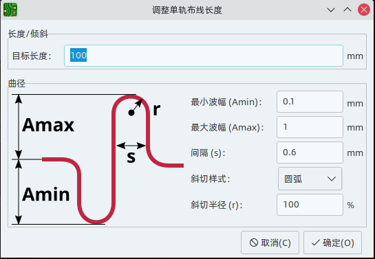
As with the interactive editor, you can set a maximum amplitude for the tuning pattern and a spacing between meanders, but here you can set a minimum amplitude and configure the corner style. Corners can be filleted (rounded) or chamfered. In each case you can set the radius as a percentage of the maximum possible radius for the spacing and amplitude. You can also configure the tuning pattern to be single-sided, which restricts it to one side of the baseline, as opposed to the default style which positions meanders on both sides of the baseline.
You can set default values for these properties in the Design Rules → Length-tuning Patterns page of the Board Setup dialog. Each type of tuning pattern (single track length, differential pair length, and differential pair skew) can have its own defaults.
Finally, the tuning pattern properties dialog is one of two ways to set the target length or skew for a tuning pattern. Setting length targets is explained below.
Setting target length and skew
There are two ways to set a target length or skew for a net:
-
In the properties dialog for a tuning pattern that has already been added to a track.
-
Using a custom DRC rule with the
lengthand/orskewconstraints.
The first method is to specify a target in the target length or target skew field of the tuning pattern’s properties dialog. This target will only apply to the selected tuning pattern. Therefore, length targets set in this way must be set separately for each tuning pattern in the design. The properties dialog for a tuning pattern is only accessible after the pattern is initially created, so changing a target length or skew in this way may require the pattern to be adjusted to meet the new target value, if the pattern’s geometric constraints do not allow sufficient space to meet the new target.
You can also set a target length and/or skew using custom design rules. If custom rules are used, they will override any targets set in tuning pattern properties, unless the override custom rules checkbox is enabled in the tuning pattern properties.
Using a custom rule allows you to set a net’s target length and/or skew up front, before a pattern is created. With custom rules you can set different length and skew targets based on specific criteria, such as netclass or net name. You will also result in a DRC violation if the net’s length or skew is out of bounds.
When target length or skew is adjusted in a custom DRC rule after a pattern is created, the pattern geometry will not be automatically updated to achieve the new target. You can use Edit → Update All Tuning Patterns to recalculate all tuning patterns to meet the new targets.
The following example custom rule sets a target length and skew for nets in the high_speed netclass. The target length is 100mm, and a DRC error will be raised if it is below 95mm or above 105mm. The target skew is at most 0.1mm.
(rule "target length and skew"
      (condition "A.hasNetclass('high_speed')")
      (constraint length (min 95mm) (opt 100mm) (max 105mm))
      (constraint skew (max 0.1mm)))
See the custom rule documentation for more details of how to create rules that only apply to certain nets.
Length tuning pitfalls and tips
The length tuner only tunes nets with a point-to-point topology; branching nets are not supported. When the length tuner encounters a branch, it stops at the branch and only considers the length of the net up to that branch.
Sometimes you may end up with leftover stub tracks somewhere in your design. These can turn what appears to be a point-to-point net into a branched topology, which will prevent length tuning from working as expected. It may be easier to find such stub tracks when you switch footprints, vias, and tracks to outline mode (![]() ,
, ![]() , and
, and ![]() buttons, respectively). You can also use the track cleanup tool (Tools → Cleanup Tracks and Vias…) to remove many of these stubs automatically.
buttons, respectively). You can also use the track cleanup tool (Tools → Cleanup Tracks and Vias…) to remove many of these stubs automatically.
By default, the length tuner includes vias in its length calculations. Only the layer-to-layer length of the via is used, which may be shorter than the full top-to-bottom via height if the tuned path is not exclusively on the board top and bottom. The accuracy of this calculation depends on the board stackup being accurately configured. Via length can be ignored in length tuner calculations by deselecting include stackup height in track length calculations in the Constraints page of the Board Setup dialog.
The length tuner is optimized for adjusting the effective electrical distance between two points, and therefore it calculates net length in a slightly different way than other tools, such as the Net Inspector. In addition to discounting net branches and unused portions of vias, the length tuner also optimizes paths through pads to use the shortest possible path in its calculations. In comparison, the Net Inspector reports a simple summation of copper segment lengths. Both calculations are accurate, but they are optimized for different purposes. These differences are discussed in more detail in the Net Inspector documentation.
Teardrops
Teardrops are areas of extra copper that smooth the transition between tracks and pads, vias, or other tracks with different width. Teardrops are added to increase the mechanical robustness of a track connection. They also reduce the risk of a misaligned drill hole disconnecting a track from a drilled pad or via.
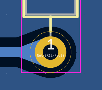
There are two ways to add teardrops to your design. You can add them in bulk using the Edit Teardrops dialog, or you can add them to individual pads and vias in the respective properties of the pad or via.
Adding teardrops in bulk
The Edit Teardrops dialog (Edit → Edit Teardrops…) lets you add teardrops to many board objects at once. The dialog has controls for filtering which objects are affected and settings for configuring the shape of the new teardrops. It also lets you edit or remove existing teardrops.
The Scope section controls which types of objects will be affected: PTH pads, SMD pads, vias, and/or track-to-track connections. The Filter Items section lets you filter objects by other criteria; you can filter items by net, net class, and layer, or choose to act only on round pads, pre-existing teardrops, or the objects in your selection.
The Action section controls whether to add or remove teardrops, as well as the size and shape of the new teardrops.
Remove Teardrops will remove teardrops that match the scope and filtering options at the top of the dialog. Remove All Teardrops will remove all teardrops on the board, even if they do not match the scope and filters.
Add teardrops with default values for shape will add teardrops with the configured default teardrop settings to every board object that matches the scope and filters. To configure the default teardrop settings, click the Edit default values in Board Setup link or manually open the Teardrops panel in Board Setup. The defaults are configured separately for teardrops connecting to round shapes, rectangular shapes, or between tracks.
Instead of using the default values, you can provide custom teardrop settings by selecting Add teardrops with specified values. The available teardrop settings are:
-
Prefer zone connection: if selected, a teardrop will not be created if the object is also connected to a zone.
-
Allow teardrops to span 2 track segments: if selected, the teardrop will be able to spread over a second track segment if the first segment is too short to support a full teardrop.
-
Maximum track width: a teardrop will not be created for a track connection that is wider than this percentage of the pad width (minimum pad dimension).
-
Best length: the ideal length of the teardrop, as a percentage of the width (smallest dimension) of the attached object.
-
Maximum length: the maximum length of the teardrop, as an absolute length.
-
Best width: the ideal width of the teardrop, as a percentage of the width (smallest dimension) of the attached object.
-
Maximum width: the maximum width of the teardrop, as an absolute width.
-
Curved edges: if selected, the teardrop edges will be curved instead of a straight line.
Adding a teardrop to an object that already has a teardrop will update the existing teardrop with the new settings. However, you can leave any existing teardrop setting in an object unchanged by setting the value to -- leave unchanged -- in a textbox, or by selecting the third, indeterminate state for a checkbox. Any value set this way will not be updated in the targeted objects' teardrop settings.
Adding teardrops to individual objects
Rather than in bulk, you can add or edit teardrops for individual vias in the properties dialog for that via, or for individual pads in the Connections tab of the pad’s properties dialog. The settings in the properties dialogs are the same as in the Edit Teardrops dialog. You can also edit teardrops for individual pads and vias with the Properties Manager.
Other details about teardrops
Teardrops in KiCad are small zones, meaning that when they refill they avoid shorting to copper objects on other nets. They are initially filled when they are added, but they are unfilled and refilled with other zones on the board: when using the Unfill All Zones and Refill All Zones commands, running DRC, generating fabrication outputs, etc. Teardrops can be shown in filled or outline mode using the zone display controls in the left toolbar.
Teardrops can be added to any type of pad, including custom pads. Some custom pad shapes may produce undesirable teardrop shapes. In those cases, it may be preferable to disable teardrop generation for those specific pads.
Graphics and text
Graphical objects (lines, arcs, rectangles, circles, polygons, text, tables, and dimensions) can exist on any layer. They exist primarily for aesthetics and documentation, although shapes on copper layers can make electrical connections and have nets assigned.
Graphical shapes
Graphical shapes are geometric objects that can be drawn on any board layer.
When they are drawn on copper layers, graphical objects can be assigned nets and make connections to other copper objects, much like tracks and zones. There are differences between copper shapes and tracks or zones, however:
-
The shape of a graphical object is exactly defined by its own properties (size, position, line width, fill, etc.) and is not affected by other nearby objects. In contrast, a zone fills the area within a specified outline, but avoids different-net copper items to automatically maintain a specified clearance.
-
Graphic lines and arcs are edited as simple shapes; the interactive router is not used for drawing or modifying them. Therefore collisions with other items are not detected interactively as they would be when routing tracks (although they will be detected by DRC).
The buttons on the right toolbar can be used to create:
-
Lines (
 , default hotkey Ctrl+Shift+L)
 -
Arcs (
 , default hotkey Ctrl+Shift+A)
 -
Bezier curves (
 , default hotkey Ctrl+Shift+B)
 -
Rectangles (
 )
) -
Circles (
 , default hotkey Ctrl+Shift+C)
 -
Polygons (
 , default hotkey Ctrl+Shift+P)
To place a shape, select the tool, then click in the canvas to place the shape’s first point. Click again to place the shape’s second point. For rectangles and circles, placing the second point will fully define the shape and finish drawing it. Some shapes require three or more points to be placed, however. Arcs require three points, while lines, polygons and bezier curves can accept an arbitrary number of points, and require a double click to complete.
To modify an existing graphical object, select it, then drag its editing handles to change the shape. Moving a handle at the vertex of a shape will move that vertex. Moving a handle on the edge of a shape will move that edge while maintaining the edge’s angle.
Arcs have two vertex editing modes, which are selectable in Preferences → PCB Editor → Editing Options or by right clicking the ![]() button on the right toolbar.
button on the right toolbar.
-
The first mode (keep arc center, adjust radius) maintains the position of the arc center as as the arc endpoints or midpoint are dragged, changing the radius as necessary.
-
The second mode (keep arc endpoints or direction of starting point) maintains the position of the arc endpoints and the arc’s direction of curvature as the midpoint or center are dragged.
Just like with tracks, you can expand a selection from one graphic line to include all other contiguous graphic lines by pressing U.
The properties of a graphic shape can be adjusted in the shape’s properties dialog or with the Properties Manager.
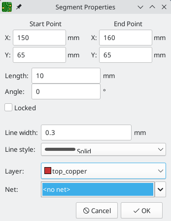
-
The top section contains controls for editing the object’s location and shape. Some types of objects can be edited in multiple ways, with each method in its own tab. For example, a line segment can be edited by its start and end points, by its start point, length, and angle, or by its start and mid points.
-
Locked controls whether or not the text object is locked. Locked objects may not be manipulated or moved, and cannot be selected unless the Locked Items option is enabled in the Selection Filter panel.
-
Closed shapes (rectangles, circles, and polygons) can be outlines or filled shapes, which is controlled by the Filled shape checkbox.
-
The Line width option controls the width of the outline, even for filled objects. The outline width extends on both sides of the "ideal" shape of the graphic object. For example, a graphic circle that is defined to have 2mm radius and 0.2mm line width will consist of a torus with an outer radius of 2.1mm and inner radius of 1.9mm. If the shape is filled and the line width is set to 0, the shape will be a filled circle with 2mm radius. Several line styles are available in the Line style dropdown: solid, dashed, dotted, dash-dot, and dash-dot-dot.
| You can customize the default style of newly-created graphical shapes in the Text & Graphics Defaults section of the Board Setup dialog. |
-
The Layer dropdown controls which layer the shape is placed on. Graphical shapes on copper layers can have a net assigned in their properties dialog. Copper shapes with a net make connections like tracks or zones. Unlike zones, copper graphical objects always maintain their shape and do not keep clearance to other copper objects.
-
When shapes are placed on outer copper layers, they can be configured to affect the corresponding solder mask layer in addition to their primary copper layer by enabling the Solder mask checkbox. When enabled, a shape on the front copper layer will also be drawn on the front solder mask layer, while a back copper shape will also be drawn on the back solder mask layer. Because solder mask layers are negative, this will result in a solder mask opening with the same shape as the copper shape. The Expansion textbox controls the size of the mask opening relative to the original copper shape: the expansion value will be added to each side of the original shape to form the mask shape. For example, a 1mm wide copper segment with a 1mm expansion would result in a 3mm wide mask cutout, because the 1mm expansion is added to both sides of the segment.
Shape modification tools
KiCad has several tools for modifying combinations of graphic shapes in useful ways, such as chamfering two lines or combining two polygons. These tools are used by selecting the shapes you want to modify, right clicking, and then choosing the relevant tool in the Shape Modification submenu. Different tools are available for different combinations of selected shapes.
-
Heal shapes fixes a discontinuity between two lines or arcs. A new line segment is added to connect the ends of each shape together, up to a specified tolerance.
-
Fillet lines adds an arc to round the corner between two connected lines with a specified radius. The two original lines are shortened to meet the endpoints of the arc.
-
Chamfer lines adds a line segment to create a new edge between two connected lines with a specified setback. The two original lines are shortened to meet the endpoints of the new segment.
-
Dogbone corners adds circular reliefs to the corners of the selected shapes. This is similar to filleting, but the modified shape is larger than the original, with the added arcs intersecting the vertices of the original corners. In other words, the added reliefs exactly enclose the original corners. This can be useful for relieving the corners of interior cutouts so that they can be manufactured using a round cutting tool. Because dogbones are intended to allow interior corners to be manufactured, a dogbone is only added to a corner if the corner points into the body of the board as defined by the board outline. There is an option to Add slots to acute corners, which adds extended slots in corners that are too narrow to reach with a cutting tool of the selected radius.
-
Extend lines to meet lengthens two selected lines until they intersect each other. The two lines will share a coincident endpoint.
-
Merge polygons combines two or more selected polygons into one new polygon that is the union of the original shapes.
-
Subtract polygons subtracts one or more polygons from another polygon, resulting in a new polygon that is the difference of the original shapes. The first-selected polygon(s) are subtracted from the last-selected polygon.
-
Intersect polygons results in a new polygon that is the shape of the overlapping area between two or more selected polygons.
Converting objects to and from graphic shapes
KiCad provides tools to convert graphic objects to other types of objects, other types of objects to graphic objects, and graphic objects to other kinds of graphic objects. These tools are used by selecting the shapes you want to convert, right clicking, and then choosing the desired result object from the Create From Selection submenu. Most types of object conversions have several conversion options that are presented in a settings dialog. The exact options differ based on the target object type.
When converting to a graphic polygon, rule area, or zone, there are several options for how to convert the source objects into a polygonal outline.
-
If copy line width of first object is selected, an unfilled polygon will be created that has its line width taken from the line width of the first selected source object. This option is only available when converting to a graphic polygon, and the source object must be a closed shape.
-
If use centerlines is selected, an object with zero line width will be created, with its outline placed at the centerlines of the source objects. The source object must be a closed shape. If the target object is a graphic polygon, it will be filled.
-
If create bounding hull is selected, an object will be created with the specified line width. The object’s outline will be offset from the outermost extents of the source object by the specified gap. The source object does not need to be a closed shape when a bounding hull is created.
Most conversions provide a delete source objects after conversion option, which will result in the original object being deleted during the conversion, only leaving the new object in place. If this option is not selected, the conversion will leave the original object in place in addition to the new object. The original object will be selected following the conversion so that it can be manually deleted by pressing Delete.
The following conversion types are available:
-
Create Polygon From Selection converts a graphic shape, text, zone, rule area, or track into a polygon. This can be used to convert separate graphic shapes, such as lines and arcs, into a unified shape. It can also be used to convert a text object into a shape that can have its outline manipulated graphically.
-
Create Zone From Selection converts a graphic shape, text, zone, rule area, or track into a zone. In addition to the conversion settings, the conversion dialog also shows options for configuring the resulting zone. This can be used to create zone outlines with complex shapes, such as curves, that would otherwise be difficult to create using the zone tool.
-
Create Rule Area From Selection converts a graphic shape, text, zone, rule area, or track into a rule area. In addition to the conversion settings, the conversion dialog also shows options for configuring the resulting rule area. This can be used to create rule area outlines with complex shapes, such as curves, that would otherwise be difficult to create using the rule area tool.
-
Create Lines From Selection converts a graphic polygon or rectangle into graphic lines that follow the source shape’s outline. This can be used to convert a unified shape into its constituent outline segments.
-
Create Outsets From Selection converts the selected object (graphic shapes, pads, etc.) into a rectangle that surrounds the original shape with some spacing. This can be used to quickly create outlines, courtyards, etc., especially in combination with other shape modification tools.
-
The Outset distance specifies the minimum distance between the outset and the original shape. There will always be at least this much space between the two shapes.
-
If Round corners (when possible) is enabled, the outset will have rounded corners rather than being a simple rectangle.
-
If Round outwards to grid multiples (when possible) is enabled, the outset will be placed on the specified grid, rounding outwards when necessary so that the specified outset distance is maintained.
-
If Copy item layers is enabled, the outset will be drawn on the same layer as the original shape. If disabled, the outset will be drawn on the layer selected in the dropdown menu.
-
If Copy item thickness (when possible) is enabled, the outset will be drawn with the original item’s thickness if that item has a thickness, or the specified thickness otherwise. Some source items, like pads, do not have a thickness property. The specified thickness will always be used when this option is disabled.
-
-
Create Tracks From Selection converts a graphic shape, zone, or rule area into tracks that follow the source shape’s outline. If the source object is not on a copper layer, a dialog will be presented to specify the target copper layer. The source object is not removed following conversion, but remains selected so that it can be easily deleted if desired.
-
Create Arc From Selection converts a graphic line segment or track segment into a graphic arc. The arc’s endpoints are placed at the endpoints of the source segment and its thickness is taken from the source object’s line thickness. The source segment is not removed following conversion, but remains selected so that it can be easily deleted if desired.
Importing vector graphics
You can add graphic shapes from an external vector graphics file by importing the file into KiCad. DXF and SVG files are supported. To import the file, use File → Import → Graphics… (Ctrl+Shift+F).
Imported vector graphics are part of the design like any other graphic shape. In other words, they have an assigned board layer, they are included in fabrication outputs, and shapes on copper layers can make electrical connections.
The Import Vector Graphics File dialog has several options:
-
File specifies the vector graphics file to import.
-
Import Scale sets the scale factor for the import.
-
DXF default line width sets the line width for any items in a DXF file that do not specify a line width. It has no effect when not importing DXF files.
-
DXF default units sets the default unit for DXF files with unspecified units. It has no effect when not importing DXF files.
-
If Place At is enabled, the imported shapes are placed at the specified location, relative to the PCB Editor’s page origin. If it is disabled, the imported shapes are placed interactively.
-
If Layer is enabled, the imported shapes are placed onto the selected layer. If it is disabled, the shapes are placed onto the active layer.
-
If Group imported items is enabled, all shapes imported from the vector graphics file are added to a group.
-
If Fix discontinuities is enabled, any shape discontinuities smaller than the specified tolerance are filled by extending each segment until they intersect or adding an additional segment.
Text objects
Graphical text may be placed by using the ![]() button in the right toolbar or by keyboard shortcut Ctrl+Shift+T. Activating the tool brings up a text properties dialog. After configuring the text and its properties and accepting the dialog, you can click in the canvas to place the text.
button in the right toolbar or by keyboard shortcut Ctrl+Shift+T. Activating the tool brings up a text properties dialog. After configuring the text and its properties and accepting the dialog, you can click in the canvas to place the text.
You can also add text boxes, which are similar to regular text except that they have an optional border and they automatically reflow text within that border. Text boxes are placed with the ![]() button, and require clicking twice to specify the top left and bottom right corners of the box.
button, and require clicking twice to specify the top left and bottom right corners of the box.
-
Locked controls whether or not the text object is locked. Locked objects may not be manipulated or moved, and cannot be selected unless the Locked Items option is enabled in the Selection Filter panel.
-
Layer controls the text’s layer. Text may be placed on any layer, but note that text on copper layers cannot be associated with a net and cannot form connections to tracks or pads. Copper zones will fill around the rectangular bounding box of text objects.
-
There are several formatting options: text can be bolded, italicized, left/right/center aligned, top/bottom/center aligned, and reversed.
-
The knockout option adds a solid rectangle surrounding the text and makes the text itself a negative cutout. This feature is only available for regular text objects, not text boxes.
-
The Font dropdown lets you select a font for the text. You can use any TTF font available on your system, or the built-in KiCad stroke font.
| User fonts are not embedded by default in the project. If the project is opened on another computer that does not have the selected font installed, a different font will be substituted. You can optionally embed into the board file any fonts used by the design in the Embedded Files section of Board Setup. For maximum compatibility without embedding, use the KiCad font. Also consider converting text objects to polygons before sharing a project (right click a text object → Create from Selection → Create Polygon from Selection…). Text converted to polygons is not editable as text, but will render identically on any computer. |
-
You can adjust the text size with the text width and text height controls. When you are using the KiCad font, you can also adjust the stroke width with the thickness control. The Update Thickness According to Text Size button automatically sets the text thickness according to the text size: the thickness for normal text is set to the size divided by 8, and the thickness for bold text is set to the size divided by 5.
-
Position X and position Y control the text object’s location. These properties are not available for text boxes.
-
Orientation is the rotation angle of the text object. You can select an angle in 90 degree increments from the dropdown, or type in an arbitrary angle.
Text boxes additionally have options controlling their border.
-
The border checkbox makes the border visible or invisible. For visible borders, you can adjust the border’s thickness with the border width control and the line style with the border style control (solid, dashed, dotted, dash-dot, or dash-dot-dot).
-
The margins between the border and the text on each side of a text box can be set using the Properties Manager. Margins cannot be set in the Text Box Properties dialog.
| You can customize the default style of newly-created text objects in the Text & Graphics Defaults section of the Board Setup dialog. |
Finally, text supports markup for superscripts, subscripts, overbars, evaluating project variables, and accessing symbol field values.
| Feature | Markup Syntax | Result |
|---|---|---|
Superscript |
|
textsuperscript |
Subscript |
|
textsubscript |
Overbar |
|
text |
|
variable_value |
|
|
field_value of symbol refdes |
Tables
You can use a table to organize text in a tabular format. Tables have customizable borders, cell sizes, and headers, and can be placed on any layer.
To place a table, use the ![]() button in the right toolbar. Click in the canvas to place the top left corner of the table, then click again to place the bottom right corner of the table and finish drawing the table. The bigger you draw the table, the more rows and columns will be added by default, but rows and columns can be added or deleted after the table is created.
button in the right toolbar. Click in the canvas to place the top left corner of the table, then click again to place the bottom right corner of the table and finish drawing the table. The bigger you draw the table, the more rows and columns will be added by default, but rows and columns can be added or deleted after the table is created.
Editing table properties
When you finish drawing a table, the Table Properties dialog appears. You can also open the Table Properties dialog in several other ways:
-
Select any cell in the table, right click, and select Edit Table (Ctrl + E)
-
Select the entire table, right click, and select Properties… (E). You can select the entire table with a drag selection or by selecting a single cell, then right clicking and selecting Select Table.
-
Click the Edit Table… button in the Table Cell Properties dialog.
This dialog lets you edit the properties of the entire table, including the text in each cell and the separators between cells. To change the formatting of text in a cell, edit the properties of individual cells, instead of the properties for the entire table.
| The properties for a table can also be edited in the Properties Manager when the entire table is selected. |
The left side of the dialog displays an editable grid of the entire table. You can edit the contents of any cell by clicking on the cell in the grid. You can also edit the text in a cell by selecting the cell and using the Properties Manager.
| Text in table cells supports the markup described in the text objects section (superscripts, subscripts, strikethroughs, etc.). |
The right side of the dialog contains formatting options for the table.
-
The Layer dropdown controls which board layer the table is on.
-
The Locked checkbox controls whether or not the table is locked. Locked objects may not be manipulated or moved, and cannot be selected unless the Locked Items option is enabled in the Selection Filter panel.
-
The External border and Header border checkboxes control whether there is a border drawn around the entire table and the cells in the top row, respectively. When Header border is enabled, the border below the cells in the top row is styled using these external border settings rather than the row/column line settings. The line width of the header borders is controlled by the Width field. The line style can be set to solid, dashed, dotted, dash-dot, or dash-dot-dot using the Style dropdown menu.
-
The Row Lines and Column lines checkboxes enable horizontal lines between rows and vertical lines between columns, respectively. These have the same formatting options as the external and header borders.
Editing table cell properties
Instead of editing the properties of an entire table, you can also edit the properties of individual cells. This modifies selected cells, but does not affect other cells. To open the Table Cell Properties dialog, double click on a cell, or select a cell, right click, and choose Properties… (E). If you select multiple cells, the properties dialog will act on all of them at once.
| You can select multiple cells by clicking and dragging. |
| To select all cells in a row or column, select a cell in that row or column, right click, and choose Select Row(s) or Select Column(s). You can select multiple rows or columns in this way by starting with multiple cells selected. |
This dialog contains formatting options for the text in each cell.
-
Horizontal alignment and Vertical alignment control how text is positioned within the cell.
-
Font controls the text font used in the cell.
-
The Bold and Italic checkboxes bold and italicize the text, respectively. These are three-state checkboxes, which can be set to off, on, or no change. No change is useful when multiple cells with different bold/italic settings are being edited at the same time.
-
The Text width, Text height, and Thickness control the size and thickness of the text. Thickness only has an effect when the font is set to the KiCad Font.
-
The Cell margins textboxes control the amount of spacing around the top, bottom, left, and right of the text in the cell.
You can click the Edit Table… button to open the properties dialog for the entire table.
| The properties for a table cell can also be edited in the Properties Manager when one or more table cells is selected. |
Editing table layout
The layout of a table (size and number of columns and rows) is initially set when you create a table, but you can also edit the layout after creation.
To resize a row or column, select a cell in that row or column, then drag the handle on the right (to change the column width) or the bottom (to change the row height) to the desired size.
To add rows or columns, select a cell next to where the new row or column should go, right click, then choose Add Row Above, Add Row Below, Add Column Before, or Add Column After, as desired.
To delete rows or columns, select a cell in the row or column you want to delete, then right click and choose Delete Row(s) or Delete Column(s). To delete multiple rows or columns, start with a selection that spans all the rows or columns you want to delete.
You can merge multiple cells into a single cell by selecting all the cells you want to merge, right clicking, and choosing Merge Cells. To unmerge them, select the merged cell, right click, and choose Unmerge Cells.
尺寸标注
尺寸标注是用于显示测量值或电路板设计上的其他标记的图形对象。 它们可以被添加到任何绘图层中,但通常被添加到某个用户层。 KiCad 目前支持五种不同类型的标注:对齐、正交、中心、径向和引线。
-
Aligned dimensions (
 ) show a measurement of
distance between two points. The measurement axis is the line that connects those two points, and
the dimension graphics are kept parallel to that axis.
) show a measurement of
distance between two points. The measurement axis is the line that connects those two points, and
the dimension graphics are kept parallel to that axis. -
Orthogonal dimensions (
 ) also measure the
distance between two points, but the measurement axis is either the X or Y axis. In other words,
these dimensions show the horizontal or vertical component of the distance between two points.
When creating orthogonal dimensions, you can select which axis to use as the measurement axis based
on where you place the dimension after selecting the two points to measure.
) also measure the
distance between two points, but the measurement axis is either the X or Y axis. In other words,
these dimensions show the horizontal or vertical component of the distance between two points.
When creating orthogonal dimensions, you can select which axis to use as the measurement axis based
on where you place the dimension after selecting the two points to measure. -
Center dimensions (
 ) create a cross mark to
indicate a point or the center of a circle or arc.
) create a cross mark to
indicate a point or the center of a circle or arc. -
Radial dimensions (
 ) show a measurement between
a center point and the outside of a circle or arc. The center point is indicated by a cross.
) show a measurement between
a center point and the outside of a circle or arc. The center point is indicated by a cross. -
Leader dimensions (
 ) create an arrow with a leader line
connected to a text field. This text field can contain any text, and an optional circular or
rectangular frame around the text. This type of dimension is often used to call attention to parts
of the design for reference in fabrication notes.
) create an arrow with a leader line
connected to a text field. This text field can contain any text, and an optional circular or
rectangular frame around the text. This type of dimension is often used to call attention to parts
of the design for reference in fabrication notes.
创建一个尺寸标注后,可以编辑其属性(快捷键 E)以改变显示数字的格式以及文本和图形线的风格。
| You can customize the default style of newly-created dimension objects in the Text & Graphics Defaults section of the Board Setup dialog. |
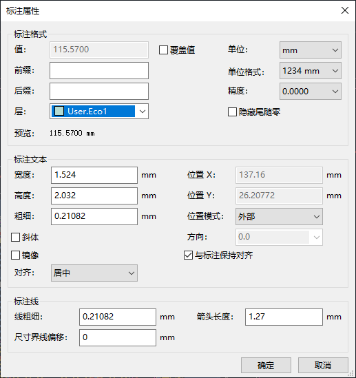
尺寸标注格式选项
-
Override value: When enabled, you may enter a measurement value directly into the Value field that will be used instead of the actual measured value.
-
Prefix: Any text entered here will be shown before the measurement value.
-
Suffix: Any text entered here will be shown after the measurement value.
-
Layer: Selects which layer the dimension object exists on.
-
Units: Selects which units to display the measured value in. Automatic units will result in the dimension units changing when the display units of the board editor are changed.
-
Units format: Select from several built-in styles of unit display.
-
Precision: Select how many digits of precision to display.
-
Arrow direction: Select whether the dimension object’s arrow(s) point inwards towards the value text or outwards away from the text. The arrow direction can also be set while drawing a dimension by right clicking and selecting Switch Dimension Arrows.
-
Suppress trailing zeroes: Select whether to hide trailing zeroes in the value text.
尺寸标注文本选项
大多数尺寸标注文本选项与其他图形文本对象的选项相同(见上面的图形对象部分)。 也有一些特殊的选项适用于尺寸标注文本:
-
Position mode: Choose whether to position the dimension text manually, or to automatically keep it aligned with the dimension measurement lines.
-
Keep aligned with dimension: When enabled, the orientation of the dimension text will be adjusted automatically to keep the text parallel with the measurement axis.
尺寸标注线选项
-
Line thickness: Sets the thickness of the graphical lines that make up a dimension’s shape.
-
Arrow length: Sets the length of the arrow segments of the dimension’s shape. A negative arrow length reverses the arrow direction.
-
Extension line offset: Sets the distance from the measurement point to the start of the extension lines.
-
Extension line overshoot: Sets the distance from the dimension’s line to the end of the extension lines.
引线选项
Leader dimensions have unique options:
-
Value: Enter the text to show at the end of the leader line.
-
Text frame: Select the desired border around the text (circle, rectangle, or none).
批量编辑文本和图形
Properties of text and graphics, including footprint fields and dimensions, can be edited in bulk using the Edit Text and Graphics Properties dialog (Edit → Edit Text & Graphic Properties…).
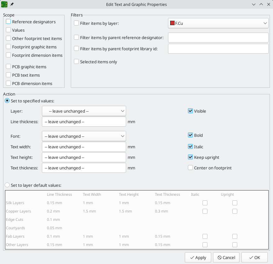
范围和筛选器
Scope settings restrict the tool to editing only certain types of objects. If no scopes are selected, nothing will be edited.
Filters restrict the tool to editing particular objects in the selected scope.
Objects will only be modified if they match all enabled and relevant filters
(some filters do not apply to certain types of objects. For example, parent
footprint filters do not apply to graphic items and are ignored for the purpose
of changing graphic properties). If no filters are enabled, all objects in the
selected scope will be modified. For filters with a text box, wildcards are
supported: * matches any characters, and ? matches any single character.
-
By layer filters to items on the specified board layer.
-
By parent reference designator filters to fields in the footprint with the specified reference designator.
-
By parent footprint library link filters to fields in footprint with the specified library link (library and footprint name).
-
Selected items only filters to the current selection.
操作
被筛选对象的属性可以在对话框的底部设置为新的值。通过选择 设置为指定值,可以将属性设置为任意值,或者通过选择 设置为图层默认值,将属性重置为其图层的默认值。
下拉列表和文本框可以被设置为 --保持不变-- 以保留现有值。复选框可以被选中或不被选中,以启用或禁用某个变化,但也可以切换到第三种 "保持不变" 状态。
-
所有项目都可以设置其 层。
-
图形对象可以修改其 线的粗细。
-
Text properties that can be modified are font, text width, text height, text thickness (KiCad font only), emphasis (bold and italic), orientation (keep upright), and alignment (center on footprint). Footprint fields can also have their visibility set.
Cleaning up graphics
There is a dedicated tool for performing common cleanup operations on graphics, which is run via Tools → Cleanup Graphics….
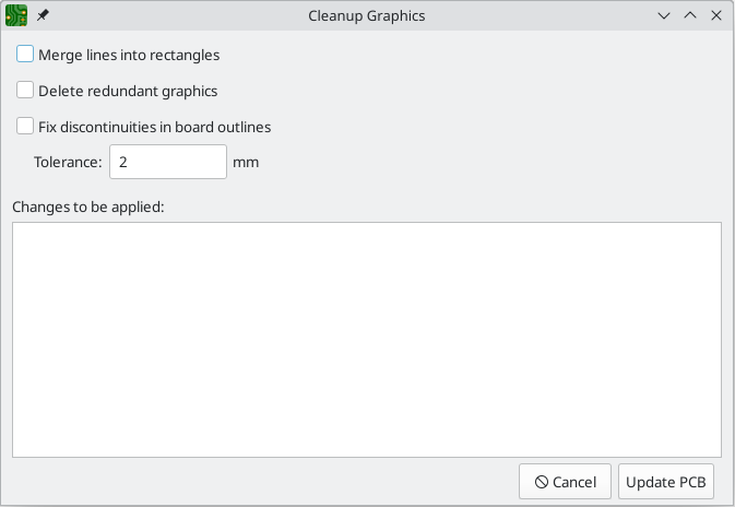
The following cleanup actions are available and will be performed when selected:
-
Merge lines into rectangles: combines individual graphic lines that together form a rectangle into a single rectangle shape object.
-
Delete redundant graphics: deletes graphics objects that are duplicated or degenerate.
-
Fix discontinuities in board outlines: modifies the existing board outline to fix any discontinuities that are within the specified tolerance.
Any changes that will be applied to the board are displayed at the bottom of the dialog. They are not applied until you press the Update PCB button.
Sheet title block
The drawing sheet’s title block is edited with the Page Settings tool (![]() ). You can also open this tool by double clicking on any part of the drawing sheet.
). You can also open this tool by double clicking on any part of the drawing sheet.
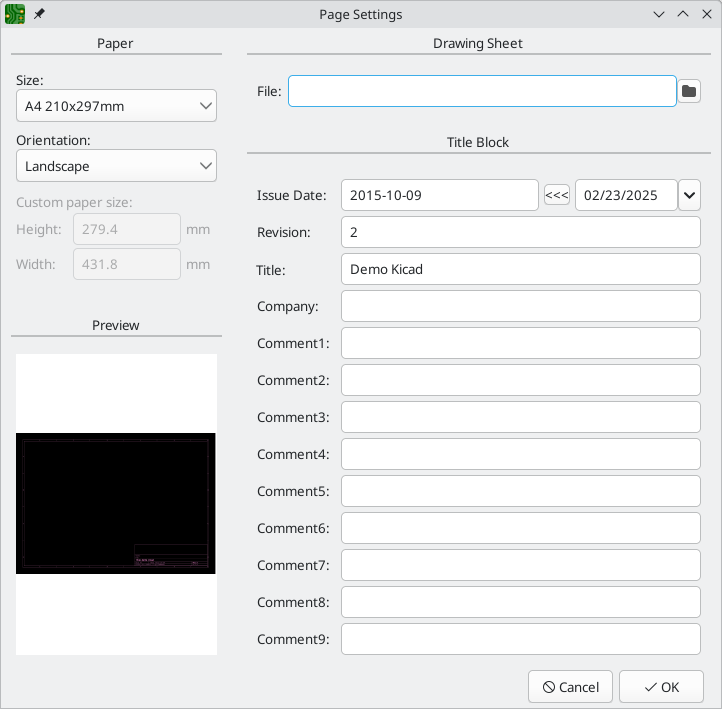
Each field in the title block can be edited, as well as the paper size and orientation.
You can set the date to today’s or any other date by pressing the left arrow button next to Issue Date. Note that the date listed in the board title block is not automatically updated. It is only updated when changed in this dialog.
A drawing sheet file can also be selected to replace the default drawing sheet. When choosing a drawing sheet, you can enable the Embed File checkbox in the file browser to embed the drawing sheet in the board instead of referencing an external file. This means the board will appear the same when it is opened on another computer that does not have the drawing sheet file available at the same external file path. For more information, see the embedded files documentation.
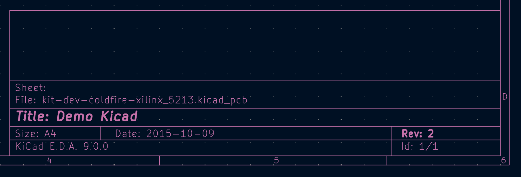
Rule areas (keepouts)
Rule areas, also known as keepouts, are board regions that can have specific DRC rules defined for them. Some basic rules are available that will raise DRC errors if certain types of objects are within the bounds of the rule area, but rule areas can also be used together with custom DRC rules to define complex DRC behavior that only applies within the rule area. Rule areas are also used to define channels for multichannel layout.
You can add a rule area by clicking the ![]() button on the right toolbar (Ctrl+Shift+K). Click on the canvas to place the first corner, which will show the Rule Area Properties dialog. After configuring the rule area appropriately, press OK to continue placing corners of the rule area. The rule area shape can be an arbitrary polygon; click on the starting corner or double click to finish placing the rule area.
button on the right toolbar (Ctrl+Shift+K). Click on the canvas to place the first corner, which will show the Rule Area Properties dialog. After configuring the rule area appropriately, press OK to continue placing corners of the rule area. The rule area shape can be an arbitrary polygon; click on the starting corner or double click to finish placing the rule area.
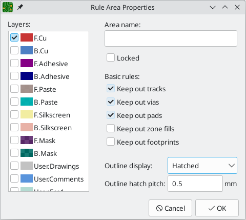
The Rule Area Properties dialog has the following options:
-
The layers list determines which layers the rule area applies to. The area only appears on these layers and the selected keepout rules only apply on these layers. At least one layer must be selected. By default, the active layer in the editing canvas is preselected in the rule area layer list.
-
The area name field is optional and provides an identifier for the rule area. If it is provided, it is included in DRC violation messages to make them clearer. It can also be used in custom DRC rules to identify a particular rule area.
-
The locked checkbox determines if the rule area should be locked. As with other objects, rule areas can also be locked or unlocked after they are created.
-
The Keepouts tab contains several basic rules to prevent various types of objects from being placed within the rule area. The basic rules can be configured to keep out tracks, vias, pads, zone fills, and/or footprints. If an object of one of the selected types is within the rule area, a DRC error will be raised. Additionally, zone fills will automatically avoid a rule area if the rule area is configured to keep out zones.
| Even with no basic rules selected, rule areas can still be used to define specific areas in which to apply custom DRC rules. |
-
The Placement tab contains settings for multichannel layout, which are explained in that section.
-
There are a few options for the outline display of the rule area. The area can be shown with a hatched outline, fully hatched throughout the area, or with just the outline with no hatching. The outline hatch pitch is also adjustable.
锁定
Most objects can be locked through their properties dialogs, by using the right-click context menu, or by using the Toggle Lock hotkey (L). Locking an item makes it more difficult to select, move, or modify the object, which can prevent unintended modifications. Locked objects cannot be selected unless the Locked items checkbox is enabled in the selection filter. Attempting to move locked items will result in a warning dialog:
Selecting Override Locks in this dialog will allow moving the locked items. Selecting OK will allow you to move any unlocked items in the selection; leaving the locked items behind. Selecting Do not show again will remember your choice for the rest of your session.
| You can forget this choice and re-enable the lock override prompt for the current session by unchecking Do not prompt for lock overrides for this session in the Editing Options panel of the PCB Editor Preferences dialog. |
Locked items are displayed with a colored shadow around them. This can be customized in your color scheme.
| Locked objects can’t be selected unless the Locked items checkbox is enabled in the selection filter. By default, this checkbox is disabled to exclude locked items from selection. |
Groups
Groups let you treat multiple objects as a single object for the purposes of moving or rotating them. Each object in the group will maintain its position relative to the other objects in the group. Groups can also have a name, which is displayed in the editing canvas when the group is selected.
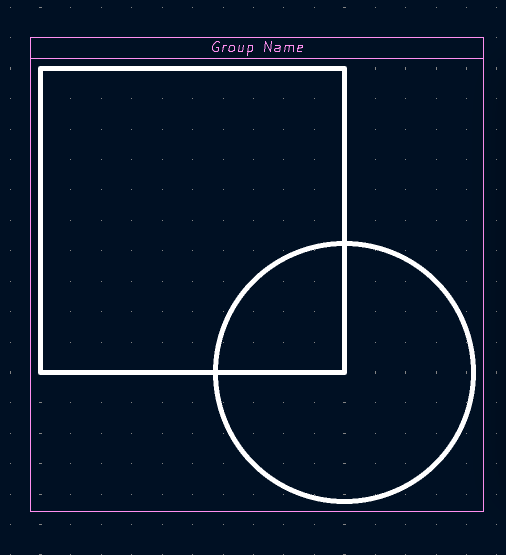
Most types of objects in the Board Editor can be grouped: footprints, tracks, zones, graphic items, and even other groups. Groups can contain multiple different types of objects at once.
To add objects to a group, select them, then right click and choose Grouping → Group Items. To remove all items from a group, select the group, right click, and choose Grouping → Ungroup Items.
Once objects have been added to a group, selecting any of the objects will select the group as a whole instead of the constituent objects. To edit a specific object within a group, first select the group, the right click and choose Enter Group. Double clicking on a group also enters the group. When a group has been entered, objects within the group can be selected and edited individually without affecting the other objects in the group. To leave the group and stop editing its members individually, right click and select Leave Group, select an object outside the group, or use Esc.
There are several ways to modify which objects belong to a group. To remove objects from an existing group, enter the group, then select the objects you want to remove, right click, and choose Grouping → Remove Items. To add items to a group, first ungroup all the items from the group. This will leave the group’s former members selected. Then add the new item to the selection and group the selection. Note that without first ungrouping, this process would create a nested group: a new group containing the new item and the entire original group, not just the items in the original group.
You can also add or remove objects from a group in the group’s properties dialog. To open a group’s properties dialog, press E or right click and click Properties…. The properties dialog lists the objects contained in the group. To add an additional object to the group, click the ![]() button, then click on the desired object in the editing canvas. The object you click on will be added to the group. To remove an object, select it in the list, then click the
button, then click on the desired object in the editing canvas. The object you click on will be added to the group. To remove an object, select it in the list, then click the ![]() button.
button.
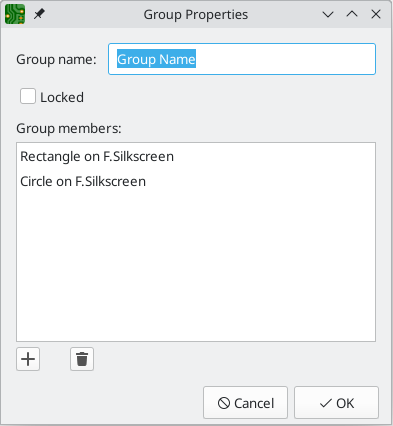
The group properties dialog also lets you specify a name for the group or lock the group. Groups can also be named or locked using the Properties Manager.
Aligning objects
The align tool moves a selection of objects so that they are all aligned with a reference object. There are six different alignments to choose from, depending on which part of the objects you wish to align. Objects can be horizontally aligned by their left, center, or right edges, or they can be vertically aligned by their top, center, or bottom edges. Objects are only moved in one dimension, so objects stay in the same horizontal position when aligned vertically, and vice versa. To align objects by a given edge, select the objects, then right click and choose Align/Distribute → Align to Left (or another alignment as desired).
If the cursor is over an object in the selection, that object is used as the reference object. Otherwise, the reference object is the object in the selection which is located furthest in the alignment direction, for example the leftmost object when aligning by left edge, or the topmost object when aligning by top edge. The topmost object is used when aligning by vertical center, and the leftmost when aligning by horizontal center.
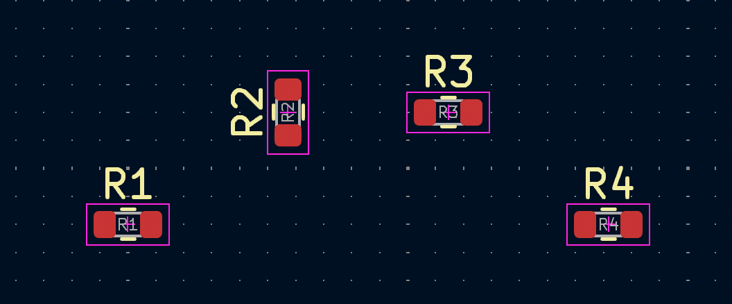
Figure 1. Before alignment
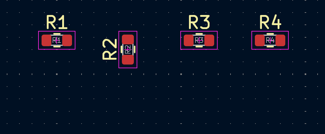
Figure 2. After alignment
In the example above, R1-R4 are vertically aligned by their top edges, with R2 as the reference object. The first image shows them before alignment and the second image shows them after alignment. In this case, R2 is the topmost object before alignment, so it is chosen as the reference object if the cursor is not over another resistor. After alignment, the top edges of the resistors are at the same position, but the horizontal positions of the resistors are unchanged.
Distributing objects
You can use the distribute tool to move objects so they are evenly spaced from each other (right click a selection → Align/Distribute → Distribute Horizontally or Distribute Vertically). The two outermost objects in the selection are not moved. This means the top and bottom objects when distributing vertically, and the leftmost and rightmost objects when distributing horizontally. The remaining objects in the selection are evenly distributed between the outermost objects and maintain their relative ordering. Objects are only moved in one dimension, so objects stay in the same horizontal position when distributed vertically, and vice versa.
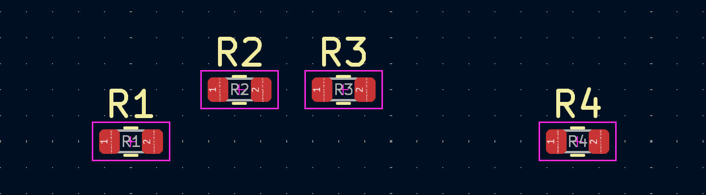
Figure 3. Before distribution
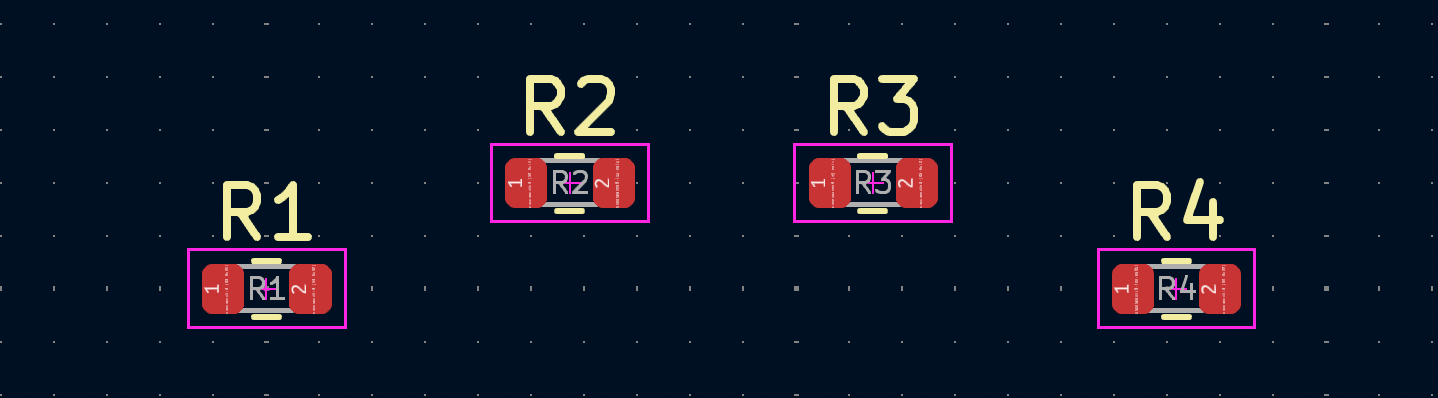
Figure 4. After distribution
In the example above, R1-R4 are horizontally distributed. The first image shows them before distribution and the second image shows them after distribution. R1 and R4 are the leftmost and rightmost objects, so they are not moved. R2 and R3 are moved so the horizontal spacing between resistors is equal, but the vertical positions remain unchanged. From left to right, R1-R4 are in the same order that they were in before distribution.
Arrays
KiCad has an array tool to create rectangular or circular arrays of objects (footprints, vias, graphical objects, etc.). Two types of array are possible: Grid and Circular.
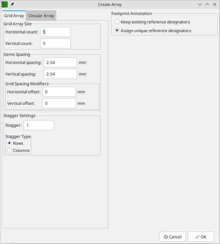
Grid Arrays are rectangular and are described by a horizontal count and a vertical count, which set the number of columns and rows in the array, respectively. The horizontal and vertical spacing settings describe the distance between columns and rows, while the horizontal and vertical offset settings describe a shift applied to each row/column compared to the previous row/column.
You can create a repeating staggered pattern by choosing a stagger setting, which controls the number of rows or columns that are offset before the pattern repeats. You can stagger by row or by column. For example, if two staggered rows are selected, each row will be horizontally offset from the previous row by half of the array’s horizontal spacing setting. Every other row will be placed at the original spacing and offset. If three staggered columns are selected, each column will be vertically offset by a third of the array’s vertical spacing setting. Every third column will be placed at the original spacing and offset. Offsets from the stagger settings are added to the previous horizontal and vertical offset settings.
If the grid position option is set to source items remain in place, the original items will not be moved, and the grid extends with those items at one corner. If center on source items is chosen, the grid is offset so that the resulting grid is centered where the items used to be.
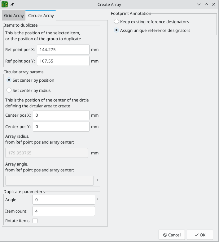
Circular Arrays are described by a center point, an angular spacing, and, optionally, the number of arrayed items. If set center by position is selected, the center point of the array will be defined by the absolute X/Y position you enter in center pos X and center pos Y. You can also interatively select a point from the board using Select Point…, or select the origin point of another item using Select Item….
The item count field determines the number of objects in the array, including the source object. The angle field determines the angular spacing between items, with the center point at the center of the array. Positive angles result in a counter-clockwise rotation relative to the center point and the source item, while negative angles result in a clockwise rotation. Select full circle to evenly space the entered number of items around the circle.
When rotate items is selected, objects will be rotated around their origins as array sweeps around the center point. Otherwise, objects will maintain the same orientation as the source item.
When creating an array of footprints, whether rectangular or circular, the Footprint Annotation settings control how the reference designators will be set in the new footprints. This affects the linkage of the new footprints to the schematic. If keep existing reference designators is selected, the new footprints in the array will have the same reference designators as the source footprints, resulting in duplicated reference designators in the board. If assign unique reference designators is selected, each new footprint created in the array will have a unique reference designator automatically assigned.
| Creating an array of footprints will result in multiple copies of the source footprint(s). If you are using a schematic-based workflow, this will result in footprints that are not represented in the schematic, so careful syncing between the board and the schematic will be needed. |
Multichannel layout
KiCad has a multichannel layout feature for easing designs that have multiple repetitive subcircuits, like an audio mixer with many identical channels. This feature lets you perform placement and routing for one portion of a circuit, then automatically reuse that placement and routing for the other repeated portions of the circuit.
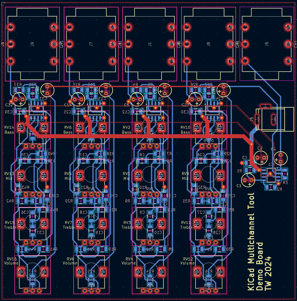
Using the multichannel layout feature first requires you to designate which portions of the schematic represent the repeated parts of the circuit. You can either use hierarchical sheets, with a repeated hierarchical sheet for each channel, or component classes with a unique component class assigned to the symbols in each channel. Each channel will exactly correspond to the symbols (and their associated connections) in a single sheet or component class.
For the layout, specially configured rule areas are drawn on the board and used to describe the physical location of each repeated channel. The automatic placement of footprints, routing, and other items is restricted to these placement rule areas. Each "channel" of the design corresponds to a single rule area. One rule area will be the reference rule area, which will be manually placed and routed. The other rule areas are the target rule areas, which will reuse the placement and routing from the reference rule area.
After setting up the placement rule areas for each channel and manually routing the reference channel, the Repeat Layout tool is used to copy the placement and layout from the reference rule area to the target rule areas.
KiCad includes a demo project, called multichannel, that demonstrates the use of the multichannel layout feature.
|
Multichannel design procedure: schematic
Designing a multichannel layout begins in the schematic. You need to specify which components (symbols) belong to each channel. Each channel in the schematic must be equivalent to the other channels. This means channels must match each other in the following ways:
-
each matched channel needs to have the same number of symbols
-
corresponding symbols in each channel need to have the same reference designator prefix (e.g.
RorU), although the full reference designators need to be unique as usual -
corresponding symbols in each channel need to have the same footprint
-
connections between symbols need to be equivalent in each channel
In the example schematic below, Channels 1, 2, 3, and 4 are equivalent and therefore can be used to share routing in a multichannel design. Even though the net connections are drawn differently in some channels, the underlying net connections are the same. The different symbols in Channel 2 and the different values in Channel 3 also do not break the equivalency. Footprint assignments are not shown in the image, but the symbols that correspond between channels must use the same footprints. In this example, this means that R1, R3, R5, and R7 each must use the same footprint, as must R2, R4, R6, and R8.
In contrast, Channels A and B are not equivalent to Channels 1-4, nor to each other. Channel A contains an extra parallel resistor not present in the other channels, and Channel B is missing a connection between the two resistors.
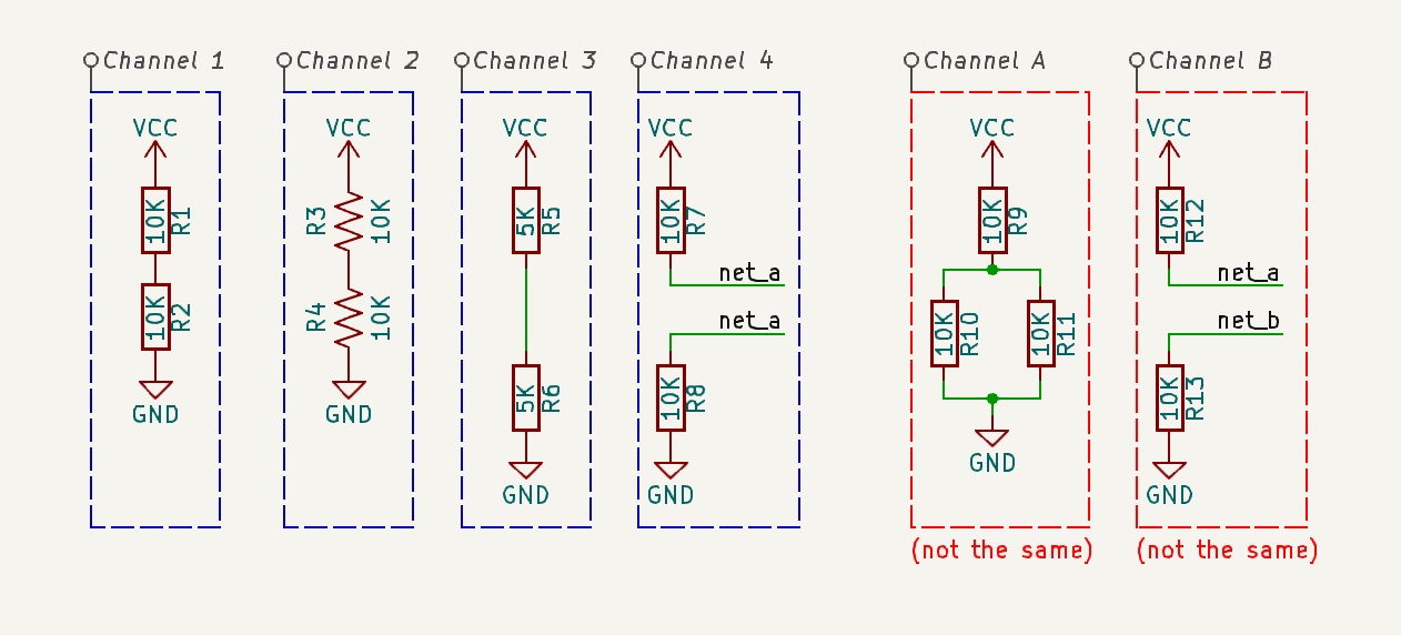
You can assign symbols to channels in two ways, either using hierarchical sheets or using component classes.
-
When doing a multichannel design using hierarchical sheets, each channel is represented by a different sheet. Normally you will instantiate the same hierarchical sheet file multiple times, with one instantiation per channel. Each sheet instantiation needs to include all of the symbols for the corresponding channel, with no extra symbols.
-
When doing a multichannel design using component classes, each channel is represented by a different component class. Each component class needs to include all of the symbols for the corresponding channel, with no extra symbols. Component classes are shown in the previous schematic example.
Multichannel design procedure: board
In the board, each channel is represented with a rule area with its rules configured for placement. You need to add a rule area for each channel. One rule area is the reference, containing manually placed and routed footprints. The other rule areas are targets and have the reference placement and routing copied to them. Placement rule areas, whether for reference or target channels, need the following settings configured in their properties:
-
The options in the Placement tab should be configured to select the hierarchical sheet or component class that contains the channel’s components.
-
The options in the Keepouts tab should typically be unselected, unless there is a specific type of item that needs to be excluded from the rule area.
-
The rule area’s layers should be set based on which layers are considered part of the channel. An item will be copied from the reference channel to a target channel only if the item’s layer is enabled in both the reference and target rule areas.
-
The area name is used to label the rule area when it is listed in the Repeat Layout dialog. While not strictly required, it will be hard for you to distinguish rule areas in the GUI unless each rule area has a unique name.
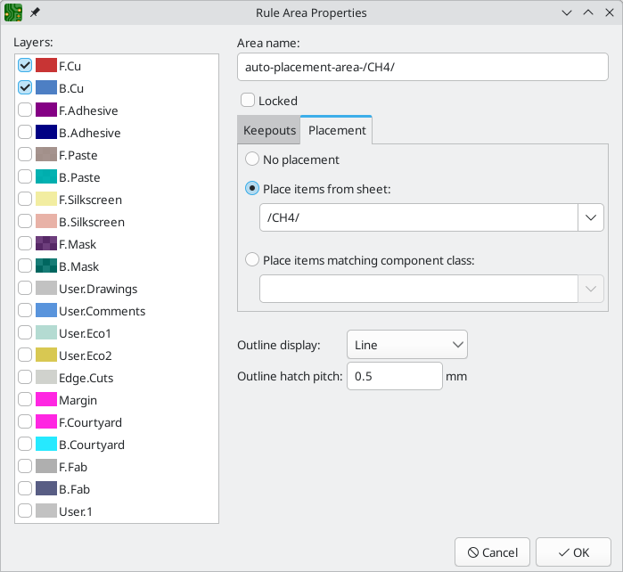
Placement rule areas can be manually created like any rule area, or they can be automatically generated by selecting Tools → Multi-Channel → Generate Placement Rule Areas…. This tool can draw basic placement rule areas for any of the hierarchical sheets or component classes in the design, depending on which you select.
| The tool allows you to generate a placement rule area for any sheet or component class, even if it is not intended to represent a channel in a multichannel design. It is your responsibility to select only the desired sheets or component classes. |
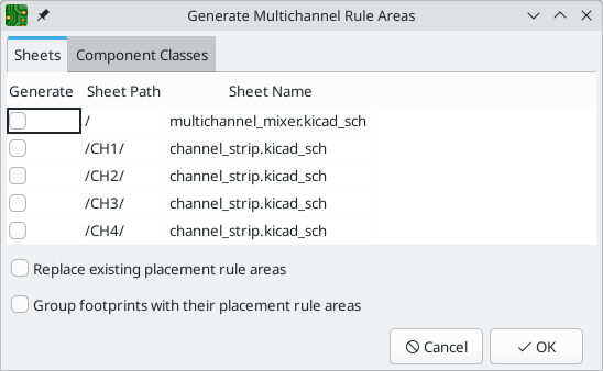
The tool has several options:
-
Replace existing placement rule areas: if enabled, the newly generated rule area for each channel will replace any rule areas that already exist for that channel.
-
Group footprints with their placement rule areas: if enabled, the newly generated rule area for each channel will be added to a group with all footprints associated with that rule area. This allows the target rule area and its associated items to be manipulated as a single entity.
Automatically generated rule areas are preconfigured as placement rule areas with the appropriate source hierarchical sheet or component class selected. Their layers are set to just the front and back copper layers. They are drawn as the minimum size rectangle that encloses their constituent footprints, without extra space for routing or other items. After generating a rule area, you may want to change the configured layers to ensure all desired items in the reference channel get copied to the target channels. You also may want to edit the shape of the rule area, although rule areas for target channels will have their shapes automatically adjusted to match the reference rule area.
| if generated rule areas are grouped with their footprints, you will need to enter the group (or ungroup the items) in order to edit the rule area. |
Once you have created rule areas for each channel and completed placing footprints and routing for the reference channel, you can use the Repeat Layout tool to copy the reference channel’s layout to the other channels. Run this tool using Tools → Multi-Channel → Repeat Layout….
If a rule area is selected when the tool is run, that rule area will be used as the reference rule area. If no rule area is selected, you will be prompted to select a rule area. When the reference rule area is determined, a dialog will appear.
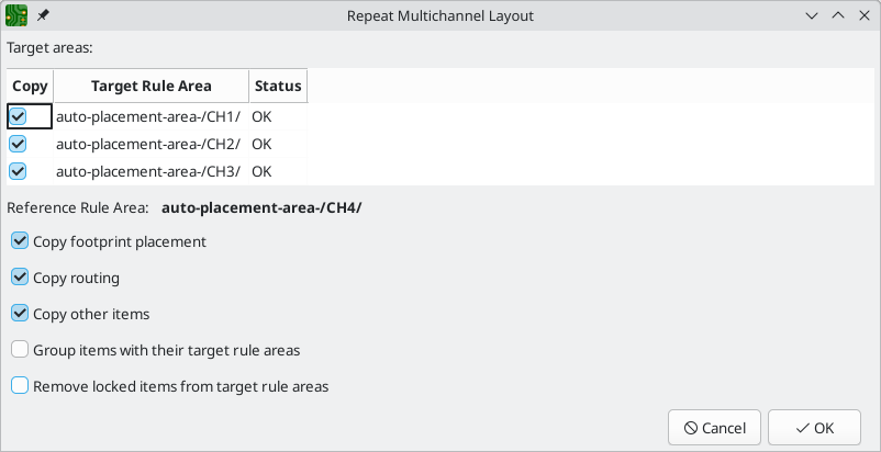
The table at the top of the dialog controls which target rule areas will receive the layout from the reference channel. Any target rule areas that are not selected will not be updated. The tool will only copy items to a target rule area if the target’s status is listed as "OK". If the status is not "OK", the target channel’s circuit topology cannot be matched to the reference channel; see the requirements for how channels need to match in the schematic for more information.
There are several options to control which items from the reference channel are copied to the selected target areas, and how those copied items are handled:
-
Copy footprint placement: if enabled, the placement of footprints in the reference rule area will be replicated for footprints associated with the target rule area(s). Footprints are copied if they are enclosed by or intersect the reference rule area; they are not copied if they are fully outside. Footprints will only be copied if they are on a layer that is enabled in both the reference and target rule areas.
-
Copy routing: if enabled, any tracks and vias in the reference rule area will be copied to the target rule area(s). Routing is copied if it is enclosed by or intersects the reference rule area; it is not copied if it is fully outside. Routing will only be copied if it is on a layer that is enabled in both the reference and target rule areas.
-
Copy other items: if enabled, any other items (zones, graphic objects) fully enclosed by the reference rule area will be copied to the target rule area(s). Items are copied if they are fully enclosed by the reference rule area; they are not copied if they are partially or fully outside. This means, for example, that a large copper zone that intersects a reference channel will not be copied to the target channels. Items will only be replicated if they are on a layer that is enabled in both the reference and target rule areas.
-
Group items with their placement rule areas: if enabled, the items copied to a target rule area will be added to a group with that rule area. This allows the target rule area and its associated items to be manipulated as a single entity.
-
Remove locked items from target rule areas: if enabled, items associated with target rule areas will be updated even if they are locked. If not enabled, locked items will not be updated to match the reference rule area.
After clicking OK, the layout from the reference channel will be applied to the target channels. When the repeat layout is completed, each channel can be individually edited like any other part of the board design.
Using reference images
KiCad supports displaying reference images in the canvas. These are background images that you can use to help you lay out a board; they are purely for reference during the design process and are not included in any fabrication outputs.
To add a reference image, use the ![]() button on the right toolbar and select the desired reference image file. Click in the canvas to place the image.
button on the right toolbar and select the desired reference image file. Click in the canvas to place the image.
Once the image has been added to the canvas, you can reposition it using the move tool (M) or by dragging it in the canvas. You can scale it by dragging the editing handles at the corners of the image. The image is scaled around its reference point; in other words, the reference point is the point in the image that always stays in the same position in the canvas, no matter how the image is scaled. The reference point is shown as a fifth editing handle. Initially it is at the center of the image, but you can reposition the reference point by dragging it in the canvas.
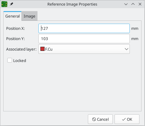
You can also reposition or scale the image in its properties dialog (E). You can set the image’s exact Position X and Y in the General tab, and set an exact Scale factor in the Image tab. You can also Convert to Greyscale if you wish. Position and scale in this dialog are relative to the center of the image, not its interactive reference point.
Reference images have an associated board layer; they are shown and hidden along with this layer. The layer initially associated with a reference image is the layer that was active when the image was added. You can change the associated layer in the image’s properties.
Another way to hide reference images is with the Appearance Manager. You can show or hide all reference images by toggling the visibility of Image objects in the Objects tab (![]() button). You can also adjust the opacity of reference images here.
button). You can also adjust the opacity of reference images here.