创建 PCB
PCB 的基本概念
KiCad 中的印刷电路板通常由代表电子元件及其焊盘的 封装、定义这些焊盘如何彼此连接的 网络、形成每个网络中焊盘之间的铜连接的 布线、过孔 和 敷铜 以及定义电路板边缘、丝印标记和任何其他所需信息的各种图形形状组成。
KiCad 通常会将 PCB 上的网络信息与相关的原理图保持同步,但也可以直接在 PCB 编辑器中创建和编辑网络。
性能
KiCad 能够创建多达 32 个铜层、14 个技术层 (丝印、阻焊、元件粘合剂、锡膏等) 和 13 个通用绘图层的印刷电路板。
KiCad 中所有对象的内部测量分辨率为 1 纳米,测量值以 32 位整数存储。 这意味着可以创建最大约 4 米乘 4 米的电路板。
KiCad 目前支持每个工程/原理图一个电路板文件。
从原理图开始
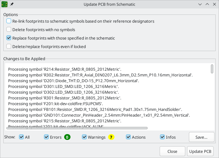
Creating a board from a schematic is the recommended workflow for KiCad. When you create a new project, KiCad will generate an empty board file with the same name as the project. To start designing the board after you have created a schematic, simply open the board file. You can do this either from the KiCad project manager, or by clicking the "Open PCB in board editor" button in the schematic editor. To import the schematic design information into the board editor, including footprints and net connections, use the Tools → Update PCB from Schematic… action (F8). You can also use the ![]() icon in the top toolbar.
icon in the top toolbar.
| 从原理图更新 PCB 是将设计信息从原理图转移到 PCB 的首选方法。在旧版本的 KiCad 中,相应的过程是将网表从原理图编辑器中导出并导入到电路板编辑器中。现在已经没有必要使用网表文件了。 |

关于从原理图更新PCB工具的更多信息,请参见手册的 [正向批注,正向批注] 部分。
从头开始
也可以创建一个没有匹配原理图的电路板,不过这种工作流程有一些限制,不建议大多数用户使用。为此,您必须独立启动 PCB 编辑器(而不是从 KiCad 工程管理器启动)。在开始设计之前,最好先保存电路板文件,这也将创建一个项目文件来存储电路板设置。 使用文件菜单中的 "另存为… " 来选择保存电路板文件的位置。一个具有相同名称的项目文件将被创建在你选择保存电路板文件的相同位置。
电路板设置
在开始设计电路板之前,使用电路板设置对话框来配置电路板的基本参数。要打开电路板设置,请单击顶部工具栏中的 ![]() 图标或从文件菜单中选择 "电路板设置…"。
图标或从文件菜单中选择 "电路板设置…"。
配置电路板层叠和物理参数
在 "电路板设置" 中,有两个部分用于配置电路板的层叠和层。 "电路板编辑器层" 部分用于启用或禁用技术层(非铜层),如果需要的话,还可以给各层自定义名称。 物理层叠部分用于配置铜层的数量,以及铜层和电介质层的物理参数,如厚度和材料类型。介电层、阻焊层和丝印层可以被分配颜色,这将影响电路板在 3D 查看器中的外观。
要配置电路板的层叠,从物理层叠部分开始:
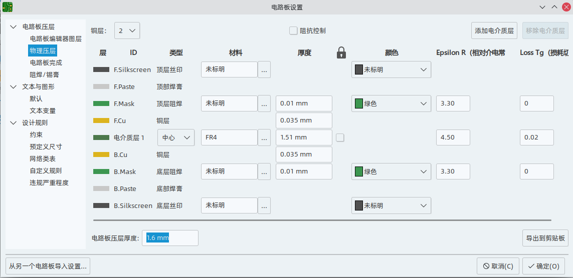
Set the number of copper layers in the upper left corner and then enter the physical parameters of the stackup if desired. These parameters may be left at their default values, but note that the board thickness value will be used when exporting a 3D model of the board, and layer thicknesses will be included in net length calculations for any nets that include vias. If you plan to use these features, it is a good idea to ensure that the stackup thickness is correct.
| KiCad 目前仅支持铜层数为偶数的层叠。 要创建具有奇数层的设计 (例如,柔性印刷电路板或金属芯印刷电路板), 只需选择下一个最高的偶数,而忽略多余的层。 |
Next, if desired, use the Board Editor Layers section to rename layers or hide non-copper layers that you will not be using in the design. For example, if you will not use a back silkscreen on the design, uncheck the box next to the B.Silkscreen layer. Some layers, like F.Cu / B.Cu or Edge.Cuts, are required layers and therefore cannot be disabled.
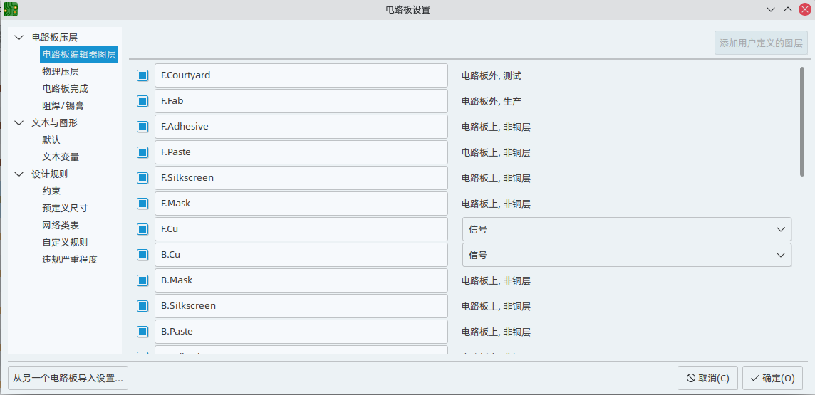
| 在电路板编辑器层部分,可以将铜层指定为信号层、电源层、混合层或跳线层。 本指南仅供用户参考。 无论在此对话框中将类型配置为什么,都可以在任何铜层上布线和敷铜。 |
You can add additional user-defined layers (User.1, User.2, etc.) by clicking the Add User Defined Layer… button in the top right. User-defined layers can’t be used for routing, but they can contain arbitrary graphics or other information. By default, user layers are auxiliary layers, meaning that whatever information they contain does not correspond to either the front or back of the board. User layers can instead be set to Off-board, front or Off-board, back, in which case they correspond to the selected side of the board. Items on such layers can be flipped from front to back in the same way as objects on physical front/back layers. Adjacent front/back layers are treated as paired: if User.2 is defined as a front layer and User.3 is defined as a back layer, flipping an object on User.2 will move it to User.3, and vice versa.
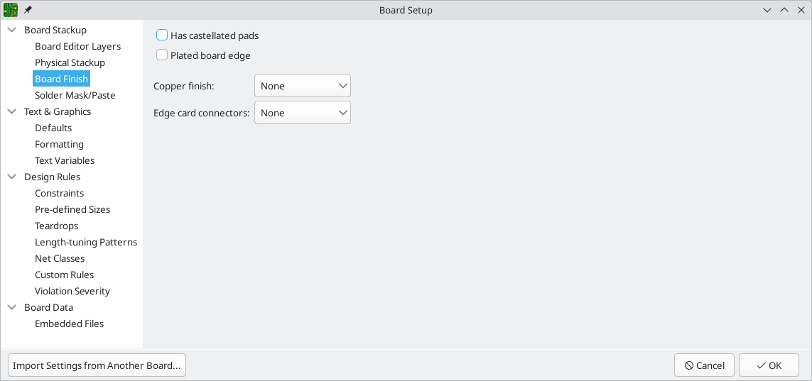
在电路板编辑器对话框的电路板表面处理(Board Finish)和阻焊/锡膏部分可以找到一些其他的电路板层叠设置。电路板表面处理部分包含用于定义铜的表面处理和特殊功能 (如刻痕或边缘电镀) 的设置。请注意,这些设置目前只影响作为 Gerber 文件一部分的电路板属性输出。
阻焊/锡膏部分允许全局调整电路板上焊盘的铜形和阻焊/锡膏形之间的间隙(正或负)。 这些值将被添加到在个别封装或焊盘上设置的任何间隙覆盖。 正的间隙值将导致阻焊层或锡膏开口的形状比铜的形状 更大。 负的间隙值将导致开口比铜的形状 更小。
| 大多数商业 PCB 制造商希望这些值为零,并在 CAM 过程中自行调整阻焊和锡膏开口。 通常最好将这些值保留为默认值零, 除非您自己制作 PCB, 或者您的制造商有具体建议使用不同的值。 |
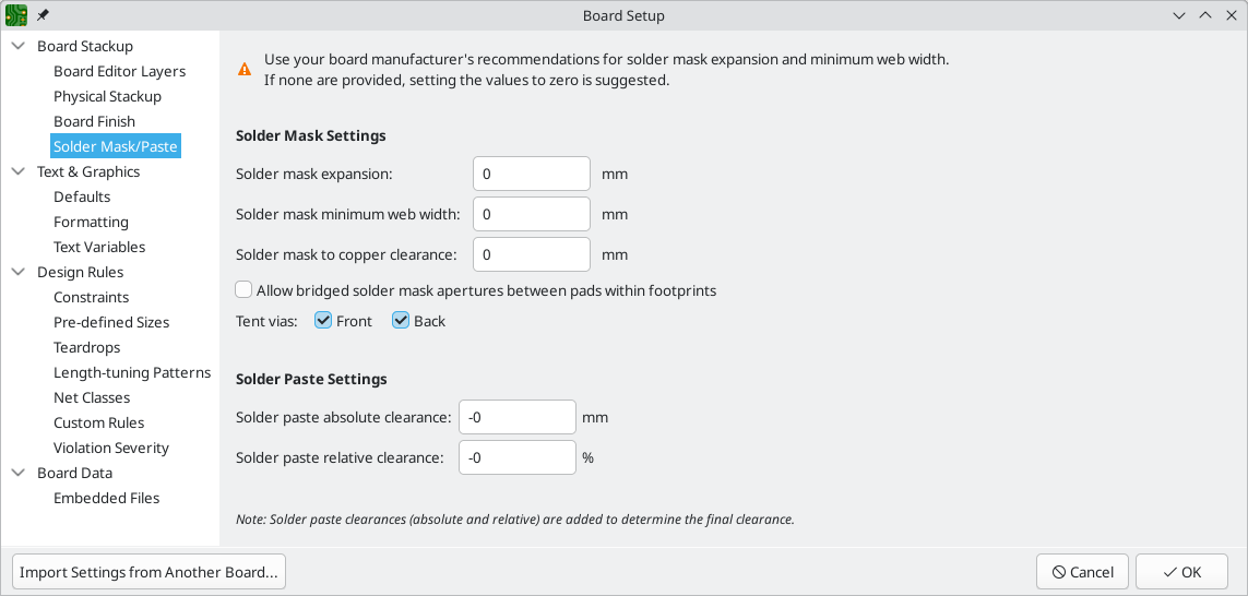
配置默认文本和图形设置
电路板设置对话框的文本和图形默认值部分可用于配置将用于放置在电路板上的新文本和图形形状的属性。
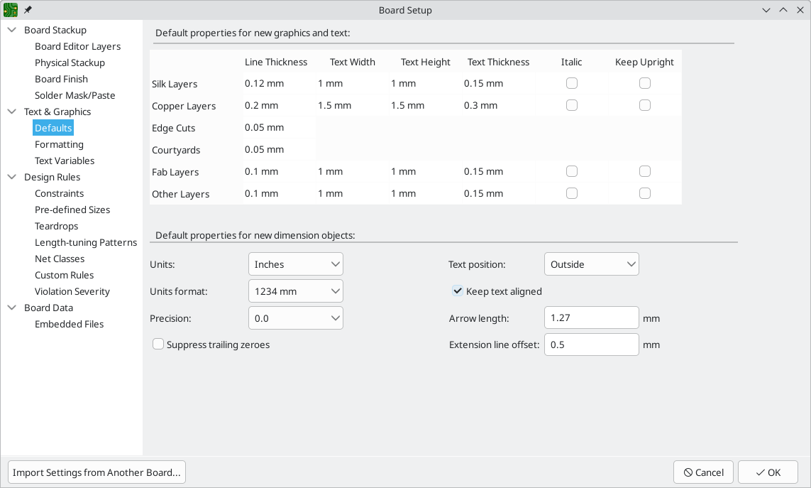
可以为对话框中显示的六种不同类别的图层配置线粗细、文本大小和文本外观。此外,可以为所有图层配置标注对象的特性。有关标注属性的更多详细信息,请参阅下面的标注部分。
虚线的外观是在 "格式化" 部分控制的。虚线长度 控制虚线的长度,而 间隔长度 控制虚线和圆点之间的间距。虚线和间隔的长度是相对于行宽而言的:间隔长度为 2 意味着是行宽的两倍。
文本替换变量可以在文本变量部分创建。 这些变量允许你将变量名称替换为任何文本字符串。 这种替换发生在变量名称在 ${VARIABLENAME} 的变量替换语法内的任何地方。
例如,您可以创建一个名为 VERSION 的变量,并将文本替换设置为 1.0。 现在,在 PCB 上的任何文本对象中,你可以输入 ${VERSION},KiCad 将替代 1.0。 如果你把变量改为 2.0,每个包括 ${VERSION} 的文本对象都会自动更新。 你也可以混合使用普通文本和变量。 例如,你可以创建一个文本对象,内容为 版本:${VERSION},它将被替换为 版本:1.0。
文本变量也可以在 原理图设置 中创建。 文本变量是项目范围内的;在原理图编辑器中创建的变量在电路板编辑器中也可用,反之亦然。
还有一些 内置系统文本变量。
配置设计规则
Design rules control the behavior of the interactive router, the filling of copper zones, and the design rule checker. Design rules can be modified at any time, but we recommend that you establish all known design rules at the beginning of the board design process.
约束
Basic design rules are configured in the Constraints section of the Board Setup dialog. Constraints in this section apply to the entire board and should be set to the values recommended by your board manufacturer. Any minimum value set here is an absolute minimum and cannot be overridden with a more specific design rule. For example, if you need the copper clearance on part of a board to be 0.2mm and in the rest 0.3mm, you must enter 0.2mm for the minimum copper clearance in the Constraints section and use a net class or custom rule to set the larger 0.3mm clearance.
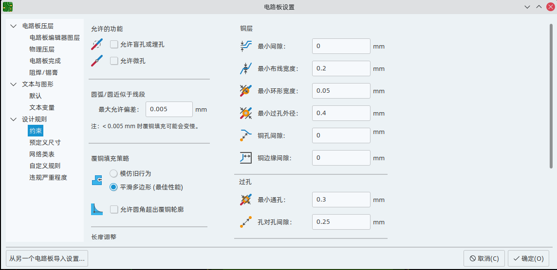
除了设置最小间隙外,还可以在此处配置许多功能:
| Setting | Description |
|---|---|
Arc/circle approximated by segments |
In some situations, KiCad must use a series of straight line segments to approximate round shapes such as those of arcs and circles. This setting controls the maximum error allowed by this approximation: in other words, the maximum distance between a point on one of these line segments and the true shape of the arc or circle. Setting this to a lower number than the default value of 0.005mm will result in smoother shapes, but can be very slow on larger boards. The default value typically results in arc approximation error that is not detectable in the manufactured board due to manufacturing tolerances. |
Allow fillets outside zone outline |
Zones can have fillets (rounded corners) added in the Zone Properties dialog. By default, no zone copper, including fillets, is allowed outside the zone outline. This effectively means that inside corners of the zone outline will not be filleted even when a fillet is configured. By enabling this setting, inside corners of the zone outline will be filleted even though this results in copper from the zone extending outside the zone outline. |
Minimum thermal relief spoke count |
This sets the minimum acceptable number of thermal relief spokes connecting a pad to a zone. A DRC violation will be generated if this constraint is violated. |
Include stackup height in track length calculations |
By default, the length tuner uses the height of the stackup to calculate the additional length of a track that travels through vias from one layer to another. This calculation relies on the board stackup height being correctly configured. In some situations, it is preferable to ignore the height of vias and just calculate the track length assuming that vias add no length. Disabling this setting will exclude via length from length tuner track length calculations. |
预定义大小
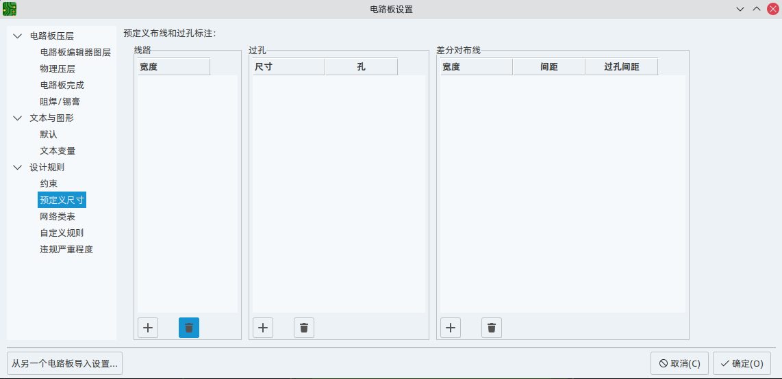
The pre-defined sizes section allows you to define the track and via dimensions you want to have available while routing tracks. Net classes can be used to define the default dimensions for tracks and vias in different nets (see below) but defining a list of sizes in this section will allow you to step through these sizes while routing. For example, you may want the default track width on a board to be 0.2 mm, but use 0.3 mm for some sections that carry more current, and 0.15 mm for some sections where space is limited. You can define each of these track widths in the Board Setup dialog and then switch between them when routing tracks.
Teardrops
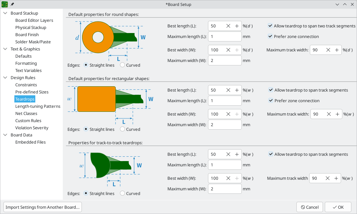
The teardrops section lets you set default parameters for various types of teardrops. There are different settings for teardrop connections to round objects, rectangular objects, and teardrop connections between tracks. The default teardrop parameters can be overridden when teardrops are added, and also changed in the properties for individual connected items. See the teardrops documentation for more information about each setting.
Length-tuning patterns
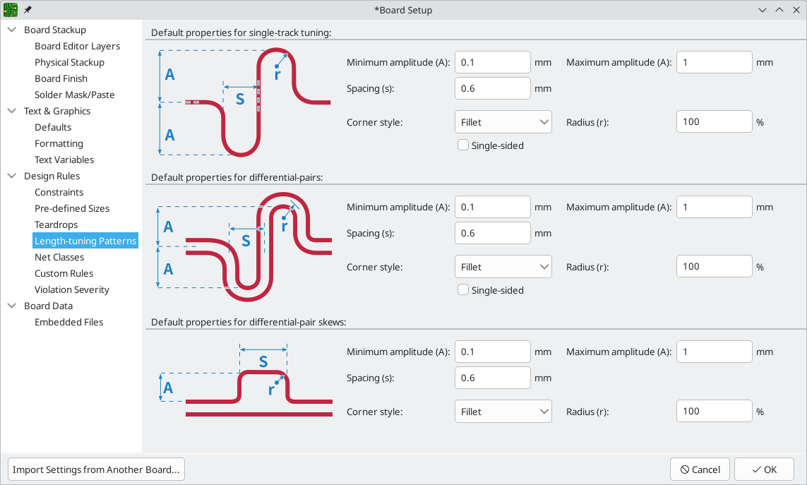
The length-tuning patterns section lets you set default parameters for each type of length-tuning pattern (single-track length, differential-pair length, and differential-pair skew). These defaults can be overridden in the properties of each tuning pattern added to the board. See the length tuning documentation for more information.
网络类
The Net Classes section allows you to configure routing and clearance rules for different classes of nets.
More than one net class can be assigned to a net. For nets with multiple net classes assigned, an effective aggregate net class is formed, taking any net class properties from the highest priority net class which has that property set. Net class priority is determined by the ordering in the Schematic or Board Setup dialogs. The Default net class is used as a fallback for any missing properties after all explicit net classes have been considered; this means that nets may be part of the Default net class even if they have other net classes explicitly assigned.
Net classes may be created and edited in either the Schematic or Board Setup dialogs.
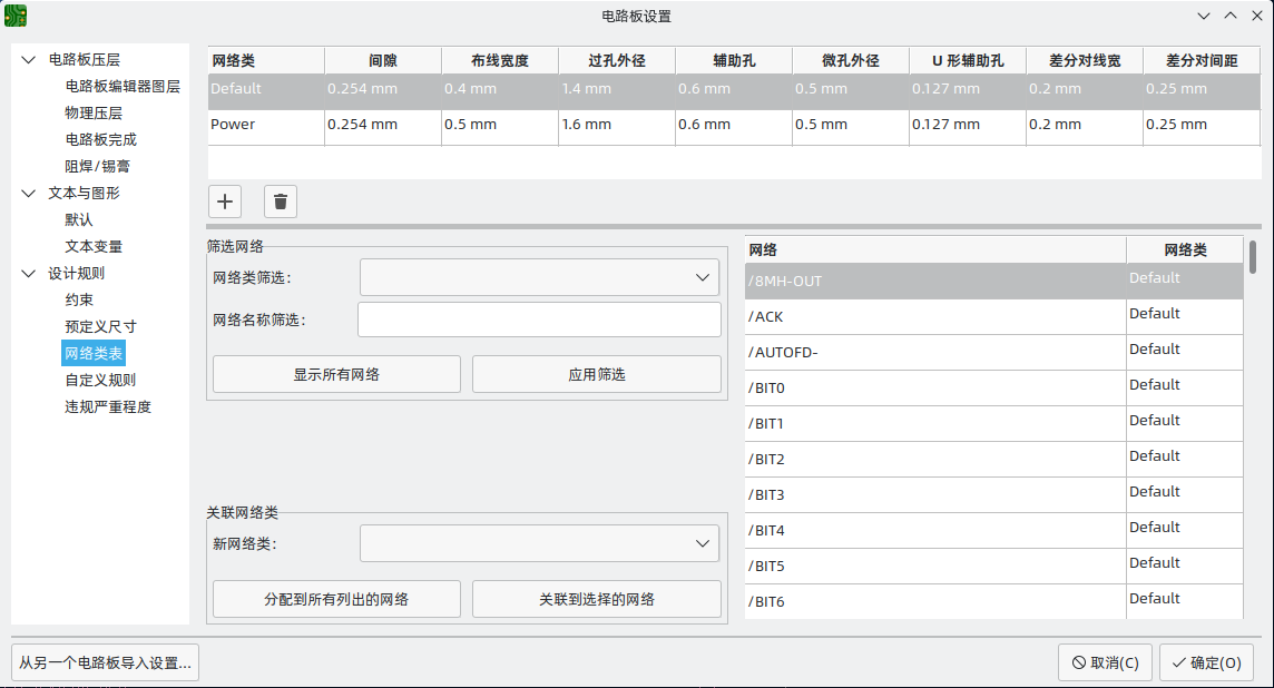
网络类部分的上部有一个表格,显示了设计中的网络类和适用于每个网络类的设计规则。 每个类别都有铜的间隙、布线宽度、过孔尺寸和差分对尺寸的值。 这些值将在创建布线和过孔时使用,除非有更具体的规则覆盖它们(见下面的自定义规则)。
任何规则都不能覆盖电路板设置的约束条件部分中设置的最小值。
例如,如果您将网络类间距设置为 0.1 mm,但约束条件部分中的最小间距设置为 0.2 mm,
则该类网络的间距将为 0.2 mm。
|
The track widths and via sizes defined for each net class are used when the track width and via size controls are set to "use netclass values" in the PCB editor. These widths and sizes are considered the default, or optimal, sizes for that net class. They are not minimum or maximum values. Manually changing the track width or via size to a different value from that defined in the Net Classes section will not result in a DRC violation. To restrict track width or via size to specific values, use Custom Rules.
Each net class can also have a color assigned to it. Depending on how net colors are configured in the appearance panel, net class colors can override the default color for ratsnest lines or copper objects. In addition to arbitrary colors for each net class, you can set all net classes to use the same color as configured for them in the schematic editor by clicking the Import colors from schematic button. To use a layer’s default color instead of overriding it with a custom net class color, set the net class color to transparent.
The lower portion of the Net Classes section lists pattern-based net class assignments. Working with pattern-based net class assignments is explained in the Schematic Editor documentation; pattern-based assignments can be edited in either the Board or Schematic Setup windows.
Note that pattern-based assignments can be created directly from the PCB editing canvas by right clicking a copper track or zone and clicking Assign netclass…. Net classes can also be assigned in the schematic using net class directives or labels instead of pattern-based assignments.
自定义规则
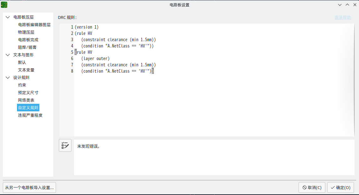
自定义规则部分包含一个文本编辑器,用于使用自定义规则语言创建设计规则。 自定义规则用于创建基本约束或网络类设置没有涵盖的特定设计规则检查。
只有在自定义规则定义中没有错误时,才会应用自定义规则。 在关闭电路板设置之前,使用检查规则语法器按钮来测试定义并修复任何问题。
See Custom Design Rules in the Advanced Topics chapter for more information on the custom rules language as well as example rules.
违规严重程度
违规严重性部分允许你配置每种设计规则检查的严重性。 每条规则可以被设置为创建一个错误标记、一个警告标记或没有标记(忽略)。
| 在设计规则检查器中可能会忽略个别规则违规。 在违规程度部分中将规则设置为忽略将完全禁用相应的设计规则检查。 请谨慎使用此设置。 |
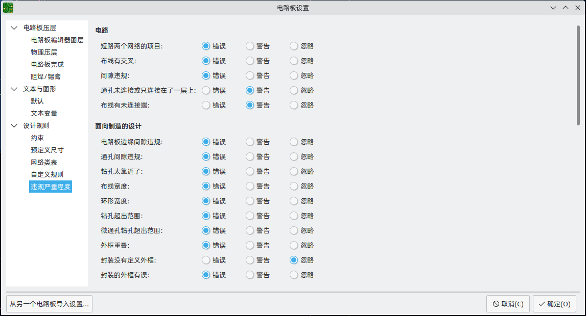
For descriptions of each violation type, and how to ignore individual violations without disabling all violations of that type, see the DRC documentation.
Embedding files
External files can be embedded within a board file. Embedding a file stores a copy of the file inside the board file. The design can then refer to the embedded copy of the file instead of the external file, which makes the project more portable as it doesn’t rely on an external file. Fonts, datasheets, drawing sheets, SPICE models, and footprint 3D models can be embedded and used within KiCad. Other arbitrary files can also be embedded to store them in the project for later export, but they are not used by any KiCad functionality. Files embedded in a board necessarily increase the board’s file size, although files are compressed before being embedded to minimize the space required.
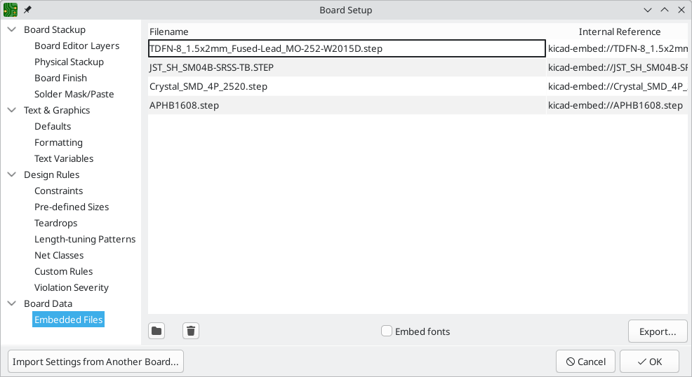
Embedded files are managed in the Embedded Files section of Board Setup. All files embedded in a board are shown here. To embed a file inside a board, click the ![]() button and select the file. The file is then embedded inside the PCB and is listed in the embedded files list along with its embedded reference. The embedded reference is a unique identifier for the embedded file that begins with
button and select the file. The file is then embedded inside the PCB and is listed in the embedded files list along with its embedded reference. The embedded reference is a unique identifier for the embedded file that begins with kicad-embed://. You can use the embedded reference elsewhere in the Board Editor to refer to the embedded file as if it were an external file path. You can copy the embedded reference by right clicking and selecting Copy Embedded Reference. To remove an embedded file, click the ![]() button. Any remaining links to the removed file will become invalid.
button. Any remaining links to the removed file will become invalid.
| 3D models and drawing sheets can be embedded directly using the file browser when you add them to a footprint (3D models) or to a board (drawing sheets) by enabling the Embed Files option in the file browser. This is a single-step shortcut for adding the files in Board Setup and then referring to them by their embedded reference; the result is the same. |
To embed any fonts used in a board, check the Embed fonts checkbox. All fonts used in the board design will be embedded, so text using that font can be edited on any computer regardless of whether the font file is installed.
You can also embed files in a footprint, either in the board copy of a footprint or in a library. Such files will be available within the footprint instance but not within the larger board design or within other footprints. Files embedded in a footprint are deduplicated when the footprint is added to a board: if a file is embedded in a footprint, and multiple instances of that footprint are added to the board, only one copy of the file will be embedded, and all of the footprint instances will refer to the same embedded file.
As an example, to embed a 3D model in a project and use it within several footprints, you could embed the model using the Board Setup dialog, copy the internal reference, and paste the internal reference as a 3D model path in each footprint that uses that model. Alternatively, you could embed the model within a single footprint, either in the board or in the source footprint library. In this case, the footprint itself is portable if you export the footprints from the board, and the model embedding is managed in the footprint’s properties rather than Board Setup. A more convenient way to achieve the same thing, however, is to open the footprint’s properties dialog, add a 3D model file, and enable the Embed File option in the file browser. Again, this could be done for a footprint in the board or for a footprint in the source footprint library.
Files can also be embedded in schematics.
导入设置
您可以从现有电路板导入部分或全部电路板设置。 这种技术可以用来创建一个 "模板" 电路板板,其中有你想在多个设计中使用的设置,然后将这些设置从模板板中导入到每个新板中,而不是手动输入。
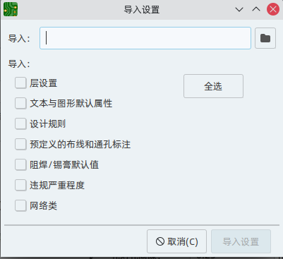
To import settings, click the Import Settings from Another Board… button at the bottom of the Board Setup dialog and then choose the kicad_pcb file you want to import from. Select which settings you want to import and the current settings will be overwritten with the values from the chosen board.
The settings that are available to import are:
-
Board layers and physical stackup
-
Solder mask/paste defaults
-
Text and graphics default properties
-
Text & graphics formatting
-
Design rule constraints
-
Predefined track & via dimensions
-
Teardrop defaults
-
Length-tuning pattern defaults
-
Net classes
-
Custom rules
-
Violation severities