高级主题
配置和自定义
KiCad PCB 编辑器有多种偏好设置,可通过偏好设置对话框进行配置。和 KiCad 的所有部分一样,PCB 编辑器的偏好设置存储在用户配置目录中,并且在 KiCad 的小版本之间是独立的,以允许多个版本的偏好设置分别运行。
偏好设置对话框的第一部分(通用、鼠标和触摸板以及快捷键)是所有 KiCad 程序共享的。这些部分在 KiCad 手册中的 "常规偏好设置" 部分有详细描述。
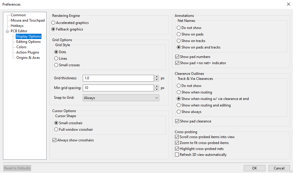
显示选项
Rendering Engine: Controls if Accelerated graphics or Fallback graphics are used.
Grid style: Controls how the alignment grid is drawn.
Grid thickness: Controls how thick grid lines or dots are drawn.
Min grid spacing: Controls the minimum distance, in pixels, between two grid lines. Grid lines that violate this minimum spacing will not be drawn, regardless of the current grid setting.
Snap to grid: Controls when drawing and editing operations will be snapped to coordinates on the active grid. "Always" will enable snapping even when the grid is hidden; "When grid shown" will enable snapping only when the grid is visible.
| 按住 Ctrl 可以暂时禁用网格捕捉。 |
Cursor shape: Controls whether the editing cursor is drawn as a small crosshair or a full-screen crosshair (a set of lines covering the entire drawing canvas). The editing cursor shows where the next drawing or editing action will occur and will be snapped to a grid location if snapping is enabled.
Always show crosshairs: Controls whether the editing cursor is shown all the time or only when an editing or drawing tool is active.
Net names: Controls whether or not net name labels are drawn on copper objects. These labels are guides for editing only and do not appear in fabrication outputs.
Show pad numbers: Controls whether or not pad number labels are drawn on footprint pads.
Show pad <no net> indicator: Controls whether or not pads with no net are indicated with a special marker.
Track clearance: Controls whether or not clearance outlines around tracks and vias are shown. Clearance outlines are shown as thin shapes around objects that indicate the minimum clearance to other objects, as defined by constraints and design rules.
Show pad clearance: Controls whether or not clearance outlines around pads are shown.
Center view on cross-probed items: When the Schematic and PCB Editors are both running, controls whether clicking a component or pin in Eeschema will center the PCB Editor view on the corresponding footprint or pad.
Zoom to fit cross-probed items: Controls whether the view will be zoomed to show a cross-probed footprint or pad.
Highlight cross-probed nets: Controls whether or not nets highlighted in Eeschema will be highlighted in the PCB Editor when the highlight tool is activated in both tools.
编辑选项
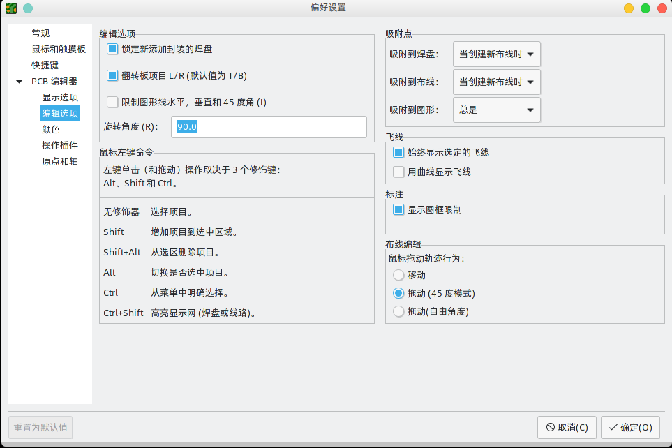
Flip board items L/R: Controls the direction board items will be flipped when moving them between the top and bottom layers. When checked, items are flipped Left-to-Right (about the Vertical axis); when unchecked, items are flipped Top-to-Bottom (about the Horizontal axis).
Step for rotate commands: Controls how far the selected object(s) will be rotated each time the Rotate command is used.
Allow free pads: Controls whether or not the pads of footprints can be unlocked and edited or moved separately from the footprint.
Magnetic points: This section controls object snapping, also called magnetic points. Object snapping takes precedence over grid snapping when it is enabled. Object snapping only works to objects on the active layer. Hold Shift to temporarily disable object snapping.
Snap to pads: Controls when the editing cursor will snap to pad origins.
Snap to tracks: Controls when the editing cursor will snap to track segment endpoints.
Snap to graphics: Controls when the editing cursor will snap to graphic shape points.
Always show selected ratsnest: When enabled, the ratsnest for a selected footprint will always be shown even if the global ratsnest is hidden.
Show ratsnest with curved lines: Controls whether ratsnest lines are drawn straight or curved.
Mouse drag track behavior: Controls the action that will occur when you drag a track segment with the mouse: "Move" will move the track segment independent of any others. "Drag (45 degree mode)" will invoke the push-and-shove router to drag the track, respecting design rules and keeping other track segments attached. "Drag (free angle)" will move the nearest corner of the track segment, highlighting collisions with other objects but not moving them out of the way.
Limit actions to 45 degrees from start Controls whether lines drawn with the graphic drawing tools can take on any angle. Note that this only affects drawing new lines: lines can be edited to take on any angle.
Show page limits: Controls whether or not the page boundary is drawn as a rectangle.
Refill zones after Zone Properties dialog: Controls whether or not zones are automatically refilled after editing the properties of any zone. This may be disabled on complicated designs or slower computers to improve responsiveness.
颜色
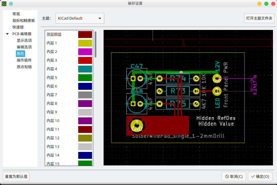
KiCad supports switching between different color themes to match your preferences. Kicad 9.0 comes with two built-in color themes: "KiCad Default" is a new theme designed to have good contrast and balance for most cases and is the default for new installations. "KiCad Classic" is the default theme from KiCad 5.1 and earlier versions. Neither of these built-in themes can be modified, but you can create new themes to customize the look of KiCad as well as install themes made by other users.
颜色主题存储在位于 KiCad 配置目录的 Colors 子目录中的 JSON 文件中。“打开主题文件夹” 按钮将在您的系统文件管理器中打开此位置,使您可以轻松地管理已安装的主题。要安装新主题,请将其放在此文件夹中,然后重新启动 KiCad。如果文件是有效的颜色主题文件,则从颜色主题下拉列表中可以看到新主题。
要创建一个新的颜色主题,从颜色主题的下拉列表中选择 “新主题…”。 为你的主题输入一个名称,然后开始编辑颜色。 新主题中的颜色将从你创建新主题之前选择的任何主题中复制。
要更改颜色,请双击或中键单击列表中的色样。“重置为默认值” 按钮会将该颜色重置为 “KiCad 默认” 颜色主题中的相应条目。
颜色主题会自动保存;当您关闭 "偏好设置" 对话框时,所有更改都会立即反映出来。对话框右侧的窗口显示所选主题外观的预览。
操作插件
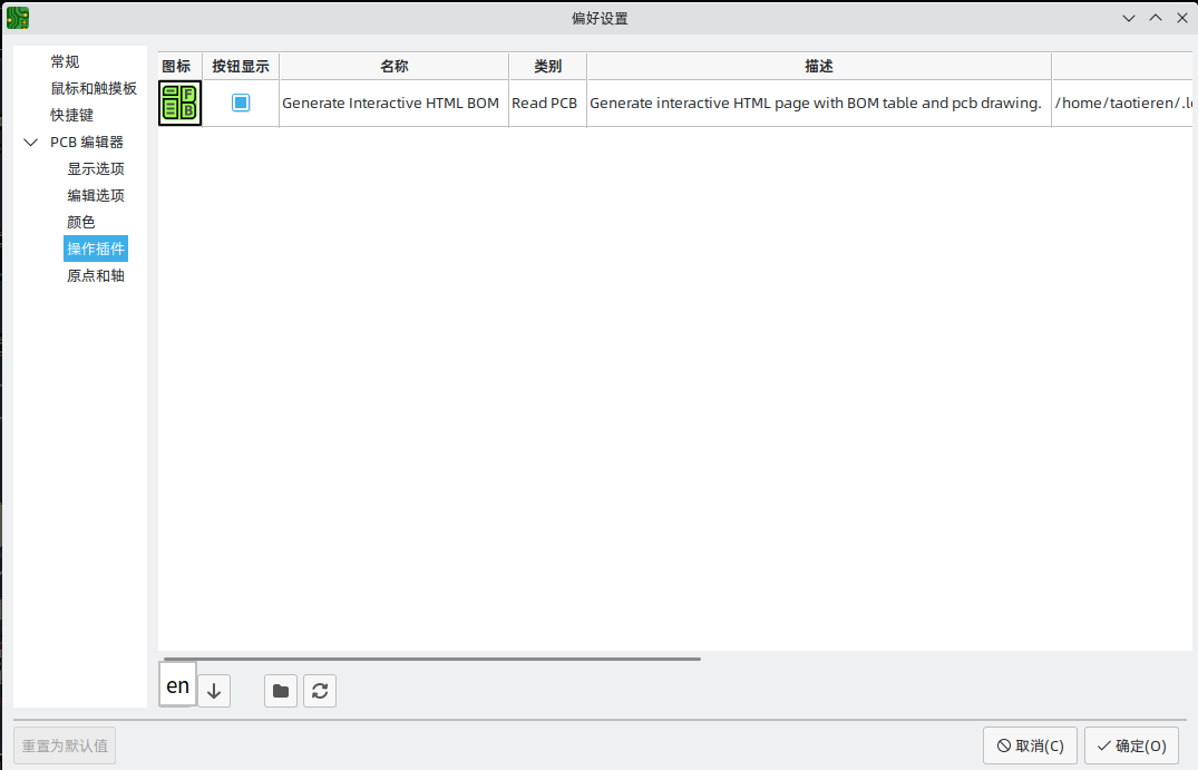
KiCad PCB 编辑器支持用 Python 编写的插件,对正在编辑的电路板进行操作。 这些插件可以使用内置的 “插件和内容管理器” 来安装(详见 KiCad 章节),或者将插件文件放在用户的插件目录中。 详见下面的脚本部分。
每个被检测到的插件都会在这个偏好设置上显示一排。 插件可以在 “PCB 编辑器” 的顶部工具栏上显示一个按钮。 如果一个插件的 "显示按钮" 控制没有被选中,它仍然可以从 "工具" > "外部插件" 菜单中访问。
列表底部的箭头控制允许改变插件在工具栏和菜单中的显示顺序。 文件夹按钮将启动一个文件资源管理器到插件文件夹,以使安装新的插件更容易。 刷新按钮将扫描插件文件夹中的任何新的或删除的插件,并更新列表。
原点和轴
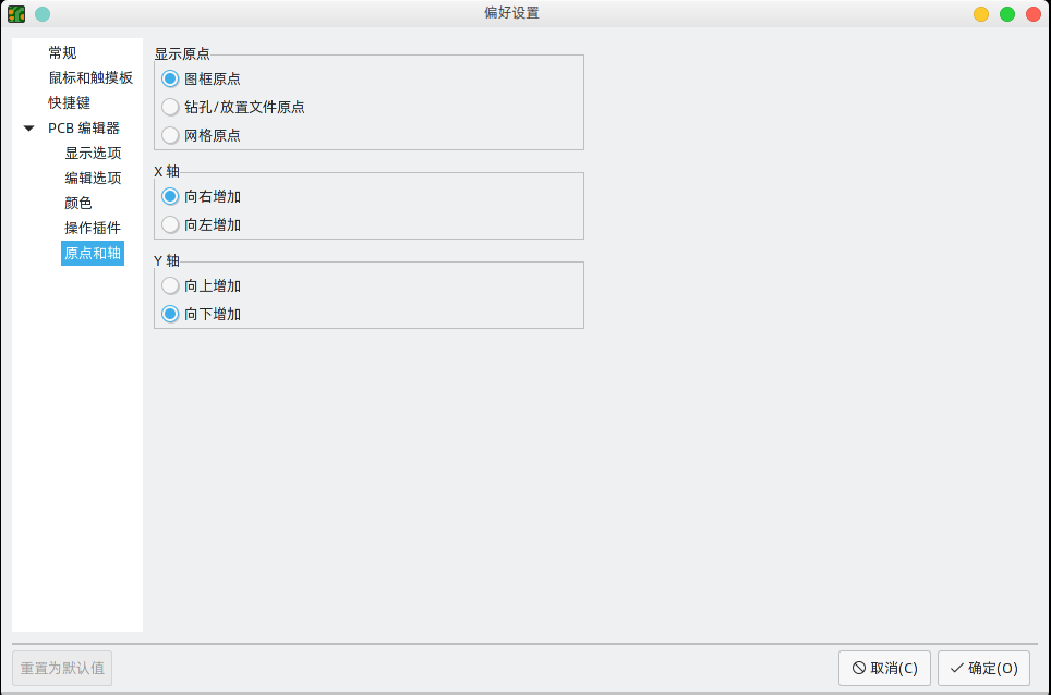
Display origin: Determines which coordinate origin is used for coordinate display in the editing canvas. The page origin is fixed at the corner of the page. The drill/place file origin and the grid origin can be moved by the user.
X axis: Controls whether X-coordinates increase to the right or to the left.
Y axis: Controls whether Y-coordinates increase upwards or downwards.
文本变量
KiCad支持文本变量,允许你用定义的文本字符串替换变量名称。 这种替换发生在变量名称在 ${VARIABLENAME} 的变量替换语法内的任何地方。
You can define project text variables in the schematic or board setup dialogs. Project text variables are defined for the whole project, so a project text variable defined in the Schematic Editor can also be used in the Board Editor.
There are also a number of built-in system text variables. System text variables may be available in some contexts and not others. The following variables can be used in PCB text, footprint text, footprint fields, and drawing sheet fields. There are also a number of variables that can be used in the Schematic Editor.
| Variable name | Description |
|---|---|
|
Contents of drawing sheet’s |
|
Contents of drawing sheet’s |
|
Today’s date, in ISO format. |
|
Filename of the board, with a file extension. |
|
Full file path of the board, with a file extension. |
|
Contents of drawing sheet’s |
|
Current version of KiCad. This variable is only available in drawing sheet fields. |
|
Layer of the object. In footprint fields and text objects in footprints, this is
the layer of the field/text object, not the layer of the parent footprint. In
drawing sheet fields, this resolves to the plotted layer, for example |
|
Current sheet’s paper size. This variable is only available in drawing sheet fields. |
|
Project name, without a file extension. |
|
Contents of drawing sheet’s |
|
Contents of drawing sheet’s |
|
Full hash of the project’s current Git commit. If the project is not part of a Git repository, resolves to "no hash". |
|
Short (8 character) hash of the project’s current Git commit. If the project is not part of a Git repository, resolves to "no hash". |
|
Contents of project text variable
|
|
Contents of footprint field Both built-in footprint fields and user-defined fields from the
corresponding symbol are available. Built-in footprint fields use all
uppercase letters: for example, to access a footprint’s value, use
Built-in footprint fields are |
|
Contents of field Both built-in footprint fields and user-defined fields from the
corresponding symbol are available. Built-in footprint fields use all
uppercase letters: for example, to access the value of Built-in footprint fields are |
|
Generates a DRC error named For example, a text item containing |
|
Generates a DRC warning named |
Custom design rules
KiCad’s custom design rule system allows creating design rules that are more specific than the generic rules available in the Constraints page of the Board Setup dialog. Custom design rules have many applications, but in general they are used to apply certain rules to a portion of the board, such as a specific net or net class, a specific area, or a specific footprint.
自定义设计规则存储在一个扩展名为 kicad_dra 的单独文件中。当您开始向项目添加自定义规则时,会自动创建此文件。如果您在项目中使用自定义规则,请在备份或提交到版本控制系统时,确保将 kicad_dra 文件与 kicad_pcb 和 kicad_pro 文件一起保存。
kicad_dra 文件由 KiCad 自动管理,不应使用外部文本编辑器进行编辑。
始终使用电路板设置对话框的自定义规则页面编辑自定义设计规则。
|
自定义规则编辑器
自定义规则编辑器位于电路板设置对话框中,它提供了一个用于输入自定义规则的文本编辑器,一个语法检查器将测试你的自定义规则并指出任何错误,还有一个语法帮助对话框,其中包含了对自定义规则语言的快速参考和一些规则示例。
The custom rules editor also provides context-sensitive autocomplete to suggest valid keywords and properties. The autocomplete suggestion menu appears automatically, but it can also be opened manually by pressing Ctrl+Space.
在编辑自定义规则后,最好使用 检查规则语法 按钮,确保没有语法错误。 自定义规则中的任何错误将阻止设计规则检查器的运行。
自定义规则语法
The custom design rule language is based on s-expressions and allows you to create design constraints that are not possible with the built-in constraints. Each design rule generally contains a condition defining what objects to match and a constraint defining the rule to be applied to the matched objects.
The language uses parentheses (( and )) to define clauses of related keywords and values. Parentheses must always be matched: for every ( there must be a matching ). Inside a clause, keywords and values are separated by whitespace (spaces, tabs, and newlines). By convention, a single space is used, but any number of whitespace characters between keywords and values is acceptable. In places where text strings are valid, strings without any whitespace may be quoted with " or ', or unquoted. Strings that contain whitespace must always be quoted. Newlines cannot be used within a quoted string. Where nested quotes are required, a single level of nesting is possible by using " for the outer quote character and ' for the inner (or vice versa). Newlines between clauses are not required, but are typically used in examples for clarity.
In the syntax descriptions below, items in <angle brackets> represent keywords or values that must be present and items in [square brackets] represent keywords or values that are optional or only sometimes required.
The Custom Rules file must start with a version header defining the version of the rules language. As of KiCad 9.0, the version is 1. The syntax of the version header is (version <number>). So in KiCad 9.0 the header should read:
(version 1)
在版本头之后,您可以输入任何数量的规则。 规则的评估顺序是相反的,也就是说,文件中的最后一条规则首先被检查。 一旦为一个给定的被测对象找到一个匹配的规则,将不再检查其他规则。在实践中,这意味着更具体的规则应该在文件的后面,以便它们在更通用的规则之前被评估。
例如,如果您创建一条规则来限制 HV 网络的布线与任何其他网络的布线之间的最小间距,然后又创建第二条规则来限制特定规则区域内所有对象的最小间距,请确保第一条规则在自定义规则文件中的出现时间比第二条规则晚,否则,如果 HV 网络中的布线落在规则区域内,可能会有错误的间距。
Each rule must have a name and one or more constraint clauses. The name can be any string and is used to refer to the rule in DRC reports. The constraint defines the behavior of the rule. Rules may also have a condition clause that determines which objects should have the rule applied, an optional layer clause which specifies which board layers the rule applies to, and an optional severity clause which specifies the severity of the resulting DRC violation.
(rule <name>
    [(severity <severity>)]
    [(layer <layer_name>)]
    [(condition <expression>)]
    (constraint <constraint_type> [constraint_arguments]))
The custom rules file may also include comments to describe rules. Comments are denoted by any line that begins with the # character (not including whitespace). You can press Ctrl+/ to comment or uncomment lines automatically.
# Clearance for 400V nets to anything else
(rule HV
    (condition "A.hasNetclass('HV')")
    (constraint clearance (min 1.5mm)))
Custom rules can reference text variables. These are not technically part of the custom rules syntax, but are resolved in a preprocessing step before evaluating the rules file. Because text variables are resolved as a simple text replacement, they can be used anywhere in the DRC rules, as long as all rules are syntactically valid after the variables have been resolved. Text variables could be used, for example, to define a project-wide value that is used in one or more constraints, like (constraint clearance (min ${hv_clearance})), where ${hv_clearance} is a text variable defined in the project as ${3 mm}.
图层子句
层 (layer) 子句确定规则将对哪些层起作用。虽然对象层可以在下面介绍的 约束 (constraint) 子句中进行测试,但是使用 层 (layer) 子句效率更高。
The value in the layer clause can be any board layer name, or the shortcut keywords outer to match the front and back copper layers (F.Cu and B.Cu) and inner to match any internal copper layers.
如果省略 层 (layer) 子句,则该规则将适用于所有层。
下面是一些示例:
# Do not allow footprints on back layer (no condition clause means this rule always applies)
(rule "Top side footprints only"
    (layer B.Cu)
    (constraint disallow footprint))

# This rule does the same thing, but is less efficient
(rule "Top side footprints only"
    (condition "A.Layer == 'B.Cu'")
    (constraint disallow footprint))

# Larger clearance on outer layers (inner layer clearance set by board minimum clearance)
(rule "clearance_outer"
    (layer outer)
    (constraint clearance (min 0.25mm)))
Severity Clause
The severity clause sets the DRC violation severity whenever the rule is violated.
Possible values are error, warning, ignore, and exclusion. Ignored rules are not observed by the interactive router and violations are not shown in the DRC dialog. However, ignored rules are evaluated for matching and therefore can still override earlier rules. Errors, warnings, and excluded rules are all observed by the interactive router, and violations are displayed in the DRC dialog when the appropriate filters are selected.
Setting a rule’s severity to ignore does not disable the rule; only the effects of the rule are disabled. The rule is still evaluated and can still override previous rules.
|
Condition Clauses
The condition clause determines which objects which objects the rule applies to. If a rule has a condition clause, the rule will apply to any objects that match the condition. If a rule does not have any condition clauses, it will apply unconditionally.
规则 条件 是一个包含在文本字符串中的表达式(因此通常用引号包围,以便允许留出空白,使之更清晰)。 该表达式是针对设计规则检查器正在测试的每一对对象进行评估的。 例如,当检查铜对象之间的间隙时,每个网络上的每个铜对象(布线段、焊盘、通孔等)都要与其他网络上的其他铜对象进行检查。 如果存在一个自定义规则,其表达式与两个给定的铜对象相匹配,并且约束条件定义了铜的间隙,那么这个自定义规则可以用来确定这两个对象之间所需的间隙。
被测对象在表达式语言中称为 A 和 B。这两个对象的顺序并不重要,因为设计规则检查器将测试这两种可能的顺序。例如,您可以编写一条规则,假设 A 为布线,B 为过孔。 有一些表达式函数可以同时测试这两个对象;这些表达式函数使用 AB 作为对象名。
The expression in a condition must resolve to a boolean value (true or false). If the expression resolves to true, the rule is applied to the given objects.
每个被测对象都有可以比较的 属性,以及可以执行特定测试的 函数。属性和函数的使用语法分别为 <object>.<property> 和 <object>.<function>([arguments])。译者注: <对象>.<属性> 和 <对象>.<函数>([参数])。
当你在文本编辑器中输入 <对象>.(A.、B. 或 AB.)时,将打开一个自动完成的列表,其中包含所有可以使用的对象属性。
|
The object properties and functions are compared using boolean and relational operators to result in a boolean expression. The following operators are supported:
|
Equal to |
|
Not equal to |
|
Greater than, greater than or equal to |
|
Less than, less than or equal to |
|
And |
|
Or |
|
Not (unary) |
For example, A.NetName == 'VDD' will apply to any objects that are part of the "VDD" net and A.NetName != B.NetName will apply to any objects that have different net names. Parentheses can be used to clarify the order of operations in complex expressions but they are not required. All the boolean operators have the same precedence and are evaluated in order from left to right.
To test a boolean property, evaluate the property itself, without comparing it to a boolean literal like true or false (which don’t exist in the DRC rules language). For example, to test if a footprint’s boolean Do_not_populate property is set, the boolean expression A.Do_not_populate by itself is sufficient. It will resolve to a true value if the footprint’s DNP attribute is set, and a false value otherwise. To check if a boolean is false, use the ! operator (unary not): !A.Do_not_populate will resolve to a true value if the DNP attribute is unset, and a false value otherwise.
有些属性表示物理测量,比如尺寸、角度、长度、位置等等。 在这些属性上,单位后缀 可以在自定义规则语言中使用,以指定使用什么单位。 如果没有使用单位后缀,属性的内部表示将被使用(距离为纳米,大多数角度为度)。 支持以下后缀:
|
Millimeters |
|
Thousandths of an inch (mils) |
|
Inches |
|
Degrees |
|
Radians |
| 自定义设计规则中使用的单位独立于 PCB 编辑器中的显示单位。 |
Numeric conditions can use simple math expressions, for example (condition "A.Hole_Size_X == 1.0mm + 0.1mm").
Constraint Clauses
The constraint clause of the rule defines the behavior of the rule on the objects that are matched by the condition. Each constraint clause has a constraint type and one or more arguments that set the behavior of the constraint. A single rule may have multiple constraint clauses, in order to set multiple constraints (for example, clearance and track_width) for objects that match the same rule conditions.
许多约束条件的参数指定了一个物理测量或数量。 这些约束条件支持最小值、最优值和最大值说明(缩写为 "min/opt/max")。 最小 和 最大 值用于设计规则检查:如果实际值小于约束条件中的最小值或大于最大值,将产生一个 DRC 错误。 最优 值仅用于某些约束,并通知 KiCad 默认使用的 "最优" 值。 例如,最优的 diff_pair_gap 是由布线器在放置新的差分对时使用的。 如果后来修改了差分对,使得差分对之间的间隙与最佳值不同,只要间隙在最小值和最大值之间(如果这些值被指定),就不会产生错误。 在所有接受最小/最大/最优值的情况下,可以指定全部的最小值、最优值和最大值。
最小/最优/最大值被指定为 (min<value>), (opt<value>), 和 (max<value>)。例如,布线宽度约束可以写成 (constraint track_width (min 0.5mm) (opt 0.5mm) (max 1.0mm)),如果只约束最小宽度,可以简单写成 (constraint track_width (min 0.5mm)) 。
Numeric constraint values can use simple math expressions, for example (constraint clearance (min 0.5mm + 0.1mm)).
| Constraint type | Argument type | Description |
|---|---|---|
|
min/opt/max |
Checks the width of annular rings on vias and pads. |
|
boolean expression |
Checks that the boolean expression is true. If the expression is false, a DRC error will be created. The expression can use any of the properties listed in the Object Properties section. |
|
Checks for solder mask bridges between copper items. This constraint does not take a min/opt/max value. In combination with a severity clause, this constraint can be used to allow or disallow solder mask bridging in various conditions. |
|
|
min |
Specifies the electrical clearance between copper objects of different nets. (See
To allow copper objects to overlap (collide), create a |
|
min |
Specifies the creepage between copper objects of different nets. |
|
min |
Checks the width of connections between pads and zones. An error will be generated for each pad
connection that is narrower than the |
|
min |
Checks the clearance between footprint courtyards and generates an error if any two courtyards
are closer than the To allow courtyard objects to overlap (collide), create a |
|
min/opt/max |
Sets the gap between parallel tracks in a differential pair. The |
|
max |
Checks the distance that a differential pair track is routed uncoupled from the other polarity
track in the pair (for example, where the pair fans out from a component, or becomes uncoupled
to pass around another object such as a via). An error will be generated for each differential
pair with an uncoupled distance that is greater than the |
|
|
Specify one or more object types to disallow, separated by spaces. For example,
|
|
min/opt/max |
Checks the clearance between objects and the board edge. This can also be thought of as the "milling tolerance" as the board edge will include all
graphical items on the To allow objects to overlap (collide) with the board edge, create an |
|
min |
Checks the clearance between a drilled hole in a pad or via and copper objects on a different net. The clearance is measured from the diameter of the hole, not its center. |
|
min/max |
Checks the size (diameter) of a drilled hole in a pad or via. For oval holes, the smaller
(minor) diameter will be tested against the |
|
min |
Checks the clearance between mechanically-drilled holes in pads and vias. The clearance is measured between the diameters of the holes, not between their centers. This constraint is solely for the protection of drill bits. The clearance between laser-drilled (microvias) and other non-mechanically-drilled holes is not checked, nor is the clearance between milled (oval-shaped) and other non-mechanically-drilled holes. |
|
min/max |
Checks the total routed length for the nets that match the rule condition and generates an
error for each net that is below the |
|
|
Checks the total number of connections (spokes) to a pad. An error will be raised for each pad that has fewer than the specified number of spokes. |
|
min |
Checks the clearance between two objects, regardless of their nets. This includes objects
with the same net and objects on non-copper layers. Only objects on physical layers and
courtyard layers are checked: this means copper, adhesive, paste, silkscreen, mask,
courtyard, and edge cut layers. Physical clearance is only checked between objects on the
same layer, except for objects on While this can perform more general-purpose checks than |
|
min |
Checks the clearance between a drilled hole in a pad or via and another object, regardless of net. The clearance is measured from the diameter of the hole, not its center. This can also be thought of as the "drilling tolerance" as it only includes round holes
(see |
|
min/opt/max |
Checks the clearance between objects on silkscreen layers and other objects. To allow silkscreen objects to overlap (collide) with other objects, create a |
|
min/opt/max/within_diff_pairs |
Checks the total skew for the nets that match the rule condition, that is, the difference
between the length of each net and the longest net that is matched
by the rule. If the difference between the longest net and the length of any one net is above
the constraint |
|
opt |
Specifies the solder mask expansion for pads, shapes and tracks. |
|
opt |
Specifies the absolute solder paste clearance for pads. Usually negative to inset the paste. The final solder paste clearance will be the absolute clearance plus the relative clearance. |
|
opt |
Specifies the relative solder paste clearance for pads. Usually negative to inset the paste. The final solder paste clearance will be the absolute clearance plus the relative clearance. |
|
min/max |
Checks the height of text, including text boxes. An error will be generated for each text item
that has a height below the |
|
min/max |
Checks the thickness of text, including text boxes. An error will be generated for each text
item that has a thickness below the |
|
min |
Specifies the width of the gap between a pad and a zone with a thermal-relief connection. |
|
opt |
Specifies the width of the spokes connecting a pad to a zone with a thermal-relief connection. |
|
min/max |
Checks the angle between two connected track segments. An error will be generated for each connected pair with an angle below the min value (if specified) or above the max value (if specified). |
|
min/max |
Checks the length of track and arc segments. An error will be generated for each segment that has a width below the min value (if specified) or above the max value (if specified). |
|
min/opt/max |
Checks the width of track and arc segments. An error will be generated for each segment that
has a width below the |
|
min/max |
Counts the number of vias on every net matched by the rule condition. An error will be generated
for each net that has fewer vias than the |
|
Checks for vias that are unconnected or connected on only one layer. This constraint does not take
a min/opt/max value. In combination with a |
|
|
min/max |
Checks the diameter of vias. An error will be generated for each via that has a diameter below
the |
|
|
Specifies the connection to be made between a zone and a pad. |
对象属性和函数参考
可以在自定义规则表达式中测试以下属性:
共有属性
这些属性适用于所有 PCB 对象。
| Property | Data type | Description |
|---|---|---|
|
string |
The board layer on which the object exists. For objects that exist on more than one layer,
this property will return the first layer (for example, |
|
boolean |
True if the object is locked. |
|
string |
Returns the unique identifier of the parent object of this object. |
|
dimension |
The position of the object’s origin in the X-axis. Note that the origin of an object is not always the same as the center of the object’s bounding box. For example, the origin of a footprint is the location of the (0, 0) coordinate of that footprint in the footprint editor, but the footprint may have been designed such that this location is not in the center of the courtyard shape. |
|
dimension |
The position of the object’s origin in the Y-axis. Note that KiCad always uses Y-coordinates that increase from the top to bottom of the screen internally, even if you have configured your settings to show the Y-coordinates increasing from bottom to top. |
|
string |
One of "Bitmap", "Dimension", "Footprint", "Graphic", "Group", "Leader", "Pad", "Target", "Text", "Text Box", "Track", "Via", or "Zone". |
连接的对象属性
这些属性适用于可以分配网络的铜对象(焊盘、过孔、敷铜、布线)。
| Property | Data type | Description |
|---|---|---|
|
integer |
The net code of the copper object. Note that net codes should not be relied upon to remain
constant: if you need to refer to a specific net in a rule, use |
|
string |
The list of all net classes for the copper object. This is a priority ordered, comma delimited list where a net has multiple net classes assigned. Note that this list may include the In an expression, an object’s
The following expressions are false, however:
You can also check if a copper object is a member of a particular net class,
regardless of any other net classes it may be a part of, using
|
|
string |
The name of the net for the copper object. Note that |
|
boolean |
True if curved edges are enabled for teardrops connected to the object. |
|
boolean |
True if teardrops are enabled for the object. |
|
boolean |
True if the "Prefer zone connections" property is set for the object. |
|
boolean |
True if the "Allow teardrops to span two tracks" property is set for the object. |
|
double |
Best ratio of teardrop length to object size for teardrops connected to the object. |
|
double |
Best ratio of teardrop width to object size for teardrops connected to the object. |
|
dimension |
Maximum length dimension for teardrops connected to the object. |
|
dimension |
Maximum width dimension for teardrops connected to the object. |
|
double |
Maximum allowable ratio of object size to track width for teardrops connected to the object. |
封装属性
这些属性适用于封装。
| Property | Data type | Description |
|---|---|---|
|
dimension |
The copper clearance override set for the footprint. |
|
string |
The name of the component class set for the footprint. This is an alphabetically ordered, comma delimited list where a footprint has multiple component classes assigned. In an expression, a footprint’s
The following expressions are false, however:
Note that while You can also check if an object is part of a footprint with a specific component class using
the |
|
boolean |
True if the footprint’s "Do not populate" attribute is set. |
|
boolean |
True if the footprint’s "Exclude from position files" attribute is set. |
|
boolean |
True if the footprint’s "Exclude from bill of materials" attribute is set. |
|
boolean |
True if the footprint’s "Exempt from courtyard requirement" attribute is set. |
|
string |
The "Keywords" from the library footprint. |
|
string |
The footprint’s description in the footprint library. This is the footprint’s
description property, not the contents of the footprint field named |
|
string |
The link to the library footprint in |
|
boolean |
True if the footprint’s "Not in schematic" attribute is set. |
|
double |
The orientation (rotation) of the footprint in degrees. |
|
string |
The reference designator of the footprint. Note that while footprints have a |
|
dimension |
The solder paste margin override set for the footprint. |
|
dimension |
The solder paste margin ratio override set for the footprint. |
|
dimension |
The thermal relief gap set for the footprint. |
|
dimension |
The thermal relief connection width set for the footprint. |
|
string |
The contents of the "Value" field of the footprint. |
|
string |
One of "Inherited", "None", "Thermal reliefs" or "Solid". |
焊盘属性
这些属性适用于封装焊盘。
| Property | Data type | Description |
|---|---|---|
|
dimension |
The copper clearance override set for the pad. |
|
string |
One of "None", "BGA pad", "Fiducial, global to board", "Fiducial, local to footprint", "Test point pad", "Heatsink pad", "Castellated pad". |
|
dimension |
The size of the pad’s drilled hole/slot in the X axis. |
|
dimension |
The size of the pad’s drilled hole/slot in the Y axis. |
|
double |
The orientation (rotation) of the pad in degrees. |
|
string |
The "number" of a pad, which can be a string (for example "A1" in a BGA). |
|
string |
One of "Circle", "Rectangle", "Oval", "Trapezoid", "Rounded rectangle", "Chamfered rectangle", or "Custom". |
|
dimension |
The value of the "pad to die length" property of a pad, which is additional length added to the pad’s net when calculating net length. |
|
string |
One of "Through-hole", "SMD", "Edge connector", or "NPTH, mechanical". |
|
string |
The name of the pad (usually the name of the corresponding pin in the schematic). |
|
string |
The electrical type of the pad (usually taken from the corresponding pin in the schematic). One of "Input", "Output", "Bidirectional", "Tri-state", "Passive", "Free", "Unspecified", "Power input", "Power output", "Open collector", "Open emitter", or "Unconnected". Pins with a no-connection flag on them will have a "+no_connect" suffix added to the pin type string. For example, "passive+no_connect" will match a passive pin with a no-connection flag. To match a pin type whether or not the pin has a no-connection flag, use a wildcard: "passive*" will match passive pins with or without a no-connection flag. |
|
double |
For rounded rectangle pads, the ratio of radius to rectangle size. |
|
dimension |
The size of the pad in the X-axis. |
|
dimension |
The size of the pad in the Y-axis. |
|
dimension |
The solder mask margin override set for the pad. |
|
dimension |
The solder paste margin override set for the pad. |
|
dimension |
The solder paste margin ratio override set for the pad. |
|
dimension |
The thermal relief gap set for the pad. |
|
dimension |
The thermal relief connection angle set for the pad. |
|
dimension |
The thermal relief connection width set for the pad. |
|
string |
One of "Inherited", "None", "Thermal reliefs" or "Solid". |
布线和圆弧属性
这些属性适用于布线和弧形布线。
| Property | Data type | Description |
|---|---|---|
|
dimension |
The x-coordinate of the start point. |
|
dimension |
The y-coordinate of the start point. |
|
dimension |
The x-coordinate of the end point. |
|
dimension |
The y-coordinate of the end point. |
|
dimension |
The width of the track or arc. |
过孔属性
这些属性适用于过孔。
| Property | Data type | Description |
|---|---|---|
|
dimension |
The diameter of the via’s pad. |
|
dimension |
The diameter of the via’s finished hole. |
|
string |
The last layer in the via stackup. |
|
string |
The first layer in the via stackup. |
|
string |
One of "Through", "Blind/buried", or "Micro". |
Tuning Pattern Properties
These properties apply to tuning patterns.
| Property | Data type | Description |
|---|---|---|
|
dimension |
The x-coordinate of the end point. |
|
dimension |
The y-coordinate of the end point. |
|
dimension |
The minimum amplitude of the tuning pattern. |
|
dimension |
The maximum amplitude of the tuning pattern. |
|
string |
One of "Single track", "Differential pair", or "Diff pair skew". |
|
string |
One of "Left", "Right", or "Default". |
|
dimension |
The minimum spacing of the tuning pattern.. |
|
integer |
The corner radius percentage of the tuning pattern. |
|
dimension |
The target length for the tuning pattern. |
|
dimension |
The target skew for the tuning pattern. |
|
boolean |
True if the tuning pattern overrides custom DRC rules. |
|
boolean |
True if the tuning pattern is single-sided. |
|
boolean |
True if the tuning pattern uses rounded meanders. |
敷铜和规则区域属性
这些属性适用于铜区和非铜区,以及规则区(以前称为禁止布线区)。
| Property | Data type | Description |
|---|---|---|
|
dimension |
The copper clearance override set for the zone. |
|
dimension |
The distance between hatched lines in the zone. |
|
float |
The minimum allowed hatching hole size, expressed as a fraction of the nominal hatching hole size. |
|
integer |
The angle (in degrees) of the hatched lines in the zone. |
|
dimension |
The width of hatched lines in the zone. |
|
dimension |
The minimum allowed width of filled areas in the zone. |
|
string |
The user-specified name (blank by default). |
|
string |
One of "Inherited", "None", "Thermal reliefs", "Solid", or "Thermal Reliefs for PTH". |
|
integer |
The priority level of the zone. |
|
dimension |
The thermal relief gap set for the zone. |
|
dimension |
The thermal relief connection width set for the zone. |
图形形状属性
这些属性适用于图形线、圆弧、圆、矩形和多边形。
| Property | Data type | Description |
|---|---|---|
|
dimension |
The angle of an arc. |
|
dimension |
The x-coordinate of the end point. |
|
dimension |
The y-coordinate of the end point. |
|
boolean |
True if the shape is filled. |
|
dimension |
Thickness of the strokes of the shape. |
|
string |
One of "Solid", "Dashed", "Dotted", "Dash-Dot", "Dash-Dot-Dot". |
|
string |
One of "Segment", "Rectangle", "Arc", "Circle", "Polygon", or "Bezier". |
|
dimension |
The x-coordinate of the start point. |
|
dimension |
The y-coordinate of the start point. |
文本属性
这些属性适用于文本对象(封装字段、自由文本标签等)。
| Property | Data type | Description |
|---|---|---|
|
boolean |
True if the text is bold. |
|
dimension |
Height of a character in the font. |
|
string |
Horizontal text justification (alignment): one of "Left", "Center", or "Right". |
|
boolean |
True if the text is italic. |
|
boolean |
True if the text has the knockout property set. |
|
boolean |
True if the text is mirrored. |
|
string |
The name of a footprint field. For text objects that are not footprint fields, this is an empty string. |
|
string |
The contents of the text object. |
|
dimension |
Thickness of the stroke of the font. |
|
dimension |
Width of a character in the font. |
|
string |
Vertical text alignment: one of "Top", "Center", or "Bottom". |
|
boolean |
True if the text object is visible (displayed). |
表达式函数
可以对自定义规则表达式中的对象调用以下函数:
| Function | Objects | Description |
|---|---|---|
|
|
Returns true if all of the object is inside the named rule area or zone. Note that
|
|
|
Returns true if the object exists on the given board layer. |
|
|
Returns true if the object exists on the copper path between the given pads. |
|
|
Returns the value of field |
|
|
Returns true if the set of component classes assigned to the object contains the named component class |
|
|
Returns true if the set of net classes assigned to the object exactly matches the named set of net
classes |
|
|
Returns true if the set of net classes assigned to the object contains the named net class |
|
|
Returns true if the object is part of a differential pair and the base name of the pair
matches the given argument |
|
|
Returns true if any part of the object is inside the named rule area or zone. Rule area and zone names can be set in their respective properties dialogs. If the given area is a filled copper zone, the function tests if the given object is inside any of the filled copper regions of the zone, not if the object is inside the zone’s outline. Deprecated; use |
|
|
Returns true if the any part of the object is inside the courtyard of the given footprint. The
first variant checks both the front or back courtyard and returns true if the object is inside
either one; the second and third variants check a courtyard on a specific layer.
The named footprint
Deprecated; use |
|
|
Returns true if any part of the object is inside the named rule area or zone. Rule area and zone names can be set in their respective properties dialogs. If the given area is a filled copper zone, the function tests if the given object is inside any of the filled copper regions of the zone, not if the object is inside the zone’s outline. |
|
|
Returns true if any part of the object is inside the courtyard of the given footprint. The
first variant checks both the front or back courtyard and returns true if the object is inside
either one; the second and third variants check a courtyard on a specific layer.
The named footprint
|
|
|
Returns true if the object is a blind/buried via. |
|
|
Returns true if the two objects being tested are part of the same differential pair but are
opposite polarities. For example, returns true if |
|
|
Returns true if the object is a microvia. |
|
|
Returns true if the object is a plated hole (in a pad or via). |
|
|
Returns true if the object is a member of the named group Deprecated; use |
|
|
Returns true if the object is a member of a group named |
|
|
Returns true if the object is a member of the given footprint.
The named footprint
|
|
|
Returns true if the object is a member of a schematic sheet named |
|
|
Returns true if the object is a member of a schematic sheet named |
自定义设计规则示例
Basic examples
(rule RF_width
    (layer outer)
    (condition "A.hasNetclass('RF')")
    (constraint track_width (min 0.35mm) (max 0.35mm)))

(rule "BGA neckdown"
    (constraint track_width (min 0.2mm) (opt 0.25mm))
    (constraint clearance (min 0.05mm) (opt 0.08mm))
    (condition "A.intersectsCourtyard('U3')"))

# Specify an optimal gap for a particular differential pair
(rule "Clock gap"
    (condition "A.inDiffPair('/CLK')")
    (constraint diff_pair_gap (opt 0.8mm)))

# Specify a larger clearance between differential pairs and anything else
(rule "Differential pair clearance"
    (condition "A.inDiffPair('*') && !AB.isCoupledDiffPair()")
    (constraint clearance (min 1.5mm)))

(rule "copper keepout"
    (constraint disallow track via zone)
    (condition "A.intersectsArea('zone3')"))

(rule "minimum creepage distance for high voltage nets"
    (condition "A.hasNetclass('HV')")
    (constraint creepage (min 5mm)))
Various clearances
(rule "Clearance between Pads of Different Nets"
    (constraint clearance (min 3.0mm))
    (condition "A.Type == 'Pad' && B.Type == 'Pad' && A.Net != B.Net"))

(rule "Pad to Track Clearance"
    (constraint clearance (min 0.2mm))
    (condition "A.Type == 'Pad' && B.Type == 'Track'"))

# Enforce a clearance around pads (and other copper objects) in a specific footprint
(rule "Pad clearance in R1"
    (constraint clearance (min 1mm))
    (condition "A.memberOfFootprint('TP1')"))

# Enforce a mechanical clearance between components and board edge
(rule front_mechanical_board_edge_clearance
    (layer "F.Courtyard")
    (constraint physical_clearance (min 3mm))
    (condition "B.Layer == 'Edge.Cuts'"))

# Prevent copper pours under capacitors
(rule "No copper pours under capacitors"
    (constraint physical_clearance (min 0.1mm))
    (condition "A.Type == 'Zone' && B.Reference == 'C*'")
)

# This assumes that there is a cutout with 1mm thick lines
(rule "Clearance to cutout"
    (constraint edge_clearance (min 0.8mm))
    (condition "A.Layer=='Edge.Cuts' && A.Line_Width == 1.0mm"))

# prevent silk over tented vias
(rule silk_over_via
    (constraint silk_clearance (min 0.2mm))
    (condition "A.Type == '*Text' && B.Type == 'Via'"))

(rule "Allow connector silk to intersect board edge"
    (constraint silk_clearance)
    (severity ignore)
    (condition "A.memberOfFootprint('J*') && B.Layer=='Edge.Cuts'"))

(rule "Distance between Vias of Different Nets"
    (constraint hole_to_hole (min 0.254mm))
    (condition "A.Type == 'Via' && B.Type == 'Via' && A.Net != B.Net"))

(rule "Via Hole to Track Clearance"
    (constraint hole_clearance (min 0.254mm))
    (condition "A.Type == 'Via' && B.Type == 'Track'"))

(rule "Distance between test points"
    (constraint courtyard_clearance (min 1.5mm))
    (condition "A.Reference =='TP*' && B.Reference == 'TP*"))
High-current design rules
# Check current-carrying capacity
(rule high-current
    (constraint track_width (min 1.0mm))
    (constraint connection_width (min 0.8mm))
    (condition "A.hasNetclass('Power')"))

# Don't use thermal reliefs on heatsink pads
(rule heat_sink_pad
    (constraint zone_connection solid)
    (condition "A.Fabrication_Property == 'Heatsink pad'"))

# Require all four thermal relief spokes to connect to parent zone
(rule fully_spoked_pads
    (constraint min_resolved_spokes 4))

# Set thermal relief gap & spoke width for all zones
(rule defined_relief
    (constraint thermal_relief_gap (min 10mil))
    (constraint thermal_spoke_width (min 12mil)))

# Override thermal relief gap & spoke width for GND and PWR zones
(rule defined_relief_pwr
    (constraint thermal_relief_gap (min 10mil))
    (constraint thermal_spoke_width (min 12mil))
    (condition "A.Name == 'zone_GND' || A.Name == 'zone_PWR'"))

# Prevent solder wicking from SMD pads
(rule holes_in_pads
    (constraint physical_hole_clearance (min 0.2mm))
    (condition "B.Pad_Type == 'SMD'"))

# Disallow solder mask margin overrides
(rule "disallow solder mask margin overrides"
    (constraint assertion "A.Soldermask_Margin_Override == 0mm")
    (condition "A.Type == 'Pad'"))
Hole sizes
(rule "Max Drill Hole Size Mechanical"
    (constraint hole_size (max 6.3mm))
    (condition "A.Pad_Type == 'NPTH, mechanical'"))

(rule "Max Drill Hole Size PTH"
    (constraint hole_size (max 6.35mm))
    (condition "A.Pad_Type == 'Through-hole'"))

# Separate drill bit and milling cutter size constraints
(rule "Plated through-hole size"
    (constraint hole_size (min 0.2mm) (max 6.35mm))
    (condition "A.isPlated() && A.Hole_Size_X == A.Hole_Size_Y"))

(rule "Plated slot size"
    (constraint hole_size (min 0.5mm))
    (condition "A.isPlated() && A.Hole_Size_X != A.Hole_Size_Y"))
Solder mask and solder paste
# No solder mask expansion for vias
(rule "no mask expansion on vias"
    (constraint solder_mask_expansion (opt 0mm))
    (condition "A.type == via"))


# Remove solder paste from DNP footprints
(rule remove_solder_paste_from_DNP
    (constraint solder_paste_abs_margin (opt -50mm))
    (condition "A.Do_not_Populate"))

# Allow solder mask bridging under guard ring mask apertures
(rule guard_ring_bridging
    (constraint bridged_mask)
    (condition "A.intersectsArea('guard_ring')")
    (severity ignore))
Dangling vias
# allow dangling vias within a specific rule area named 'dangling vias allowed'
(rule ignore_left
    (constraint via_dangling)
    (condition "A.enclosedByArea('dangling vias allowed')")
    (severity ignore))
脚本
Scripting allows you to automate tasks within KiCad using the Python language. KiCad provides an API for editing PCBs that can be used interactively or in standalone scripts. Board Editor scripts can be organized as "action plugins", which are displayed as icons in the top toolbar of the Board Editor. There is also a separate Footprint Wizard API that can be used to create footprint creation plugins for the Footprint Editor.
This manual covers general scripting concepts for the Board Editor’s pcbnew API as well as for the footprint wizard API. Users wishing to write or modify scripts should also use the Doxygen documentation for these APIs located at https://docs.kicad.org/doxygen-python-nightly/namespaces.html.
KiCad 6 或更新版本需要 Python 3 来支持脚本。Python 2 已不再被支持。
使用脚本控制台
PCB 编辑器带有一个内置的 Python 控制台,可以用来检查并与电路板互动。 要启动控制台,使用顶部工具栏中的 ![]() 按钮。PCB 编辑器的 Python API 不会自动加载,所以要加载它,在控制台中输入
按钮。PCB 编辑器的 Python API 不会自动加载,所以要加载它,在控制台中输入 import pcbnew。然后 pcbnew.GetBoard() 命令将返回当前在 PCB 编辑器中加载的电路板的引用,可以通过控制台进行检查和修改。
Python 脚本位置
Plugin scripts (PCB action plugins and footprint wizards) can be installed automatically using the Plugin and Content Manager (PCM), or manually by copying the plugin to a folder. Manually installed plugins should each be in their own folder within the plugins folder. The location of the plugins folder is by default:
| Platform | Path |
|---|---|
Linx |
|
macOS |
|
Windows |
|
The type of plugin is determined by the Python class it inherits from. Inheriting from
FootprintWizardBase.FootprintWizard will create a footprint wizard plugin, and inheriting from
pcbnew.ActionPlugin will create an action plugin. Creating action plugins and footprint wizards
is described in more detail below.
|
pcbnew API overview
The scripting API reflects the internal object structure inside KiCad’s Board Editor. It is provided by the pcbnew module in Python.
| Because the API is tightly coupled to KiCad’s internals, the API will change over time and is not considered stable. Consult the doxygen documentation for the most up-to-date API reference, and be sure to use the documentation for the appropriate version of KiCad. |
Scripts, action plugins, and interactive scripting sessions often start with a call to GetBoard(), which returns a BOARD object representing the currently open board and its contents.
BOARD has a set of properties and a set for each type of object in the board: footprints, zones, tracks, vias, text, etc. Each type of object has its own properties and holds its own objects: a footprint will likely have at least one pad, for example.
The objects in the BOARD can be accessed using methods that each return an iterable list of the corresponding object type. A selection of these methods are listed below. Other methods are listed in the doxygen documentation.
-
board.GetFootprints(): returns a list of all of the footprints in the board. -
board.GetDrawings(): returns a list of miscellaneous board objects in the board. -
board.GetTracks(): returns a list of all of the tracks and vias in the board. -
board.GetZones(): returns a list of all of the zones in the board. -
board.GetNetClasses():returns a list of all net classes in the board’s design rules.
Boards can be loaded and saved from disk using the following functions:
-
LoadBoard(filename): loads a board from file, returning aBOARDobject, using the file format that matches the filename extension. -
SaveBoard(filename, board): saves aBOARDobject to file, using the file format that matches the filename extension. -
board.Save(filename): the same asSaveBoard(), but a method of theBOARDobject.
例子
Load a board, hide all values, and show all references.
#!/usr/bin/env python3
import sys
from pcbnew import LoadBoard

filename = sys.argv[1]

pcb = LoadBoard(filename)
for fp in pcb.GetFootprints():
    print(f"* Footprint: {fp.GetReference()}")
    fp.Value().SetVisible(False)      # set Value as Hidden
    fp.Reference().SetVisible(True)   # set Reference as Visible

pcb.Save("mod_" + filename)
Change the paste mask margin for pins 1-14 of a footprint.
#!/usr/bin/env python3
import sys
from pcbnew import *

filename=sys.argv[1]
pcb = LoadBoard(filename)

# Find module U304
u304 = pcb.FindFootprintByReference('U304')
pads = u304.Pads()

#  Iterate over pads, printing solder paste margin
for p in pads:
    print(p.GetPadName(), ToMM(p.GetLocalSolderPasteMargin()))
    id = int(p.GetPadName())
    # Set margin to 0 for all but pad (pin) 15
    if id<15: p.SetLocalSolderPasteMargin(0)

pcb.Save("mod_"+filename)
Load a footprint library, list footprints in the library, and list pads in each footprint.
#!/usr/bin/env python3
from pcbnew import *

libpath = "/usr/share/kicad/footprints/Connector_PinSocket_2.54mm.pretty"
print(f">> enumerate footprints, pads of {libpath}")

# Load the suitable plugin to read/write the .pretty library
src_type = PCB_IO_MGR.GuessPluginTypeFromLibPath( libpath );
# We can force the plugin type by using IO_MGR.PluginFind( IO_MGR.KICAD )
plugin = PCB_IO_MGR.PluginFind( src_type )

# Print plugin type name: (Expecting "KiCad" for a .pretty library)
print(f"Selected plugin type: {PCB_IO_MGR.ShowType(src_type)}")

list_of_footprints = plugin.FootprintEnumerate(libpath)

for name in list_of_footprints:
    fp = plugin.FootprintLoad(libpath,name)
    # print the short name of the footprint
    print(name)
    # followed by ref field, value field, and decription string:
    # Remember ref and value texts are dummy text, replaced by the schematic values
    # when reading a netlist.
    print(f"  -> {fp.GetReference()} {fp.GetValue()} {fp.GetLibDescription()}")
    for pad in fp.Pads():
        print(
            f"    pad [{pad.GetPadName()}] at "
            f"pos ({ToMM(pad.GetPosition().x)}, {ToMM(pad.GetPosition().y)}) mm,",
            f"shape offset ({ToMM(pad.GetOffset().x)}, {ToMM(pad.GetOffset().y)}) mm"
        )
    print()
Load a board and print information about each item in the board.
#!/usr/bin/env python
import sys
from pcbnew import *

filename=sys.argv[1]
pcb = LoadBoard(filename)

print("Listing Tracks and Vias:")
for item in pcb.GetTracks():
    if type(item) is PCB_VIA:
        pos = item.GetPosition()
        drill = item.GetDrillValue()
        width = item.GetWidth()
        print(f" * Via:   {ToMM(pos)} - {ToMM(drill)}/{ToMM(width)}")
    elif type(item) is PCB_TRACK:
        start = item.GetStart()
        end = item.GetEnd()
        width = item.GetWidth()
        print(f" * Track: {ToMM(start)} to {ToMM(end)}, width {ToMM(width)}")
    else:
        print(f"Unknown type    {type(item)}")

print()
print("Listing Text and Shapes:")
for item in pcb.GetDrawings():
    if type(item) is PCB_TEXT:
        print(f"* Text:    '{item.GetText()}' at {ToMM(item.GetPosition())}")
    elif type(item) is PCB_SHAPE:
        print(f"* Drawing: {item.GetShapeStr()}")
    else:
        print(f"Unknown type    {type(item)}")

print()
print("Listing Footprints")
for fp in pcb.GetFootprints():
    print(f"* Footprint: {fp.GetReference()} at {ToMM(fp.GetPosition())}")

print()
print(f"Ratsnest count: {pcb.GetNetCount()}")
print(f"Track width count: {len(pcb.GetTrackWidthList())}")
print(f"Via size count: {len(pcb.GetViasDimensionsList())}")

print()
print(f"Listing Zones: {pcb.GetAreaCount()}")
for idx in range(0, pcb.GetAreaCount()):
    zone = pcb.GetArea(idx)
    print(f"zone: {idx} priority: {zone.GetAssignedPriority()} netname: {zone.GetNetname()}")

print()
print(f"Netclasses: {len(pcb.GetAllNetClasses())}")
操作插件
Action plugin associate a script with a button in the PCB Editor GUI. Clicking the button runs the script. Action plugins are shown in the Tools → External plugins menu, and can also be shown in the toolbar if enabled in the Action Plugins page of the Preferences dialog.
The example below is an action plugin that uses KiCad’s pcbnew API to replace the string $date$ with the current date in any text item.
import pcbnew
import re
import datetime

class text_by_date(pcbnew.ActionPlugin):
    """
    test_by_date: A sample plugin as an example of ActionPlugin
    Add the date to any text field of the board containing '$date$'
    How to use:
    - Add a text on your board with the content '$date$'
    - Call the plugin
    - The text will automatically be updated with the date (format YYYY-MM-DD)
    """

    def defaults(self):
        """
        Method defaults must be redefined
        self.name should be the menu label to use
        self.category should be the category (not yet used)
        self.description should be a comprehensive description
          of the plugin
        """
        self.name = "Add date on PCB"
        self.category = "Modify PCB"
        self.description = "Automatically add date on an existing PCB"

    def Run(self):
        pcb = pcbnew.GetBoard()
        for item in pcb.GetDrawings():
            if item.GetClass() == "PCB_TEXT":
                txt = re.sub("\$date\$ [0-9]{4}-[0-9]{2}-[0-9]{2}",
                                 "$date$", item.GetText())
                if txt == "$date$":
                    item.SetText("$date$ %s" % datetime.date.today())


text_by_date().register()
封装向导
Footprint wizards are Python scripts that can be accessed from the Footprint Editor. Each footprint wizard presents a selection of parameters defined in the Python script, and creates a footprint based on the parameter values.
There are 3 minimum steps required to create a footprint wizard, which are described below. For examples of how to create footprint wizards, see the footprint wizards included with KiCad.
-
Instantiate a Python class, inheriting from
FootprintWizardBase.FootprintWizard. -
Define the 6 required functions:
GetName(),GetDescription(),GetValue(),GenerateParameterList(),CheckParameters(), andBuildThisFootprint(). -
Register the class by calling
{your_class_name}().register().
The GetName(), GetDescription(), and GetValue() functions are there to provide strings to the UI. The only functionality needed is to return an appropriate string.
The GenerateParameterList() function defines the parameters needed for the footprint. Parameters are grouped into a page + name format. For example, calling self.AddParam("demo", "radius", self.uMM, 5) would add a parameter named radius into the page named demo. Retrieving that parameter data would be done with a call such as self.footprint_radius = self.parameters["demo"]["radius"].
The CheckParameters() function is available to perform any data validation on the parameters defined in GenerateParameterList(). This function is also where the self.footprint_radius = self.parameters["demo"]["radius"] calls reside.
The BuildThisFootprint() function is where the footprint building steps are called. This function is where one creates the footprint.
The required {your_class_name}().register() call can either be at the end of the Python file, or in an __init__.py file. Both styles are supported by KiCad.
KiCad will not reload a plugin after it has raised an error (for example, the NotImplementedError).
One will need completely close out KiCad and restart it. However, this doesn’t apply to changes
which do not raise an error.
|
IDF component outlines
KiCad 可以 [IDF 导出器,导出电路板的 IDF 表示],以便在机械 CAD 软件中使用。下面是一些关于将 IDF 元件边框附在封装上、创建新的 IDF 元件边框的指导,以及 KiCad 中包含的 IDF 工具的描述。
指定供导出程序使用的元件模型
IDF component models are attached to footprints using the footprint’s 3D model properties. The IDF exporter uses different filetypes than the 3D viewer and other 3D model exporters, so adding 3D models for the IDF exporter does not conflict with 3D models added to a footprint for other purposes.
要在封装或 PCB 编辑器中把 IDF 模型添加到封装中,编辑封装的属性并点击 3D 模型标签。
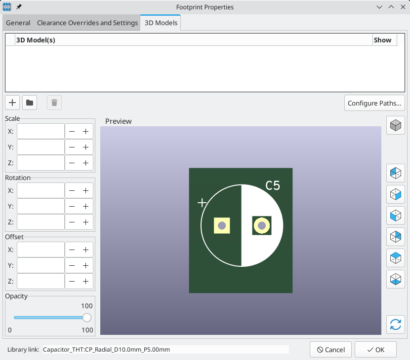
点击 ![]() 按钮,选择 IDF(*.idf;*.IDF) 文件类型筛选器。浏览到所需的边框文件。
按钮,选择 IDF(*.idf;*.IDF) 文件类型筛选器。浏览到所需的边框文件。
一旦选择了所需的元件边框文件,输入任何必要的偏移和旋转值。偏移量必须使用 IDF 板的输出单位(毫米或mil)并在 IDF 坐标系中指定,这是一个右手坐标系,+Z 指向观察者,+X 指向观察者的右边,+Y 指向屏幕的上边缘。旋转必须以度为单位;正向旋转是逆时针旋转,如 IDF v3 规范中所述。
多个边框可以与适当的偏移量结合起来,以表示简单的装配,如插座中的 DIP 封装。
| IDF 导出器只使用偏移值和 Z 旋转值,所有其他数值都被忽略。 |
创建元件边框文件
元件边框文件(*.idf)包括一个单一的 .ELECTRICAL 或 .MECHANICAL 部分,如规范文件中所述。该部分前面可以有任何数量的注释行;注释行由导出器复制到库文件中,可以用来跟踪元数据,如用于确定元件边框和尺寸的文件的参考。
元件边框部分包含字符串,整数或浮点数字段。 字符串是可包含空格的字符组合; 如果字符串包含空格,则必须引用它。 引号不得出现在字符串中。 浮点数可以使用十进制或指数表示法表示,但十进制表示法是人类可读性的首选。 小数点必须是点而不是逗号。 IDF 文件必须只包含7位 ASCII 字符; 使用8位字符将导致未定义的行为。
IDF 文件由 SECTIONS 组成,SECTIONS 由 RECORDS(记录) 组成,RECORDS 由 FIELDS(字段) 组成。对于 IDF 边框文件,只有一种类型的部分可以存在,并且必须是 .ELECTRICAL 或 .MECHANICAL 中的一种。一个记录是一行文本,可能包含一个或多个字段。字段是由一个或多个空格分隔的字符序列,不在引号之间出现。一条记录的所有字段必须出现在单行上;记录不能跨行。
Section的标题(.ELECTRICAL 或 .MECHANICAL)被认为是该节的第一条记录(记录 1)。记录 1 后面必须有记录 2,该记录有四个字段:
-
几何名称:与元件编号组合的字符串必须形成元件边框的唯一标识符。 对于标准化的封装,封装名称是几何名称的一个很好的值,例如 "SOT-23"。对于独特的封装,制造商的元件编号是几何名称的一个好选择。
-
元件编号:虽然明显是为了零件号,例如BS107,但最好使用这个字符串来帮助描述封装。 例如,如果几何名称是 "TO-92",则零件号条目可用于描述焊盘的布局或该特定 TO-92 边框文件的方向。
-
IDF 单位:必须是
MM或THOU中的一个,它只适用于描述这个单一元件边框的单位。 -
高度:这是一个浮点数,代表元件的名义高度,使用字段 3 中指定的单位。
记录 2 后面必须跟有许多记录 3 条目,这些条目指定了元件的边框。 记录 3 包含四个字段:
-
循环索引。
0(边框点按逆时针顺序指定)或1(边框点按顺时针顺序指定)。 -
X 坐标:浮点数
-
Y 坐标:浮点数
-
包括角度:一个浮点数。如果该值为
0,则从上一点到这一点绘制一条直线段。 如果数值是360,那么前一个点指定一个圆的中心,这个点指定圆上的一个点;千万不要用360的数值指定一个圆,因为至少有一个主要的机械 CAD 包在这种情况下表现不好。如果该值为负数,则从上一点到这一点将绘制顺时针方向的圆弧;如果该值为正数,则绘制逆时针方向的圆弧。
只允许一个闭环,并且无法指定切口。 指定的最后一个点必须与第一个点相同,除非边框是圆形。
示例 IDF 文件 1:
# a simple cylinder - this could represent an electrolytic capacitor
.ELECTRICAL
    "cylinder" "5mm OD, 5mm height" MM 5
    0 0 0 0
    0 2.5 0 360
.END_ELECTRICAL
示例 IDF 文件 2:
# an upside-down T
# a comment added for the sake of adding comments
.ELECTRICAL
    "Capital T" "5x8x10mm, upside down" MM 10
    0 -0.5 8 0
    0 -0.5 0.5 0
    0 -2.5 0.5 0
    0 -2.5 -0.5 180
    0 2.5 -0.5 0
    0 2.5 0.5 180
    0 0.5 0.5 0
    0 0.5 8 0
    0 -0.5 8 180
.END_ELECTRICAL
创建边框的准则
在创建边框时,特别是在与他人共享工作时,文件的设计和命名的一致性可以帮助人们更快地找到文件并以最小的麻烦放置元件。
封装命名
尽量在文件名中提供一些关于边框的信息,让用户对边框有一个大致的概念。 例如,轴向引线圆柱形封装可能代表某些类型的电容器以及某些类型的电阻,因此将边框识别为水平或垂直轴向引线器件并在相关尺寸上添加一些额外信息是有意义的:直径,长度 和间距是最重要的。 如果元件具有独特的边框,制造商的零件编号和一个前缀来表明元件的类别就足够了。
注释
使用 IDF 文件中的注释为用户提供有关边框的更多信息,例如对用于尺寸信息的源的引用。
几何形状和零件编号条目
仔细考虑要赋予几何形状和零件编号条目的值。 总之,这些字符串作为 MCAD 系统的唯一标识符。 理想情况下,字符串的值对用户有一定的意义,但这不是必需的:这些值主要用于 MCAD 系统用作唯一 ID。 理想情况下,所选择的值在任何大型边框集合中都是唯一的; 选择好的值将导致更少的冲突,特别是在复杂的电路板上。
引脚方向和定位
元件边框的创建应该与相应的封装的方向和位置相匹配。这就避免了为 IDF 元件边框指定非零旋转的需要。由于 IDF 导出器忽略了 (X,Y) 偏移值,所以在 IDF 元件边框中使用正确的原点是至关重要的。
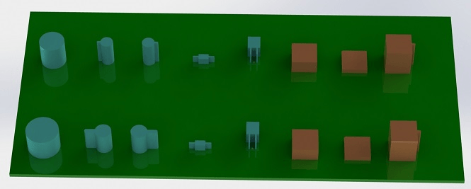
上图显示了由程序 idfcyl 和 idfrect 生成并在一个机械 CAD 程序中渲染的样本边框。从左到右分别是 (a) 垂直径向引线圆柱体,(b) 垂直轴向引线圆柱体,左边有线路,(c) 垂直轴向引线圆柱体,右边有线路,(d) 水平轴向引线圆柱体,(e) 水平径向引线圆柱体,(f) 方形边框,普通,(g) 方形边框有倒角,(h) 方形边框有轴向引线在右边。上面的边框以毫米为单位,下面的边框以英寸为单位。
尺寸提示
拉伸边框的目的是让机械设计者了解每个元件占据的位置和物理空间。在典型情况下,机械设计师将使用更详细的机械模型替换一些粗略边框,例如在检查时确保直角安装的 LED 适合面板上的孔。在大多数情况下,边框的准确性无关紧要,但好的做法是创建可传达最佳机械信息的边框。在少数情况下,用户可能希望将元件装配到空间很小的壳体中,例如装进一个便携式音乐播放器中。在这种情况下,如果大多数拉伸边框是元件的足够好的表示,那么机械设计师可能只需要在设计壳体时替换很少的模型。如果边框不是现实的可靠反映,那么机械设计师将浪费大量时间来更换模型以确保良好的配合。毕竟,如果你把垃圾放进去,你可以预期会有垃圾出来。如果您提供了良好的信息,您可以对良好的结果充满信心。
IDF 元件边框工具
许多命令行工具可用于帮助生成 IDF 元件边框。 工具是:
-
idfcyl:创建一个垂直或水平方向的圆柱体边框,并具有轴向或径向引线 -
idfrect:创建一个矩形的边框,这个矩形可以有一个轴向引线或左上角的倒角 -
dxf2idf:将 DXF 格式的图纸转换为 IDF 元件边框
idfcyl
idfcyl 生成圆柱形元件的边框。
当 idfcyl 被调用时,没有参数,它会打印出一个使用说明和输入的摘要:
idfcyl:该程序生成圆柱形元件的边框。
     圆柱体可以是水平的或垂直的。
     水平圆柱体可以在一端或两端有导线。
     垂直圆柱体最多可以有一条导线
     放在左侧或右侧。

输入:
    单位:mm, in(毫米或英寸)
    方向:V(垂直)
    引线类型:X,R(轴向,径向)
    柱体直径
    柱体长度
    板偏移
    *   导线直径
    *   间距
    **  线侧:L,R(左,右)
    *** 引线长度
    文件名(必须以 * .idf 结尾)

    注意:
         *   仅用于水平方向或
             带轴向引线的垂直方向

        **  只有轴向引线的垂直方向才需要

        ***  仅对于带有径向引线的水平方向需要
可以通过在命令行上输入任意参数来抑制注释。 用户可以在命令行手动输入信息或创建脚本以生成边框。 以下脚本创建一个单圆柱轴向引线边框,右侧为引线:
#!/bin/bash
# Generate a cylindrical IDF outline for test purposes
# vertical 5mm cylinder,  nominal length 8mm + 3mm board offset,
# axial wire on right,  0.8mm wire dia., 3.5mm pitch
idfcyl - 1 > /dev/null <<  _EOF
mm
v
x
5
8
3
0.8
3.5
r
cylvmm_1R_D5_L8_Z3_WD0.8_P3.5.idf
_EOF
idfrect
idfrect 生成矩形元件的边框。
当 idfrect 被调用而没有参数时,它会打印出使用说明和输入摘要:
idfrect:该程序生成矩形元件的边框。
     该元件可能有有单引线(轴向)或左上角
     有倒角。
输入:
     单位:毫米,英寸(毫米或英寸)
     宽度:
     长度:
     高度:
     倒角:45 度倒角的长度
     * 引线:Y,N(引线始终向右边)
     ** 导线直径
     ** 间距
     文件名(必须以 *.idf 结尾)

    注意:
        *   仅当倒角 = 0 时才需要

        **  仅对有引线的元件有要求
可以通过在命令行上输入任意参数来抑制注释。 用户可以在命令行手动输入信息或创建脚本以生成边框。 以下脚本创建倒角矩形和轴向引线边框:
#!/bin/bash
# Generate various rectangular IDF outlines for test purposes
# 10x10, 1mm chamfer, 2mm height
idfrect - 1 > /dev/null <<  _EOF
mm
10
10
2
1
rectMM_10x10x2_C0.5.idf
_EOF
# 10x10x12,  0.8mm lead on 6mm pitch
idfrect - 1 > /dev/null <<  _EOF
mm
10
10
12
0
Y
0.8
6
rectLMM_10x10x12_D0.8_P6.0.idf
_EOF
dxf2idf
dxf2idf 从 DXF 边框创建一个 IDF 元件文件。
用于指定元件边框的 DXF 文件可以用免费软件 LibreCAD 来准备,以获得最佳的兼容性。
当 dxf2idf 被调用而没有参数时,它会打印出一个使用说明和输入的摘要:
dxf2idf:该程序从 DXF 文件中获取线段、圆弧段和圆段,并创建 IDF 元件边框文件。

输入:
     DXF 文件名:输入文件,必须以 '.dxf' 结尾
     单位:毫米,英寸(毫米或英寸)
     几何名称:字符串,根据 IDF 3.0版规范
     元件名称:根据元件号的 IDF 3.0版规范
     高度:边框的拉升高度
     注释:所有非空行都是要添加到IDF 文件
         的注释。 空行表示注释块
         结束。
     文件名:输出文件名,必须以 '.idf' 结尾
可以通过在命令行上输入任何任意参数来抑制注释的产生。用户可以在命令行上手动输入信息或创建脚本来生成边框。下面的脚本从 DXF 文件 test.dxf 创建了一个 5 毫米高的边框:
#!/bin/bash
# Generate an IDF outlines from a DXF file
dxf2idf - 1 > /dev/null << _EOF
test.dxf
mm
DXF TEST GEOMETRY
DXF TEST PART
5
This is an IDF test file produced from the outline 'test.dxf'
This is a second IDF comment to demonstrate multiple comments

test_dxf2idf.idf
_EOF
idf2vrml
idf2vrml 工具读取一组 IDF 板(.emn)和一个 IDF 元件文件(.emp)并产生一个 VRML 文件,可以用 VRML 查看器查看。在用户不能使用 MCAD 软件的情况下,这个功能对板件装配的可视化很有用。在没有任何参数的情况下调用 idf2vrml 将导致显示用发消息:
>./idf2vrml
用法: idf2vrml -f input_file.emn -s scale_factor {-k} {-d} {-z} {-d} {-z} {-m}
标志:
   -k: 产生 KiCad 友好的 VRML 输出;默认为紧凑的 VRML
   -d: 抑制对默认边框的替换
   -z: 抑制零高度边框的渲染
   -m: 打印对象映射到标准输出进行调试。
例子产生一个供 KiCad 使用的模型: idf2vrml -f input.emn -s 0.3937008 -k
idf2vrml 工具不能正确渲染 emn 文件中的 OTHER_OUTLINE 实体,如果该实体被指定在 PCB 的底层;然而你不会注意到使用 KiCad 导出的文件,因为没有机制来指定这样的实体。这如果您渲染的第三方 emn 文件确实在电路板的背面使用了实体,那么这只是一个问题。
|