原理图创建和编辑
简介
用 KiCad 设计的原理图不仅仅是一个电子设备的简单图形表示。它通常是开发链的切入点,可用于:
-
根据一套规则(《ERC,电气规则检查》)进行验证,以发现错误和遗漏。
-
自动生成《创建自定义的网表和 BOM 文件,材料清单》。
-
《创建自定义网表和 BOM 文件,生成网表》用于仿真软件,如 SPICE。
-
《创建自定义的网表和 BOM 文件,定义电路》,用于转移到 PCB 布局。
原理图主要由符号、导线、标签、结点、总线和电源符号组成。为了使原理图更清晰,你可以放置纯图形元素,如总线入口、注释和折线。
符号是从符号库中添加到原理图中的。原理图制作完成后,连接和封装的集合被导入 PCB 编辑器,用于设计电路板。
原理图可以包含在一个原理图中,也可以分割成多个原理图。在 KiCad 中,多张原理图是按层次组织的,有一个根原理图和子原理图。每个原理图都是它自己的 .kicad_sch 文件,它本身就是一个完整的 KiCad 原理图。层次原理图的工作在《层次原理图,层次原理图》章节中描述。
原理图编辑操作
原理图编辑工具位于右边的工具栏中。 当一个工具被激活时,它将一直处于活动状态,直到选择了另一个工具或用 Esc 键取消该工具。当任何其他工具被取消时,选择工具总是被激活。
|
Selection tool (the default tool) |
|
Highlight a net by marking its wires and net labels with a different color. If the PCB Editor is also open then copper corresponding to the selected net will be highlighted as well. Net highlighting can be cleared by clicking with the highlight tool in an empty space, or by using the Clear Net Highlighting hotkey (~). |
|
Display the symbol selector dialog to place a new symbol. |
|
Display the power symbol selector dialog to place a new power symbol. |
|
Draw a wire. |
|
Draw a bus. |
|
Draw wire-to-bus entry points. These elements are only graphical and do not create a connection, thus they should not be used to connect wires together. |
|
Place a "no-connection" flag. These flags should be placed on symbol pins which are meant to be left unconnected. "No-connection" flags indicate to the Electrical Rule Checker that the pin is intentionally unconnected and not an error. |
|
Place a junction. This connects two crossing wires or a wire and a pin, which can sometimes be ambiguous without a junction (i.e. if a wire end or a pin is not directly connected to another wire end). |
|
Place a local label. Local labels connect items located in the same sheet. For connections between two different sheets, use global or hierarchical labels. |
|
Place a net class directive label. |
|
Place a global label. All global labels with the same name are connected, even when located on different sheets. |
|
Place a hierarchical label. Hierarchical labels are used to create a connection between a subsheet and the sheet’s parent sheet. See the Hierarchical Schematics section for more information about hierarchical labels, sheets, and pins. |
|
Place a hierarchical subsheet. You must specify the file name for this subsheet. |
|
Import a hierarchical pin from a subsheet. This command can be executed only on hierarchical subsheets. It will create hierarchical pins corresponding to hierarchical labels placed in the target subsheet. |
|
Place a text comment. |
|
Place a text box. |
|
Draw a rectangle. |
|
Draw a circle. |
|
Draw an arc. |
|
Draw lines. Note: Lines are graphical objects and are not the same as wires placed with the Wire tool. They do not connect anything. |
|
Place a bitmap image. |
|
Delete clicked items. |
网格
在原理图编辑器中,光标总是在一个网格上移动。该网格可以自定义:
-
尺寸可以通过右键菜单或使用 视图 → 网格属性… 来改变。
-
颜色可以在 偏好设置 对话框的 颜色 页中改变(菜单 偏好设置 → 常规选项)。
-
可见性可以通过左侧的工具栏按钮进行切换。
默认的网格尺寸是 50 mil(0.050 英寸)或 1.27 mm。
这是推荐的网格,用于在原理图中放置符号和导线,以及在符号编辑器中设计符号时放置引脚。
| 导线只有在两端完全重合的情况下才能与其他导线或引脚连接。因此,保持符号引脚和导线与网格对齐是非常重要的。建议在放置符号和绘制导线时始终使用 50 mil 的网格,因为 KiCad 标准符号库和所有遵循其风格的库也使用 50 mil 的网格。使用 50 mil 以外的网格尺寸将导致原理图没有正确的连接!。 |
也可以使用较小的网格,但这只适用于文本和符号图形,不建议用于放置引脚和导线。
| 符号、导线和其他没有对准网格的元素,可以通过选择它们,点击右键,并点击 将元素对准网格,将它们重新对准网格。 |
捕捉
符号、导线、文本和图形线等原理图元素在移动、拖动和绘制时都会被固定在网格上。此外,即使在禁用网格捕捉的情况下,导线工具也会捕捉到引脚。在移动鼠标时,可以通过使用下表中的修改键来禁用网格和引脚的捕捉。
| 在苹果键盘上,使用 Cmd 键而不是 Ctrl。 |
| 修改键 | 效果 |
|---|---|
Ctrl |
禁用网格捕捉。 |
Shift |
禁用将导线捕捉在引脚上。 |
编辑对象属性
所有对象都有可在对话框中编辑的属性。使用快捷键 E 或从右键菜单中选择属性来编辑所选项目的属性。只有当你选择的所有项目都是同一类型时,你才能打开属性对话框。要想一次编辑不同类型的项目的属性,请参阅下面关于批量编辑工具的章节。
在属性对话框中,任何包含数字值的字段也可以接受一个基本的数学表达式,从而得到一个数字值。例如,一个尺寸可以被输入为 2 * 2 mm,结果是 4 mm 的值。支持基本算术运算符以及用于定义运算顺序的圆括号。
使用符号工作
放置符号
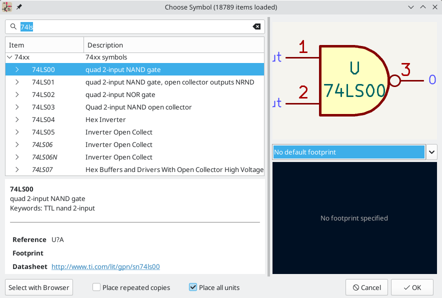
To place a symbol in your schematic, use the ![]() button or the A hotkey. The Choose Symbols dialog appears and lets you select a symbol to add. Symbols are grouped by symbol library.
button or the A hotkey. The Choose Symbols dialog appears and lets you select a symbol to add. Symbols are grouped by symbol library.
By default, only the symbol/library name and description columns are shown. Additional columns can be added by right-clicking the column header and selecting Select Columns.
The Choose Symbol dialog filters symbols by name, keywords, description, and all additional symbol fields according to what you type into the search field.
有一些高级筛选器可用:
-
Wildcards:
*matches any number of any characters, including none, and?matches any single character. -
键值对: 如果一个库部分的描述或关键词包含一个格式为 "Key:123" 的标签,你可以通过输入 "Key>123"(大于)、"Key<123"(小于)等进行相对匹配。数字可以包括以下不区分大小写的后缀之一。
p
n
u
m
k
meg
g
t
10-12
10-9
10-6
10-3
103
106
109
1012
ki
mi
gi
ti
210
220
230
240
-
Regular expressions: if you’re familiar with regular expressions, these can be used too. The regular expression flavor used is the wxWidgets Advanced Regular Expression style, which is similar to Perl regular expressions.
如果符号指定了一个默认的封装,这个封装将在右下方预览。如果符号包括封装过滤器,可以在右边的封装下拉菜单中选择满足封装过滤器的备用封装。
选择一个要放置的符号后,该符号将被附在光标上。 左键点击原理图中所需要的位置,将符号放入原理图中。在将符号放入原理图之前,你可以通过热键或右键菜单来旋转它、镜像它和编辑它的字段。这些操作也可以在放置后进行。
如果 放置重复副本 选项被选中,在放置一个符号后 KiCad 将开始放置该符号的另一个副本。这个过程一直持续到用户按下 Esc。
对于有多个单元的符号,如果 放置所有单元 选项被选中,在放置符号后 KiCad 将开始放置该符号中的下一个单元。 这将持续到最后一个单元被放置或用户按下 Esc。
放置电源符号
一个 《电源符号,电源符号》是一个代表与电源网络连接的符号。 这些符号被分组在 power 库中,所以它们可以使用符号选择器来放置。 然而,由于电源的放置很频繁,![]() 工具是可用的。这个工具也类似,只是搜索是直接在
工具是可用的。这个工具也类似,只是搜索是直接在 power 库和任何其他包含电源符号的库中进行。
移动符号
符号可以用移动(M)或拖动(G)工具移动。这些工具作用于选定的符号,或者如果没有选定符号,则作用于光标下的符号。
移动 工具移动符号本身,而不保持与符号引脚的导线连接。
拖动 工具在移动符号时不会破坏其引脚的导线连接,因此也会移动连接的导线。
你也可以用鼠标点击并拖动符号,这取决于偏好设置中 鼠标和触摸板 部分的 左键拖动手势 设置。
符号也可以旋转(R)或在X(X)或Y(Y)方向上进行镜像。
编辑符号属性
符号的字段可以在符号的属性窗口中进行编辑。用 E 热键或通过双击符号来打开符号属性窗口。
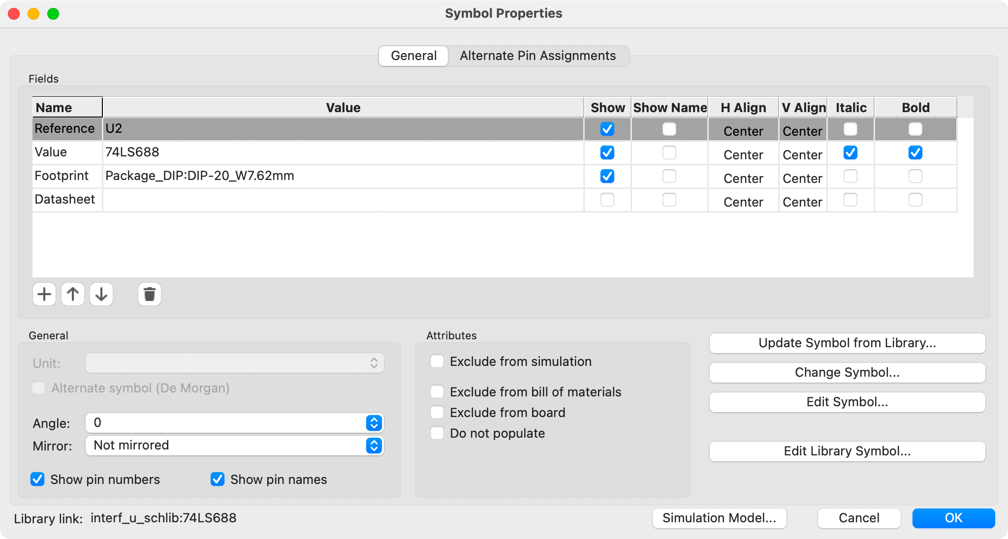
符号属性窗口在一个表格中显示一个符号的所有字段。新的字段可以被添加,现有的字段可以被删除、编辑、重新排序、移动或调整大小。
每个字段的名称和值可以是可见的或隐藏的,并且有几个格式化选项:水平和垂直对齐、方向、位置、字体、文本颜色、文本大小和黑体/大写强调。字段的自动放置也可以在每个字段的基础上启用。对于正常显示的符号,显示的位置总是被指示的(没有旋转或镜像),并且是相对于符号的锚点而言的。
| 符号字段的格式化选项可以通过右击符号字段表的标题行来显示或隐藏,并启用或禁用所需的列。默认情况下,不是所有的列都显示。 |
The Update Symbol from Library… button is used to update the schematic’s copy of the symbol to match the copy in the library. The Change Symbol… button is used to swap the current symbol to a different symbol in the library. These functions are described later.
编辑符号… 打开符号编辑器,编辑原理图中的符号副本。注意,库中的原始符号将不会被修改。编辑库中的符号… 按钮可以打开符号编辑器来编辑库中的原始符号。在这种情况下,原理图中的符号将不会被修改,直到用户点击 更新库中的符号… 按钮。
符号有几个属性,它们会影响 KiCad 其他部分对符号的处理方式。
从模拟中排除 防止该符号被包括在 SPICE 模拟中。
从 BOM 中排除 防止该元件被包括在 《BOM 导出,BOM 导出》中。
从电路板中排除 意味着该符号仅用于原理图,相应的封装不会被添加到 PCB 上。
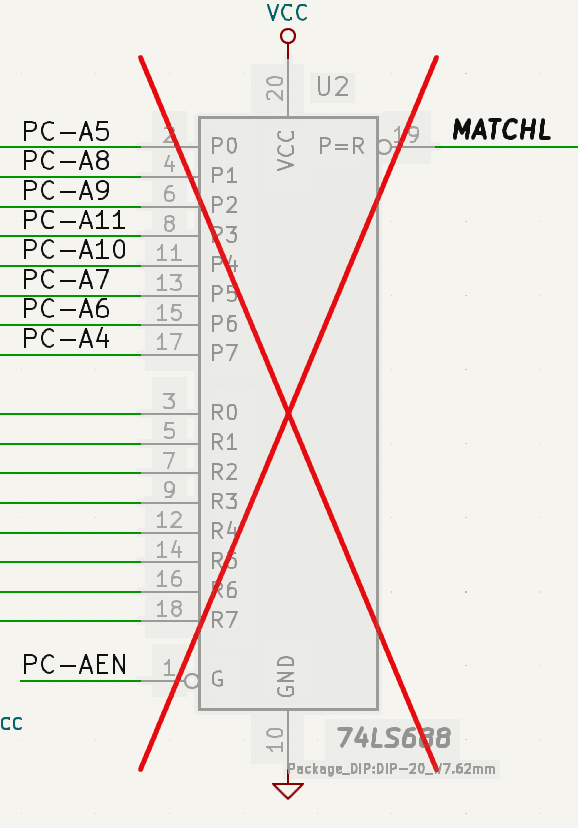
不使用 意味着该元件不应该被连接到 PCB 上,虽然相应的封装仍然应该被添加到电路板上。如下图所示,DNP 符号在原理图中显示为不饱和状态,上面有一个红色的 "X"。
单独编辑符号字段
可以用 E 快捷键直接编辑单个符号文本字段(选择字段而不是符号),或者双击字段。
一些符号字段有自己的快捷键,可以直接编辑它们。选定符号后,可分别用 U、V 或 F 快捷键编辑参考、值和封装字段。
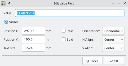
该对话框中的选项与完整的 "符号属性" 对话框中的选项相同,但都是针对单个字段的。
符号字段可以通过自动放置字段操作(选择一个符号并按 O)自动移动到一个适当的位置。字段自动放置可在原理图编辑器的编辑选项中进行配置,包括设置为总是自动放置字段。
Updating and exchanging symbols
When a symbol is added to the schematic, KiCad embeds a copy of the library symbol in the schematic so that the schematic is independent of the system libraries. Symbols that have been added to the schematic are not automatically updated when the library changes. Library symbol changes are manually synced to the schematic so that the schematic does not change unexpectedly.
To update symbols in the schematic to match the corresponding symbol, use Tools → Update Symbols from Library, or right click a symbol and select Update Symbol from Library. You can also access the tool from the symbol properties dialog.
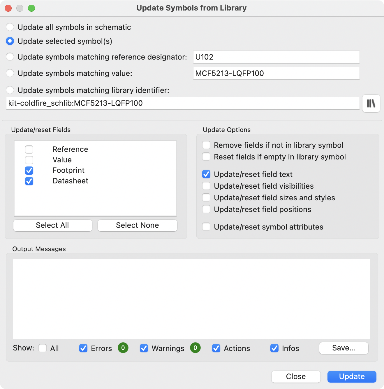
The top of the dialog has options to choose which symbols will be updated. You can update all symbols in the dialog, update only the selected symbols, or update only the symbols that match a specific reference designator, value, or library identifier. The reference designator and value fields support wildcards: * matches any number of any characters, including none, and ? matches any single character.
The middle of the dialog has options to control what parts of the symbol will be updated. You can select specific fields to update or not update, which properties of the fields to update (text, visibility, size and style, and position), and how to handle fields that are missing or empty in the library symbol. You can also choose whether to update symbol attributes, such as do not populate and exclude from simulation / bill of materials / board.
The bottom of the dialog displays messages describing the update actions that have been performed.
To change an existing symbol to a different symbol, use Edit → Change Symbols…, or right click an existing symbol and select Change Symbol…. This dialog is also accessible from the symbol properties dialog.
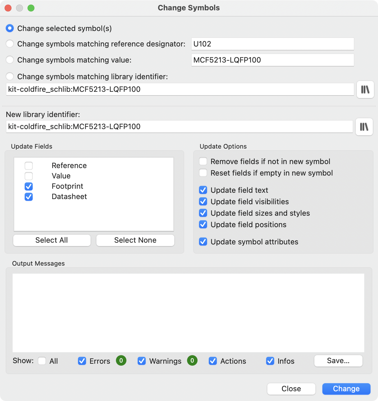
The options for the Change Symbols dialog are very similar to the Update Symbols from Library dialog.
Another way to swap existing symbols for new ones is to use Tools → Edit Symbol Library Links…. This dialog contains a table of every symbol in the design, grouped by current library symbol. By choosing a new symbol in the New Library Reference column, you can make all instances of the existing symbol instead point to the new symbol. If the Update symbol fields from new library option is used, the contents of the existing symbols' fields will be updated to match the new symbols' fields.
The Map Orphans button attempts to automatically remap orphaned symbols to symbols with the same name in an active library. For example, if there is a symbol with the current library reference mylib:symbol123, but the mylib library cannot be found, the Map Orphans button will attempt to find a symbol named symbol123 in any of the libraries that are present. This button is only enabled if orphaned symbols are present in the schematic (see the legacy schematics section).
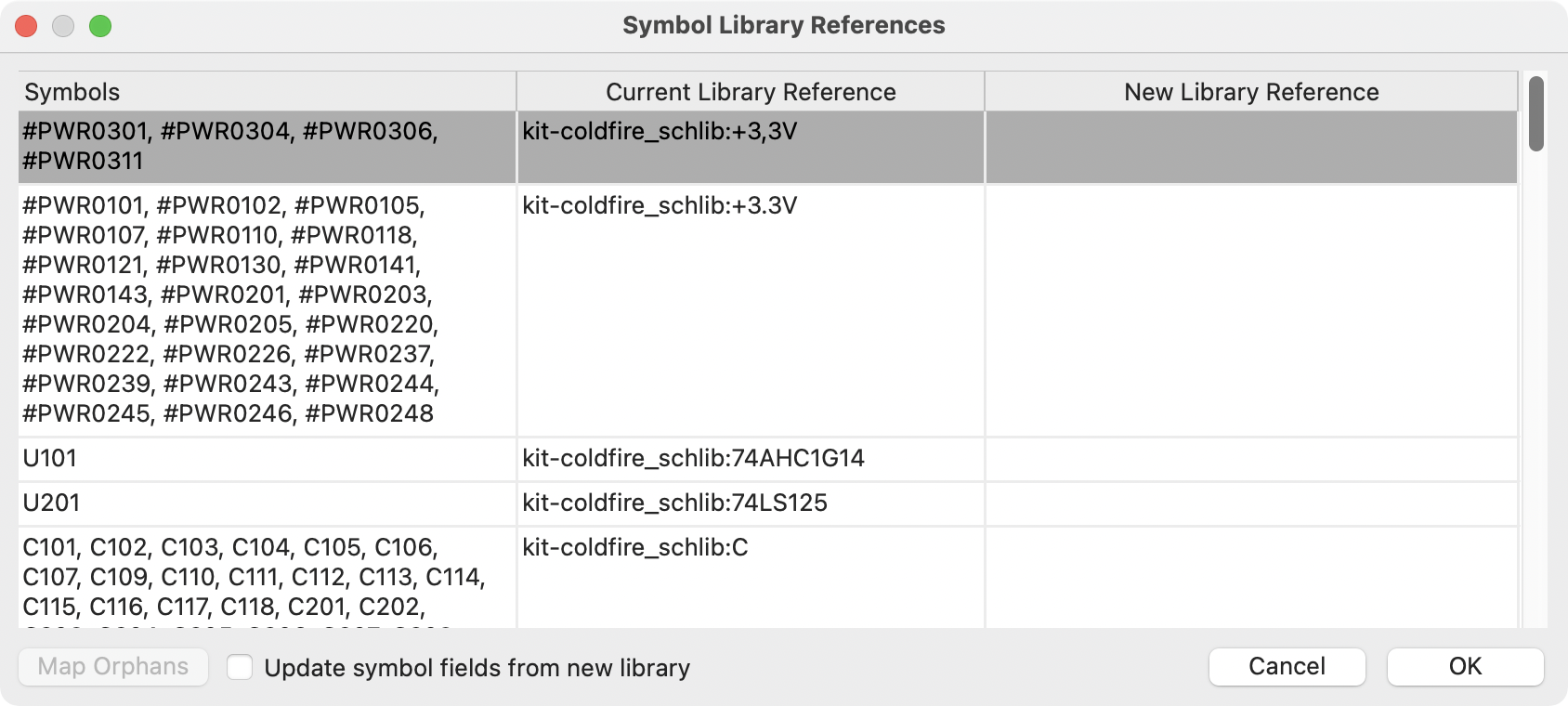
This dialog is primarily useful for managing symbols that appear in multiple libraries, when you want to switch from one library to another. For example, if a schematic uses symbols that are in both a global library and a project-specific library, the Symbol Library References dialog could be used to switch between using the global symbols or the equivalent project-specific symbols. It does not have features for fine-grained control of how fields are updated; for that, use the Change Symbols dialog.
符号字段表
符号字段表允许你在电子表格界面中查看和修改所有符号的字段值。你可以用 ![]() 按钮打开符号字段表。
按钮打开符号字段表。
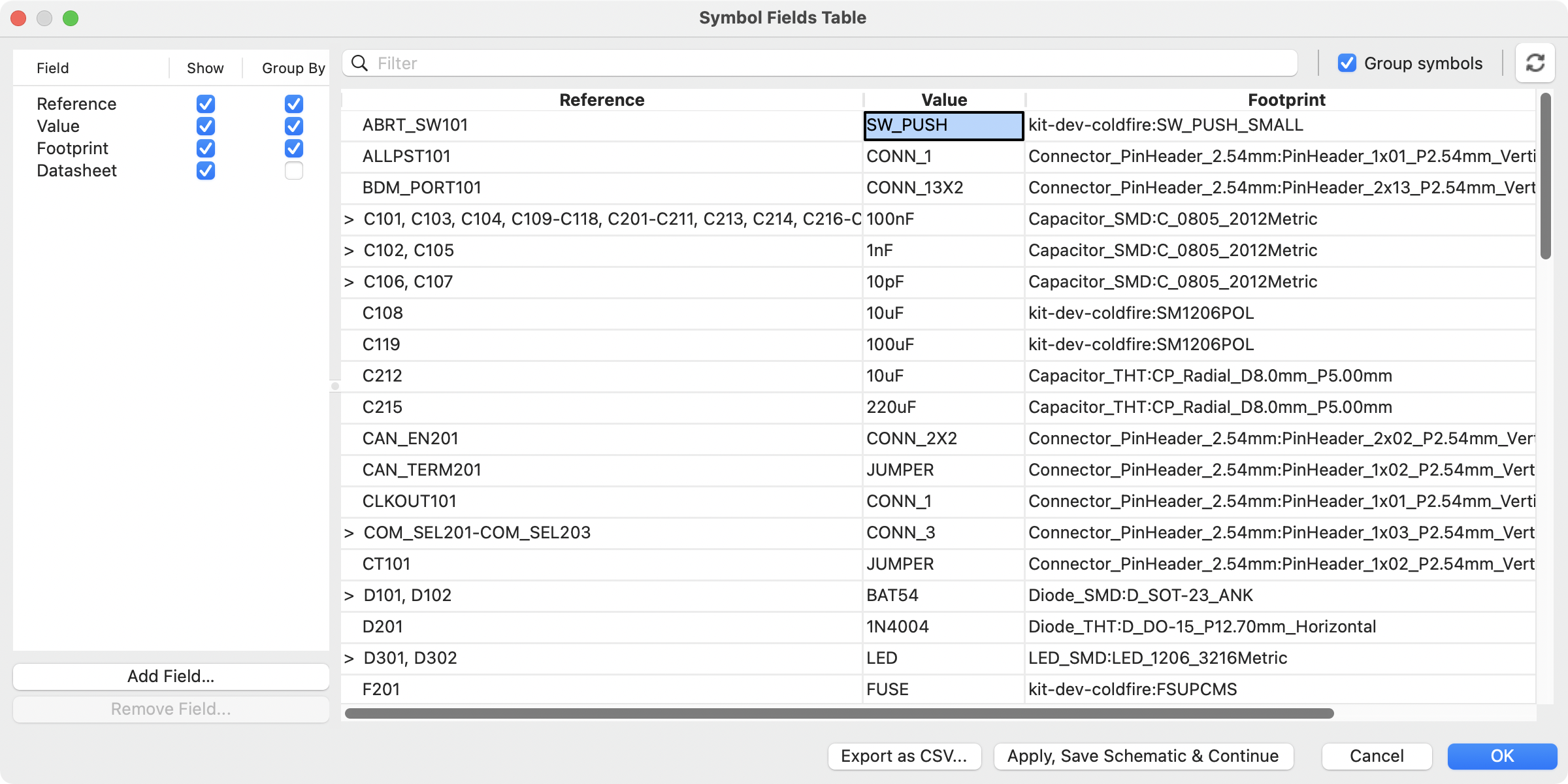
单元格可以用方向键导航,或者用 Tab / Shift+Tab 向右/向左移动,Enter / Shift+Enter 向下/向上移动。
通过点击和拖动可以选择一个单元格范围。选定的整个单元格范围将被复制(Ctrl+C)或粘贴到(Ctrl+V)复制或粘贴操作上。从表中复制单元格的范围对于创建 BOM 非常有用。下面将介绍复制和粘贴单元格的更多细节。
任何符号字段都可以通过左边的 显示 复选框来显示或隐藏,或者通过右键点击表格的标题。新的符号字段可以用 添加字段… 按钮添加。
Similar symbols can optionally be grouped by any symbol field using the Group By checkboxes. Grouped symbols are shown in a single row in the table. The grouped row can be expanded to show the individual symbols by clicking the arrow at the left of the row. The Group Symbols checkbox enables or disables symbol grouping, and the ![]() button recalculates groupings.
button recalculates groupings.
Symbols can be filtered using the Filter textbox at the top. The filter supports wildcards: * matches any number of any characters, including none, and ? matches any single character.
你可以使用 导出为 CSV… 按钮,将符号字段保存到外部文件。这可以作为一个简单的 BOM 生成工具,尽管 《BOM 导出,BOM 工具》提供了对生成的输出的更好控制。
简化填写字段的技巧
电子表格中有几种特殊的复制/粘贴方法,用于将数值粘贴到较大的区域,包括自动增加粘贴的单元格。这些功能在粘贴几个符号中共享的数值时可能很有用。
这些方法如下所示。
| 1. 复制(Ctrl+C) | 2. 选择目标单元格 | 3. 粘贴 (Ctrl+V) |
|---|---|---|
|
|
|
|
|
|
|
|
|
|
|
|
|
|
|
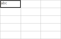
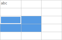
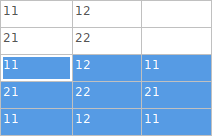
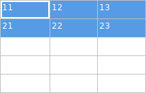
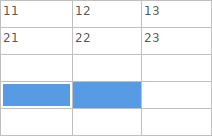
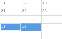
| 这些技术在其他带有网格控制元素的对话框中也可以使用。 |
位号和符号注释
位号是设计中元件的唯一标识符。它们通常被印在 PCB 和装配图上,使你能够将原理图中的符号与电路板上的相应元件相匹配。
在 KiCad 中,位号由一个表示元件类型的字母组成(R 表示电阻,C 表示电容,U 表示集成电路,等等),后面是一个数字。如果符号有多个元位,那么位号也会有一个表示元位的尾部字母。没有设置位号的符号有一个 ? 字符,而不是数字。位号必须是唯一的。
位号可以在符号添加到原理图时自动设置,也可以通过手动编辑单个符号的位号字段或使用注释工具批量设置或重置位号。
| 设置一个符号的位号的过程被称为 批注。 |
自动批注
启用自动批注后,符号被添加到原理图中时将被自动批注。你可以在 偏好设置 中 原理图编辑器 → 批注选项 窗格中选中 自动批注符号 复选框来启用自动批注。自动批注也可以通过左侧工具栏的 ![]() 按钮进行切换。
按钮进行切换。
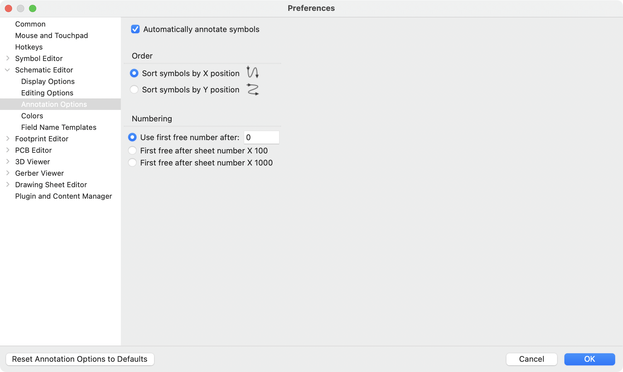
当同时添加多个符号时,它们会根据 顺序 设置进行批注,按 X 或 Y 位置排序。
编号 选项为新的位号设置起始编号。 这可以是最低的可用数字,也可以是基于原理图编号的数字。
关于注解选项的更多信息,请参见《批注工具,批注工具》的文档。
批注工具
批注工具会自动为原理图中的符号指定位号。要启动批注工具,请点击顶部工具栏上的 ![]() 按钮。
按钮。
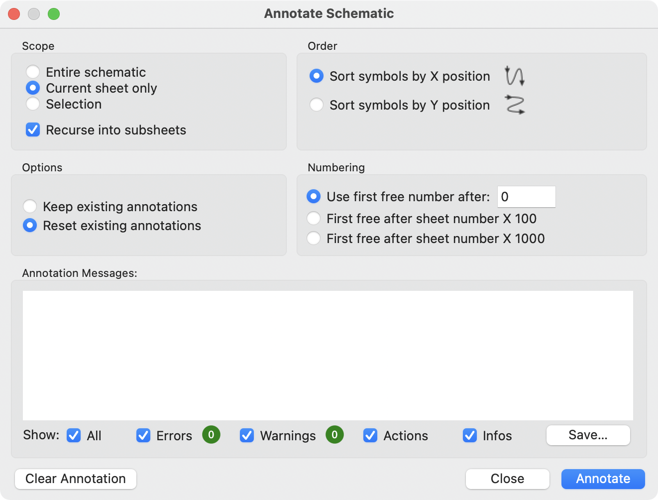
该工具提供了几个选项来控制符号的批注方式。
范围: 选择批注是否适用于整个原理图、仅适用于当前原理图或仅适用于选定的符号。如果选择了 递归到子原理图 的选项,所选范围的子原理图中的符号将被重新批注;否则子原理图中的符号将不会被重新批注。例如,如果 递归到子原理图 和 仅选择,任何选定的子原理图中的符号将被重新批注。
选项: 选择批注是否应适用于所有符号和重置 现有的位号,或仅适用于未批注的符号。
顺序: 选择编号的方向。如果符号按 X 位置排序,原理图页面左侧的所有符号将比页面右侧的符号编号低。如果符号按 Y 位置排序,则原理图顶部的所有符号的编号将低于原理图底部的符号的编号。
编号: 选择编号位号的起点。每一个位号都会选择在起点之上的最低的未使用的数字。起始点可以是一个任意的数字(通常是 0),也可以是纸张编号乘以 100 或 1000,这样每个零件的位号就与它所在的原理图页相对应。
清除批注 按钮可以清除所选范围内的所有位号。
批注信息可以用底部的复选框进行过滤,或用 保存… 按钮保存到报告中。
电气连接
有两种主要的方式来建立连接:导线和标签。导线进行直接连接,而标签则与具有相同名称的其他标签连接。下面的原理图中显示了导线和标签的情况。
也可以用总线进行连接,并通过隐藏的电源引脚进行隐性连接。
本节还将讨论两种特殊类型的符号,可以用右侧工具栏上的 "电源符号" 按钮添加:
-
电源符号:用于将电线连接到电源或地网络的符号。
-
PWR_FLAG:一个特定的符号,用于表示一个网络在没有连接到电源输出引脚时是有电源的(例如,一个由板外连接器提供的电源网络)。
导线
导线用于在两点之间直接建立电气连接。 要建立连接,必须将一段导线的末端与另一段导线或一个引脚相连。只有导线的末端才能建立连接;如果一根导线穿过另一根导线的中间,就不会建立连接。
未连接的导线端有一个小方块,表示连接点。 当连接到导线端时,这个方块就会消失。未连接的引脚有一个圆圈,当进行连接时也会消失。
| 导线只有在两端完全重合的情况下才能与其他导线或引脚连接。因此,保持符号引脚和导线与网格对齐很重要。建议在放置符号和绘制导线时始终使用 50 mil 的网格,因为 KiCad 标准符号库和所有遵循其风格的库也使用 50 mil 的网格。 |
| 符号、导线和其他没有对准网格的元素,可以通过选择它们,右键点击,并选择 将元素对准网格,来将它们重新对准网格。 |
绘制和编辑电线
要开始用导线连接元素,请使用右侧工具栏中的导线工具 ![]() (w)。也可以通过点击未连接的符号引脚或导线末端来自动启动导线。
(w)。也可以通过点击未连接的符号引脚或导线末端来自动启动导线。
你可以用左边工具栏上的 ![]() 按钮将导线限制在 90 度角,或者用
按钮将导线限制在 90 度角,或者用 ![]() 按钮限制在 45 度角。
按钮限制在 45 度角。![]() 按钮允许你以任何角度放置导线。你可以使用 Shift+Space 在这些模式中循环,或者在 偏好设置 → 原理图编辑器 → 编辑选项 中选择所需的模式。这些模式除了影响导线外,还影响 《图形线,图形线》。
按钮允许你以任何角度放置导线。你可以使用 Shift+Space 在这些模式中循环,或者在 偏好设置 → 原理图编辑器 → 编辑选项 中选择所需的模式。这些模式除了影响导线外,还影响 《图形线,图形线》。
As in the PCB editor, the / hotkey switches wire posture.
可以使用移动(M)或拖动(G)工具来移动和编辑导线。 与符号一样,移动 工具只移动选定的线段,而不保持与其他线段的现有连接。而 拖动 工具则保持现有的连接。
你可以使用 选择连接 工具(Alt+4)选择连接的导线。这个工具可以选择所有连接的线段,直到到达一个结点,从所选线段或光标下的线段开始。 再次使用该工具可以将现有的选择范围扩大到下一个结点。
你可以通过右击导线并选择 切片 将一个线段分成两块。该线段将在当前的鼠标位置被分开。你也可以通过右击一个线段并选择 断开 将其与相邻的线段分开。
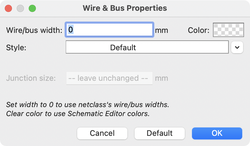
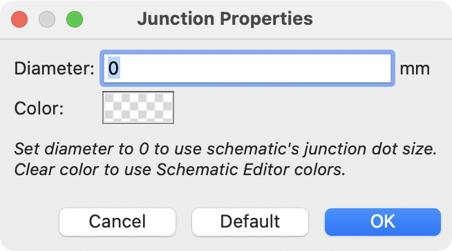
通常情况下,线的线型是按照网的《原理图设置网络类,网络类设置》(如果没有指定其他网络类,网就处于 默认 网络类)。然而,所选线段的线型可以在线段的属性对话框中被覆盖(当线段被选中时 E)。可以设置线的宽度、颜色和线的样式(实线、虚线、点线等)。将宽度设置为 0,清除颜色,并使用 默认 线条样式,分别使用网络类设置中的默认宽度、颜色和样式。如果在选择中包含了一个导线结点,结点的大小也可以在这里进行编辑。
导线结点
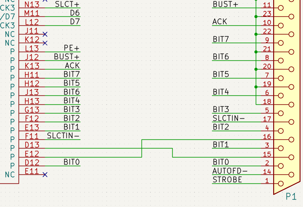
交叉的导线不会被隐含地连接起来。如果需要连接,有必要通过明确地添加结点来连接它们(![]() 按钮在右侧工具栏)。交叉点将被自动添加到开始或结束于现有导线之上的导线。
按钮在右侧工具栏)。交叉点将被自动添加到开始或结束于现有导线之上的导线。
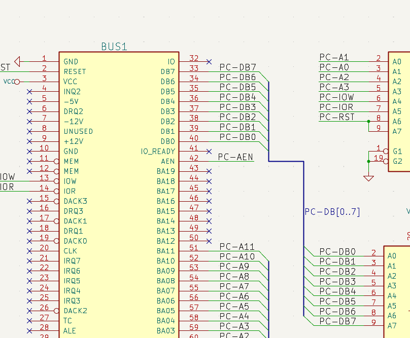
在上面的原理图中,连接到 P1 引脚 18、19、20、21、22 和 23 的导线上使用了结点。
结点大小自动遵循原理图的 结点大小 设置,在 原理图设置 → 通用 → 格式化。颜色遵循 《原理图设置网络类,网络类设置》。自动尺寸和颜色可以在每个连接点的属性中被覆盖;尺寸为 0 相当于原理图的默认尺寸,而清除颜色则使用网络类颜色。
标签
标签是用来给导线和引脚分配网络名称的。具有相同网络名称的导线被认为是连接在一起的,所以标签可以用来进行连接,而不需要直接画线连接。
一个网络只能有一个名称。如果有两个不同的标签放在同一个网络上,将产生一个 ERC 违规。 在网表中只使用其中一个网络名称。最终的网络名称是根据下面描述的《网络名称分配规则》决定的。
有三种类型的标签,每种都有不同的连接范围。
-
局部标签,也被简单地称为标签,只在一个原理图内进行连接。用右边工具栏上的
 按钮添加一个局部标签。
 -
全局标签 可以在原理图的任何地方进行连接,而不考虑原理图。用右边工具栏上的
 按钮添加一个全局标签。
 -
层次标签 连接到层次的原理图页码,在《层次原理图,层次原理图》中用于连接子原理图和其父原理图。用右边工具栏上的
 按钮添加层次标签。
| 具有相同名称的标签将被连接,无论标签类型如何。如果它们在同一张原理图上。 |
添加和编辑标签
使用适当的按钮或快捷键创建标签后,会出现标签属性对话框。
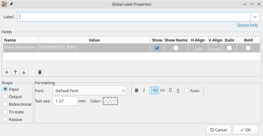
标签 字段设置了标签的文本,它决定了标签分配给其连接线的网络。标签文本支持《文本标记,标记》,用于覆盖条、下标等,以及《文本变量,变量替换》。 使用对话框中的 语法帮助 链接来获得摘要。
有几个选项可以控制标签的外观。你可以改变文本的 《字体,字体》、大小和颜色,并设置粗体和斜体强调。 你还可以设置文本相对于标签连接点的方向。层次和全局标签有几个额外的选项:自动 选项根据连接的原理图元素自动设置标签方向,形状 选项控制标签轮廓的形状(输入、输出、双向、三态 或 被动)。轮廓形状纯粹是视觉上的,没有电气上的影响。
| The default text size can be set for a schematic in Schematic Setup, and the default font can be set in Preferences. |
| Global labels have additional settings to control margins around the label text in the Schematic Setup dialog. |
标签也可以添加字段。有两个字段有特殊的意义("网络类" 和 "位表间参考",下面会介绍),但也可以添加任意字段。标签字段的行为类似于《编辑符号属性,符号字段》:你可以显示或隐藏它们的名称和值,调整对齐方式、方向、位置、大小、字体、颜色和强调。
| 通过右击标签字段表的标题行,启用或禁用所需的列,可以显示或隐藏标签字段的格式化选项。默认情况下,不是所有的列都显示。 |
与符号字段一样,标签字段可以通过从原理图中打开特定标签字段的属性进行单独编辑(双击标签字段,或使用 E)。
接受标签属性后,标签将被连接到光标上进行放置。标签的连接点是标签角落里的小方块。当标签被连接到导线或引脚的末端时,这个方块就会消失。

连接点相对于标签文本的位置可以通过在标签的属性中选择不同的标签方向,或通过镜像/旋转标签来改变。
通过选择一个标签并使用 E 快捷键、双击该标签或在右键菜单中使用 属性…,可以随时访问标签属性对话框。
用标签分配网络类
In addition to assigning net names, labels can be used to assign net classes. A label field named Net Class assigns the specified netclass to the net associated with the label. To make it easier to assign net classes in this way, Net Class is the default name for new label fields, and Net Class fields present a dropdown list of all the net classes in the design. Net classes must be created in the Schematic Setup or Board Setup windows before they can be assigned with a label field.
关于分配网络类的更多信息,请参见《原理图网络类,网络类文档》。
表间参考
全局标签可以显示表间参考,这是原理图中出现同一全局标签的其他地方的页码列表。 点击表间参考就可以进入所列出的页面。如果列出了多个位号,点击位号列表会出现一个菜单来选择所需的页面。
Inter-sheet references are globally controlled in the Schematic Setup window’s Formatting page. References can be enabled or disabled, and the displayed format for the list can be adjusted, including with optional prefix or suffix characters.
下图显示了一个全局标签,其中有对其他两个原理图页面的之间位号。在原理图设置中,分别添加了前缀和后缀 [ 和 ]。
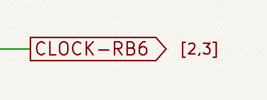
全局标签会自动添加一个 "表间参考" 字段,其值为 "${INTERSHEET_REFS}",用于控制该标签的表间参考。${INTERSHEET_REFS} 文本变量会被扩展为全局标签的表间参考的完整列表,如在原理图设置中所配置。表间参考的可见性在 "原理图设置" 中是全局控制的,而不是通过 "表间参考" 字段的可见性控制。对于其他类型的标签,"表间参考" 字段没有意义。
总线
总线是一种在原理图中分组相关信号的方法,以简化复杂的设计。 总线可以像导线一样用总线工具画出来 ![]() ,并像信号线一样用标签命名。
,并像信号线一样用标签命名。
在下面的原理图中,许多引脚都连接到总线上,也就是中间的蓝色粗线。
总线编号
在 KiCad 6.0 及以后版本中,有两种类型的总线:矢量总线和分组总线。
一个 矢量总线 是一个信号的集合,以一个共同的前缀开始,以一个数字结束。 矢量总线被命名为 <前缀>[M..N],其中`前缀`是任何有效的信号名称,M 是第一个后缀数字,N 是最后的后缀数字。 例如,总线 DATA[0…7] 包含信号 DATA0、DATA1,以此类推,直到 DATA7。 指定 M 和 N 的顺序并不重要,但两者必须是非负数。
一个 分组总线 是一个或多个信号和/或矢量总线的集合。 分组总线可以用来把相关的信号捆绑在一起,即使它们有不同的名字。 分组总线使用一种特殊的标签语法:
<OPTIONAL_NAME>{SIGNAL1 SIGNAL2 SIGNAL3}
该分组的成员被列在大括号({})内,用空格字符隔开。 在大括号的前面有一个可选的分组名。 如果分组总线没有命名,PCB 上的结果网络将只是该分组内的信号名称。 如果分组总线有名字,产生的网路将以名字为前缀,用句号(.)分隔前缀和信号名称。
例如,总线 {SCL SDA} 有两个信号成员,在网表中这些信号将是 SCL 和 SDA。 总线 USB1{DP DM} 将产生名为 USB1.DP 和 USB1.DM 的网表。 对于在几个类似电路中重复出现的较大的总线的设计,使用这种技术可以节省时间。
分组总线也可以包含矢量总线。 例如,总线 MEMORY{A[7..0] D[7..0] OE WE} 同时包含了矢量总线和普通信号,并将在 PCB 上形成 MEMORY.A7 和 MEMORY.OE 这样的网络。
总线的绘制和连接方式与信号线相同,包括使用结点来创建交叉线之间的连接。 与信号线一样,总线不能有一个以上的名称—如果在同一条总线上有两个冲突的标签,将产生一个 ERC 违规。
总线成员之间的连接
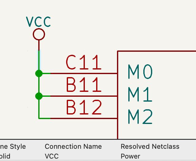
在总线的相同成员之间连接的引脚必须通过标签连接。不可能将一个引脚直接连接到总线上;这种连接方式将被 KiCad 忽略。
在上面的例子中,连接是通过放置在连接到引脚的导线上的标签来实现的。通往总线的总线入口(45 度的线段)只是图形化的,并不是形成逻辑连接的必要条件。
事实上,使用重复命令(Insert),如果元件引脚以递增的顺序排列,可以非常快速地进行连接(在实践中,这种情况常见于存储器、微处理器等元件):
-
放置第一个标签(例如:
PCA0)。 -
根据需要使用重复命令来放置成员。 KiCad 将自动创建下一个标签(
PCA1,PCA2…)垂直对齐,理论上是在其他引脚的位置上。 -
在第一个标签下画线。然后使用重复命令将其他导线放在标签下。
-
如果需要,以同样的方式放置总线入口(放置第一个入口,然后使用重复命令)。
|
在偏好设置菜单的 原理图编辑器 → 编辑选项 部分,你可以设置重复的参数:
|
总线展开
展开工具允许你快速地从总线上分离出信号。 要展开一个信号,请右击一个总线对象(一个总线导线等),并选择 从总线上展开。 或者,当光标在一个总线对象上时,使用 展开总线 快捷键(默认:C)。 该菜单允许你选择要展开的总线成员。
在选择总线成员后,下一次点击将把总线成员的标签放在所需的位置。 该工具会自动生成一个总线入口和通向标签位置的导线。 放置完标签后,你可以继续放置额外的线段(例如,连接到一个元件引脚),并以任何正常方式完成布线。
总线别名
总线别名是一种快捷方式,可以让你更有效地处理大型组总线。 它们允许你定义一个组总线,并给它一个简短的名称,然后可以在整个原理图中代替完整的组名称。
要创建总线别名,请在《原理图设置,原理图设置》中打开 总线别名定义 窗格。
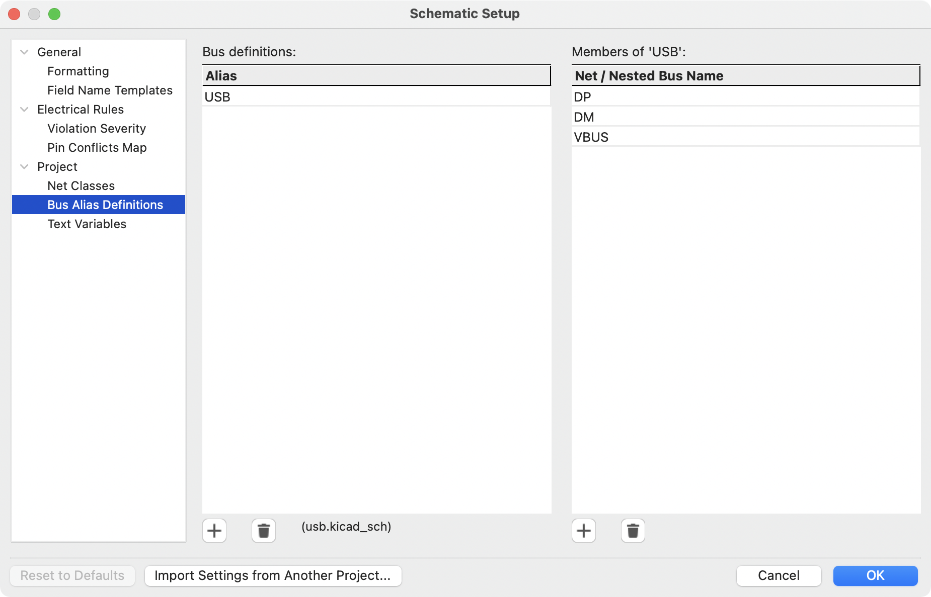
一个别名可以被命名为任何有效的信号名称。 使用该对话框,你可以向别名添加信号或矢量总线。 作为一种快捷方式,你可以输入或粘贴信号和/或总线的列表,用空格隔开,它们将全部被添加到别名定义中。 在这个例子中,我们定义了一个名为 USB 的别名,成员为 DP、DM 和 VBUS。
定义别名后,可以在组总线标签中使用,方法是将别名放在分组总线的大括号内:{USB}。 这与给总线贴上`{DP DM VBUS}` 标签的效果相同。 你也可以给分组添加一个前缀名,比如 USB1{USB},这样就会产生如上面所说的 USB1.DP 这样的网路。 对于复杂的总线,使用别名可以使原理图上的标签短得多。 请记住,别名只是一个快捷方式,别名的名称不包括在网表中。
总线别名被保存在创建别名时打开的原理图文件中。在 总线别名定义 窗口中,与所选别名相关的原理图文件显示在别名列表的底部。在一个给定的原理图工作表中创建的任何别名都可以在同一层次设计中的任何其他原理图工作表中使用。如果一个层次设计中的多个原理图包含相同名称的总线别名,这些别名必须都有相同的成员。如果多个同名的总线别名没有一致的成员,《ERC 检查列表,ERC 将报告违规情况》。
有多个标签的总线
KiCad 5.0 和更早的版本允许将具有不同标签的总线连接在一起,并在网表编制时将这些总线的成员连接起来。这种行为在 KiCad 6.0 中被删除了,因为它与分组总线不兼容,而且还会导致网表的混乱,因为一个给定的信号将得到的名称不容易预测。
如果您在现代版本的 KiCad 中打开使用此功能的设计,您将看到“迁移总线”对话框,该对话框将指导您更新原理图,以便在任何给定的总线线路上只存在一个标签。
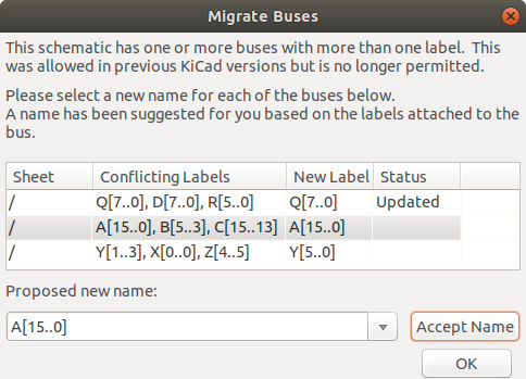
对于具有多个标签的每组总线,您必须选择要保留的标签。 下拉名称框允许您在设计中存在的标签之间进行选择,或者您可以通过手动将其输入新名称字段来选择其他名称。
隐藏电源引脚
当一个符号的电源引脚是可见的,它们必须被连接,就像其他信号一样。然而,诸如门和触发器等符号有时会画出隐含的电源输入引脚,这些引脚是隐性连接的。
KiCad 会自动将类型为 "电源输入" 的隐形引脚连接到与该引脚同名的全局网络。例如,如果一个符号有一个名为 VCC 的隐藏电源输入引脚,这个引脚将被全局连接到所有原理图上的 VCC 网络。
|
隐藏的引脚可以在原理图中显示,方法是在 原理图编辑器 → 偏好设置的 显示选项 部分勾选 显示隐藏的引脚,或者选择 视图 → 显示隐藏的引脚。在左边的工具栏上还有一个切换图标 |
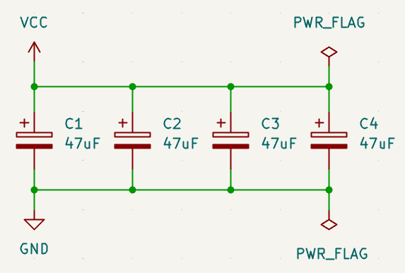
可能有必要将不同名称的电源网络连接起来(例如,TTL 元件中的 GND 和 MOS 元件中的 VSS)。为了达到这个目的,为每个网络添加一个 《电源符号,电源符号》,并用一根导线连接它们。
如果使用隐藏的电源引脚,不建议使用本地标签进行电源连接,因为它们不会连接到其他片上的隐藏电源引脚。
| 对隐藏的电源输入引脚必须小心,因为它们可能会产生无意的连接。从本质上讲,隐藏的引脚是不可见的,不显示其引脚名称。这使得很容易意外地将两个电源引脚连接到同一个网络。由于这个原因,不建议 在电源符号之外 使用隐形电源引脚,只支持与传统设计和符号兼容。 |
电源符号
电源符号是传统上用来表示与电源网连接的符号,如`VCC` 或 GND。除了作为连接网络是电源布线的视觉指示外,电源符号还可以进行全局连接:两个具有相同引脚名称的电源符号在原理图中的任何地方都可以相互连接,而不用考虑原理图。
Power symbols are virtual: they do not represent a physical component on the PCB.
在下图中,电源符号用于将电容器的正负极分别连接到 VCC 和 GND 网路上。
In the KiCad standard library, power symbols are found in the power library, but power symbols can be created in any library.
To create a custom power symbol, make a new symbol with a power input pin that is set to be invisible. Name the pin according to the desired power net. In addition, set the "Define as power symbol" symbol property. As described in the hidden power pins section, invisible power input pins make global connections based on the hidden power pin’s name. The process of creating a power symbol is described in more detail in the Symbol Editor section.
| 连接的网名是由电源符号的 引脚名称 决定的,而不是符号的名称或值。这意味着电源符号的网名只能在符号编辑器中改变,不能在原理图中改变。 |
网络名分配规则
原理图中的每个网都被分配了一个名称,无论这个名称是由用户指定还是由 KiCad 自动生成。
当多个标签附加到同一个网时,最终的网络名将按以下顺序确定,从最高优先级到最低:
-
全局标签
-
《电源符号,电源符号》
-
局部标签
-
层次标签
-
测试原理图页码
如果一个网络有多个同一类型的标签,则按字母顺序排序,使用第一个。
如果一个网络穿过《层次原理图,层次》的多张原理图,它将从它有层次标签或局部标签的层次结构的最高层取名。通常,局部标签优先于层次标签。
如果上面的标签类型都没有附加到网络中,那么网络的名称将根据连接的符号引脚自动生成。
PWR_FLAG
在上面的截图中可以看到两个 PWR_FLAG 符号。它们向 ERC 表明,两个电源网络 VCC 和 GND 实际上连接到一个电源上,因为没有明确的电源,如连接到任何一个网络的电压调节器输出。
如果没有这两个标志,ERC 工具会诊断出:错误:输入电源引脚没有被任何输出电源引脚驱动。
PWR_FLAG 符号可以在 power 符号库中找到。通过将任何电源输出引脚连接到网络上,可以达到同样的效果。
无连接标志
No-connection flags (![]() ) are used to indicate that a pin is intentionally unconnected. These flags prevent "unconnected pin" ERC warnings for pins that are intentionally unconnected.
) are used to indicate that a pin is intentionally unconnected. These flags prevent "unconnected pin" ERC warnings for pins that are intentionally unconnected.
Note that no-connection flags are distinct from the "unconnected" symbol pin type, although they both prevent "unconnected pin" ERC warnings on the pin in question.
网络类
网络类是可以被分配设计规则(用于 PCB)和图形属性(用于原理图)的网络类。在 KiCad 中,每个网络都是一个网络类的一部分。如果你不把一个网络添加到一个特定的类中,它将是默认类的一部分,它总是存在。
网络类可以在原理图或电路板设置对话框中创建和编辑。可以使用下面描述的基于模式的分配将网络添加到原理图或电路板的网络类中。网络也可以用网络类指令或《标签网络类,网络标签》的图形分配到原理图中的网络类。
选择一个导线或标签会在窗口底部的信息面板中显示该网络的网络类。
在原理图设置中管理网络类
网络类在 原理图设置 对话框的 网络类 面板中管理。
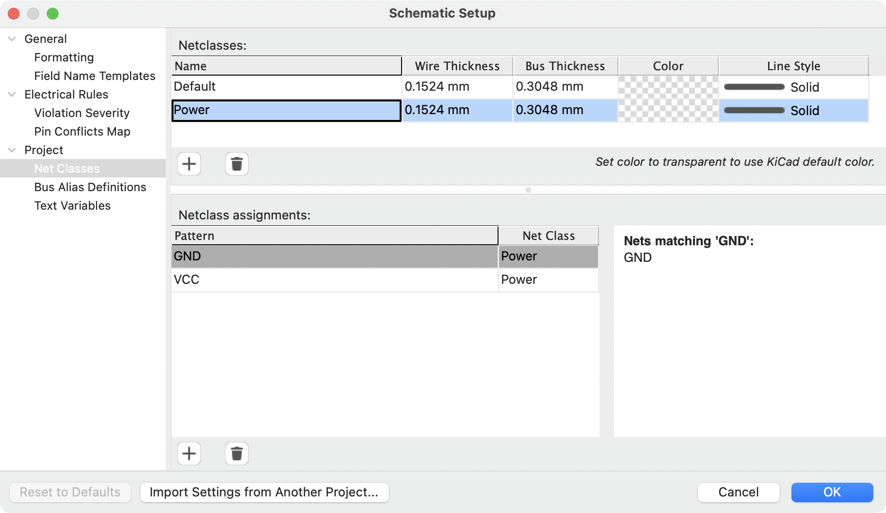
顶部的窗格列出了设计中存在的网络类。默认 网络类总是存在的,你可以通过 ![]() 按钮添加额外的网络类,或者通过
按钮添加额外的网络类,或者通过 ![]() 按钮删除选定的网络类。
按钮删除选定的网络类。
每个网络类可以有独特的图形属性,决定该网络类的导线如何在原理图中显示。导线和母线的厚度、颜色和线条风格(实线、虚线、点线等)都可以调整。将颜色设置为透明将使用主题的默认导线/总线颜色,该颜色可在《偏好设置颜色,偏好设置》中配置。
You can also set board design rules for each netclass, although the DRC fields are hidden by default. Right click the header row to show or hide additional columns. For more information about setting netclass design rules, see the PCB editor documentation.
The bottom pane lists pattern-based netclass assignments. Each row has a net name pattern and a netclass; nets with names that match the pattern are assigned to the specified netclass. If a net matches multiple patterns, the first match is used. Pattern-based netclass assignments are dynamic: when a new net is added that matches an existing pattern, it will be assigned to the associated netclass automatically. Net patterns can use both wildcards (* to match any number of any characters, including none, and ? to match any character) and regular expressions. The nets that match the selected pattern are displayed to the right of the pattern list.
For example, the net* pattern matches nets named net, net1, network, and any other net name beginning with net. Because * has a slightly different meaning in a regular expression (* matches zero or more of the preceding character), the net* pattern would also match a net named ne.
记住,网络名必须包括完整的工作表路径。例如,一个 在根原理图中的本地标记的网有一个以 / 为前缀的名称。
|
使用 ![]() 按钮来添加网络类分配模式,或
按钮来添加网络类分配模式,或 ![]() 按钮来删除模式。
按钮来删除模式。
A netclass pattern containing only the * wildcard will match all
explicitly named nets, but will not match unlabeled nets. To match
unlabeled nets, you can include more of the net name before the wildcard
character. All unlabeled nets have names that begin with Net-, so the
pattern Net-* will match all unlabeled nets. You can also assign a
netclass to an unlabeled net using a
net class directive.
|
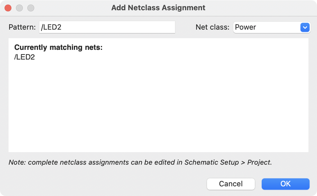
您可以从原理图画布上直接创建网络类图案,而不是在原理图设置对话框中添加网络类图案。右击一个网络,选择分配网络类…,就会出现添加网络类分配对话框。网络类模式会预先填上所选网络的名称,但如果需要,也可以改变模式。所有符合该模式的网都显示在对话框中。
在原理图中以图形方式分配网络类
作为基于模式的网络类分配的替代方法,网络类可以用 网络类指令 或 标签 以图形方式分配给原理图中的网络。网络类必须在《原理图设置网络类,原理图设置》中创建,然后才能以图形方式分配。
在下面的图片中,一个网络类指令被用来给 50R 网络类分配信号。
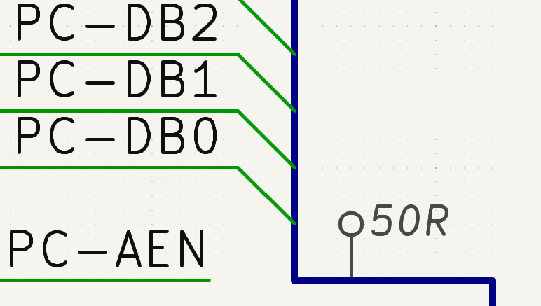
网络类指令是通过右边工具栏的 ![]() 按钮添加的。它们的行为类似于《标签,标签》,除了它们不能被用来命名一个网络。根据指令的
按钮添加的。它们的行为类似于《标签,标签》,除了它们不能被用来命名一个网络。根据指令的 网络类 字段的值,附加的网络被分配了一个网络类。`网络类`字段提供了一个设计中所有网络类的下拉列表。
如果一个指令被附加到一个总线上,总线上的所有成员都被分配到指定的网络类。
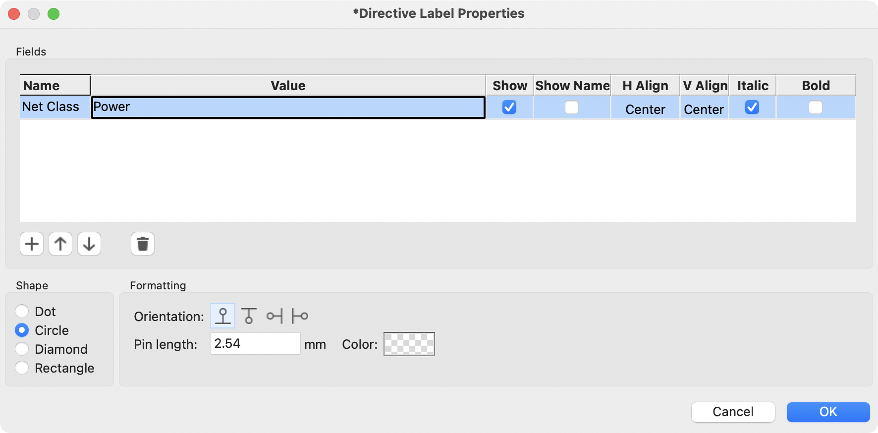
除了相关的网络类,你还可以在指令的属性中编辑指令的形状(点、圆、钻石或矩形)、方向、引脚长度 和 颜色。
《标签网络类,网络标签也可以用来给网络分配网络类》,方法是在标签中添加一个 网络类 字段。
如果超过一个不同的网络类被图形化地分配给一个网络,《ERC 检查清单,ERC 将报告一个问题》。图形化的网络类分配优先于基于模式的分配:如果一个网络与网络类模式分配相匹配,并且也有一个图形化的网络类分配,那么将使用图形化的网络类分配。
图形项目
文字、图形和图像可以被添加到原理图中,用于记录。这些项目对原理图没有任何电气影响。
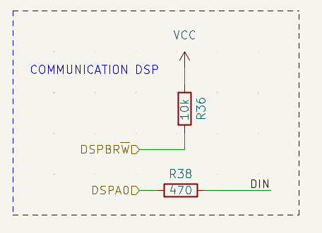
下面的图片除了符号和几种类型的标签外,还显示了图形线和文字("COMMUNICATION DSP")。
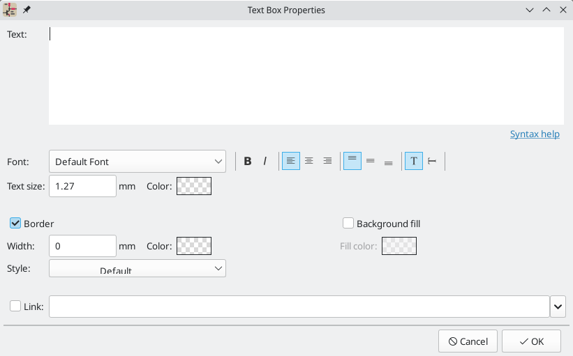
文本和文本框
有两种文本可以被添加到原理图中,它们被称为文本(![]() )和文本框(
)和文本框(![]() )。两者都是使用右侧工具栏中各自的按钮添加的。
)。两者都是使用右侧工具栏中各自的按钮添加的。
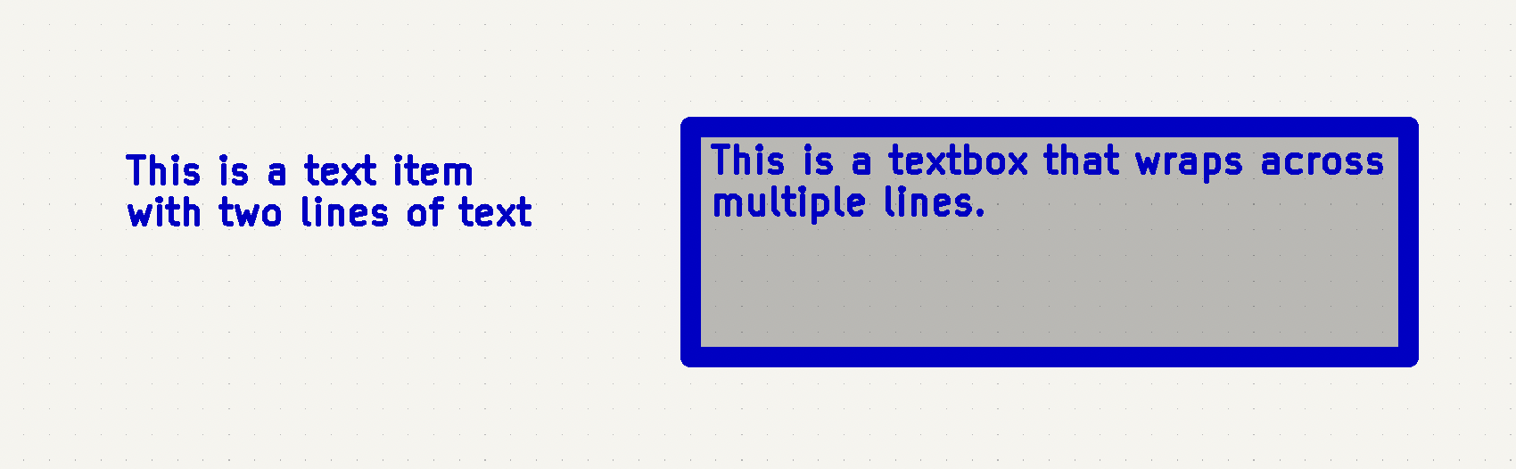
这两种文本项目都支持多行文本和基本的格式化功能,但文本框将文本包起来以适应大纲,并有额外的格式化选项。所有的文本都有可调整的字体、颜色、大小、黑体和斜体强调,左右对齐,以及垂直和水平方向。文本框还支持水平居中,垂直对齐选项,以及彩色边框和填充。
| The default text size can be set for a schematic in Schematic Setup, and the default font can be set in Preferences. |
链接
文本和文本框可以通过在文本属性的 链接 框中输入一个目标而成为一个链接。链接目标可以是一个本地文件(使用 file:// 协议前缀,后跟文件路径),到一个网站(使用 http:// 或 https://,后跟其余的 URL),或到同一图示中的另一个页面(使用 # 后跟页码)。这些也可以使用链接目标框中的下拉菜单自动填写。
字体
文本和文本框支持自定义字体,可通过文本的属性对话框中的 字体 下拉选择。除了 KiCad 字体外,你还可以使用安装在你电脑上的任何 TTF 字体。
| 用户字体不会被嵌入工程中。如果该工程在另一台没有安装所选字体的计算机上打开,将会有不同的字体被替换。为了获得最大的兼容性,请使用 KiCad 字体。 |
文本标记
Text supports markup for superscripts, subscripts, overbars, evaluating project variables, and accessing symbol field values.
| Feature | Markup Syntax | Result |
|---|---|---|
Superscript |
|
textsuperscript |
Subscript |
|
textsubscript |
Overbar |
|
text |
|
variable_value |
|
|
field_value of symbol refdes |
| Variables must be defined in Schematic Setup before they can be used. There are also a number of built-in system text variables. |
图形形状
图形矩形(![]() )、圆形(
)、圆形(![]() )、弧形(
)、弧形(![]() )和直线(
)和直线(![]() )都可以使用右侧工具栏中各自的按钮添加。
)都可以使用右侧工具栏中各自的按钮添加。

线条的宽度、颜色和样式(实线、虚线或点线)可以在每个形状(E)的属性对话框中进行配置。矩形、圆形和弧线也可以设置填充颜色并去除其轮廓。
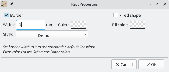
Setting a shape’s line width to 0 uses the schematic default line width, which is configurable in Schematic Setup. Spacing for line dashes is also configurable there. Removing a line or fill color uses the color theme’s graphics color, which is configurable in Preferences.
像《画和编辑导线,导线》一样,图形线服从线的绘制模式设置(90 度,45 度,或自由角度),你可以用左边工具栏上的切换按钮来设置(,
![]() ,和
,和 ![]() ,分别)。 Shift+Space 循环浏览这些模式。
,分别)。 Shift+Space 循环浏览这些模式。
As with PCB tracks, the / hotkey switches line posture.
位图图像
位图图像可以通过 ![]() 按钮添加到原理图中。原理图中的图像可以被移动和缩放。属性对话框允许设置位置和比例,以及将图像转换为灰度。
按钮添加到原理图中。原理图中的图像可以被移动和缩放。属性对话框允许设置位置和比例,以及将图像转换为灰度。
批量编辑文本和图形
文本和图形的属性可以通过 编辑文本和图形属性 对话框(工具 → 编辑文本和图形属性…)进行批量编辑。该工具还可以修改导线和总线的视觉属性。
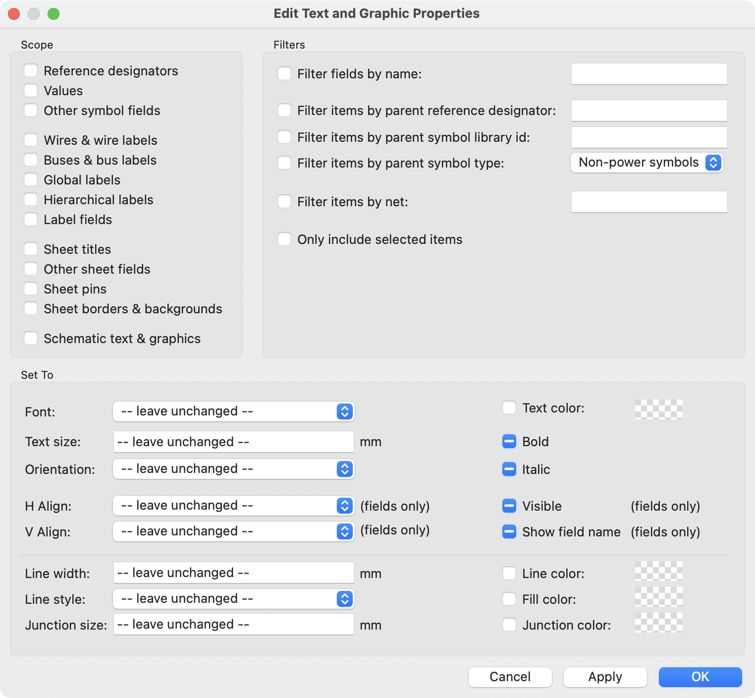
范围和筛选器
范围 设置限制了该工具只能编辑某些类型的对象。如果没有选择范围,就不会有任何东西被编辑。
Filters restrict the tool to editing particular objects in the selected scope.
Objects will only be modified if they match all enabled and relevant filters
(some filters do not apply to certain types of objects. For example, symbol
field filters do not apply to wires and are ignored for the purpose of changing
wire properties). If no filters are enabled, all objects in the selected scope
will be modified. For filters with a text box, wildcards are supported: *
matches any number of any characters, including none, and ? matches any single
character.
按名称过滤字段 过滤到指定的符号、标签或页面字段。
按父级位号筛选项目 过滤到具有指定位号的符号中的字段。通过父级符号库 ID 筛选到具有指定库位号的符号中的字段。*通过父级符号类型*筛选到选定类型(电源或非电源)的符号中的字段。
通过网络筛选项目 筛选到指定网络上的导线和标签。
只包括选定的项目 筛选器到当前选择。
可编辑的属性
被筛选对象的属性可以在对话框的底部设置为新值。
下拉列表和文本框可以被设置为 --保持不变-- 以保留现有值。复选框可以被选中或不被选中来启用或禁用一个变化,但也可以切换到第三个 "保持不变" 的状态。颜色属性必须被选中以改变值;棋盘式的色块表示颜色将从原理图设置或网络类属性的默认值中继承下来。
可以修改的文本属性有 字体、文本大小、文本方向(右/上/左/下)、水平 和 垂直对齐、文本颜色、强调(粗体*和*大写)以及字段和字段名的 可见度。
可以修改的图形和导线属性有:线宽、线样式(实线、虚线和点线)、线颜色、图形的 填充颜色,以及导线结点的 结点尺寸 和 结点颜色。
原理图标题块
标题块是用页面设置工具(![]() )编辑的。
)编辑的。
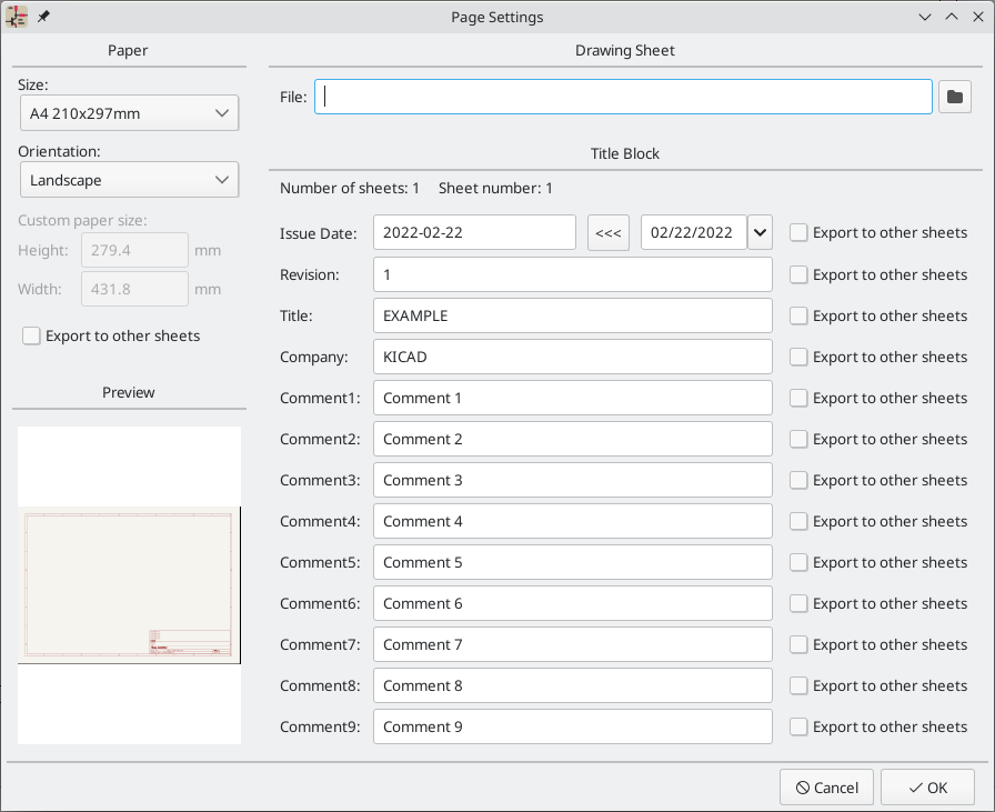
Each field in the title block can be edited, as well as the paper size and orientation. If the Export to other sheets option is checked for a field, that field will be updated in the title block of all sheets, rather than only the current sheet.
You can set the date to today’s or any other date by pressing the left arrow button next to Issue Date. Note that the date in the schematic will not be automatically updated.
也可以选择一个原理图模板文件。
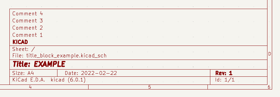
原理图编号(X/Y纸)会自动更新,但原理图页码也可以用 编辑 → 编辑原理图页码… 手动设置。
原理图设置
原理图设置窗口用于设置特定于当前活动原理图的原理图选项。例如,原理图设置窗口包含格式化选项、电气规则配置、网络类设置和原理图文本变量设置。
You can import schematic settings from an existing project using the Import Settings from Another Project… button. This allows you to choose a project to use as a template and select which settings to import (formatting preferences, field name templates, pin conflict map, violation severities, and net classes).
Schematic formatting
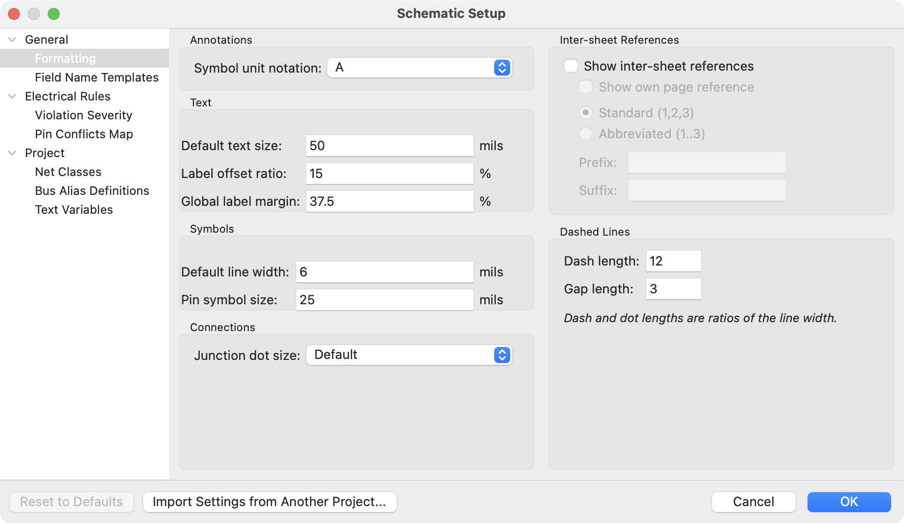
The formatting panel contains settings for the appearance of symbols, text, labels, graphics, and wires.
Symbol unit notation sets how each unit of a multi-unit symbol is referred to
in its reference designator. By default, a different letter for each unit is
appended to the reference designator with no separator, for example U1B for
the second unit of symbol U1, but this can be changed. Numbers can be used
instead of letters, and various separators can be used between the symbol
designator and the unit identifier (., -, _, or none).
Default text size sets the default text height used by the text, text box, and
label tools. Label offset ratio controls the vertical spacing between a local
label’s text and the attached wire, relative to the label’s text size. This also
affects the spacing between symbol pins and their pin number.
Global label margin defines the size of the box around a global label,
relative to the global label’s text size. Increasing the margin may be useful
to avoid overlapping text with overbars (~{}) or letters with descenders, but
this may cause closely packed global labels to overlap with each other.
Default line width sets the default line width for symbol graphics, if the symbol does not override the default line width. Pin symbol size scales symbol pin graphic style annotations, such as the bubble on an inverted pin.
Junction dot size sets the schematic’s default wire junction dot size. The default size can be overridden by editing an individual junction dot’s properties.
Show inter-sheet references enables or disables the display of
inter-sheet references, which are a list of page
numbers next to a global labels that link to other places in the schematic where
the same global label appears. Show own page reference controls whether the
current page is included in the list of page numbers. Standard and
abbreviated determine whether to display the complete list of page numbers or
only the first and last page numbers. The prefix and suffix fields add
optional characters before and after the list of page numbers. In the image
of an inter-sheet reference below, a prefix and suffix of [ and ],
respectively, have been added.
Dashed line appearance is controlled in the Formatting section. Dash length controls the length of dashes, while Gap length controls the spacing between dashes and dots. The dash and gap lengths are relative to the line width: a gap length of 2 means twice the width of the line.
Field name templates
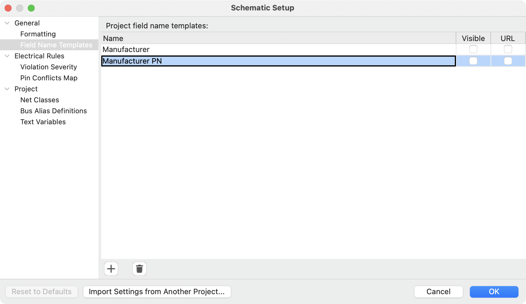
Field name templates are empty symbol fields that are automatically added to all symbols in the schematic. These can be useful when every symbol in the schematic needs additional fields beyond the fields that are defined in the library symbols, for example a field for the manufacturer’s part number.
Template fields can be set as visible or invisible, and can also be set as URL fields.
Field name templates that are defined in schematic setup apply only to the current project. Field name templates can also be defined in Preferences, which apply to all projects edited on your computer.
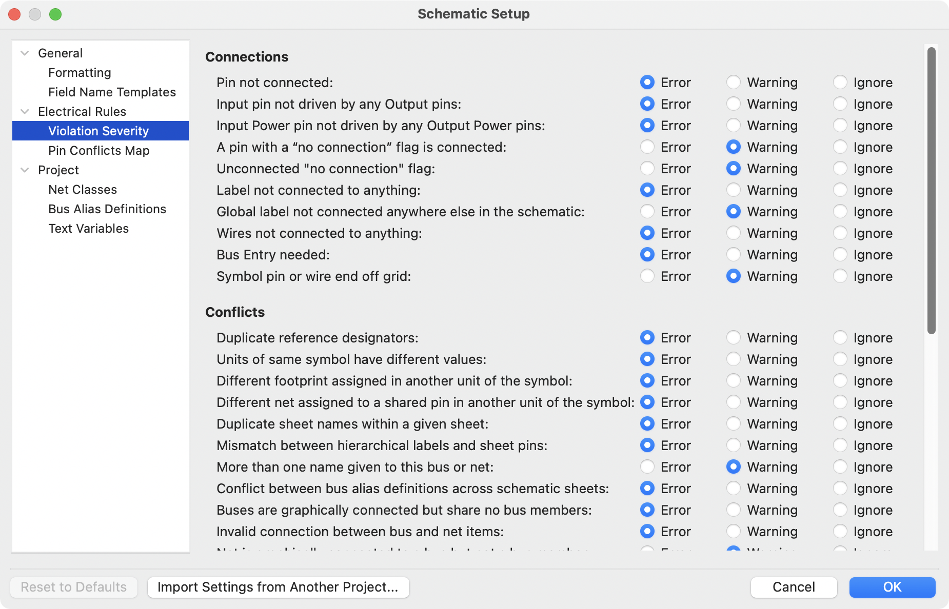
ERC violation severity and pin conflicts map
The Violation Severity panel lets you configure what types of ERC messages should be reported as Errors, Warnings, or ignored.
The Pin Conflicts Map allows you to configure connectivity rules to define electrical conditions for errors and warnings based on what types of pins are connected to each other. For example, by default an error is produced when an output pin is connected to another output pin.
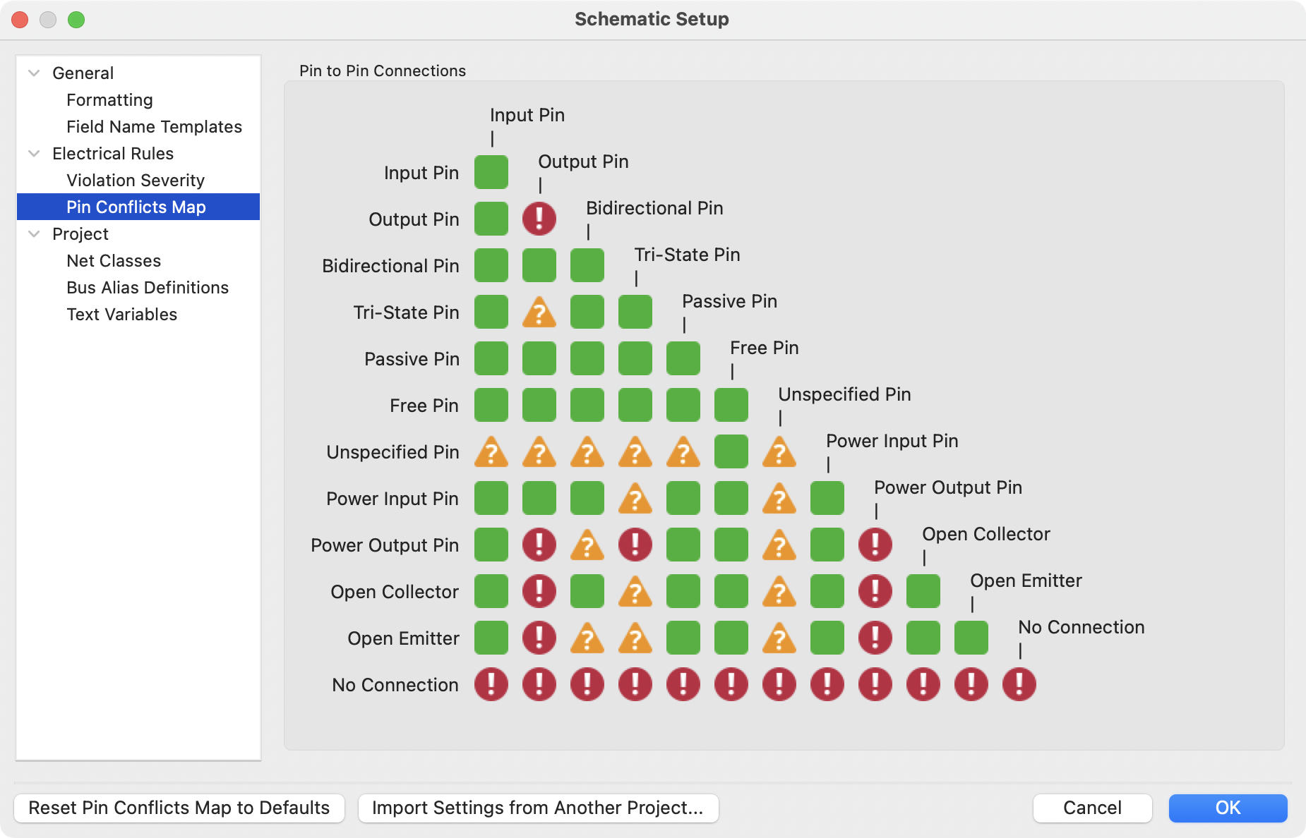
These panels are explained in more detail in the ERC section.
Net classes
The Net Classes panel allows you to manage netclasses for the project and assign nets to netclasses with patterns. Managing netclasses in this panel is equivalent to managing them in the Board Setup dialog. Nets can also be assigned to netclasses in the schematic using graphical assignments with net class directives or net labels.
Pattern-based netclass assigment is explained in more detail in the net classes section.
Bus alias definitions
The Bus Alias Definitions panel allows you to create bus aliases, which are names for groups of signals in a bus. For more information about bus aliases, see the bus alias documentation.
文本变量
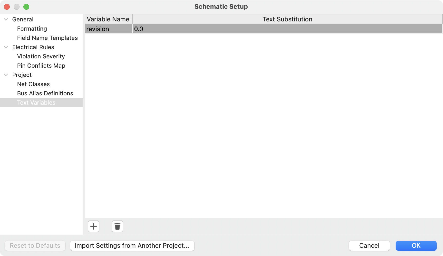
Text replacement variables can be created in the Text Variables section. These variables allow you to substitute the variable name for any text string. This substitution happens anywhere the variable name is used inside the variable replacement syntax of ${VARIABLENAME}.
For example, you could create a variable named VERSION and set the text substitution to 1.0. Now, in any text object on the PCB, you can enter ${VERSION} and KiCad will substitute 1.0. If you change the substitution to 2.0, every text object that includes ${VERSION} will be updated automatically. You can also mix regular text and variables. For example, you can create a text object with the text Version: ${VERSION} which will be substituted as Version: 1.0.
Text variables can also be created in Board Setup. Text variables are project-wide; variables created in the schematic editor are also available in the board editor, and vice versa.
There are also a number of built-in system text variables.
Opening legacy schematics
Modern versions of KiCad can always open projects created in older versions of KiCad. However, schematics created in some older versions of KiCad have special considerations that must be observed when opening them in order to prevent any data loss.
Opening KiCad 5.0 and 5.1 schematics
Modern versions of KiCad can open schematics created in versions prior to KiCad 6.0, but the cache library file (<projectname>-cache.lib) must be present to load the schematic correctly.
Since version 6.0, KiCad stores all symbols used in a project in the schematic. This means that you can open a schematic made in KiCad 6.0 or later on any computer, even if the libraries used in the project are not installed or have changed. Modern KiCad schematic files use the .kicad_sch extension.
Prior to version 6.0, KiCad did not store symbols in the schematic. Instead, KiCad stored references to the symbols and their libraries. It also stored a copy of every symbol used by the project in a separate cache library file (<projectname>-cache.lib). As long as the cache library was included with the project, the project could be distributed without the system library files, because KiCad could load any needed symbols from the cache library as a fallback if the libraries referenced in the schematic were missing. Legacy KiCad schematic files use the .sch extension.
When you open a legacy schematic, KiCad will look in the cache library to find all of the symbols used in the schematic in the cache library. When you save the legacy schematic, KiCad will save it as a new file in the modern schematic format (.kicad_sch), with the necessary symbols embedded in the schematic itself. The original legacy schematic and the cache library will remain, unmodified, but they are no longer necessary once the schematic has been saved in the modern format.
| Projects created in KiCad prior to version 6.0 must have a cache library. If the cache library is missing, the schematic will lose symbol information if the system symbol libraries are modified, reorganized, moved, or deleted. The libraries included with legacy versions of KiCad are substantially different than the modern KiCad libraries, so in practice KiCad will almost always fail to open legacy projects unless the cache library is present. |
When you open a legacy schematic, KiCad may display the Project Rescue Helper dialog. This means that one or more symbols in the cache library do not match the corresponding symbol in the external library. The dialog helps you "rescue" symbols from the cache library into your schematic, if desired. You can also open the rescue dialog at any time using Tools → Rescue Symbols…. The cache library file must be present in order to use the rescue tool.
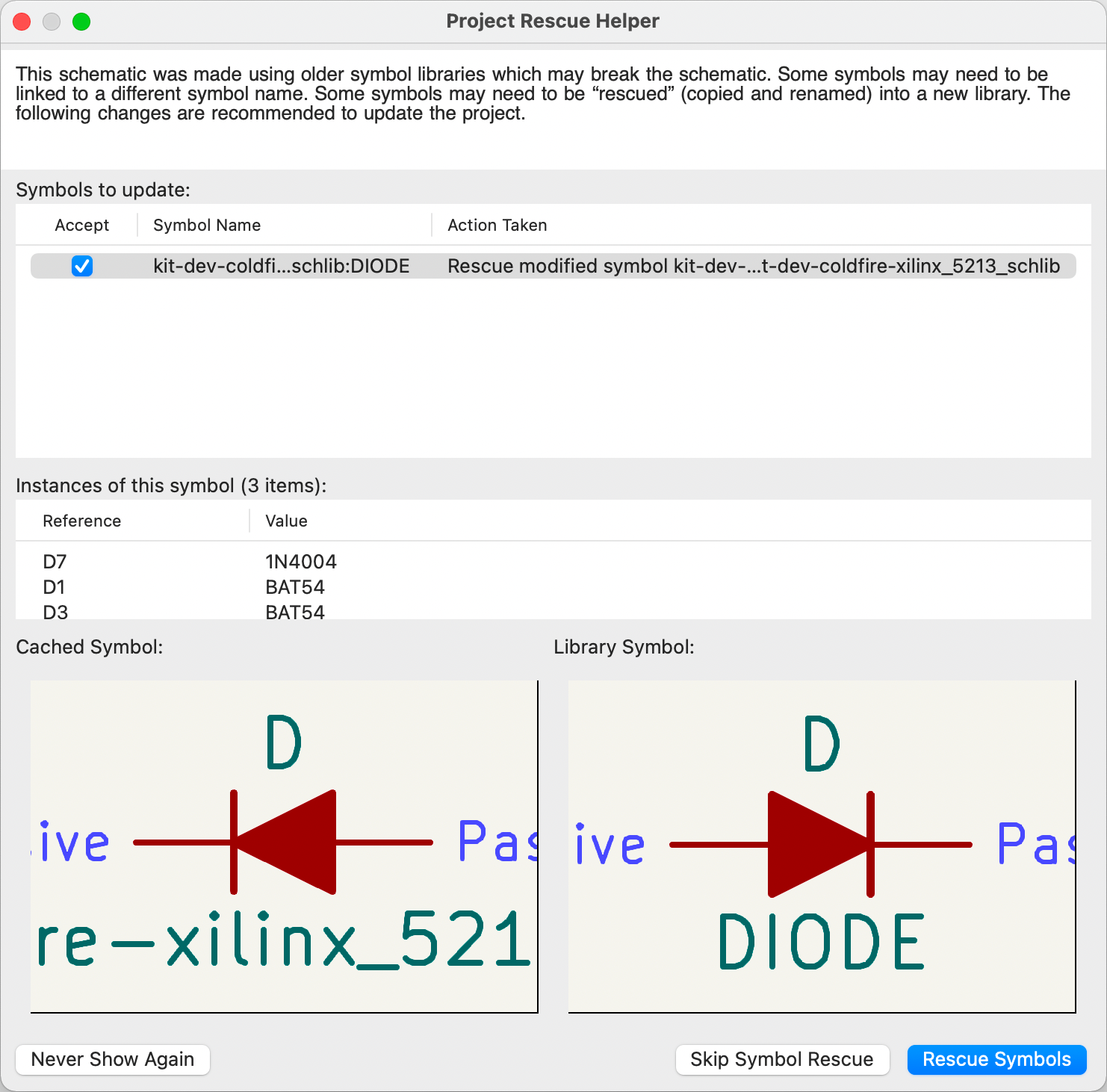
The rescue dialog lists all symbols that don’t match between the cache library and the external symbol library. The discrepancy can be because:
-
the cached symbol or the library symbol has been modified, so the two symbols no longer match, or
-
the cached symbol does not have a corresponding symbol in the symbol library, because the symbol or library was moved, renamed, deleted, or is not present on the current computer.
For each symbol in the list, selecting the symbol displays the reference designator and value for each instance of the symbol, and shows a visual preview of the symbol. If a corresponding symbol exists in the system symbol library, the dialog shows both copies of the symbol for comparison. If the symbol only exists in the cache library, the dialog only shows the cached symbol.
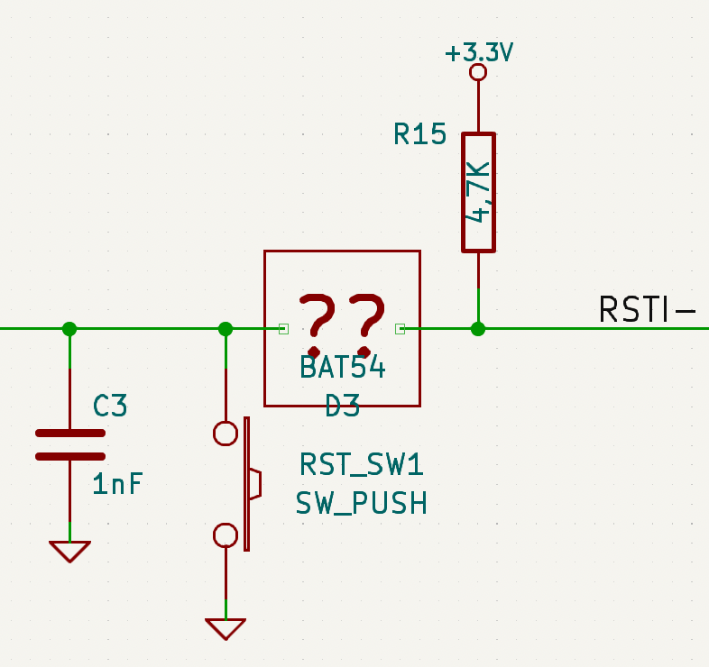
In this example, the project originally used a diode with the cathode facing left, but the library now contains one with the cathode facing right. This change would break the design, so it would be important to use the cached symbol as the original designer intended.
Pressing Rescue Symbols here will cause the selected symbols from the cache library to be saved into a special rescue library (<projectname>-rescue.kicad_sym). The corresponding symbols in the schematic will be updated to use the newly rescued symbols. Any unselected symbols will not be rescued, but their symbol linkage can be updated in the schematic later.
Alternatively, pressing Skip Symbol Rescue will exit the dialog without rescuing any symbols. KiCad will use the versions of the symbols found in the external libraries. You can run the rescue function again with Tools → Rescue Symbols…, or manually edit symbol linkage in the symbol’s properties.
If you would prefer not to see this dialog, you can press Never Show Again. This has the same effect as pressing Skip Symbol Rescue for the current schematic and all future schematics.
If a symbol in a legacy schematic cannot be found in either the cache library or the external library, KiCad cannot rescue that symbol. A placeholder symbol is inserted into the schematic in its place, as shown below.
You can attempt to remap these orphaned symbols using the Change Symbols or Edit Symbol Library Links dialogs, but either option may require manual corrections to the schematic. These tools are explained in more detail in the Updating and exchanging symbols section.
Opening pre-5.0 schematics
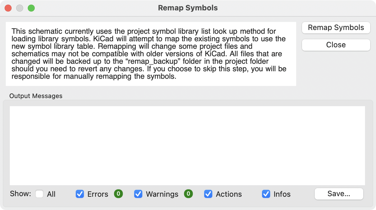
Modern versions of KiCad can open schematics created in versions prior to KiCad 5.0, but you will need to go through a symbol remapping process to open the schematic without losing symbol information.
Since version 5.0, KiCad schematics refer to specific symbols using both the symbol and library name. Even if multiple libraries each contain a symbol with the same name, the designer’s intended symbol is unambiguously specified.
Prior to version 5.0, KiCad schematics stored only the symbol name, not the library name. Symbols in the schematic were indirectly mapped back to the original library by searching through the project’s library list for a matching symbol. When you open a pre-5.0 schematic, KiCad will attempt to automatically "remap" the symbols so that each bare symbol name is replaced with a fully-specified symbol library and symbol name pair. The original schematics will be backed up in a rescue-backup folder.
You can skip the automatic remapping, but you will need to remap the symbols yourself using the Change Symbols dialog. You can also re-run the Remap Symbols tool using Tools → Remap Legacy Library Symbols….