检查电路板
测量工具
测量工具允许你在 PCB 上的各点之间进行距离和角度测量。 要激活该工具,请点击右侧工具栏的 ![]() 图标,或使用热键 Ctrl+Shift+M。 一旦该工具被激活,点击一次以设置测量起点,然后再点击一次以完成测量。
图标,或使用热键 Ctrl+Shift+M。 一旦该工具被激活,点击一次以设置测量起点,然后再点击一次以完成测量。
| 测量工具用于不需要永久显示的快速测量。 您所做的任何测量都将仅在该工具处于活动状态时显示。 要创建将显示在打印输出和打印中的永久性尺寸标注,请使用尺寸标注工具。 |
设计规则检查
设计规则检查器用于验证 PCB 是否符合电路板设置对话框中建立的所有要求,以及所有焊盘是否按照网表或原理图连接。 KiCad 可以在布线线段时自动防止一些违反设计规则的行为,但许多其他的行为是无法自动防止的。 这意味着在为 PCB 创建制造文件之前,必须使用设计规则检查器。
要使用设计规则检查器,请点击顶部工具栏的 ![]() 图标,或者从检查菜单中选择设计规则检查器。
图标,或者从检查菜单中选择设计规则检查器。
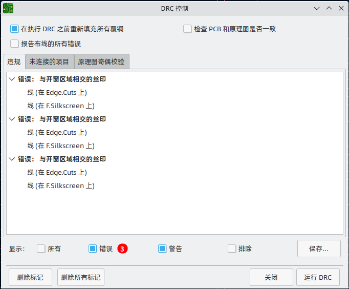
DRC 控制窗口的顶部部分包含一些控制设计规则检查器的选项:
重新填充所有敷铜后再执行 DRC: 启用后,每次运行设计规则检查器时都会重新填充敷铜。 如果未手动重新填充敷铜,禁用此选项可能会导致错误的 DRC 结果。
报告每个布线的所有错误: 启用后,将报告每个线段的所有间隙错误。 禁用时,将只报告第一个错误。 启用此选项将导致设计规则检查器运行速度变慢。
测试 PCB 和原理图之间的奇偶校验: 启用后,设计规则检查器除了测试 PCB 设计规则外,还将测试原理图和 PCB 之间的差异。 在独立模式下运行 PCB 编辑器时,该选项不起作用。
运行 DRC 后,任何违规行为都会显示在 DRC 控制窗口的中间部分。 违反规则、未连接的项目以及原理图和 PCB 之间的差异会显示在三个不同的标签中。 违规列表下面的控件可以用来显示或隐藏违规,这取决于其严重程度。 在运行 DRC 后,可以使用保存按钮创建一个纯文本格式的报告文件。
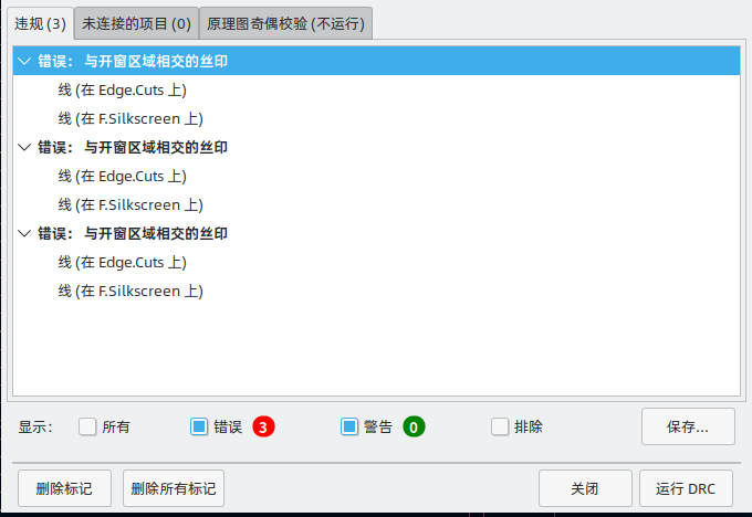
每项违规行为涉及 PCB 上的一个或多个对象。 在违章列表中,涉及的对象列在违章下面。 点击列表中的违规行为将移动 PCB 编辑器的视图,使受影响的区域居中。 点击违章所涉及的对象之一将突出显示该对象。
右键单击列表视图中的违规行为将打开一个上下文菜单,其中包括排除所选违规行为的额外操作。 除非 DRC 控制窗口底部的 "排除" 复选框被激活,否则排除的违反行为会被隐藏。 被排除的违规行为在设计规则检查器运行期间会被记住。
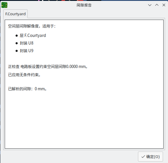
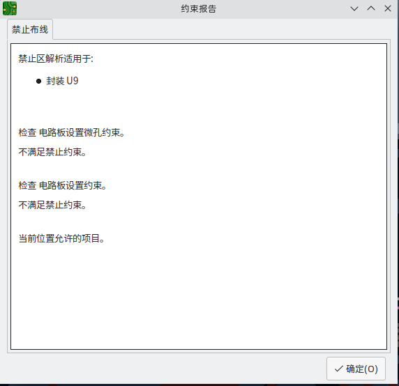
间隙和约束解析
间隙和约束解决工具允许你检查哪些间隙和设计约束规则适用于选定的项目。 当设计具有复杂设计规则的 PCB 时,这些工具可以提供帮助,因为在这种情况下并不总是清楚哪些规则适用于某个对象。
要检查两个对象之间适用的间隙规则,选择这两个对象并从检查菜单中选择间隙分辨率。 间隙报告对话框将显示每个铜层上的对象之间所需的间隙,以及产生该间隙的设计规则。
To inspect the design constraints that apply to an object, select it and choose Constraints Resolution from the Inspect menu. The Constraints Report dialog will show any constraints that apply to the object.
Find tool
The Find tool searches for text in the PCB, including reference designators, footprint fields, and graphic text. When the tool finds a match, the canvas is zoomed and centered on the match and the text is highlighted. Launch the tool using the (![]() ) button in the top toolbar.
) button in the top toolbar.
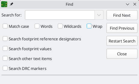
The Find tool has several options:
Match case: Selects whether the search is case-sensitive.
Words: When selected, the search will only match the search term with complete words in the PCB. When unselected, the search will match if the search term is part of a larger word in the PCB.
Wildcards: When selected, wildcards can be used in the search terms. ?
matches any single character, and * matches any number of characters. Note
that when this option is selected, partial matches are not returned: searching
for abc* will match the string abcd, but searching for abc will not.
Wrap: When selected, search results will return to the first hit after reaching the last hit.
Search footprint reference designators: Selects whether the search should apply to footprint reference designators.
Search footprint values: Selects whether the search should apply to footprint value fields.
Search other text items: Selects whether the search should apply to other text items, including graphical text and footprint fields other than value and reference.
Search DRC markers: Selects whether the search should apply to the violation descriptions of DRC markers shown on the board.
3D 查看器
The 3D Viewer shows a 3-dimensional view of the board and the components on the board. You can view the board from different perspectives, show or hide different types of components, cross-probe from the PCB Editor to the 3D viewer, and generate raytraced renders of the board.
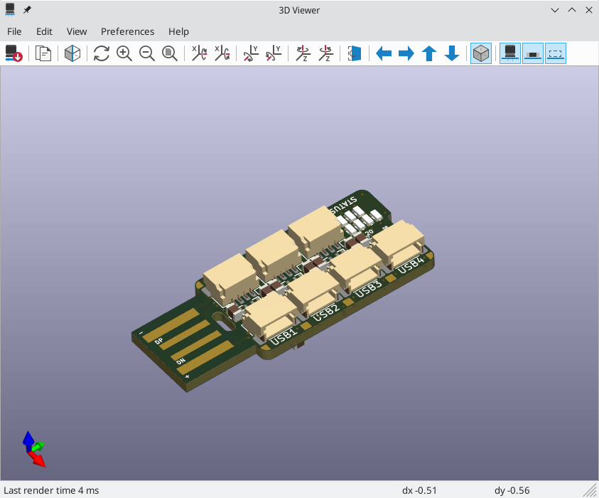
| The 3D model for a component will only appear if the 3D model file exists and has been assigned to the footprint. |
| Many footprints in KiCad’s standard library do not yet have model files created for them. However, these footprints may contain a path to a 3D model that does not yet exist, in anticipation of the 3D model being created in the future. |
Navigating the 3D view
Dragging with the left mouse button will orbit the 3D view around the centroid of the board. Scrolling the mouse wheel will zoom the view in or out. Scrolling while holding Ctrl pans the view left and right, and scrolling while holding Shift pans up and down. Dragging with the middle mouse button also pans the view.
Different sized 3D grids can be set using the Preferences → 3D Grid menu. Bounding boxes for each component can be enabled with Preferences → Show Model Bounding Boxes.
When the PCB Editor and the 3D Viewer are both open, selecting a footprint in the PCB Editor will also highlight the component in the 3D Viewer. The highlight color is adjustable in Preferences → Preferences… → 3D Viewer → Realtime Renderer → Selection Color.
Generating images with the 3D Viewer
The current 3D view can be saved to an image with File → Export Current View as PNG… or Export Current View as JPG…, depending on the desired image format. The current view can also be copied to the clipboard using the ![]() button, or Edit → Copy 3D Image.
button, or Edit → Copy 3D Image.
The 3D Viewer has a raytracing rendering mode which displays the board using a more physically accurate rendering model than the default rendering mode. Raytracing is slower than the default rendering mode, but it can be used when the most visually attractive results are desired. Raytracing mode is enabled with the ![]() button, or with Preferences → Raytracing. The 3D grid and selection highlights are not shown in raytracing mode.
button, or with Preferences → Raytracing. The 3D grid and selection highlights are not shown in raytracing mode.
Colors and other rendering options, for both raytraced and non-raytraced modes, can be adjusted in Preferences → Preferences… → 3D Viewer.
3D viewer controls
Many viewing options are controlled with the top toolbar.
|
Reload the 3D model |
|
Copy 3D image to clipboard |
|
Render current view using raytracing |
|
Zoom in |
|
Zoom out |
|
Redraw |
|
Fit drawing in display area |
|
Rotate X clockwise |
|
Rotate X counterclockwise |
|
Rotate Y clockwise |
|
Rotate Y counterclockwise |
|
Rotate Z clockwise |
|
Rotate Z counterclockwise |
|
Flip board view |
|
Pan board left |
|
Pan board right |
|
Pan board up |
|
Pan board down |
|
Enable/disable orthographic projection |
|
Show/hide 3D models for through-hole components |
|
Show/hide 3D models for surface mount components |
|
Show/hide 3D models for components of type 'other' |
网络检查
网络检查器允许你查看电路板中所有网络的统计数据。 要打开检查器,请点击外观面板中的网络部分顶部的 ![]() 图标,或者从检查菜单中选择网络检查器。
图标,或者从检查菜单中选择网络检查器。
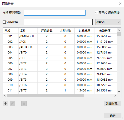
点击网络列表中的一个网络会在电路板上高亮显示该网络。 单击列标题允许您按该列对网络列表进行排序。
分组依据字段允许您将不同的网络组合在一起,并查看组合的网络的总长度。 例如,如果您有两个名为 DATA0 和 DATA0_EXT 的网络,则使用值为 DATA0* 的分组依据将创建一个包含这两个网络的组。 通过将分组依据模式从通配符更改为 RegEx (正则表达式),可以创建更复杂的分组。 分组依据模式的子字符串 (Substr) 变体将为以不同方式匹配该模式的每组网络创建组。
例如,如果您有 U1D+,U1D-,U2D+ 和 U2D-,分组模式 U*D 将在通配符模式下匹配所有四个网络,创建一个单一的组 U*D。 在通配符子串模式下,它将匹配所有四个网络,但创建两个不同的组:U1D 和 U2D。
Pad Count and Via Count show the number of pads (surface mount and through hole) and vias on a net. Via Length shows the total height of each via (not accounting for which copper layers the via connects to). In other words, Via Length is equal to Via Count multiplied by the stackup height of the board. Track Length shows the total length of all track segments in a net, not accounting for topology. Die length shows the total of all Pad to Die Length values set for pads on the net.
| 网络检查器中显示的长度不同于长度调整工具中显示的长度, 因为网络检查器显示连接到网络的所有布线的总和, 而长度调整工具显示最近的两个焊盘或分支过孔之间的距离。 有关长度调整工具的更多信息,请参见布线部分。 |