编辑电路板
放置和绘制操作
放置和绘图工具位于右边的工具栏中。 当一个工具被激活时,它将一直处于激活状态,直到选择了一个不同的工具或用 Esc 键取消该工具。 当任何其他工具被取消时,选择工具总是被激活。
某些工具栏按钮在调色板中有多个可用工具。这些工具由按钮右下角的小箭头表示:
要显示调色板,你可以在工具上点击并按住鼠标按钮,或者点击并拖动鼠标。 调色板关闭时将显示最近使用的工具。
|
Selection tool (the default tool). |
|
Local ratsnest tool: when the board ratsnest is hidden, selecting footprints with this tool will show the ratsnest for the selected footprint only. Selecting the same footprint again will hide its ratsnest. The local ratsnest setting for each footprint will remain in effect even after the local ratsnest tool is no longer active. |
|
Footprint placement tool: click on the board to open the footprint chooser, then click again after choosing a footprint to confirm its location. |
|
Route tracks / route differential pairs: These tools activate the interactive router and allow placing tracks and vias. The interactive router is described in more detail in the Routing Tracks section below. |
|
Tune length: These tools allow you to tune the length of single tracks or the length or skew of differential pairs, after they have been routed. See the Routing Tracks section for details. |
|
Add vias: allows placing vias without routing tracks. Vias placed on top of tracks using this tool will take on the net of the closest track segment and will become part of that track (the via net will be updated if the pads connected to the tracks are updated). Vias placed anywhere else will take on the net of a copper zone at that location, if one exists. These vias will not automatically take on a new net if the net of the copper zone is changed. |
|
Add filled zone: Click to set the start point of a zone, then configure its properties before drawing the rest of the zone outline. Zone properties are described in more detail below. |
|
Add rule area: Rule areas, formerly known as keepouts, can restrict the placement of items and the filling of zones and can also define named areas to apply specific custom design rules to. |
|
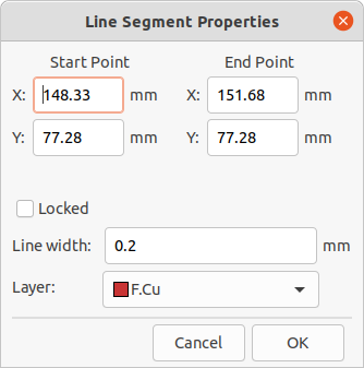
Draw lines. Note: Lines are graphical objects and are not the same as tracks placed with the Route Tracks tool. Graphical objects cannot be assigned to a net. |
|
Draw arcs: pick the center point of the arc, then the start and end points. |
|
Draw rectangles. Rectangles can be filled or outlines. |
|
Draw circles. Circles can be filled or outlines. |
|
Draw graphical polygons. Polygons can be filled or outlined. Note: Filled graphical polygons are not the same as filled zones: graphical polygons cannot be assigned to a net and will not keep clearance from other items. |
|
Add text. |
|
Add dimensions. Dimension types are described in more detail below. |
|
Add layer alignment mark. |
|
Deletion tool: click objects to delete them. |
|
Set drill/place origin. Used for fabrication outputs. |
|
Set grid origin. |
捕捉
移动、拖动和绘制电路板元素时,栅格、焊盘和其他元素可以具有捕捉点,具体取决于用户偏好设置中的设置。在复杂的设计中,捕捉点可能离得太近,这会使当前的工具操作变得困难。使用下表中的快捷键可以在移动鼠标时禁用栅格和对象捕捉。
| 快捷键 | 效果 |
|---|---|
Ctrl |
关闭网格捕捉。 |
Shift |
关闭对象捕捉。 |
编辑对象属性
所有对象都有可在对话框中编辑的属性。 使用热键 E 或从右键菜单中选择属性来编辑所选项目的属性。 只有当你选择的所有项目都是同一类型时,你才能打开属性对话框。 要想一次编辑不同类型的项目的属性,请参阅下面关于批量编辑工具的章节。
在属性对话框中,任何包含数字值的字段也可以接受一个基本的数学表达式,从而得到一个数字值。 例如,一个尺寸可以被输入为 2 * 2mm,结果是 4mm 的值。 支持基本算术运算符以及用于定义运算顺序的圆括号。
使用封装
| TODO: 编写这一节—包括封装属性,从库中更新,等等。 |
使用焊盘
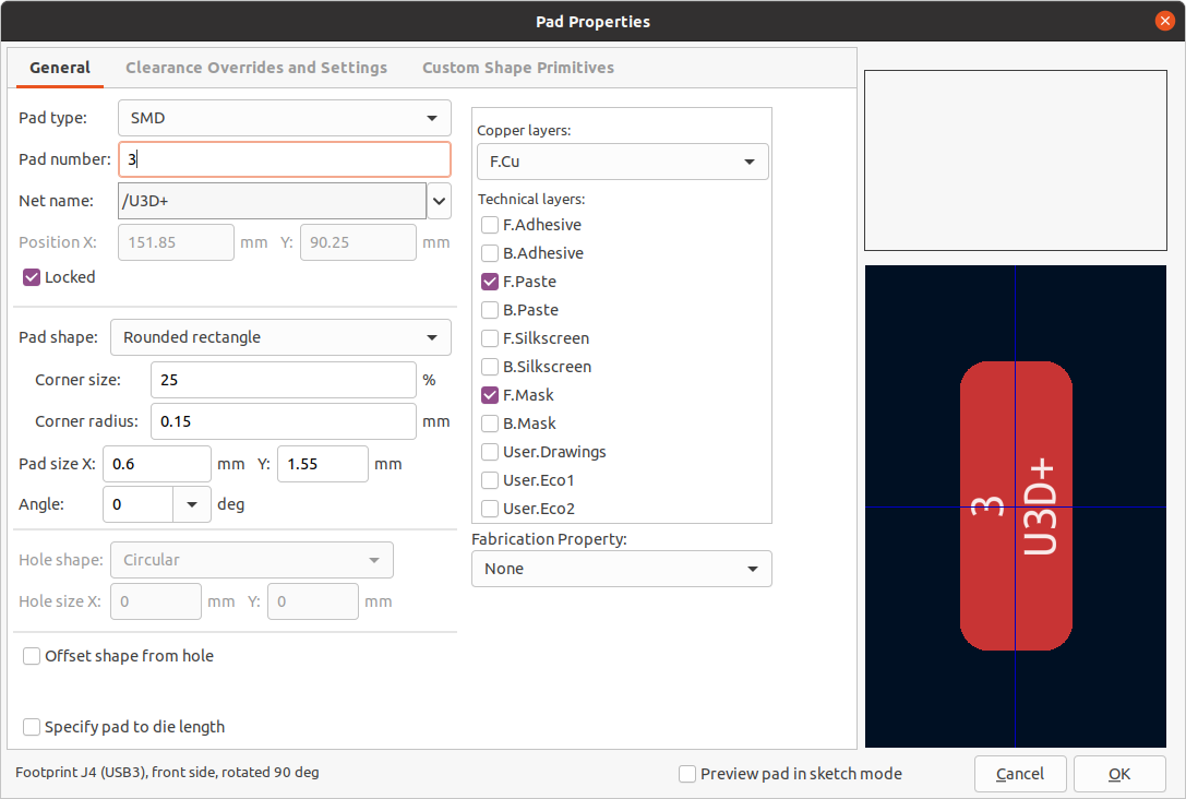
The properties of each individual pad of a footprint can be inspected and edited after placing the footprint on the board. In other words, it is possible to override the design of an individual footprint pad in a specific instance of the footprint on the board, if the footprint design in the library is not appropriate. For example, you may wish to remove the solder paste aperture for a pad that needs to remain unsoldered in a specific design, or you may wish to move the location of a through-hole pad for an axial-lead resistor in order to fit a specific design.
| By default, the position of all footprint pads are locked, so it is possible to edit the pad properties but not move the pad’s location relative to the rest of the footprint. Pads may be unlocked to allow free movement, which can be useful for certain applications (such as through-hole footprints with varying lead positions) but is generally never recommended for surface-mount footprints. |
The pad properties dialog is opened through the context menu or default hotkey E when a pad is selected. Note that KiCad assumes that if you click near a pad, you are probably trying to select the entire footprint rather than a single pad. To select a single pad, make sure to click inside the pad area, or turn off the Footprints setting in the selection filter (and make sure the Pads setting is turned on) to prevent accidental selection of the entire footprint rather than a specific pad.
The General tab of the pad properties dialog shows the physical properties of the pad, including its geometry, shape, and layer settings.
Pad type: this setting controls which features are enabled for the pad:
SMD pads are electrically-connected and have no hole. In other words, they exist on a single copper layer.
Through-hole pads are electrically-connected and have a plated hole. The hole exists on every layer, and the copper pad exists on multiple layers (see Copper layers setting below).
Edge Connector pads are SMD pads that are allowed to overlap the board outline on the Edge.Cuts layer.
NPTH, Mechanical pads are non-plated through holes that do not have an electrical connection.
SMD Aperture pads are pads that have no hole and no electrical connection. These can be used to add specific designs to a technical layer, for example a paste or solder mask aperture.
The Copper layers setting controls which copper layers will have a shape associated with the pad.
For SMD pads, the options are F.Cu or B.Cu, controlling whether the pad sits on the front or the back of the board relative to the footprint’s location. In other words, if a pad is set to exist on B.Cu in its properties, and the footprint is flipped to the back of the board, that pad will now exist on F.Cu, because it also has been flipped.
For through-hole pads, it is possible to remove the pad shape from copper layers where the pad is not electrically connected to other copper (tracks or filled zones). Setting the copper layers to connected layers only will remove the pad shape from any unconnected layers, and setting to F.Cu, B.Cu, and connected layers will remove the pad shape from any internal unconnected layers. This can be useful in dense board designs to increase the routable area on internal layers.
The Technical layers checkboxes control which technical layers will have an aperture added with the pad’s shape. By default, pads have apertures on the paste and mask layers matching their copper layer.
| It is not possible to define a different pad shape or size on different copper layers in the current version of KiCad. |
Specify pad to die length: This setting allows a length to be associated with this pad that will be added to the routed track length by the track length tuning tools and the Net Inspector. This can be used to specify internal bondwire lengths for more accurate length matching, or in other situations where the electrical length of a net is longer than the length of the routed tracks on the board.
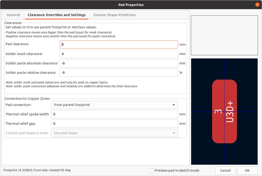
The aperture appearing on any technical layer will have the same shape and size as the pad shape on the copper layer(s). In the PCB manufacturing process, the manufacturer will often change the relative size of mask and paste apertures relative to the copper pad size, but since this size change is specific to a manufacturing process, most manufacturers expect the design data to be provided with the apertures set to the same size as the copper pads. For specific situations where you need to oversize or undersize a technical layer aperture in the design data, you can use the settings in the Overrides tab.
Pad clearance controls the minimum clearance between the pad and any copper shape (tracks,
vias, pads, zones) on a different net. This value is normally set to 0 which will cause the pad
clearance to be inherited from any clearance override set on the footprint, or the board’s design
rules and netclass rules if the footprint clearance is also set to 0.
Solder mask clearance controls the size difference between the pad shape and the aperture shape
on the F.Mask and B.Mask layers. A positive number means the solder mask aperture will be larger
than the copper shape. This number is an inflation applied to all directions. For example, a
value of 0.1mm here will cause the solder mask aperture to be inflated by 0.1mm, meaning that
there will be an 0.1mm border on all sides of the pad and the solder mask opening will be 0.2mm
wider than the pad when measured along a given axis.
Solder paste absolute clearance controls the size difference between the pad shape and the aperture shape on the F.Paste and B.Paste layers. Its behavior is otherwise identical to the behavior of the solder mask clearance setting.
Solder paste relative clearance allows setting a solder paste clearance value as a percentage of the pad size rather than an absolute distance value. If both relative and absolute clearances are specified, they are added together to determine the solder paste aperture size.
The Overrides tab also has controls for how the pad connects to any copper zone that overlaps it and shares its net.
Pad connection controls whether the pad will have a solid, thermal relief, or no connection to the zone. Like the other overrides, this one may be set for an individual pad or for an entire footprint. The default setting for this control is From parent footprint, and the default footprint setting is to use the connection mode specified in the zone properties.
Thermal relief spoke width controls the width of the spokes generated when the zone connection mode is Thermal Relief.
Thermal relief gap controls the length of the thermal spokes, or the gap between the pad’s shape and the filled copper area of the zone.
Custom pad shape in zone controls the behavior of the zone filler when the pad uses a custom shape rather than one of the default shapes. This can be used to achieve different results when using thermal reliefs and custom pad shapes.
使用区域
Copper zones, also sometimes called copper pours or fills by other EDA tools, are solid or hatched areas of copper assigned to a particular net that automatically keep clearance from other copper objects. Zones are commonly used to fill in all free space on a board layer (or a portion of a layer) in order to create ground and power planes, carry high currents, or to provide shielding.
| Some EDA tools have separate tools for creating "plane layers" and for creating copper zones on signal layers. In KiCad, the Copper Zone tool is used for both these applications. |
Zones are defined by a polygonal outline that defines the maximum extent of the filled copper area. This outline does not represent physical copper and will not appear in exported manufacturing data. The actual copper areas of the zone must be filled each time the outline, or any objects inside the outline, are modified. The filling process may be run on a single zone, or on all zones in a board (default hotkey B). Zones may be unfilled (default hotkey Ctrl+B) to improve performance and reduce visual clutter while editing large boards.
| Zone filling is a manual process rather than occurring every time an object changes that would result in a change to the zone copper. This is because zone filling can be a slow process on older computers or very large designs. It is important to make sure zone fills are up-to-date before generating outputs. KiCad will check that zones have been updated and warn you before generating outputs or running DRC when zones have not yet been refilled. |
To draw a zone, click the Add Filled Zone tool (![]() ) on the right toolbar, or use default hotkey Ctrl+Shift+Z. Click to choose the first point of the zone outline. The Zone Properties dialog will appear, allowing you to choose the zone net and other properties. These properties may be edited at any time, so it is not critical to choose them all correctly at first. Accept the dialog and continue placing points to define the zone outline. To finish the zone, double-click to set the last point. Zone outline points may be modified like graphic polygons, by dragging the square handles to move a corner or dragging the circular handles to move an edge. To edit the zone’s properties, use hotkey E or select Properties from the context menu.
) on the right toolbar, or use default hotkey Ctrl+Shift+Z. Click to choose the first point of the zone outline. The Zone Properties dialog will appear, allowing you to choose the zone net and other properties. These properties may be edited at any time, so it is not critical to choose them all correctly at first. Accept the dialog and continue placing points to define the zone outline. To finish the zone, double-click to set the last point. Zone outline points may be modified like graphic polygons, by dragging the square handles to move a corner or dragging the circular handles to move an edge. To edit the zone’s properties, use hotkey E or select Properties from the context menu.
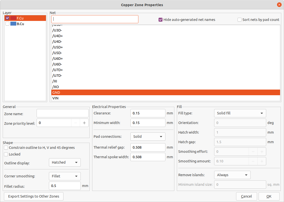
Layer: A single zone object can create filled copper on one or more copper layers. Check the box next to each copper layer that this zone outline should fill on. The copper on each layer will be filled independently, but all layers will share the same net.
Net: Select the electrical net that the zone copper should be connected to. It is possible to create zones with no net assignment. Zones with no net will keep clearance from any copper objects on any net.
Zone name can be used to assign a specific name to a zone. This name can be used to refer to the zone in custom DRC rules.
Zone priority level determines the order in which multiple zones on a single layer are filled. The highest priority level zone on a given layer will be filled first. Lower-priority zones will keep clearance to the filled areas of higher-priority zones. Two zones on the same layer with the same priority level will overlap (short-circuit) with each other.
| Zones with the same priority level will never keep clearance from each other, even if they are assigned to different nets! The design rule checker will report these short-circuits, but they will not be prevented by the zone filler. |
Constrain outline to H, V and 45 degrees controls the initial behavior of the zone outline drawing tool. When this option is enabled, the zone outline will be restricted to 45-degree angles. Note that after the zone outline has been created, this option has no effect. Outline points may be modified freely after creation.
Locked controls whether or not the zone outline object is locked. Locked objects may not be manipulated or moved, and cannot be selected unless the Locked Items option is enabled in the Selection Filter panel.
Outline display controls how the zone outline is drawn on screen. In Line mode, only the border lines of the outline are drawn. In Hatched mode, hatch lines are drawn on the inside of the outline border for a short distance, to make the zone outline more apparent. In Fully Hatched mode, hatch lines are drawn across the entire inside of the zone outline.
Corner smoothing controls the behavior of the filled copper areas at corners of the outline. Corners can be smoothed by a chamfer or fillet, or can extend all the way to the outline corner if smoothing is disabled.
| By default, chamfers and fillets are not added to inside corners of the zone outline, because this would result in filled copper extending outside the outline. If smooth inside corners are desired, enable the Allow fillets outside zone outline option in the Constraints section of the Board Setup dialog. |
Clearance controls the minimum clearance the filled areas of this zone will keep from other copper objects. Note that if two clearance values are in conflict, the larger clearance value will be used. For example, if a zone is set to use 0.2mm clearance but its netclass is set to use 0.3mm clearance, the result will be an 0.3mm clearance.
Minimum width controls the minimum size of narrow necks of copper created inside the zone. Any copper areas that would be below this minimum width are removed during the filling process.
Pad connection controls the way that the filled zone areas will connect to footprint pads on the same net. Solid connections will result in the copper completely overlapping the pads. Thermal reliefs will result in small copper spokes connecting the pad to the rest of the copper zone, increasing the thermal resistance between the pad and the rest of the zone. This can be useful for hand soldering. Reliefs for PTH will apply thermal reliefs to plated through-hole pads and use solid connections for surface mount pads. None will result in the zone not connecting to any pads on the same net.
Thermal relief gap controls the distance maintained between any pad and the copper zone when the pad connection mode is set to generate thermal reliefs.
Thermal spoke width controls the width of the "spokes", or short copper segments connecting the pad to the rest of the copper zone.
Fill type controls how the copper zone is filled: the default is solid fill, which will result in copper filling in all available space within the zone outline. The zone can also be set to fill a hatch pattern, which will fill the area with a pattern that contains less copper. This can be useful for flexible printed circuits and other specialty applications.
Orientation controls the angle of the hatch pattern lines. An orientation of 0 degrees will result in the hatch pattern using horizontal and vertical lines.
Hatch width controls the width of each line in the hatch pattern.
Hatch gap controls the distance between each line in the hatch pattern.
Smoothing effort controls the style of smoothing applied to the hatch pattern. A value of 0 will result in no smoothing, and a value of 3 will result in the finest smoothing. Higher values will result in longer processing time and larger Gerber files.
Smoothing amount is a ratio that controls the size of the smoothing chamfers or fillets that are generated when smoothing effort is set to a value other than 0. An amount of 0.0 results in no smoothing, and a value of 1.0 results in maximum smoothing (in other words, a chamfer or fillet equal to half of the hatch gap).
Remove islands controls the behavior of isolated copper areas, also called islands, after the initial zone fill. When this is set to always, isolated areas inside the zone are removed. When set to never, isolated areas are left alone, and will result in copper areas that are not connected to the rest of the net. When set to below area limit, a minimum island size can be specified, and islands below this threshold will be removed.
图形对象
图形对象 (直线、圆弧、矩形、圆、多边形和文本)可以存在于任何图层上,但不能分配给网络。矩形、圆和多边形可以在其属性对话框中设置为填充或轮廓。线宽属性将控制轮廓的宽度,即使是填充形状也是如此。填充形状的线宽可以设置为 "0" 以禁用轮廓。
正在创建图形形状
The right toolbar can be used to create lines (![]() , default hotkey Ctrl+Shift+L), arcs (
, default hotkey Ctrl+Shift+L), arcs (![]() , default hotkey Ctrl+Shift+A), rectangles (
, default hotkey Ctrl+Shift+A), rectangles (![]() ), circles (
), circles (![]() , default hotkey Ctrl+Shift+C), and polygons (
, default hotkey Ctrl+Shift+C), and polygons (![]() , default hotkey Ctrl+Shift+P).
, default hotkey Ctrl+Shift+P).
Rectangles, circles, and polygons can be filled shapes or outlines. The line width option controls the width of the outline. The outline width extends on both sides of the "ideal" shape of the graphic object. For example, a graphic circle that is defined to have 2mm radius and 0.2mm line width will consist of a torus with an outer radius of 2.2mm and inner radius of 1.8mm. If the filled shape option is enabled and the line width is set to 0, the shape will be a filled circle with 2mm radius.
正在创建文本对象
Graphical text may be placed by using the (![]() ) icon in the right toolbar or by keyboard shortcut Ctrl+Shift+T. Click to place the text origin, and then edit the text and its properties in the dialog that will appear:
) icon in the right toolbar or by keyboard shortcut Ctrl+Shift+T. Click to place the text origin, and then edit the text and its properties in the dialog that will appear:
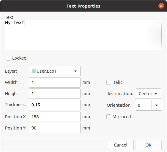
Text may be placed on any layer, but note that text on copper layers cannot be associated with a net and cannot form connections to tracks or pads. Copper zones will fill around the rectangular bounding box of text objects.
电路板轮廓 (边缘切割)
KiCad 使用 Edge.Cuts 层上的图形对象来定义电路板的轮廓。 该轮廓必须是一个连续(封闭)的形状,但可以由不同类型的图形对象组成,如线和弧,或者是一个单一的对象,如矩形或多边形。 如果没有定义电路板的轮廓,或者电路板的轮廓无效,那么一些功能,如 3D 查看器和一些设计规则的检查将无法发挥作用。
标注
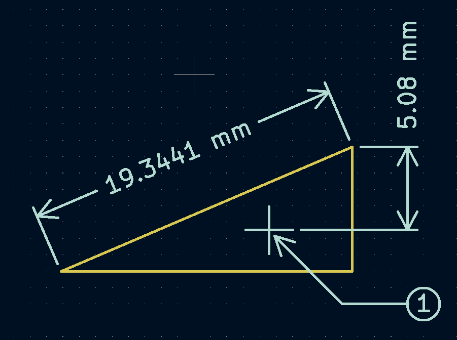
标注是用于显示测量值或电路板设计上的其他标记的图形对象。 它们可以被添加到任何绘图层中,但通常被添加到用户层之一。 KiCad 目前支持四种不同类型的标注:对齐、正交、中心和引线。
对齐 标注 (![]() ) 表示两点之间距离的测量。
测量轴是连接这两个点的线,标注图形与该轴保持平行。
) 表示两点之间距离的测量。
测量轴是连接这两个点的线,标注图形与该轴保持平行。
正交 标注 (![]() ) 也测量两点之间的距离,但测量轴是 X 轴或 Y 轴。
换句话说,这些标注表示两点之间距离的水平或垂直分量。
创建正交标注时,在选择要测量的两个点后,可以根据放置标注的位置选择要用作测量轴的轴。
) 也测量两点之间的距离,但测量轴是 X 轴或 Y 轴。
换句话说,这些标注表示两点之间距离的水平或垂直分量。
创建正交标注时,在选择要测量的两个点后,可以根据放置标注的位置选择要用作测量轴的轴。
中心 标注 (![]() ) 创建一个十字标记来指示一个点或圆或圆弧的圆心。
) 创建一个十字标记来指示一个点或圆或圆弧的圆心。
引线 标注 (![]() ) 创建一个箭头,将一条引线连接到文本字段。
此文本字段可以包含任何文本以及文本周围的可选圆形或矩形框。
这种类型的标注通常用来提醒人们注意设计的某些部分,以便在制造说明中参考。
) 创建一个箭头,将一条引线连接到文本字段。
此文本字段可以包含任何文本以及文本周围的可选圆形或矩形框。
这种类型的标注通常用来提醒人们注意设计的某些部分,以便在制造说明中参考。
创建一个标注后,可以编辑其属性(热键 E)以改变显示数字的格式以及文本和图形线的风格。
| 您可以在电路板设置对话框的文本和图形默认值部分自定义新创建的标注对象的默认样式。 |
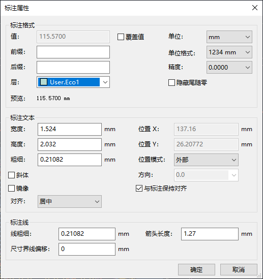
标注格式选项
覆盖值: 启用后,您可以直接在 值 字段中输入测量值,而不是实际测量值。
前缀: 此处输入的任何文字都将显示在测量值之前。
后缀: 此处输入的任何文字都将显示在测量值之后。
图层: 选择标注对象存在的层。
单位: 选择显示测量值的单位。 当更改电路板编辑器的显示单位时,自动 单位会导致标注单位发生变化。
单位格式: 从几种内置的单位显示风格中选择。
精度: 选择要显示多少位的精度。
标注文本选项
大多数标注文本选项与其他图形文本对象的选项相同(见上面的图形对象部分)。 也有一些特殊的选项适用于标注文本:
Position mode: Choose whether to position the dimension text manually, or to automatically keep it aligned with the dimension measurement lines.
与标注对齐: 开启后,标注文本的方向会自动调整,使文本与测量轴平行。
标注线选项
线条粗细: 设置构成标注形状的图形线的粗细。
标注界线偏移: 设置测量点到标注界线起点的距离。
箭头长度: 设置标注的形状的箭头段的长度。
引线选项
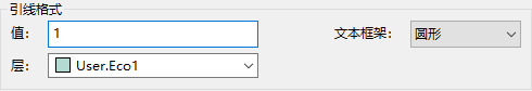
值: 输入要在引线行末尾显示的文本。
文本框架: 选择所需的文本周围的边界(圆形、矩形或无)。
布线
KiCad 具有交互式布线器的功能:
-
允许对单轨和差分对进行手动或拖动 (半自动) 布线。
-
可通过以下方式修改现有设计:
-
拖动现有布线时重新布线现有布线
-
拖动封装时重新布线连接到封装焊盘的布线
-
-
允许通过插入蛇形线 + 来调整布线长度和差分对的偏移(相位) 为具有严格时序要求的设计调整布线形状
默认情况下,布线器在放置布线时尊重配置的设计规则:新布线的尺寸(宽度)将取自设计规则,在确定新布线和过孔的放置位置时,布线器将尊重设计规则中设置的铜间隙。 如果需要的话,可以通过使用高亮冲突布线器模式和打开布线器设置中的允许 DRC 违规选项来禁用这种行为(见下文)。
布线器有三种模式,可以随时选择。 布线器模式用于布线新布线,但也用于使用拖动(热键 D)命令拖动现有布线时。 这些模式是:
-
高亮冲突:在此模式下,大部分布线器功能被关闭,布线完全手动。 布线时,冲突 (间隙违规) 将以绿色高亮,如果存在冲突,则新布线的布线无法修复,除非打开了允许 DRC 冲突选项。 在此模式下,一次最多可以放置两个布线段 (例如,一个水平线段和一个对角线段)。
-
推挤:在此模式下,被布线的线段将绕过无法移动的障碍物 (例如,焊盘和锁定的布线/孔孔)和 推挤 障碍,这些障碍物可以移开。布线器在此模式下防止违反 DRC:如果无法布线到不违反 DRC 的光标位置,则不会创建新的布线。
-
绕走:在此模式下,布线器的行为与推挤模式相同,只是不会移动障碍物。
使用哪种模式是一个偏好问题。 对于大多数用户,我们建议使用推挤模式以获得最高效的布线体验,或者,如果您不希望布线器修改未被布线的线段,则建议使用绕走模式。请注意,推挤和绕走模式始终创建水平、垂直和 45 度 (H/V/45) 布线段。如果需要使用 H/V/45 以外的角度布线段,则必须使用高亮碰撞模式,并在交互布线器设置对话框中启用自由角度模式选项。
有五个主要的布线功能。单轨布线、差分对布线、调整单轨长度、调整差分对的长度和调整差分对的偏移 (相位)。 所有这些都存在于顶部工具栏上的路由菜单下拉菜单(单独)和绘图工具栏上的两个重载图标中,在右侧的绘图工具栏上。 上面介绍了重载图标的使用。 一个用于两个布线功能,一个用于三个调谐功能。 此外,布线菜单允许选择设置层对和交互式布线器设置。
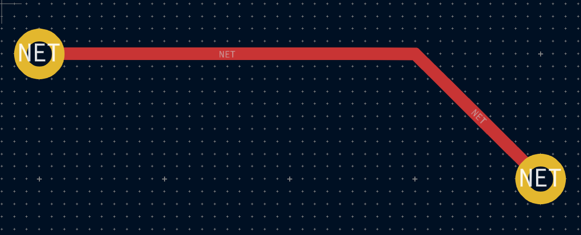
要布线,请点击布线 ![]() 图标(从绘图工具栏或从顶部工具栏 布线 下)或使用热键 X。 点击一个起始位置,选择要布线的网络,并开始布线。 被布线的网络会自动高亮显示,网络的允许间隙会在被布线的线端周围用灰色的轮廓表示。 可以通过改变 "偏好设置" 对话框中的 "间隙轮廓" 设置来禁用间隙轮廓。
图标(从绘图工具栏或从顶部工具栏 布线 下)或使用热键 X。 点击一个起始位置,选择要布线的网络,并开始布线。 被布线的网络会自动高亮显示,网络的允许间隙会在被布线的线端周围用灰色的轮廓表示。 可以通过改变 "偏好设置" 对话框中的 "间隙轮廓" 设置来禁用间隙轮廓。
| 间隙轮廓显示从布线网络到 PCB 上任何其他铜线的最大间隙。 可以使用自定义设计规则为不同对象指定网络的不同间隙。 布线器将考虑这些间隙,但仅直观地显示最大间距值。 |
当布线器处于活动状态时,将从布线起点到编辑器光标绘制新的线段。这些线段是未固定临时 (unfixed temporary) 对象,它们显示当您使用左击或 Enter 键来固定布线 (fix the route) 时将创建哪些线段。非固定布线段以比固定布线段更亮的颜色显示。当您使用 Esc 键或通过选择另一个工具退出布线器时,将只保存固定布线段。完成布线操作(热键 End) 将固定所有布线并退出布线器。
在布线时,可以使用撤消最后一个布线段命令 (热键 Backspace) 取消固定最近固定的布线。您可以重复使用此命令以后退已固定的布线。
在以前的 KiCad 版本中,使用鼠标左键或 Enter 来固定已布线的线段会固定所有线段,但不包括鼠标光标位置结束的线段。 在 KiCad 6 中,这种行为现在是可选的,默认情况下,所有的线段 包括 在鼠标光标位置结束的线段都会被固定。 通过在交互式布线器设置对话框中禁用 "点击后固定所有线段" 选项,可以恢复旧的行为。
布线时,可以按住 Ctrl 键禁用网格捕捉,按住 Shift 键禁用对焊盘和过孔等对象的捕捉。
| 也可以通过更改首选项对话框的编辑选项部分中的磁吸点首选项来禁用对对象的捕捉。 我们建议您在一般情况下保持启用对象捕捉,这样就不会意外地在焊盘或过孔上略微偏离中心结束布线。 |
布线形态
在垂直(H) / 水平 (V) / 45 度模式下布线时,形态 是指一组两个线段如何连接单个 H/V/45 度线段无法到达的两个点。 在这种情况下,这些点将由一条水平或垂直线段和一条对角线 (45度) 线段连接。形态指的是这些线段的顺序:是水平/垂直线段还是对角线线段在前。

KiCad 的布线器试图根据一系列因素自动选择最佳形态。一般说来,布线器会尝试最大限度地减少路线中的拐角数量,并尽可能避免 "坏" 拐角 (如锐角)。当从焊盘布线或布线到焊盘时,KiCad 将选择将路线与焊盘最长边缘对齐的形态。
在某些情况下,KiCad 无法正确猜测您想要的形态。要在布线时切换布线的形态,请使用切换布线形态命令 (热键 /)。
在没有明显的“最佳”形态的情况下(例如,从过孔开始布线时),KiCad 将使用鼠标光标的移动来选择形态。如果希望布线从直线 (水平或垂直) 线段开始,请在水平或垂直方向上将鼠标从起始位置移开。如果您希望布线以对角线开始,请沿对角线方向移动。一旦光标与布线起始位置相距足够远,形态就会被锁定,并且除非光标回到起始位置,否则不会再更改。可以在交互式布线器设置对话框中禁用从鼠标光标移动检测形态,如下所述。
| 如果使用切换布线形态命令覆盖 KiCad 选择的形态,则在当前布线操作的其余部分中,将禁用从鼠标移动自动检测形体。 |
布线转角模式
当以 H/V/45 模式布线时,KiCad 的布线器可以放置尖角或圆角的布线。要在尖角和圆角之间切换,请使用布线拐角模式命令 (热键 Ctrl+/)。使用圆角布线时,每个布线步骤将放置直线段、单个圆弧或同时放置直线段和圆弧。布线形态决定首先放置圆弧还是直线段。
选择所需布线后,还可以在布线后使用圆角布线命令对布线拐角进行圆角处理。
| 尚不支持使用圆弧拖动布线。当拖动布线或在推挤模式下由布线器移动布线时,圆弧将转换回锐角。 |
布线宽度
被布线的线段的宽度是通过以下三种方式之一来确定的:如果布线的起点是现有线段的终点,并且顶部工具栏上的 ![]() 按钮被启用,宽度将被设置为现有布线的宽度。 否则,如果顶部工具栏中的布线宽度下拉菜单被设置为 "使用网络类宽度",则宽度将取自被布线的网络类(或任何为网络类指定不同宽度的自定义设计规则,例如在凹陷区域内)。 最后,如果布线宽度下拉菜单被设置为电路板设置对话框中配置的预定义布线尺寸之一,则将使用该宽度。
按钮被启用,宽度将被设置为现有布线的宽度。 否则,如果顶部工具栏中的布线宽度下拉菜单被设置为 "使用网络类宽度",则宽度将取自被布线的网络类(或任何为网络类指定不同宽度的自定义设计规则,例如在凹陷区域内)。 最后,如果布线宽度下拉菜单被设置为电路板设置对话框中配置的预定义布线尺寸之一,则将使用该宽度。
| 布线宽度永远不能低于在电路板设置对话框的约束部分中配置的最小布线宽度。如果添加的预定义宽度低于此最小约束,则将使用最小约束值。 |
KiCad 的布线器支持活动路线的单一布线宽度。 换句话说,要在线段中间改变宽度,你必须结束路线,然后从上一条线段的末端重新开始一条新的线段。 要改变活动线段的宽度,可使用热键 W 和 Shift+W,在电路板设置对话框中配置的布线宽度中逐步进行。
放置过孔
在布线线段时,切换层会在当前(未固定)线段的末端插入一个过孔。 一旦你放置了过孔,布线将继续在新层上进行。 有几种方法可以选择一个新层并插入过孔:
-
使用热键选择特定的图层,如 PgUp 选择
F.Cu或 PgDn 选择B.Cu。 -
通过使用 "下一层" 或 "上一层" 热键 (+ 和 -)。
-
通过使用 "放置过孔" 热键 (V),它将切换到活动层对中的下一层。
-
通过使用 "选择图层并通过通孔放置" 操作(热键 <),将打开一个对话框来选择目标层。
过孔的尺寸将从激活的过孔尺寸设置中获取,可通过顶部工具栏的下拉列表或增加过孔尺寸 (') 和减小过孔尺寸 (\) 热键访问。与布线宽度非常相似,当通孔大小设置为"使用网络类尺寸" 时,将使用 "电路板设置" 的 "网络类" 部分中配置的过孔大小 (除非被自定义设计规则覆盖)。
如果在电路板设置对话框的约束条件部分启用了微孔或盲/埋孔,就可以在布线时放置这些过孔。 使用热键 Ctrl+V 来放置微孔,Alt+Shift+V 来放置盲/埋孔。 微孔只能被放置在连接一个外铜层和相邻层的位置。 盲孔/埋孔可以放置在任何一层上。
布线器放置的过孔被认为是已布线线段的一部分。 这意味着过孔网络可以自动更新(就像线段网络一样),例如,当从原理图中更新 PCB 时改变了线段的网络名。 在某些情况下,这可能是不需要的,例如在创建邮戳孔时。 对于特定的过孔,可以通过关闭过孔属性对话框中的 "自动更新过孔网络" 复选框来禁用过孔网络的自动更新。 使用 "添加独立过孔" 工具放置的过孔在创建时禁用这一设置。
差分对布线
KiCad 中的差分对被定义为具有共同的 基数名称 和正负后缀的网路。 KiCad 支持使用 ` 和 `-`,或者 `P` 和 `N` 作为后缀。 例如,`USB 和 USB- 构成一对差分,USB_P 和 USB_N 也是如此。 在第一个例子中,基本名称是 USB,第二个例子中是 USB_。 后缀样式不能混合:网路 USB+ 和 USB_N 不构成差分对。 请确保你在原理图中相应地命名你的差分对网络,以便在 PCB 编辑器中使用差分对布线器。
要对差分对进行布线,请点击布线差分对 ![]() 图标(从绘图工具栏或从顶部工具栏 布线 下)或使用热键 6。 点击一个焊盘、过孔或现有差分对线段的末端,开始布线。 你可以从差分对的正网或负网开始布线。
图标(从绘图工具栏或从顶部工具栏 布线 下)或使用热键 6。 点击一个焊盘、过孔或现有差分对线段的末端,开始布线。 你可以从差分对的正网或负网开始布线。
| 目前不可能在现有差分对布线的中间开始对差分对进行布线。 |
差分对布线器将尝试用设计规则中的间隙布线这对布线(差分对间隙可以在电路板设置对话框的网络类部分中配置,也可以通过使用自定义设计规则来配置)。如果布线的起始或结束位置与配置的间隙不同,布线器将创建一个较短的 "扇出" 部分,以最大限度地缩短差分对未耦合的布线长度。
当交换层或使用放置过孔 (V) 操作时,差分对布线器将创建两个相邻的过孔。这些过孔将被放置在尽可能靠近彼此的位置,同时遵守铜和孔到孔间隙的设计规则。
修改布线
线段被布线后,可以通过移动或拖动来修改它们,或者删除并重新布线。 当选择一个线段时,热键 U 可以用来将选择范围扩大到所有连接的线段。 第一次按下 U 将选择与焊盘或过孔最近的连接点之间的线段。 第二次按 U 将再次扩大选择范围,包括所有层上与所选线段相连的所有线段。 用这种技术选择线段可以用来快速删除整个布线网络。
有两种不同的拖动命令可用于修改布线段。拖动 (45 度模式) 命令热键 D 用于通过布线器拖动布线。如果布线器模式设置为推挤,则使用此命令拖动将推挤附近的布线。如果布线器模式设置为绕走,则使用此命令拖动将绕过障碍物或停在障碍物处。拖动自由角度命令 热键 G 用于将布线段一分为二,并将新角点拖动到任何位置。拖动自由角度的行为类似于高亮碰撞布线器模式:不会避开或推挤障碍物,只会高亮。
| 目前还不能拖动包含圆弧的布线。在某些情况下,尝试拖动这些布线会导致圆弧被删除。可以通过选中特定圆弧并使用拖动命令 (D) 来调整其大小。使用此命令调整圆弧大小时,不执行 DRC 检查。 |
移动命令(热键 M)也可以在线段上使用。 该命令将拾取选定的线段,而忽略任何未被选中的附加线段或过孔。 使用移动命令移动线段时,不会进行 DRC 检查。
在移动封装的同时,可以对附着在封装上的线段进行重新布线。 要做到这一点,在选择了一个封装的情况下使用拖动命令(D)。 任何以封装的一个焊盘为终点的线段都将与封装一起被拖动。 这个功能有一些限制:它只在高亮冲突模式下运行,所以附着在封装上的线段不会绕过障碍物或将附近的线段推开。 此外,只有以封装的焊盘为终点的线段才会被拖动。 仅仅穿过焊盘或在原点以外的焊盘上结束的线段将不会被拖动。
可以使用编辑布线和过孔对话框修改布线的宽度和过孔的大小,而无需重新布线。有关详细信息,请参阅下面关于批量编辑工具的部分。
长度调整
长度调谐工具可用于在布线后为线段添加蛇形调谐形状。 要调整线段的长度,首先要挑选合适的长度调谐工具。 单线调谐工具(图标 ![]() 或热键 7)将添加蛇形图形,使单线的长度达到目标值。 差分对调谐工具(图标
或热键 7)将添加蛇形图形,使单线的长度达到目标值。 差分对调谐工具(图标 ![]() 或热键 8)将为差分对做同样的事情。 差分对偏斜调整工具(图标
或热键 8)将为差分对做同样的事情。 差分对偏斜调整工具(图标 ![]() 或热键 9)将为差分对中较短的成员增加长度,以消除差分对正负两边的偏斜(相位差)。 与 "布线" 图标一样,"调谐" 图标可以在顶部工具栏的 "布线" 菜单下拉框和右侧的绘图工具栏中找到。
或热键 9)将为差分对中较短的成员增加长度,以消除差分对正负两边的偏斜(相位差)。 与 "布线" 图标一样,"调谐" 图标可以在顶部工具栏的 "布线" 菜单下拉框和右侧的绘图工具栏中找到。
要选择长度调整工具的目标长度,请在激活长度调整工具后,从上下文菜单或使用热键 Ctrl+L 打开 "长度调整设置" 对话框:
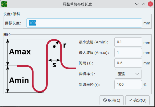
此对话框还可用于配置曲折形状的大小、形状和间距。
配置好目标长度后,在你希望开始放置蛇形形状的区域点击一个布线。 沿着线段移动鼠标光标,蛇形形状就会被添加。 光标旁边会出现一个状态窗口,显示布线的当前长度和目标长度。 再次点击,完成放置当前的蛇形布线。 如果需要,可以在同一条布线上放置多条蛇形布线。
| 长度调整工具仅支持调整两个焊盘之间的点对点网络的长度。尚不支持调整具有不同拓扑的网络长度。 |
交互式布线设置
交互式布线器设置可通过路径菜单访问,或通过右键单击工具栏中的布线按钮来访问。这些设置控制布线和拖动现有布线时的布线行为。
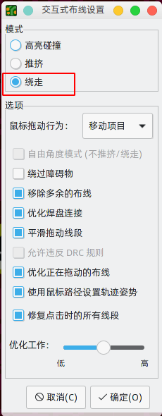
| 设置 | 说明 |
|---|---|
模式 |
设置用于创建新布线和拖动现有布线的路由器的操作模式。 有关详细信息,请参阅上面的内容。 |
自由角度模式 |
允许以任何角度布线,而不是仅以 45 度增量布线。 仅当布线模式设置为突出显示高亮冲突时, 此选项才可用。 |
绕过障碍物 |
在推挤模式下,允许布线尝试在实心障碍物 (如焊盘) 后面移动碰撞布线。 |
移除多余的布线 |
自动删除在当前布线中创建的回路, 仅保留回路中最近布线的部分。 |
优化焊盘连接 |
启用此设置时,交互式布线器尝试在退出焊盘和过孔时避免锐角 和其他不需要的布线。 |
平滑拖动线段 |
拖动布线时,会尝试将布线段组合在一起, 以最大限度地减少方向更改。 |
允许违反 DRC 规则 |
在高亮碰撞模式下,允许放置违反 DRC 规则的布线和过孔。 在其他模式下不起作用。 |
优化正在拖动的布线 |
启用后,拖动布线段将导致 KiCad 优化屏幕上可见的其余布线。 优化过程去除了不必要的拐角,避免了锐角,通常会尝试找到布线的最短路径。 禁用时,不会对正在拖动的紧邻部分之外的布线执行任何优化。 在拖动布线时尝试优化布线。 |
使用鼠标路径设置布线形态 |
尝试根据鼠标路径从布线起点位置拾取布线形态。 如果鼠标从开始位置开始主要沿对角线移动,则形态将设置为对角线起点; 如果鼠标主要水平或垂直移动,则形态将设置为垂直起点。 当鼠标离开布线起始位置很远时,形态估计就会被锁定, 并且可以通过移回起始位置来解锁。 |
点击时固定所有线段 |
启用时,在布线时单击将固定已布线的所有布线段的位置, 包括在鼠标光标结束的线段。新的线段将从鼠标光标位置开始。 禁用时,最后一个线段 (在鼠标光标处结束的线段) 将不会固定在适当位置, 可以通过进一步的鼠标移动进行调整。 |
向前和向后批注
| TODO:写下这一节 |
位置重新批注
| TODO:写下这一节 |
锁定
大多数对象可以通过其属性对话框、右键上下文菜单或使用 "切换锁定" 热键(L)来锁定。 被锁定的对象不能被选择,除非选择过滤器中的 "被锁定的项目" 复选框被启用。 试图移动锁定的项目将导致一个警告对话框:
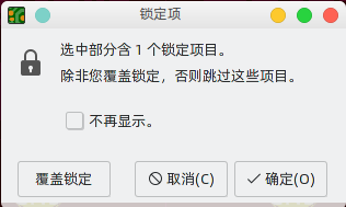
在这个对话框中选择 "覆盖锁定" 将允许移动锁定的项目。 选择 "确定" 将允许你在选择中移动任何未上锁的项目;留下锁定的项目。 选择 "不再显示" 将使你在剩下的会话中记住你的选择。
批量编辑工具
| TODO:写下这一节 |
清理工具
| TODO:写下这一节 |
正在导入图形
| TODO:写下这一节 |
从 DXF 和 SVG 文件导入矢量图
| TODO:写下这一节 |
正在导入位图图像
| TODO:写下这一节 |