Создание печатной платы
Базовые принципы построения печатных плат
Печатная плата в KiCad обычно состоит из посадочных мест,представляющих электронные компоненты и их контактные площадки, цепей для соединения контактных площадок друг с другом, дорожек, переходных отверстий и зон заливки, формирующих соединения между контактными площадками в каждой цепи, а также различные графические формы, определяющие контур платы, обозначения шёлкографии и любую другую необходимую информацию.
Информация о цепях на печатных платах в KiCad обычно синхронизируетсяс соответствующей схемой, но цепи также могу создаваться и редактироваться непосредственно в редакторе печатных плат.
Возможности
KiCad is capable of creating printed circuit boards with up to 32 copper layers, 14 technical layers (silkscreen, solder mask, component adhesive, solder paste, etc), and 13 general-purpose drawing layers.
The internal measurement resolution of all objects in KiCad is 1 nanometer, and measurements are stored as 32-bit integers. This means it is possible to create boards up to approximately 4 meters by 4 meters.
В настоящее время KiCad поддерживает один файл платы на проект / схему.
Создание печатной платы на основе схемы
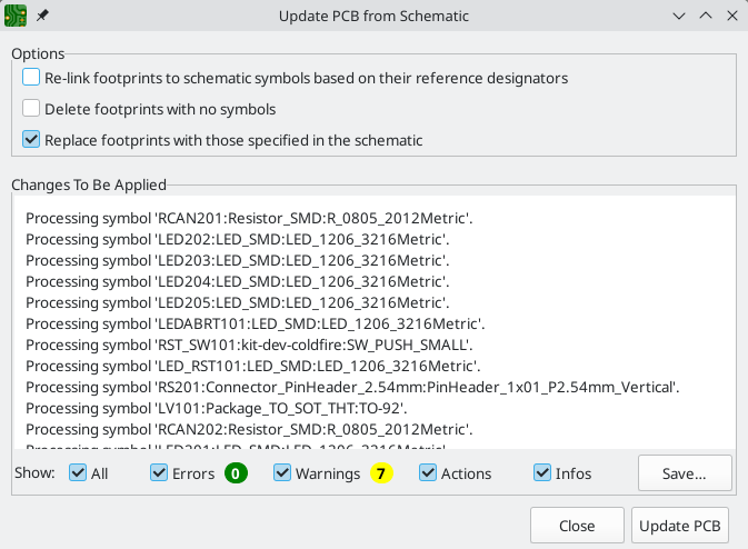
Creating a board from a schematic is the recommended workflow for KiCad. When you create a new project, KiCad will generate an empty board file with the same name as the project. To start designing the board after you have created a schematic, simply open the board file. You can do this either from the KiCad project manager, or by clicking the "Open PCB in board editor" button in the schematic editor. To import the schematic design information into the board editor, including footprints and net connections, use the Tools → Update Schematic from PCB… action (F8). You can also use the ![]() icon in the top toolbar.
icon in the top toolbar.
| Update PCB from Schematic is the preferred way to transfer design information from the schematic to the PCB. In older versions of KiCad, the equivalent process was to export a netlist from the Schematic Editor and import it into the Board Editor. It is no longer necessary to use a netlist file. |
For more information about the Update Schematic from PCB tool, see the forward annotation section of the manual.
Создание платы с нуля
Также можно создать плату без использования схемы, хотя этот рабочий процесс имеет некоторые ограничения и не рекомендован для большинства пользователей. Редактор плат при этом должен быть запущен автономно (не из менеджера проектов KiCad). Перед началом проектирования рекомендуется сохранить файл платы, что приведёт также к созданию файла проекта для сохранения параметров платы. Для выбора места сохранения файла платы выберите пункт «Сохранить как…» из меню «Файл». Файл проекта будет сохранён с тем же именем и в том же месте, которое было выбрано для сохранения файла платы.
Параметры платы
Перед началом проектирования платы, откройте диалоговое окно «Параметры платы» для настройки её основных параметров. Для открытия диалогового окна щёлкните по значку ![]() в верхней панели инструментов или выберите пункт «Параметры платы…» в меню «Файл».
в верхней панели инструментов или выберите пункт «Параметры платы…» в меню «Файл».
Настройка структуры платы и физических параметров
There are two sections of Board Setup used to configure the stackup and layers of the board. The Board Editor Layers section is used to enable or disable technical (non-copper) layers, and give custom names to layers if desired. The Physical Stackup section is used to configure the number of copper layers, as well as the physical parameters of the copper and dielectric layers such as thickness and material type. Dielectric, soldermask, and silkscreen layers can have colors assigned to them, which affects the board’s appearance in the 3D viewer.
Начните настройку параметров структуры платы с раздела «Структура платы»:
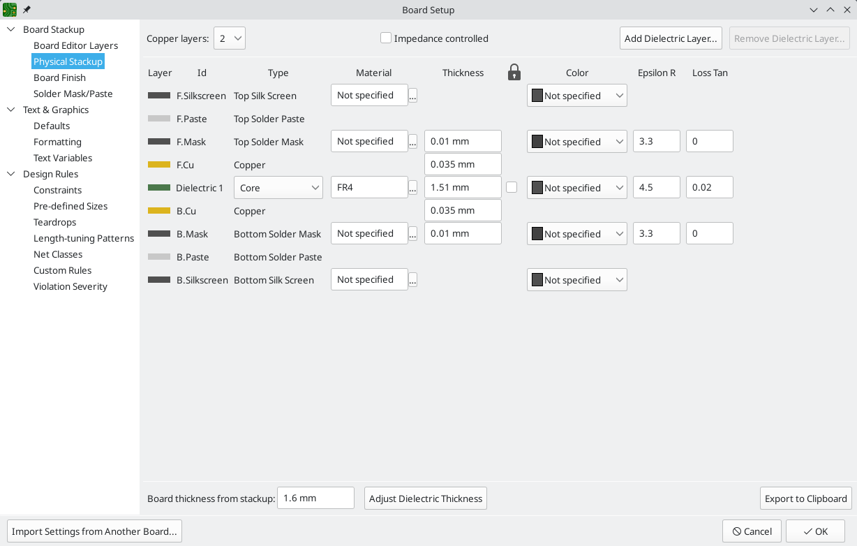
Set the number of copper layers in the upper left corner and then enter the physical parameters of the stackup if desired. These parameters may be left at their default values, but note that the board thickness value will be used when exporting a 3D model of the board, and layer thicknesses will be included in net length calculations for any nets that include vias. If you plan to use these features, it is a good idea to ensure that the stackup thickness is correct.
| KiCad currently only supports stackups with an even number of copper layers. To create designs with an odd number of layers (for example, flexible printed circuits or metal-core printed circuits), simply choose the next highest even number and ignore the extra layer. |
Далее, при необходимости переименуйте слои в разделе «Слои редактора» или скройте не медные слои, которые не будут использоваться при проектировании. Например, если нижняя шёлкография при проектировании использоваться не будет, снимите флажок рядом со слоем B.Silkscreen.
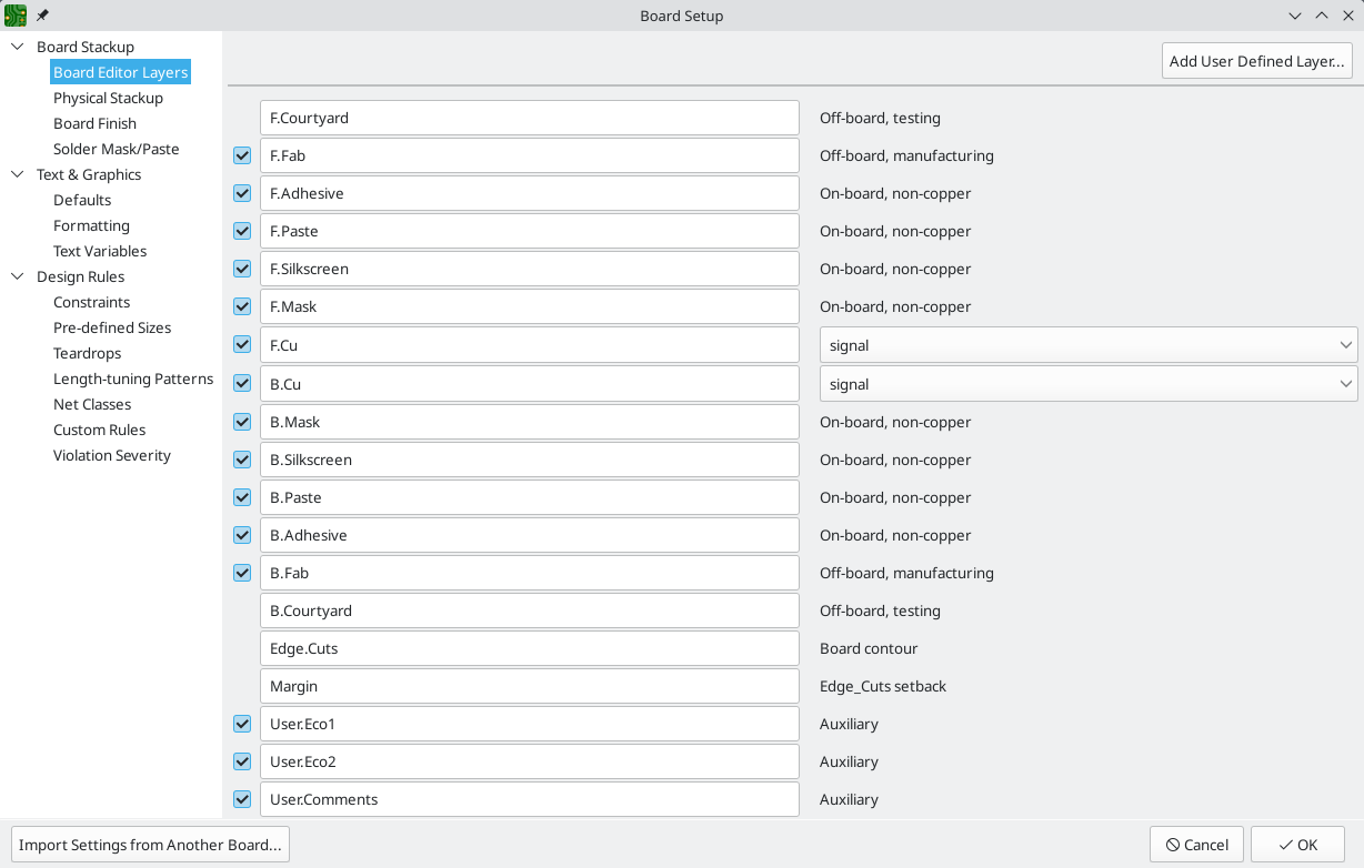
| Copper layers can be designated as signal, power plane, mixed, or jumper in the Board Editor Layers section. This designation is intended as a guide for the user only. Tracks and zones can be routed on any copper layer, no matter what the type is configured to in this dialog. |
Некоторые дополнительные параметры структуры находятся в разделах «Обработка платы» и «Паяльная маска/паста» диалогового окна «Параметры платы». В разделе «Обработка платы» настраиваются параметры, определяющие свойства покрытия меди, а также указываются некоторые конструктивные особенности, такие как создание периферийных полу-отверстий или нанесение покрытия на кромки платы. В настоящее время данные параметры влияют только на вывод атрибутов платы в составе файлов заданий Gerber.
The Solder Mask/Paste section allow global adjustment of the clearance (positive or negative) between the copper shapes and solder mask / solder paste shapes of pads on the board. These values will be added to any clearance overrides set on individual footprints or pads. Positive clearance values will result in the shape of the solder mask or paste opening being larger than the copper shape. Negative clearance values will result in the opening being smaller than the copper shape.
| Most commercial PCB fabricators expect these values to be zero and make their own adjustments to solder mask and paste openings as part of their CAM process. It is usually best to leave these values at their default of zero unless you are making the PCB yourself or have specific advice from your fabricator to use different values. |
Настройка параметров по умолчанию для текста и графики
Раздел параметров по умолчанию для текста и графики в диалоговом окне «Параметры платы» может использоваться для настройки параметров нового текста и графических форм, помещаемых на плату.
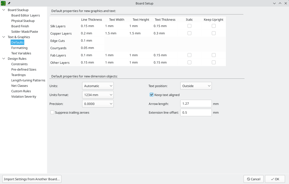
Толщину линии, размер и внешний вид текста можно настроить для различных категорий слоёв, показанных в диалоговом окне. Также для всех слоёв доступна дополнительная настройка параметров размера объектов. Более подробная информация о свойствах размеров представлена в разделе «Размеры» ниже.
Dashed line appearance is controlled in the Formatting section. Dash length controls the length of dashes, while Gap length controls the spacing between dashes and dots. The dash and gap lengths are relative to the line width: a gap length of 2 means twice the width of the line.
Text replacement variables can be created in the Text Variables section. These variables allow you to substitute the variable name for any text string. This substitution happens anywhere the variable name is used inside the variable replacement syntax of ${VARIABLENAME}.
For example, you could create a variable named VERSION and set the text substitution to 1.0. Now, in any text object on the PCB, you can enter ${VERSION} and KiCad will substitute 1.0. If you change the substitution to 2.0, every text object that includes ${VERSION} will be updated automatically. You can also mix regular text and variables. For example, you can create a text object with the text Version: ${VERSION} which will be substituted as Version: 1.0.
Text variables can also be created in Schematic Setup. Text variables are project-wide; variables created in the schematic editor are also available in the board editor, and vice versa.
There are also a number of built-in system text variables.
Настройка правил проектирования
Правила проектирования управляют поведением интерактивного трассировщика, заливкой зон меди и средством проверки правил проектирования. Правила проектирования можно изменять в любой момент времени, но рекомендуется устанавливать все известные правила проектирования в начале процесса проектирования платы.
Ограничения
Basic design rules are configured in the Constraints section of the Board Setup dialog. Constraints in this section apply to the entire board and should be set to the values recommended by your board manufacturer. Any minimum value set here is an absolute minimum and cannot be overridden with a more specific design rule. For example, if you need the copper clearance on part of a board to be 0.2mm and in the rest 0.3mm, you must enter 0.2mm for the minimum copper clearance in the Constraints section and use a netclass or custom rule to set the larger 0.3mm clearance.
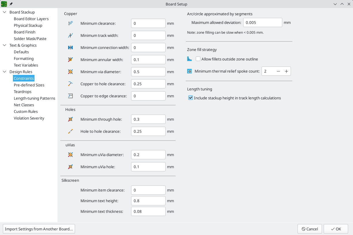
В дополнение к настройками минимального зазора, здесь могут быть заданы и некоторые другие параметры:
| Setting | Description |
|---|---|
Arc/circle approximated by segments |
In some situations, KiCad must use a series of straight line segments to approximate round shapes such as those of arcs and circles. This setting controls the maximum error allowed by this approximation: in other words, the maximum distance between a point on one of these line segments and the true shape of the arc or circle. Setting this to a lower number than the default value of 0.005mm will result in smoother shapes, but can be very slow on larger boards. The default value typically results in arc approximation error that is not detectable in the manufactured board due to manufacturing tolerances. |
Allow fillets outside zone outline |
Zones can have fillets (rounded corners) added in the Zone Properties dialog. By default, no zone copper, including fillets, is allowed outside the zone outline. This effectively means that inside corners of the zone outline will not be filleted even when a fillet is configured. By enabling this setting, inside corners of the zone outline will be filleted even though this results in copper from the zone extending outside the zone outline. |
Minimum thermal relief spoke count |
This sets the minimum acceptable number of thermal relief spokes connecting a pad to a zone. A DRC violation will be generated if this constraint is violated. |
Include stackup height in track length calculations |
By default, the length tuner uses the height of the stackup to calculate the additional length of a track that travels through vias from one layer to another. This calculation relies on the board stackup height being correctly configured. In some situations, it is preferable to ignore the height of vias and just calculate the track length assuming that vias add no length. Disabling this setting will exclude via length from length tuner track length calculations. |
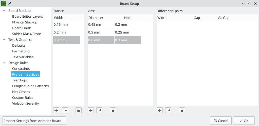
Предустановленные размеры
The pre-defined sizes section allows you to define the track and via dimensions you want to have available while routing tracks. Net classes can be used to define the default dimensions for tracks and vias in different nets (see below) but defining a list of sizes in this section will allow you to step through these sizes while routing. For example, you may want the default track width on a board to be 0.2 mm, but use 0.3 mm for some sections that carry more current, and 0.15 mm for some sections where space is limited. You can define each of these track widths in the Board Setup dialog and then switch between them when routing traces.
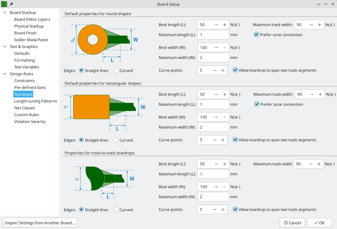
Teardrops
The teardrops section lets you set default parameters for various types of teardrops. There are different settings for teardrop connections to round objects, rectangular objects, and teardrop connections between tracks. The default teardrop parameters can be overridden when teardrops are added, and also changed in the properties for individual connected items. See the teardrops documentation for more information.
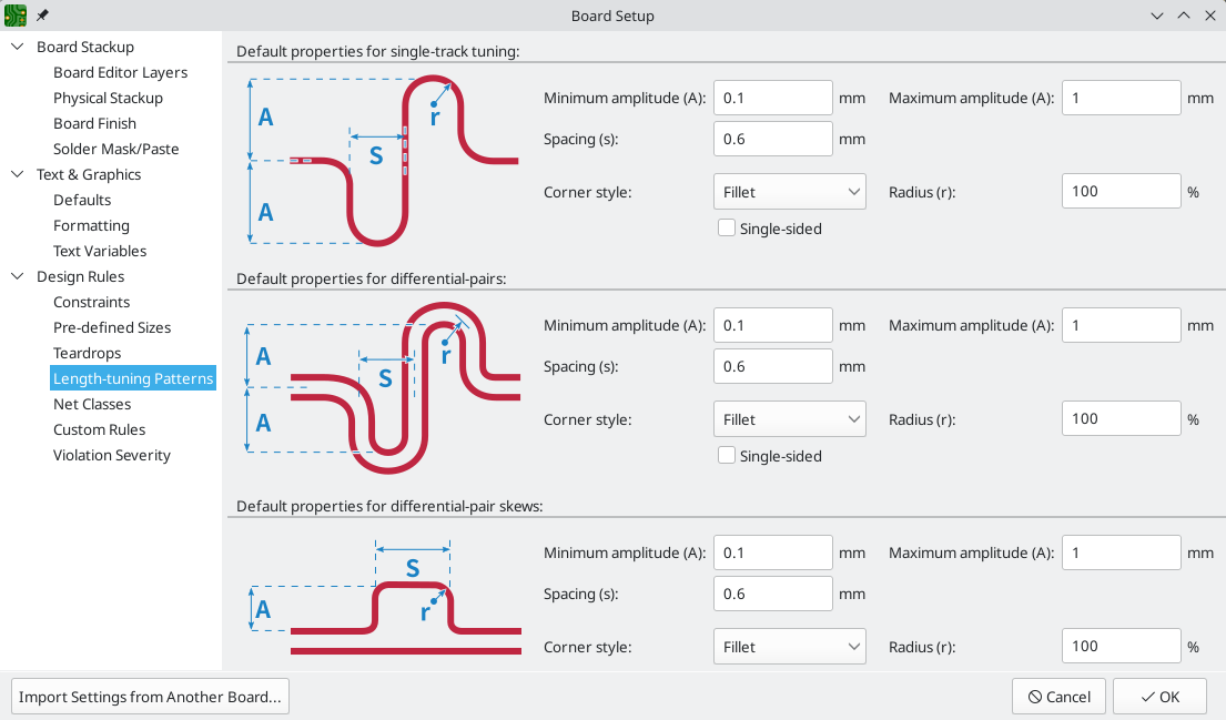
Length-tuning patterns
The length-tuning patterns section lets you set default parameters for each type of length-tuning pattern (single-track length, differential-pair length, and differential-pair skew). These defaults can be overridden in the properties of each tuning pattern added to the board. See the length tuning documentation for more ifnormation.
Классы цепей
The Net Classes section allows you to configure routing and clearance rules for different classes of nets. In KiCad, each net is part of exactly one net class. If you do not add a net to a specific class, it will be part of the Default class, which always exists. Net classes may be created and edited in either the Schematic or Board Setup dialogs.
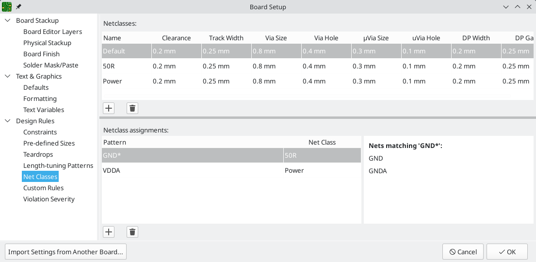
The upper portion of the Net Classes section contains a table showing the net classes in the design and the design rules that apply to each net class. Every class has values for copper clearance, track width, via sizes, and differential pair sizes. These values will be used when creating tracks and vias unless a more specific rule overrides them (see Custom Rules below).
No rule may override the minimum values set in the Constraints section of Board Setup. For
example, if you set a net class clearance to 0.1 mm, but the Minimum Clearance in the
Constraints section is set to 0.2 mm, nets in that class will have a clearance of 0.2 mm.
|
The track widths and via sizes defined for each net class are used when the track width and via size controls are set to "use netclass values" in the PCB editor. These widths and sizes are considered the default, or optimal, sizes for that netclass. They are not minimum or maximum values. Manually changing the track width or via size to a different value from that defined in the Net Classes section will not result in a DRC violation. To restrict track width or via size to specific values, use Custom Rules.
The lower portion of the Net Classes section lists pattern-based netclass assignments. Working with pattern-based netclass assignments is explained in the Schematic Editor documentation; pattern-based assignments can be edited in either the Board or Schematic Setup windows.
Note that pattern-based assignments can be created directly from the PCB editing canvas by right clicking a copper track or zone and clicking Assign netclass…. Netclasses can also be assigned in the schematic using netclass directives or labels instead of pattern-based assignments.
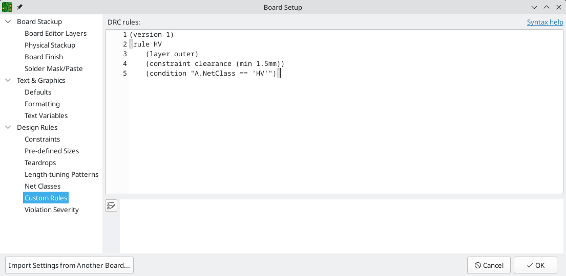
Особые правила
The Custom Rules section contains a text editor for creating design rules using the custom rules language. Custom rules are used to create specific design rule checks that are not covered by the basic constraints or net class settings.
Custom rules will only be applied if there are no errors in the custom rules definitions. Use the Check Rule Syntax button to test the definitions and fix any problems before closing Board Setup.
See Custom Design Rules in the Advanced Topics chapter for more information on the custom rules language as well as example rules.
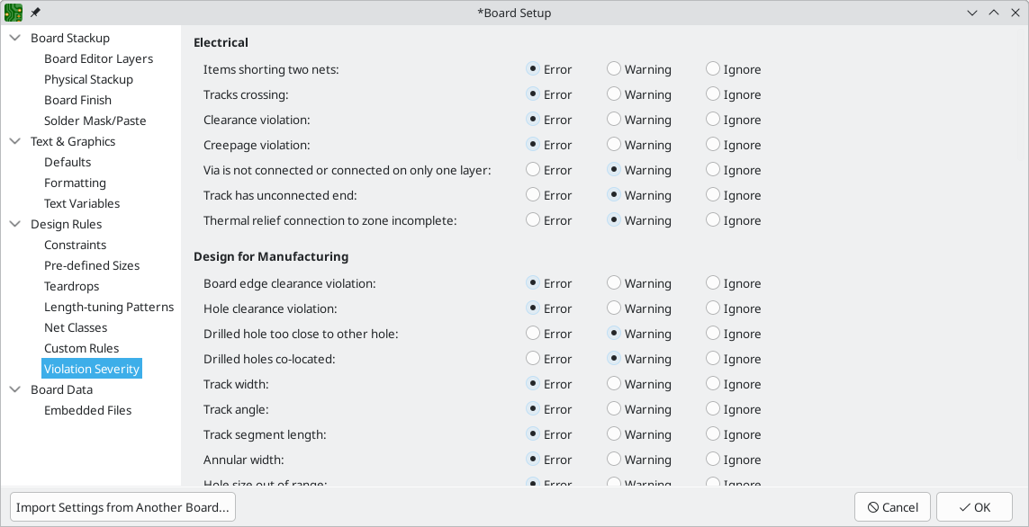
Уровни нарушений
The Violation Severity section allows you to configure the severity of each type of design rule check. Each rule may be set to create an error marker, a warning marker, or no marker (ignored).
| Individual rule violations may be ignored in the Design Rule Checker. Setting a rule to Ignore in the Violation Severity section will completely disable the corresponding design rule check. Use this setting with caution. |
Импорт настроек
Часть или все настройки существующей платы могут быть импортированы. Эту методику можно использовать для создания «шаблона» платы с настройкой параметров, которая будет использоваться в нескольких проектах, чтобы в дальнейшем импортировать эти параметры из шаблона платы в каждую новую плату без необходимости ввода параметров вручную.
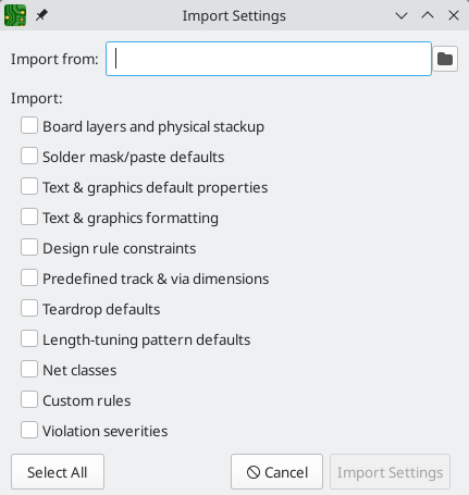
To import settings, click the Import Settings from Another Board… button at the bottom of the Board Setup dialog and then choose the kicad_pcb file you want to import from. Select which settings you want to import and the current settings will be overwritten with the values from the chosen board.