Advanced topics
Configuration and Customization
The KiCad PCB Editor has a variety of preferences that can be configured through the Preferences dialog. Like all parts of KiCad, the preferences for the PCB Editor are stored in the user configuration directory and are independent between KiCad minor versions to allow multiple versions to run side-by-side with independent preferences.
The first sections of the Preferences dialog (Common, Mouse and Touchpad, and Hotkeys) are shared between all KiCad programs. These sections are described in detail in the KiCad manual under the "Common preferences" section.
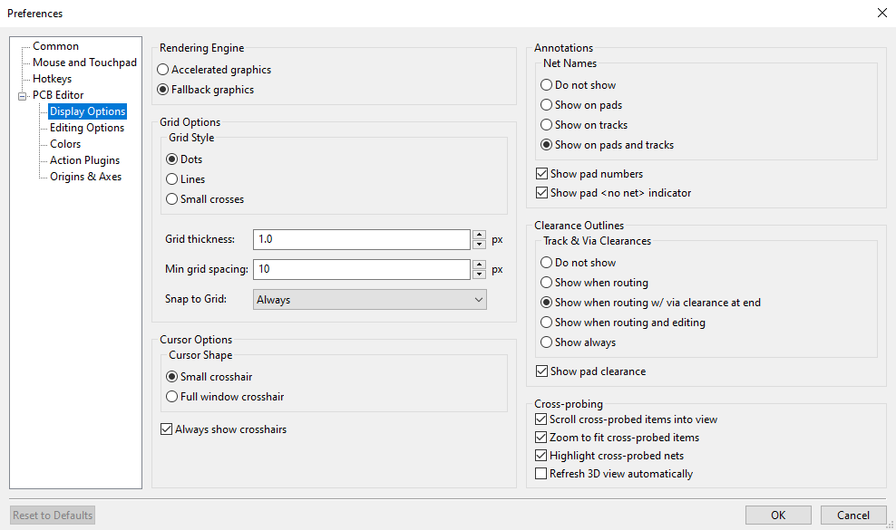
Display options
Rendering Engine: Controls if Accelerated graphics or Fallback graphics are used.
Grid style: Controls how the alignment grid is drawn.
Grid thickness: Controls how thick grid lines or dots are drawn.
Min grid spacing: Controls the minimum distance, in pixels, between two grid lines. Grid lines that violate this minimum spacing will not be drawn, regardless of the current grid setting.
Snap to grid: Controls when drawing and editing operations will be snapped to coordinates on the active grid. "Always" will enable snapping even when the grid is hidden; "When grid shown" will enable snapping only when the grid is visible.
| Grid snapping can be temporarily disabled by holding down Ctrl. |
Cursor shape: Controls whether the editing cursor is drawn as a small crosshair or a full-screen crosshair (a set of lines covering the entire drawing canvas). The editing cursor shows where the next drawing or editing action will occur and will be snapped to a grid location if snapping is enabled.
Always show crosshairs: Controls whether the editing cursor is shown all the time or only when an editing or drawing tool is active.
Net names: Controls whether or not net name labels are drawn on copper objects. These labels are guides for editing only and do not appear in fabrication outputs.
Show pad numbers: Controls whether or not pad number labels are drawn on footprint pads.
Show pad <no net> indicator: Controls whether or not pads with no net are indicated with a special marker.
Track clearance: Controls whether or not clearance outlines around tracks and vias are shown. Clearance outlines are shown as thin shapes around objects that indicate the minimum clearance to other objects, as defined by constraints and design rules.
Show pad clearance: Controls whether or not clearance outlines around pads are shown.
Center view on cross-probed items: When the Schematic and PCB Editors are both running, controls whether clicking a component or pin in Eeschema will center the PCB Editor view on the corresponding footprint or pad.
Zoom to fit cross-probed items: Controls whether the view will be zoomed to show a cross-probed footprint or pad.
Highlight cross-probed nets: Controls whether or not nets highlighted in Eeschema will be highlighted in the PCB Editor when the highlight tool is activated in both tools.
Editing options
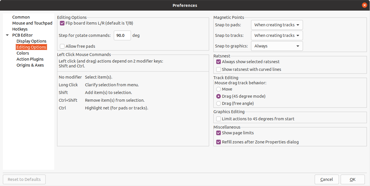
Flip board items L/R: Controls the direction board items will be flipped when moving them between the top and bottom layers. When checked, items are flipped Left-to-Right (about the Vertical axis); when unchecked, items are flipped Top-to-Bottom (about the Horizontal axis).
Step for rotate commands: Controls how far the selected object(s) will be rotated each time the Rotate command is used.
Allow free pads: Controls whether or not the pads of footprints can be unlocked and edited or moved separately from the footprint.
Magnetic points: This section controls object snapping, also called magnetic points. Object snapping takes precedence over grid snapping when it is enabled. Object snapping only works to objects on the active layer. Hold Shift to temporarily disable object snapping.
Snap to pads: Controls when the editing cursor will snap to pad origins.
Snap to tracks: Controls when the editing cursor will snap to track segment endpoints.
Snap to graphics: Controls when the editing cursor will snap to graphic shape points.
Always show selected ratsnest: When enabled, the ratsnest for a selected footprint will always be shown even if the global ratsnest is hidden.
Show ratsnest with curved lines: Controls whether ratsnest lines are drawn straight or curved.
Mouse drag track behavior: Controls the action that will occur when you drag a track segment with the mouse: "Move" will move the track segment independent of any others. "Drag (45 degree mode)" will invoke the push-and-shove router to drag the track, respecting design rules and keeping other track segments attached. "Drag (free angle)" will move the nearest corner of the track segment, highlighting collisions with other objects but not moving them out of the way.
Limit actions to 45 degrees from start Controls whether lines drawn with the graphic drawing tools can take on any angle. Note that this only affects drawing new lines: lines can be edited to take on any angle.
Show page limits: Controls whether or not the page boundary is drawn as a rectangle.
Refill zones after Zone Properties dialog: Controls whether or not zones are automatically refilled after editing the properties of any zone. This may be disabled on complicated designs or slower computers to improve responsiveness.
Colors
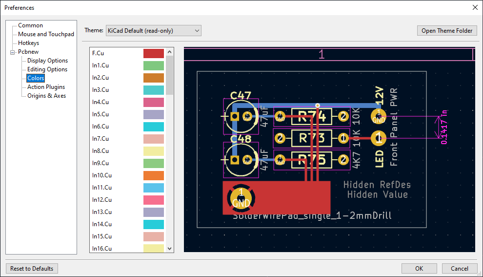
KiCad supports switching between different color themes to match your preferences. Kicad 9.0 comes with two built-in color themes: "KiCad Default" is a new theme designed to have good contrast and balance for most cases and is the default for new installations. "KiCad Classic" is the default theme from KiCad 5.1 and earlier versions. Neither of these built-in themes can be modified, but you can create new themes to customize the look of KiCad as well as install themes made by other users.
Color themes are stored in JSON files located in the colors subdirectory of the KiCad configuration directory. The "Open Theme Folder" button will open this location in your system file manager, making it easy to manage your installed themes. To install a new theme, place it in this folder and restart KiCad. The new theme will be available from the drop-down list of color themes if the file is a valid color theme file.
To create a new color theme, choose New Theme… from the drop-down list of color themes. Enter a name for your theme and then begin editing colors. The colors in the new theme will be copied from whatever theme was selected before you created the new theme.
To change a color, double-click or middle-click the color swatch in the list. The "Reset to Default" button will reset that color to its corresponding entry in the "KiCad Default" color theme.
Color themes are saved automatically; all changes are reflected immediately when you close the Preferences dialog. The window on the right side of the dialog shows a preview of how the selected theme will look.
Action plugins
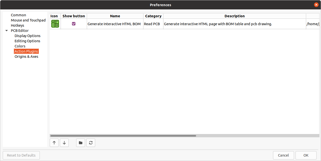
The KiCad PCB editor supports plugins written in Python that can perform actions on the board being edited. These plugins can be installed using the built-in Plugin and Content Manager (see the KiCad chapter for details) or by placing the plugin files inside the user plugins directory. See the Scripting section below for details.
Each plugin that is detected will be shown in a row on this preferences page. Plugins may show a button on the top toolbar of the PCB editor. If the "Show button" control is unchecked for a plugin, it may still be accessed from the Tools > External Plugins menu.
The arrow controls at the bottom of the list allow changing the order that the plugins appear in the toolbar and menu. The folder button will launch a file explorer to the plugin folder, to make installing new plugins easier. The refresh button will scan the plugin folder for any new or removed plugins and update the list.
Origin & axes
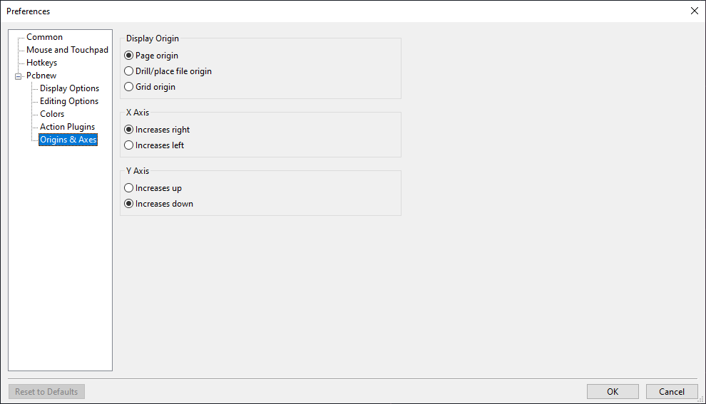
Display origin: Determines which coordinate origin is used for coordinate display in the editing canvas. The page origin is fixed at the corner of the page. The drill/place file origin and the grid origin can be moved by the user.
X axis: Controls whether X-coordinates increase to the right or to the left.
Y axis: Controls whether Y-coordinates increase upwards or downwards.
Text variables
KiCad supports text variables, which allow you to substitute the variable name with a defined text string. This substitution happens anywhere the variable name is used inside the variable replacement syntax of ${VARIABLENAME}.
You can define project text variables in the schematic or board setup dialogs. Project text variables are defined for the whole project, so a project text variable defined in the Schematic Editor can also be used in the Board Editor.
There are also a number of built-in system text variables. System text variables may be available in some contexts and not others. The following variables can be used in PCB text, footprint text, footprint fields, and drawing sheet fields. There are also a number of variables that can be used in the Schematic Editor.
| Variable name | Description |
|---|---|
|
Contents of drawing sheet’s |
|
Contents of drawing sheet’s |
|
Today’s date, in ISO format. |
|
Filename of the board, with a file extension. |
|
Full file path of the board, with a file extension. |
|
Contents of drawing sheet’s |
|
Current version of KiCad. This variable is only available in drawing sheet fields. |
|
Layer of the object. In footprint fields and text objects in footprints, this is
the layer of the field/text object, not the layer of the parent footprint. In
drawing sheet fields, this resolves to the plotted layer, for example |
|
Current sheet’s paper size. This variable is only available in drawing sheet fields. |
|
Project name, without a file extension. |
|
Contents of drawing sheet’s |
|
Contents of drawing sheet’s |
|
Contents of project text variable
|
|
Contents of footprint field Both built-in footprint fields and user-defined fields from the
corresponding symbol are available. Built-in footprint fields use all
uppercase letters: for example, to access a footprint’s value, use
Built-in footprint fields are |
|
Contents of field Both built-in footprint fields and user-defined fields from the
corresponding symbol are available. Built-in footprint fields use all
uppercase letters: for example, to access the value of Built-in footprint fields are |
|
Generates a DRC error named For example, a text item containing |
|
Generates a DRC warning named |
Custom design rules
KiCad’s custom design rule system allows creating design rules that are more specific than the generic rules available in the Constraints page of the Board Setup dialog. Custom design rules have many applications, but in general they are used to apply certain rules to a portion of the board, such as a specific net or net class, a specific area, or a specific footprint.
Custom design rules are stored in a separate file with the extension kicad_dru. This file is created automatically when you start adding custom rules to a project. If you are using custom rules in your project, make sure to save the kicad_dru file along with the kicad_pcb and kicad_pro files when making backups or committing to a version control system.
The kicad_dru file is managed automatically by KiCad and should not be edited with an
external text editor. Always use the Custom Rules page of the Board Setup dialog to edit
custom design rules.
|
The Custom Rules editor
The custom rules editor is located in the Board Setup dialog and provides a text editor for entering custom rules, a syntax checker that will test your custom rules and note any errors, and a syntax help dialog that contains a quick reference to the custom rules language and some example rules.
The custom rules editor also provides context-sensitive autocomplete to suggest valid keywords and properties. The autocomplete suggestion menu appears automatically, but it can also be opened manually by pressing Ctrl+Space.
It is a good idea to use the Check rule syntax button after editing custom rules to make sure there are no syntax errors. Any errors in the custom rules will prevent the design rule checker from running.
Custom rule syntax
The custom design rule language is based on s-expressions and allows you to create design constraints that are not possible with the built-in constraints. Each design rule generally contains a condition defining what objects to match and a constraint defining the rule to be applied to the matched objects.
The language uses parentheses (( and )) to define clauses of related keywords and values. Parentheses must always be matched: for every ( there must be a matching ). Inside a clause, keywords and values are separated by whitespace (spaces, tabs, and newlines). By convention, a single space is used, but any number of whitespace characters between keywords and values is acceptable. In places where text strings are valid, strings without any whitespace may be quoted with " or ', or unquoted. Strings that contain whitespace must always be quoted. Newlines cannot be used within a quoted string. Where nested quotes are required, a single level of nesting is possible by using " for the outer quote character and ' for the inner (or vice versa). Newlines between clauses are not required, but are typically used in examples for clarity.
In the syntax descriptions below, items in <angle brackets> represent keywords or values that must be present and items in [square brackets] represent keywords or values that are optional or only sometimes required.
The Custom Rules file must start with a version header defining the version of the rules language. As of KiCad 9.0, the version is 1. The syntax of the version header is (version <number>). So in KiCad 9.0 the header should read:
(version 1)
After the version header, you can enter any number of rules. Rules are evaluated in reverse order, meaning the last rule in the file is checked first. Once a matching rule is found for a given set objects being tested, no further rules will be checked. In practice, this means that more specific rules should be later in the file, so that they are evaluated before more general rules.
For example, if you create one rule that limits the minimum clearance between tracks in the net HV and tracks in any other net and a second rule that limits the minimum clearance for all objects inside a certain rule area, make sure the first rule appears later in the custom rules file than the second rule. Otherwise tracks in the HV net could have the wrong clearance if they fall inside the rule area.
Each rule must have a name and one or more constraint clauses. The name can be any string and is used to refer to the rule in DRC reports. The constraint defines the behavior of the rule. Rules may also have a condition clause that determines which objects should have the rule applied, an optional layer clause which specifies which board layers the rule applies to, and an optional severity clause which specifies the severity of the resulting DRC violation.
(rule <name>
    [(severity <severity>)]
    [(layer <layer_name>)]
    [(condition <expression>)]
    (constraint <constraint_type> [constraint_arguments]))
The custom rules file may also include comments to describe rules. Comments are denoted by any line that begins with the # character (not including whitespace). You can press Ctrl+/ to comment or uncomment lines automatically.
# Clearance for 400V nets to anything else
(rule HV
    (condition "A.hasNetclass('HV')")
    (constraint clearance (min 1.5mm)))
Custom rules can reference text variables. These are not technically part of the custom rules syntax, but are resolved in a preprocessing step before evaluating the rules file. Because text variables are resolved as a simple text replacement, they can be used anywhere in the DRC rules, as long as all rules are syntactically valid after the variables have been resolved. Text variables could be used, for example, to define a project-wide value that is used in one or more constraints, like (constraint clearance (min ${hv_clearance})), where ${hv_clearance} is a text variable defined in the project as ${3 mm}.
Layer Clause
The layer clause determines which layers the rule will work on. While the layer of objects can be tested in the condition clause as described below, using the layer clause is more efficient.
The value in the layer clause can be any board layer name, or the shortcut keywords outer to match the front and back copper layers (F.Cu and B.Cu) and inner to match any internal copper layers.
If the layer clause is omitted, the rule will apply to all layers.
Some examples:
# Do not allow footprints on back layer (no condition clause means this rule always applies)
(rule "Top side footprints only"
    (layer B.Cu)
    (constraint disallow footprint))

# This rule does the same thing, but is less efficient
(rule "Top side footprints only"
    (condition "A.Layer == 'B.Cu'")
    (constraint disallow footprint))

# Larger clearance on outer layers (inner layer clearance set by board minimum clearance)
(rule "clearance_outer"
    (layer outer)
    (constraint clearance (min 0.25mm)))
Severity Clause
The severity clause sets the DRC violation severity whenever the rule is violated.
Possible values are error, warning, ignore, and exclusion. Ignored rules are not observed by the interactive router and violations are not shown in the DRC dialog. However, ignored rules are evaluated for matching and therefore can still override earlier rules. Errors, warnings, and excluded rules are all observed by the interactive router, and violations are displayed in the DRC dialog when the appropriate filters are selected.
Setting a rule’s severity to ignore does not disable the rule; only the effects of the rule are disabled. The rule is still evaluated and can still override previous rules.
|
Condition Clauses
The condition clause determines which objects which objects the rule applies to. If a rule has a condition clause, the rule will apply to any objects that match the condition. If a rule does not have any condition clauses, it will apply unconditionally.
The rule condition is an expression contained inside a text string (and therefore usually surrounded by quotes in order to allow whitespace for clarity). The expression is evaluated against each pair of objects that is being tested by the design rule checker. For example, when checking for clearance between copper objects, each copper object (track segment, pad, via, etc.) on each net is checked against other copper objects on other nets. If a custom rule exists where the expression matches the two given copper objects and the constraint defines a copper clearance, this custom rule could be used to determine the required clearance between the two objects.
The objects being tested are referred to as A and B in the expression language. The order of the two objects is not important because the design rule checker will test both possible orderings. For example, you can write a rule that assumes that A is a track and B is a via. There are some expression functions that test both objects together; these use AB as the object name.
The expression in a condition must resolve to a boolean value (true or false). If the expression resolves to true, the rule is applied to the given objects.
Each object being tested has properties that can be compared, as well as functions that can be used to perform certain tests. The syntax for using properties and functions is <object>.<property> and <object>.<function>([arguments]) respectively.
When you type <object>. in the text editor (A., B., or AB.), an autocomplete list
will open that contains all the object properties that can be used.
|
The object properties and functions are compared using boolean and relational operators to result in a boolean expression. The following operators are supported:
|
Equal to |
|
Not equal to |
|
Greater than, greater than or equal to |
|
Less than, less than or equal to |
|
And |
|
Or |
|
Not (unary) |
For example, A.NetName == 'VDD' will apply to any objects that are part of the "VDD" net and A.NetName != B.NetName will apply to any objects that have different net names. Parentheses can be used to clarify the order of operations in complex expressions but they are not required. All the boolean operators have the same precedence and are evaluated in order from left to right.
To test a boolean property, evaluate the property itself, without comparing it to a boolean literal like true or false (which don’t exist in the DRC rules language). For example, to test if a footprint’s boolean Do_not_populate property is set, the boolean expression A.Do_not_populate by itself is sufficient. It will resolve to a true value if the footprint’s DNP attribute is set, and a false value otherwise. To check if a boolean is false, use the ! operator (unary not): !A.Do_not_populate will resolve to a true value if the DNP attribute is unset, and a false value otherwise.
Some properties represent a physical measurement, such as a size, angle, length, position, etc. On these properties, unit suffixes can be used in the custom rules language to specify what units are being used. If no unit suffix is used, the internal representation of the property will be used instead (nanometers for distances and degrees for most angles). The following suffixes are supported:
|
Millimeters |
|
Thousandths of an inch (mils) |
|
Inches |
|
Degrees |
|
Radians |
| The units used in custom design rules are independent of the display units in the PCB editor. |
Numeric conditions can use simple math expressions, for example (condition "A.Hole_Size_X == 1.0mm + 0.1mm").
Constraint Clauses
The constraint clause of the rule defines the behavior of the rule on the objects that are matched by the condition. Each constraint clause has a constraint type and one or more arguments that set the behavior of the constraint. A single rule may have multiple constraint clauses, in order to set multiple constraints (for example, clearance and track_width) for objects that match the same rule conditions.
Many constraints take arguments that specify a physical measurement or quantity. These constraints support minimum, optimal, and maximum value specification (abbreviated "min/opt/max"). The minimum and maximum values are used for design rule checking: if the actual value is less than the minimum or is greater than the maximum value in the constraint, a DRC error is created. The optimal value is only used for some constraints, and informs KiCad of a "best" value to use by default. For example, the optimal diff_pair_gap is used by the router when placing new differential pairs. No errors will be created if the differential pair is later modified such that the gap between the pair is different from the optimal value, as long as the gap is between the minimum and maximum values (if these are specified). In all cases where a min/opt/max value is accepted, any or all of the minimum, optimal, and maximum value can be specified.
Min/opt/max values are specified as (min <value>), (opt <value>), and (max <value>). For example, a track width constraint may be written as (constraint track_width (min 0.5mm) (opt 0.5mm) (max 1.0mm)) or simply (constraint track_width (min 0.5mm)) if only the minimum width is to be constrained.
Numeric constraint values can use simple math expressions, for example (constraint clearance (min 0.5mm + 0.1mm)).
| Constraint type | Argument type | Description |
|---|---|---|
|
min/opt/max |
Checks the width of annular rings on vias and pads. |
|
boolean expression |
Checks that the boolean expression is true. If the expression is false, a DRC error will be created. The expression can use any of the properties listed in the Object Properties section. |
|
min |
Specifies the electrical clearance between copper objects of different nets. (See
To allow copper objects to overlap (collide), create a |
|
min |
Specifies the creepage between copper objects of different nets. |
|
min |
Checks the width of connections between pads and zones. An error will be generated for each pad
connection that is narrower than the |
|
min |
Checks the clearance between footprint courtyards and generates an error if any two courtyards
are closer than the To allow courtyard objects to overlap (collide), create a |
|
min/opt/max |
Sets the gap between parallel tracks in a differential pair. The |
|
max |
Checks the distance that a differential pair track is routed uncoupled from the other polarity
track in the pair (for example, where the pair fans out from a component, or becomes uncoupled
to pass around another object such as a via). An error will be generated for each differential
pair with an uncoupled distance that is greater than the |
|
|
Specify one or more object types to disallow, separated by spaces. For example,
|
|
min/opt/max |
Checks the clearance between objects and the board edge. This can also be thought of as the "milling tolerance" as the board edge will include all
graphical items on the To allow objects to overlap (collide) with the board edge, create an |
|
min |
Checks the clearance between a drilled hole in a pad or via and copper objects on a different net. The clearance is measured from the diameter of the hole, not its center. |
|
min/max |
Checks the size (diameter) of a drilled hole in a pad or via. For oval holes, the smaller
(minor) diameter will be tested against the |
|
min |
Checks the clearance between mechanically-drilled holes in pads and vias. The clearance is measured between the diameters of the holes, not between their centers. This constraint is solely for the protection of drill bits. The clearance between laser-drilled (microvias) and other non-mechanically-drilled holes is not checked, nor is the clearance between milled (oval-shaped) and other non-mechanically-drilled holes. |
|
min/max |
Checks the total routed length for the nets that match the rule condition and generates an
error for each net that is below the |
|
|
Checks the total number of connections (spokes) to a pad. An error will be raised for each pad that has fewer than the specified number of spokes. |
|
min |
Checks the clearance between two objects, regardless of their nets. This includes objects
with the same net and objects on non-copper layers. Only objects on physical layers and
courtyard layers are checked: this means copper, adhesive, paste, silkscreen, mask,
courtyard, and edge cut layers. Physical clearance is only checked between objects on the
same layer, except for objects on While this can perform more general-purpose checks than |
|
min |
Checks the clearance between a drilled hole in a pad or via and another object, regardless of net. The clearance is measured from the diameter of the hole, not its center. This can also be thought of as the "drilling tolerance" as it only includes round holes
(see |
|
min/opt/max |
Checks the clearance between objects on silkscreen layers and other objects. To allow silkscreen objects to overlap (collide) with other objects, create a |
|
min/opt/max/within_diff_pairs |
Checks the total skew for the nets that match the rule condition, that is, the difference
between the length of each net and the longest net that is matched
by the rule. If the difference between the longest net and the length of any one net is above
the constraint |
|
opt |
Specifies the solder mask expansion for pads, shapes and tracks. |
|
opt |
Specifies the absolute solder paste clearance for pads. Usually negative to inset the paste. The final solder paste clearance will be the absolute clearance plus the relative clearance. |
|
opt |
Specifies the relative solder paste clearance for pads. Usually negative to inset the paste. The final solder paste clearance will be the absolute clearance plus the relative clearance. |
|
min/max |
Checks the height of text, including text boxes. An error will be generated for each text item
that has a height below the |
|
min/max |
Checks the thickness of text, including text boxes. An error will be generated for each text
item that has a thickness below the |
|
min |
Specifies the width of the gap between a pad and a zone with a thermal-relief connection. |
|
opt |
Specifies the width of the spokes connecting a pad to a zone with a thermal-relief connection. |
|
min/max |
Checks the angle between two connected track segments. An error will be generated for each connected pair with an angle below the min value (if specified) or above the max value (if specified). |
|
min/max |
Checks the length of track and arc segments. An error will be generated for each segment that has a width below the min value (if specified) or above the max value (if specified). |
|
min/opt/max |
Checks the width of track and arc segments. An error will be generated for each segment that
has a width below the |
|
min/max |
Counts the number of vias on every net matched by the rule condition. An error will be generated
for each net that has fewer vias than the |
|
Checks for vias that are unconnected or connected on only one layer. This constraint does not take
a min/opt/max value. In combination with a |
|
|
min/max |
Checks the diameter of vias. An error will be generated for each via that has a diameter below
the |
|
|
Specifies the connection to be made between a zone and a pad. |
Object property and function reference
The following properties can be tested in custom rule expressions:
Common Properties
These properties apply to all PCB objects.
| Property | Data type | Description |
|---|---|---|
|
string |
The board layer on which the object exists. For objects that exist on more than one layer,
this property will return the first layer (for example, |
|
boolean |
True if the object is locked. |
|
string |
Returns the unique identifier of the parent object of this object. |
|
dimension |
The position of the object’s origin in the X-axis. Note that the origin of an object is not always the same as the center of the object’s bounding box. For example, the origin of a footprint is the location of the (0, 0) coordinate of that footprint in the footprint editor, but the footprint may have been designed such that this location is not in the center of the courtyard shape. |
|
dimension |
The position of the object’s origin in the Y-axis. Note that KiCad always uses Y-coordinates that increase from the top to bottom of the screen internally, even if you have configured your settings to show the Y-coordinates increasing from bottom to top. |
|
string |
One of "Bitmap", "Dimension", "Footprint", "Graphic", "Group", "Leader", "Pad", "Target", "Text", "Text Box", "Track", "Via", or "Zone". |
Connected Object Properties
These properties apply to copper objects that can have a net assigned (pads, vias, zones, tracks).
| Property | Data type | Description |
|---|---|---|
|
integer |
The net code of the copper object. Note that net codes should not be relied upon to remain
constant: if you need to refer to a specific net in a rule, use |
|
string |
The list of all net classes for the copper object. This is a priority ordered, comma delimited list where a net has multiple net classes assigned. Note that this list may include the In an expression, an object’s
The following expressions are false, however:
You can also check if a copper object is a member of a particular net class,
regardless of any other net classes it may be a part of, using
|
|
string |
The name of the net for the copper object. Note that |
|
boolean |
True if curved edges are enabled for teardrops connected to the object. |
|
boolean |
True if teardrops are enabled for the object. |
|
boolean |
True if the "Prefer zone connections" property is set for the object. |
|
boolean |
True if the "Allow teardrops to span two tracks" property is set for the object. |
|
double |
Best ratio of teardrop length to object size for teardrops connected to the object. |
|
double |
Best ratio of teardrop width to object size for teardrops connected to the object. |
|
dimension |
Maximum length dimension for teardrops connected to the object. |
|
dimension |
Maximum width dimension for teardrops connected to the object. |
|
double |
Maximum allowable ratio of object size to track width for teardrops connected to the object. |
Footprint Properties
These properties apply to footprints.
| Property | Data type | Description |
|---|---|---|
|
dimension |
The copper clearance override set for the footprint. |
|
string |
The name of the component class set for the footprint. This is an alphabetically ordered, comma delimited list where a footprint has multiple component classes assigned. In an expression, a footprint’s
The following expressions are false, however:
Note that while You can also check if an object is part of a footprint with a specific component class using
the |
|
boolean |
True if the footprint’s "Do not populate" attribute is set. |
|
boolean |
True if the footprint’s "Exclude from position files" attribute is set. |
|
boolean |
True if the footprint’s "Exclude from bill of materials" attribute is set. |
|
boolean |
True if the footprint’s "Exempt from courtyard requirement" attribute is set. |
|
string |
The "Keywords" from the library footprint. |
|
string |
The footprint’s description in the footprint library. This is the footprint’s
description property, not the contents of the footprint field named |
|
string |
The link to the library footprint in |
|
boolean |
True if the footprint’s "Not in schematic" attribute is set. |
|
double |
The orientation (rotation) of the footprint in degrees. |
|
string |
The reference designator of the footprint. Note that while footprints have a |
|
dimension |
The solder paste margin override set for the footprint. |
|
dimension |
The solder paste margin ratio override set for the footprint. |
|
dimension |
The thermal relief gap set for the footprint. |
|
dimension |
The thermal relief connection width set for the footprint. |
|
string |
The contents of the "Value" field of the footprint. |
|
string |
One of "Inherited", "None", "Thermal reliefs" or "Solid". |
Pad Properties
These properties apply to footprint pads.
| Property | Data type | Description |
|---|---|---|
|
dimension |
The copper clearance override set for the pad. |
|
string |
One of "None", "BGA pad", "Fiducial, global to board", "Fiducial, local to footprint", "Test point pad", "Heatsink pad", "Castellated pad". |
|
dimension |
The size of the pad’s drilled hole/slot in the X axis. |
|
dimension |
The size of the pad’s drilled hole/slot in the Y axis. |
|
double |
The orientation (rotation) of the pad in degrees. |
|
string |
The "number" of a pad, which can be a string (for example "A1" in a BGA). |
|
string |
One of "Circle", "Rectangle", "Oval", "Trapezoid", "Rounded rectangle", "Chamfered rectangle", or "Custom". |
|
dimension |
The value of the "pad to die length" property of a pad, which is additional length added to the pad’s net when calculating net length. |
|
string |
One of "Through-hole", "SMD", "Edge connector", or "NPTH, mechanical". |
|
string |
The name of the pad (usually the name of the corresponding pin in the schematic). |
|
string |
The electrical type of the pad (usually taken from the corresponding pin in the schematic). One of "Input", "Output", "Bidirectional", "Tri-state", "Passive", "Free", "Unspecified", "Power input", "Power output", "Open collector", "Open emitter", or "Unconnected". Pins with a no-connection flag on them will have a "+no_connect" suffix added to the pin type string. For example, "passive+no_connect" will match a passive pin with a no-connection flag. To match a pin type whether or not the pin has a no-connection flag, use a wildcard: "passive*" will match passive pins with or without a no-connection flag. |
|
double |
For rounded rectangle pads, the ratio of radius to rectangle size. |
|
dimension |
The size of the pad in the X-axis. |
|
dimension |
The size of the pad in the Y-axis. |
|
dimension |
The solder mask margin override set for the pad. |
|
dimension |
The solder paste margin override set for the pad. |
|
dimension |
The solder paste margin ratio override set for the pad. |
|
dimension |
The thermal relief gap set for the pad. |
|
dimension |
The thermal relief connection angle set for the pad. |
|
dimension |
The thermal relief connection width set for the pad. |
|
string |
One of "Inherited", "None", "Thermal reliefs" or "Solid". |
Track and Arc Properties
These properties apply to tracks and arc tracks.
| Property | Data type | Description |
|---|---|---|
|
dimension |
The x-coordinate of the start point. |
|
dimension |
The y-coordinate of the start point. |
|
dimension |
The x-coordinate of the end point. |
|
dimension |
The y-coordinate of the end point. |
|
dimension |
The width of the track or arc. |
Via Properties
These properties apply to vias.
| Property | Data type | Description |
|---|---|---|
|
dimension |
The diameter of the via’s pad. |
|
dimension |
The diameter of the via’s finished hole. |
|
string |
The last layer in the via stackup. |
|
string |
The first layer in the via stackup. |
|
string |
One of "Through", "Blind/buried", or "Micro". |
Tuning Pattern Properties
These properties apply to tuning patterns.
| Property | Data type | Description |
|---|---|---|
|
dimension |
The x-coordinate of the end point. |
|
dimension |
The y-coordinate of the end point. |
|
dimension |
The minimum amplitude of the tuning pattern. |
|
dimension |
The maximum amplitude of the tuning pattern. |
|
string |
One of "Single track", "Differential pair", or "Diff pair skew". |
|
string |
One of "Left", "Right", or "Default". |
|
dimension |
The minimum spacing of the tuning pattern.. |
|
integer |
The corner radius percentage of the tuning pattern. |
|
dimension |
The target length for the tuning pattern. |
|
dimension |
The target skew for the tuning pattern. |
|
boolean |
True if the tuning pattern overrides custom DRC rules. |
|
boolean |
True if the tuning pattern is single-sided. |
|
boolean |
True if the tuning pattern uses rounded meanders. |
Zone and Rule Area Properties
These properties apply to copper and non-copper zones, and rule areas (formerly called keepouts).
| Property | Data type | Description |
|---|---|---|
|
dimension |
The copper clearance override set for the zone. |
|
dimension |
The distance between hatched lines in the zone. |
|
float |
The minimum allowed hatching hole size, expressed as a fraction of the nominal hatching hole size. |
|
integer |
The angle (in degrees) of the hatched lines in the zone. |
|
dimension |
The width of hatched lines in the zone. |
|
dimension |
The minimum allowed width of filled areas in the zone. |
|
string |
The user-specified name (blank by default). |
|
string |
One of "Inherited", "None", "Thermal reliefs", "Solid", or "Thermal Reliefs for PTH". |
|
integer |
The priority level of the zone. |
|
dimension |
The thermal relief gap set for the zone. |
|
dimension |
The thermal relief connection width set for the zone. |
Graphic Shape Properties
These properties apply to graphic lines, arcs, circles, rectangles, and polygons.
| Property | Data type | Description |
|---|---|---|
|
dimension |
The angle of an arc. |
|
dimension |
The x-coordinate of the end point. |
|
dimension |
The y-coordinate of the end point. |
|
boolean |
True if the shape is filled. |
|
dimension |
Thickness of the strokes of the shape. |
|
string |
One of "Solid", "Dashed", "Dotted", "Dash-Dot", "Dash-Dot-Dot". |
|
string |
One of "Segment", "Rectangle", "Arc", "Circle", "Polygon", or "Bezier". |
|
dimension |
The x-coordinate of the start point. |
|
dimension |
The y-coordinate of the start point. |
Text Properties
These properties apply to text objects (footprint fields, free text labels, etc).
| Property | Data type | Description |
|---|---|---|
|
boolean |
True if the text is bold. |
|
dimension |
Height of a character in the font. |
|
string |
Horizontal text justification (alignment): one of "Left", "Center", or "Right". |
|
boolean |
True if the text is italic. |
|
boolean |
True if the text has the knockout property set. |
|
boolean |
True if the text is mirrored. |
|
string |
The name of a footprint field. For text objects that are not footprint fields, this is an empty string. |
|
string |
The contents of the text object. |
|
dimension |
Thickness of the stroke of the font. |
|
dimension |
Width of a character in the font. |
|
string |
Vertical text alignment: one of "Top", "Center", or "Bottom". |
|
boolean |
True if the text object is visible (displayed). |
Expression functions
The following functions can be called on objects in custom rule expressions:
| Function | Objects | Description |
|---|---|---|
|
|
Returns true if all of the object is inside the named rule area or zone. Note that
|
|
|
Returns true if the object exists on the given board layer. |
|
|
Returns true if the object exists on the copper path between the given pads. |
|
|
Returns the value of field |
|
|
Returns true if the set of component classes assigned to the object contains the named component class |
|
|
Returns true if the set of net classes assigned to the object exactly matches the named set of net
classes |
|
|
Returns true if the set of net classes assigned to the object contains the named net class |
|
|
Returns true if the object is part of a differential pair and the base name of the pair
matches the given argument |
|
|
Returns true if any part of the object is inside the named rule area or zone. Rule area and zone names can be set in their respective properties dialogs. If the given area is a filled copper zone, the function tests if the given object is inside any of the filled copper regions of the zone, not if the object is inside the zone’s outline. Deprecated; use |
|
|
Returns true if the any part of the object is inside the courtyard of the given footprint. The
first variant checks both the front or back courtyard and returns true if the object is inside
either one; the second and third variants check a courtyard on a specific layer.
The named footprint
Deprecated; use |
|
|
Returns true if any part of the object is inside the named rule area or zone. Rule area and zone names can be set in their respective properties dialogs. If the given area is a filled copper zone, the function tests if the given object is inside any of the filled copper regions of the zone, not if the object is inside the zone’s outline. |
|
|
Returns true if any part of the object is inside the courtyard of the given footprint. The
first variant checks both the front or back courtyard and returns true if the object is inside
either one; the second and third variants check a courtyard on a specific layer.
The named footprint
|
|
|
Returns true if the object is a blind/buried via. |
|
|
Returns true if the two objects being tested are part of the same differential pair but are
opposite polarities. For example, returns true if |
|
|
Returns true if the object is a microvia. |
|
|
Returns true if the object is a plated hole (in a pad or via). |
|
|
Returns true if the object is a member of the named group Deprecated; use |
|
|
Returns true if the object is a member of a group named |
|
|
Returns true if the object is a member of the given footprint.
The named footprint
|
|
|
Returns true if the object is a member of a schematic sheet named |
|
|
Returns true if the object is a member of a schematic sheet named |
Custom design rule examples
Basic examples
(rule RF_width
    (layer outer)
    (condition "A.hasNetclass('RF')")
    (constraint track_width (min 0.35mm) (max 0.35mm)))

(rule "BGA neckdown"
    (constraint track_width (min 0.2mm) (opt 0.25mm))
    (constraint clearance (min 0.05mm) (opt 0.08mm))
    (condition "A.intersectsCourtyard('U3')"))

# Specify an optimal gap for a particular differential pair
(rule "Clock gap"
    (condition "A.inDiffPair('/CLK')")
    (constraint diff_pair_gap (opt 0.8mm)))

# Specify a larger clearance between differential pairs and anything else
(rule "Differential pair clearance"
    (condition "A.inDiffPair('*') && !AB.isCoupledDiffPair()")
    (constraint clearance (min 1.5mm)))

(rule "copper keepout"
    (constraint disallow track via zone)
    (condition "A.intersectsArea('zone3')"))

(rule "minimum creepage distance for high voltage nets"
    (condition "A.hasNetclass('HV')")
    (constraint creepage (min 5mm)))
Various clearances
(rule "Clearance between Pads of Different Nets"
    (constraint clearance (min 3.0mm))
    (condition "A.Type == 'Pad' && B.Type == 'Pad' && A.Net != B.Net"))

(rule "Pad to Track Clearance"
    (constraint clearance (min 0.2mm))
    (condition "A.Type == 'Pad' && B.Type == 'Track'"))

# Enforce a clearance around pads (and other copper objects) in a specific footprint
(rule "Pad clearance in R1"
    (constraint clearance (min 1mm))
    (condition "A.memberOfFootprint('TP1')"))

# Enforce a mechanical clearance between components and board edge
(rule front_mechanical_board_edge_clearance
    (layer "F.Courtyard")
    (constraint physical_clearance (min 3mm))
    (condition "B.Layer == 'Edge.Cuts'"))

# Prevent copper pours under capacitors
(rule "No copper pours under capacitors"
    (constraint physical_clearance (min 0.1mm))
    (condition "A.Type == 'Zone' && B.Reference == 'C*'")
)

# This assumes that there is a cutout with 1mm thick lines
(rule "Clearance to cutout"
    (constraint edge_clearance (min 0.8mm))
    (condition "A.Layer=='Edge.Cuts' && A.Line_Width == 1.0mm"))

# prevent silk over tented vias
(rule silk_over_via
    (constraint silk_clearance (min 0.2mm))
    (condition "A.Type == '*Text' && B.Type == 'Via'"))

(rule "Allow connector silk to intersect board edge"
    (constraint silk_clearance)
    (severity ignore)
    (condition "A.memberOfFootprint('J*') && B.Layer=='Edge.Cuts'"))

(rule "Distance between Vias of Different Nets"
    (constraint hole_to_hole (min 0.254mm))
    (condition "A.Type == 'Via' && B.Type == 'Via' && A.Net != B.Net"))

(rule "Via Hole to Track Clearance"
    (constraint hole_clearance (min 0.254mm))
    (condition "A.Type == 'Via' && B.Type == 'Track'"))

(rule "Distance between test points"
    (constraint courtyard_clearance (min 1.5mm))
    (condition "A.Reference =='TP*' && B.Reference == 'TP*"))
High-current design rules
# Check current-carrying capacity
(rule high-current
    (constraint track_width (min 1.0mm))
    (constraint connection_width (min 0.8mm))
    (condition "A.hasNetclass('Power')"))

# Don't use thermal reliefs on heatsink pads
(rule heat_sink_pad
    (constraint zone_connection solid)
    (condition "A.Fabrication_Property == 'Heatsink pad'"))

# Require all four thermal relief spokes to connect to parent zone
(rule fully_spoked_pads
    (constraint min_resolved_spokes 4))

# Set thermal relief gap & spoke width for all zones
(rule defined_relief
    (constraint thermal_relief_gap (min 10mil))
    (constraint thermal_spoke_width (min 12mil)))

# Override thermal relief gap & spoke width for GND and PWR zones
(rule defined_relief_pwr
    (constraint thermal_relief_gap (min 10mil))
    (constraint thermal_spoke_width (min 12mil))
    (condition "A.Name == 'zone_GND' || A.Name == 'zone_PWR'"))

# Prevent solder wicking from SMD pads
(rule holes_in_pads
    (constraint physical_hole_clearance (min 0.2mm))
    (condition "B.Pad_Type == 'SMD'"))

# Disallow solder mask margin overrides
(rule "disallow solder mask margin overrides"
    (constraint assertion "A.Soldermask_Margin_Override == 0mm")
    (condition "A.Type == 'Pad'"))
Hole sizes
(rule "Max Drill Hole Size Mechanical"
    (constraint hole_size (max 6.3mm))
    (condition "A.Pad_Type == 'NPTH, mechanical'"))

(rule "Max Drill Hole Size PTH"
    (constraint hole_size (max 6.35mm))
    (condition "A.Pad_Type == 'Through-hole'"))

# Separate drill bit and milling cutter size constraints
(rule "Plated through-hole size"
    (constraint hole_size (min 0.2mm) (max 6.35mm))
    (condition "A.isPlated() && A.Hole_Size_X == A.Hole_Size_Y"))

(rule "Plated slot size"
    (constraint hole_size (min 0.5mm))
    (condition "A.isPlated() && A.Hole_Size_X != A.Hole_Size_Y"))
Mask expansion and paste margin
# No solder mask expansion for vias
(rule "no mask expansion on vias"
    (constraint solder_mask_expansion (opt 0mm))
    (condition "A.type == via"))


# Remove solder paste from DNP footprints
(rule remove_solder_paste_from_DNP
    (constraint solder_paste_abs_margin (opt -50mm))
    (condition "A.Do_not_Populate"))
Dangling vias
# allow dangling vias within a specific rule area named 'dangling vias allowed'
(rule ignore_left
    (constraint via_dangling)
    (condition "A.enclosedByArea('dangling vias allowed')")
    (severity ignore))
Scripting
Scripting allows you to automate tasks within KiCad using the Python language. KiCad provides an API for editing PCBs that can be used interactively or in standalone scripts. Board Editor scripts can be organized as "action plugins", which are displayed as icons in the top toolbar of the Board Editor. There is also a separate Footprint Wizard API that can be used to create footprint creation plugins for the Footprint Editor.
This manual covers general scripting concepts for the Board Editor’s pcbnew API as well as for the footprint wizard API. Users wishing to write or modify scripts should also use the Doxygen documentation for these APIs located at https://docs.kicad.org/doxygen-python-nightly/namespaces.html.
KiCad 6 or newer requires Python 3 for scripting support. Python 2 is no longer supported.
Using the scripting console
The PCB Editor comes with a built-in Python console that can be used to inspect and interact with the board. To launch the console, use the ![]() button in the top toolbar. The PCB Editor Python API is not automatically loaded, so to load it, type
button in the top toolbar. The PCB Editor Python API is not automatically loaded, so to load it, type import pcbnew into the console. The command pcbnew.GetBoard() will then return a reference to the board currently loaded in the PCB Editor, which can be inspected and modified through the console.
Python script locations
Plugin scripts (PCB action plugins and footprint wizards) can be installed automatically using the Plugin and Content Manager (PCM), or manually by copying the plugin to a folder. Manually installed plugins should each be in their own folder within the plugins folder. The location of the plugins folder is by default:
| Platform | Path |
|---|---|
Linx |
|
macOS |
|
Windows |
|
The type of plugin is determined by the Python class it inherits from. Inheriting from
FootprintWizardBase.FootprintWizard will create a footprint wizard plugin, and inheriting from
pcbnew.ActionPlugin will create an action plugin. Creating action plugins and footprint wizards
is described in more detail below.
|
pcbnew API overview
The scripting API reflects the internal object structure inside KiCad’s Board Editor. It is provided by the pcbnew module in Python.
| Because the API is tightly coupled to KiCad’s internals, the API will change over time and is not considered stable. Consult the doxygen documentation for the most up-to-date API reference, and be sure to use the documentation for the appropriate version of KiCad. |
Scripts, action plugins, and interactive scripting sessions often start with a call to GetBoard(), which returns a BOARD object representing the currently open board and its contents.
BOARD has a set of properties and a set for each type of object in the board: footprints, zones, tracks, vias, text, etc. Each type of object has its own properties and holds its own objects: a footprint will likely have at least one pad, for example.
The objects in the BOARD can be accessed using methods that each return an iterable list of the corresponding object type. A selection of these methods are listed below. Other methods are listed in the doxygen documentation.
-
board.GetFootprints(): returns a list of all of the footprints in the board. -
board.GetDrawings(): returns a list of miscellaneous board objects in the board. -
board.GetTracks(): returns a list of all of the tracks and vias in the board. -
board.GetZones(): returns a list of all of the zones in the board. -
board.GetNetClasses():returns a list of all net classes in the board’s design rules.
Boards can be loaded and saved from disk using the following functions:
-
LoadBoard(filename): loads a board from file, returning aBOARDobject, using the file format that matches the filename extension. -
SaveBoard(filename, board): saves aBOARDobject to file, using the file format that matches the filename extension. -
board.Save(filename): the same asSaveBoard(), but a method of theBOARDobject.
その他の例
Load a board, hide all values, and show all references.
#!/usr/bin/env python3
import sys
from pcbnew import LoadBoard

filename = sys.argv[1]

pcb = LoadBoard(filename)
for fp in pcb.GetFootprints():
    print(f"* Footprint: {fp.GetReference()}")
    fp.Value().SetVisible(False)      # set Value as Hidden
    fp.Reference().SetVisible(True)   # set Reference as Visible

pcb.Save("mod_" + filename)
Change the paste mask margin for pins 1-14 of a footprint.
#!/usr/bin/env python3
import sys
from pcbnew import *

filename=sys.argv[1]
pcb = LoadBoard(filename)

# Find module U304
u304 = pcb.FindFootprintByReference('U304')
pads = u304.Pads()

#  Iterate over pads, printing solder paste margin
for p in pads:
    print(p.GetPadName(), ToMM(p.GetLocalSolderPasteMargin()))
    id = int(p.GetPadName())
    # Set margin to 0 for all but pad (pin) 15
    if id<15: p.SetLocalSolderPasteMargin(0)

pcb.Save("mod_"+filename)
Load a footprint library, list footprints in the library, and list pads in each footprint.
#!/usr/bin/env python3
from pcbnew import *

libpath = "/usr/share/kicad/footprints/Connector_PinSocket_2.54mm.pretty"
print(f">> enumerate footprints, pads of {libpath}")

# Load the suitable plugin to read/write the .pretty library
src_type = PCB_IO_MGR.GuessPluginTypeFromLibPath( libpath );
# We can force the plugin type by using IO_MGR.PluginFind( IO_MGR.KICAD )
plugin = PCB_IO_MGR.PluginFind( src_type )

# Print plugin type name: (Expecting "KiCad" for a .pretty library)
print(f"Selected plugin type: {PCB_IO_MGR.ShowType(src_type)}")

list_of_footprints = plugin.FootprintEnumerate(libpath)

for name in list_of_footprints:
    fp = plugin.FootprintLoad(libpath,name)
    # print the short name of the footprint
    print(name)
    # followed by ref field, value field, and decription string:
    # Remember ref and value texts are dummy text, replaced by the schematic values
    # when reading a netlist.
    print(f"  -> {fp.GetReference()} {fp.GetValue()} {fp.GetLibDescription()}")
    for pad in fp.Pads():
        print(
            f"    pad [{pad.GetPadName()}] at "
            f"pos ({ToMM(pad.GetPosition().x)}, {ToMM(pad.GetPosition().y)}) mm,",
            f"shape offset ({ToMM(pad.GetOffset().x)}, {ToMM(pad.GetOffset().y)}) mm"
        )
    print()
Load a board and print information about each item in the board.
#!/usr/bin/env python
import sys
from pcbnew import *

filename=sys.argv[1]
pcb = LoadBoard(filename)

print("Listing Tracks and Vias:")
for item in pcb.GetTracks():
    if type(item) is PCB_VIA:
        pos = item.GetPosition()
        drill = item.GetDrillValue()
        width = item.GetWidth()
        print(f" * Via:   {ToMM(pos)} - {ToMM(drill)}/{ToMM(width)}")
    elif type(item) is PCB_TRACK:
        start = item.GetStart()
        end = item.GetEnd()
        width = item.GetWidth()
        print(f" * Track: {ToMM(start)} to {ToMM(end)}, width {ToMM(width)}")
    else:
        print(f"Unknown type    {type(item)}")

print()
print("Listing Text and Shapes:")
for item in pcb.GetDrawings():
    if type(item) is PCB_TEXT:
        print(f"* Text:    '{item.GetText()}' at {ToMM(item.GetPosition())}")
    elif type(item) is PCB_SHAPE:
        print(f"* Drawing: {item.GetShapeStr()}")
    else:
        print(f"Unknown type    {type(item)}")

print()
print("Listing Footprints")
for fp in pcb.GetFootprints():
    print(f"* Footprint: {fp.GetReference()} at {ToMM(fp.GetPosition())}")

print()
print(f"Ratsnest count: {pcb.GetNetCount()}")
print(f"Track width count: {len(pcb.GetTrackWidthList())}")
print(f"Via size count: {len(pcb.GetViasDimensionsList())}")

print()
print(f"Listing Zones: {pcb.GetAreaCount()}")
for idx in range(0, pcb.GetAreaCount()):
    zone = pcb.GetArea(idx)
    print(f"zone: {idx} priority: {zone.GetAssignedPriority()} netname: {zone.GetNetname()}")

print()
print(f"Netclasses: {len(pcb.GetAllNetClasses())}")
Action plugins
Action plugin associate a script with a button in the PCB Editor GUI. Clicking the button runs the script. Action plugins are shown in the Tools → External plugins menu, and can also be shown in the toolbar if enabled in the Action Plugins page of the Preferences dialog.
The example below is an action plugin that uses KiCad’s pcbnew API to replace the string $date$ with the current date in any text item.
import pcbnew
import re
import datetime

class text_by_date(pcbnew.ActionPlugin):
    """
    test_by_date: A sample plugin as an example of ActionPlugin
    Add the date to any text field of the board containing '$date$'
    How to use:
    - Add a text on your board with the content '$date$'
    - Call the plugin
    - The text will automatically be updated with the date (format YYYY-MM-DD)
    """

    def defaults(self):
        """
        Method defaults must be redefined
        self.name should be the menu label to use
        self.category should be the category (not yet used)
        self.description should be a comprehensive description
          of the plugin
        """
        self.name = "Add date on PCB"
        self.category = "Modify PCB"
        self.description = "Automatically add date on an existing PCB"

    def Run(self):
        pcb = pcbnew.GetBoard()
        for item in pcb.GetDrawings():
            if item.GetClass() == "PCB_TEXT":
                txt = re.sub("\$date\$ [0-9]{4}-[0-9]{2}-[0-9]{2}",
                                 "$date$", item.GetText())
                if txt == "$date$":
                    item.SetText("$date$ %s" % datetime.date.today())


text_by_date().register()
Footprint wizards
Footprint wizards are Python scripts that can be accessed from the Footprint Editor. Each footprint wizard presents a selection of parameters defined in the Python script, and creates a footprint based on the parameter values.
There are 3 minimum steps required to create a footprint wizard, which are described below. For examples of how to create footprint wizards, see the footprint wizards included with KiCad.
-
Instantiate a Python class, inheriting from
FootprintWizardBase.FootprintWizard. -
Define the 6 required functions:
GetName(),GetDescription(),GetValue(),GenerateParameterList(),CheckParameters(), andBuildThisFootprint(). -
Register the class by calling
{your_class_name}().register().
The GetName(), GetDescription(), and GetValue() functions are there to provide strings to the UI. The only functionality needed is to return an appropriate string.
The GenerateParameterList() function defines the parameters needed for the footprint. Parameters are grouped into a page + name format. For example, calling self.AddParam("demo", "radius", self.uMM, 5) would add a parameter named radius into the page named demo. Retrieving that parameter data would be done with a call such as self.footprint_radius = self.parameters["demo"]["radius"].
The CheckParameters() function is available to perform any data validation on the parameters defined in GenerateParameterList(). This function is also where the self.footprint_radius = self.parameters["demo"]["radius"] calls reside.
The BuildThisFootprint() function is where the footprint building steps are called. This function is where one creates the footprint.
The required {your_class_name}().register() call can either be at the end of the Python file, or in an __init__.py file. Both styles are supported by KiCad.
KiCad will not reload a plugin after it has raised an error (for example, the NotImplementedError).
One will need completely close out KiCad and restart it. However, this doesn’t apply to changes
which do not raise an error.
|
IDF component outlines
KiCad can export an IDF representation of the board for use in mechanical CAD software. Below is some guidance on attaching IDF component outlines to footprints, creating new IDF component outlines, and a description of the IDF utilities included with KiCad.
IDF Exporter で使用するコンポーネントモデルの指定
IDF component models are attached to footprints using the footprint’s 3D model properties. The IDF exporter uses different filetypes than the 3D viewer and other 3D model exporters, so adding 3D models for the IDF exporter does not conflict with 3D models added to a footprint for other purposes.
To add an IDF model to a footprint in the footprint or PCB editors, edit the footprint’s properties and click on the 3D Models tab.
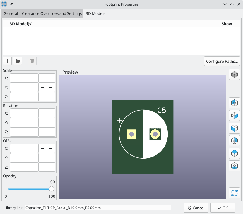
Click the ![]() button and select the IDF (*.idf;*.IDF) filetype filter. Browse to the desired outline file.
button and select the IDF (*.idf;*.IDF) filetype filter. Browse to the desired outline file.
Once the desired component outline file is selected, enter any necessary values for the offset and rotation. The offsets must be specified using the IDF board output units (mm or mils) and in the IDF coordinate system, which is a right-hand coordinate system with +Z pointing towards the viewer, +X to the viewer’s right, and +Y towards the upper edge of the screen. The rotation must be in degrees; positive rotation is a counter-clockwise rotation as described in the IDFv3 specification.
Multiple outlines may be combined with appropriate offsets to represent simple assemblies such as a DIP package in a socket.
| Only the offset values and the Z rotation value are used by the IDF exporter; all other values are ignored. |
コンポーネント・アウトライン・ファイルの生成
The component outline file (*.idf) consists of a single .ELECTRICAL or .MECHANICAL section as described in the specification document. The section may be preceded by any number of comment lines; the comment lines are copied by the exporter into the library file and can be used to track metadata such as references to the documents used to determine the component’s outline and dimensions.
コンポーネント・アウトラインのセクションは、複数の文字列、整数、浮動小数点数のフィールドを含みます。一つの文字列は複数の文字(空白を含む)の組み合わせから成ります。;もし文字列が空白を含む場合は引用符で囲まなければなりません。引用符を文字列の中に入れることはできません。浮動小数点数は十進記数法または指数表記で表すことができますが、可読性から十進記数法を使うことが好ましいでしょう。小数点はカンマ(,)ではなく、ドット(.)でなければなりません。IDF ファイルは 7-bit アスキー文字のみで構成しなければなりません。;8-bit 文字を使用した場合の挙動は不定となります。
An IDF file consists of SECTIONS which consist of RECORDS which consist of FIELDS. For the IDF outline files only one type of section may exist and must be one of .ELECTRICAL or .MECHANICAL. A record is a single line of text and may contain one or more fields. Fields are sequences of characters separated by one or more spaces which do not appear between quotation marks. All fields of a record must appear on a single line; records may not span lines.
The section heading (.ELECTRICAL or .MECHANICAL) is considered the first record (Record 1) of the section. Record 1 must be followed by Record 2 which has four fields:
-
ジオメトリ名: 部品番号と結合した文字列はコンポーネント・アウトラインを表す固有識別子となるべきです。標準化されたパッケージでは、ジオメトリ名としてパッケージ名が適切です。(例“SOT-23”)カスタム品のパッケージには、製造業者の品番がジオメトリ名として良い選択となります。
-
部品番号: 明らかに部品番号を意図したもの(例 BS107)だとしても、この文字列をパッケージを表すために使ったほうが良いでしょう。例えば、ジオメトリ名が“TO-92”なら、部品番号の記載はパッドのレイアウトや他のTO-92と異なる向きを示すために使えるかも知れません。
-
IDF Unit: this must be one of
MMorTHOUand it applies only to the units describing this single component outline. -
高さ: Field 3 で指定された単位を用いた、コンポーネントの図面上の高さを表す浮動小数点数です。
Record 2 には、コンポーネントのアウトラインを指定する Record 3 が続かなければなりません。Record 3 は4つのフィールドからなります。
-
Loop Index:
0(outline points are specified in counter-clockwise order) or1(outline points are specified in clockwise order) -
X 座標: 浮動小数点数です。
-
Y 座標: 浮動小数点数です。
-
Included Angle: a floating point number. If the value is
0then a straight line segment is drawn from the previous point to this point. If the value is360then the previous point specifies the center of a circle and this point specifies a point on the circle; never specify a circle using a value of-360as at least one major mechanical CAD package does not behave well in that situation. If the value is negative then a clockwise arc is drawn from the previous point to this point and if the value is positive then a counter-clockwise arc is drawn.
ただ一つの閉じたループのみが許容され、切削部を指定することはできません。アウトラインが円である場合を除き、最後の点は最初の点と等しくなければなりません。
例 IDF ファイル 1:
# a simple cylinder - this could represent an electrolytic capacitor
.ELECTRICAL
    "cylinder" "5mm OD, 5mm height" MM 5
    0 0 0 0
    0 2.5 0 360
.END_ELECTRICAL
例 IDF ファイル 2:
# an upside-down T
# a comment added for the sake of adding comments
.ELECTRICAL
    "Capital T" "5x8x10mm, upside down" MM 10
    0 -0.5 8 0
    0 -0.5 0.5 0
    0 -2.5 0.5 0
    0 -2.5 -0.5 180
    0 2.5 -0.5 0
    0 2.5 0.5 180
    0 0.5 0.5 0
    0 0.5 8 0
    0 -0.5 8 180
.END_ELECTRICAL
アウトライン作成のためのガイドライン
アウトラインを作成するとき(特に複数で作業するような場合)、ファイルの名前と設計における一貫性は、素早くファイルを見つけたり、最少の努力で部品を配置するために役立ちます。
パッケージの命名
ユーザーがアウトラインの概要を把握できるよう、ファイル名にアウトラインについての情報を付加するように努めるべきです。例えば、円筒形のアキシャルリード・パッケージは抵抗だけではなくコンデンサにも使われるので、アキシャルリード部品のアウトラインが横向きなのか若しくは縦向きなのかを識別することは意味があります。また関連する寸法についていくつかの情報(: 直径、長さ、ピッチ)を付加することは最も重要です。もし部品がカスタム品で特別なアウトラインを持つような場合、製造業者の品番や種類を表すプレフィックスを使うことが適切です。
Comments
ユーザーにアウトラインについての関連情報(例えば、寸法情報の出典に関する参照事項)を提供するためは IDF ファイル内でコメントを使用します。
ジオメトリと部品番号の入力
ジオメトリと部品番号へ入力する値は慎重に考慮しましょう。まとめて扱うべきです。これらの文字列は機械系CADに対して固有識別子として働きます。文字列の値はユーザーにとって意味があることが理想的ですが、必須ではありません。: 値は主として機械系CADで固有識別子として使用するためのものです。理想的には、選ばれた値はいかなる多くのアウトラインに対しても固有のものとなるでしょう。; 十分に選ばれた値は、特に複数の基板においても衝突を少なく抑えることにつながります。
ピンの向きと配置
Component outlines should be created to match the orientation and position of the corresponding footprints. This avoids the need to specify a non-zero rotation for the IDF component outline. Since the IDF exporter ignores the (X, Y) offset values, it is vital that you use the correct origin in the IDF component outline.
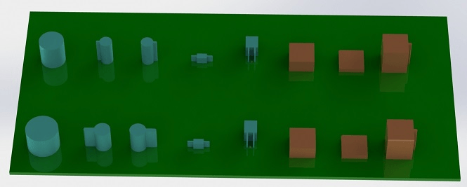
The image above shows sample outlines generated by the programs idfcyl and idfrect and rendered in a mechanical CAD program. From left to right are (a) vertical radial leaded cylinder, (b) vertical axial leaded cylinder with wire on left, (c) vertical axial leaded cylinder with wire on right, (d) horizontal axial leaded cylinder, (e) horizontal radial leaded cylinder, (f) square outline, plain, (g) square outline with chamfer, (h) square outline with axial lead on right. The top outlines were specified in units of millimeters while the bottom outlines were specified in units of inches.
寸法についてのTips
突き出たアウトラインを使う目的は、機構設計者に各部品が占有する物理的な空間とその位置を認識させることです。典型的なシナリオでは、機構設計者はより詳細な機械的モデルを持つ幾つかの加工していないアウトラインと入れ替えるでしょう。例えば直角に実装された LED がパネルの穴に確実に合うか確認する場合です。多くの場合、アウトラインの正確さは重要ではありませんが、可能な限り正確な機械的情報が伝わるようなアウトラインを作ることは良い慣行です。少ない例ですが、例えば携帯型音楽プレーヤーのように、ユーザーが余分の空間が殆どないケースへコンポーネントを収めることを望むこともあるでしょう。このような場合、最も突き出たアウトラインがコンポーネントの表現として十分ならば、機構設計者はケースを設計する時にほんの少数のモデルと入れ替えるだけで済むでしょう。もしアウトラインが実際の大きさを反映していると信頼できないなら、機構設計者は確実にケースに収めるため(機械的)モデルを置き換えることに多くの時間を取られるでしょう。結局のところ、あなたがゴミを入れたなら、出てくるものはゴミしか期待できません。もしあなたが適切な情報を与えたなら、良い結果を確信できます。
IDF コンポーネント・アウトライン・ツール
いくつかのコマンドラインツールが IDF コンポーネント・アウトラインの生成を助けます。ツールは次のものとなります:
-
idfcyl:creates an outline of a cylinder in vertical or horizontal orientation and with axial or radial leads -
idfrect:creates an outline of a rectangle which may have either an axial lead or a chamfer in the top left corner -
dxf2idf:converts a drawing in DXF format into an IDF component outline
idfcyl
idfcyl generates outlines for cylindrical components.
When idfcyl is invoked with no arguments it prints out a usage note and a summary of its inputs:
idfcyl: このプログラムは円筒形コンポーネントのアウトラインを作成します。
 円筒は横向き又は縦向きです。
 横向き円筒は片側または両側に配線できます。
 縦向き円筒は左または右側のどちらかに配線できます。

Input:
    単位: mm, in (mm または inch)
    向き: V (縦向き)
    リードの種類: X, R (アキシャル, ラジアル)
    本体の直径
    本体の長さ
    基板のオフセット
    *   配線の直径
    *   ピッチ
    **  配線面: L, R (左, 右)
    *** リードの長さ
    ファイル名 (*.idf で終わらなければならない)

    NOTES:
        *   横向き又は縦向きアキシャルリード
            でのみ必要です

        **  縦向きのアキシャルリードでのみ必要です

        *** 横向きのラジアルリードでのみ必要です
NOTES はコマンドラインに任意の引数を入力することで非表示にできます。ユーザーはコマンドラインで情報を手入力するか、アウトラインを生成するスクリプトを作ることができます。次のスクリプトは右手側にリードを持った単独のアキシャルリード・アウトラインを作成します。:
#!/bin/bash
# Generate a cylindrical IDF outline for test purposes
# vertical 5mm cylinder,  nominal length 8mm + 3mm board offset,
# axial wire on right,  0.8mm wire dia., 3.5mm pitch
idfcyl - 1 > /dev/null <<  _EOF
mm
v
x
5
8
3
0.8
3.5
r
cylvmm_1R_D5_L8_Z3_WD0.8_P3.5.idf
_EOF
idfrect
idfrect generates outlines for rectangular components.
When idfrect is invoked with no arguments it prints out a usage note and a summary of its inputs:
idfrect: このプログラムは矩形コンポーネントのアウトラインを作成します。
    コンポーネントは一つのリード (アキシャル) または面取りされた
    左上のコーナーを持ちます。
Input:
    単位: mm, in (mm または inch)
    幅
    長さ
    高さ
    面取り: 45度面取りの長さ
    *  リード: Y,N (リードは常に右)
    ** 配線の直径
    ** ピッチ
    ファイル名 (*.idf で終わらなければならない)

    NOTES:
        *   面取り = 0 の場合に必要

        **  リードコンポーネントでのみ必要
NOTES はコマンドラインに任意の引数を入力することで非表示にできます。ユーザーはコマンドラインで情報を手入力するか、アウトラインを生成するスクリプトを作ることができます。次のスクリプトは面取りされた矩形とアキシャルリードのアウトラインを作成します。:
#!/bin/bash
# Generate various rectangular IDF outlines for test purposes
# 10x10, 1mm chamfer, 2mm height
idfrect - 1 > /dev/null <<  _EOF
mm
10
10
2
1
rectMM_10x10x2_C0.5.idf
_EOF
# 10x10x12,  0.8mm lead on 6mm pitch
idfrect - 1 > /dev/null <<  _EOF
mm
10
10
12
0
Y
0.8
6
rectLMM_10x10x12_D0.8_P6.0.idf
_EOF
dxf2idf
dxf2idf creates an IDF component file from a DXF outline.
The DXF file used to specify the component outline can be prepared with the free software LibreCAD for best compatibility.
When dxf2idf is invoked with no arguments it prints out a usage note and a summary of its inputs:
dxf2idf: このプログラムは DXF ファイルから線、弧、円のセグメントを取り出し、
    IDF コンポーネント・アウトライン・ファイルを作成します。

Input:
    DXF ファイル名: 入力ファイル, '.dxf' で終わらなければならない
    単位: mm, in (mm または inch)
    ジオメトリ名: 文字列, IDF version 3.0 仕様に準拠
    パート番号: パート番号の IDF version 3.0 仕様に準拠
    高さ: アウトラインの突き出た部分の高さ
    コメント: 空ではない全ての行は IDF ファイルへ
        追加されたコメントです
        空行はコメントブロックの終わりを示します
    ファイル名 (*.idf で終わらなければならない)
The notes can be suppressed by entering any arbitrary argument on the command line. A user can manually enter information at the command line or create scripts to generate outlines. The following script creates a 5mm high outline from a DXF file test.dxf:
#!/bin/bash
# Generate an IDF outlines from a DXF file
dxf2idf - 1 > /dev/null << _EOF
test.dxf
mm
DXF TEST GEOMETRY
DXF TEST PART
5
This is an IDF test file produced from the outline 'test.dxf'
This is a second IDF comment to demonstrate multiple comments

test_dxf2idf.idf
_EOF
idf2vrml
The idf2vrml tool reads a set of one IDF Board (.emn) and one IDF Component file (.emp) and produces a VRML file which can be viewed with a VRML viewer. This feature is useful for visualization of the board assembly in cases where the user does not have access to MCAD software. Invoking idf2vrml without any arguments will result in the display of a usage message:
>./idf2vrml
Usage: idf2vrml -f input_file.emn -s scale_factor {-k} {-d} {-z} {-m}
flags:
   -k: produce KiCad-friendly VRML output; default is compact VRML
   -d: suppress substitution of default outlines
   -z: suppress rendering of zero-height outlines
   -m: print object mapping to stdout for debugging purposes
example to produce a model for use by KiCad: idf2vrml -f input.emn -s 0.3937008 -k
The idf2vrml tool does not correctly render OTHER_OUTLINE entities in an emn file if that entity is specified on the back layer of the PCB; however you will not noticeable using files exported by KiCad because there is no mechanism to specify such an entity. This is only an issue if you render a third party emn file which does employ an entity on the back side of a board.
|