Creating a PCB
Basic PCB concepts
A printed circuit board in KiCad is generally made up of footprints representing electronic components and their pads, nets defining how those pads connect to each other, tracks, vias, and filled zones that form the copper connections between pads in each net, and various graphic shapes defining the board edge, silkscreen markings, and any other desired information.
KiCad normally keeps the information about nets on a PCB synchronized with an associated schematic, but nets can also be created and edited directly within the PCB editor.
Capabilities
KiCad is capable of creating printed circuit boards with up to 32 copper layers, 14 technical layers (silkscreen, solder mask, component adhesive, solder paste, etc), and 13 general-purpose drawing layers.
The internal measurement resolution of all objects in KiCad is 1 nanometer, and measurements are stored as 32-bit integers. This means it is possible to create boards up to approximately 4 meters by 4 meters.
KiCad currently supports one board file per project / schematic.
Starting from a schematic
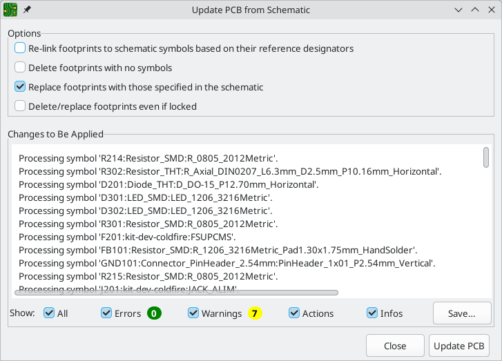
Creating a board from a schematic is the recommended workflow for KiCad. When you create a new
project, KiCad will generate an empty board file with the same name as the project. To start
designing the board after you have created a schematic, simply open the board file. You can do
this either from the KiCad project manager, or by clicking the "Open PCB in board editor" button in
the schematic editor. To import the schematic design information into the board editor, including
footprints and net connections, use the Tools → Update PCB from Schematic… action
(F8). You can also use the
![]() icon in the top toolbar.
icon in the top toolbar.
| Update PCB from Schematic is the preferred way to transfer design information from the schematic to the PCB. In older versions of KiCad, the equivalent process was to export a netlist from the Schematic Editor and import it into the Board Editor. It is no longer necessary to use a netlist file. |
For more information about the Update Schematic from PCB tool, see the forward annotation section of the manual.
Starting from scratch
It is also possible to create a board with no matching schematic, although this workflow has some limitations and is not recommended for most users. To do this, you must start the PCB editor standalone (not from the KiCad project manager). Before beginning your design, it is a good idea to save the board file, which will also create a project file to store board settings. Use "Save As…" from the File menu to choose where to save your board file. A project file with the same name will be created in the same location you choose to save the board file in.
Board setup
Before beginning your board design, use the Board Setup dialog to configure the basic parameters of
the board. To open Board Setup, click the ![]() icon in the top
toolbar or choose "Board Setup…" from the File menu.
icon in the top
toolbar or choose "Board Setup…" from the File menu.
Configuring board stackup and physical parameters
There are two sections of Board Setup used to configure the stackup and layers of the board. The Board Editor Layers section is used to enable or disable technical (non-copper) layers, and give custom names to layers if desired. The Physical Stackup section is used to configure the number of copper layers, as well as the physical parameters of the copper and dielectric layers such as thickness and material type. Dielectric, soldermask, and silkscreen layers can have colors assigned to them, which affects the board’s appearance in the 3D viewer.
To configure the board stackup, start on the Physical Stackup section:
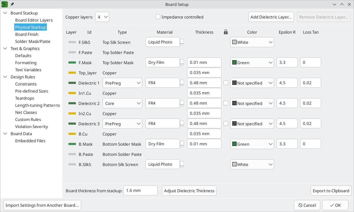
Set the number of copper layers in the upper left corner and then enter the physical parameters of the stackup if desired. These parameters may be left at their default values, but note that the board thickness value will be used when exporting a 3D model of the board, and layer thicknesses will be included in net length calculations for any nets that include vias. If you plan to use these features, it is a good idea to ensure that the stackup thickness is correct.
| KiCad currently only supports stackups with an even number of copper layers. To create designs with an odd number of layers (for example, flexible printed circuits or metal-core printed circuits), simply choose the next highest even number and ignore the extra layer. |
Next, if desired, use the Board Editor Layers section to rename layers or hide non-copper layers
that you will not be using in the design. For example, if you will not use a back silkscreen on
the design, uncheck the box next to the B.Silkscreen layer. Some layers, like F.Cu / B.Cu or
Edge.Cuts, are required layers and therefore cannot be disabled.
| Copper layers can be designated as signal, power plane, mixed, or jumper in the Board Editor Layers section. This designation is intended as a guide for the user only. Tracks and zones can be routed on any copper layer, no matter what the type is configured to in this dialog. |
You can add additional user-defined layers (User.1, User.2, etc.) by clicking the
Add User Defined Layer… button in the top right. User-defined layers can’t be used for routing,
but they can contain arbitrary graphics or other information. By default, user layers are auxiliary
layers, meaning that whatever information they contain does not correspond to either the front or back
of the board. User layers can instead be set to Off-board, front or Off-board, back, in which
case they correspond to the selected side of the board. Items on such layers can be flipped from front
to back in the same way as objects on physical front/back layers. Adjacent front/back layers are treated
as paired: if User.2 is defined as a front layer and User.3 is defined as a back layer, flipping an
object on User.2 will move it to User.3, and vice versa.
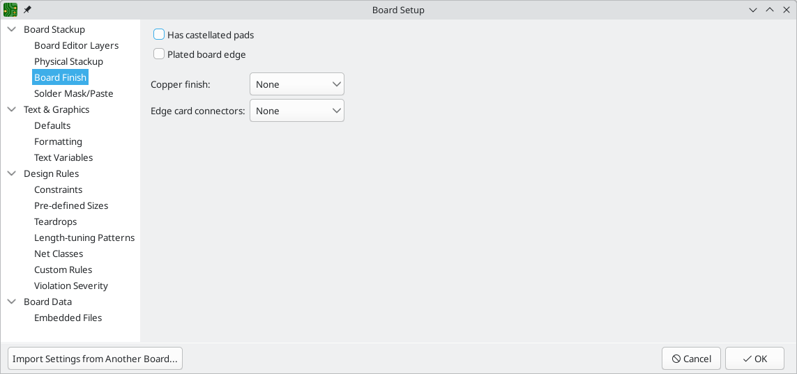
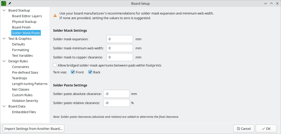
Some additional board stackup settings are found on the Board Finish and Solder Mask/Paste sections of the Board Setup dialog. The Board Finish section has settings for defining the copper finish and special features such as castellations or edge plating. Note that these settings only impact the board attributes output as part of Gerber job files at this time.
The Solder Mask/Paste section allow global adjustment of the clearance (positive or negative) between the copper shapes and solder mask / solder paste shapes of pads on the board. These values will be added to any clearance overrides set on individual footprints or pads. Positive clearance values will result in the shape of the solder mask or paste opening being larger than the copper shape. Negative clearance values will result in the opening being smaller than the copper shape.
| Most commercial PCB fabricators expect these values to be zero and make their own adjustments to solder mask and paste openings as part of their CAM process. It is usually best to leave these values at their default of zero unless you are making the PCB yourself or have specific advice from your fabricator to use different values. |
Configuring default text and graphic settings
The Text & Graphics Defaults section of the Board Setup dialog can be used to configure the properties that will be used for new text and graphic shapes that are placed on the board.
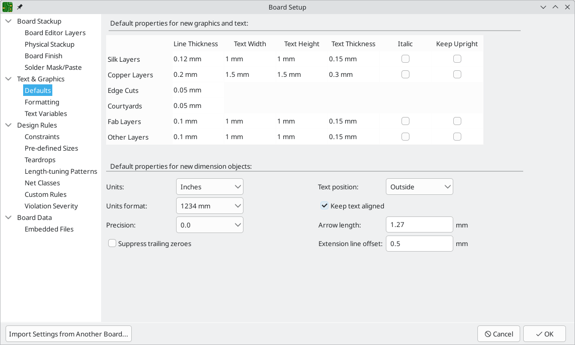
Line thickness, text size, and text appearance can be configured for the six different categories of layers shown in the dialog. Additionally, the properties for dimension objects can be configured for all layers. For more details about dimension properties, see the Dimensions section below.
Dashed line appearance is controlled in the Formatting section. Dash length
controls the length of dashes, while Gap length controls the spacing between
dashes and dots. The dash and gap lengths are relative to the line width: a gap
length of 2 means twice the width of the line.
Text replacement variables can be created in the Text Variables section. These variables allow
you to substitute the variable name for any text string. This substitution happens anywhere the
variable name is used inside the variable replacement syntax of ${VARIABLENAME}.
For example, you could create a variable named VERSION and set the text substitution to 1.0.
Now, in any text object on the PCB, you can enter ${VERSION} and KiCad will substitute 1.0. If
you change the substitution to 2.0, every text object that includes ${VERSION} will be updated
automatically. You can also mix regular text and variables. For example, you can create a text
object with the text Version: ${VERSION} which will be substituted as Version: 1.0.
Text variables can also be created in Schematic Setup. Text variables are project-wide; variables created in the schematic editor are also available in the board editor, and vice versa.
There are also a number of built-in system text variables.
Configuring design rules
Design rules control the behavior of the interactive router, the filling of copper zones, and the design rule checker. Design rules can be modified at any time, but we recommend that you establish all known design rules at the beginning of the board design process.
Constraints
Basic design rules are configured in the Constraints section of the Board Setup dialog. Constraints in this section apply to the entire board and should be set to the values recommended by your board manufacturer. Any minimum value set here is an absolute minimum and cannot be overridden with a more specific design rule. For example, if you need the copper clearance on part of a board to be 0.2mm and in the rest 0.3mm, you must enter 0.2mm for the minimum copper clearance in the Constraints section and use a net class or custom rule to set the larger 0.3mm clearance.
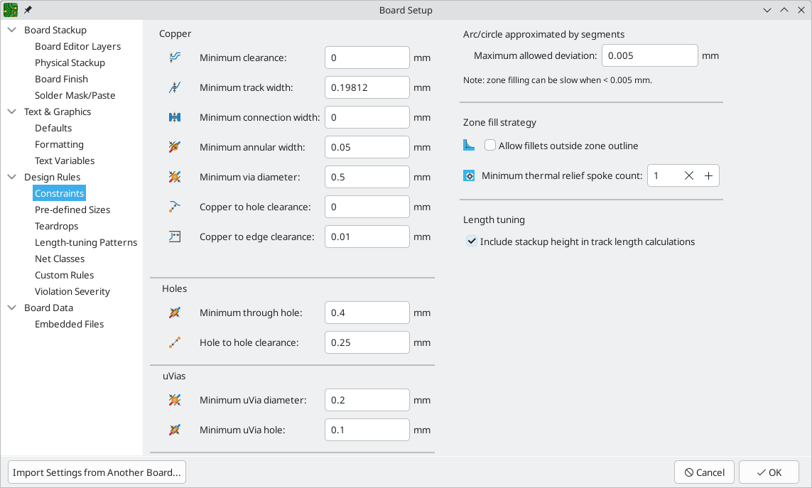
In addition to setting minimum clearances, a number of features can be configured here:
| Setting | Description |
|---|---|
Arc/circle approximated by segments |
In some situations, KiCad must use a series of straight line segments to approximate round shapes such as those of arcs and circles. This setting controls the maximum error allowed by this approximation: in other words, the maximum distance between a point on one of these line segments and the true shape of the arc or circle. Setting this to a lower number than the default value of 0.005mm will result in smoother shapes, but can be very slow on larger boards. The default value typically results in arc approximation error that is not detectable in the manufactured board due to manufacturing tolerances. |
Allow fillets outside zone outline |
Zones can have fillets (rounded corners) added in the Zone Properties dialog. By default, no zone copper, including fillets, is allowed outside the zone outline. This effectively means that inside corners of the zone outline will not be filleted even when a fillet is configured. By enabling this setting, inside corners of the zone outline will be filleted even though this results in copper from the zone extending outside the zone outline. |
Minimum thermal relief spoke count |
This sets the minimum acceptable number of thermal relief spokes connecting a pad to a zone. A DRC violation will be generated if this constraint is violated. |
Include stackup height in track length calculations |
By default, the length tuner uses the height of the stackup to calculate the additional length of a track that travels through vias from one layer to another. This calculation relies on the board stackup height being correctly configured. In some situations, it is preferable to ignore the height of vias and just calculate the track length assuming that vias add no length. Disabling this setting will exclude via length from length tuner track length calculations. |
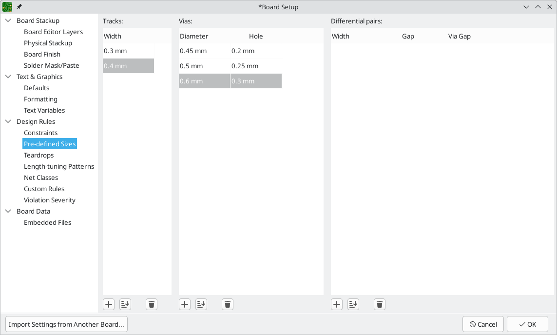
Pre-defined Sizes
The pre-defined sizes section allows you to define the track and via dimensions you want to have available while routing tracks. Net classes can be used to define the default dimensions for tracks and vias in different nets (see below) but defining a list of sizes in this section will allow you to step through these sizes while routing. For example, you may want the default track width on a board to be 0.2 mm, but use 0.3 mm for some sections that carry more current, and 0.15 mm for some sections where space is limited. You can define each of these track widths in the Board Setup dialog and then switch between them when routing tracks.
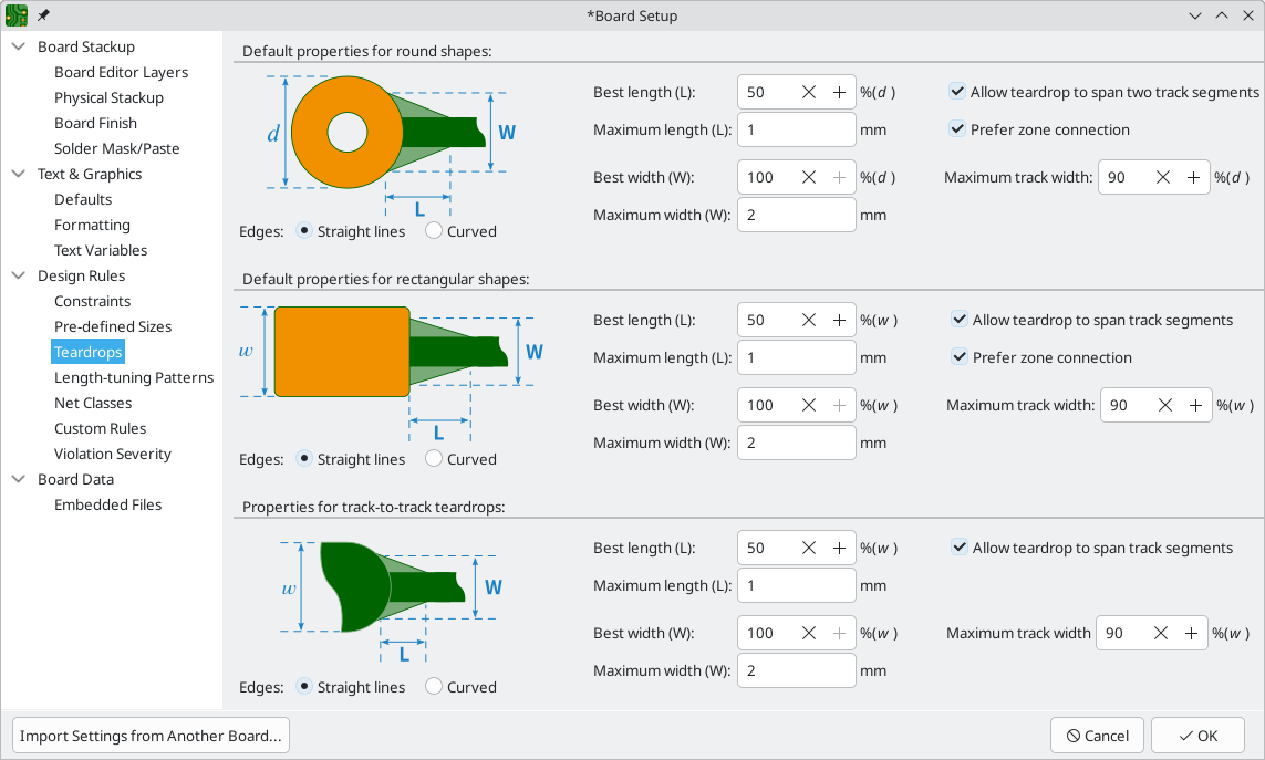
Teardrops
The teardrops section lets you set default parameters for various types of teardrops. There are different settings for teardrop connections to round objects, rectangular objects, and teardrop connections between tracks. The default teardrop parameters can be overridden when teardrops are added, and also changed in the properties for individual connected items. See the teardrops documentation for more information about each setting.
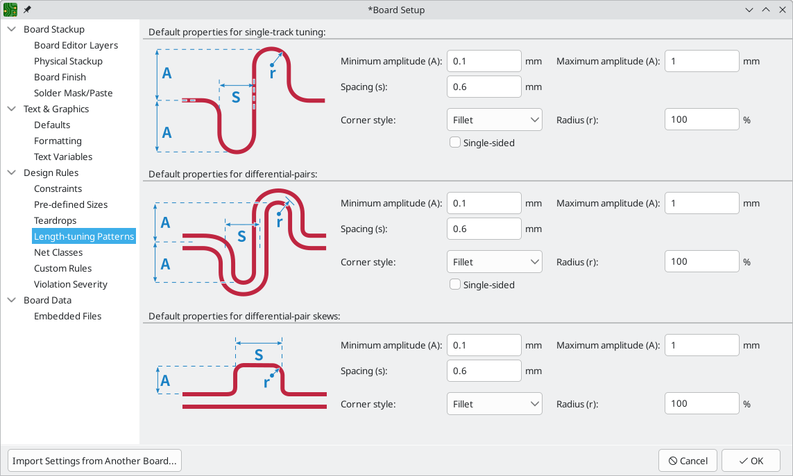
Length-tuning patterns
The length-tuning patterns section lets you set default parameters for each type of length-tuning pattern (single-track length, differential-pair length, and differential-pair skew). These defaults can be overridden in the properties of each tuning pattern added to the board. See the length tuning documentation for more information.
Net Classes
The Net Classes section allows you to configure routing and clearance rules for different classes of nets.
More than one net class can be assigned to a net. For nets with multiple net
classes assigned, an effective aggregate net class is formed, taking any net
class properties from the highest priority net class which has that property
set. Net class priority is determined by the ordering in the Schematic or Board
Setup dialogs. The Default net class is used as a fallback for any missing
properties after all explicit net classes have been considered; this means that
nets may be part of the Default net class even if they have other net classes
explicitly assigned.
Net classes may be created and edited in either the Schematic or Board Setup dialogs.
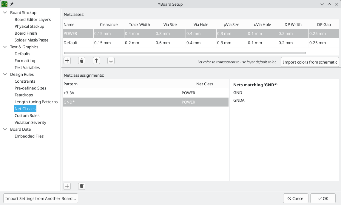
The upper portion of the Net Classes section contains a table showing the net classes in the design and the design rules that apply to each net class. Every class has values for copper clearance, track width, via sizes, and differential pair sizes. These values will be used when creating tracks and vias unless a more specific rule overrides them (see Custom Rules below).
No rule may override the minimum values set in the Constraints section of Board Setup. For
example, if you set a net class clearance to 0.1 mm, but the Minimum Clearance in the
Constraints section is set to 0.2 mm, nets in that class will have a clearance of 0.2 mm.
|
The track widths and via sizes defined for each net class are used when the track width and via size controls are set to "use netclass values" in the PCB editor. These widths and sizes are considered the default, or optimal, sizes for that net class. They are not minimum or maximum values. Manually changing the track width or via size to a different value from that defined in the Net Classes section will not result in a DRC violation. To restrict track width or via size to specific values, use Custom Rules.
Each net class can also have a color assigned to it. Depending on how net colors are configured in the appearance panel, net class colors can override the default color for ratsnest lines or copper objects. In addition to arbitrary colors for each net class, you can set all net classes to use the same color as configured for them in the schematic editor by clicking the Import colors from schematic button. To use a layer’s default color instead of overriding it with a custom net class color, set the net class color to transparent.
The lower portion of the Net Classes section lists pattern-based net class assignments. Working with pattern-based net class assignments is explained in the Schematic Editor documentation; pattern-based assignments can be edited in either the Board or Schematic Setup windows.
Note that pattern-based assignments can be created directly from the PCB editing canvas by right clicking a copper track or zone and clicking Assign netclass…. Net classes can also be assigned in the schematic using net class directives or labels instead of pattern-based assignments.
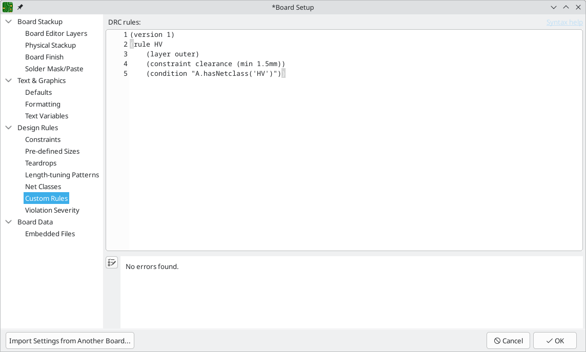
Custom Rules
The Custom Rules section contains a text editor for creating design rules using the custom rules language. Custom rules are used to create specific design rule checks that are not covered by the basic constraints or net class settings.
Custom rules will only be applied if there are no errors in the custom rules definitions. Use the Check Rule Syntax button to test the definitions and fix any problems before closing Board Setup.
See Custom Design Rules in the Advanced Topics chapter for more information on the custom rules language as well as example rules.
Violation Severity
The Violation Severity section allows you to configure the severity of each type of design rule check. Each rule may be set to create an error marker, a warning marker, or no marker (ignored).
| Individual rule violations may be ignored in the Design Rule Checker. Setting a rule to Ignore in the Violation Severity section will completely disable the corresponding design rule check. Use this setting with caution. |
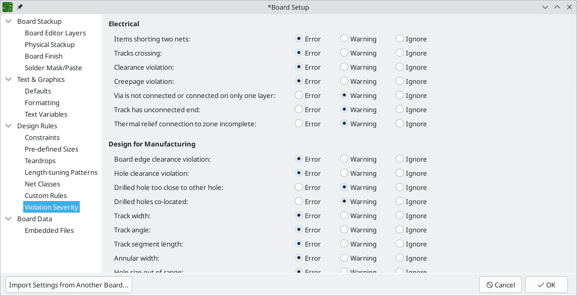
For descriptions of each violation type, and how to ignore individual violations without disabling all violations of that type, see the DRC documentation.
Embedding files
External files can be embedded within a board file. Embedding a file stores a copy of the file inside the board file. The design can then refer to the embedded copy of the file instead of the external file, which makes the project more portable as it doesn’t rely on an external file. Fonts, datasheets, drawing sheets, SPICE models, and footprint 3D models can be embedded and used within KiCad. Other arbitrary files can also be embedded to store them in the project for later export, but they are not used by any KiCad functionality. Files embedded in a board necessarily increase the board’s file size, although files are compressed before being embedded to minimize the space required.
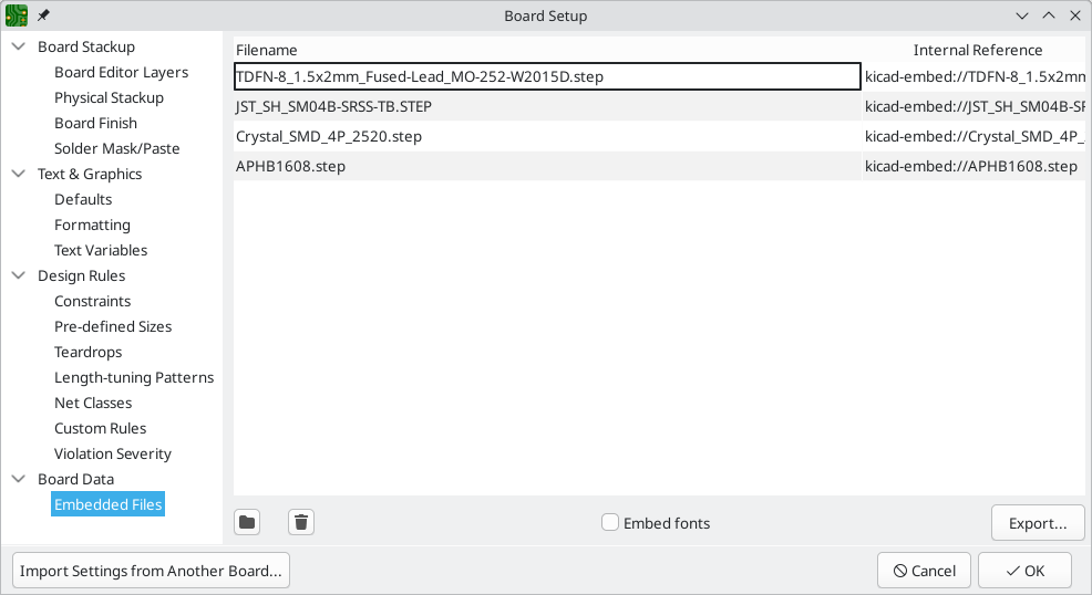
Embedded files are managed in the Embedded Files section of Board Setup. All files embedded in a board
are shown here. To embed a file inside a
board, click the ![]() button and select the file. The file is
then embedded inside the PCB and is listed in the embedded files list along with its
embedded reference. The embedded reference is a unique identifier for the embedded file that begins with
button and select the file. The file is
then embedded inside the PCB and is listed in the embedded files list along with its
embedded reference. The embedded reference is a unique identifier for the embedded file that begins with
kicad-embed://. You can use the embedded reference elsewhere in the Board Editor to refer to the
embedded file as if it were an external file path. You can copy the embedded reference by right
clicking and selecting Copy Embedded Reference. To remove an embedded file, click the
![]() button. Any remaining links to the removed file will become
invalid.
button. Any remaining links to the removed file will become
invalid.
| 3D models and drawing sheets can be embedded directly using the file browser when you add them to a footprint (3D models) or to a board (drawing sheets) by enabling the Embed Files option in the file browser. This is a single-step shortcut for adding the files in Board Setup and then referring to them by their embedded reference; the result is the same. |
To embed any fonts used in a board, check the Embed fonts checkbox. All fonts used in the board design will be embedded, so text using that font can be edited on any computer regardless of whether the font file is installed.
You can also embed files in a footprint, either in the board copy of a footprint or in a library. Such files will be available within the footprint instance but not within the larger board design or within other footprints. Files embedded in a footprint are deduplicated when the footprint is added to a board: if a file is embedded in a footprint, and multiple instances of that footprint are added to the board, only one copy of the file will be embedded, and all of the footprint instances will refer to the same embedded file.
As an example, to embed a 3D model in a project and use it within several footprints, you could embed the model using the Board Setup dialog, copy the internal reference, and paste the internal reference as a 3D model path in each footprint that uses that model. Alternatively, you could embed the model within a single footprint, either in the board or in the source footprint library. In this case, the footprint itself is portable if you export the footprints from the board, and the model embedding is managed in the footprint’s properties rather than Board Setup. A more convenient way to achieve the same thing, however, is to open the footprint’s properties dialog, add a 3D model file, and enable the Embed File option in the file browser. Again, this could be done for a footprint in the board or for a footprint in the source footprint library.
Files can also be embedded in schematics.
Importing settings
You can import part or all of the board setup from an existing board. This technique can be used to create a "template" board that has the settings you want to use on multiple designs, and then importing these settings from the template board into each new board rather than entering them manually.
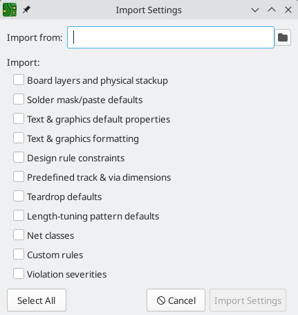
To import settings, click the Import Settings from Another Board… button at the bottom of the
Board Setup dialog and then choose the kicad_pcb file you want to import from. Select which
settings you want to import and the current settings will be overwritten with the values from the
chosen board.
The settings that are available to import are:
-
Board layers and physical stackup
-
Solder mask/paste defaults
-
Text and graphics default properties
-
Text & graphics formatting
-
Design rule constraints
-
Predefined track & via dimensions
-
Teardrop defaults
-
Length-tuning pattern defaults
-
Net classes
-
Custom rules
-
Violation severities