编辑电路板
放置和绘制操作
放置和绘图工具位于右边的工具栏中。 当一个工具被激活时,它将一直处于激活状态,直到选择了一个不同的工具或用 Esc 键取消该工具。 当任何其他工具被取消时,选择工具总是被激活。
某些工具栏按钮在调色板中有多个可用工具。这些工具由按钮右下角的小箭头表示:
要显示调色板,你可以在工具上点击并按住鼠标按钮,或者点击并拖动鼠标。 调色板关闭时将显示最近使用的工具。
|
Selection tool (the default tool). |
|
Local ratsnest tool: when the board ratsnest is hidden, selecting footprints with this tool will show the ratsnest for the selected footprint only. Selecting the same footprint again will hide its ratsnest. The local ratsnest setting for each footprint will remain in effect even after the local ratsnest tool is no longer active. |
|
Footprint placement tool: click on the board to open the footprint chooser, then click again after choosing a footprint to confirm its location. |
|
Route tracks / route differential pairs: These tools activate the interactive router and allow placing tracks and vias. The interactive router is described in more detail in the Routing Tracks section below. |
|
Tune length: These tools allow you to tune the length of single tracks or the length or skew of differential pairs, after they have been routed. See the Routing Tracks section for details. |
|
Add vias: allows placing vias without routing tracks. Vias placed on top of tracks using this tool will take on the net of the closest track segment and will become part of that track (the via net will be updated if the pads connected to the tracks are updated). Vias placed anywhere else will take on the net of a copper zone at that location, if one exists. These vias will not automatically take on a new net if the net of the copper zone is changed. |
|
Add filled zone: Click to set the start point of a zone, then configure its properties before drawing the rest of the zone outline. Zone properties are described in more detail below. |
|
Add rule area: Rule areas, formerly known as keepouts, can restrict the placement of items and the filling of zones and can also define named areas to apply specific custom design rules to. |
|
Draw lines. Note: Lines are graphical objects and are not the same as tracks placed with the Route Tracks tool. Graphical objects cannot be assigned to a net. |
|
Draw arcs: pick the center point of the arc, then the start and end points. By right clicking this button, you can change the arc editing mode between a mode that maintains the existing arc center and a mode that maintains the arc radius. |
|
Draw rectangles. Rectangles can be filled or outlines. |
|
Draw circles. Circles can be filled or outlines. |
|
Draw graphical polygons. Polygons can be filled or outlined. Note: Filled graphical polygons are not the same as filled zones: graphical polygons cannot be assigned to a net and will not keep clearance from other items. |
|
Add bitmap image. |
|
Add text. |
|
Add a textbox. |
|
Add dimensions. Dimension types are described in more detail below. |
|
Deletion tool: click objects to delete them. |
|
Set drill/place origin (used for fabrication outputs) or grid origin. |
|
Interactively measure the distance between two points. |
捕捉
移动、拖动和绘制电路板元素时,栅格、焊盘和其他元素可以具有捕捉点,具体取决于用户偏好设置中的设置。在复杂的设计中,捕捉点可能离得太近,这会使当前的工具操作变得困难。使用下表中的快捷键可以在移动鼠标时禁用栅格和对象捕捉。
| 快捷键 | 效果 |
|---|---|
Ctrl |
关闭网格捕捉。 |
Shift |
关闭对象捕捉。 |
编辑对象属性
所有对象都有可在对话框中编辑的属性。 使用快捷键 E 或从右键菜单中选择属性来编辑所选项目的属性。 只有当你选择的所有项目都是同一类型时,你才能打开属性对话框。 要想一次编辑不同类型的项目的属性,请参阅下面关于批量编辑工具的章节。
在属性对话框中,任何包含数字值的字段也可以接受一个基本的数学表达式,从而得到一个数字值。 例如,一个尺寸可以被输入为 2 * 2mm,结果是 4mm 的值。 支持基本算术运算符以及用于定义运算顺序的圆括号。
使用封装
Adding footprints to the board
Footprints are automatically added to the board when the PCB is updated from the schematic. The footprint associated with each schematic symbol is added to the board if it is not already present, and each footprint pad is associated with the corresponding symbol pin’s net. Symbol pins are matched to footprint pads by pin/pad number.
When footprints are added to the board after an update from the schematic, they are grouped by schematic sheet and by geographical location in the schematic. They are initially attached to the cursor; you can place them by clicking in the desired location.
You can also add footprints to the board manually using the Add Footprint tool (A or the ![]() button). Note that footprints added in this way will not be automatically associated with a symbol or have nets assigned to their pads, and subsequent updates from the schematic will remove these unassociated footprints unless the footprint is locked or the Delete footprints with no symbols option is unchecked in the Update PCB From Schematic dialog. For these reasons, it is usually recommended to avoid manually adding footprints to the board. Manually adding footprints is necessary for PCB-only workflows, and can also be useful for adding logos or other footprints that do not need a corresponding schematic symbol.
button). Note that footprints added in this way will not be automatically associated with a symbol or have nets assigned to their pads, and subsequent updates from the schematic will remove these unassociated footprints unless the footprint is locked or the Delete footprints with no symbols option is unchecked in the Update PCB From Schematic dialog. For these reasons, it is usually recommended to avoid manually adding footprints to the board. Manually adding footprints is necessary for PCB-only workflows, and can also be useful for adding logos or other footprints that do not need a corresponding schematic symbol.
Placing and moving footprints
Once footprints have been added to the board, you can reposition them in many ways.
The Move command (M) moves a footprint or a selection of footprints, ignoring any connected track segments that are not selected. No DRC checking is done when moving footprints with the Move command.
There is a reference point for the move operation, which is the point in the footprint which attaches to the cursor and therefore the point in the footprint that snaps to the grid and to other objects. The reference point during a move is determined by the location of the cursor when the Move command is initiated. If the cursor is over a pad, the pad’s center will be used as the reference point. If the cursor is not over a pad, the footprint’s anchor (coordinate origin point) will be used. To select an arbitrary snapping point, you can use the Move With Reference command instead of the regular Move command (right click → Positioning Tools → Move with Reference). After initiating the command, click on the desired reference point; KiCad will then begin the move with that point as the reference.
You can also use the Drag command (D) to move the selected footprint using the interactive router, maintaining all track connections to the footprint. Dragging footprints behaves like the Highlight Collisions router mode: obstacles will not be avoided or shoved, only highlighted. Only one footprint at a time can be dragged.
Flip a footprint to the opposite side of the board with the F hotkey. Any parts of the footprint on a front layer will be swapped to the corresponding back layer, and vice versa.
Rotate a footprint counter-clockwise using the R hotkey, or clockwise using Shift+R. By default, footprints are rotated by 90 degrees every time the rotate command is used, but you can configure the rotation angle step in Preferences → PCB Editor → Editing Options.
You can directly set a footprint’s exact absolute position, rotation angle, and PCB side using either the Footprint Properties dialog or the Properties panel.
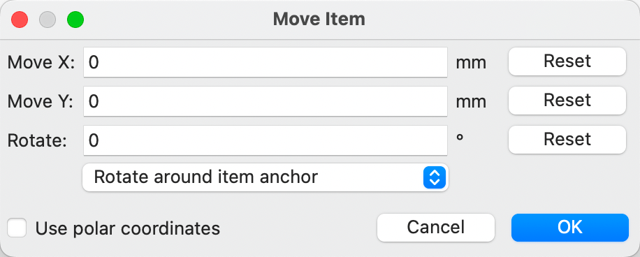
To reposition a footprint relative to its current position, use the Move Exactly tool (Shift+M). The dialog lets you specify an X and Y translation, as well as a rotation, that will be applied to the footprint. The rotation can be performed relative to either the footprint’s anchor, the local coordinate origin, or the drill/place origin. You can also use polar coordinates instead of Cartesian coordinates.
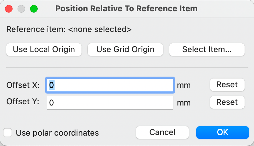
To position a footprint relative to another object, you can use the Position Relative tool (Shift+P). With this tool, you select a reference point for the move, which can be the local origin, the grid origin, or another arbitrary point, such as a pad in another footprint. The selected footprint is moved to the specified offset from the reference point.
You can swap the position of two selected footprints using the Swap command (Shift+S). The first footprint is assigned the location, rotation, and board side of the second footprint, and vice versa. If there are more than two footprints selected, the locations are cycled: the last footprint gets the position of the first footprint, the first footprint gets the location of the second, and so on.
There are several convenience features that make it easier to find, select, and move specific footprints or footprints related to another footprint.
The Get and Move Footprint command (T) prompts you to choose a footprint from a list or by typing a reference designator. KiCad then attaches the chosen footprint to your cursor for a move operation.
There are two commands to select other footprints that need to be connected to the selected footprint but don’t yet have routed connections. The Select All Unconnected Footprints command (O) selects all footprints that have ratsnest lines to the currently selected footprints. The command can be executed repeatedly to further expand the selection based on the newly selected items. The Grab Nearest Unconnected Footprint command (Shift+O) selects the closest footprint with ratsnest lines to the currently selected footprint, and additionally begins to move it. If there are multiple footprints initially selected, the command will act like the Move Individually command described below, individually moving the closest unconnected footprint for each of the initially selected footprints.
You can select footprints based on their schematic sheet using the right click → Select → Items in Same Hierarchical Sheet command, which selects all other footprints that are in the same schematic sheet as the originally selected footprint.
If you want to move multiple selected footprints in sequence, use the Move Individually command (Ctrl+M). After triggering the command, KiCad will begin moving the first selected footprint. After you click to place the footprint, KiCad will immediately start moving the next footprint, in the same order that you selected the footprints. You can skip moving a footprint by pressing Tab, commit the current move and skip any remaining moves by double-clicking, or cancel all moves (including those already completed) by pressing Esc.
If you want to move a collection of footprints at once into one area, the Pack and Move Footprints command (P) closely packs the selected footprints together and moves them as a block.
| Move Individually and Pack and Move Footprints are useful in combination with other selection convenience features, such as cross-selection from the schematic or the advanced footprint selection features described above. For example, you could select a group of bypass capacitors in the Schematic Editor, switch to the PCB Editor where the corresponding footprints are now selected, and then use Move Individually to quickly place all of the bypass capacitor footprints close to their respective ICs. Alternatively, you could use one of the other selection tools, such as Select All Unconnected Footprints, to select many footprints from all over the board, then use Pack and Move Footprints to quickly put them all into a small area. |
Finally, KiCad can automatically place footprints onto the board. The auto-place function attempts to optimally place footprints to simplify ratsnest connections to other footprints. You can auto-place the selected footprints with Place → Auto-Place Footprints → Place Selected Footprints, or auto-place all footprints outside of the board outline with Place → Auto-Place Footprints → Place Off-Board Footprints.
封装属性
| This section of the KiCad documentation has not yet been written. We appreciate your patience as our small team of volunteer documentation writers work to update and expand the documentation. |
Editing Footprints
| This section of the KiCad documentation has not yet been written. We appreciate your patience as our small team of volunteer documentation writers work to update and expand the documentation. |
使用焊盘
在将封装放置在电路板上之后,可以检查和编辑封装的每个单独的焊盘的属性。 换句话说,如果库中的封装设计不合适,就可以在电路板上封装的特定实例中覆盖单个封装焊盘的设计。 例如,你可能希望为一个需要在特定设计中保持不焊接的焊盘去除焊膏孔,或者你可能希望移动一个轴向引线电阻的通孔焊盘的位置,以适应特定的设计。
| 默认情况下,所有封装焊盘的位置都被锁定,因此可以编辑焊盘属性,但不能移动焊盘相对于封装其他部分的位置。 焊盘可以被解锁以允许自由移动,这对某些应用很有用(如具有不同引线位置的通孔封装),但通常不建议用于表面贴装封装。 |
当一个焊盘被选中时,焊盘属性对话框将通过上下文菜单或默认的快捷键E打开。 请注意,KiCad 认为如果你在焊盘附近点击,你可能是想选择整个封装而不是单个焊盘。 要选择单个焊盘,请确保在焊盘区域内点击,或者关闭选择过滤器中的 "封装" 设置(并确保 "焊盘" 设置打开),以防止意外地选择整个封装而不是特定的焊盘。
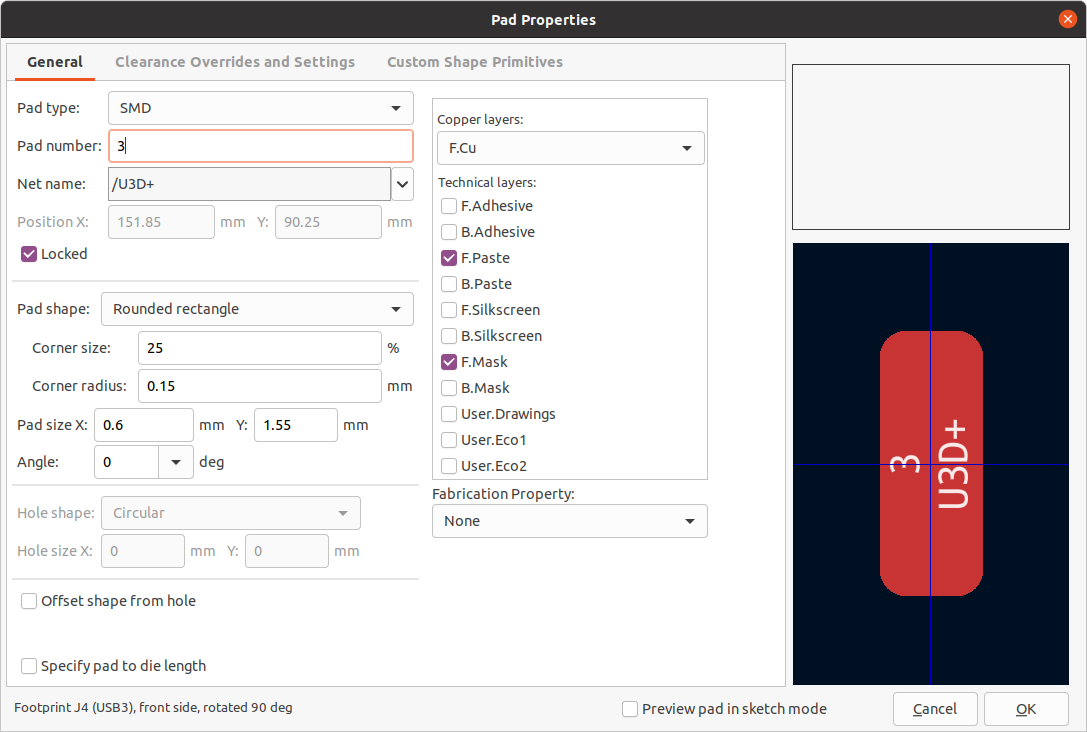
焊盘属性对话框的常规选项卡显示了焊盘的物理属性,包括它的几何、形状和层设置。
焊盘类型: 此设置控制焊盘的哪些功能被启用。
SMD 焊盘是电连接的,没有孔。 换句话说,它们存在于一个单一的铜层上。
通孔 焊盘是电气连接的,有一个电镀孔。 孔存在于每一层,而铜焊盘存在于多层(见下文 铜层 设置)。
板边连接器 焊盘是允许与 Edge.Cuts 层上的电路板边框重叠的 SMD 焊盘。
NPTH,机械 焊盘是没有电镀的通孔,不具有电气连接。
SMD 光圈 焊盘是没有孔和没有电连接的焊盘。 这些可用于在技术层上添加特定的设计,例如锡膏或焊接掩模孔径。(SMD 定位孔)
铜层 设置控制哪些铜层将有一个与焊盘相关的形状。
对于 SMD 焊盘,选项是 F.Cu 或 B.Cu,控制焊盘是在电路板的前面还是后面 相对于封装的位置。 换句话说,如果一个焊盘在其属性中被设置为存在于 B.Cu 上,而封装被翻转到电路板的背面,该焊盘现在将存在于 F.Cu 上,因为它也被翻转了。
对于通孔焊盘,有可能从焊盘与其他铜(布线或填充区)没有电气连接的铜层中移除焊盘形状。 将铜层设置为 连接层 将从任何未连接层移除焊盘形状,而设置为 F.Cu、B.Cu 和连接层 将从任何内部未连接层移除焊盘形状。 这在密集的电路板设计中很有用,可以增加内部层的可布线面积。
技术层 复选框控制哪些技术层会有一个与焊盘形状相同的孔径。 默认情况下,焊盘在粘贴层和屏蔽层上的孔径与铜层相匹配。
| 在当前版本的 KiCad 中,不可能在不同的铜层上定义不同的焊盘形状或尺寸。 |
指定焊盘到模具的长度: 此设置允许将一个长度与此焊盘相关联,该长度将被布线长度调整工具和网络检测器添加到布线的长度中。这可以用来指定内部键合线的长度,以便更准确地进行长度匹配,或者在其他情况下,网络的电气长度长于电路板上的布线的长度。
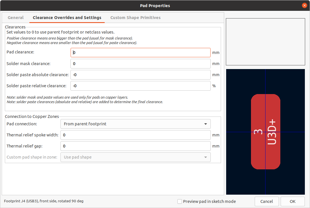
出现在任何技术层上的孔径将具有与铜层上的焊盘形状相同的形状和尺寸。 在 PCB 制造过程中,制造商经常会改变掩膜和浆料孔径相对于铜焊盘尺寸的相对尺寸,但由于这种尺寸变化是特定于制造过程的,大多数制造商希望在提供设计数据时将孔径设置为与铜焊盘相同的尺寸。 对于需要在设计数据中加大或缩小技术层孔径的特定情况,你可以使用 "覆盖" 标签中的设置。
焊盘间隙 控制焊盘与不同网络上的任何铜形状(布线、通孔、焊盘、区域)之间的最小间隙。 这个值通常被设置为 0,这将导致焊盘的间隙被继承自封装上设置的任何间隙覆盖,或者电路板的设计规则和网络类规则(如果封装的间隙也被设置为 0)。
焊接掩模间隙 控制 F.Mask 和 B.Mask 层上的焊盘形状和孔径形状之间的尺寸差异。 一个正数意味着焊接掩模孔径将大于铜的形状。 这个数字是一个适用于所有方向的膨胀。 例如,这里的 0.1mm 值将导致阻焊孔径膨胀 0.1mm,这意味着在焊盘的所有侧面将有 0.1mm 的边界,当沿给定轴线测量时,阻焊开口将比焊盘宽 0.2mm。
焊膏绝对间隙 控制 F.Paste 和 B.Paste 层上焊盘形状和孔径形状之间的尺寸差异。 它的行为在其他方面与 焊膏间隙 设置的行为相同。
焊膏相对间隙 允许将焊膏间隙值设置为焊盘尺寸的百分比,而不是绝对距离值。 如果同时指定了相对间隙和绝对间隙,它们将被加在一起以确定锡膏孔径的大小。
"覆盖" 选项卡还可以控制焊盘如何连接到任何与之重叠并共享其网络的铜区。
焊盘连接 控制焊盘是否与区段有实心的、散热的或无连接。 与其他覆盖项一样,这个覆盖项可以为单个垫块或整个封装设置。 这个控制的默认设置是 从父系封装,而默认的封装设置是使用区段属性中指定的连接模式。
散热辐条宽度 控制区段连接模式为散热时产生的辐条的宽度。
散热间隙 控制散热条的长度,或焊盘的形状和区域的填充铜面积之间的间隙。
区域内的自定义焊盘形状 当焊盘使用自定义形状而不是默认形状之一时,控制区域填充器的行为。 这可以用来在使用散热条和自定义焊盘形状时实现不同的结果。
使用区域
铜区,有时也被其他 EDA 工具称为铜岛或填充,是分配给一个特定网络的实心或多边形的铜区,自动保持与其他铜对象的间隙。 铜区通常用于填充板层(或板层的一部分)上的所有自由空间,以创建接地和电源平面,承载大电流,或提供屏蔽。
| 一些 EDA 工具有单独的工具用于创建 "放置层" 和在信号层上创建铜区。 在 KiCad 中,铜区工具被用于这两种应用。 |
区域是由一个多边形的 边框 来定义的,它定义了填充铜区的最大范围。 这个边框并不代表物理铜,也不会出现在导出的制造数据中。 每次修改边框或边框内的任何对象时,该区的实际铜区必须被 填充。 填充过程可以在单个区上运行,也可以在电路板的所有区上运行(默认快捷键 B)。 区域可以 不填充(默认快捷键 Ctrl+B),以提高性能并减少编辑大板时的视觉混乱。
| By default, zone filling is a manual process rather than occurring every time an object changes that would result in a change to the zone copper. This is because zone filling can be a slow process on older computers or very large designs. It is important to make sure zone fills are up-to-date before generating outputs. KiCad will check that zones have been updated and warn you before generating outputs or running DRC when zones have not yet been refilled. You can optionally enable automatic zone-filling in the Preferences dialog (PCB Editor → Editing Options → Miscellaneous → Auto-refill zones). |
To draw a zone, click the Add Filled Zone tool (![]() ) on the right toolbar, or use default hotkey Ctrl+Shift+Z. Click to choose the first point of the zone outline. The Zone Properties dialog will appear, allowing you to choose the zone net and other properties. These properties may be edited at any time, so it is not critical to choose them all correctly at first. Accept the dialog and continue placing points to define the zone outline. To finish the zone, double-click to set the last point. Zone outline points may be modified like graphic polygons, by dragging the square handles to move a corner or dragging the circular handles to move an edge. To edit the zone’s properties, use hotkey E or select Properties from the context menu.
) on the right toolbar, or use default hotkey Ctrl+Shift+Z. Click to choose the first point of the zone outline. The Zone Properties dialog will appear, allowing you to choose the zone net and other properties. These properties may be edited at any time, so it is not critical to choose them all correctly at first. Accept the dialog and continue placing points to define the zone outline. To finish the zone, double-click to set the last point. Zone outline points may be modified like graphic polygons, by dragging the square handles to move a corner or dragging the circular handles to move an edge. To edit the zone’s properties, use hotkey E or select Properties from the context menu.
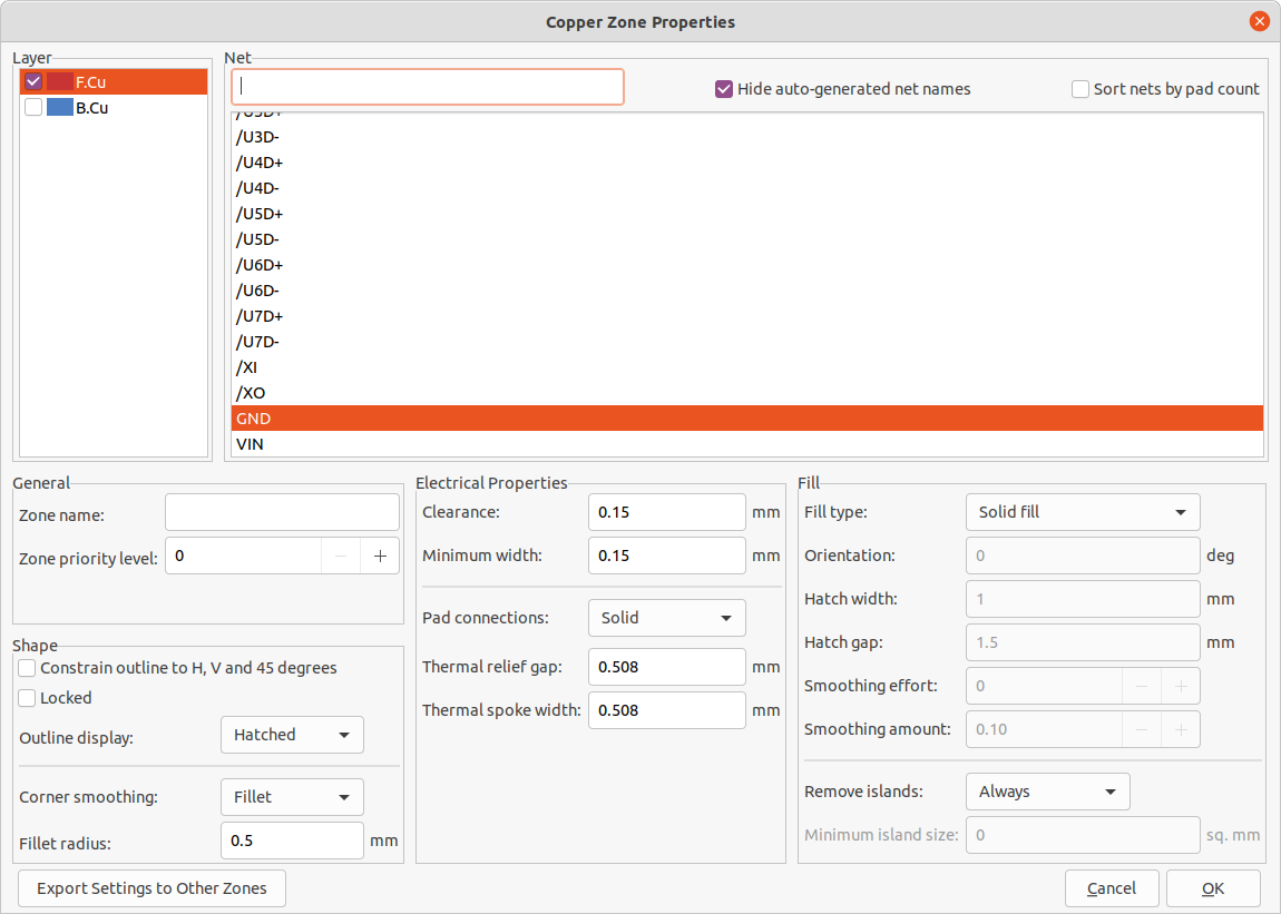
层: 一个区域对象可以在一个或多个铜层上创建填充铜。 勾选每个铜层旁边的方框,这个区域边框应该在这些铜层上填充。 每个层上的铜将被独立地填充,但所有层将共享同一个网络。
网络: 选择该区铜区应连接的电气网络。 可以创建没有网络分配的区域。 没有网络的区域将与任何网络上的任何铜对象保持间隙。
区域名 可以用来给一个区域指定一个特定的名称。 这个名字可以用来在自定义的 DRC 规则中指代该区域。
Zone priority level determines the order in which multiple zones on a single layer are filled. The highest priority level zone on a given layer will be filled first. Lower-priority zones will keep clearance to the filled areas of higher-priority zones. Two zones on the same layer with the same priority level will overlap (short-circuit) with each other, unless they are assigned different nets. When two zone outlines with the same priority and different nets touch, one zone will maintain clearance to the other so that they don’t short.
限制边框为 H、V 和 45 度 控制区域边框绘制工具的 初始 行为。 当这个选项被启用时,区域边框将被限制在 45 度的角度。 请注意,在创建了区域边框之后,这个选项就没有作用了。 边框点在创建后可以自由修改。
锁定 控制区域边框对象是否被锁定。 被锁定的对象不能被操作或移动,也不能被选择,除非在选择过滤器面板中启用 锁定的项目 选项。
边框显示 控制区域边框在屏幕上的绘制方式。 在 直线 模式下,只绘制边框的边界线。 在 阴影 模式下,阴影线会在边框边界的内侧绘制一小段距离,以使区段边框更加明显。 在 完全阴影 模式下,阴影线被绘制在整个区域边框的内部。
拐角平滑 控制边框拐角处的填充铜区的行为。拐角可以通过倒角或圆角来平滑,如果平滑被禁用,也可以一直延伸到边框的拐角。
| 默认情况下,倒角和圆角不会被添加到区域边框的内角,因为这将导致填充的铜延伸到边框之外。 如果需要光滑的内角,请在电路板设置对话框的约束部分启用 允许区域边框外的圆角 选项。 |
间隙 控制该区域的填充区域与其他铜质物体保持的最小间隙。 请注意,如果两个间隙值有冲突,将使用较大的间隙值。 例如,如果一个区被设置为使用 0.2 毫米的间隙,但其网络类被设置为使用 0.3 毫米的间隙,结果将是 0.3 毫米的间隙。
最小宽度 控制在该区域内产生的铜间隙的最小尺寸。 任何低于这个最小宽度的铜区都会在填充过程中被移除。
焊盘连接 控制填充区与同一网络上的封装焊盘的连接方式。 实心 连接将导致铜完全重叠在焊盘上。散热焊盘 将导致小铜辐条连接焊盘和铜区的其余部分,增加焊盘和区的其余部分之间的热阻。 这对手工焊接很有用。 对 PTH 的散热焊盘 将对电镀通孔焊盘应用散热焊盘,并对表面贴装焊盘使用固体连接。 无 将导致该区不连接到同一网络上的任何焊盘。
散热间隙 控制任何焊盘和铜区之间保持的距离,当焊盘连接模式被设置为产生散热。
散热宽度 控制 "辐条" 的宽度,即连接焊盘和其他铜区的短铜段。
填充类型 控制铜区的填充方式:默认为 实心填充,这将导致铜填充在区域边框内的所有可用空间。 该区域也可以被设置为 填充图案,这将使该区域充满含铜量较少的图案。
方向 控制孵化图案线的角度。 一个 0 度的方向将导致孵化图案使用水平和垂直的线条。
填充宽度控制填充图案中每条线的宽度。
填充间隙 控制填充图案中每条线之间的距离。
平滑效果 控制应用于填充图案的平滑风格。 0 的值将导致无平滑,3 的值将导致最精细的平滑。 更高的值将导致更长的处理时间和更大的 Gerber 文件。
平滑量 是一个比率,控制平滑倒角或圆角的大小,当 平滑效果 被设置为 0 以外的值时,会产生平滑倒角。
移除孤岛 控制初始区域填充后孤立的铜区(也称为孤岛)的行为。 当设置为 总是 时,区域内的孤立区域会被移除。当设置为 从不 时,孤立区域会被搁置,并会导致铜区不与网络的其他部分连接。 当设置为 低于区域限制时,可以指定一个 **最小的孤岛尺寸,低于这个阈值的孤岛将被删除。
| Regardless of the remove islands setting, islands are never removed from zones that are electrically unconnected. In other words, islands are only removed from zones that have at least one electrical connection. |
图形对象
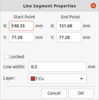
图形对象 (直线、圆弧、矩形、圆、多边形和文本)可以存在于任何图层上,但不能分配给网络。矩形、圆和多边形可以在其属性对话框中设置为填充或边框。线宽属性将控制边框的宽度,即使是填充形状也是如此。填充形状的线宽可以设置为 "0" 以禁用边框。
正在创建图形形状
The right toolbar can be used to create lines (![]() , default hotkey Ctrl+Shift+L), arcs (
, default hotkey Ctrl+Shift+L), arcs (![]() , default hotkey Ctrl+Shift+A), rectangles (
, default hotkey Ctrl+Shift+A), rectangles (![]() ), circles (
), circles (![]() , default hotkey Ctrl+Shift+C), and polygons (
, default hotkey Ctrl+Shift+C), and polygons (![]() , default hotkey Ctrl+Shift+P).
, default hotkey Ctrl+Shift+P).
矩形、圆形和多边形可以是填充形状或边框。 线宽 选项控制边框的宽度。 边框宽度在图形对象的 "理想" 形状的两边延伸。 例如,一个被定义为半径为 2 毫米、线宽为 0.2 毫米的图形圆将由一个外半径为 2.2 毫米、内半径为 1.8 毫米的圆环组成。 如果启用了 填充形状 选项,并且线宽被设置为 0,该形状将是一个半径为 2 毫米的填充圆。
Arcs have two editing modes, which are selectable in Preferences → PCB Editor → Editing Options or by right clicking the ![]() button on the right toolbar. The first mode (keep arc center, adjust radius) maintains the position of the arc center as as the arc endpoints or midpoint are dragged, changing the radius as necessary. The second mode (keep arc endpoints or direction of starting point) maintains the position of the arc endpoints and the arc’s direction of curvature as the midpoint or center are dragged.
button on the right toolbar. The first mode (keep arc center, adjust radius) maintains the position of the arc center as as the arc endpoints or midpoint are dragged, changing the radius as necessary. The second mode (keep arc endpoints or direction of starting point) maintains the position of the arc endpoints and the arc’s direction of curvature as the midpoint or center are dragged.
正在创建文本对象
图形文字可以通过使用右侧工具栏的(![]() )图标或键盘快捷键 Ctrl+Shift+T 来放置。 点击来放置文本原点,然后在出现的对话框中编辑文本及其属性:
)图标或键盘快捷键 Ctrl+Shift+T 来放置。 点击来放置文本原点,然后在出现的对话框中编辑文本及其属性:
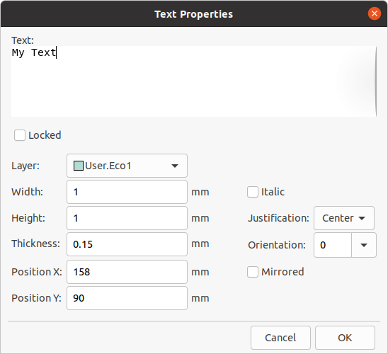
文字可以放在任何层上,但要注意,铜层上的文字不能与网络关联,不能与布线或焊盘形成连接。 铜区将填充在文字对象的矩形边界框周围。
Text supports markup for superscripts, subscripts, overbars, evaluating project variables, and accessing symbol field values.
| Feature | Markup Syntax | Result |
|---|---|---|
Superscript |
|
textsuperscript |
Subscript |
|
textsubscript |
Overbar |
|
text |
|
variable_value |
|
|
field_value of symbol refdes |
| Variables must be defined in Board Setup before they can be used. There are also a number of built-in text variables. |
电路板边框 (边缘切割)
KiCad 使用 Edge.Cuts 层上的图形对象来定义电路板的边框。 该边框必须是一个连续(封闭)的形状,但可以由不同类型的图形对象组成,如线和弧,或者是一个单一的对象,如矩形或多边形。 如果没有定义电路板的边框,或者电路板的边框无效,那么一些功能,如 3D 查看器和一些设计规则的检查将无法发挥作用。
批量编辑文本和图形
文本和图形的属性可以通过 编辑文本和图形属性 对话框(工具 → 编辑文本和图形属性…)来进行批量编辑。
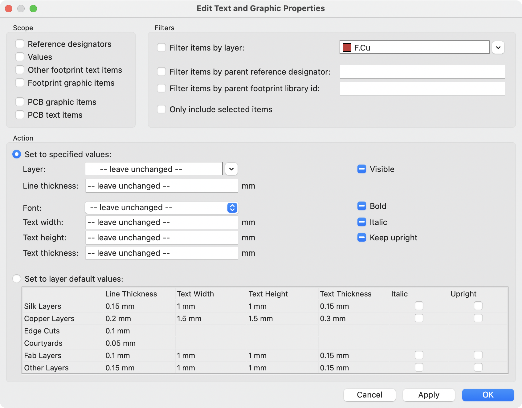
范围和筛选器
范围 设置限制了该工具只能编辑某些类型的对象。如果没有选择任何作用域,就不会有任何东西被编辑。
筛选器 限制该工具在选定的范围内编辑特定的对象。只有当对象符合所有启用的相关筛选器时才会被修改(有些筛选器不适用于某些类型的对象。例如,父封装筛选器不适用于图形项目,在改变图形属性时被忽略)。如果没有启用筛选器,所选范围内的所有对象都将被修改。对于带有文本框的筛选器,支持通配符。\* 匹配任何字符,? 匹配任何单个字符。
按层筛选项目 筛选到指定板层上的项目。
按名称筛选其他符号字段 筛选到指定的符号字段。
按父系位号筛选项目 筛选到封装中具有位号的字段。通过父系封装库 ID 筛选项目 筛选到封装中具有指定库标识符的字段。
只包括选定的项目 筛选到当前选择。
操作
被筛选对象的属性可以在对话框的底部设置为新值。通过选择 设置为指定值,可以将属性设置为任意值,或者通过选择*设置为图层默认值*,将属性重置为其图层的默认值。
下拉列表和文本框可以被设置为 --保持不变-- 以保留现有值。复选框可以被选中或不被选中,以启用或禁用一个变化,但也可以切换到第三个 "保持不变" 状态。
所有项目都可以设置其 层。
图形项目可以修改其 线的厚度。
可以修改的文本属性有 字体、文本宽度、文本高度、文本厚度(仅限 KiCad 字体)、强调(粗体 和 重体)和方向(保持直立)。封装文本也可以设置其 可见性。
标注
Dimensions are graphical objects used to show a measurement or other marking on a board design. They may be added on any drawing layer, but are normally added to one of the User layers. KiCad currently supports five different types of dimension: aligned, orthogonal, center, radial, and leader.
对齐 标注 (![]() ) 表示两点之间距离的测量。
测量轴是连接这两个点的线,标注图形与该轴保持平行。
) 表示两点之间距离的测量。
测量轴是连接这两个点的线,标注图形与该轴保持平行。
正交 标注 (![]() ) 也测量两点之间的距离,但测量轴是 X 轴或 Y 轴。
换句话说,这些标注表示两点之间距离的水平或垂直分量。
创建正交标注时,在选择要测量的两个点后,可以根据放置标注的位置选择要用作测量轴的轴。
) 也测量两点之间的距离,但测量轴是 X 轴或 Y 轴。
换句话说,这些标注表示两点之间距离的水平或垂直分量。
创建正交标注时,在选择要测量的两个点后,可以根据放置标注的位置选择要用作测量轴的轴。
中心 标注 (![]() ) 创建一个十字标记来指示一个点或圆或圆弧的圆心。
) 创建一个十字标记来指示一个点或圆或圆弧的圆心。
Radial dimensions (![]() ) show a measurement between
a center point and the outside of a circle or arc. The center point is indicated by a cross.
) show a measurement between
a center point and the outside of a circle or arc. The center point is indicated by a cross.
引线 标注 (![]() ) 创建一个箭头,将一条引线连接到文本字段。
此文本字段可以包含任何文本以及文本周围的可选圆形或矩形框。
这种类型的标注通常用来提醒人们注意设计的某些部分,以便在制造说明中参考。
) 创建一个箭头,将一条引线连接到文本字段。
此文本字段可以包含任何文本以及文本周围的可选圆形或矩形框。
这种类型的标注通常用来提醒人们注意设计的某些部分,以便在制造说明中参考。
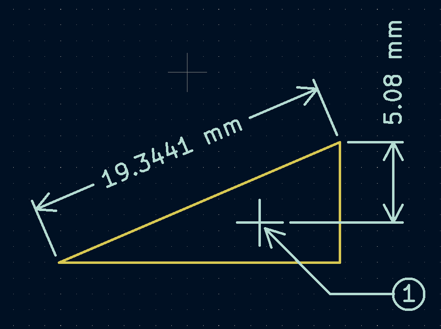
创建一个标注后,可以编辑其属性(快捷键 E)以改变显示数字的格式以及文本和图形线的风格。
| 您可以在电路板设置对话框的文本和图形默认值部分自定义新创建的标注对象的默认样式。 |
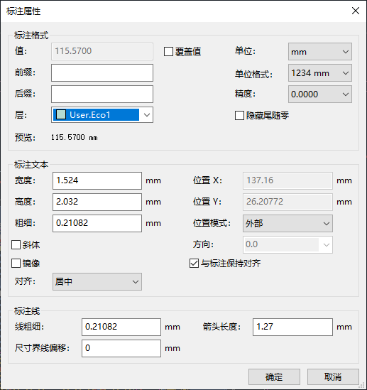
标注格式选项
覆盖值: 启用后,您可以直接在 值 字段中输入测量值,而不是实际测量值。
前缀: 此处输入的任何文字都将显示在测量值之前。
后缀: 此处输入的任何文字都将显示在测量值之后。
图层: 选择标注对象存在的层。
单位: 选择显示测量值的单位。 当更改电路板编辑器的显示单位时,自动 单位会导致标注单位发生变化。
单位格式: 从几种内置的单位显示风格中选择。
精度: 选择要显示多少位的精度。
标注文本选项
大多数标注文本选项与其他图形文本对象的选项相同(见上面的图形对象部分)。 也有一些特殊的选项适用于标注文本:
批注模式: 选择是手动定位批注文本,还是自动保持与批注测量线对齐。
与标注对齐: 开启后,标注文本的方向会自动调整,使文本与测量轴平行。
标注线选项
线条粗细: 设置构成标注形状的图形线的粗细。
标注界线偏移: 设置测量点到标注界线起点的距离。
箭头长度: 设置标注的形状的箭头段的长度。
引线选项
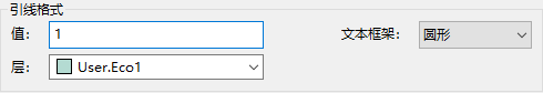
值: 输入要在引线行末尾显示的文本。
文本框架: 选择所需的文本周围的边界(圆形、矩形或无)。
布线
KiCad 具有交互式布线器的功能:
-
Allows manual or guided (semi-automatic) routing of single tracks and differential pairs
-
可通过以下方式修改现有设计:
-
拖动现有布线时重新布线现有布线
-
拖动封装时重新布线连接到封装焊盘的布线
-
-
允许通过插入蛇形线 + 来调整布线长度和差分对的偏移(相位) 为具有严格时序要求的设计调整布线形状
默认情况下,布线器在放置布线时尊重配置的设计规则:新布线的尺寸(宽度)将取自设计规则,在确定新布线和过孔的放置位置时,布线器将尊重设计规则中设置的铜间隙。 如果需要的话,可以通过使用高亮冲突布线器模式和打开布线器设置中的允许 DRC 违规选项来禁用这种行为(见下文)。
布线器有三种模式,可以随时选择。 布线器模式用于布线新布线,但也用于使用拖动(快捷键 D)命令拖动现有布线时。 这些模式是:
-
高亮冲突:在此模式下,大部分布线器功能被关闭,布线完全手动。 布线时,冲突 (间隙违规) 将以绿色高亮,如果存在冲突,则新布线的布线无法修复,除非打开了允许 DRC 冲突选项。 在此模式下,一次最多可以放置两个布线段 (例如,一个水平线段和一个对角线段)。
-
推挤:在此模式下,被布线的线段将绕过无法移动的障碍物 (例如,焊盘和锁定的布线/孔孔)和 推挤 障碍,这些障碍物可以移开。布线器在此模式下防止违反 DRC:如果无法布线到不违反 DRC 的光标位置,则不会创建新的布线。
-
绕走:在此模式下,布线器的行为与推挤模式相同,只是不会移动障碍物。
使用哪种模式是一个偏好问题。 对于大多数用户,我们建议使用推挤模式以获得最高效的布线体验,或者,如果您不希望布线器修改未被布线的线段,则建议使用绕走模式。请注意,推挤和绕走模式始终创建水平、垂直和 45 度 (H/V/45) 布线段。如果需要使用 H/V/45 以外的角度布线段,则必须使用高亮碰撞模式,并在交互布线器设置对话框中启用自由角度模式选项。
有五个主要的布线功能。单布线、差分对布线、调整单布线长度、调整差分对的长度和调整差分对的偏移 (相位)。 所有这些都存在于顶部工具栏上的路由菜单下拉菜单(单独)和绘图工具栏上的两个重载图标中,在右侧的绘图工具栏上。 上面介绍了重载图标的使用。 一个用于两个布线功能,一个用于三个调谐功能。 此外,布线菜单允许选择设置层对和交互式布线器设置。
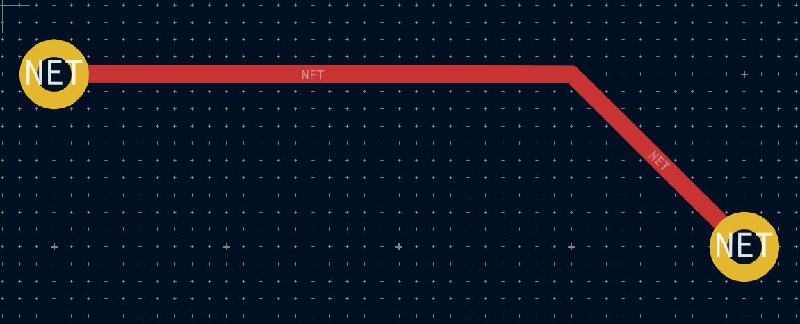
To route tracks, click the Route Tracks ![]() icon (from the drawing toolbar or from the top toolbar under Route) or use the hotkey X. Click on a starting location to select which net to route and begin routing. The net being routed will automatically be highlighted and the allowable clearance for the net will be indicated with a gray outline around the tracks being routed. The clearance outline can be disabled by changing the Clearance Outlines setting in the Display Options section of the Preferences dialog.
icon (from the drawing toolbar or from the top toolbar under Route) or use the hotkey X. Click on a starting location to select which net to route and begin routing. The net being routed will automatically be highlighted and the allowable clearance for the net will be indicated with a gray outline around the tracks being routed. The clearance outline can be disabled by changing the Clearance Outlines setting in the Display Options section of the Preferences dialog.
| 间隙边框显示从布线网络到 PCB 上任何其他铜线的最大间隙。 可以使用自定义设计规则为不同对象指定网络的不同间隙。 布线器将考虑这些间隙,但仅直观地显示最大间距值。 |
当布线器处于活动状态时,将从布线起点到编辑器光标绘制新的线段。这些线段是未固定临时 (unfixed temporary) 对象,它们显示当您使用左击或 Enter 键来固定布线 (fix the route) 时将创建哪些线段。非固定布线段以比固定布线段更亮的颜色显示。当您使用 Esc 键或通过选择另一个工具退出布线器时,将只保存固定布线段。完成布线操作(快捷键 End) 将固定所有布线并退出布线器。
在布线时,可以使用撤消最后一个布线段命令 (快捷键 Backspace) 取消固定最近固定的布线。您可以重复使用此命令以后退已固定的布线。
In previous versions of KiCad, using the left mouse button or Enter to fix the routed segments would fix all segments up to but not including the segment ending at the mouse cursor location. In KiCad 6 and later, this behavior is optional, and by default, all segments including the one ending at the mouse cursor location will be fixed. The old behavior can be restored by disabling the "Fix all segments on click" option in the Interactive Router Settings dialog.
布线时,可以按住 Ctrl 键禁用网格捕捉,按住 Shift 键禁用对焊盘和过孔等对象的捕捉。
| 也可以通过更改首选项对话框的编辑选项部分中的磁吸点首选项来禁用对对象的捕捉。 我们建议您在一般情况下保持启用对象捕捉,这样就不会意外地在焊盘或过孔上略微偏离中心结束布线。 |
布线形态
在垂直(H) / 水平 (V) / 45 度模式下布线时,形态 是指一组两个线段如何连接单个 H/V/45 度线段无法到达的两个点。 在这种情况下,这些点将由一条水平或垂直线段和一条对角线 (45度) 线段连接。形态指的是这些线段的顺序:是水平/垂直线段还是对角线线段在前。

KiCad 的布线器试图根据一系列因素自动选择最佳形态。一般说来,布线器会尝试最大限度地减少路线中的拐角数量,并尽可能避免 "坏" 拐角 (如锐角)。当从焊盘布线或布线到焊盘时,KiCad 将选择将路线与焊盘最长边缘对齐的形态。
在某些情况下,KiCad 无法正确猜测您想要的形态。要在布线时切换布线的形态,请使用切换布线形态命令 (快捷键 /)。
在没有明显的“最佳”形态的情况下(例如,从过孔开始布线时),KiCad 将使用鼠标光标的移动来选择形态。如果希望布线从直线 (水平或垂直) 线段开始,请在水平或垂直方向上将鼠标从起始位置移开。如果您希望布线以对角线开始,请沿对角线方向移动。一旦光标与布线起始位置相距足够远,形态就会被锁定,并且除非光标回到起始位置,否则不会再更改。可以在交互式布线器设置对话框中禁用从鼠标光标移动检测形态,如下所述。
| 如果使用切换布线形态命令覆盖 KiCad 选择的形态,则在当前布线操作的其余部分中,将禁用从鼠标移动自动检测形体。 |
布线转角模式
当以 H/V/45 模式布线时,KiCad 的布线器可以放置尖角或圆角的布线。要在尖角和圆角之间切换,请使用布线拐角模式命令 (快捷键 Ctrl+/)。使用圆角布线时,每个布线步骤将放置直线段、单个圆弧或同时放置直线段和圆弧。布线形态决定首先放置圆弧还是直线段。
选择所需布线后,还可以在布线后使用圆角布线命令对布线拐角进行圆角处理。
| 尚不支持使用圆弧拖动布线。当拖动布线或在推挤模式下由布线器移动布线时,圆弧将转换回锐角。 |
布线宽度
被布线的线段的宽度是通过以下三种方式之一来确定的:如果布线的起点是现有线段的终点,并且顶部工具栏上的 ![]() 按钮被启用,宽度将被设置为现有布线的宽度。 否则,如果顶部工具栏中的布线宽度下拉菜单被设置为 "使用网络类宽度",则宽度将取自被布线的网络类(或任何为网络类指定不同宽度的自定义设计规则,例如在凹陷区域内)。 最后,如果布线宽度下拉菜单被设置为电路板设置对话框中配置的预定义布线尺寸之一,则将使用该宽度。
按钮被启用,宽度将被设置为现有布线的宽度。 否则,如果顶部工具栏中的布线宽度下拉菜单被设置为 "使用网络类宽度",则宽度将取自被布线的网络类(或任何为网络类指定不同宽度的自定义设计规则,例如在凹陷区域内)。 最后,如果布线宽度下拉菜单被设置为电路板设置对话框中配置的预定义布线尺寸之一,则将使用该宽度。
| 布线宽度永远不能低于在电路板设置对话框的约束部分中配置的最小布线宽度。如果添加的预定义宽度低于此最小约束,则将使用最小约束值。 |
KiCad 的布线器支持活动路线的单一布线宽度。 换句话说,要在线段中间改变宽度,你必须结束路线,然后从上一条线段的末端重新开始一条新的线段。 要改变活动线段的宽度,可使用快捷键 W 和 Shift+W,在电路板设置对话框中配置的布线宽度中逐步进行。
放置过孔
在布线线段时,切换层会在当前(未固定)线段的末端插入一个过孔。 一旦你放置了过孔,布线将继续在新层上进行。 有几种方法可以选择一个新层并插入过孔:
-
使用快捷键选择特定的图层,如 PgUp 选择
F.Cu或 PgDn 选择B.Cu。 -
通过使用 "下一层" 或 "上一层" 快捷键 (+ 和 -)。
-
通过使用 "放置过孔" 快捷键 (V),它将切换到活动层对中的下一层。
-
通过使用 "选择图层并通过通孔放置" 操作(快捷键 <),将打开一个对话框来选择目标层。
After using any of the above methods to add a via and change layer, but before clicking to fix the via and commit the current trace segment, you can cancel placing the via by pressing V. The via will be removed and routing will continue on the original layer.
You can place a via and end the current trace, without changing layers, by pressing V and then double-clicking or Shift-clicking to place the via.
过孔的尺寸将从激活的过孔尺寸设置中获取,可通过顶部工具栏的下拉列表或增加过孔尺寸 (') 和减小过孔尺寸 (\) 快捷键访问。与布线宽度非常相似,当通孔大小设置为"使用网络类尺寸" 时,将使用 "电路板设置" 的 "网络类" 部分中配置的过孔大小 (除非被自定义设计规则覆盖)。
如果在电路板设置对话框的约束条件部分启用了微孔或盲/埋孔,就可以在布线时放置这些过孔。 使用快捷键 Ctrl+V 来放置微孔,Alt+Shift+V 来放置盲/埋孔。 微孔只能被放置在连接一个外铜层和相邻层的位置。 盲孔/埋孔可以放置在任何一层上。
布线器放置的过孔被认为是已布线线段的一部分。 这意味着过孔网络可以自动更新(就像线段网络一样),例如,当从原理图中更新 PCB 时改变了线段的网络名。 在某些情况下,这可能是不需要的,例如在创建邮戳孔时。 对于特定的过孔,可以通过关闭过孔属性对话框中的 "自动更新过孔网络" 复选框来禁用过孔网络的自动更新。 使用 "添加独立过孔" 工具放置的过孔在创建时禁用这一设置。
Routing Convenience Functions
KiCad offers several functions to make certain routing operations more convenient.
If you need to route a number of traces from a set of pads, you can use the Route Selected tool to quickly route from each pad in sequence. Select the pads you want to use as starting points, then press Shift+X to route from each pad in sequence. The router will begin a trace from the first selected pad, which you can route as you would any other trace. When you complete the trace, the router will automatically begin a new trace from the next pad in the selection, in the same order that you selected the pads. Pads that already have traces attached are skipped. You can also skip routing the current trace and move on to the next pad by pressing Esc. You can also select footprints instead of pads; all unrouted pads in the selected footprints will be used as starting points.
If you want to route a number of traces to a set of pads, instead of from the pads, you can use the Route Selected From Other End tool (Shift+E). This tool works the same way as the Route Selected tool, except it uses each selected pad as an end point rather than a starting point. The starting point for each trace is the other end of the ratsnest line for each selected pad.
Routing from the other end is also possible while routing individual traces: press E while routing a trace to commit the current segment and begin routing from the other end of the in-progress trace’s ratsnest line.
Finally, you can quickly unroute traces connected to an object (footprint, pad, or trace) by selecting the object, right-clicking, and selecting Unroute Selected. Any traces connected to the selected object will be removed, starting at the selected object and continuing until another pad is encountered.
Automatically completing traces
KiCad’s router can automatically route individual traces, based on the connections defined in the schematic. This can be thought of as a limited form of auto-routing that considers a single trace at a time. The router will only use the current layer; it will not use vias or change layers.
While routing, press the F key to have the router attempt to automatically finish the current trace. The trace will be automatically routed from the end of the last fixed trace segment to the closest ratsnest anchor. If the router can’t automatically finish the trace, it will allow you to complete the trace manually. This action can also be performed by clicking Attempt Finish in the context menu while routing.
When the router is not the active tool, you can automatically route multiple traces by selecting footprints, pads, and traces to route from and pressing Shift+F. You do not need to select both ends of a desired connection; the router will route from the selected item to its nearest ratsnest anchor. If multiple items were selected, each item will be routed in sequence, in the order that they were selected. If a connection cannot be automatically completed, the tool will pause with the router active so that you can complete the trace manually. With the automatic completion paused for a manual connection, you can press Esc to skip routing the current trace. After manually completing the trace or skipping the connection, the tool will continue attempting to route the remaining connections.
差分对布线
KiCad 中的差分对被定义为具有共同的 基数名称 和正负后缀的网路。 KiCad 支持使用 ` 和 `-`,或者 `P` 和 `N` 作为后缀。 例如,`USB 和 USB- 构成一对差分,USB_P 和 USB_N 也是如此。 在第一个例子中,基本名称是 USB,第二个例子中是 USB_。 后缀样式不能混合:网路 USB+ 和 USB_N 不构成差分对。 请确保你在原理图中相应地命名你的差分对网络,以便在 PCB 编辑器中使用差分对布线器。
To route a differential pair, click the Route Differential Pairs ![]() icon (from the drawing toolbar or from the top toolbar under Route) or use the hotkey 6. Click on a pad, via, or the end of an existing differential pair track to start routing. You can start routing from either the positive or negative net of a differential pair.
icon (from the drawing toolbar or from the top toolbar under Route) or use the hotkey 6. Click on a pad, via, or the end of an existing differential pair track to start routing. You can start routing from either the positive or negative net of a differential pair.
| 目前不可能在现有差分对布线的中间开始对差分对进行布线。 |
差分对布线器将尝试用设计规则中的间隙布线这对布线(差分对间隙可以在电路板设置对话框的网络类部分中配置,也可以通过使用自定义设计规则来配置)。如果布线的起始或结束位置与配置的间隙不同,布线器将创建一个较短的 "扇出" 部分,以最大限度地缩短差分对未耦合的布线长度。
当交换层或使用放置过孔 (V) 操作时,差分对布线器将创建两个相邻的过孔。这些过孔将被放置在尽可能靠近彼此的位置,同时遵守铜和孔到孔间隙的设计规则。
修改布线
线段被布线后,可以通过移动或拖动来修改它们,或者删除并重新布线。 当选择一个线段时,快捷键 U 可以用来将选择范围扩大到所有连接的线段。 第一次按下 U 将选择与焊盘或过孔最近的连接点之间的线段。 第二次按 U 将再次扩大选择范围,包括所有层上与所选线段相连的所有线段。 用这种技术选择线段可以用来快速删除整个布线网络。
有两种不同的拖动命令可用于修改布线段。拖动 (45 度模式) 命令快捷键 D 用于通过布线器拖动布线。如果布线器模式设置为推挤,则使用此命令拖动将推挤附近的布线。如果布线器模式设置为绕走,则使用此命令拖动将绕过障碍物或停在障碍物处。拖动自由角度命令 快捷键 G 用于将布线段一分为二,并将新角点拖动到任何位置。拖动自由角度的行为类似于高亮碰撞布线器模式:不会避开或推挤障碍物,只会高亮。
| 目前还不能拖动包含圆弧的布线。在某些情况下,尝试拖动这些布线会导致圆弧被删除。可以通过选中特定圆弧并使用拖动命令 (D) 来调整其大小。使用此命令调整圆弧大小时,不执行 DRC 检查。 |
移动命令(快捷键 M)也可以在线段上使用。 该命令将拾取选定的线段,而忽略任何未被选中的附加线段或过孔。 使用移动命令移动线段时,不会进行 DRC 检查。
在移动封装的同时,可以对附着在封装上的线段进行重新布线。 要做到这一点,在选择了一个封装的情况下使用拖动命令(D)。 任何以封装的一个焊盘为终点的线段都将与封装一起被拖动。 这个功能有一些限制:它只在高亮冲突模式下运行,所以附着在封装上的线段不会绕过障碍物或将附近的线段推开。 此外,只有以封装的焊盘为终点的线段才会被拖动。 仅仅穿过焊盘或在原点以外的焊盘上结束的线段将不会被拖动。
可以使用编辑布线和过孔对话框修改布线的宽度和过孔的大小,而无需重新布线。有关详细信息,请参阅下面关于批量编辑工具的部分。
长度调整
The length tuning tools can be used to add serpentine tuning shapes to tracks after routing. To tune the length of a track, first pick the appropriate length tuning tool. The single track tuning tool (icon ![]() or hotkey 7) will add serpentine shapes to bring the length of a single track up to the target value. The differential pair tuning tool (icon
or hotkey 7) will add serpentine shapes to bring the length of a single track up to the target value. The differential pair tuning tool (icon ![]() or hotkey 8) will do the same for a differential pair. The differential pair skew tuning tool (icon
or hotkey 8) will do the same for a differential pair. The differential pair skew tuning tool (icon ![]() or hotkey 9) will add length to the shorter member of a differential pair in order to eliminate skew (phase difference) between the positive and negative sides of the pair. As with the Routing icons, the Tuning icons are found in both the Route menu dropdown from the top toolbar and the drawing toolbar on the right.
or hotkey 9) will add length to the shorter member of a differential pair in order to eliminate skew (phase difference) between the positive and negative sides of the pair. As with the Routing icons, the Tuning icons are found in both the Route menu dropdown from the top toolbar and the drawing toolbar on the right.
要选择长度调整工具的目标长度,请在激活长度调整工具后,从上下文菜单或使用快捷键 Ctrl+L 打开 "长度调整设置" 对话框:
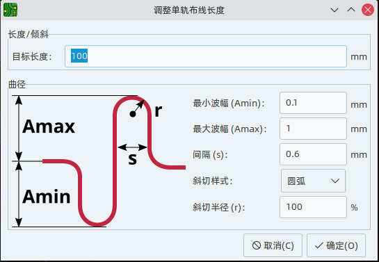
此对话框还可用于配置曲折形状的大小、形状和间距。
配置好目标长度后,在你希望开始放置蛇形形状的区域点击一个布线。 沿着线段移动鼠标光标,蛇形形状就会被添加。 光标旁边会出现一个状态窗口,显示布线的当前长度和目标长度。 再次点击,完成放置当前的蛇形布线。 如果需要,可以在同一条布线上放置多条蛇形布线。
| 长度调整工具仅支持调整两个焊盘之间的点对点网络的长度。尚不支持调整具有不同拓扑的网络长度。 |
交互式布线设置
交互式布线器设置可通过路径菜单访问,或通过右键单击工具栏中的布线按钮来访问。这些设置控制布线和拖动现有布线时的布线行为。
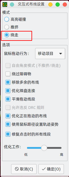
| 设置 | 说明 |
|---|---|
模式 |
设置用于创建新布线和拖动现有布线的路由器的操作模式。 有关详细信息,请参阅上面的内容。 |
自由角度模式 |
允许以任何角度布线,而不是仅以 45 度增量布线。 仅当布线模式设置为突出显示高亮冲突时, 此选项才可用。 |
绕过障碍物 |
在推挤模式下,允许布线尝试在实心障碍物 (如焊盘) 后面移动碰撞布线。 |
移除多余的布线 |
自动删除在当前布线中创建的回路, 仅保留回路中最近布线的部分。 |
优化焊盘连接 |
启用此设置时,交互式布线器尝试在退出焊盘和过孔时避免锐角 和其他不需要的布线。 |
平滑拖动线段 |
拖动布线时,会尝试将布线段组合在一起, 以最大限度地减少方向更改。 |
允许违反 DRC 规则 |
在高亮碰撞模式下,允许放置违反 DRC 规则的布线和过孔。 在其他模式下不起作用。 |
优化正在拖动的布线 |
启用后,拖动布线段将导致 KiCad 优化屏幕上可见的其余布线。 优化过程去除了不必要的拐角,避免了锐角,通常会尝试找到布线的最短路径。 禁用时,不会对正在拖动的紧邻部分之外的布线执行任何优化。 在拖动布线时尝试优化布线。 |
使用鼠标路径设置布线形态 |
尝试根据鼠标路径从布线起点位置拾取布线形态。 如果鼠标从开始位置开始主要沿对角线移动,则形态将设置为对角线起点; 如果鼠标主要水平或垂直移动,则形态将设置为垂直起点。 当鼠标离开布线起始位置很远时,形态估计就会被锁定, 并且可以通过移回起始位置来解锁。 |
点击时固定所有线段 |
启用时,在布线时单击将固定已布线的所有布线段的位置, 包括在鼠标光标结束的线段。新的线段将从鼠标光标位置开始。 禁用时,最后一个线段 (在鼠标光标处结束的线段) 将不会固定在适当位置, 可以通过进一步的鼠标移动进行调整。 |
向前和向后批注
从原理图更新 PCB(正向批注)
使用 "从原理图更新 PCB" 工具将设计信息从原理图编辑器同步到电路板编辑器。在原理图编辑器和电路板编辑器中都可以用 工具 → 从原理图更新 PCB(F8)来访问该工具。你也可以使用电路板编辑器顶部工具栏上的 ![]() 图标。这个过程通常被称为正向批注。
图标。这个过程通常被称为正向批注。
| 从原理图更新 PCB 是将设计信息从原理图转移到 PCB 的首选方法。在旧版本的 KiCad 中,相应的过程是将网表从原理图编辑器中导出并导入到电路板编辑器中。现在已经没有必要使用网表文件了。 |
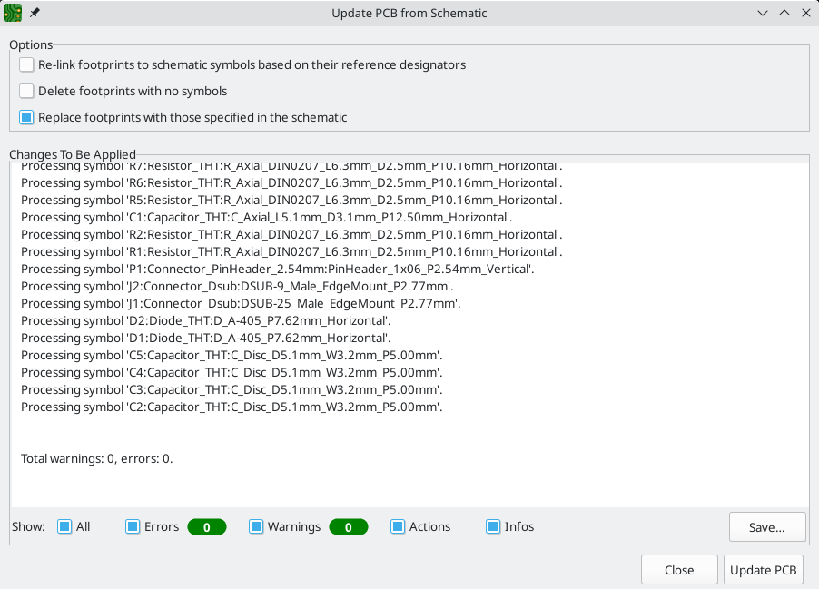
该工具将每个符号的封装添加到电路板上,并将更新的原理图信息传输到电路板上。特别是,电路板的网络连接被更新以符合原理图。
将对 PCB 进行的修改列在 待应用的修改 窗格中。在你点击 更新 PCB 按钮之前,PCB 不会被修改。
你可以使用窗口底部的复选框来显示或隐藏不同类型的信息。可以使用 保存… 按钮将更改的报告保存到文件中。
选项
该工具有几个选项来控制其行为。
| 选项 | 说明 |
|---|---|
根据位号将封装重新链接到原理图符号上 |
封装通常是通过符号添加到原理图中时创建的唯一标识符与原理图符号相连。符号的唯一标识符不能被改变。 如果选中,PCB 中的每个封装将被重新链接到与该封装具有相同位号的符号上。 如果不勾选,封装和符号将像往常一样通过唯一的标识符来链接,而不是通过位号。每个封装的位号将被更新以匹配其链接符号的位号。 这个选项一般不应该被选中。它对依赖改变原理图符号和封装之间的链接的特定工作流程很有用,例如重构原理图以方便布局,或者在设计的相同通道之间复制布局。 |
删除没有符号的封装 |
如果选中,PCB 中任何在原理图中没有相应符号的封装都将从 PCB 中删除。带有 "不在原理图中" 属性的封装将不受影响。 如果不勾选,没有相应符号的封装将不会被删除。 |
用原理图中指定的封装替换封装 |
如果选中,PCB 中的封装将被替换为相应原理图符号中指定的封装。 如果不勾选,即使原理图符号被更新为指定了不同的封装,PCB 中已有的封装也不会被改变。 |
从 PCB 上更新原理图(反向批注)。
KiCad 的典型工作流程是在原理图中进行修改,然后使用 "从原理图更新 PCB" 工具将修改内容同步到电路板上。然而,相反的过程也是可行的:可以在电路板上进行设计修改,然后在原理图或电路板编辑器中使用 工具 → 从 PCB 更新原理图 同步到原理图上。这个过程通常被称为反向批注。
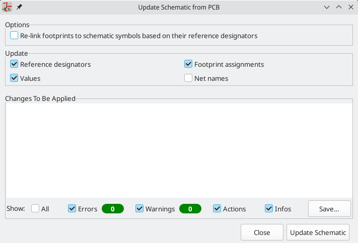
该工具将位号、值、封装分配和网络名称的变化从电路板同步到原理图。每种类型的变化都可以单独启用或禁用。
将对原理图进行的修改列在 待应用的修改 窗格中。在您点击 更新原理图 按钮之前,原理图不会被修改。
你可以使用窗口底部的复选框来显示或隐藏不同类型的信息。可以使用 保存… 按钮将更改的报告保存到文件中。
选项
该工具有几个选项来控制其行为。
选项 |
说明 |
根据位号将封装重新链接到原理图符号上 |
如果选中,PCB 中的每个封装将被重新链接到与该封装具有相同位号的符号上。这个选项与更新符号位号不兼容。 如果不勾选,封装和符号将像往常一样通过唯一的标识符连接,而不是通过位号。 |
位号 |
如果选中,符号位号将被更新,以匹配链接封装的位号。 如果不勾选,符号位号将不会被更新。 |
值 |
如果选中,符号值将被更新以匹配链接封装的值。 如果不勾选,符号值不会被更新。 |
封装分配 |
如果选中,符号的封装分配将被更新,这些符号的封装在电路板中被改变或替换。 如果不勾选,符号的封装分配将不会被更新。 |
网络名 |
如果选中,原理图将根据电路板上的任何网络名变化进行更新。如有必要,网络标签将被更新或添加到原理图中,以便与电路板相匹配。 如果不勾选,原理图中的网络名将不会被更新。 |
| 《全局重新批注,全局重新批注》功能可以与反向批注位号结合使用,根据设计中的位置重新批注所有元件。 |
用 CMP 文件进行反向批注
通过从 PCB 编辑器导出 CMP 文件(文件 → 导出 → 封装关联(.cmp)文件…)并在原理图编辑器中导入(文件 → 导入 → 封装分配…),也可以将选择的变化从 PCB 上同步到原理图。
| 这种方法只能同步对封装分配和封装字段的修改。建议使用 "从 PCB 更新原理图" 工具来代替。 |
位置重新批注
| This section of the KiCad documentation has not yet been written. We appreciate your patience as our small team of volunteer documentation writers work to update and expand the documentation. |
锁定
大多数对象可以通过其属性对话框、右键上下文菜单或使用 "切换锁定" 快捷键(L)来锁定。 被锁定的对象不能被选择,除非选择过滤器中的 "被锁定的项目" 复选框被启用。 试图移动锁定的项目将导致一个警告对话框:
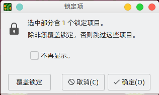
在这个对话框中选择 "覆盖锁定" 将允许移动锁定的项目。 选择 "确定" 将允许你在选择中移动任何未上锁的项目;留下锁定的项目。 选择 "不再显示" 将使你在剩下的会话中记住你的选择。
批量编辑工具
| This section of the KiCad documentation has not yet been written. We appreciate your patience as our small team of volunteer documentation writers work to update and expand the documentation. |
清理工具
| This section of the KiCad documentation has not yet been written. We appreciate your patience as our small team of volunteer documentation writers work to update and expand the documentation. |
正在导入图形
| This section of the KiCad documentation has not yet been written. We appreciate your patience as our small team of volunteer documentation writers work to update and expand the documentation. |
从 DXF 和 SVG 文件导入矢量图
| This section of the KiCad documentation has not yet been written. We appreciate your patience as our small team of volunteer documentation writers work to update and expand the documentation. |
正在导入位图图像
| This section of the KiCad documentation has not yet been written. We appreciate your patience as our small team of volunteer documentation writers work to update and expand the documentation. |