Editing a board
Placement and drawing operations
Placement and drawing tools are located in the right toolbar. When a tool is activated, it stays active until a different tool is selected or the tool is canceled with the Esc key. The selection tool is always activated when any other tool is canceled.
Some toolbar buttons have more than one tool available in a palette. These tools are indicated with a small arrow in the lower-right corner of the button: 
To show the palette, you can click and hold the mouse button on the tool or click and drag the mouse. The palette will show the most recently used tool when it is closed.
|
Selection tool (the default tool). |
|
Local ratsnest tool: when the board ratsnest is hidden, selecting footprints with this tool will show the ratsnest for the selected footprint only. Selecting the same footprint again will hide its ratsnest. The local ratsnest setting for each footprint will remain in effect even after the local ratsnest tool is no longer active. |
|
Footprint placement tool: click on the board to open the footprint chooser, then click again after choosing a footprint to confirm its location. |
|
Route tracks / route differential pairs: These tools activate the interactive router and allow placing tracks and vias. The interactive router is described in more detail in the Routing Tracks section below. |
|
Tune length: These tools allow you to tune the length of single tracks or the length or skew of differential pairs, after they have been routed. See the Routing Tracks section for details. |
|
Add vias: allows placing vias without routing tracks. Vias placed on top of tracks using this tool will take on the net of the closest track segment and will become part of that track (the via net will be updated if the pads connected to the tracks are updated). Vias placed anywhere else will take on the net of a copper zone at that location, if one exists. These vias will not automatically take on a new net if the net of the copper zone is changed. |
|
Add filled zone: Click to set the start point of a zone, then configure its properties before drawing the rest of the zone outline. Zone properties are described in more detail below. |
|
Add rule area: Rule areas, formerly known as keepouts, can restrict the placement of items and the filling of zones and can also define named areas to apply specific custom design rules to. |
|
Draw lines. Note: Lines are graphical objects and are not the same as tracks placed with the Route Tracks tool. Graphical objects cannot be assigned to a net. |
|
Draw arcs: pick the center point of the arc, then the start and end points. By right clicking this button, you can change the arc editing mode between a mode that maintains the existing arc center and a mode that maintains the arc radius. |
|
Draw rectangles. Rectangles can be filled or outlines. |
|
Draw circles. Circles can be filled or outlines. |
|
Draw graphical polygons. Polygons can be filled or outlined. Note: Filled graphical polygons are not the same as filled zones: graphical polygons cannot be assigned to a net and will not keep clearance from other items. |
|
Add bitmap image. |
|
Add text. |
|
Add a textbox. |
|
Add dimensions. Dimension types are described in more detail below. |
|
Deletion tool: click objects to delete them. |
|
Set drill/place origin (used for fabrication outputs) or grid origin. |
|
Interactively measure the distance between two points. |
Snapping
When moving, dragging, and drawing board elements, the grid, pads, and other elements can have snapping points depending upon the settings in the user preferences. In complex designs, snap points can be so close together that it makes the current tool action difficult. Both grid and object snapping can be disabled while moving the mouse by using the modifier keys in the table below.
| Modifier Key | Effect |
|---|---|
Ctrl |
Disable grid snapping. |
Shift |
Disable object snapping. |
Editing object properties
All objects have properties that are editable in a dialog. Use the hotkey E or select Properties from the right-click context menu to edit the properties of selected item(s). You can only open the properties dialog if all the items you have selected are of the same type. To edit the properties of different types of items at one time, see the section below on bulk editing tools.
In properties dialogs, any field that contains a numeric value can also accept a basic math expression that results in a numeric value. For example, a dimension may be entered as 2 * 2mm, resulting in a value of 4mm. Basic arithmetic operators as well as parentheses for defining order of operations are supported.
Working with footprints
Adding footprints to the board
Footprints are automatically added to the board when the PCB is updated from the schematic. The footprint associated with each schematic symbol is added to the board if it is not already present, and each footprint pad is associated with the corresponding symbol pin’s net. Symbol pins are matched to footprint pads by pin/pad number.
When footprints are added to the board after an update from the schematic, they are grouped by schematic sheet and by geographical location in the schematic. They are initially attached to the cursor; you can place them by clicking in the desired location.
You can also add footprints to the board manually using the Add Footprint tool (A or the ![]() button). Note that footprints added in this way will not be automatically associated with a symbol or have nets assigned to their pads, and subsequent updates from the schematic will remove these unassociated footprints unless the footprint is locked or the Delete footprints with no symbols option is unchecked in the Update PCB From Schematic dialog. For these reasons, it is usually recommended to avoid manually adding footprints to the board. Manually adding footprints is necessary for PCB-only workflows, and can also be useful for adding logos or other footprints that do not need a corresponding schematic symbol.
button). Note that footprints added in this way will not be automatically associated with a symbol or have nets assigned to their pads, and subsequent updates from the schematic will remove these unassociated footprints unless the footprint is locked or the Delete footprints with no symbols option is unchecked in the Update PCB From Schematic dialog. For these reasons, it is usually recommended to avoid manually adding footprints to the board. Manually adding footprints is necessary for PCB-only workflows, and can also be useful for adding logos or other footprints that do not need a corresponding schematic symbol.
Placing and moving footprints
Once footprints have been added to the board, you can reposition them in many ways.
The Move command (M) moves a footprint or a selection of footprints, ignoring any connected track segments that are not selected. No DRC checking is done when moving footprints with the Move command.
There is a reference point for the move operation, which is the point in the footprint which attaches to the cursor and therefore the point in the footprint that snaps to the grid and to other objects. The reference point during a move is determined by the location of the cursor when the Move command is initiated. If the cursor is over a pad, the pad’s center will be used as the reference point. If the cursor is not over a pad, the footprint’s anchor (coordinate origin point) will be used. To select an arbitrary snapping point, you can use the Move With Reference command instead of the regular Move command (right click → Positioning Tools → Move with Reference). After initiating the command, click on the desired reference point; KiCad will then begin the move with that point as the reference.
You can also use the Drag command (D) to move the selected footprint using the interactive router, maintaining all track connections to the footprint. Dragging footprints behaves like the Highlight Collisions router mode: obstacles will not be avoided or shoved, only highlighted. Only one footprint at a time can be dragged.
Flip a footprint to the opposite side of the board with the F hotkey. Any parts of the footprint on a front layer will be swapped to the corresponding back layer, and vice versa.
Rotate a footprint counter-clockwise using the R hotkey, or clockwise using Shift+R. By default, footprints are rotated by 90 degrees every time the rotate command is used, but you can configure the rotation angle step in Preferences → PCB Editor → Editing Options.
You can directly set a footprint’s exact absolute position, rotation angle, and PCB side using either the Footprint Properties dialog or the Properties panel.
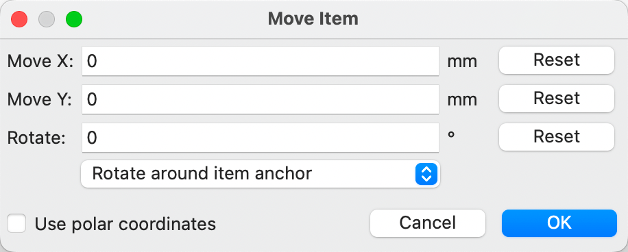
To reposition a footprint relative to its current position, use the Move Exactly tool (Shift+M). The dialog lets you specify an X and Y translation, as well as a rotation, that will be applied to the footprint. The rotation can be performed relative to either the footprint’s anchor, the local coordinate origin, or the drill/place origin. You can also use polar coordinates instead of Cartesian coordinates.
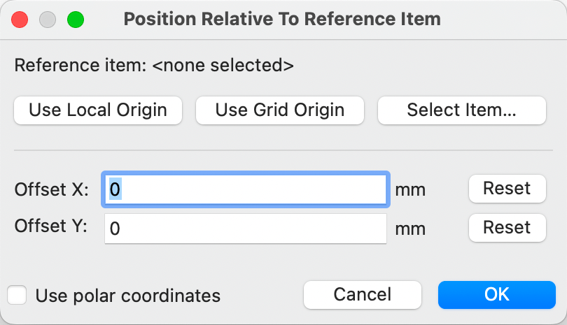
To position a footprint relative to another object, you can use the Position Relative tool (Shift+P). With this tool, you select a reference point for the move, which can be the local origin, the grid origin, or another arbitrary point, such as a pad in another footprint. The selected footprint is moved to the specified offset from the reference point.
You can swap the position of two selected footprints using the Swap command (Shift+S). The first footprint is assigned the location, rotation, and board side of the second footprint, and vice versa. If there are more than two footprints selected, the locations are cycled: the last footprint gets the position of the first footprint, the first footprint gets the location of the second, and so on.
There are several convenience features that make it easier to find, select, and move specific footprints or footprints related to another footprint.
The Get and Move Footprint command (T) prompts you to choose a footprint from a list or by typing a reference designator. KiCad then attaches the chosen footprint to your cursor for a move operation.
There are two commands to select other footprints that need to be connected to the selected footprint but don’t yet have routed connections. The Select All Unconnected Footprints command (O) selects all footprints that have ratsnest lines to the currently selected footprints. The command can be executed repeatedly to further expand the selection based on the newly selected items. The Grab Nearest Unconnected Footprint command (Shift+O) selects the closest footprint with ratsnest lines to the currently selected footprint, and additionally begins to move it. If there are multiple footprints initially selected, the command will act like the Move Individually command described below, individually moving the closest unconnected footprint for each of the initially selected footprints.
You can select footprints based on their schematic sheet using the right click → Select → Items in Same Hierarchical Sheet command, which selects all other footprints that are in the same schematic sheet as the originally selected footprint.
If you want to move multiple selected footprints in sequence, use the Move Individually command (Ctrl+M). After triggering the command, KiCad will begin moving the first selected footprint. After you click to place the footprint, KiCad will immediately start moving the next footprint, in the same order that you selected the footprints. You can skip moving a footprint by pressing Tab, commit the current move and skip any remaining moves by double-clicking, or cancel all moves (including those already completed) by pressing Esc.
If you want to move a collection of footprints at once into one area, the Pack and Move Footprints command (P) closely packs the selected footprints together and moves them as a block.
| Move Individually and Pack and Move Footprints are useful in combination with other selection convenience features, such as cross-selection from the schematic or the advanced footprint selection features described above. For example, you could select a group of bypass capacitors in the Schematic Editor, switch to the PCB Editor where the corresponding footprints are now selected, and then use Move Individually to quickly place all of the bypass capacitor footprints close to their respective ICs. Alternatively, you could use one of the other selection tools, such as Select All Unconnected Footprints, to select many footprints from all over the board, then use Pack and Move Footprints to quickly put them all into a small area. |
Finally, KiCad can automatically place footprints onto the board. The auto-place function attempts to optimally place footprints to simplify ratsnest connections to other footprints. You can auto-place the selected footprints with Place → Auto-Place Footprints → Place Selected Footprints, or auto-place all footprints outside of the board outline with Place → Auto-Place Footprints → Place Off-Board Footprints.
Proprietà impronte
| This section of the KiCad documentation has not yet been written. We appreciate your patience as our small team of volunteer documentation writers work to update and expand the documentation. |
Editing Footprints
| This section of the KiCad documentation has not yet been written. We appreciate your patience as our small team of volunteer documentation writers work to update and expand the documentation. |
Working with pads
The properties of each individual pad of a footprint can be inspected and edited after placing the footprint on the board. In other words, it is possible to override the design of an individual footprint pad in a specific instance of the footprint on the board, if the footprint design in the library is not appropriate. For example, you may wish to remove the solder paste aperture for a pad that needs to remain unsoldered in a specific design, or you may wish to move the location of a through-hole pad for an axial-lead resistor in order to fit a specific design.
| By default, the position of all footprint pads are locked, so it is possible to edit the pad properties but not move the pad’s location relative to the rest of the footprint. Pads may be unlocked to allow free movement, which can be useful for certain applications (such as through-hole footprints with varying lead positions) but is generally never recommended for surface-mount footprints. |
The pad properties dialog is opened through the context menu or default hotkey E when a pad is selected. Note that KiCad assumes that if you click near a pad, you are probably trying to select the entire footprint rather than a single pad. To select a single pad, make sure to click inside the pad area, or turn off the Footprints setting in the selection filter (and make sure the Pads setting is turned on) to prevent accidental selection of the entire footprint rather than a specific pad.
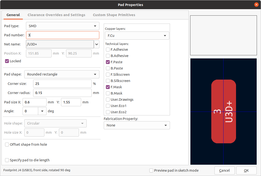
The General tab of the pad properties dialog shows the physical properties of the pad, including its geometry, shape, and layer settings.
Pad type: this setting controls which features are enabled for the pad:
SMD pads are electrically-connected and have no hole. In other words, they exist on a single copper layer.
Through-hole pads are electrically-connected and have a plated hole. The hole exists on every layer, and the copper pad exists on multiple layers (see Copper layers setting below).
Edge Connector pads are SMD pads that are allowed to overlap the board outline on the Edge.Cuts layer.
NPTH, Mechanical pads are non-plated through holes that do not have an electrical connection.
SMD Aperture pads are pads that have no hole and no electrical connection. These can be used to add specific designs to a technical layer, for example a paste or solder mask aperture.
The Copper layers setting controls which copper layers will have a shape associated with the pad.
For SMD pads, the options are F.Cu or B.Cu, controlling whether the pad sits on the front or the back of the board relative to the footprint’s location. In other words, if a pad is set to exist on B.Cu in its properties, and the footprint is flipped to the back of the board, that pad will now exist on F.Cu, because it also has been flipped.
For through-hole pads, it is possible to remove the pad shape from copper layers where the pad is not electrically connected to other copper (tracks or filled zones). Setting the copper layers to connected layers only will remove the pad shape from any unconnected layers, and setting to F.Cu, B.Cu, and connected layers will remove the pad shape from any internal unconnected layers. This can be useful in dense board designs to increase the routable area on internal layers.
The Technical layers checkboxes control which technical layers will have an aperture added with the pad’s shape. By default, pads have apertures on the paste and mask layers matching their copper layer.
| It is not possible to define a different pad shape or size on different copper layers in the current version of KiCad. |
Specify pad to die length: This setting allows a length to be associated with this pad that will be added to the routed track length by the track length tuning tools and the Net Inspector. This can be used to specify internal bondwire lengths for more accurate length matching, or in other situations where the electrical length of a net is longer than the length of the routed tracks on the board.
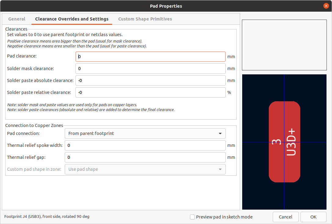
The aperture appearing on any technical layer will have the same shape and size as the pad shape on the copper layer(s). In the PCB manufacturing process, the manufacturer will often change the relative size of mask and paste apertures relative to the copper pad size, but since this size change is specific to a manufacturing process, most manufacturers expect the design data to be provided with the apertures set to the same size as the copper pads. For specific situations where you need to oversize or undersize a technical layer aperture in the design data, you can use the settings in the Overrides tab.
Pad clearance controls the minimum clearance between the pad and any copper shape (tracks,
vias, pads, zones) on a different net. This value is normally set to 0 which will cause the pad
clearance to be inherited from any clearance override set on the footprint, or the board’s design
rules and netclass rules if the footprint clearance is also set to 0.
Solder mask clearance controls the size difference between the pad shape and the aperture shape
on the F.Mask and B.Mask layers. A positive number means the solder mask aperture will be larger
than the copper shape. This number is an inflation applied to all directions. For example, a
value of 0.1mm here will cause the solder mask aperture to be inflated by 0.1mm, meaning that
there will be an 0.1mm border on all sides of the pad and the solder mask opening will be 0.2mm
wider than the pad when measured along a given axis.
Solder paste absolute clearance controls the size difference between the pad shape and the aperture shape on the F.Paste and B.Paste layers. Its behavior is otherwise identical to the behavior of the solder mask clearance setting.
Solder paste relative clearance allows setting a solder paste clearance value as a percentage of the pad size rather than an absolute distance value. If both relative and absolute clearances are specified, they are added together to determine the solder paste aperture size.
The Overrides tab also has controls for how the pad connects to any copper zone that overlaps it and shares its net.
Pad connection controls whether the pad will have a solid, thermal relief, or no connection to the zone. Like the other overrides, this one may be set for an individual pad or for an entire footprint. The default setting for this control is From parent footprint, and the default footprint setting is to use the connection mode specified in the zone properties.
Thermal relief spoke width controls the width of the spokes generated when the zone connection mode is Thermal Relief.
Thermal relief gap controls the length of the thermal spokes, or the gap between the pad’s shape and the filled copper area of the zone.
Custom pad shape in zone controls the behavior of the zone filler when the pad uses a custom shape rather than one of the default shapes. This can be used to achieve different results when using thermal reliefs and custom pad shapes.
Working with zones
Copper zones, also sometimes called copper pours or fills by other EDA tools, are solid or hatched areas of copper assigned to a particular net that automatically keep clearance from other copper objects. Zones are commonly used to fill in all free space on a board layer (or a portion of a layer) in order to create ground and power planes, carry high currents, or to provide shielding.
| Some EDA tools have separate tools for creating "plane layers" and for creating copper zones on signal layers. In KiCad, the Copper Zone tool is used for both these applications. |
Zones are defined by a polygonal outline that defines the maximum extent of the filled copper area. This outline does not represent physical copper and will not appear in exported manufacturing data. The actual copper areas of the zone must be filled each time the outline, or any objects inside the outline, are modified. The filling process may be run on a single zone, or on all zones in a board (default hotkey B). Zones may be unfilled (default hotkey Ctrl+B) to improve performance and reduce visual clutter while editing large boards.
| By default, zone filling is a manual process rather than occurring every time an object changes that would result in a change to the zone copper. This is because zone filling can be a slow process on older computers or very large designs. It is important to make sure zone fills are up-to-date before generating outputs. KiCad will check that zones have been updated and warn you before generating outputs or running DRC when zones have not yet been refilled. You can optionally enable automatic zone-filling in the Preferences dialog (PCB Editor → Editing Options → Miscellaneous → Auto-refill zones). |
To draw a zone, click the Add Filled Zone tool (![]() ) on the right toolbar, or use default hotkey Ctrl+Shift+Z. Click to choose the first point of the zone outline. The Zone Properties dialog will appear, allowing you to choose the zone net and other properties. These properties may be edited at any time, so it is not critical to choose them all correctly at first. Accept the dialog and continue placing points to define the zone outline. To finish the zone, double-click to set the last point. Zone outline points may be modified like graphic polygons, by dragging the square handles to move a corner or dragging the circular handles to move an edge. To edit the zone’s properties, use hotkey E or select Properties from the context menu.
) on the right toolbar, or use default hotkey Ctrl+Shift+Z. Click to choose the first point of the zone outline. The Zone Properties dialog will appear, allowing you to choose the zone net and other properties. These properties may be edited at any time, so it is not critical to choose them all correctly at first. Accept the dialog and continue placing points to define the zone outline. To finish the zone, double-click to set the last point. Zone outline points may be modified like graphic polygons, by dragging the square handles to move a corner or dragging the circular handles to move an edge. To edit the zone’s properties, use hotkey E or select Properties from the context menu.
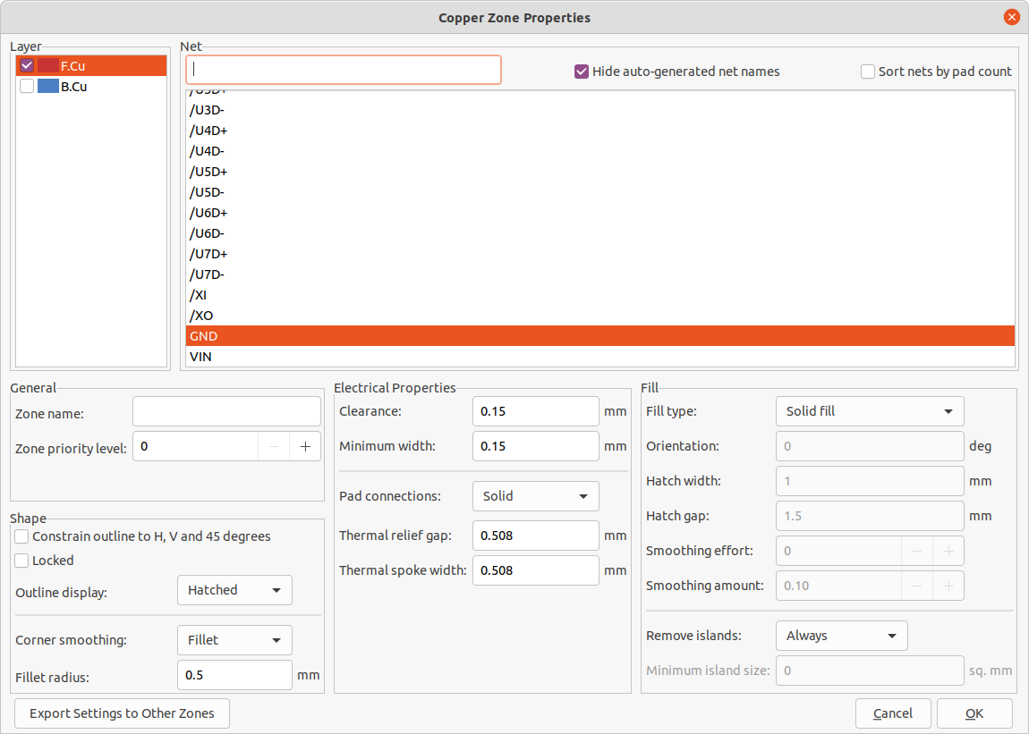
Layer: A single zone object can create filled copper on one or more copper layers. Check the box next to each copper layer that this zone outline should fill on. The copper on each layer will be filled independently, but all layers will share the same net.
Net: Select the electrical net that the zone copper should be connected to. It is possible to create zones with no net assignment. Zones with no net will keep clearance from any copper objects on any net.
Zone name can be used to assign a specific name to a zone. This name can be used to refer to the zone in custom DRC rules.
Zone priority level determines the order in which multiple zones on a single layer are filled. The highest priority level zone on a given layer will be filled first. Lower-priority zones will keep clearance to the filled areas of higher-priority zones. Two zones on the same layer with the same priority level will overlap (short-circuit) with each other, unless they are assigned different nets. When two zone outlines with the same priority and different nets touch, one zone will maintain clearance to the other so that they don’t short.
Constrain outline to H, V and 45 degrees controls the initial behavior of the zone outline drawing tool. When this option is enabled, the zone outline will be restricted to 45-degree angles. Note that after the zone outline has been created, this option has no effect. Outline points may be modified freely after creation.
Locked controls whether or not the zone outline object is locked. Locked objects may not be manipulated or moved, and cannot be selected unless the Locked Items option is enabled in the Selection Filter panel.
Outline display controls how the zone outline is drawn on screen. In Line mode, only the border lines of the outline are drawn. In Hatched mode, hatch lines are drawn on the inside of the outline border for a short distance, to make the zone outline more apparent. In Fully Hatched mode, hatch lines are drawn across the entire inside of the zone outline.
Corner smoothing controls the behavior of the filled copper areas at corners of the outline. Corners can be smoothed by a chamfer or fillet, or can extend all the way to the outline corner if smoothing is disabled.
| By default, chamfers and fillets are not added to inside corners of the zone outline, because this would result in filled copper extending outside the outline. If smooth inside corners are desired, enable the Allow fillets outside zone outline option in the Constraints section of the Board Setup dialog. |
Clearance controls the minimum clearance the filled areas of this zone will keep from other copper objects. Note that if two clearance values are in conflict, the larger clearance value will be used. For example, if a zone is set to use 0.2mm clearance but its netclass is set to use 0.3mm clearance, the result will be an 0.3mm clearance.
Minimum width controls the minimum size of narrow necks of copper created inside the zone. Any copper areas that would be below this minimum width are removed during the filling process.
Pad connection controls the way that the filled zone areas will connect to footprint pads on the same net. Solid connections will result in the copper completely overlapping the pads. Thermal reliefs will result in small copper spokes connecting the pad to the rest of the copper zone, increasing the thermal resistance between the pad and the rest of the zone. This can be useful for hand soldering. Reliefs for PTH will apply thermal reliefs to plated through-hole pads and use solid connections for surface mount pads. None will result in the zone not connecting to any pads on the same net.
Thermal relief gap controls the distance maintained between any pad and the copper zone when the pad connection mode is set to generate thermal reliefs.
Thermal spoke width controls the width of the "spokes", or short copper segments connecting the pad to the rest of the copper zone.
Fill type controls how the copper zone is filled: the default is solid fill, which will result in copper filling in all available space within the zone outline. The zone can also be set to fill a hatch pattern, which will fill the area with a pattern that contains less copper. This can be useful for flexible printed circuits and other specialty applications.
Orientation controls the angle of the hatch pattern lines. An orientation of 0 degrees will result in the hatch pattern using horizontal and vertical lines.
Hatch width controls the width of each line in the hatch pattern.
Hatch gap controls the distance between each line in the hatch pattern.
Smoothing effort controls the style of smoothing applied to the hatch pattern. A value of 0 will result in no smoothing, and a value of 3 will result in the finest smoothing. Higher values will result in longer processing time and larger Gerber files.
Smoothing amount is a ratio that controls the size of the smoothing chamfers or fillets that are generated when smoothing effort is set to a value other than 0. An amount of 0.0 results in no smoothing, and a value of 1.0 results in maximum smoothing (in other words, a chamfer or fillet equal to half of the hatch gap).
Remove islands controls the behavior of isolated copper areas, also called islands, after the initial zone fill. When this is set to always, isolated areas inside the zone are removed. When set to never, isolated areas are left alone, and will result in copper areas that are not connected to the rest of the net. When set to below area limit, a minimum island size can be specified, and islands below this threshold will be removed.
| Regardless of the remove islands setting, islands are never removed from zones that are electrically unconnected. In other words, islands are only removed from zones that have at least one electrical connection. |
Graphical objects
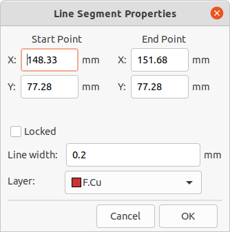
Graphical objects (lines, arcs, rectangles, circles, polygons, and text) can exist on any layer but cannot be assigned to a net. Rectangles, circles, and polygons can be set to be filled or outlines in their properties dialogs. The line width property will control the width of the outline even for filled shapes. Line width can be set to 0 for filled shapes to disable the outline.
Creating graphical shapes
The right toolbar can be used to create lines (![]() , default hotkey Ctrl+Shift+L), arcs (
, default hotkey Ctrl+Shift+L), arcs (![]() , default hotkey Ctrl+Shift+A), rectangles (
, default hotkey Ctrl+Shift+A), rectangles (![]() ), circles (
), circles (![]() , default hotkey Ctrl+Shift+C), and polygons (
, default hotkey Ctrl+Shift+C), and polygons (![]() , default hotkey Ctrl+Shift+P).
, default hotkey Ctrl+Shift+P).
Rectangles, circles, and polygons can be filled shapes or outlines. The line width option controls the width of the outline. The outline width extends on both sides of the "ideal" shape of the graphic object. For example, a graphic circle that is defined to have 2mm radius and 0.2mm line width will consist of a torus with an outer radius of 2.2mm and inner radius of 1.8mm. If the filled shape option is enabled and the line width is set to 0, the shape will be a filled circle with 2mm radius.
Arcs have two editing modes, which are selectable in Preferences → PCB Editor → Editing Options or by right clicking the ![]() button on the right toolbar. The first mode (keep arc center, adjust radius) maintains the position of the arc center as as the arc endpoints or midpoint are dragged, changing the radius as necessary. The second mode (keep arc endpoints or direction of starting point) maintains the position of the arc endpoints and the arc’s direction of curvature as the midpoint or center are dragged.
button on the right toolbar. The first mode (keep arc center, adjust radius) maintains the position of the arc center as as the arc endpoints or midpoint are dragged, changing the radius as necessary. The second mode (keep arc endpoints or direction of starting point) maintains the position of the arc endpoints and the arc’s direction of curvature as the midpoint or center are dragged.
Creating text objects
Graphical text may be placed by using the (![]() ) icon in the right toolbar or by keyboard shortcut Ctrl+Shift+T. Click to place the text origin, and then edit the text and its properties in the dialog that will appear:
) icon in the right toolbar or by keyboard shortcut Ctrl+Shift+T. Click to place the text origin, and then edit the text and its properties in the dialog that will appear:
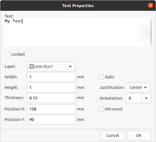
Text may be placed on any layer, but note that text on copper layers cannot be associated with a net and cannot form connections to tracks or pads. Copper zones will fill around the rectangular bounding box of text objects.
Text supports markup for superscripts, subscripts, overbars, evaluating project variables, and accessing symbol field values.
| Feature | Markup Syntax | Result |
|---|---|---|
Superscript |
|
textsuperscript |
Subscript |
|
textsubscript |
Overbar |
|
text |
|
variable_value |
|
|
field_value of symbol refdes |
| Variables must be defined in Board Setup before they can be used. There are also a number of built-in text variables. |
Board outlines (Edge Cuts)
KiCad uses graphical objects on the Edge.Cuts layer to define the board outline. The outline must be a continuous (closed) shape, but can be made up of different types of graphical object such as lines and arcs, or be a single object such as a rectangle or polygon. If no board outline is defined, or the board outline is invalid, some functions such as the 3D viewer and some design rule checks will not be functional.
Bulk editing text and graphics
Properties of text and graphics can be edited in bulk using the Edit Text and Graphic Properties dialog (Tools → Edit Text and Graphic Properties…).
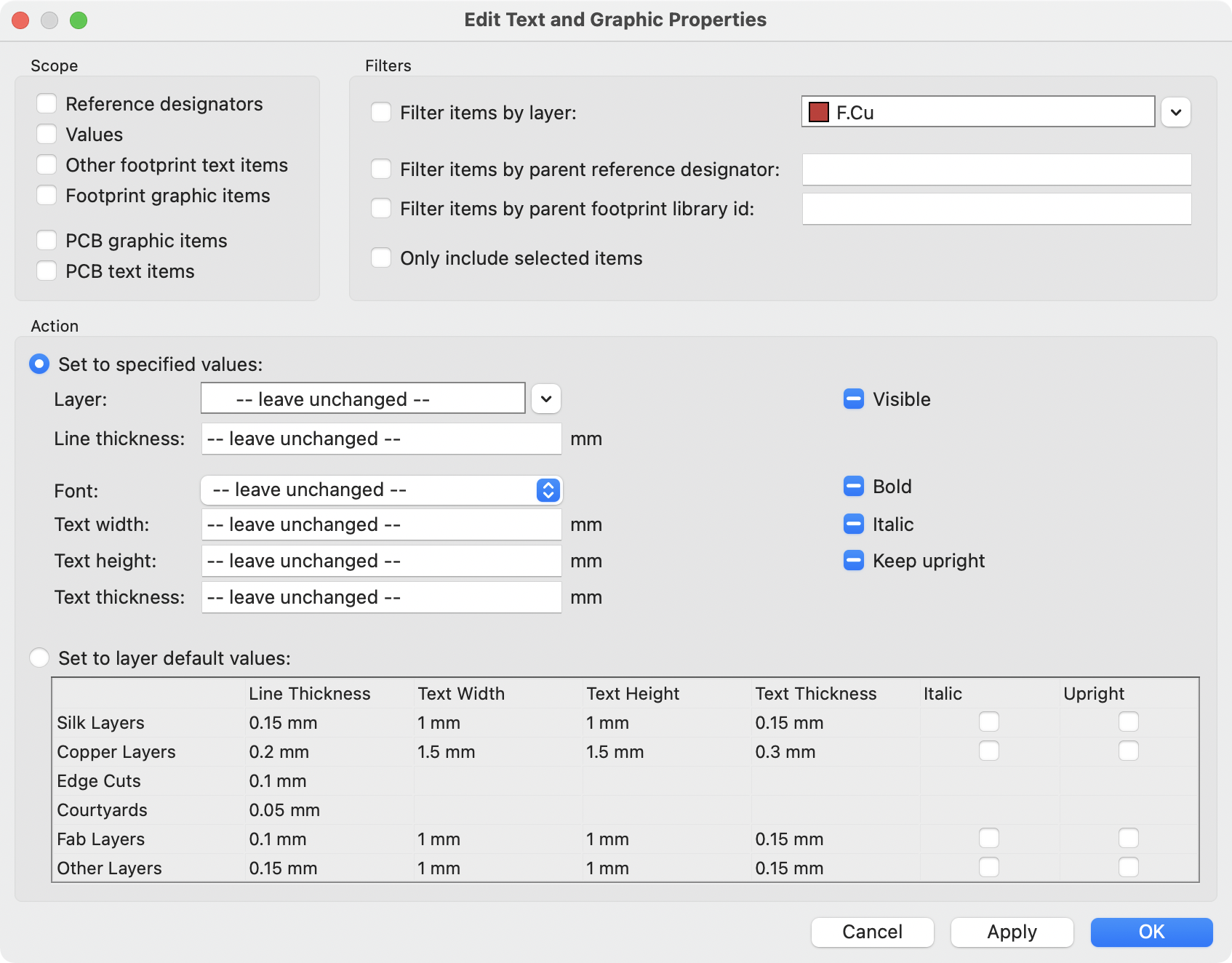
Scope and Filters
Scope settings restrict the tool to editing only certain types of objects. If no scopes are selected, nothing will be edited.
Filters restrict the tool to editing particular objects in the selected scope.
Objects will only be modified if they match all enabled and relevant filters
(some filters do not apply to certain types of objects. For example, parent
footprint filters do not apply to graphic items and are ignored for the purpose
of changing graphic properties). If no filters are enabled, all objects in the
selected scope will be modified. For filters with a text box, wildcards are
supported: * matches any characters, and ? matches any single character.
Filter items by layer filters to items on the specified board layer.
Filter other symbol fields by name filters to the specified symbol field.
Filter items by parent reference designator filters to fields in the footprint with the specified reference designator. Filter items by parent footprint library id filters to fields in footprint with the specified library identifier.
Only include selected items filters to the current selection.
Action
Properties for filtered objects can be set to new values in the bottom part of the dialog. Properties can be set to arbitrary values by selecting set to specified values or reset to their layer’s default value by selecting set to layer default values.
Drop-down lists and text boxes can be set to -- leave unchanged -- to preserve existing values. Checkboxes can be checked or unchecked to enable or disable a change, but can also be toggled to a third "leave unchanged" state.
All items can have their layer set.
Graphic items can have their line thickness modified.
Text properties that can be modified are font, text width, text height, text thickness (KiCad font only), emphasis (bold and italic), and orientation (keep upright). Footprint text can also have its visibility set.
Dimensions
Dimensions are graphical objects used to show a measurement or other marking on a board design. They may be added on any drawing layer, but are normally added to one of the User layers. KiCad currently supports five different types of dimension: aligned, orthogonal, center, radial, and leader.
Aligned dimensions (![]() ) show a measurement of
distance between two points. The measurement axis is the line that connects those two points, and
the dimension graphics are kept parallel to that axis.
) show a measurement of
distance between two points. The measurement axis is the line that connects those two points, and
the dimension graphics are kept parallel to that axis.
Orthogonal dimensions (![]() ) also measure the
distance between two points, but the measurement axis is either the X or Y axis. In other words,
these dimensions show the horizontal or vertical component of the distance between two points.
When creating orthogonal dimensions, you can select which axis to use as the measurement axis based
on where you place the dimension after selecting the two points to measure.
) also measure the
distance between two points, but the measurement axis is either the X or Y axis. In other words,
these dimensions show the horizontal or vertical component of the distance between two points.
When creating orthogonal dimensions, you can select which axis to use as the measurement axis based
on where you place the dimension after selecting the two points to measure.
Center dimensions (![]() ) create a cross mark to
indicate a point or the center of a circle or arc.
) create a cross mark to
indicate a point or the center of a circle or arc.
Radial dimensions (![]() ) show a measurement between
a center point and the outside of a circle or arc. The center point is indicated by a cross.
) show a measurement between
a center point and the outside of a circle or arc. The center point is indicated by a cross.
Leader dimensions (![]() ) create an arrow with a leader line
connected to a text field. This text field can contain any text, and an optional circular or
rectangular frame around the text. This type of dimension is often used to call attention to parts
of the design for reference in fabrication notes.
) create an arrow with a leader line
connected to a text field. This text field can contain any text, and an optional circular or
rectangular frame around the text. This type of dimension is often used to call attention to parts
of the design for reference in fabrication notes.
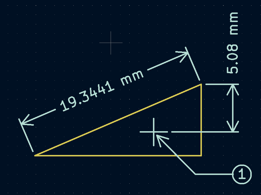
After creating a dimension, its properties may be edited (hotkey E) to change the format of the displayed number and the style of the text and graphic lines.
| You may customize the default style of newly-created dimension objects in the Text & Graphics Defaults section of the Board Setup dialog. |
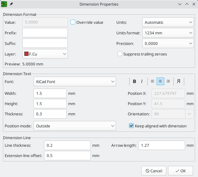
Dimension format options
Override value: When enabled, you may enter a measurement value directly into the Value field that will be used instead of the actual measured value.
Prefix: Any text entered here will be shown before the measurement value.
Suffix: Any text entered here will be shown after the measurement value.
Layer: Selects which layer the dimension object exists on.
Units: Selects which units to display the measured value in. Automatic units will result in the dimension units changing when the display units of the board editor are changed.
Units format: Select from several built-in styles of unit display.
Precision: Select how many digits of precision to display.
Dimension text options
Most of the dimension text options are identical to those options available for other graphical text objects (see the Graphical Objects section above). Some specific options for dimension text are also available:
Position mode: Choose whether to position the dimension text manually, or to automatically keep it aligned with the dimension measurement lines.
Keep aligned with dimension: When enabled, the orientation of the dimension text will be adjusted automatically to keep the text parallel with the measurement axis.
Dimension line options
Line thickness: Sets the thickness of the graphical lines that make up a dimension’s shape.
Extension line offset: Sets the distance from the measurement point to the start of the extension lines.
Arrow length: Sets the length of the arrow segments of the dimension’s shape.
Leader options
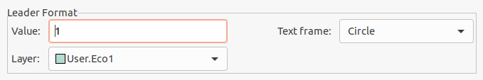
Value: Enter the text to show at the end of the leader line.
Text frame: Select the desired border around the text (circle, rectangle, or none).
Routing tracks
KiCad features an interactive router that:
-
Allows manual or guided (semi-automatic) routing of single tracks and differential pairs
-
Enables modifications of existing designs by:
-
Re-routing existing tracks when they are dragged
-
Re-routing tracks attached to footprint pads when the footprint is dragged
-
-
Allows tuning of track lengths and differential pair skew (phase) by inserting serpentine
tuning shapes for designs with tight timing requirements
By default, the router respects the configured design rules when placing tracks: the size (width) of new tracks will be taken from the design rules and the router will respect the copper clearance set in the design rules when determining where new tracks and vias can be placed. It is possible to disable this behavior if desired by using the Highlight Collisions router mode and turning on the Allow DRC Violations option in the router settings (see below).
The router has three modes that can be selected at any time. The router mode is used for routing new tracks, but also when dragging existing tracks using the Drag (hotkey D) command. These modes are:
-
Highlight Collisions: in this mode, most of the router features are disabled and routing is fully manual. When routing, collisions (clearance violations) will be highlighted in green and the newly-routed tracks cannot be fixed in place if there is a collision unless the Allow DRC Violations option is turned on. In this mode, up to two track segments may be placed at a time (for example, one horizontal and one diagonal segment).
-
Shove: in this mode, the track being routed will walk around obstacles that cannot be moved (for example, pads and locked tracks/vias) and shove obstacles that can be moved out of the way. The router prevents DRC violations in this mode: if there is no way to route to the cursor position that does not violate DRC, no new tracks will be created.
-
Walk Around: in this mode, the router behaves the same as in Shove mode, except no obstacles will be moved out of the way.
Which mode to use is a matter of preference. For most users, we recommend using Shove mode for the most efficient routing experience or Walk Around mode if you do not want the router to modify tracks that are not being routed. Note that Shove and Walk Around modes always create horizontal, vertical, and 45-degree (H/V/45) track segments. If you need to route tracks with angles other than H/V/45, you must use Highlight Collisions mode and enable the Free Angle Mode option in the Interactive Router Settings dialog.
There are five main routing functions: Route Single Track, Route Differential Pair, Tune length of a single track, Tune length of a differential pair, and Tune skew of a differential pair. All of these are present in both the Route menu dropdown (individually) on the top toolbar and the drawing toolbar in two overloaded icons on the drawing toolbar on the right. The use of the overloaded icons is described above. One is for the two Route functions and one is for the three Tune functions. In addition, the Route menu allows the selection of Set Layer Pair and Interactive Router Settings.
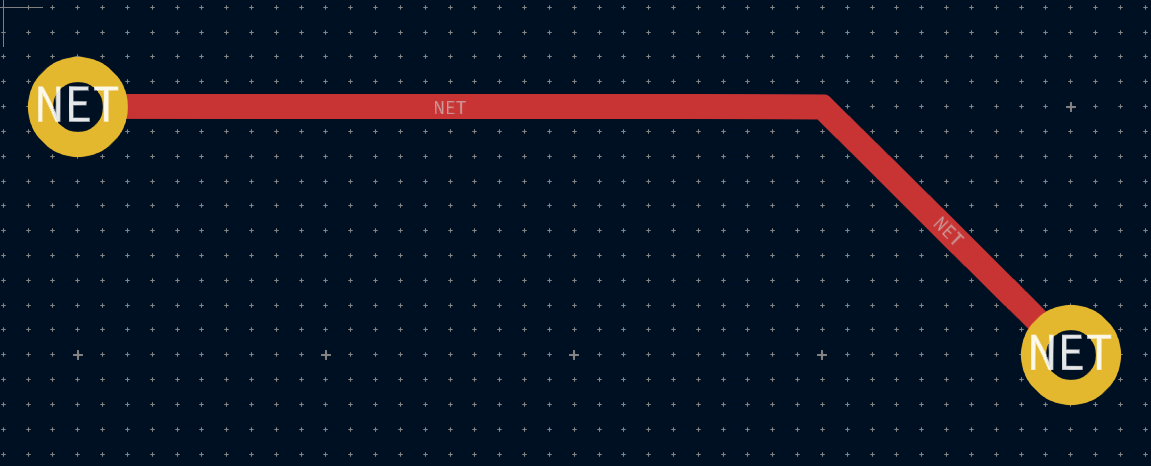
To route tracks, click the Route Tracks ![]() icon (from the drawing toolbar or from the top toolbar under Route) or use the hotkey X. Click on a starting location to select which net to route and begin routing. The net being routed will automatically be highlighted and the allowable clearance for the net will be indicated with a gray outline around the tracks being routed. The clearance outline can be disabled by changing the Clearance Outlines setting in the Display Options section of the Preferences dialog.
icon (from the drawing toolbar or from the top toolbar under Route) or use the hotkey X. Click on a starting location to select which net to route and begin routing. The net being routed will automatically be highlighted and the allowable clearance for the net will be indicated with a gray outline around the tracks being routed. The clearance outline can be disabled by changing the Clearance Outlines setting in the Display Options section of the Preferences dialog.
| The clearance outline shows the maximum clearance from the routed net to any other copper on the PCB. It is possible to use custom design rules to specify different clearances for a net to different objects. These clearances will be respected by the router, but only the largest clearance value will be shown visually. |
When the router is active, new track segments will be drawn from the routing start point to the editor cursor. These tracks are unfixed temporary objects that show what tracks will be created when you use a left-click or the Enter key to fix the route. The unfixed track segments are shown in a brighter color than the fixed track segments. When you exit the router using the Esc key or by selecting another tool, only the fixed track segments will be saved. The Finish Route action (hotkey End) will fix all tracks and exit the router.
While you are routing, you can use the Undo Last Segment command (hotkey Backspace) to unfix the tracks you most recently fixed. You can use this command repeatedly to step back through the route that you have already fixed.
In previous versions of KiCad, using the left mouse button or Enter to fix the routed segments would fix all segments up to but not including the segment ending at the mouse cursor location. In KiCad 6 and later, this behavior is optional, and by default, all segments including the one ending at the mouse cursor location will be fixed. The old behavior can be restored by disabling the "Fix all segments on click" option in the Interactive Router Settings dialog.
While routing, you can hold the Ctrl key to disable grid snapping, and hold the Shift key to disable snapping to objects such as pads and vias.
| Snapping to objects can also be disabled by changing the Magnetic Points preferences in the Editing Options section of the Preferences dialog. We recommend that you leave object snapping enabled in general, so that you do not accidentally end tracks slightly off-center on a pad or via. |
Track posture
When routing in H/V/45 mode, the posture refers to how a set of two track segments connect two points that cannot be reached by a single H/V/45-degree segment. In such a case, the points will be connected by one horizontal or vertical segment and one diagonal (45-degree) segment. The posture refers to the order of these segments: whether the horizontal/vertical segment or the diagonal segment comes first.

KiCad’s router attempts to pick the best posture automatically based on a number of factors. In general, the router will attempt to minimize the number of corners in a route, and will avoid "bad" corners such as acute angles whenever possible. When routing from or to a pad, KiCad will choose the posture that lines up the route with the longest edge of the pad.
In some cases, KiCad cannot guess the posture you intend correctly. To switch the posture of the track while routing, use the Switch Track Posture command (hotkey /).
In situations where there is no obvious "best" posture (for example, when starting a route from a via), KiCad will use the movement of your mouse cursor to select the posture. If you would like the route to begin with a straight (horizontal or vertical) segment, move the mouse away from the starting location in a mostly horizontal or vertical direction. If you would like the route to begin diagonally, move in a diagonal direction. Once the cursor is a sufficient distance away from the routing start location, the posture is "locked" and will no longer change unless the cursor is brought back to the starting location. Detection of posture from the movement of the mouse cursor can be disabled in the Interactive Router Settings dialog as described below.
| If you use the Switch Track Posture command to override the posture chosen by KiCad, the automatic detection of posture from mouse movement will be disabled for the remainder of the current routing operation. |
Track corner mode
KiCad’s router can place tracks with either sharp or rounded (arc) corners when routing in H/V/45 mode. To switch between sharp and rounded corners, use the Track Corner Mode command (hotkey Ctrl+/). When routing with rounded corners, each routing step will place either a straight segment, a single arc, or both a straight segment and an arc. The track posture determines whether the arc or the straight segment will be placed first.
Track corners can also be rounded after routing by using the Fillet Tracks command after selecting the desired tracks.
| Dragging of tracks with arcs is not yet supported. Arcs will be converted back to sharp corners when dragging tracks or when tracks are moved by the router in Shove mode. |
Larghezza pista
The width of the track being routed is determined in one of three ways: if the routing start point is the end of an existing track and the ![]() button on the top toolbar is enabled, the width will be set to the width of the existing track. Otherwise, if the track width dropdown in the top toolbar is set to "use netclass width", the width will be taken from the netclass of the net being routed (or from any custom design rules that specify a different width for the net, such as inside a neckdown area). Finally, if the track width dropdown is set to one of the pre-defined track sizes configured in the Board Setup dialog, this width will be used.
button on the top toolbar is enabled, the width will be set to the width of the existing track. Otherwise, if the track width dropdown in the top toolbar is set to "use netclass width", the width will be taken from the netclass of the net being routed (or from any custom design rules that specify a different width for the net, such as inside a neckdown area). Finally, if the track width dropdown is set to one of the pre-defined track sizes configured in the Board Setup dialog, this width will be used.
| The track width can never be lower than the minimum track width configured in the Constraints section of the Board Setup dialog. If a pre-defined width is added that is lower than this minimum constraint, the minimum constraint value will be used instead. |
KiCad’s router supports a single track width for the active route. In other words, to change widths in the middle of a track, you must end the route and then restart a new route from the end of the previous route. To change the width of the active route, use the hotkeys W and Shift+W to step through the track widths configured in the Board Setup dialog.
Placing vias
While routing tracks, switching layers will insert a through via at the end of the current (unfixed) track. Once you place the via, routing will continue on the new layer. There are several ways to select a new layer and insert a via:
-
By using the hotkey to select a specific layer, such as PgUp to select
F.Cuor PgDn to selectB.Cu. -
By using the "next layer" or "previous layer" hotkeys (+ and -).
-
By using the "Place Via" hotkey (V), which will switch to the next layer in the active layer pair.
-
By using the Select Layer and Place Through Via action (hotkey <), which will open a dialog to select the target layer.
After using any of the above methods to add a via and change layer, but before clicking to fix the via and commit the current trace segment, you can cancel placing the via by pressing V. The via will be removed and routing will continue on the original layer.
You can place a via and end the current trace, without changing layers, by pressing V and then double-clicking or Shift-clicking to place the via.
The size of the via will be taken from the active Via Size setting, accessible from the drop-down in the top toolbar or the Increase Via Size (') and Decrease Via Size (\) hotkeys. Much like track width, when the via size is set to "use netclass sizes", the via sizes configured in the Net Classes section of the Board Setup will be used (unless overridden by a custom design rule).
If microvias or blind/buried vias are enabled in the Constraints section of the Board Setup dialog, these vias can be placed while routing. Use the hotkey Ctrl+V to place a microvia and Alt+Shift+V to place a blind/buried via. Microvias may only be placed such that they connect one of the outer copper layers to an adjacent layer. Blind/buried vias may be placed on any layer.
Vias placed by the router are considered to be part of a routed track. This means that the via net can be updated automatically (just like track nets can), for example when updating the PCB from the schematic changes the net name of the track. In some cases this may not be desired, such as when creating stitching vias. The automatic update of via nets can be disabled for specific vias by turning off the "automatically update via nets" checkbox in the via properties dialog. Vias placed with the Add Free-standing Vias tool are created with this setting disabled.
Routing Convenience Functions
KiCad offers several functions to make certain routing operations more convenient.
If you need to route a number of traces from a set of pads, you can use the Route Selected tool to quickly route from each pad in sequence. Select the pads you want to use as starting points, then press Shift+X to route from each pad in sequence. The router will begin a trace from the first selected pad, which you can route as you would any other trace. When you complete the trace, the router will automatically begin a new trace from the next pad in the selection, in the same order that you selected the pads. Pads that already have traces attached are skipped. You can also skip routing the current trace and move on to the next pad by pressing Esc. You can also select footprints instead of pads; all unrouted pads in the selected footprints will be used as starting points.
If you want to route a number of traces to a set of pads, instead of from the pads, you can use the Route Selected From Other End tool (Shift+E). This tool works the same way as the Route Selected tool, except it uses each selected pad as an end point rather than a starting point. The starting point for each trace is the other end of the ratsnest line for each selected pad.
Routing from the other end is also possible while routing individual traces: press E while routing a trace to commit the current segment and begin routing from the other end of the in-progress trace’s ratsnest line.
Finally, you can quickly unroute traces connected to an object (footprint, pad, or trace) by selecting the object, right-clicking, and selecting Unroute Selected. Any traces connected to the selected object will be removed, starting at the selected object and continuing until another pad is encountered.
Automatically completing traces
KiCad’s router can automatically route individual traces, based on the connections defined in the schematic. This can be thought of as a limited form of auto-routing that considers a single trace at a time. The router will only use the current layer; it will not use vias or change layers.
While routing, press the F key to have the router attempt to automatically finish the current trace. The trace will be automatically routed from the end of the last fixed trace segment to the closest ratsnest anchor. If the router can’t automatically finish the trace, it will allow you to complete the trace manually. This action can also be performed by clicking Attempt Finish in the context menu while routing.
When the router is not the active tool, you can automatically route multiple traces by selecting footprints, pads, and traces to route from and pressing Shift+F. You do not need to select both ends of a desired connection; the router will route from the selected item to its nearest ratsnest anchor. If multiple items were selected, each item will be routed in sequence, in the order that they were selected. If a connection cannot be automatically completed, the tool will pause with the router active so that you can complete the trace manually. With the automatic completion paused for a manual connection, you can press Esc to skip routing the current trace. After manually completing the trace or skipping the connection, the tool will continue attempting to route the remaining connections.
Routing differential pairs
Differential pairs in KiCad are defined as nets with a common base name and a positive and negative suffix. KiCad supports using ` and `-`, or `P` and `N` as the suffix. For example, the nets `USB and USB- form a differential pair, as do the nets USB_P and USB_N. In the first example, the base name is USB, and USB_ in the second. The suffix styles cannot be mixed: the nets USB+ and USB_N do not form a differential pair. Make sure you name your differential pair nets accordingly in the schematic in order to allow use of the differential pair router in the PCB editor.
To route a differential pair, click the Route Differential Pairs ![]() icon (from the drawing toolbar or from the top toolbar under Route) or use the hotkey 6. Click on a pad, via, or the end of an existing differential pair track to start routing. You can start routing from either the positive or negative net of a differential pair.
icon (from the drawing toolbar or from the top toolbar under Route) or use the hotkey 6. Click on a pad, via, or the end of an existing differential pair track to start routing. You can start routing from either the positive or negative net of a differential pair.
| It is not currently possible to start routing a differential pair in the middle of an existing differential pair track. |
The differential pair router will attempt to route the pair of tracks with a gap taken from the design rules (differential pair gap can be configured in the Net Classes section of the Board Setup dialog, or by using custom design rules). If the starting or ending location of the route is a different distance apart from the configured gap, the router will create a short "fan out" section to minimize the length of track where the differential pair is not coupled.
When switching layers or using the Place Via (V) action, the differential pair router will create two vias next to each other. These vias will be placed as close as possible to each other while respecting the design rules for copper and hole-to-hole clearance.
Modifying tracks
After tracks have been routed, they can be modified by moving or dragging, or deleted and re-routed. When a single track segment is selected, the hotkey U can be used to expand the selection to all connected track segments. The first press of U will select track segments between the nearest junctions with pads or vias. The second press of U will expand the selection again to include all track segments connected to the selected track on all layers. Selecting tracks with this technique can be used to quickly delete an entire routed net.
There are two different drag commands that can be used to modify a track segment. The Drag (45-degree mode) command, hotkey D, is used to drag tracks using the router. If the router mode is set to Shove, dragging with this command will shove nearby tracks. If the router mode is set to Walk Around, dragging with this command will walk around or stop at obstacles. The Drag Free Angle command, hotkey G, is used to split a track segment into two and drag the new corner to any location. Drag Free Angle behaves like the Highlight Collisions router mode: obstacles will not be avoided or shoved, only highlighted.
| Dragging of tracks containing arcs is not yet possible. Attempting to drag these tracks will result in the arcs being removed in some cases. It is possible to resize a particular arc by selecting it and using the drag command (D). When resizing an arc using this command, no DRC checking is performed. |
The Move command (hotkey M) can also be used on track segments. This command will pick up the selected track segments, ignoring any attached track segments or vias that are not selected. No DRC checking is done when moving tracks using the Move command.
It is possible to re-route tracks attached to footprints while moving the footprints. To do so, use the drag command (D) with a footprint selected. Any tracks that end at one of the footprint’s pads will be dragged along with the footprint. This feature has some limitations: it only operates in Highlight Collisions mode, so the tracks attached to footprints will not walk around obstacles or shove nearby tracks out of the way. Additionally, only tracks that end at the origin of the footprint’s pads will be dragged. Tracks that simply pass through the pad or that end on the pad at a location other than the origin will not be dragged.
It is possible to modify the width of tracks and the size of vias without re-routing them using the Edit Tracks and Vias dialog. See the section below on bulk editing tools for details.
Length tuning
The length tuning tools can be used to add serpentine tuning shapes to tracks after routing. To tune the length of a track, first pick the appropriate length tuning tool. The single track tuning tool (icon ![]() or hotkey 7) will add serpentine shapes to bring the length of a single track up to the target value. The differential pair tuning tool (icon
or hotkey 7) will add serpentine shapes to bring the length of a single track up to the target value. The differential pair tuning tool (icon ![]() or hotkey 8) will do the same for a differential pair. The differential pair skew tuning tool (icon
or hotkey 8) will do the same for a differential pair. The differential pair skew tuning tool (icon ![]() or hotkey 9) will add length to the shorter member of a differential pair in order to eliminate skew (phase difference) between the positive and negative sides of the pair. As with the Routing icons, the Tuning icons are found in both the Route menu dropdown from the top toolbar and the drawing toolbar on the right.
or hotkey 9) will add length to the shorter member of a differential pair in order to eliminate skew (phase difference) between the positive and negative sides of the pair. As with the Routing icons, the Tuning icons are found in both the Route menu dropdown from the top toolbar and the drawing toolbar on the right.
To select the target length for the length tuning tools, open the Length Tuning Settings dialog from the context menu or with the hotkey Ctrl+L after activating the length tuning tool:
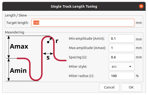
This dialog can also be used to configure the size, shape, and spacing of the meander shapes.
After configuring the target length, click a track in the area that you wish to start placing meander shapes. Move the mouse cursor along the track, and meander shapes will be added. A status window will appear next to the cursor showing the current length of the track and the target length. Click again to finish placing the current meander. Multiple meanders can be placed on the same track if desired.
| The length tuning tools only support tuning the length of point-to-point nets between two pads. Tuning the length of nets with different topologies is not yet supported. |
Interactive router settings
The interactive router settings can be accessed through the Route menu, or by right-clicking on the Route Tracks button in the toolbar. These settings control the router behavior when routing tracks as well as when dragging existing tracks.
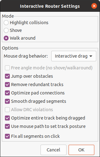
| Setting | Description |
|---|---|
Mode |
Sets the operating mode of the router for creating new tracks and dragging existing tracks. See above for more information. |
Free angle mode |
Allows routing tracks at any angle, instead of just at 45-degree increments. This option is only available if the router mode is set to Highlight collisions. |
Jump over obstacles |
In Shove mode, allows the router to attempt to move colliding tracks behind solid obstacles (such as pads). |
Remove redundant tracks |
Automatically removes loops created in the currently-routed track, keeping only the most recently routed section of the loop. |
Optimize pad connections |
When this setting is enabled, the router attempts to avoid acute angles and other undesirable routing when exiting pads and vias. |
Smooth dragged segments |
When dragging tracks, attempts to combine track segments together to minimize direction changes. |
Allow DRC violations |
In Highlight collisions mode, allows placing tracks and vias that violate DRC rules. It has no effect in other modes. |
Optimize entire track being dragged |
When enabled, dragging a track segment will result in KiCad optimizing the rest of the track that is visible on the screen. The optimization process removes unnecessary corners, avoids acute angles, and generally tries to find the shortest path for the track. When disabled, no optimizations are performed to the track outside of the immediate section being dragged. |
Use mouse path to set track posture |
Attempts to pick the track posture based on the mouse path from the routing start location. |
Fix all segments on click |
When enabled, clicking while routing will fix the position of all the track segments that have been routed, including the segment that ends at the mouse cursor. A new segment will be started from the mouse cursor location. When disabled, the last segment (the one that ends at the mouse cursor) will not be fixed in place and can be adjusted by further mouse movement. |
Forward and back annotation
Update PCB From Schematic (forward annotation)
Use the Update PCB from Schematic tool to sync design information from the Schematic Editor to the Board Editor. The tool can be accessed with Tools → Update PCB from Schematic (F8) in both the schematic and board editors. You can also use the ![]() icon in the top toolbar of the Board Editor. This process is often called forward annotation.
icon in the top toolbar of the Board Editor. This process is often called forward annotation.
| Update PCB from Schematic is the preferred way to transfer design information from the schematic to the PCB. In older versions of KiCad, the equivalent process was to export a netlist from the Schematic Editor and import it into the Board Editor. It is no longer necessary to use a netlist file. |
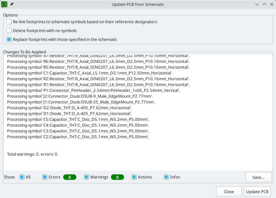
The tool adds the footprint for each symbol to the board and transfers updated schematic information to the board. In particular, the board’s net connections are updated to match the schematic.
The changes that will be made to the PCB are listed in the Changes To Be Applied pane. The PCB is not modified until you click the Update PCB button.
You can show or hide different types of messages using the checkboxes at the bottom of the window. A report of the changes can be saved to a file using the Save… button.
Opzioni
The tool has several options to control its behavior.
| Option | Description |
|---|---|
Re-link footprints to schematic symbols based on their reference designators |
Footprints are normally linked to schematic symbols via a unique identifier created when the symbol is added to the schematic. A symbol’s unique identifier cannot be changed. If checked, each footprint in the PCB will be re-linked to the symbol that has the same reference designator as the footprint. If unchecked, footprints and symbols will be linked by unique identifier as usual, rather than by reference designator. Each footprint’s reference designator will be updated to match the reference designator of its linked symbol. This option should generally be left unchecked. It is useful for specific workflows that rely on changing the links between schematic symbols and footprints, such as refactoring a schematic for easier layout or replicating layout between identical channels of a design. |
Delete footprints with no symbols |
If checked, any footprint in the PCB without a corresponding symbol in the schematic will be deleted from the PCB. Footprints with the "Not in schematic" attribute will be unaffected. If unchecked, footprints without a corresponding symbol will not be deleted. |
Replace footprints with those specified in the schematic |
If checked, footprints in the PCB will be replaced with the footprint that is specified in the corresponding schematic symbol. If unchecked, footprints that are already in the PCB will not be changed, even if the schematic symbol is updated to specify a different footprint. |
Update Schematic from PCB (back annotation)
The typical workflow in KiCad is to make changes in the schematic and then sync the changes to the board using the Update PCB From Schematic tool. However, the reverse process is also possible: design changes can be made in the board and then synced back to the schematic using Tools → Update Schematic From PCB in either the schematic or board editors. This process is often called back annotation.
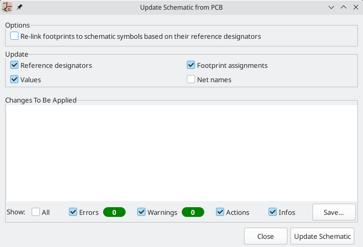
The tool syncs changes in reference designators, values, footprint assignments, and net names from the board to the schematic. Each type of change can be individually enabled or disabled.
The changes that will be made to the schematic are listed in the Changes To Be Applied pane. The schematic is not modified until you click the Update Schematic button.
You can show or hide different types of messages using the checkboxes at the bottom of the window. A report of the changes can be saved to a file using the Save… button.
Opzioni
The tool has several options to control its behavior.
Option |
Description |
Re-link footprints to schematic symbols based on their reference designators |
If checked, each footprint in the PCB will be re-linked to the symbol that has the same reference designator as the footprint. This option is incompatible with updating symbol reference designators. If unchecked, footprints and symbols will be linked by unique identifier as usual, rather than by reference designator. |
Reference designators |
If checked, symbol reference designators will be updated to match the reference designators of the linked footprints. If unchecked, symbol reference designators will not be updated. |
Values |
If checked, symbol values will be updated to match the values of the linked footprints. If unchecked, symbol values will not be updated. |
Footprint assignments |
If checked, footprint assignments will be updated for symbols which have had their footprints changed or replaced in the board. If unchecked, symbol footprint assignments will not be updated. |
Net names |
If checked, the schematic will be updated with any net name changes that have been made in the board. Net labels will be updated or added to the schematic as necessary to match the board. If unchecked, net names will not be updated in the schematic. |
| The Geographical Reannotation feature can be used in combination with backannotating reference designators to reannotate all components in the design based on their location in the layout. |
Back annotation with CMP files
Select changes can also be synced from the PCB back to the schematic by exporting a CMP file from the PCB editor (File → Export → Footprint Association (.cmp) File…) and importing it in the Schematic Editor (File → Import → Footprint Assignments…).
| This method can only sync changes made to footprint assignments and footprint fields. It is recommended to use the Update Schematic from PCB tool instead. |
Geographical re-annotation
| This section of the KiCad documentation has not yet been written. We appreciate your patience as our small team of volunteer documentation writers work to update and expand the documentation. |
Locking
Most objects can be locked through their properties dialogs, by using the right-click context menu, or by using the Toggle Lock hotkey (L). Locked objects cannot be selected unless the "Locked items" checkbox is enabled in the selection filter. Attempting to move locked items will result in a warning dialog:
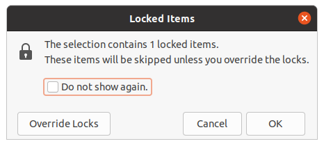
Selecting "Override Locks" in this dialog will allow moving the locked items. Selecting "OK" will allow you to move any unlocked items in the selection; leaving the locked items behind. Selecting "Do not show again" will remember your choice for the rest of your session.
Bulk editing tools
| This section of the KiCad documentation has not yet been written. We appreciate your patience as our small team of volunteer documentation writers work to update and expand the documentation. |
Cleanup tools
| This section of the KiCad documentation has not yet been written. We appreciate your patience as our small team of volunteer documentation writers work to update and expand the documentation. |
Importing graphics
| This section of the KiCad documentation has not yet been written. We appreciate your patience as our small team of volunteer documentation writers work to update and expand the documentation. |
Importing vector drawings from DXF and SVG files
| This section of the KiCad documentation has not yet been written. We appreciate your patience as our small team of volunteer documentation writers work to update and expand the documentation. |
Importing bitmap images
| This section of the KiCad documentation has not yet been written. We appreciate your patience as our small team of volunteer documentation writers work to update and expand the documentation. |