Creazione e modifica di schemi elettrici
Introduzione
Uno schema elettrico progettato con KiCad è più di una semplice rappresentazione grafica di un dispositivo elettronico. Esso normalmente è il punto di ingresso di una catena di sviluppo che permette:
-
Il controllo di validità rispetto ad una serie di regole (Controllo Regole Elettriche (ERC)) per il rilevamento di errori e omissioni.
-
Generazione automatica della DIBA.
-
La generazione di una netlist per software di simulazione tipo SPICE.
-
Definizione di un circuito per il trasferimento delle informazioni nella progettazione del circuito stampato.
Uno schema elettrico consiste principalmente di simboli, fili, etichette, giunzioni, bus e simboli di potenza. Per chiarezza, negli schemi elettrici, è possibile inserire elementi puramente grafici come elementi bus, commenti, e polilinee.
I simboli vengono aggiunti allo schema dalle librerie di simboli. Dopo aver creato lo schema, l’insieme di connessioni e impronte viene importato nell’editor dei circuiti stampati per progettare la scheda.
Gli schemi possono essere contenuti in un unico foglio o suddivisi in più fogli. In KiCad, gli schemi a più fogli sono organizzati gerarchicamente, con un foglio principale e uno o più fogli secondari. Ogni foglio è il proprio file .kicad_sch ed è esso stesso uno schema completo di KiCad. L’utilizzo degli schemi gerarchici è descritto nel capitolo schemi gerarchici.
Operazioni di modifica degli schemi elettrici
Schematic editing tools are located in the right toolbar. When a tool is activated, it stays active until a different tool is selected or the tool is canceled with the Esc key. The selection tool is always activated when any other tool is canceled.
|
Selection tool (the default tool) |
|
Highlight a net by marking its wires and net labels with a different color. If the PCB Editor is also open then copper corresponding to the selected net will be highlighted as well. Net highlighting can be cleared by clicking with the highlight tool in an empty space, or by using the Clear Net Highlighting hotkey (~). |
|
Display the symbol selector dialog to place a new symbol. |
|
Display the power symbol selector dialog to place a new power symbol. |
|
Draw a wire. |
|
Draw a bus. |
|
Draw wire-to-bus entry points. These elements are only graphical and do not create a connection, thus they should not be used to connect wires together. |
|
Place a "no-connection" flag. These flags should be placed on symbol pins which are meant to be left unconnected. "No-connection" flags indicate to the Electrical Rule Checker that the pin is intentionally unconnected and not an error. |
|
Place a junction. This connects two crossing wires or a wire and a pin, which can sometimes be ambiguous without a junction (i.e. if a wire end or a pin is not directly connected to another wire end). |
|
Place a local label. Local labels connect items located in the same sheet. For connections between two different sheets, use global or hierarchical labels. |
|
Place a net class directive label. |
|
Place a global label. All global labels with the same name are connected, even when located on different sheets. |
|
Place a hierarchical label. Hierarchical labels are used to create a connection between a subsheet and the sheet’s parent sheet. See the Hierarchical Schematics section for more information about hierarchical labels, sheets, and pins. |
|
Place a hierarchical subsheet. You must specify the file name for this subsheet. |
|
Import a hierarchical pin from a subsheet. This command can be executed only on hierarchical subsheets. It will create hierarchical pins corresponding to hierarchical labels placed in the target subsheet. |
|
Place a text comment. |
|
Place a text box. |
|
Draw a rectangle. |
|
Draw a circle. |
|
Draw an arc. |
|
Draw lines. Note: Lines are graphical objects and are not the same as wires placed with the Wire tool. They do not connect anything. |
|
Place a bitmap image. |
|
Delete clicked items. |
Griglie
Nell’editor degli schemi il puntatore si sposta sempre sopra una griglia. La griglia può essere personalizzata:
-
La dimensione è modificabile usando il tasto destro del mouse o usando Visualizza → Proprietà griglia….
-
I colori possono essere modificati tramite la scheda Colori presente nella finestra di dialogo delle Preferenze (menu Preferenze → Opzioni generali).
-
La visibilità può essere accesa/spenta usando il pulsante corrispondente nella barra strumenti di sinistra.
La dimensione predefinita della griglia è 50 mils (0.050") o 1,27 millimetri.
Questa è la griglia raccomandata per piazzare simboli e fili in uno schema elettrico, e per piazzare piedini durante la progettazione di un simbolo nell’editor dei simboli.
| Wires connect with other wires or pins only if their ends coincide exactly. Therefore it is very important to keep symbol pins and wires aligned to the grid. It is recommended to always use a 50 mil grid when placing symbols and drawing wires because the KiCad standard symbol library and all libraries that follow its style also use a 50 mil grid. Using a grid size other than 50 mil will result in schematics without proper connectivity! |
È possibile usare anche griglie più piccole, ma queste servono solo per il testo e la grafica dei simboli e non è consigliato per posizionarvi pin e fili.
| Symbols, wires, and other elements that are not aligned to the grid can be snapped back to the grid by selecting them, right clicking, and clicking Align Elements to Grid. |
Magnetismo
Schematic elements such as symbols, wires, text, and graphic lines are snapped to the grid when moving, dragging, and drawing them. Additionally, the wire tool snaps to pins even when grid snapping is disabled. Both grid and pin snapping can be disabled while moving the mouse by using the modifier keys in the table below.
| Su tastiere Apple, usare il tasto Cmd al posto di Ctrl. |
| Modifier Key | Effect |
|---|---|
Ctrl |
Disable grid snapping. |
Shift |
Disable snapping wires to pins. |
Modifica proprietà dell’oggetto
All objects have properties that are editable in a dialog. Use the hotkey E or select Properties from the right-click context menu to edit the properties of selected item(s). You can only open the properties dialog if all the items you have selected are of the same type. To edit the properties of different types of items at one time, see the section below on bulk editing tools.
In properties dialogs, any field that contains a numeric value can also accept a basic math expression that results in a numeric value. For example, a dimension may be entered as 2 * 2mm, resulting in a value of 4mm. Basic arithmetic operators as well as parentheses for defining order of operations are supported.
Lavorare con i simboli
Piazzamento simboli
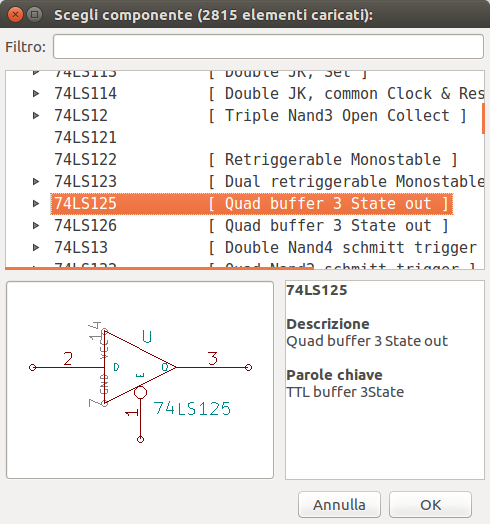
Per piazzare un simbolo nello schema elettrico si può usare il pulsante ![]() o il tasto A. Appare la finestra di dialogo Scegli simboli che consente di scegliere il simbolo da aggiungere. I simboli sono raggruppati per libreria.
o il tasto A. Appare la finestra di dialogo Scegli simboli che consente di scegliere il simbolo da aggiungere. I simboli sono raggruppati per libreria.
By default, only the symbol/library name and description columns are shown. Additional columns can be added by right-clicking the column header and selecting Select Columns.
La finestra di dialogo di scelta del simbolo filtrerà i simboli per nome, parolechiave, descrizione e tutti i campi simbolo aggiuntivi, a seconda di quanto si inserirà nel campo di ricerca.
Alcuni filtri avanzati sono disponibili:
-
Wildcards:
*matches any number of any characters, including none, and?matches any single character. -
Paia di chiavi-valore: se la descrizione di un componente di libreria o parola chiave contiene un marcatore nel formato "chiave:123", si può verificarne la corrispondenza relativa battendo "chiave>123" (maggiore di), "chiave<123" (minore di), ecc. I numeri possono includere uno dei seguenti suffissi indipendenti da maiuscole o minuscole:
p
n
u
m
k
meg
g
t
10-12
10-9
10-6
10-3
103
106
109
1012
ki
mi
gi
ti
210
220
230
240
-
Espressioni regolari: se si ha familiarità con le espressioni regolari, si possono usare anch’esse. Il tipo di espressione regolare usato è di stile espressione regolare avanzato dei wxWidgets, che è simile alle espressioni regolari Perl.
Se il simbolo specifica un’impronta predefinita, questa verrà visualizzata in anteprima in basso a destra. Se il simbolo include filtri impronta, è possibile selezionare impronte alternative che soddisfano i filtri impronta nel menu impronta a discesa a destra.
Dopo aver selezionato un simbolo da posizionare, il simbolo verrà attaccato al cursore. Facendo clic con il pulsante sinistro del mouse sulla posizione desiderata nello schema, il simbolo viene inserito nello schema. Prima di posizionare il simbolo nello schema elettrico, è possibile ruotarlo, renderlo speculare e modificarne i campi, usando i tasti comando o il menu contestuale del tasto destro. Queste azioni possono essere eseguite anche dopo il posizionamento.
Se l’opzione Posiziona copie ripetute è selezionata, dopo aver posizionato un simbolo, KiCad inizierà a posizionare un’altra copia del simbolo. Questo processo continua finché l’utente non preme Esc.
Per i simboli con più unità, se l’opzione Posiziona tutte le unità è selezionata, dopo aver posizionato il simbolo KiCad inizierà a posizionare l’unità successiva nel simbolo. Ciò continuerà fino a quando l’ultima unità sarà stata posizionata o sino a quando l’utente premerà Esc.
Piazzamento simboli di potenza
Un simbolo di potenza è un simbolo che rappresenta una connessione a un collegamento di potenza (N.d.T. come un’alimentazione). I simboli sono raggruppati nella libreria power, quindi possono essere posizionati utilizzando il selettore simboli. Tuttavia, poiché i posizionamenti di simboli potenza sono frequenti, è disponibile lo strumento ![]() . Questo strumento è simile, tranne per il fatto che la ricerca viene eseguita direttamente nella libreria
. Questo strumento è simile, tranne per il fatto che la ricerca viene eseguita direttamente nella libreria power e in qualsiasi altra libreria che contenga simboli di potenza.
Spostamento simboli
I simboli possono essere spostati utilizzando gli strumenti Sposta (M) o Trascina (G). Questi strumenti agiscono sul simbolo selezionato, oppure se nessun simbolo fosse stato selezionato, agiscono sul simbolo sotto il cursore.
Lo strumento Sposta sposta il simbolo stesso senza mantenere connessioni cablate ai piedini del simbolo.
Lo strumento Trascina sposta il simbolo senza interrompere le connessioni cablate ai suoi piedini, e quindi sposta anche i fili collegati.
You can also Drag symbols by clicking and dragging them with the mouse, depending on the Left button drag gesture setting in the Mouse and Touchpad section of Preferences.< Si può anche trascinare i simboli facendo clic e trascinandoli con il mouse, a seconda dell’impostazione Gesture trascinamento del pulsante sinistro nella sezione Mouse e touchpad delle Preferenze.
Symbols can also be rotated (R) or mirrored in the X (X) or Y (Y) directions.
Modifica delle proprietà del simbolo
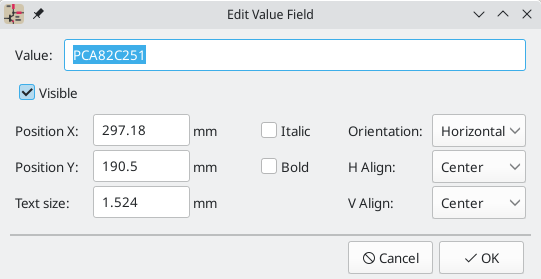
A symbol’s fields can be edited in the symbol’s Properties window. Open the Symbol Properties window for a symbol with the E hotkey or by double-clicking on the symbol.
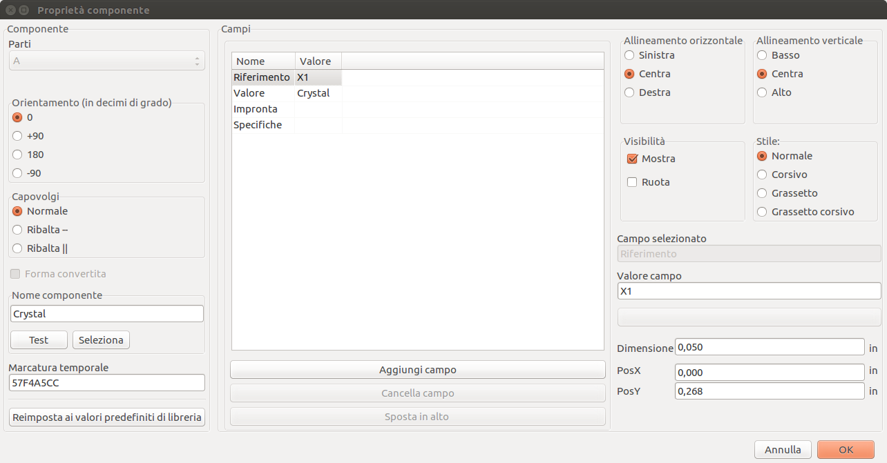
The Symbol Properties window displays all the fields of a symbol in a table. New fields can be added, and existing fields can be deleted, edited, reordered, moved, or resized.
Il nome e il valore di ciascun campo possono essere visibili o nascosti e sono disponibili diverse opzioni di formattazione: allineamento orizzontale e verticale, orientamento, posizione, carattere, colore del testo, dimensione del testo ed enfasi in grassetto/corsivo. Il posizionamento automatico del campo può anche essere abilitato in base al campo. La posizione visualizzata è sempre indicata per un simbolo visualizzato normalmente (nessuna rotazione o specularità) ed è relativa al punto di ancoraggio del simbolo.
| Le opzioni di formattazione per i campi del simbolo possono essere visualizzate o nascoste facendo clic con il pulsante destro del mouse sulla riga dell’intestazione della tabella campi simbolo abilitanto o disabilitando le colonne desiderate. Non tutte le colonne sono visibili per impostazione predefinita. |
The Update Symbol from Library… button is used to update the schematic’s copy of the symbol to match the copy in the library. The Change Symbol… button is used to swap the current symbol to a different symbol in the library. These functions are described later.
Edit Symbol… opens the Symbol Editor to edit the copy of the symbol in the schematic. Note that the original symbol in the library will not be modified. The Edit Library Symbol… button opens the Symbol Editor to edit the original symbol in the library. In this case, the symbol in the schematic will not be modified until the user clicks the Update Symbol from Library… button.
Symbols have several attributes that affect how the symbols are treated by other parts of KiCad.
Exclude from simulation prevents the symbol from being included in SPICE simulations.
Exclude from bill of materials prevents the component from being included in BOM exports.
Exclude from board means that the symbol is schematic-only, and a corresponding footprint will not be added to the PCB.
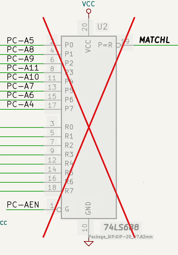
Do not populate means that the component should not be attached to the PCB, although a corresponding footprint should still be added to the board. DNP symbols appear desaturated and with a red "X" over them in the schematic, as shown below.
Modifica individuale dei campi del simbolo
An individual symbol text field can be edited directly with the E hotkey (with a field selected instead of a symbol) or by double-clicking on the field.
Some symbol fields have their own hotkey to edit them directly. With the symbol selected, the Reference, Value, and Footprint fields can be edited with the U, V, or F hotkeys, respectively.
The options in this dialog are the same as those in the full Symbol Properties dialog, but are specific to a single field.
Symbol fields can be automatically moved to an appropriate location with the Autoplace Fields action (select a symbol and press O). Field autoplacement is configurable in the Schematic Editor’s Editing Options, including a setting to always autoplace fields.
Updating and exchanging symbols
When a symbol is added to the schematic, KiCad embeds a copy of the library symbol in the schematic so that the schematic is independent of the system libraries. Symbols that have been added to the schematic are not automatically updated when the library changes. Library symbol changes are manually synced to the schematic so that the schematic does not change unexpectedly.
To update symbols in the schematic to match the corresponding symbol, use Tools → Update Symbols from Library, or right click a symbol and select Update Symbol from Library. You can also access the tool from the symbol properties dialog.
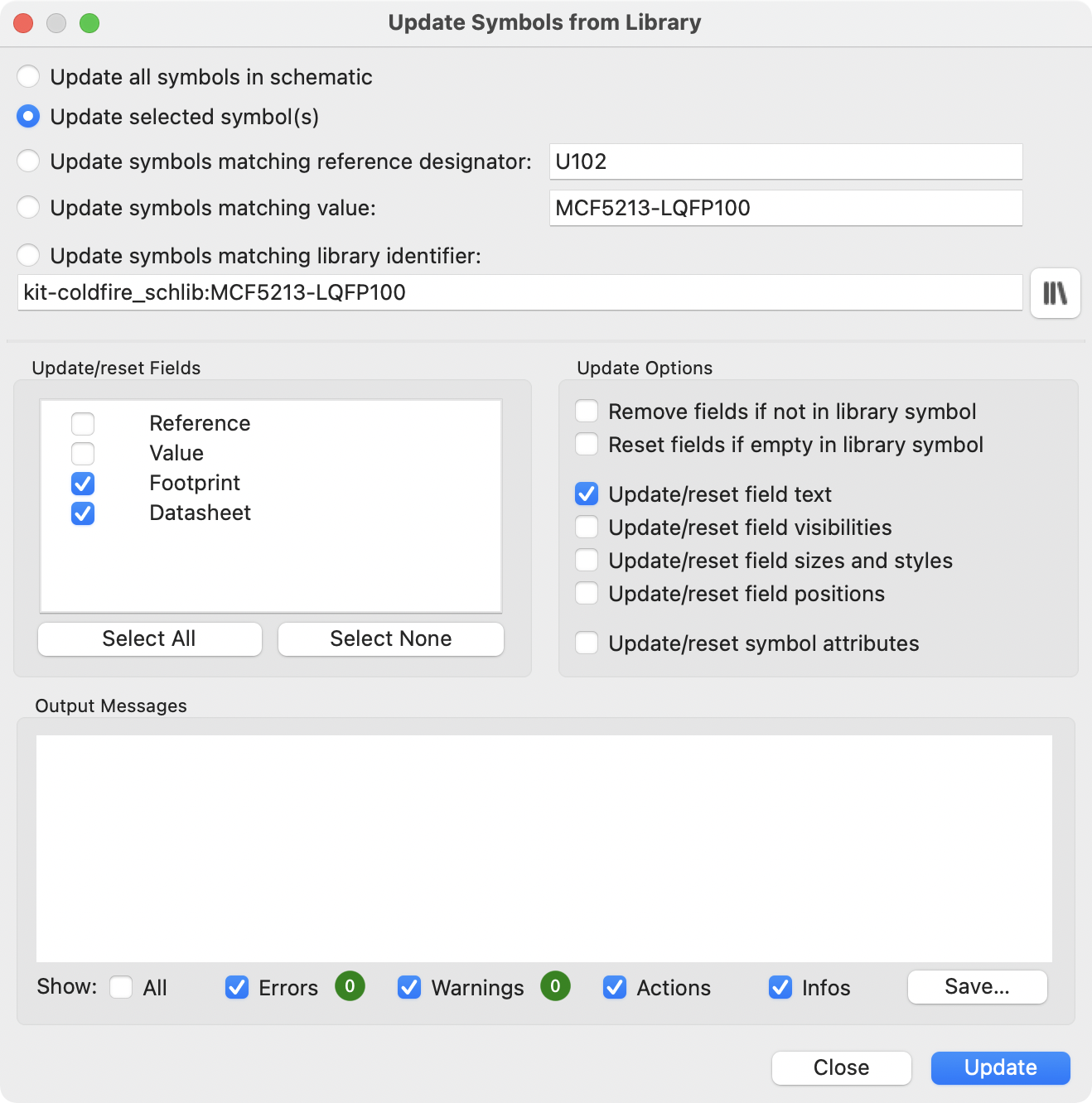
The top of the dialog has options to choose which symbols will be updated. You can update all symbols in the dialog, update only the selected symbols, or update only the symbols that match a specific reference designator, value, or library identifier. The reference designator and value fields support wildcards: * matches any number of any characters, including none, and ? matches any single character.
The middle of the dialog has options to control what parts of the symbol will be updated. You can select specific fields to update or not update, which properties of the fields to update (text, visibility, size and style, and position), and how to handle fields that are missing or empty in the library symbol. You can also choose whether to update symbol attributes, such as do not populate and exclude from simulation / bill of materials / board.
The bottom of the dialog displays messages describing the update actions that have been performed.
To change an existing symbol to a different symbol, use Edit → Change Symbols…, or right click an existing symbol and select Change Symbol…. This dialog is also accessible from the symbol properties dialog.
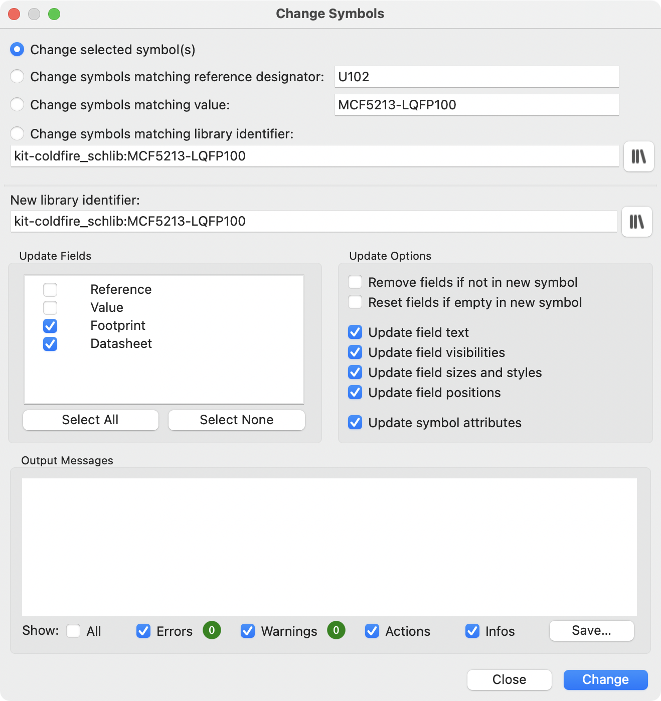
The options for the Change Symbols dialog are very similar to the Update Symbols from Library dialog.
Another way to swap existing symbols for new ones is to use Tools → Edit Symbol Library Links…. This dialog contains a table of every symbol in the design, grouped by current library symbol. By choosing a new symbol in the New Library Reference column, you can make all instances of the existing symbol instead point to the new symbol. If the Update symbol fields from new library option is used, the contents of the existing symbols' fields will be updated to match the new symbols' fields.
The Map Orphans button attempts to automatically remap orphaned symbols to symbols with the same name in an active library. For example, if there is a symbol with the current library reference mylib:symbol123, but the mylib library cannot be found, the Map Orphans button will attempt to find a symbol named symbol123 in any of the libraries that are present. This button is only enabled if orphaned symbols are present in the schematic (see the legacy schematics section).
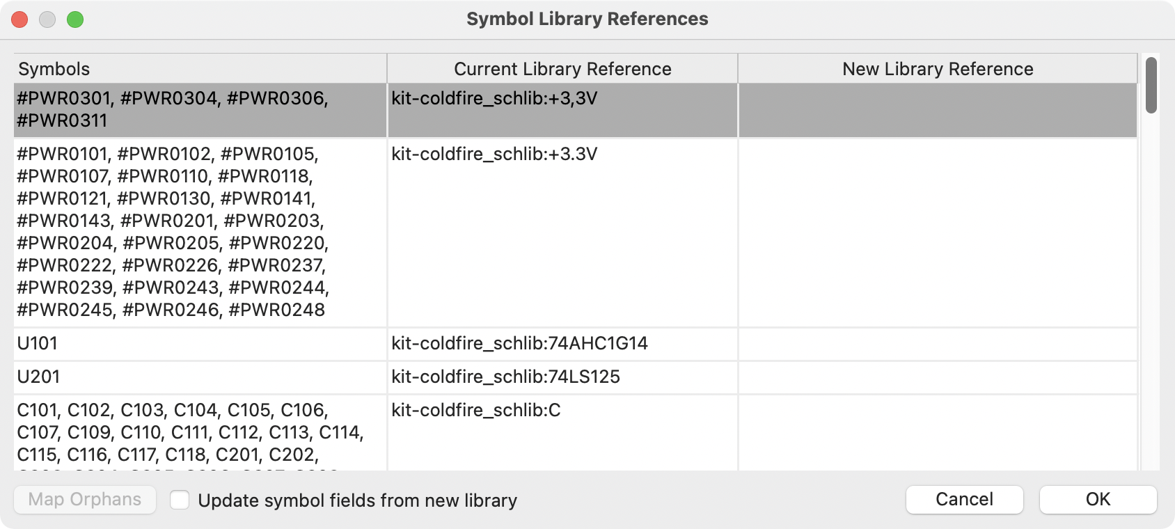
This dialog is primarily useful for managing symbols that appear in multiple libraries, when you want to switch from one library to another. For example, if a schematic uses symbols that are in both a global library and a project-specific library, the Symbol Library References dialog could be used to switch between using the global symbols or the equivalent project-specific symbols. It does not have features for fine-grained control of how fields are updated; for that, use the Change Symbols dialog.
Tabella campi del simbolo
The Symbol Fields Table allows you to view and modify field values for all symbols in a spreadsheet interface. You can open the Symbol Fields Table with the ![]() button.
button.
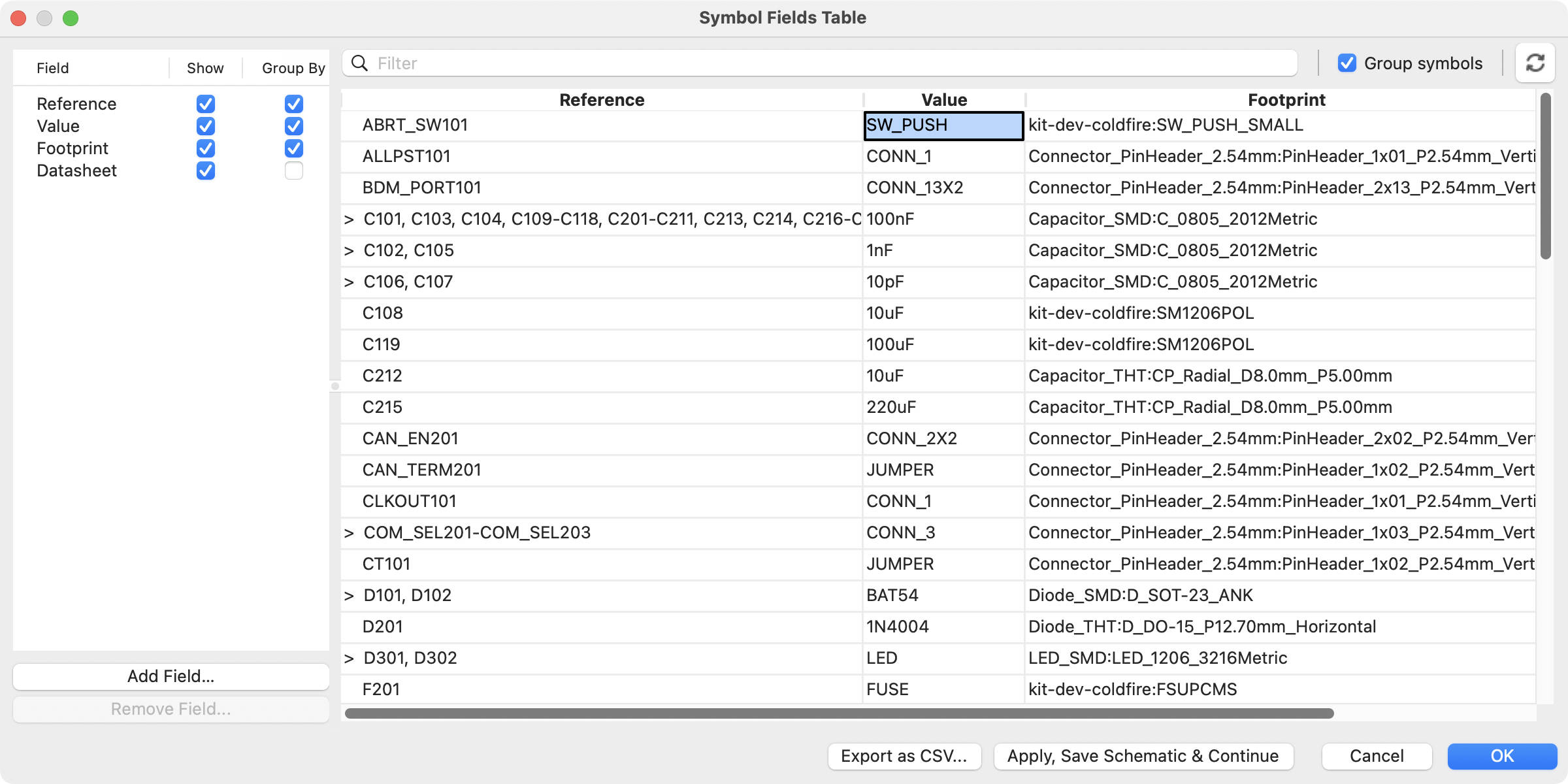
Cells are navigated with the arrow keys, or with Tab / Shift+Tab to move right / left and Enter / Shift+Enter to move down / up, respectively.
A range of cells can be selected by clicking and dragging. The whole range of selected cells will be copied (Ctrl+C) or pasted into (Ctrl+V) on a copy or paste action. Copying a range of cells from the table can be useful for creating a BOM. More details of copying and pasting cells are described below.
Any symbol field can be shown or hidden using the Show checkboxes on the left, or by right-clicking on the header of the table. New symbol fields can be added using the Add Field… button.
Similar symbols can optionally be grouped by any symbol field using the Group By checkboxes. Grouped symbols are shown in a single row in the table. The grouped row can be expanded to show the individual symbols by clicking the arrow at the left of the row. The Group Symbols checkbox enables or disables symbol grouping, and the ![]() button recalculates groupings.
button recalculates groupings.
Symbols can be filtered using the Filter textbox at the top. The filter supports wildcards: * matches any number of any characters, including none, and ? matches any single character.
You can use the Export as CSV… button to save the symbol fields to an external file. This can be used as a simple BOM generation tool, although the BOM tool provides better control over the generated output.
Trucchi per semplificare lo riempimento dei campi
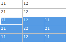
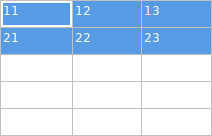
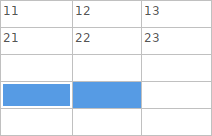
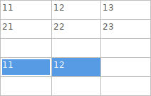
Esistono diversi metodi speciali di copia/incolla nel foglio di calcolo per incollare i valori in regioni più grandi, comprese le celle incollate con incremento automatico. Queste funzionalità possono essere utili quando si incollano valori condivisi in più simboli.
Questi metodi sono illustrati sotto.
| 1. Copia (Ctrl+C) | 2. Selezione celle obiettivo | 3. Incolla (Ctrl+V) |
|---|---|---|
|
|
|
|
|
|
|
|
|
|
|
|
|
|
|
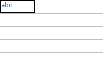
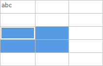
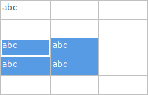
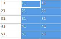
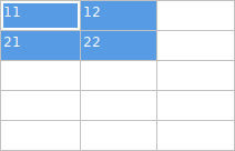
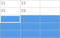
| Queste tecniche sono disponibili anche in altre finestre di dialogo con elementi di controllo a griglia. |
Reference Designators and Symbol Annotation
Reference designators are unique identifiers for components in a design. They are often printed on a PCB and in assembly diagrams, and allow you to match symbols in a schematic to the corresponding components on a board.
In KiCad, reference designators consist of a letter indicating the type of component (R for resistor, C for capacitor, U for IC, etc.) followed by a number. If the symbol has multiple units then the reference designator will also have a trailing letter indicating the unit. Symbols that don’t have a reference designator set have a ? character instead of the number. Reference designators must be unique.
Reference designators can be automatically set when symbols are added to the schematic, and you can set or reset reference designators yourself by manually editing an individual symbol’s reference designator field or in bulk using the Annotation tool.
| The process of setting a symbol’s reference designator is called annotation. |
Auto annotazione
When auto-annotation is enabled, symbols will be automatically annotated when they are added to the schematic. You can enable auto-annotation by checking the Automatically annotate symbols checkbox in the Schematic Editor → Annotation Options pane in Preferences. Auto-annotation can also be toggled using the ![]() button in the left toolbar.
button in the left toolbar.
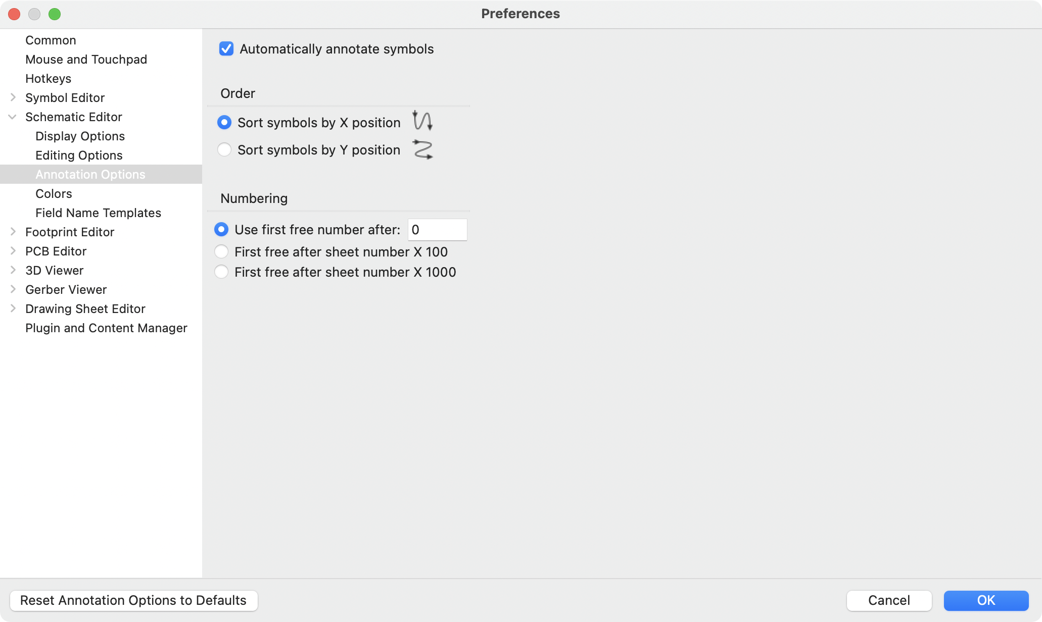
When multiple symbols are added simultaneously, they are annotated according to the Order setting, sorted by either X or Y position.
The Numbering option sets the starting number for new reference designators. This can be the lowest available number, or a number based on the sheet number.
For more information about annotation options, see the documentation for the Annotation tool.
Strumento di annotazione
Lo strumento di annotazione assegna automaticamente i riferimenti a simboli nello schema. Per eseguire lo strumento di annotazione fare clic sull’icona ![]() nella barra strumenti in alto.
nella barra strumenti in alto.
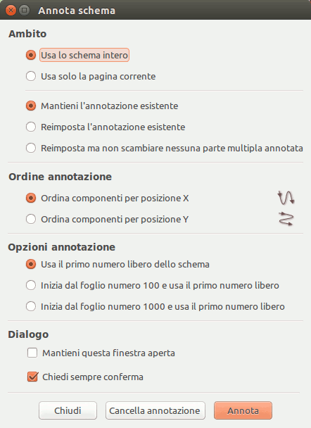
The tool provides several options to control how symbols are annotated.
Scope: Selects whether annotation is applied to the entire schematic, to only the current sheet, or to only the selected symbols. If the Recurse into subsheets option is selected, symbols in subsheets of the selected scope will be reannotated; otherwise symbols in subsheets will not be reannotated. For example, if Recurse into subsheets and Selection only selected, symbols in any selected subsheets will be reannotated.
Options: Selects whether annotation should apply to all symbols and reset *existing reference designators, or apply only to unannotated symbols.
Order: Chooses the direction of numbering. If symbols are sorted by X position, all symbols on the left side of a schematic sheet will be lower numbered than symbols on the right side of the sheet. If symbols are sorted by Y position, all symbols on the top of a sheet will be lower numbered than symbols at the bottom of the sheet.
Numbering: Selects the starting point for numbering reference designators. The lowest unused number above the starting point is picked for each reference designator. The starting point can be an arbitrary number (typically zero), or it can be the sheet number multiplied by 100 or 1000 so that each part’s reference designator corresponds to the schematic page it is on.
The Clear Annotation button clears all reference designators in the selected scope.
Annotation messages can be filtered with the checkboxes at the bottom or saved to a report using the Save… button.
Connessioni elettriche
There are two primary ways to establish connections: wires and labels. Wires make direct connections, while labels connect to other labels with the same name. Both wires and labels are shown in the schematic below.
Connections can also be made with buses and with implicit connections via hidden power pins.
This section will also discuss two special types of symbols that can be added with the "Power symbol" button on the right toolbar:
-
Simboli di potenza: simboli per connettere una linea di potenza o di massa.
-
PWR_FLAG: a specific symbol for indicating that a net is powered when it is not connected to a power output pin (for example, a power net that is supplied by an off-board connector).
Fili
I fili vengono utilizzati per stabilire direttamente collegamenti elettrici tra due punti. Per stabilire una connessione, un segmento di filo deve essere collegato per la sua estremità a un altro segmento o ad un pin. Solo le estremità dei fili creano connessioni; se un filo attraversa il centro di un altro filo, non verrà effettuata una connessione.
Unconnected wire ends have a small square that indicates the connection point. The square disappears when a connection is made to the wire end. Unconnected pins have a circle, which also disappears when a connection is made.
| Wires connect with other wires or pins only if their ends coincide exactly. Therefore it is important to keep symbol pins and wires aligned to the grid. It is recommended to always use a 50 mil grid when placing symbols and drawing wires because the KiCad standard symbol library and all libraries that follow its style also use a 50 mil grid. |
| Symbols, wires, and other elements that are not aligned to the grid can be snapped back to the grid by selecting them, right clicking, and selecting Align Elements to Grid. |
Disegno e modifica fili
To begin connecting elements with wire, use the Wire tool ![]() in the right toolbar (w). Wires can also be automatically started by clicking on an unconnected symbol pin or wire end.
in the right toolbar (w). Wires can also be automatically started by clicking on an unconnected symbol pin or wire end.
You can restrict wires to 90 degree angles using the ![]() button in the left toolbar, or to 45 degree angles with the
button in the left toolbar, or to 45 degree angles with the ![]() button. The
button. The ![]() button allows you to place wires at any angle. You can cycle through these modes using Shift+Space, or select the desired mode in Preferences → Schematic Editor → Editing Options. These modes affect graphic lines in addition to wires.
button allows you to place wires at any angle. You can cycle through these modes using Shift+Space, or select the desired mode in Preferences → Schematic Editor → Editing Options. These modes affect graphic lines in addition to wires.
As in the PCB editor, the / hotkey switches wire posture.
Wires can be moved and edited using the Move (M) or Drag (G) tools. As with symbols, the Move tool moves only the selected segment, without maintaining existing connections to other segments. The Drag tool maintains existing connections.
You can select connected wires using the Select Connection tool (Alt+4). This tool selects all connected wire segments until it reaches a junction, starting with the selected segment or the segment under the cursor. Using the tool again expands the existing selection to the next junction.
You can break a wire segment into two pieces by right-clicking a wire and selecting Slice. The segment will be separated at the current mouse position. You can also separate a wire segment from the adjacent segments by right-clicking the segment and selecting Break.
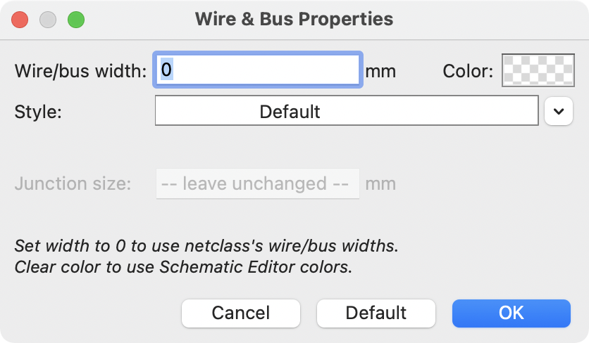
Normally the line style of a wire follows the net’s netclass settings (nets are in the Default netclass if no other netclass is specified). However, the line style for the selected wire segments can be overridden in the wire’s properties dialog (E when a wire segment is selected). The wire’s width, color, and line style (solid, dashed, dotted, etc.) can be set. Setting the width to 0, clearing the color, and using the Default line style uses the default width, color, and style, respectively, from the netclass settings. If a wire junction is included in the selection, the junction size can also be edited here.
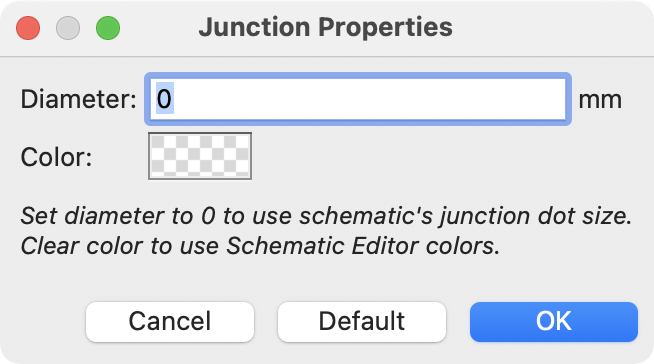
Giunzioni di fili
I fili che si incrociano non sono implicitamente connessi. È necessario collegarli assieme esplicitamente con un punto di giunzione se si vuole stabilire una connessione (pulsante ![]() nella barra strumenti a destra). I punti di giunzione verranno aggiunti automaticamente ai fili che cominciano o finiscono su altri fili esistenti.
nella barra strumenti a destra). I punti di giunzione verranno aggiunti automaticamente ai fili che cominciano o finiscono su altri fili esistenti.
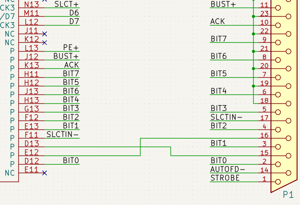
I punti di giunzione sono utilizzati nella figura dello schema precedente sui fili collegati ai pin 18, 19, 20, 21, 22 e 23 di P1.
Junction size automatically follows the schematic’s Junction dot size setting in Schematic Setup → General → Formatting. Color follows the netclass setting. The automatic size and color can be overridden in each junction dot’s properties; a size of 0 is equivalent to the schematic default size, and clearing the color uses the netclass color.
Etichette
Labels are used to assign net names to wires and pins. Wires with the same net name are considered to be connected, so labels can be used to make connections without drawing direct wire connections.
Una net può avere un solo nome. Se due etichette diverse vengono posizionate sulla stessa rete, verrà generata una violazione ERC. Nella netlist verrà utilizzato solo uno dei nomi di net. Il nome della net finale è determinato in base alle regole descritte di seguito.
There are three types of labels, each with a different connection scope.
-
Local labels, also referred to simply as labels, only make connections within a sheet. Add a local label with the
 button in the right
toolbar.
button in the right
toolbar. -
Global labels make connections anywhere in a schematic, regardless of sheet. Add a global label with the
 button in the right
toolbar.
button in the right
toolbar. -
Hierarchical labels connect to hierarchical sheet pins and are used in hierarchical schematics for connecting child sheets to their parent sheet. Add a hierarchical label with the
 button in the right toolbar.
| Labels that have the same name will connect, regardless of the label type, if they are in the same sheet. |
Aggiunta e modifica etichette
After using the appropriate button or hotkey to create a label, the Label Properties dialog appears.
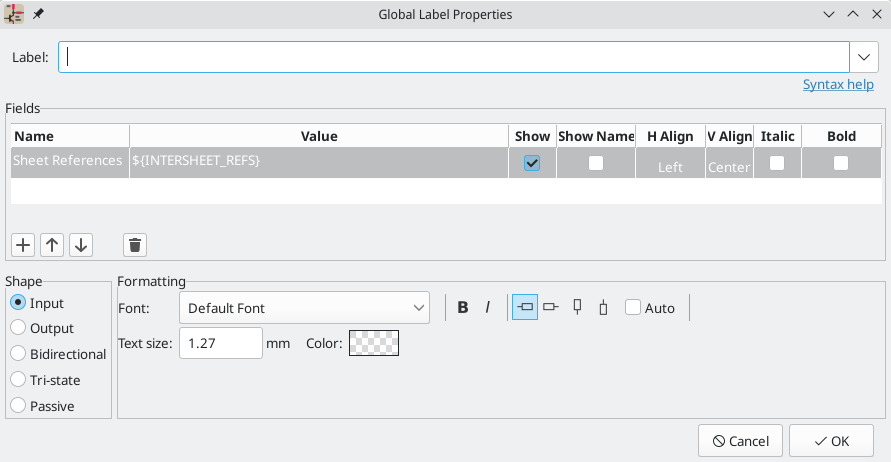
The Label field sets the label’s text, which determines the net that the label assigns to its attached wire. Label text supports markup for overbars, subscripts, etc., as well as variable substitution. Use the Syntax help link in the dialog for a summary.
There are several options to control the label’s appearance. You can change the font, size, and color of the text, and set bold and italic emphasis. You can also set the orientation of the text relative to the label’s connection point. Hierarchical and global labels have several additional options: the Auto option automatically sets the label orientation based on the connected schematic elements, and Shape option controls the shape of the label outline (Input, Output, Bidirectional, Tri-state, or Passive). The outline shape is purely visual and has no electrical consequence.
| The default text size can be set for a schematic in Schematic Setup, and the default font can be set in Preferences. |
| Global labels have additional settings to control margins around the label text in the Schematic Setup dialog. |
Labels can also have fields added to them. Two fields have special meaning (Net Class and Sheet References, described below), but arbitrary fields can also be added. Label fields behave like symbol fields: you can show or hide their name and value and adjust the alignment, orientation, position, size, font, color, and emphasis.
| Le opzioni di formattazione per i campi etichetta possono essere visualizzate o nascoste facendo clic con il pulsante destro del mouse sulla riga dell’intestazione della tabella campi etichetta e abilitando o disabilitando le colonne desiderate. Non tutte le colonne sono visibili per impostazione predefinita. |
Like symbol fields, label fields can be edited individually by opening the properties of a specific label field from the schematic (double click the label field, or use E).
After accepting the label properties, the label is attached to the cursor for placement. The connection point for a label is the small square in the corner of the label. The square disappears when the label is connected to a wire or the end of a pin.

The connection point’s position relative to the label text can be changed by choosing a different label orientation in the label’s properties, or by mirroring/rotating the label.
The Label Properties dialog can be accessed at any time by selecting a label and using the E hotkey, double-clicking on the label, or with Properties… in the right-click context menu.
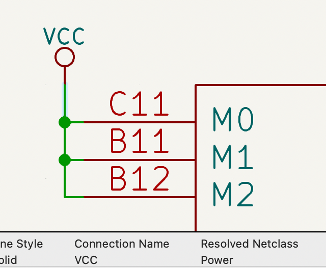
Assigning net classes with labels
In addition to assigning net names, labels can be used to assign net classes. A label field named Net Class assigns the specified netclass to the net associated with the label. To make it easier to assign net classes in this way, Net Class is the default name for new label fields, and Net Class fields present a dropdown list of all the net classes in the design. Net classes must be created in the Schematic Setup or Board Setup windows before they can be assigned with a label field.
For more information about assigning netclasses, see the netclass documentation.
Inter-sheet references
Global labels can display inter-sheet references, which are a list of page numbers for other places in the schematic where the same global label appears. Clicking an inter-sheet reference travels to the listed page. If multiple references are listed, clicking the reference list brings up a menu to select the desired page.
Inter-sheet references are globally controlled in the Schematic Setup window’s Formatting page. References can be enabled or disabled, and the displayed format for the list can be adjusted, including with optional prefix or suffix characters.
The image below shows a global label with inter-sheet references to two other schematic pages. A prefix and suffix of [ and ], respectively, were added in Schematic Setup.
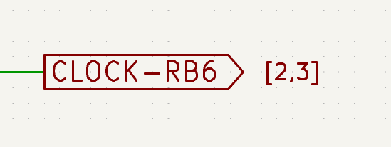
A Sheet References field with value ${INTERSHEET_REFS} is automatically added to global labels, and is used to control the appearance of inter-sheet references for that label. The ${INTERSHEET_REFS} text variable gets expanded to the full list of inter-sheet references for the global label, as configured in Schematic Setup. Visibility of inter-sheet references is globally controlled in Schematic Setup rather than with the Sheet References field visibility control. The Sheet References field has no meaning for other types of labels.
Buses
I bus sono un modo per raggruppare segnali in relazione tra loro in uno schema elettrico, in modo da semplificare i progetti complessi. I bus possono essere disegnati come i fili usando lo strumento bus ![]() , e i loro nomi vengono assegnati usando le etichette allo stesso modo di come si fa con i fili dei segnali.
, e i loro nomi vengono assegnati usando le etichette allo stesso modo di come si fa con i fili dei segnali.
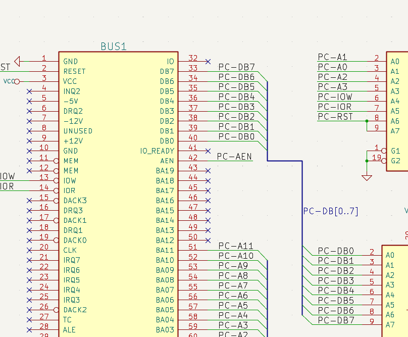
Nello schema elettrico seguente, molti piedini sono connessi a dei bus, cioè le linee spesse blu al centro.
Membri di bus
There are two types of bus in KiCad 6.0 and later: vector buses and group buses.
Un bus vettoriale è un insieme di segnali che cominciano con un prefisso comune e finiscono con un numero. I bus vettoriali hanno nome nella forma <PREFISSO>[M..N] dove PREFISSO è un qualsiasi nome di segnale valido, M è il primo numero del suffisso, e N è l’ultimo numero del suffisso. Per esempio, il bus DATA[0..7] contiene i segnali DATA0, DATA1, e così via fino a DATA7. Non importa in quale ordine M ed N vengono specificati, ma entrambi devono essere positivi.
Un bus di gruppo è un insieme di uno o più segnali e/o bus vettoriali. I bus di gruppo possono essere usati per tenere assieme segnali correlati anche quando questi hanno nomi diversi. I bus di gruppo usano una sintassi etichetta speciale:
<NOME_OPZIONALE>{SEGNALE1 SEGNALE2 SEGNALE3}
I membri del gruppo sono elencati dentro parentesi graffe ({}) separati da spazi. Il nome opzionale del gruppo va prima della prima parentesi. Se il bus di gruppo è anonimo, i collegamenti risultanti sul C.S. saranno semplicemente i nomi dei segnali dentro il gruppo. Se il bus di gruppo possiede un nome, i collegamenti risultanti avranno il nome come prefisso, con un punto (.) di separazione tra il prefisso e il nome del segnale.
Per esempio, il bus {SCL SDA} ha due segnali membri, e nella netlist questi segnali saranno SCL e SDA. Il bus USB1{DP DM} genererà collegamenti chiamati USB1.DP e USB1.DM. Per progetti con bus grandi, ripetuti tra diversi circuiti simili, l’uso di questa tecnica può far risparmiare tempo.
I bus di gruppo possono contenere anche bus vettoriali. Per esempio, il bus MEMORY{A[7..0] D[7..0] OE WE} contiene sia bus vettoriali che segnali normali, il ché porterà a del collegamenti del tipo MEMORY.A7 e MEMORY.OE sul C. S. .
I fili di bus si possono disegnare e collegare allo stesso modo dei fili dei segnali, compreso l’uso di giunzioni per creare connessioni tra fili che si incrociano. Come per i segnali, i bus non possono avere più di un nome — se due etichette in conflitto sono associate allo stesso bus, verrà generato un errore di controllo regole elettriche (ERC).
Connessioni tra membri di bus
Piedini connessi tra gli stessi membri di un bus devono essere connessi da etichette. Non è possibile connettere un piedino direttamente ad un bus; questo tipo di connessione sarà ignorata da KiCad.
Nell’esempio sopra, le connessioni vengono effettuate dalle etichette piazzate sui fili connessi ai piedini. Le voci di bus (segmenti di filo a 45 gradi) sono solo elementi grafici, e non sono necessarie per formare connessioni logiche.
In effetti, usando il comando di ripetizione (Ins), le connessioni possono essere eseguite molto velocemente nel modo seguente, se i piedini del componente sono allineati in ordine incrementale (una pratica comune in componenti come memorie, microprocessori, ecc.):
-
Piazzare la prima etichetta (per esempio
PCA0) -
Usare il tasto di ripetizione quanto serve per piazzare membri. KiCad creerà automaticamente le etichette successive (
PCA1,PCA2…) allineate verticalmente, teoricamente nella esatta posizione degli altri piedini. -
Disegnare il filo sotto la prima etichetta. Usare poi il comando di ripetizione per piazzare gli altri fili sotto le etichette.
-
Se necessario, piazzare le voci di bus allo stesso modo (piazzare la prima voce, poi usare il tasto di ripetizione).
|
Nella sezione Editor schemi elettrici → Opzioni di modifica del menu delle preferenze, è possibile impostare i parametri di ripetizione:
|
Dispiegamento bus
Lo strumento di dispiegamento permette di estrarre velocemente i segnali da un bus. Per dispiegare un segnale, fare clic con il tasto destro del mouse su un oggetto di tipo bus (un filo di bus, ecc) e scegliere Dispiega bus. In alternativa, usare il tasto comando Dispiega bus (predeinito:C) quando il puntatore è posizionato sopra un oggetto di tipo bus. Il menu permette di selezionare quale membro del bus dispiegare.
Dopo aver selezionato il membro del bus, il successivo clic posizionerà l’etichetta del membro del bus alla posizione desiderata. Lo strumento genera automaticamente una voce bus ed un filo in direzione della posizione dell’etichetta. Dopo il posizionamento dell’etichetta, si può continuare a posizionare altri segmenti di filo (per esempio, per connetterli ai pin di un componente) e completare il collegamento in uno qualsiasi dei normali metodi.
Alias di bus
Gli alias di bus sono scorciatoie che permettono di lavorare con grandi insiemi di bus in modo più efficiente. Essi permettono di definire un gruppo di bus e dare ad esso un nome corto che può essere usato poi al posto del nome completo in tutto lo schema elettrico.
To create bus aliases, open the Bus Alias Definitions pane in Schematic Setup.
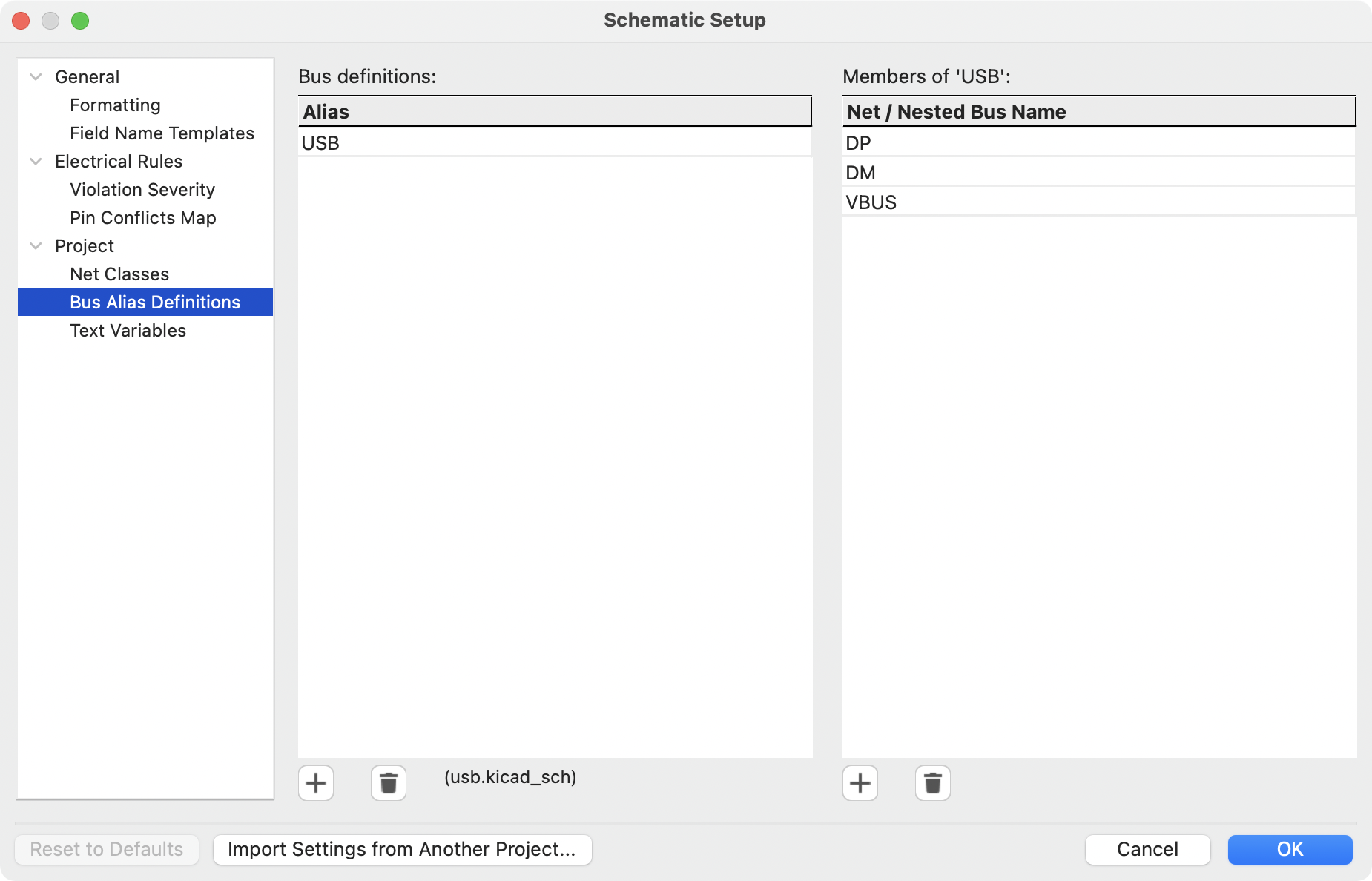
Ad un alias si può dare come nome un qualsiasi nome di segnale valido. Usando la finestra di dialogo, si possono aggiungere segnali o bus vettoriali all’alias. Come scorciatoia, si può battere o incollare dentro un’elenco di segnali e/o buse separati da spazi, e questi verranno aggiunti alla definizione di alias. In questo esempio, definiamo un alias chiamato USB con membri DP, DM, e VBUS.
Dopo la definizione di un alias, esso può essere usato in una etichetta di bus di gruppo mettendo il nome dell’alias dentro le parentesi graffe del bus di gruppo: {USB}. Ciò ha lo stesso effetto dell’etichettare il bus {DP DM VBUS}. Si può anche aggiungere un nome prefisso al gruppo, come USB1{USB}, il che da come risultati collegamenti come USB1.DP come descritto sopra. Per bus complessi, l’uso di alias può rendere l’etichettatura dello schema elettrico molto più corta. Si faccia attenzione al fatto che gli alias sono solo scorciatoie, e che il nome dell’alias non viene incluso nella netlist.
Bus aliases are saved in the schematic file that is opened when the alias is created. The Bus Alias Definitions window shows the schematic file associated with the selected alias at the bottom of the alias list. Any aliases created in a given schematic sheet are available to use in any other schematic sheet that is in the same hierarchical design. If multiple sheets in a hierarchical design contain identically-named bus aliases, the aliases must all have the same members. ERC will report a violation if multiple bus aliases with the same name do not have consistent members.
Bus con più di una etichetta
KiCad 5.0 e versioni precedenti permettevano la connessione di bus con diverse etichette assieme, e collegavano assieme i membri di detti bus durante la creazione della netlist. Questo comportamento è stato eliminato in KiCad 6.0 perché è incompatibile con i bus di gruppo, e anche perché tendeva a creare confusione nelle netlist perché il nome che un dato segnale avrebbe ricevuto non era facilmente predicibile.
Se si apre un progetto che faceva uso di questa caratteristica in una versione moderna di KiCad, si potrà osservare la finestra di dialogo di ``Migrazione bus'' che vi guiderà attraverso la procedura di aggiornamento dello schema in modo tale da garantire l’esistenza di una sola etichetta per un dato insieme di collegamenti bus.
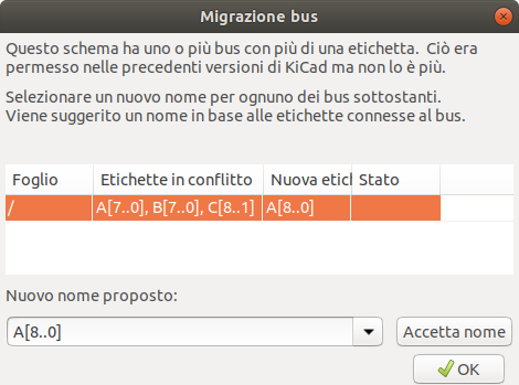
Per ogni insieme di fili di bus che ha più di una etichetta, è necessario scegliere l’etichetta da tenere. Il menu a discesa permette di scegliere tra le etichette che esistono nel progetto, oppure è anche possibile scegliere un nome ancora diverso inserendolo manualmente nel campo del nuovo nome.
Hidden Power Pins
When the power pins of a symbol are visible, they must be connected, as with any other signal. However, symbols such as gates and flip-flops are sometimes drawn with hidden power input pins which are connected implicitly.
KiCad automatically connects invisible pins with type "power input" to a global net with the same name as the pin. For example, if a symbol has a hidden power input pin named VCC, this pin will be globally connected to the VCC net on all sheets.
|
Hidden pins can be shown in the schematic by checking the Show hidden
pins option in the Schematic Editor → Display Options section
of the preferences, or by selecting View → Show hidden pins.
There is also a toggle icon |
It may be necessary to join power nets of different names (for example, GND in TTL components and VSS in MOS components). To accomplish this, add a power symbol for each net and connect them with a wire.
Se vengono usati pin di potenza nascosti, non è raccomandabile usare etichette locali per le connessioni di potenza, dato che queste ultime non connetterebbero i piedini di potenza nascosti su altri fogli.
| Care must be taken with hidden power input pins because they can create unintentional connections. By nature, hidden pins are invisible and do not display their pin name. This makes it easy to accidentally connect two power pins to the same net. For this reason, using invisible power pins in symbols is not recommended outside of power symbols, and is only supported for compatibility with legacy designs and symbols. |
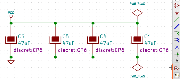
Power Symbols
Power symbols are symbols that are conventionally used to represent a connection to a power net, such as VCC or GND. In addition to being a visual indicator that the attached net is a power rail, power symbols make global connections: two power symbols with the same pin name connect to each other anywhere in the schematic, regardless of sheet.
Power symbols are virtual: they do not represent a physical component on the PCB.
In the figure below, power symbols are used to connect the positive and negative terminals of the capacitors to the VCC and GND nets, respectively.
In the KiCad standard library, power symbols are found in the power library, but power symbols can be created in any library.
To create a custom power symbol, make a new symbol with a power input pin that is set to be invisible. Name the pin according to the desired power net. In addition, set the "Define as power symbol" symbol property. As described in the hidden power pins section, invisible power input pins make global connections based on the hidden power pin’s name. The process of creating a power symbol is described in more detail in the Symbol Editor section.
| The connected net name is determined by the power symbol’s pin name, not the name or value of the symbol. This means that power symbol net names can only be changed in the symbol editor, not in the schematic. |
Net name assignment rules
Every net in the schematic is assigned a name, whether that name is specified by the user or automatically generated by KiCad.
When multiple labels are attached to the same net, the final net name is determined in the following order, from highest priority to lowest:
-
Etichette globali
-
Etichette locali
-
Etichette gerarchiche
-
Pin fogli gerarchici
If there are multiple labels of one type attached to a net, the names are sorted alphabetically and the first is used.
If a net travels through multiple sheets of a hierarchy, it will take its name from the highest level of the hierarchy where it has a hierarchical label or local label. As usual, local labels take priority over hierarchical labels.
If none of the label types above are attached to a net, the net’s name is automatically generated based on the connected symbol pins.
PWR_FLAG
Due simboli PWR_FLAG sono visibili nella schermata soprastante. Essi indicano all’ERC che le due net di potenza VCC e GND sono effettivamente connesse ad una sorgente di potenza, dato che non c’è una sorgente di potenza esplicita come l’uscita di un regolatore di tensione collegata a nessuno dei due collegamenti.
Without these two flags, the ERC tool would diagnose: Error: Input Power pin not driven by any Output Power pins.
The PWR_FLAG symbol is found in the power symbol library. The same effect can be achieved by connecting any power output pin to the net.
Indicatore di Non-connesso
No-connection flags (![]() ) are used to indicate that a pin is intentionally unconnected. These flags prevent "unconnected pin" ERC warnings for pins that are intentionally unconnected.
) are used to indicate that a pin is intentionally unconnected. These flags prevent "unconnected pin" ERC warnings for pins that are intentionally unconnected.
Note that no-connection flags are distinct from the "unconnected" symbol pin type, although they both prevent "unconnected pin" ERC warnings on the pin in question.
Netclasses
Netclasses are groups of nets that can be assigned design rules (for the PCB) and graphical properties (for the schematic). In KiCad, each net is part of exactly one net class. If you do not add a net to a specific class, it will be part of the Default class, which always exists.
Net classes may be created and edited in either the Schematic or Board Setup dialogs. Nets can be added to netclasses in either the schematic or board using pattern-based assignments described below. Nets can also be assigned to netclasses in the schematic using graphical assignments with net class directives or net labels.
Selecting a wire or label displays the net’s netclass in the message panel at the bottom of the window.
Managing netclasses in Schematic Setup
Netclasses are managed in the Net Classes panel of the Schematic Setup dialog.
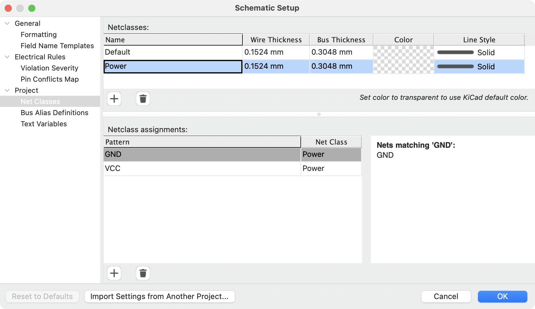
The top pane lists the netclasses that exist in the design. The Default netclass always exists, and you can add additional netclasses with the ![]() button or remove the selected netclass with the
button or remove the selected netclass with the ![]() button.
button.
Each netclass can have unique graphic properties that determine how wires of that netclass are displayed in the schematic. Wire and bus thicknesses, color, and line style (solid, dashed, dotted, etc.) can all be adjusted. Setting the color to transparent will use the theme’s default wire/bus color for the netclass, which is configurable in Preferences.
You can also set board design rules for each netclass, although the DRC fields are hidden by default. Right click the header row to show or hide additional columns. For more information about setting netclass design rules, see the PCB editor documentation.
The bottom pane lists pattern-based netclass assignments. Each row has a net name pattern and a netclass; nets with names that match the pattern are assigned to the specified netclass. If a net matches multiple patterns, the first match is used. Pattern-based netclass assignments are dynamic: when a new net is added that matches an existing pattern, it will be assigned to the associated netclass automatically. Net patterns can use both wildcards (* to match any number of any characters, including none, and ? to match any character) and regular expressions. The nets that match the selected pattern are displayed to the right of the pattern list.
For example, the net* pattern matches nets named net, net1, network, and any other net name beginning with net. Because * has a slightly different meaning in a regular expression (* matches zero or more of the preceding character), the net* pattern would also match a net named ne.
Remember that net names must include the full sheet path. For example, a
locally labeled net in the root sheet has a name prefixed with /.
|
Use the ![]() button to add a net class assignment pattern or the
button to add a net class assignment pattern or the ![]() button to remove a pattern.
button to remove a pattern.
A netclass pattern containing only the * wildcard will match all
explicitly named nets, but will not match unlabeled nets. To match
unlabeled nets, you can include more of the net name before the wildcard
character. All unlabeled nets have names that begin with Net-, so the
pattern Net-* will match all unlabeled nets. You can also assign a
netclass to an unlabeled net using a
net class directive.
|
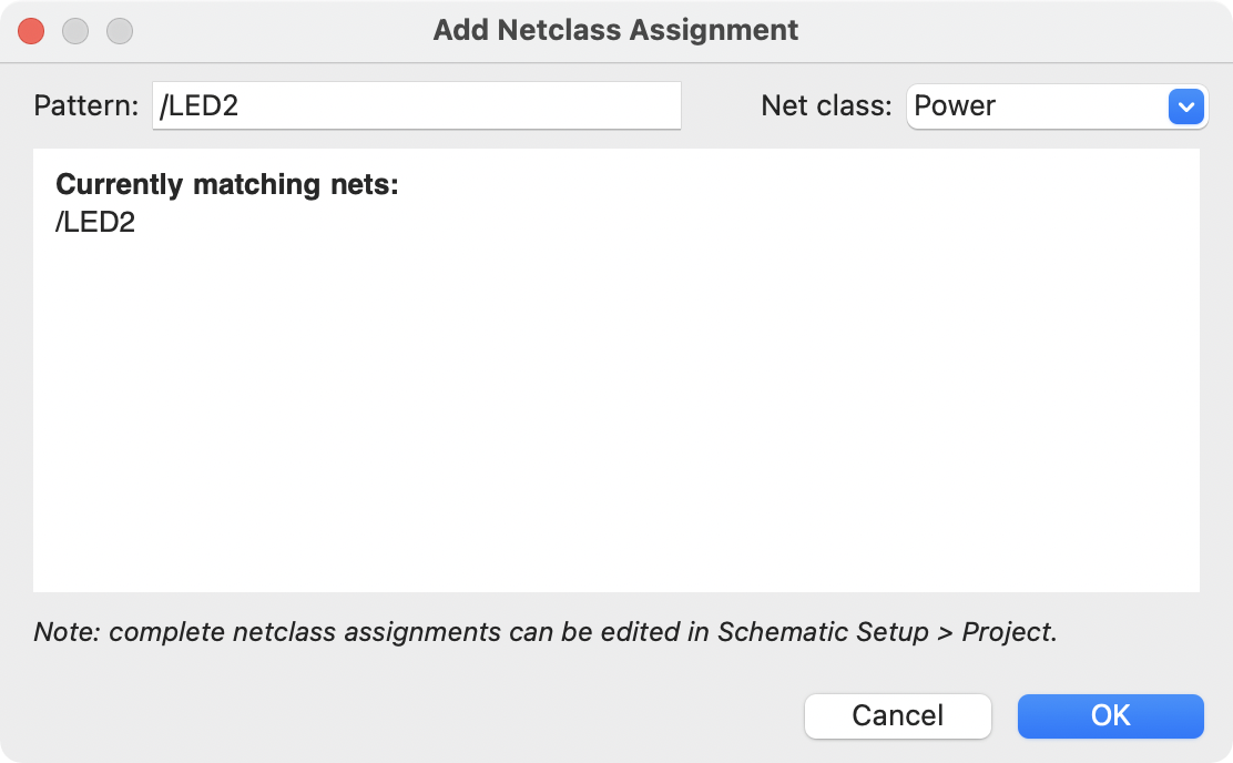
Instead of adding netclass patterns in the Schematic Setup dialog, you can directly create netclass patterns from the schematic canvas. Right click a net and select Assign Netclass… to bring up the Add Netclass Assignment dialog. The netclass pattern is pre-filled with the name of the selected net, but the pattern can be changed if desired. All nets matching the pattern are displayed in the dialog.
Graphically assigning netclasses in the schematic
As an alternative to pattern-based netclass assignment, netclasses can be graphically assigned to nets in the schematic using either net class directives or labels. Netclasses must be created in Schematic Setup before they can be assigned graphically.
In the image below, a net class directive is used to assign signals to the 50R netclass.
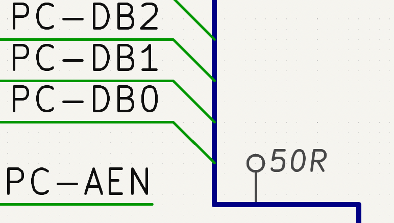
Net class directives are added with the ![]() button in the right toolbar. They behave like labels, except that they cannot be used to name a net. The attached net is assigned a netclass according to the value of the directive’s
button in the right toolbar. They behave like labels, except that they cannot be used to name a net. The attached net is assigned a netclass according to the value of the directive’s Net Class field. The Net Class field presents a dropdown list of all the net classes in the design.
If a directive is attached to a bus, all members of the bus are assigned to the specified net class.
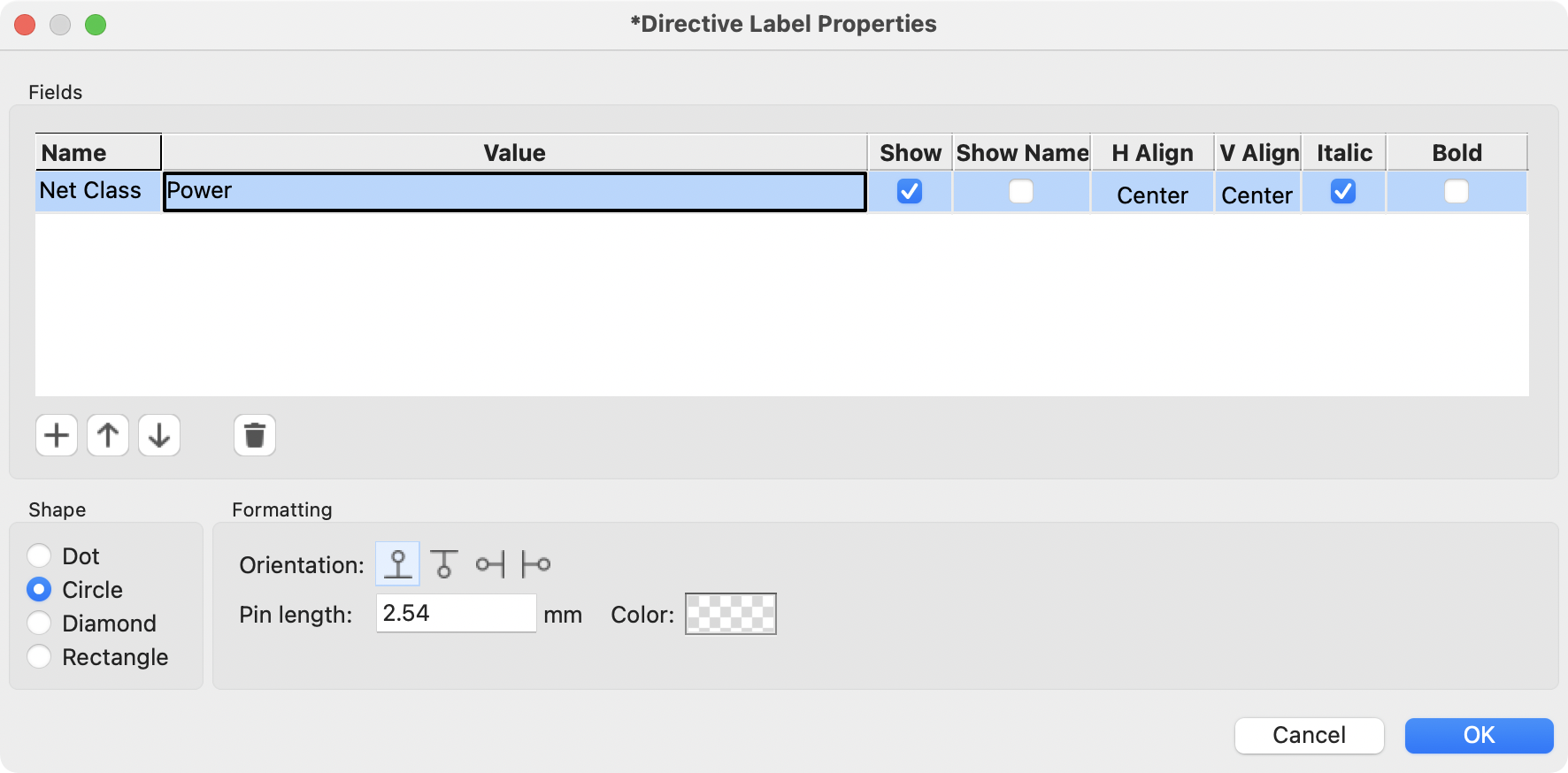
In addition to the associated netclass, you can edit the directive’s shape (dot, circle, diamond, or rectangle), orientation, pin length, and color in the directive’s properties.
Net labels can also be used to assign netclasses to nets by adding a Net Class field to the label.
If more than one different netclass is graphically assigned to a single net, ERC will report an issue. Graphical netclass assignments override pattern-based assignments: if a net matches a netclass pattern assignment and also has a netclass assigned graphically, the graphically assigned netclass will be used.
Elementi grafici
Text, graphic shapes, and images can be added to schematics for documentation purposes. These items do not have any electrical effect on the schematic.
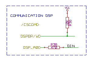
The image below shows graphic lines and text ("COMMUNICATION DSP") in addition to symbols and several types of labels.
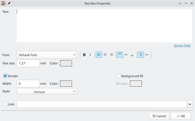
Text and Text Boxes
Two kinds of text can be added to schematics, which are referred to as text (![]() ) and text boxes (
) and text boxes (![]() ). Both are added using their respective buttons in the right toolbar.
). Both are added using their respective buttons in the right toolbar.
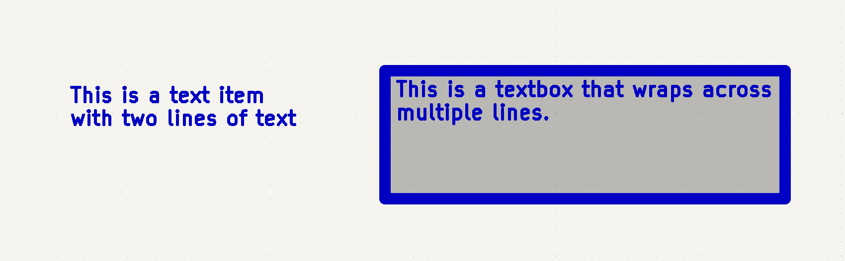
Both kinds of text item support multiline text and basic formatting features, but text boxes wrap text to fit in the outline and have additional formatting options. All text has adjustable fonts, color, size, bold and italic emphasis, left and right alignment, and vertical and horizontal orientation. Text boxes additionally support horizontal centering, vertical alignment options, and colored borders and fill.
| The default text size can be set for a schematic in Schematic Setup, and the default font can be set in Preferences. |
Links
Text and text boxes can be made into a link by entering a target in the Link box in the text properties. The link target can be a local file (using the file:// protocol prefix followed by the file’s path), to a website (using http:// or https:// followed by the rest of the URL), or to another page in the same schematic (using # followed by the page number). These can also be autofilled using the dropdown menu in the link target box.
Fonts
Text and text boxes support custom fonts, which are selectable with the Font dropdown in the properties dialog for the text. In addition to the KiCad font, you can use any TTF font installed on your computer.
| User fonts are not embedded in the project. If the project is opened on another computer that does not have the selected font installed, a different font will be substituted. For maximum compatibility, use the KiCad font. |
Text Markup
Text supports markup for superscripts, subscripts, overbars, evaluating project variables, and accessing symbol field values.
| Feature | Markup Syntax | Result |
|---|---|---|
Superscript |
|
textsuperscript |
Subscript |
|
textsubscript |
Overbar |
|
text |
|
variable_value |
|
|
field_value of symbol refdes |
| Variables must be defined in Schematic Setup before they can be used. There are also a number of built-in system text variables. |
Graphic Shapes
Graphic rectangles (![]() ), circles (
), circles (![]() ), arcs (
), arcs (![]() ), and lines (
), and lines (![]() ) can all be added using their respective buttons in the right toolbar.
) can all be added using their respective buttons in the right toolbar.
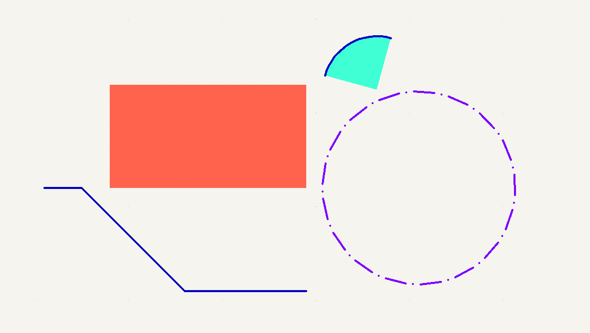
Line width, color, and style (solid, dashed, or dotted) can be configured in the properties dialog for each shape (E). Rectangles, circles, and arcs can also have a fill color set and have their outlines removed.
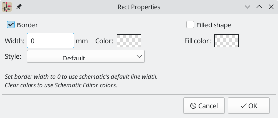
Setting a shape’s line width to 0 uses the schematic default line width, which is configurable in Schematic Setup. Spacing for line dashes is also configurable there. Removing a line or fill color uses the color theme’s graphics color, which is configurable in Preferences.
Like wires, graphic lines obey the line drawing mode setting (90 degree, 45 degree, or free angle), which you can set using the toggle buttons on the left toolbar (![]() ,
, ![]() , and
, and ![]() , respectively). Shift+Space cycles through the modes.
, respectively). Shift+Space cycles through the modes.
As with PCB tracks, the / hotkey switches line posture.
Bitmap Images
Bitmap images can be added to the schematic with the ![]() button. Images in the schematic can be moved and scaled. The properties dialog allows setting a location and scale as well as converting the image to greyscale.
button. Images in the schematic can be moved and scaled. The properties dialog allows setting a location and scale as well as converting the image to greyscale.
Bulk editing text and graphics
Properties of text and graphics can be edited in bulk using the Edit Text and Graphic Properties dialog (Tools → Edit Text and Graphic Properties…). The tool can also modify visual properties of wires and buses.
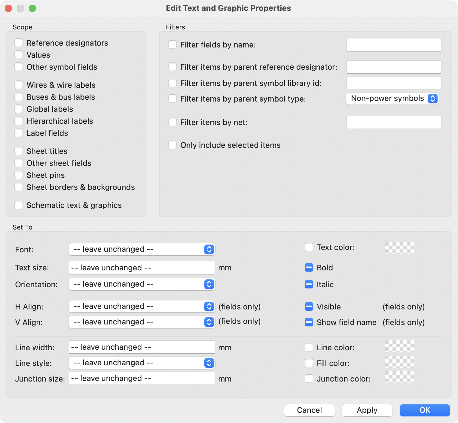
Scope and Filters
Scope settings restrict the tool to editing only certain types of objects. If no scopes are selected, nothing will be edited.
Filters restrict the tool to editing particular objects in the selected scope.
Objects will only be modified if they match all enabled and relevant filters
(some filters do not apply to certain types of objects. For example, symbol
field filters do not apply to wires and are ignored for the purpose of changing
wire properties). If no filters are enabled, all objects in the selected scope
will be modified. For filters with a text box, wildcards are supported: *
matches any number of any characters, including none, and ? matches any single
character.
Filter fields by name filters to the specified symbol, label, or sheet field.
Filter items by parent reference designator filters to fields in the symbol with the specified reference designator. Filter items by parent symbol library id filters to fields in symbols with the specified library identifier. Filter items by parent symbol type filters to fields in symbols of the selected type (power or non-power).
Filter items by net filters to wires and labels on the specified net.
Only include selected items filters to the current selection.
Editable Properties
Properties for filtered objects can be set to new values in the bottom part of the dialog.
Drop-down lists and text boxes can be set to -- leave unchanged -- to preserve existing values. Checkboxes can be checked or unchecked to enable or disable a change, but can also be toggled to a third "leave unchanged" state. Color properties must be checked to change the value; a checkerboard swatch indicates that the color will be inherited from the default value from the the schematic settings or netclass properties.
Text properties that can be modified are font, text size, text orientation (right/up/leftdown), horizontal and vertical alignment, text color, emphasis (bold and italic), and visibility of fields and field names.
Graphic and wire properties that can be modified are line width, line style (solid, dashed, and dotted lines), line color, fill color for shapes, and junction size and junction color for wire junctions.
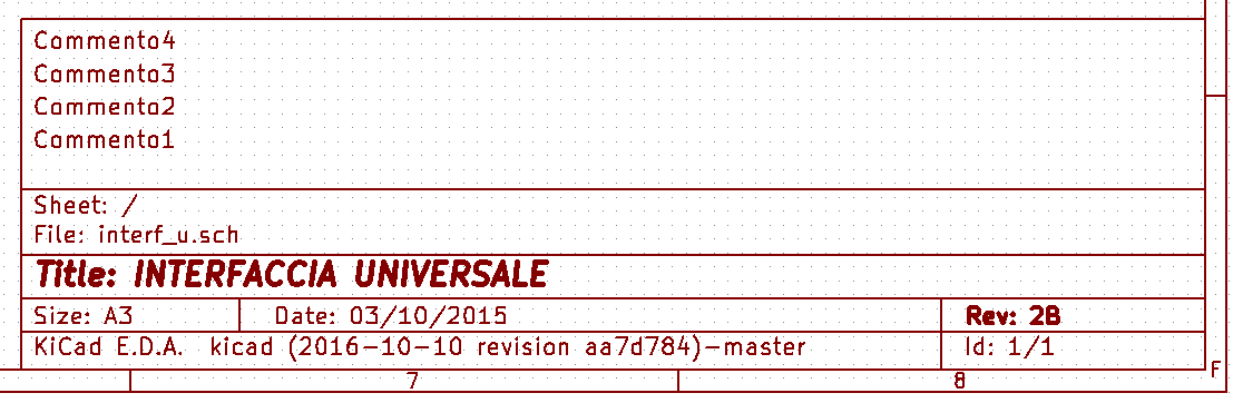
Blocco del titolo del foglio
Il riquadro iscrizioni viene modificato con lo strumento per le inpostazioni pagina (![]() ).
).
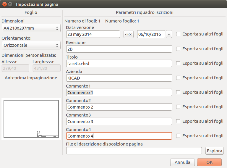
Each field in the title block can be edited, as well as the paper size and orientation. If the Export to other sheets option is checked for a field, that field will be updated in the title block of all sheets, rather than only the current sheet.
You can set the date to today’s or any other date by pressing the left arrow button next to Issue Date. Note that the date in the schematic will not be automatically updated.
A drawing sheet template file can also be selected.
The sheet number (Sheet X/Y) is automatically updated, but sheet page numbers can also be manually set using Edit → Edit Sheet Page Number….
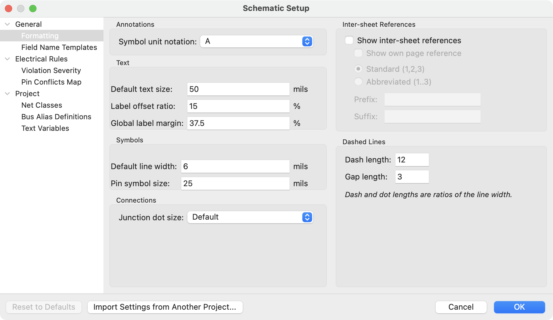
Impostazioni schema
La finestra Impostazioni schema viene utilizzata per impostare le opzioni dello schema che sono specifiche dello schema attualmente attivo. Ad esempio, la finestra contiene le opzioni di formattazione, la configurazione delle regole elettriche, l’impostazione della netclass e l’impostazione delle variabili di testo dello schema.
You can import schematic settings from an existing project using the Import Settings from Another Project… button. This allows you to choose a project to use as a template and select which settings to import (formatting preferences, field name templates, pin conflict map, violation severities, and net classes).
Schematic formatting
The formatting panel contains settings for the appearance of symbols, text, labels, graphics, and wires.
Symbol unit notation sets how each unit of a multi-unit symbol is referred to
in its reference designator. By default, a different letter for each unit is
appended to the reference designator with no separator, for example U1B for
the second unit of symbol U1, but this can be changed. Numbers can be used
instead of letters, and various separators can be used between the symbol
designator and the unit identifier (., -, _, or none).
Default text size sets the default text height used by the text, text box, and
label tools. Label offset ratio controls the vertical spacing between a local
label’s text and the attached wire, relative to the label’s text size. This also
affects the spacing between symbol pins and their pin number.
Global label margin defines the size of the box around a global label,
relative to the global label’s text size. Increasing the margin may be useful
to avoid overlapping text with overbars (~{}) or letters with descenders, but
this may cause closely packed global labels to overlap with each other.
Default line width sets the default line width for symbol graphics, if the symbol does not override the default line width. Pin symbol size scales symbol pin graphic style annotations, such as the bubble on an inverted pin.
Junction dot size sets the schematic’s default wire junction dot size. The default size can be overridden by editing an individual junction dot’s properties.
Show inter-sheet references enables or disables the display of
inter-sheet references, which are a list of page
numbers next to a global labels that link to other places in the schematic where
the same global label appears. Show own page reference controls whether the
current page is included in the list of page numbers. Standard and
abbreviated determine whether to display the complete list of page numbers or
only the first and last page numbers. The prefix and suffix fields add
optional characters before and after the list of page numbers. In the image
of an inter-sheet reference below, a prefix and suffix of [ and ],
respectively, have been added.
Dashed line appearance is controlled in the Formatting section. Dash length controls the length of dashes, while Gap length controls the spacing between dashes and dots. The dash and gap lengths are relative to the line width: a gap length of 2 means twice the width of the line.
Field name templates
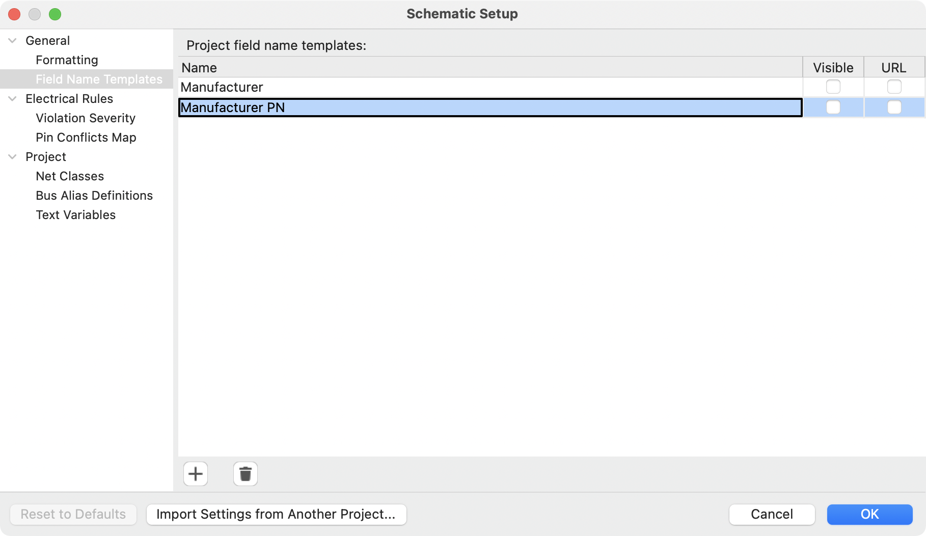
Field name templates are empty symbol fields that are automatically added to all symbols in the schematic. These can be useful when every symbol in the schematic needs additional fields beyond the fields that are defined in the library symbols, for example a field for the manufacturer’s part number.
Template fields can be set as visible or invisible, and can also be set as URL fields.
Field name templates that are defined in schematic setup apply only to the current project. Field name templates can also be defined in Preferences, which apply to all projects edited on your computer.
ERC violation severity and pin conflicts map
The Violation Severity panel lets you configure what types of ERC messages should be reported as Errors, Warnings, or ignored.
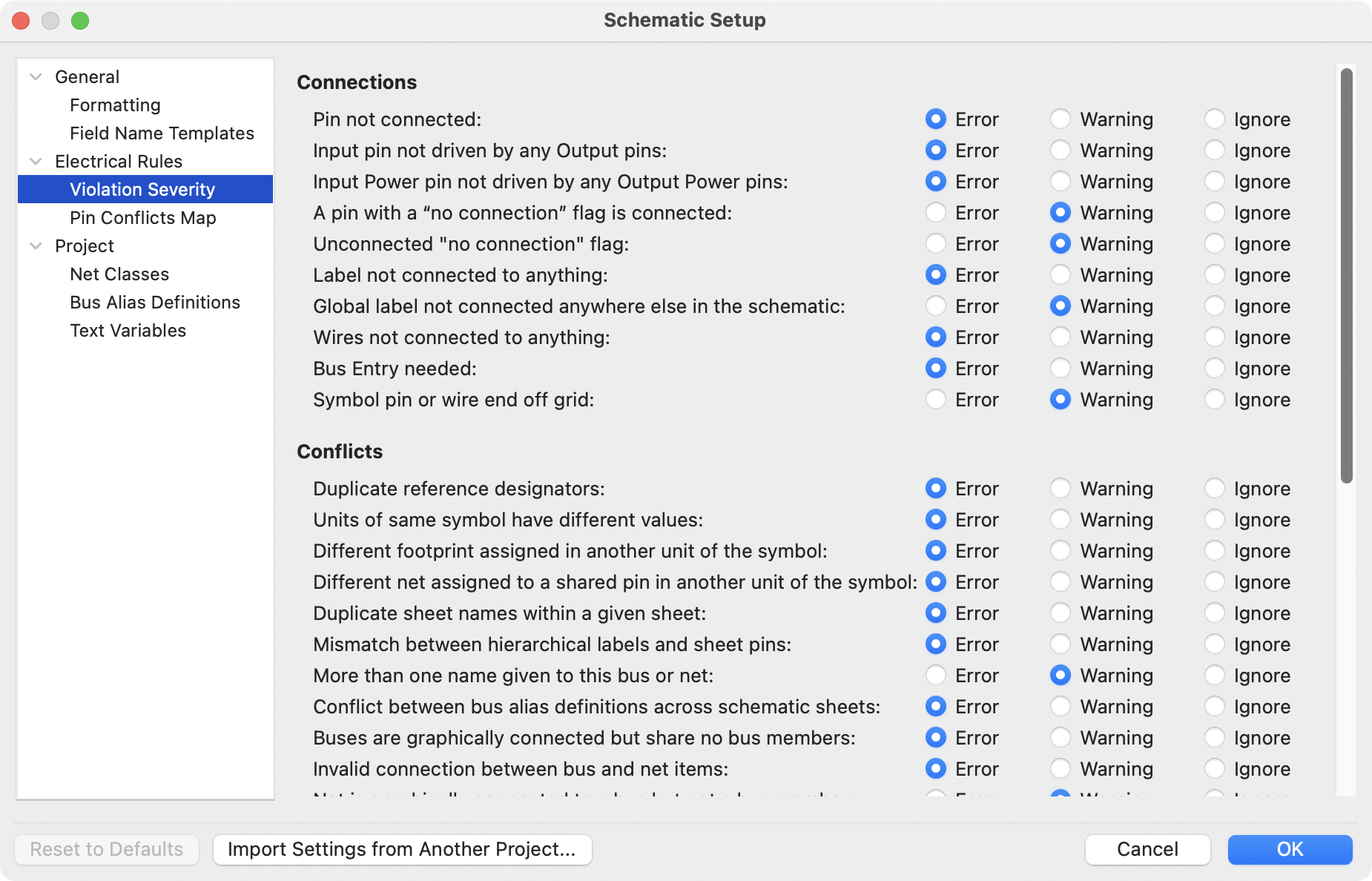
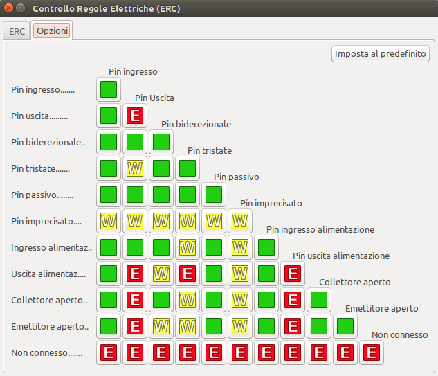
The Pin Conflicts Map allows you to configure connectivity rules to define electrical conditions for errors and warnings based on what types of pins are connected to each other. For example, by default an error is produced when an output pin is connected to another output pin.
These panels are explained in more detail in the ERC section.
Net classes
The Net Classes panel allows you to manage netclasses for the project and assign nets to netclasses with patterns. Managing netclasses in this panel is equivalent to managing them in the Board Setup dialog. Nets can also be assigned to netclasses in the schematic using graphical assignments with net class directives or net labels.
Pattern-based netclass assigment is explained in more detail in the net classes section.
Bus alias definitions
The Bus Alias Definitions panel allows you to create bus aliases, which are names for groups of signals in a bus. For more information about bus aliases, see the bus alias documentation.
Variabili di testo
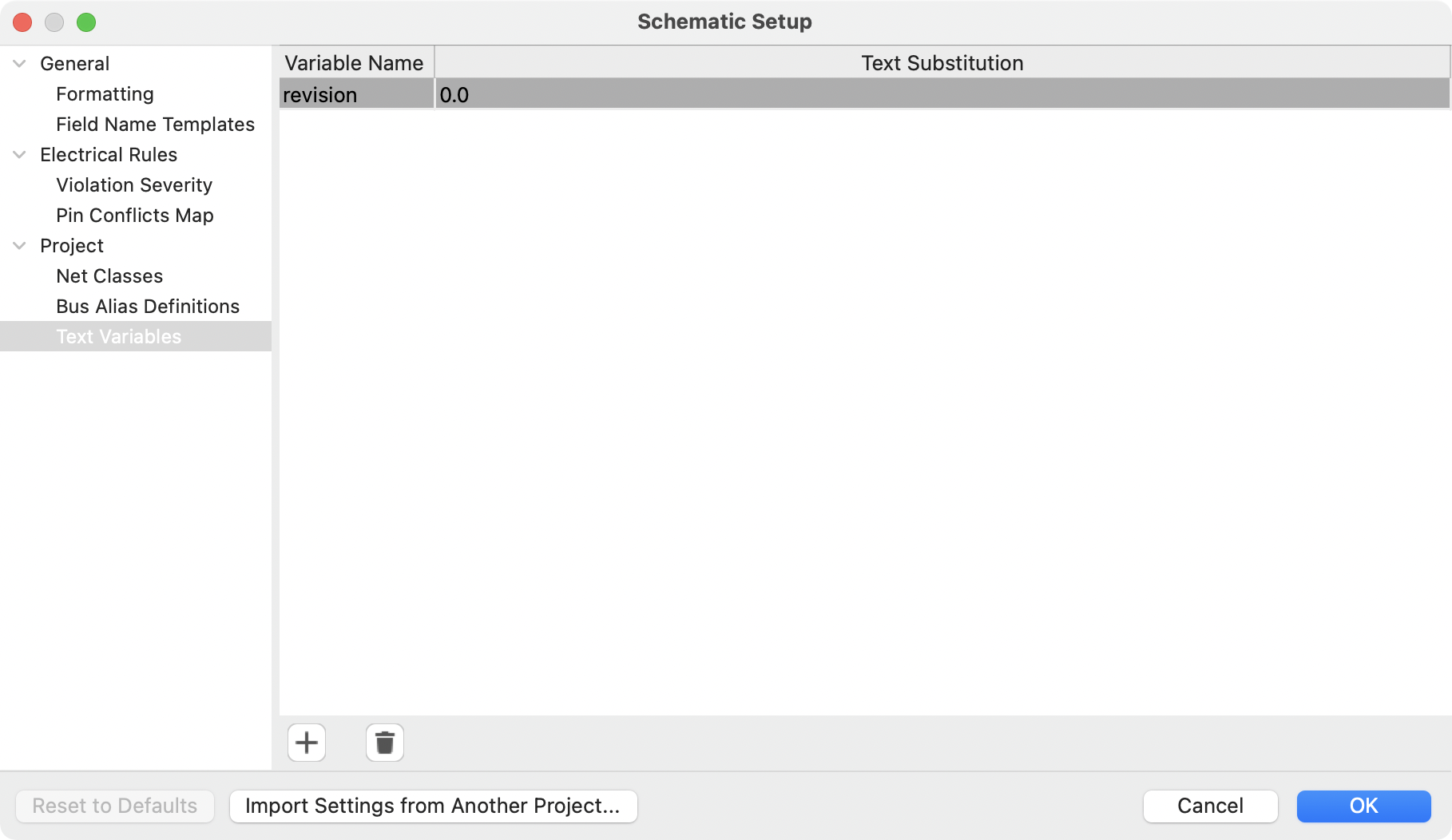
Text replacement variables can be created in the Text Variables section. These variables allow you to substitute the variable name for any text string. This substitution happens anywhere the variable name is used inside the variable replacement syntax of ${VARIABLENAME}.
For example, you could create a variable named VERSION and set the text substitution to 1.0. Now, in any text object on the PCB, you can enter ${VERSION} and KiCad will substitute 1.0. If you change the substitution to 2.0, every text object that includes ${VERSION} will be updated automatically. You can also mix regular text and variables. For example, you can create a text object with the text Version: ${VERSION} which will be substituted as Version: 1.0.
Text variables can also be created in Board Setup. Text variables are project-wide; variables created in the schematic editor are also available in the board editor, and vice versa.
There are also a number of built-in system text variables.
Opening legacy schematics
Modern versions of KiCad can always open projects created in older versions of KiCad. However, schematics created in some older versions of KiCad have special considerations that must be observed when opening them in order to prevent any data loss.
Opening KiCad 5.0 and 5.1 schematics
Modern versions of KiCad can open schematics created in versions prior to KiCad 6.0, but the cache library file (<projectname>-cache.lib) must be present to load the schematic correctly.
Since version 6.0, KiCad stores all symbols used in a project in the schematic. This means that you can open a schematic made in KiCad 6.0 or later on any computer, even if the libraries used in the project are not installed or have changed. Modern KiCad schematic files use the .kicad_sch extension.
Prior to version 6.0, KiCad did not store symbols in the schematic. Instead, KiCad stored references to the symbols and their libraries. It also stored a copy of every symbol used by the project in a separate cache library file (<projectname>-cache.lib). As long as the cache library was included with the project, the project could be distributed without the system library files, because KiCad could load any needed symbols from the cache library as a fallback if the libraries referenced in the schematic were missing. Legacy KiCad schematic files use the .sch extension.
When you open a legacy schematic, KiCad will look in the cache library to find all of the symbols used in the schematic in the cache library. When you save the legacy schematic, KiCad will save it as a new file in the modern schematic format (.kicad_sch), with the necessary symbols embedded in the schematic itself. The original legacy schematic and the cache library will remain, unmodified, but they are no longer necessary once the schematic has been saved in the modern format.
| Projects created in KiCad prior to version 6.0 must have a cache library. If the cache library is missing, the schematic will lose symbol information if the system symbol libraries are modified, reorganized, moved, or deleted. The libraries included with legacy versions of KiCad are substantially different than the modern KiCad libraries, so in practice KiCad will almost always fail to open legacy projects unless the cache library is present. |
When you open a legacy schematic, KiCad may display the Project Rescue Helper dialog. This means that one or more symbols in the cache library do not match the corresponding symbol in the external library. The dialog helps you "rescue" symbols from the cache library into your schematic, if desired. You can also open the rescue dialog at any time using Tools → Rescue Symbols…. The cache library file must be present in order to use the rescue tool.
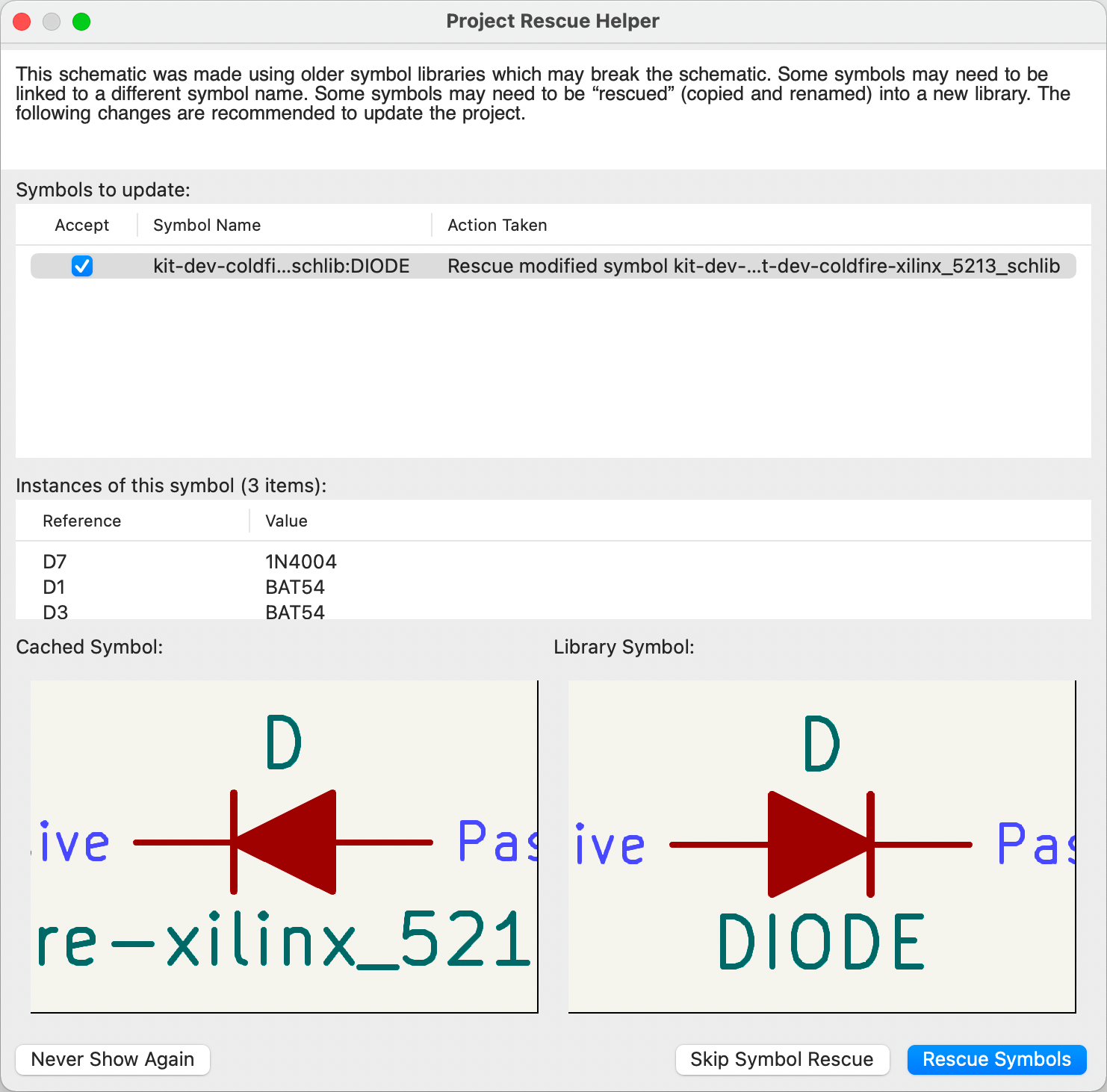
The rescue dialog lists all symbols that don’t match between the cache library and the external symbol library. The discrepancy can be because:
-
the cached symbol or the library symbol has been modified, so the two symbols no longer match, or
-
the cached symbol does not have a corresponding symbol in the symbol library, because the symbol or library was moved, renamed, deleted, or is not present on the current computer.
For each symbol in the list, selecting the symbol displays the reference designator and value for each instance of the symbol, and shows a visual preview of the symbol. If a corresponding symbol exists in the system symbol library, the dialog shows both copies of the symbol for comparison. If the symbol only exists in the cache library, the dialog only shows the cached symbol.
In this example, the project originally used a diode with the cathode facing left, but the library now contains one with the cathode facing right. This change would break the design, so it would be important to use the cached symbol as the original designer intended.
Pressing Rescue Symbols here will cause the selected symbols from the cache library to be saved into a special rescue library (<projectname>-rescue.kicad_sym). The corresponding symbols in the schematic will be updated to use the newly rescued symbols. Any unselected symbols will not be rescued, but their symbol linkage can be updated in the schematic later.
Alternatively, pressing Skip Symbol Rescue will exit the dialog without rescuing any symbols. KiCad will use the versions of the symbols found in the external libraries. You can run the rescue function again with Tools → Rescue Symbols…, or manually edit symbol linkage in the symbol’s properties.
If you would prefer not to see this dialog, you can press Never Show Again. This has the same effect as pressing Skip Symbol Rescue for the current schematic and all future schematics.
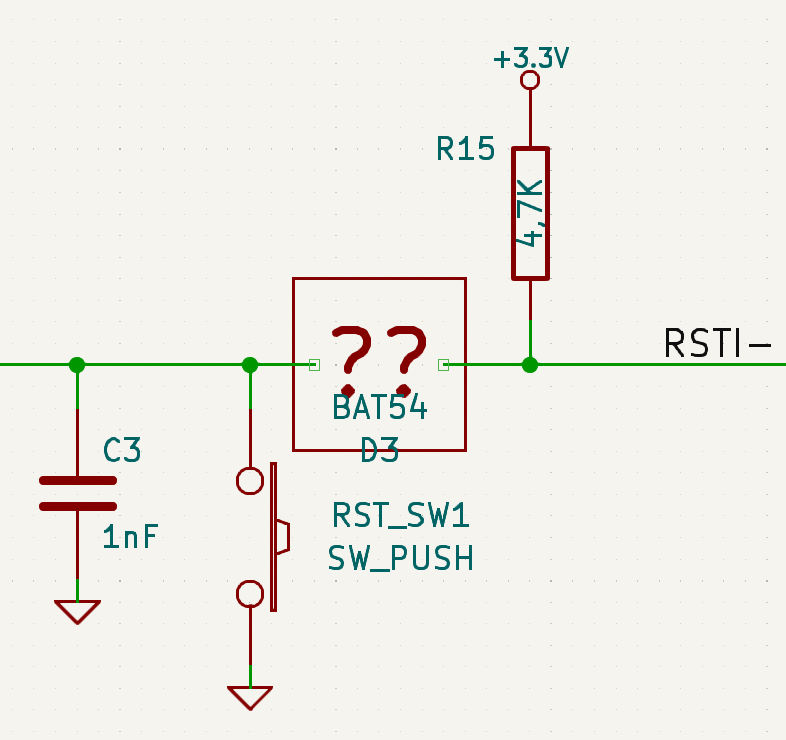
If a symbol in a legacy schematic cannot be found in either the cache library or the external library, KiCad cannot rescue that symbol. A placeholder symbol is inserted into the schematic in its place, as shown below.
You can attempt to remap these orphaned symbols using the Change Symbols or Edit Symbol Library Links dialogs, but either option may require manual corrections to the schematic. These tools are explained in more detail in the Updating and exchanging symbols section.
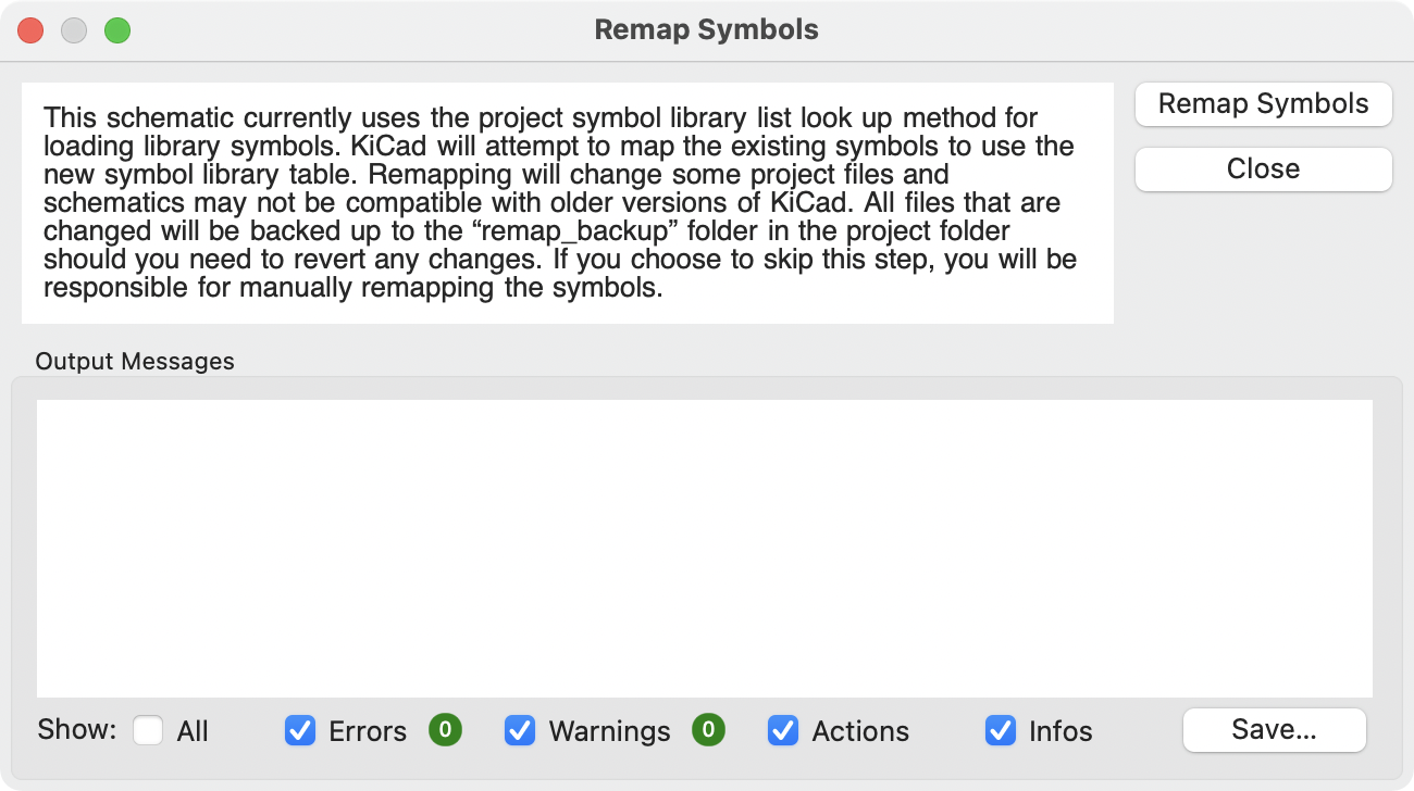
Opening pre-5.0 schematics
Modern versions of KiCad can open schematics created in versions prior to KiCad 5.0, but you will need to go through a symbol remapping process to open the schematic without losing symbol information.
Since version 5.0, KiCad schematics refer to specific symbols using both the symbol and library name. Even if multiple libraries each contain a symbol with the same name, the designer’s intended symbol is unambiguously specified.
Prior to version 5.0, KiCad schematics stored only the symbol name, not the library name. Symbols in the schematic were indirectly mapped back to the original library by searching through the project’s library list for a matching symbol. When you open a pre-5.0 schematic, KiCad will attempt to automatically "remap" the symbols so that each bare symbol name is replaced with a fully-specified symbol library and symbol name pair. The original schematics will be backed up in a rescue-backup folder.
You can skip the automatic remapping, but you will need to remap the symbols yourself using the Change Symbols dialog. You can also re-run the Remap Symbols tool using Tools → Remap Legacy Library Symbols….