Inspecting a board
Measurement tool
The measurement tool allows you to make distance and angle measurements between points on the PCB. To activate the tool, click the ![]() icon in the right toolbar, or use the hotkey Ctrl+Shift+M. Once the tool is active, click once to set the measurement start point, then click again to finish a measurement.
icon in the right toolbar, or use the hotkey Ctrl+Shift+M. Once the tool is active, click once to set the measurement start point, then click again to finish a measurement.
| The measurement tool is used for quick measurements that do not need to be displayed permanently. Any measurement you make will only be shown while the tool is active. To create permanent dimensions that will appear in printouts and plots, use the Dimension tools. |
Design rule checking
The design rule checker is used to verify that the PCB meets all the requirements established in the Board Setup dialog and that all pads are connected according to the netlist or schematic. KiCad can automatically prevent some design rule violations while routing tracks, but many others cannot be prevented automatically. This means it is important to use the design rule checker before creating manufacturing files for a PCB.
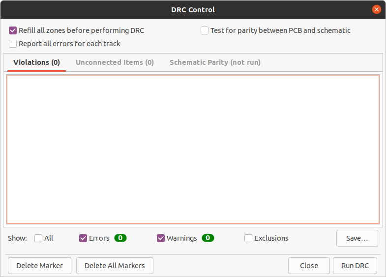
To use the design rule checker, click the ![]() icon in the top toolbar, or select Design Rules Checker from the Inspect menu.
icon in the top toolbar, or select Design Rules Checker from the Inspect menu.
The top section of the DRC Control window contains some options that control the design rule checker:
Refill all zones before performing DRC: when enabled, zones will be refilled every time the design rule checker is run. Disabling this option may result in incorrect DRC results if zones have not been refilled manually.
Report all errors for each track: when enabled, all clearance errors will be reported for each track segment. When disabled, only the first error will be reported. Enabling this option will result in the design rule checker running more slowly.
Test for parity between PCB and schematic: when enabled, the design rule checker will test for differences between the schematic and PCB in addition to testing the PCB design rules. This option has no effect when running the PCB editor in standalone mode.
After running DRC, any violations will be shown in the center part of the DRC Control window. Rule violations, unconnected items, and differences between the schematic and the PCB are shown in three different tabs. The controls below the list of violations can be used to show or hide violations depending on their severity. A report file in plain text format can be created after running DRC using the Save button.
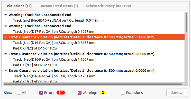
Each violation involves one or more object on the PCB. In the list of violations, the objects involved are listed below the violation. Clicking on the violation in the list view will move the PCB Editor view so that the affected area is centered. Clicking on one of the objects involved in a violation will highlight the object.
Right-clicking a violation in the list view will open a context menu with additional actions including excluding the selected violation. Excluded violations are hidden unless the Exclusions checkbox is enabled at the bottom of the DRC Control window. Excluded violations are remembered between runs of the design rule checker.
Clearance and constraint resolution
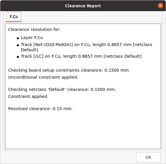
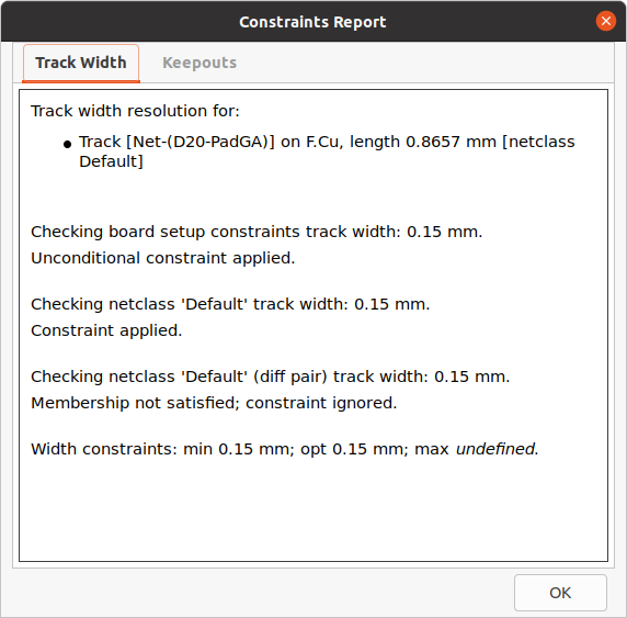
The clearance and constraint resolution tools allow you to inspect which clearance and design constraint rules apply to selected items. These tools can help when designing PCBs with complex design rules where it is not always clear which rules apply to an object.
To inspect the clearance rules that apply between two objects, select both objects and choose Clearance Resolution from the Inspect menu. The Clearance Report dialog will show the clearance required between the objects on each copper layer, as well as the design rules that resulted in that clearance.
To inspect the design constraints that apply to an object, select it and choose Constraints Resolution from the Inspect menu. The Constraints Report dialog will show any constraints that apply to the object.
Find tool
The Find tool searches for text in the PCB, including reference designators, footprint fields, and graphic text. When the tool finds a match, the canvas is zoomed and centered on the match and the text is highlighted. Launch the tool using the (![]() ) button in the top toolbar.
) button in the top toolbar.
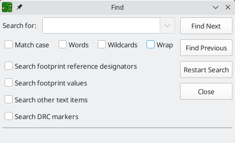
The Find tool has several options:
Match case: Selects whether the search is case-sensitive.
Words: When selected, the search will only match the search term with complete words in the PCB. When unselected, the search will match if the search term is part of a larger word in the PCB.
Wildcards: When selected, wildcards can be used in the search terms. ?
matches any single character, and * matches any number of characters. Note
that when this option is selected, partial matches are not returned: searching
for abc* will match the string abcd, but searching for abc will not.
Wrap: When selected, search results will return to the first hit after reaching the last hit.
Search footprint reference designators: Selects whether the search should apply to footprint reference designators.
Search footprint values: Selects whether the search should apply to footprint value fields.
Search other text items: Selects whether the search should apply to other text items, including graphical text and footprint fields other than value and reference.
Search DRC markers: Selects whether the search should apply to the violation descriptions of DRC markers shown on the board.
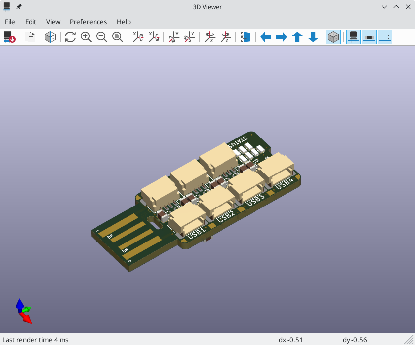
Visualizzatore 3D
The 3D Viewer shows a 3-dimensional view of the board and the components on the board. You can view the board from different perspectives, show or hide different types of components, cross-probe from the PCB Editor to the 3D viewer, and generate raytraced renders of the board.
| The 3D model for a component will only appear if the 3D model file exists and has been assigned to the footprint. |
| Many footprints in KiCad’s standard library do not yet have model files created for them. However, these footprints may contain a path to a 3D model that does not yet exist, in anticipation of the 3D model being created in the future. |
Navigating the 3D view
Dragging with the left mouse button will orbit the 3D view around the centroid of the board. Scrolling the mouse wheel will zoom the view in or out. Scrolling while holding Ctrl pans the view left and right, and scrolling while holding Shift pans up and down. Dragging with the middle mouse button also pans the view.
Different sized 3D grids can be set using the Preferences → 3D Grid menu. Bounding boxes for each component can be enabled with Preferences → Show Model Bounding Boxes.
When the PCB Editor and the 3D Viewer are both open, selecting a footprint in the PCB Editor will also highlight the component in the 3D Viewer. The highlight color is adjustable in Preferences → Preferences… → 3D Viewer → Realtime Renderer → Selection Color.
Generating images with the 3D Viewer
The current 3D view can be saved to an image with File → Export Current View as PNG… or Export Current View as JPG…, depending on the desired image format. The current view can also be copied to the clipboard using the ![]() button, or Edit → Copy 3D Image.
button, or Edit → Copy 3D Image.
The 3D Viewer has a raytracing rendering mode which displays the board using a more physically accurate rendering model than the default rendering mode. Raytracing is slower than the default rendering mode, but it can be used when the most visually attractive results are desired. Raytracing mode is enabled with the ![]() button, or with Preferences → Raytracing. The 3D grid and selection highlights are not shown in raytracing mode.
button, or with Preferences → Raytracing. The 3D grid and selection highlights are not shown in raytracing mode.
Colors and other rendering options, for both raytraced and non-raytraced modes, can be adjusted in Preferences → Preferences… → 3D Viewer.
3D viewer controls
Many viewing options are controlled with the top toolbar.
|
Reload the 3D model |
|
Copy 3D image to clipboard |
|
Render current view using raytracing |
|
Zoom in |
|
Zoom out |
|
Redraw |
|
Fit drawing in display area |
|
Rotate X clockwise |
|
Rotate X counterclockwise |
|
Rotate Y clockwise |
|
Rotate Y counterclockwise |
|
Rotate Z clockwise |
|
Rotate Z counterclockwise |
|
Flip board view |
|
Pan board left |
|
Pan board right |
|
Pan board up |
|
Pan board down |
|
Enable/disable orthographic projection |
|
Show/hide 3D models for through-hole components |
|
Show/hide 3D models for surface mount components |
|
Show/hide 3D models for components of type 'other' |
Net inspector
The Net Inspector allows you to view statistics about all the nets in a board. To open the inspector, click the ![]() icon at the top of the Nets section of the Appearance panel, or select Net Inspector from the Inspect menu.
icon at the top of the Nets section of the Appearance panel, or select Net Inspector from the Inspect menu.
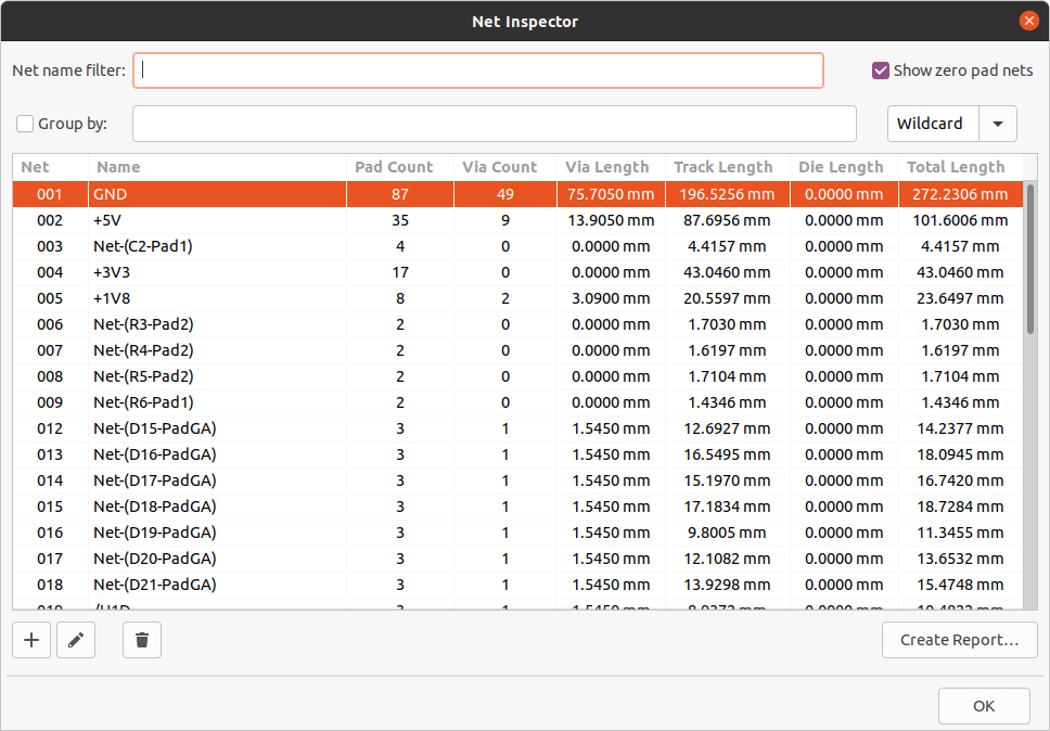
Clicking a net in the list will highlight that net on the board. Clicking a column title allows you to sort the list of nets by that column.
The Group By field allows you to combine different nets together and view the total length of the combined nets. For example, if you have two nets named DATA0 and DATA0_EXT, using a Group By value of DATA0* will create a group containing both nets. More complicated groupings can be created by changing the Group By mode from Wildcard to RegEx (regular expressions). The substring (Substr) variants of the Group By mode will create groups for each set of nets that matches the pattern differently.
For example, if you have the nets U1D+, U1D-, U2D+, and U2D-, the grouping pattern U*D will match all four nets in Wildcard mode, creating a single group U*D. In Wildcard Substr mode, it will match all four nets, but create two different groups: U1D and U2D.
Pad Count and Via Count show the number of pads (surface mount and through hole) and vias on a net. Via Length shows the total height of each via (not accounting for which copper layers the via connects to). In other words, Via Length is equal to Via Count multiplied by the stackup height of the board. Track Length shows the total length of all track segments in a net, not accounting for topology. Die length shows the total of all Pad to Die Length values set for pads on the net.
| The lengths shown in the Net Inspector differ from those shown in the length tuning tools, because the Net Inspector shows the sum of all tracks connected to a net, and the length tuning tools show the distance between the closest two pads or branching vias. See the Routing section for more information about the length tuner. |