Creación y Edición de Esquemas
Introducción
A schematic designed with KiCad is more than a simple graphic representation of an electronic device. It is normally the entry point of a development chain that allows for:
-
Validar una serie de reglas (Comprobador de Reglas Eléctricas) para detectar errores y omisiones.
-
Automatically generating a bill of materials.
-
Generando netlist parar software de simulación como SPICE
-
Defining a circuit for transferring to PCB layout.
A schematic mainly consists of symbols, wires, labels, junctions, buses and power symbols. For clarity in the schematic, you can place purely graphical elements like bus entries, comments, and polylines.
Symbols are added to the schematic from symbol libraries. After the schematic is made, the set of connections and footprints is imported into the PCB editor for designing a board.
Schematics can be contained in a single sheet or split among multiple sheets. In KiCad, multi-sheet schematics are organized hierarchically, with a root sheet and sub-sheet(s). Each sheet is its own .kicad_sch file and is itself a complete KiCad schematic. Working with hierarchical schematics is described in the Hierarchical Schematics chapter.
Schematic editing operations
Schematic editing tools are located in the right toolbar. When a tool is activated, it stays active until a different tool is selected or the tool is canceled with the Esc key. The selection tool is always activated when any other tool is canceled.
|
Selection tool (the default tool) |
|
Highlight a net by marking its wires and net labels with a different color. If the PCB Editor is also open then copper corresponding to the selected net will be highlighted as well. Net highlighting can be cleared by clicking with the highlight tool in an empty space, or by using the Clear Net Highlighting hotkey (~). |
|
Display the symbol selector dialog to place a new symbol. |
|
Display the power symbol selector dialog to place a new power symbol. |
|
Draw a wire. |
|
Draw a bus. |
|
Draw wire-to-bus entry points. These elements are only graphical and do not create a connection, thus they should not be used to connect wires together. |
|
Place a "no-connection" flag. These flags should be placed on symbol pins which are meant to be left unconnected. "No-connection" flags indicate to the Electrical Rule Checker that the pin is intentionally unconnected and not an error. They also affect schematic connectivity for stacked symbol pins. |
|
Place a junction. This connects two crossing wires or a wire and a pin, which can sometimes be ambiguous without a junction (i.e. if a wire end or a pin is not directly connected to another wire end). |
|
Place a local label. Local labels connect items located in the same sheet. For connections between two different sheets, use global or hierarchical labels. |
|
Place a net class directive label. |
|
Place a global label. All global labels with the same name are connected, even when located on different sheets. |
|
Place a hierarchical label. Hierarchical labels are used to create a connection between a subsheet and the sheet’s parent sheet. See the Hierarchical Schematics section for more information about hierarchical labels, sheets, and pins. |
|
Place a hierarchical subsheet. You must specify the file name for this subsheet. |
|
Import a hierarchical pin from a subsheet. This command can be executed only on hierarchical subsheets. It will create hierarchical pins corresponding to hierarchical labels placed in the target subsheet. |
|
Place a text comment. |
|
Place a text box. |
|
Draw a rectangle. |
|
Draw a circle. |
|
Draw an arc. |
|
Draw a graphic lines. Note: Lines are graphical objects and are not the same as wires placed with the Wire tool. They do not connect anything. |
|
Place a bitmap image. |
|
Delete clicked items. |
Grids and snapping
Schematic elements such as symbols, wires, text, and graphic lines are snapped to the grid when moving, dragging, and drawing them. Additionally, the wire tool snaps to pins even when grid snapping is disabled.
Both grid and pin snapping can be disabled while moving the mouse by using the modifier keys in the table below.
| On Apple keyboards, use the Cmd key instead of Ctrl. |
| Modifier Key | Effect |
|---|---|
Ctrl |
Disable grid snapping. |
Shift |
Disable snapping wires to pins. |
The default grid size is 50 mil (0.050") or 1.27 millimeters. This is the recommended grid for placing symbols and wires in a schematic and for placing pins when designing a symbol in the Symbol Editor. Smaller grids can also be used, but this is intended only for text and symbol graphics, and not recommended for placing pins and wires.
| Wires connect with other wires or pins only if their ends coincide exactly. Therefore it is very important to keep symbol pins and wires aligned to the grid. It is recommended to always use a 50 mil grid when placing symbols and drawing wires because the KiCad standard symbol library and all libraries that follow its style also use a 50 mil grid. Using a grid size other than 50 mil will result in schematics without proper connectivity! |
| Symbols, wires, and other elements that are not aligned to the grid can be snapped back to the grid by selecting them, right clicking, and clicking Align Elements to Grid. |
You can adjust the grid size by right-clicking and selecting a new grid from the list in the Grid submenu. Pressing the n or N hotkeys will cycle to the next and previous grid in the list, respectively.
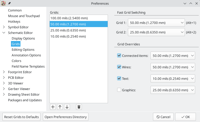
You can also select a new grid or edit the available grids in the Grids pane of the preferences dialog. As a shortcut to reach this dialog, right click the ![]() button on the left toolbar and select Edit Grids….
button on the left toolbar and select Edit Grids….
In this dialog you can select an active grid from the list of grids, reorder the list of grids, and add or remove grids. Grids defined in this dialog can have unequal X and Y spacing as well as an optional name.
This dialog also lets you designate two grids from the list as "Fast Grids", which can be quickly selected using Alt+1 and Alt+2.
Finally, you can configure grid overrides for different types of objects. Grid overrides let you set particular grid sizes for different types of objects which will be used instead of the default grid when working with those objects. For example, you can set a 50 mil grid for wires and connected items while using smaller grids to finely position text and graphics. Grid overrides can be individually enabled and disabled in this dialog, or globally enabled and disabled using the ![]() button on the left toolbar (Ctrl+Shift+G).
button on the left toolbar (Ctrl+Shift+G).
The visual appearance of the grid can also be customized in several ways. You can change the thickness of the grid markings, switch their shape (dots, lines, or crosses), and set the minimum displayed spacing in the Display Options page of the preferences dialog, and you can change the grid color in the Colors page of the preferences dialog.
The grid can be shown or hidden using the ![]() button on the left-hand toolbar. By default the grid is still active even if it is hidden, but this is configurable in the Display Options preferences page. There you can set the grid to be disabled when it is hidden or even disable the grid entirely.
button on the left-hand toolbar. By default the grid is still active even if it is hidden, but this is configurable in the Display Options preferences page. There you can set the grid to be disabled when it is hidden or even disable the grid entirely.
Editing object properties
All objects have properties that are editable in a dialog. Use the hotkey E or select Properties from the right-click context menu to edit the properties of selected item(s).
You can only use the properties dialog to edit one item at a time. To edit multiple items, use the properties manager, described below. There are also other tools that can be used to edit specific types of objects in bulk, such as the Edit Text and Graphics tool for editing text, labels, and graphic shapes, or the Symbol Fields Table for editing symbol fields in bulk.
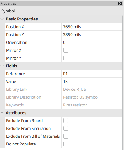
You can also view and edit item properties using the properties manager. The properties manager is a docked panel that displays the properties of the selected item or items for editing. If multiple types of items are selected at once, the properties panel displays only the properties shared by all of the selected item types.
Editing a property in the properties manager immediately applies the change. When multiple items are selected, property modifications are applied to each selected item individually, not to the whole selection as a group. For example, when changing the orientation of multiple items, each item is individually rotated around its own origin, not the group’s origin.
Show the properties manager with View → Show Properties Manager or the ![]() button on the left toolbar.
button on the left toolbar.
In properties dialogs and many other dialogs, any field that contains a numeric value can also accept a basic math expression that results in a numeric value. For example, a dimension may be entered as 2 * 2mm, resulting in a value of 4mm. Basic arithmetic operators as well as parentheses for defining order of operations are supported.
Working with symbols
Placing symbols
To place a symbol in your schematic, use the ![]() button or the A hotkey. The Choose Symbols dialog appears and lets you select a symbol to add. Symbols are grouped by symbol library.
button or the A hotkey. The Choose Symbols dialog appears and lets you select a symbol to add. Symbols are grouped by symbol library.
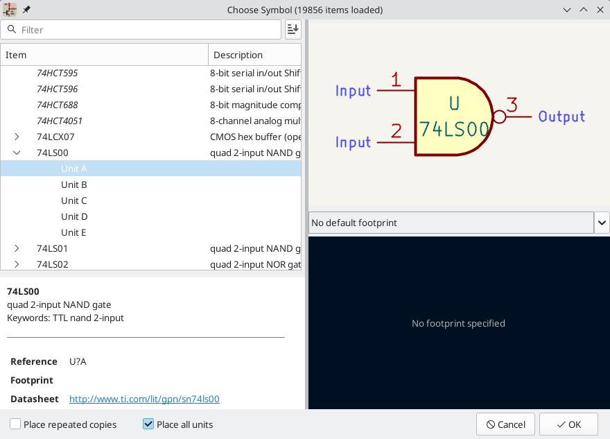
By default, only the symbol/library name and description columns are shown. Additional columns can be added by right-clicking the column header and selecting Select Columns.
The Choose Symbol dialog filters symbols by name, keywords, description, and all additional symbol fields according to what you type into the search field. You can choose to sort search results alphabetically or by best match by clicking on the ![]() button.
button.
Some advanced filters are available:
-
Wildcards:
*matches any number of any characters, including none, and?matches any single character. -
Key-value pairs: if a library part’s description or keywords contain a tag of the format "Key:123", you can match relative to that by typing "Key>123" (greater than), "Key<123" (less than), etc. Numbers may include one of the following case-insensitive suffixes:
p
n
u
m
k
meg
g
t
10-12
10-9
10-6
10-3
103
106
109
1012
ki
mi
gi
ti
210
220
230
240
-
Regular expressions: if you’re familiar with regular expressions, these can be used too. The regular expression flavor used is the wxWidgets Advanced Regular Expression style, which is similar to Perl regular expressions.
If the symbol specifies a default footprint, this footprint will be previewed in the lower right. If the symbol includes footprint filters, alternate footprints that satisfy the footprint filters can be selected in the footprint dropdown menu at right.
After selecting a symbol to place, the symbol will be attached to the cursor. Left clicking the desired location in the schematic places the symbol into the schematic. Before placing the symbol in the schematic, you can rotate it, mirror it, and edit its fields, by either using the hotkeys or the right-click context menu. These actions can also be performed after placement.
If the Place repeated copies option is checked, after placing a symbol KiCad will start placing another copy of the symbol. This process continues until the user presses Esc.
For symbols with multiple units, if the Place all units option is checked, after placing the symbol KiCad will start placing the next unit in the symbol. This continues until the last unit has been placed or the user presses Esc.
Placing power symbols
A power symbol is a symbol representing a connection to a power net. The symbols are grouped in the power library, so they can be placed using the symbol chooser. However, as power placements are frequent, the ![]() tool is available. This tool is similar, except that the search is done directly in the
tool is available. This tool is similar, except that the search is done directly in the power library and any other library that contains power symbols.
Moving symbols
Symbols can be moved using the Move (M) or Drag (G) tools. These tools act on the selected symbol, or if no symbol is selected they act on the symbol under the cursor.
The Move tool moves the symbol itself without maintaining wired connections to the symbol pins.
The Drag tool moves the symbol without breaking wired connections to its pins, and therefore moves the connected wires as well.
You can also Drag symbols by clicking and dragging them with the mouse, depending on the Left button drag gesture setting in the Mouse and Touchpad section of Preferences.
Symbols can also be rotated (R) or mirrored in the X (X) or Y (Y) directions.
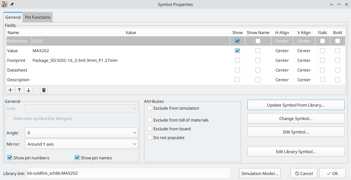
Editing symbol properties
A symbol’s fields can be edited in the symbol’s Properties window. Open the Symbol Properties window for a symbol with the E hotkey or by double-clicking on the symbol.
The Symbol Properties window displays all the fields of a symbol in a table. New fields can be added, and existing fields can be deleted, edited, reordered, moved, or resized. Fields can be arbitrarily named, but names beginning with ki_, e.g. ki_description, are reserved by KiCad and should not be used for user fields.
Each field’s name and value can be visible or hidden, and there are several formatting options: horizontal and vertical alignment, orientation, position, font, text color, text size, and bold/italic emphasis. Field autoplacement can also be enabled on a per-field basis. The displayed position is always indicated for a normally displayed symbol (no rotation or mirroring) and is relative to the anchor point of the symbol.
| Formatting options for symbol fields can be shown or hidden by right-clicking on the header row of the symbol field table and enabling or disabling the desired columns. Not all columns are shown by default. |
The Update Symbol from Library… button is used to update the schematic’s copy of the symbol to match the copy in the library. The Change Symbol… button is used to swap the current symbol to a different symbol in the library. These functions are described later.
Edit Symbol… opens the Symbol Editor to edit the copy of the symbol in the schematic. Note that the original symbol in the library will not be modified. The Edit Library Symbol… button opens the Symbol Editor to edit the original symbol in the library. In this case, the symbol in the schematic will not be modified until the user clicks the Update Symbol from Library… button.
Symbols have several attributes that affect how the symbols are treated by other parts of KiCad.
Exclude from simulation prevents the symbol from being included in SPICE simulations.
Exclude from bill of materials prevents the component from being included in BOM exports.
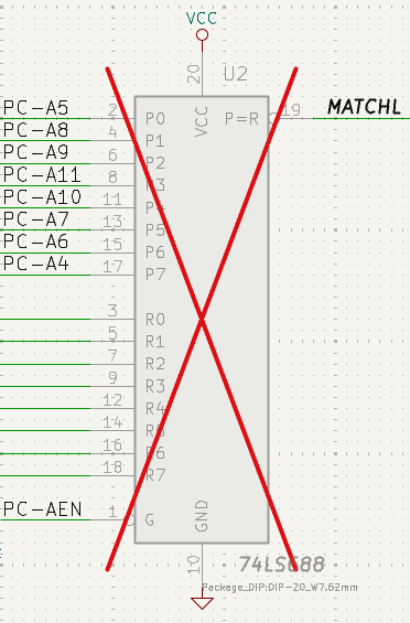
Exclude from board means that the symbol is schematic-only, and a corresponding footprint will not be added to the PCB.
Do not populate means that the component should not be attached to the PCB, although a corresponding footprint should still be added to the board. DNP symbols appear desaturated and with a red "X" over them in the schematic, as shown below.
Editing symbol fields individually
An individual symbol text field can be edited directly with the E hotkey (with a field selected instead of a symbol) or by double-clicking on the field.
Some symbol fields have their own hotkey to edit them directly. With the symbol selected, the Reference, Value, and Footprint fields can be edited with the U, V, or F hotkeys, respectively.
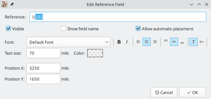
The options in this dialog are the same as those in the full Symbol Properties dialog, but are specific to a single field.
Symbol fields can be automatically moved to an appropriate location with the Autoplace Fields action (select a symbol and press O). Field autoplacement is configurable in the Schematic Editor’s Editing Options, including a setting to always autoplace fields. You can also disable autoplacement for individual fields in the Symbol Properties or Field Properties dialogs.
Updating and exchanging symbols
When a symbol is added to the schematic, KiCad embeds a copy of the library symbol in the schematic so that the schematic is independent of the system libraries. Symbols that have been added to the schematic are not automatically updated when the library changes. Library symbol changes are manually synced to the schematic so that the schematic does not change unexpectedly.
To update symbols in the schematic to match the corresponding symbol, use Tools → Update Symbols from Library, or right click a symbol and select Update Symbol from Library. You can also access the tool from the symbol properties dialog.
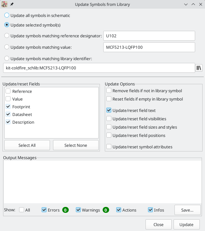
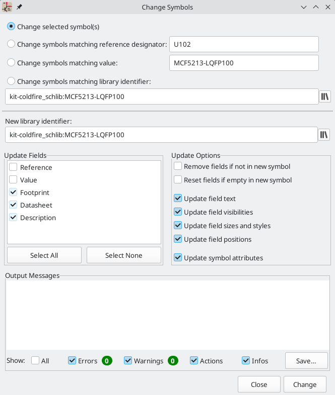
The top of the dialog has options to choose which symbols will be updated. You can update all symbols in the dialog, update only the selected symbols, or update only the symbols that match a specific reference designator, value, or library identifier. The reference designator and value fields support wildcards: * matches any number of any characters, including none, and ? matches any single character.
The middle of the dialog has options to control what parts of the symbol will be updated. You can select specific fields to update or not update, which properties of the fields to update (text, visibility, size and style, and position), and how to handle fields that are missing or empty in the library symbol. You can also choose whether to update symbol attributes, such as do not populate and exclude from simulation / bill of materials / board.
The bottom of the dialog displays messages describing the update actions that have been performed.
To change an existing symbol to a different symbol, use Edit → Change Symbols…, or right click an existing symbol and select Change Symbol…. This dialog is also accessible from the symbol properties dialog.
The options for the Change Symbols dialog are very similar to the Update Symbols from Library dialog.
Another way to swap existing symbols for new ones is to use Tools → Edit Symbol Library Links…. This dialog contains a table of every symbol in the design, grouped by current library symbol. By choosing a new symbol in the New Library Reference column, you can make all instances of the existing symbol instead point to the new symbol. If the Update symbol fields from new library option is used, the contents of the existing symbols' fields will be updated to match the new symbols' fields.
The Map Orphans button attempts to automatically remap orphaned symbols to symbols with the same name in an active library. For example, if there is a symbol with the current library reference mylib:symbol123, but the mylib library cannot be found, the Map Orphans button will attempt to find a symbol named symbol123 in any of the libraries that are present. This button is only enabled if orphaned symbols are present in the schematic (see the legacy schematics section).
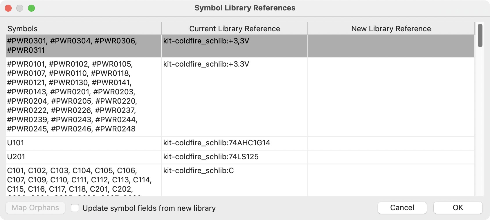
This dialog is primarily useful for managing symbols that appear in multiple libraries, when you want to switch from one library to another. For example, if a schematic uses symbols that are in both a global library and a project-specific library, the Symbol Library References dialog could be used to switch between using the global symbols or the equivalent project-specific symbols. It does not have features for fine-grained control of how fields are updated; for that, use the Change Symbols dialog.
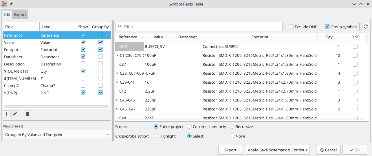
Symbol Fields Table
The Symbol Fields Table allows you to view and modify field values for all symbols in a spreadsheet interface. You can open the Symbol Fields Table with the ![]() button.
button.
Cells are navigated with the arrow keys, or with Tab / Shift+Tab to move right / left and Enter to move down, respectively.
A range of cells can be selected by clicking and dragging. The whole range of selected cells will be copied (Ctrl+C) or pasted into (Ctrl+V) on a copy or paste action. Copying a range of cells from the table can be useful for creating a BOM. More details of copying and pasting cells are described below.
Any symbol field can be shown or hidden using the Show checkboxes on the left or by right-clicking on the header of the table. New symbol fields can be added using the ![]() button; a field with that name will be added to every symbol. Each field can have its own label, which doesn’t have to be the same as the field name, and is used as the column header. Fields can be renamed with the
button; a field with that name will be added to every symbol. Each field can have its own label, which doesn’t have to be the same as the field name, and is used as the column header. Fields can be renamed with the ![]() button or deleted with the
button or deleted with the ![]() button.
button.
Several virtual fields are available in this dialog that do not directly represent symbol fields. Adding a field with one of the following names will not create a new field in the symbols, but will create a special column in the table with auto-generated values for each symbol:
-
${QUANTITY}creates a field that contains the number of grouped instances of that symbol. -
${ITEM_NUMBER}creates a field that contains the row number of the symbol in the table. -
${DNP}creates a field with a checkbox that controls the symbol’s DNP attribute. In the BOM, this field resolves to the string "DNP" if the symbol’s DNP attribute is set, or an empty string otherwise. -
${EXCLUDE_FROM_BOARD}creates a field with a checkbox that controls the symbol’s exclude from board attribute. In the BOM, this field resolves to the string "Excluded from board" if the symbol’s exclude from board attribute is set, or an empty string otherwise. -
${EXCLUDE_FROM_SIM}creates a field with a checkbox that controls the symbol’s exclude from simulation attribute. In the BOM, this field resolves to the string "Excluded from simulation" if the symbol’s exclude from simulation attribute is set, or an empty string otherwise. -
${EXCLUDE_FROM_BOM}creates a field with a checkbox that controls the symbol’s exclude from BOM attribute. Symbol with the exclude from BOM attribute set are not included in the BOM.
Similar symbols can optionally be grouped by any symbol field using the Group By checkboxes. Symbols are grouped into a single row in the table if all of their Group By fields are identical. The grouped row can be expanded to show the individual symbols by clicking the arrow at the left of the row. The Group Symbols checkbox enables or disables symbol grouping, and the ![]() button recalculates groupings.
button recalculates groupings.
Presets are available to configure the list of fields. Presets store which fields are displayed, which fields are used for grouping, and the column order. You can create and save your own presets or use one of several default presets. Custom presets can be deleted in this dialog or in the Schematic Setup dialog.
Symbols can be filtered by reference designator using the Filter textbox at the top. The filter supports wildcards: * matches any number of any characters, including none, and ? matches any single character. You can also change the display scope, showing only symbols in the current sheet, the current sheet and all of its subsheets, or the entire project. Symbols with the DNP (do not populate) attribute set can be optionally excluded by checking the Exclude DNP box.
You can cross-probe from this dialog by selecting a row in the table. Depending on the Cross-probe action setting at the bottom of the dialog, this can highlight the corresponding symbol in the schematic, select the corresponding symbol in the schematic, or do nothing. The selection action can also select the symbol’s footprint in the board editor, depending on the PCB Editor cross-probing settings.
The Symbol Fields Table is also a bill of materials tool. You can use the Export button to save the symbol fields to an external file. The fields are exported to the BOM exactly as they are currently shown in the spreadsheet view. File format settings are configured in the Export tab. For more information about exporting a BOM, see the BOM tool documentation.
Tricks to simplify filling fields
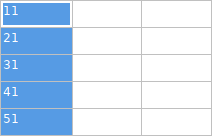
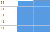
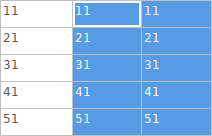
There are several special copy/paste methods in the spreadsheet for pasting values into larger regions, including auto-incrementing pasted cells. These features may be useful when pasting values that are shared in several symbols.
These methods are illustrated below.
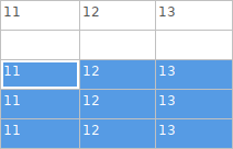
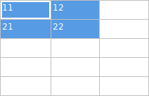
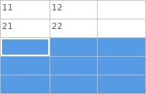
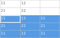
| 1. Copy (Ctrl+C) | 2. Select target cells | 3. Paste (Ctrl+V) |
|---|---|---|
|
|
|
|
|
|
|
|
|
|
|
|
|
|
|
| These techniques are also available in other dialogs with a grid control element. |
Reference Designators and Symbol Annotation
Reference designators are unique identifiers for components in a design. They are often printed on a PCB and in assembly diagrams, and allow you to match symbols in a schematic to the corresponding components on a board.
In KiCad, reference designators consist of a letter indicating the type of component (R for resistor, C for capacitor, U for IC, etc.) followed by a number. If the symbol has multiple units then the reference designator will also have a trailing letter indicating the unit. Symbols that don’t have a reference designator set have a ? character instead of the number. Reference designators must be unique.
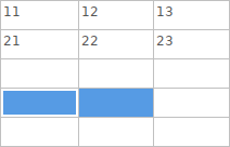
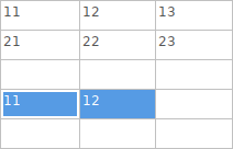
Reference designators can be automatically set when symbols are added to the schematic, and you can set or reset reference designators yourself by manually editing an individual symbol’s reference designator field or in bulk using the Annotation tool.
| The process of setting a symbol’s reference designator is called annotation. |
Auto-annotation
When auto-annotation is enabled, symbols will be automatically annotated when they are added to the schematic. You can enable auto-annotation by checking the Automatically annotate symbols checkbox in the Schematic Editor → Annotation Options pane in Preferences. Auto-annotation can also be toggled using the ![]() button in the left toolbar.
button in the left toolbar.
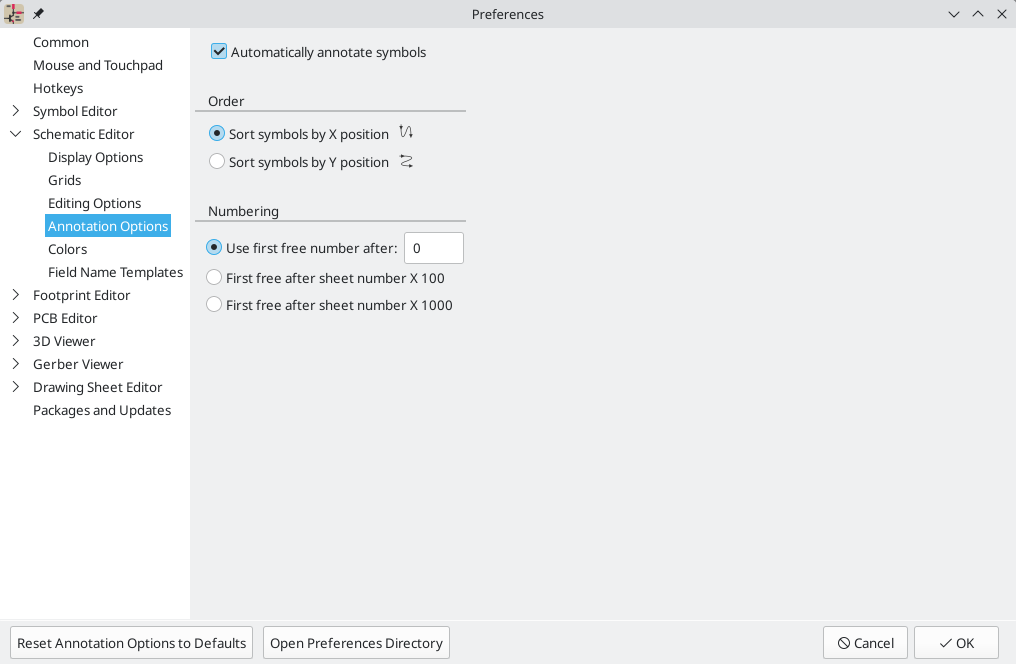
When multiple symbols are added simultaneously, they are annotated according to the Order setting, sorted by either X or Y position.
The Numbering option sets the starting number for new reference designators. This can be the lowest available number, or a number based on the sheet number.
For more information about annotation options, see the documentation for the Annotation tool.
Herramienta de Anotado
The Annotation tool automatically assigns reference designators to symbols in the schematic. To launch the Annotation tool, click the ![]() button in the top toolbar.
button in the top toolbar.
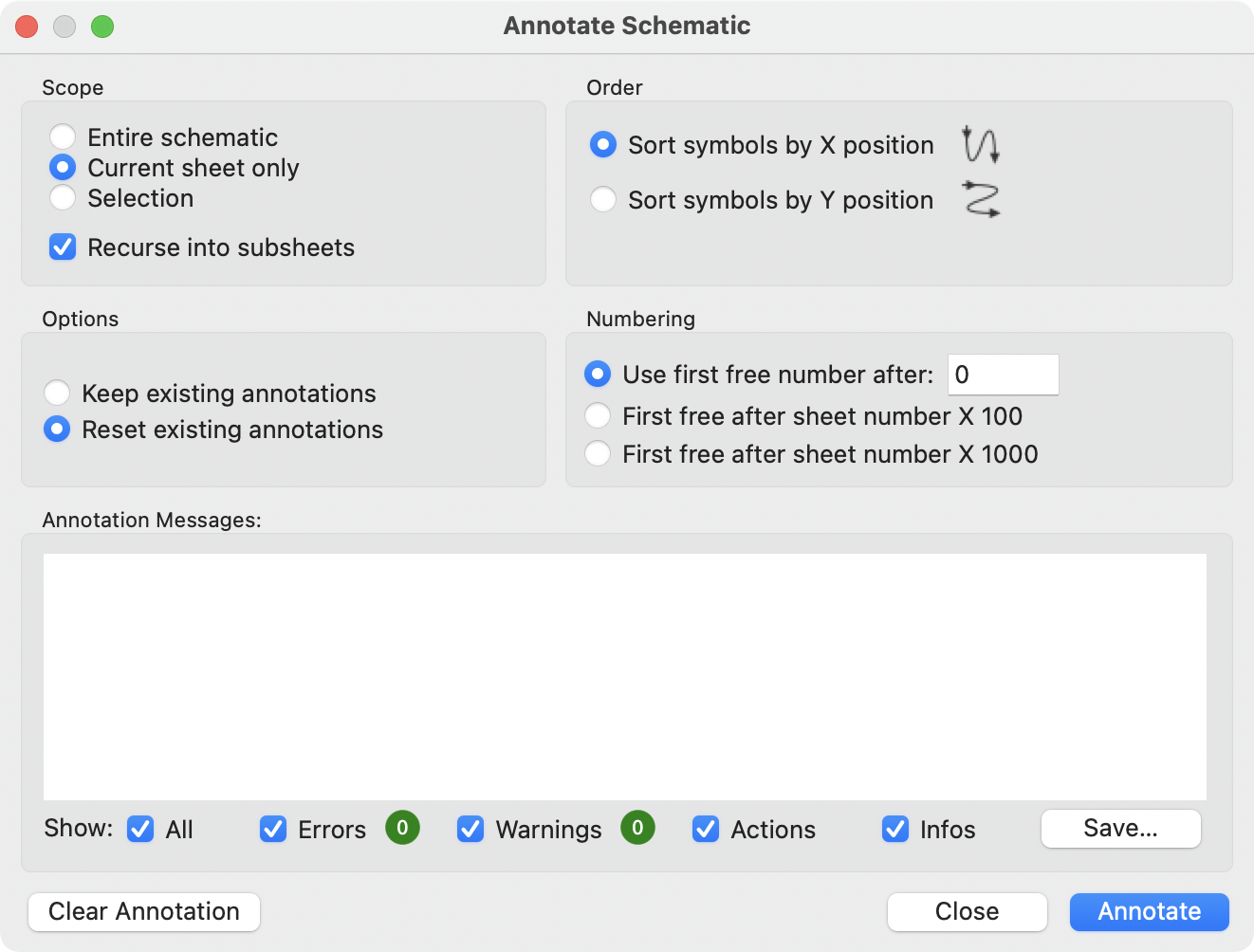
The tool provides several options to control how symbols are annotated.
Scope: Selects whether annotation is applied to the entire schematic, to only the current sheet, or to only the selected symbols. If the Recurse into subsheets option is selected, symbols in subsheets of the selected scope will be reannotated; otherwise symbols in subsheets will not be reannotated. For example, if Recurse into subsheets and Selection only selected, symbols in any selected subsheets will be reannotated.
Options: Selects whether annotation should apply to all symbols and reset *existing reference designators, or apply only to unannotated symbols.
Order: Chooses the direction of numbering. If symbols are sorted by X position, all symbols on the left side of a schematic sheet will be lower numbered than symbols on the right side of the sheet. If symbols are sorted by Y position, all symbols on the top of a sheet will be lower numbered than symbols at the bottom of the sheet.
Numbering: Selects the starting point for numbering reference designators. The lowest unused number above the starting point is picked for each reference designator. The starting point can be an arbitrary number (typically zero), or it can be the sheet number multiplied by 100 or 1000 so that each part’s reference designator corresponds to the schematic page it is on.
The Clear Annotation button clears all reference designators in the selected scope.
Annotation messages can be filtered with the checkboxes at the bottom or saved to a report using the Save… button.
Electrical Connections
There are two primary ways to establish connections: wires and labels. Wires make direct connections, while labels connect to other labels with the same name. Both wires and labels are shown in the schematic below.
Connections can also be made with buses and with implicit connections via hidden power pins.
This section will also discuss two special types of symbols that can be added with the "Power symbol" button on the right toolbar:
-
Power symbols: symbols for connecting wires to a power or ground net.
-
PWR_FLAG: a specific symbol for indicating that a net is powered when it is not connected to a power output pin (for example, a power net that is supplied by an off-board connector).
Wires
Wires are used to directly establish electrical connections between two points. To establish a connection, a segment of wire must be connected by its end to another segment or to a pin. Only wire ends create connections; if a wire crosses the middle of another wire, a connection will not be made.
Unconnected wire ends have a small square that indicates the connection point. The square disappears when a connection is made to the wire end. Unconnected pins have a circle, which also disappears when a connection is made.
| Wires connect with other wires or pins only if their ends coincide exactly. Therefore it is important to keep symbol pins and wires aligned to the grid. It is recommended to always use a 50 mil grid when placing symbols and drawing wires because the KiCad standard symbol library and all libraries that follow its style also use a 50 mil grid. |
| Symbols, wires, and other elements that are not aligned to the grid can be snapped back to the grid by selecting them, right clicking, and selecting Align Elements to Grid. |
Drawing and editing wires
To begin connecting elements with wire, use the Wire tool ![]() in the right toolbar (w). Wires can also be automatically started by clicking on an unconnected symbol pin or wire end.
in the right toolbar (w). Wires can also be automatically started by clicking on an unconnected symbol pin or wire end.
You can restrict wires to 90 degree angles using the ![]() button in the left toolbar, or to 45 degree angles with the
button in the left toolbar, or to 45 degree angles with the ![]() button. The
button. The ![]() button allows you to place wires at any angle. You can cycle through these modes using Shift+Space, or select the desired mode in Preferences → Schematic Editor → Editing Options. These modes affect graphic lines in addition to wires.
button allows you to place wires at any angle. You can cycle through these modes using Shift+Space, or select the desired mode in Preferences → Schematic Editor → Editing Options. These modes affect graphic lines in addition to wires.
As in the PCB editor, the / hotkey switches wire posture.
Wires can be moved and edited using the Move (M) or Drag (G) tools. As with symbols, the Move tool moves only the selected segment, without maintaining existing connections to other segments. The Drag tool maintains existing connections.
You can select connected wires using the Select Connection tool (Alt+4). This tool selects all connected wire segments until it reaches a junction, starting with the selected segment or the segment under the cursor. Using the tool again expands the existing selection to the next junction.
You can break a wire segment into two pieces by right-clicking a wire and selecting Slice. The segment will be separated at the current mouse position. You can also separate a wire segment from the adjacent segments by right-clicking the segment and selecting Break.
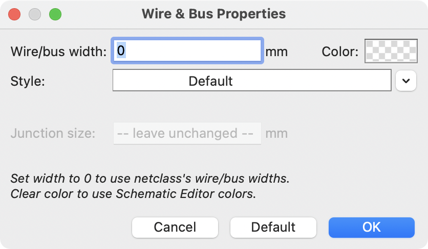
Normally the line style of a wire follows the net’s netclass settings (nets are in the Default netclass if no other netclass is specified). However, the line style for the selected wire segments can be overridden in the wire’s properties dialog (E when a wire segment is selected). The wire’s width, color, and line style (solid, dashed, dotted, etc.) can be set. Setting the width to 0, clearing the color, and using the Default line style uses the default width, color, and style, respectively, from the netclass settings. If a wire junction is included in the selection, the junction size can also be edited here.
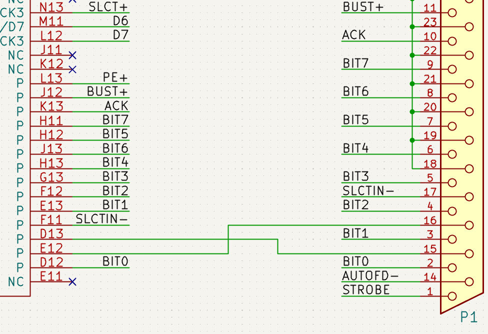
Wire Junctions
Wires that cross are not implicitly connected. It is necessary to join them by explicitly adding a junction dot if a connection is desired (![]() button in the right toolbar). Junction dots will be automatically added to wires that start or end on top of an existing wire.
button in the right toolbar). Junction dots will be automatically added to wires that start or end on top of an existing wire.
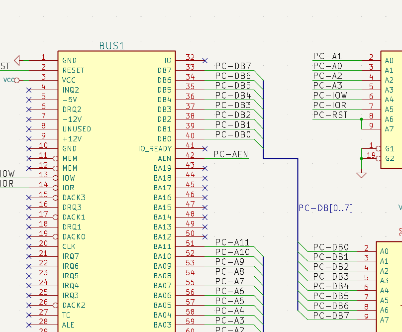
Junction dots are used in the schematic figure above on the wires connected to P1 pins 18, 19, 20, 21, 22, and 23.
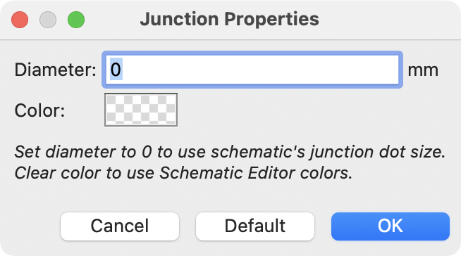
Junction size automatically follows the schematic’s Junction dot size setting in Schematic Setup → General → Formatting. Color follows the netclass setting. The automatic size and color can be overridden in each junction dot’s properties; a size of 0 is equivalent to the schematic default size, and clearing the color uses the netclass color.
Labels
Labels are used to assign net names to wires and pins. Wires with the same net name are considered to be connected, so labels can be used to make connections without drawing direct wire connections.
A net can only have one name. If two different labels are placed on the same net, an ERC violation will be generated. Only one of the net names will be used in the netlist. The final net name is determined according to the rules described below.
There are three types of labels, each with a different connection scope.
-
Local labels, also referred to simply as labels, only make connections within a sheet. Add a local label with the
 button in the right
toolbar.
button in the right
toolbar. -
Global labels make connections anywhere in a schematic, regardless of sheet. Add a global label with the
 button in the right
toolbar.
button in the right
toolbar. -
Hierarchical labels connect to hierarchical sheet pins and are used in hierarchical schematics for connecting child sheets to their parent sheet. Add a hierarchical label with the
 button in the right toolbar.
| Labels that have the same name will connect, regardless of the label type, if they are in the same sheet. |
Adding and editing labels
After using the appropriate button or hotkey to create a label, the Label Properties dialog appears.
The Label field sets the label’s text, which determines the net that the label assigns to its attached wire. Label text supports markup for overbars, subscripts, etc., as well as variable substitution. Use the Syntax help link in the dialog for a summary.
There are several options to control the label’s appearance. You can change the font, size, and color of the text, and set bold and italic emphasis. You can also set the orientation of the text relative to the label’s connection point. Hierarchical and global labels have several additional options: the Auto option automatically sets the label orientation based on the connected schematic elements, and Shape option controls the shape of the label outline (Input, Output, Bidirectional, Tri-state, or Passive). The outline shape is purely visual and has no electrical consequence.
| The default text size can be set for a schematic in Schematic Setup, and the default font can be set in Preferences. |
| Global labels have additional settings to control margins around the label text in the Schematic Setup dialog. |
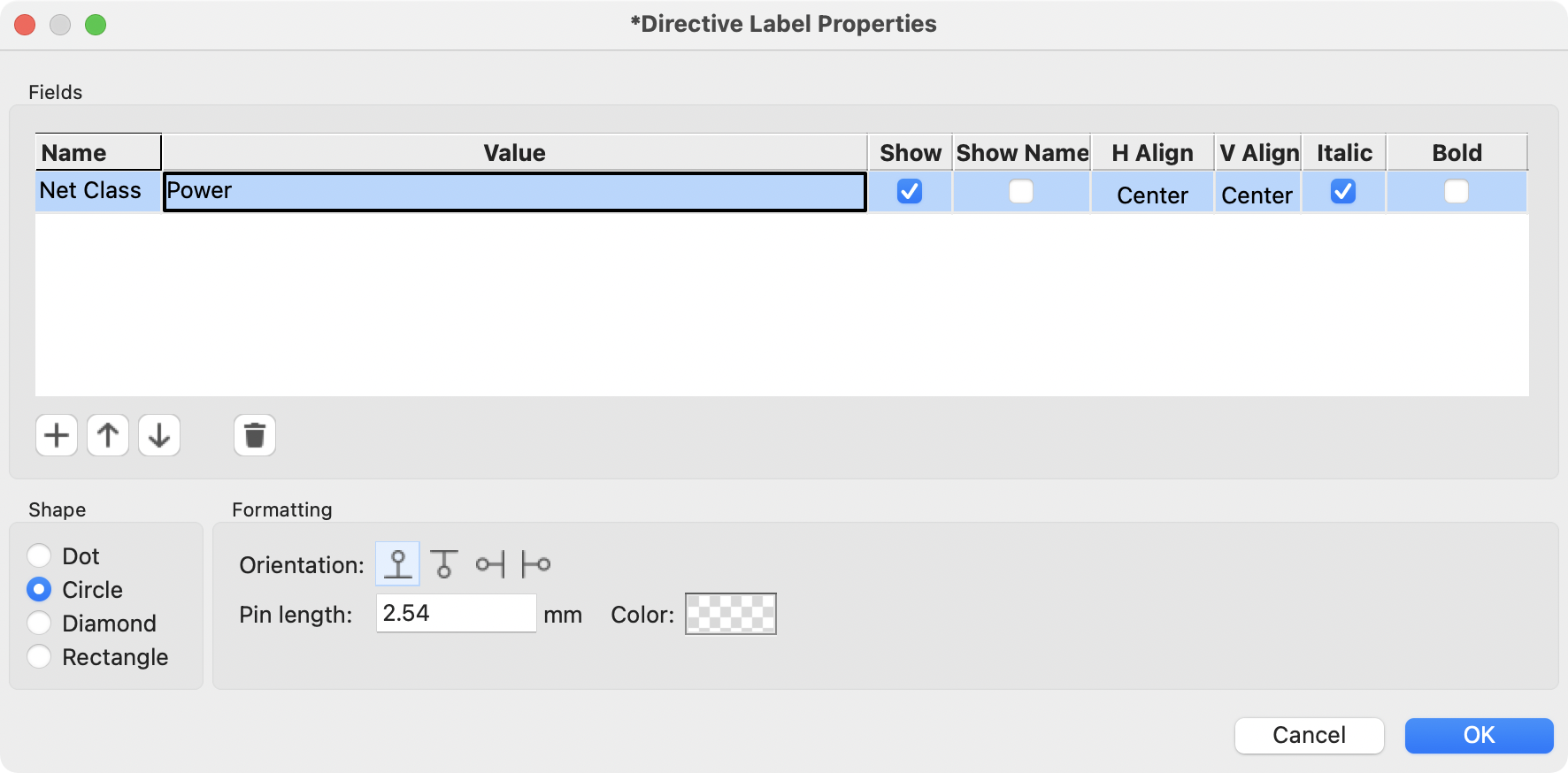
Labels can also have fields added to them. Two fields have special meaning (Net Class and Sheet References, described below), but arbitrary fields can also be added. Label fields behave like symbol fields: you can show or hide their name and value and adjust the alignment, orientation, position, size, font, color, and emphasis.
| Formatting options for label fields can be shown or hidden by right-clicking on the header row of the label field table and enabling or disabling the desired columns. Not all columns are shown by default. |
Like symbol fields, label fields can be edited individually by opening the properties of a specific label field from the schematic (double click the label field, or use E).
After accepting the label properties, the label is attached to the cursor for placement. The connection point for a label is the small square in the corner of the label. The square disappears when the label is connected to a wire or the end of a pin.

The connection point’s position relative to the label text can be changed by choosing a different label orientation in the label’s properties, or by mirroring/rotating the label.
The Label Properties dialog can be accessed at any time by selecting a label and using the E hotkey, double-clicking on the label, or with Properties… in the right-click context menu.
Assigning net classes with labels
In addition to assigning net names, labels can be used to assign net classes. A label field named Net Class assigns the specified netclass to the net associated with the label. To make it easier to assign net classes in this way, Net Class is the default name for new label fields, and Net Class fields present a dropdown list of all the net classes in the design. Net classes must be created in the Schematic Setup or Board Setup windows before they can be assigned with a label field.
For more information about assigning netclasses, see the netclass documentation.
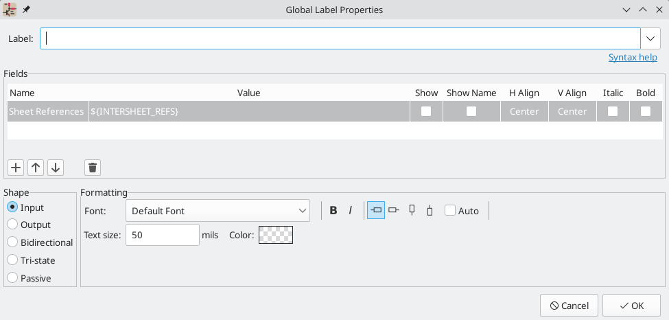
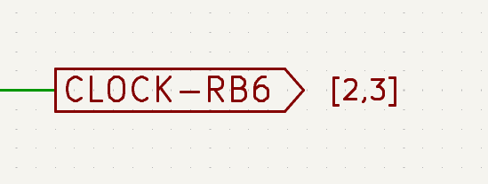
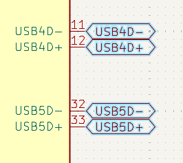
Inter-sheet references
Global labels can display inter-sheet references, which are a list of page numbers for other places in the schematic where the same global label appears. Clicking an inter-sheet reference travels to the listed page. If multiple references are listed, clicking the reference list brings up a menu to select the desired page.
Inter-sheet references are globally controlled in the Schematic Setup window’s Formatting page. References can be enabled or disabled, and the displayed format for the list can be adjusted, including with optional prefix or suffix characters.
The image below shows a global label with inter-sheet references to two other schematic pages. A prefix and suffix of [ and ], respectively, were added in Schematic Setup.
A Sheet References field with value ${INTERSHEET_REFS} is automatically added to global labels, and is used to control the appearance of inter-sheet references for that label. The ${INTERSHEET_REFS} text variable gets expanded to the full list of inter-sheet references for the global label, as configured in Schematic Setup. Visibility of inter-sheet references is globally controlled in Schematic Setup rather than with the Sheet References field visibility control. The Sheet References field has no meaning for other types of labels.
Buses
Buses are a way to group related signals in the schematic in order to simplify complicated designs. Buses can be drawn like wires using the bus tool ![]() , and are named using labels the same way signal wires are.
, and are named using labels the same way signal wires are.
In the following schematic, many pins are connected to buses, which are the thick blue lines in the center.
Miembros del Bus
There are two types of bus in KiCad 6.0 and later: vector buses and group buses.
A vector bus is a collection of signals that start with a common prefix and end with a number. Vector buses are named <PREFIX>[M..N] where PREFIX is any valid signal name, M is the first suffix number, and N is the last suffix number. For example, the bus DATA[0..7] contains the signals DATA0, DATA1, and so on up to DATA7. It doesn’t matter which order M and N are specified in, but both must be non-negative.
A group bus is a collection of one or more signals and/or vector buses. Group buses can be used to bundle together related signals even when they have different names. Group buses use a special label syntax:
<OPTIONAL_NAME>{SIGNAL1 SIGNAL2 SIGNAL3}
The members of the group are listed inside curly braces ({}) separated by space characters. An optional name for the group goes before the opening curly brace. If the group bus is unnamed, the resulting nets on the PCB will just be the signal names inside the group. If the group bus has a name, the resulting nets will have the name as a prefix, with a period (.) separating the prefix from the signal name.
For example, the bus {SCL SDA} has two signal members, and in the netlist these signals will be SCL and SDA. The bus USB1{DP DM} will generate nets called USB1.DP and USB1.DM. For designs with larger buses that are repeated across several similar circuits, using this technique can save time.
Group buses can also contain vector buses. For example, the bus MEMORY{A[7..0] D[7..0] OE WE} contains both vector buses and plain signals, and will result in nets such as MEMORY.A7 and MEMORY.OE on the PCB.
Bus wires can be drawn and connected in the same manner as signal wires, including using junctions to create connections between crossing wires. Like signals, buses cannot have more than one name — if two conflicting labels are attached to the same bus, an ERC violation will be generated.
Conexión entre miembros de bus
Pins connected between the same members of a bus must be connected by labels. It is not possible to connect a pin directly to a bus; this type of connection will be ignored by KiCad.
En el ejemplo anterior, las conexiones son realizas por las etiquetas colocadas sobre los hilos conectados a los pines. Las entradas de bus (segmentos de hilo a 45 grados) son solo representaciones gráficas, y no forman necesariamente conexiones lógicas.
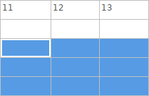
In fact, using the repetition command (Insert), connections can be very quickly made in the following way, if component pins are aligned in increasing order (a common case in practice on components such as memories, microprocessors…):
-
Place the first label (for example
PCA0) -
Use the repetition command as much as needed to place members. KiCad will automatically create the next labels (
PCA1,PCA2…) vertically aligned, theoretically on the position of the other pins. -
Dibuje el hilo bajo la primera etiqueta. Después utilice el comando repetir para colocar los otros hilos bajo el resto de etiquetas.
-
Si fuera necesario, coloque las entradas al bus del mismo modo (coloque la primera entrada y utilice el comando repetir)
|
In the Schematic Editor → Editing Options section of the Preferences menu, you can set the repetition parameters:
|
Bus unfolding
The unfold tool allows you to quickly break out signals from a bus. To unfold a signal, right-click on a bus object (a bus wire, etc) and choose Unfold from Bus. Alternatively, use the Unfold Bus hotkey (default: C) when the cursor is over a bus object. The menu allows you to select which bus member to unfold.
After selecting the bus member, the next click will place the bus member label at the desired location. The tool automatically generates a bus entry and wire leading up to the label location. After placing the label, you can continue placing additional wire segments (for example, to connect to a component pin) and complete the wire in any of the normal ways.
Bus aliases
Bus aliases are shortcuts that allow you to work with large group buses more efficiently. They allow you to define a group bus and give it a short name that can then be used instead of the full group name across the schematic.
To create bus aliases, open the Bus Alias Definitions pane in Schematic Setup.
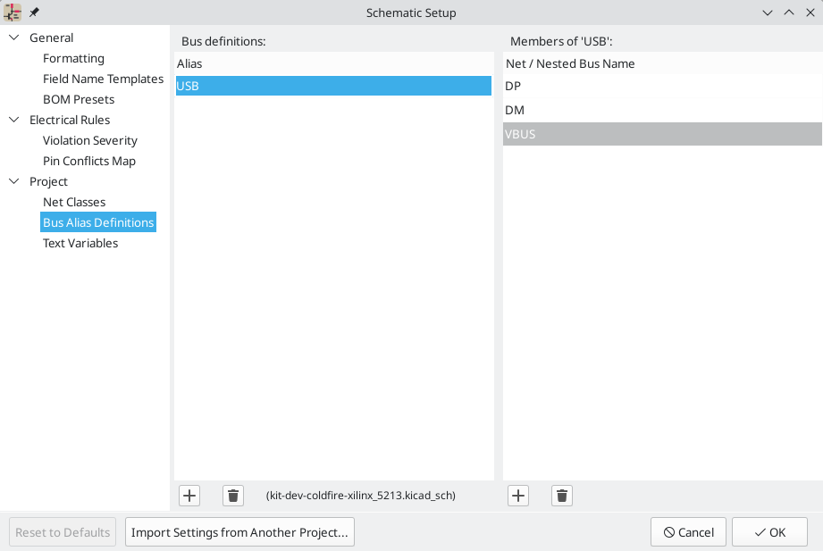
An alias may be named any valid signal name. Using the dialog, you can add signals or vector buses to the alias. As a shortcut, you can type or paste in a list of signals and/or buses separated by spaces, and they will all be added to the alias definition. In this example, we define an alias called USB with members DP, DM, and VBUS.
After defining an alias, it can be used in a group bus label by putting the alias name inside the curly braces of the group bus: {USB}. This has the same effect as labeling the bus {DP DM VBUS}. You can also add a prefix name to the group, such as USB1{USB}, which results in nets such as USB1.DP. For complicated buses, using aliases can make the labels on your schematic much shorter. Keep in mind that the aliases are just a shortcut, and the name of the alias is not included in the netlist.
Bus aliases are saved in the schematic file that is opened when the alias is created. The Bus Alias Definitions window shows the schematic file associated with the selected alias at the bottom of the alias list. Any aliases created in a given schematic sheet are available to use in any other schematic sheet that is in the same hierarchical design. If multiple sheets in a hierarchical design contain identically-named bus aliases, the aliases must all have the same members. ERC will report a violation if multiple bus aliases with the same name do not have consistent members.
Buses with more than one label
KiCad 5.0 and earlier allowed the connection of bus wires with different labels together, and would join the members of these buses during netlisting. This behavior has been removed in KiCad 6.0 because it is incompatible with group buses, and also leads to confusing netlists because the name that a given signal will receive is not easily predicted.
If you open a design that made use of this feature in a modern version of KiCad, you will see the Migrate Buses dialog which guides you through updating the schematic so that only one label exists on any given set of bus wires.
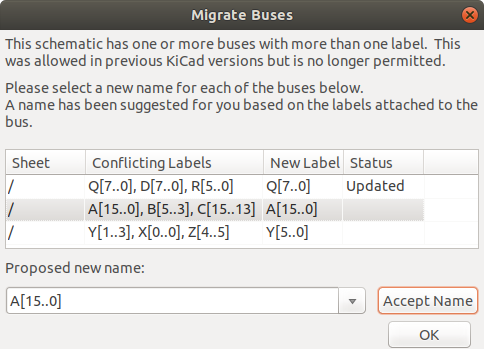
For each set of bus wires that has more than one label, you must choose the label to keep. The drop-down name box lets you choose between the labels that exist in the design, or you can choose a different name by manually entering it into the new name field.
Símbolos de Potencia
Power symbols are symbols that are conventionally used to represent a connection to a power net, such as VCC or GND. Power symbols are virtual: they do not represent a physical component on the PCB.
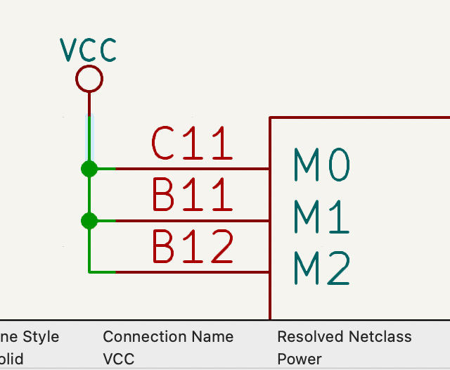
In addition to being a visual indicator that the attached net is a power rail, power symbols make global connections: two power symbols with the Value connect to each other anywhere in the schematic, regardless of sheet. The power symbol’s Value field determines the name of the attached net.
| In previous versions of KiCad, power symbols used invisible power input pins, which make implicit global connections based on the pin name as described below. Beginning in KiCad 8, power symbols do not need to use invisible pins, and the global connection is made based on the power symbol’s value. |
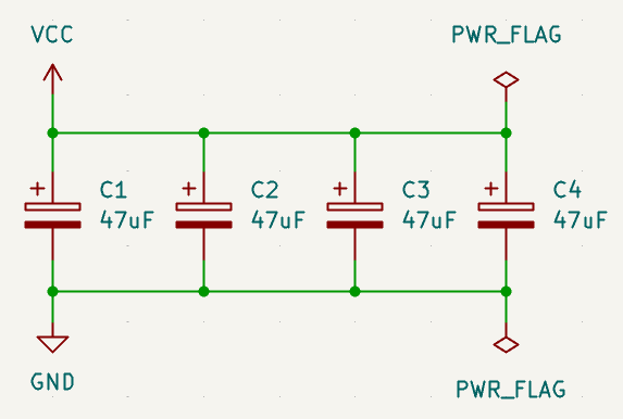
In the figure below, power symbols are used to connect the positive and negative terminals of the capacitors to the VCC and GND nets, respectively.
In the KiCad standard library, power symbols are found in the power library, but power symbols can be created in any library. Creating custom power symbols is described in the symbol editor documentation. Instead of making a new symbol, you can also modify an existing power symbol in the schematic: changing its Value field will change the net the power symbol connects to.
Net name assignment rules
Every net in the schematic is assigned a name, whether that name is specified by the user or automatically generated by KiCad.
When multiple labels are attached to the same net, the final net name is determined in the following order, from highest priority to lowest:
-
Etiquetas globales
-
Local labels
-
Etiquetas de Jerarquia
-
Hierarchical sheet pins
If there are multiple labels of one type attached to a net, the names are sorted alphabetically and the first is used.
If a net travels through multiple sheets of a hierarchy, it will take its name from the highest level of the hierarchy where it has a hierarchical label or local label. As usual, local labels take priority over hierarchical labels.
If none of the label types above are attached to a net, the net’s name is automatically generated based on the connected symbol pins.
PWR_FLAG
Two PWR_FLAG symbols are visible in the screenshot above. They indicate to ERC that the two power nets VCC and GND are actually connected to a power source, as there is no explicit power source such as a voltage regulator output attached to either net.
Without these two flags, the ERC tool would diagnose: Error: Input Power pin not driven by any Output Power pins.
The PWR_FLAG symbol is found in the power symbol library. The same effect can be achieved by connecting any power output pin to the net.
No-connection flag
No-connection flags (![]() ) are used to indicate that a pin is intentionally unconnected. These flags prevent "unconnected pin" ERC warnings for pins that are intentionally unconnected. Also, while symbol pins that are stacked on top of each other are normally connected to the same net, if a no-connection flag is added to the stacked pins they will instead be connected to separate nets.
) are used to indicate that a pin is intentionally unconnected. These flags prevent "unconnected pin" ERC warnings for pins that are intentionally unconnected. Also, while symbol pins that are stacked on top of each other are normally connected to the same net, if a no-connection flag is added to the stacked pins they will instead be connected to separate nets.
Note that no-connection flags are distinct from the "unconnected" symbol pin type, although they both prevent "unconnected pin" ERC warnings on the pin in question and prevent stacked pins from connecting to each other.
Hidden Power Pins
When the power pins of a symbol are visible, they must be connected, as with any other signal. However, symbols are sometimes drawn with hidden power input pins, which are connected implicitly. KiCad automatically connects invisible pins with type Power Input to a global net with the same name as the pin. For example, if a symbol has a hidden power input pin named VCC, this pin will be globally connected to the VCC net on all sheets. This kind of implicit connection is not recommended in new designs.
| Care must be taken with hidden power input pins because they can create unintentional connections. By nature, hidden pins are invisible and do not display their pin name. This makes it easy to accidentally connect two power pins to the same net. For this reason, using invisible power pins in symbols is not recommended and is only supported for compatibility with legacy designs and symbols. |
|
Hidden pins can be shown in the schematic by checking the Show hidden
pins option in the Schematic Editor → Display Options section
of the preferences, or by selecting View → Show hidden pins.
There is also a toggle icon |
Netclasses
Netclasses are groups of nets that can be assigned design rules (for the PCB) and graphical properties (for the schematic). In KiCad, each net is part of exactly one net class. If you do not add a net to a specific class, it will be part of the Default class, which always exists.
Net classes may be created and edited in either the Schematic or Board Setup dialogs. Nets can be added to netclasses in either the schematic or board using pattern-based assignments described below. Nets can also be assigned to netclasses in the schematic using graphical assignments with net class directives or net labels.
Selecting a wire or label displays the net’s netclass in the message panel at the bottom of the window.
Managing netclasses in Schematic Setup
Netclasses are managed in the Net Classes panel of the Schematic Setup dialog.
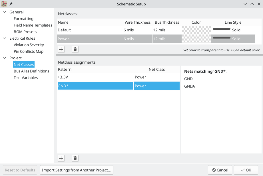
The top pane lists the netclasses that exist in the design. The Default netclass always exists, and you can add additional netclasses with the ![]() button or remove the selected netclass with the
button or remove the selected netclass with the ![]() button.
button.
Each netclass can have unique graphic properties that determine how wires of that netclass are displayed in the schematic. Wire and bus thicknesses, color, and line style (solid, dashed, dotted, etc.) can all be adjusted. Setting the color to transparent will use the theme’s default wire/bus color for the netclass, which is configurable in Preferences.
You can also set board design rules for each netclass, although the DRC fields are hidden by default. Right click the header row to show or hide additional columns. For more information about setting netclass design rules, see the PCB editor documentation.
The bottom pane lists pattern-based netclass assignments. Each row has a net name pattern and a netclass; nets with names that match the pattern are assigned to the specified netclass. If a net matches multiple patterns, the first match is used. Pattern-based netclass assignments are dynamic: when a new net is added that matches an existing pattern, it will be assigned to the associated netclass automatically. Net patterns can use both wildcards (* to match any number of any characters, including none, and ? to match any character) and regular expressions. The nets that match the selected pattern are displayed to the right of the pattern list.
For example, the net* pattern matches nets named net, net1, network, and any other net name beginning with net. Because * has a slightly different meaning in a regular expression (* matches zero or more of the preceding character), the net* pattern would also match a net named ne.
Remember that net names must include the full sheet path. For example, a
locally labeled net in the root sheet has a name prefixed with /.
|
Use the ![]() button to add a net class assignment pattern or the
button to add a net class assignment pattern or the ![]() button to remove a pattern.
button to remove a pattern.
A netclass pattern containing only the * wildcard will match all
explicitly named nets, but will not match unlabeled nets. To match
unlabeled nets, you can include more of the net name before the wildcard
character. All unlabeled nets have names that begin with Net-, so the
pattern Net-* will match all unlabeled nets. You can also assign a
netclass to an unlabeled net using a
net class directive.
|
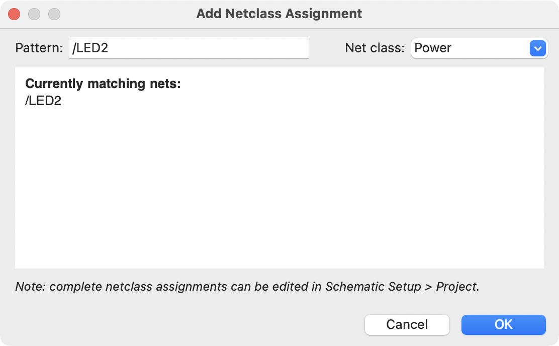
Instead of adding netclass patterns in the Schematic Setup dialog, you can directly create netclass patterns from the schematic canvas. Right click a net and select Assign Netclass… to bring up the Add Netclass Assignment dialog. The netclass pattern is pre-filled with the name of the selected net, but the pattern can be changed if desired. All nets matching the pattern are displayed in the dialog. This method can only be used on nets with an assigned name.
Graphically assigning netclasses in the schematic
As an alternative to pattern-based netclass assignment, netclasses can be graphically assigned to nets in the schematic using either net class directives or labels. Netclasses must be created in Schematic Setup before they can be assigned graphically.
In the image below, a net class directive is used to assign signals to the 50R netclass.
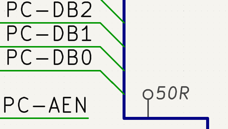
Net class directives are added with the ![]() button in the right toolbar. They behave like labels, except that they cannot be used to name a net. The attached net is assigned a netclass according to the value of the directive’s
button in the right toolbar. They behave like labels, except that they cannot be used to name a net. The attached net is assigned a netclass according to the value of the directive’s Net Class field. The Net Class field presents a dropdown list of all the net classes in the design.
If a directive is attached to a bus, all members of the bus are assigned to the specified net class.
In addition to the associated netclass, you can edit the directive’s shape (dot, circle, diamond, or rectangle), orientation, pin length, and color in the directive’s properties.
Net labels can also be used to assign netclasses to nets by adding a Net Class field to the label.
If more than one different netclass is graphically assigned to a single net, ERC will report an issue. Graphical netclass assignments override pattern-based assignments: if a net matches a netclass pattern assignment and also has a netclass assigned graphically, the graphically assigned netclass will be used.
You can show or hide netclass directives in the schematic using the View → Show Netclass Directives option.
Graphical items
Text, graphic shapes, and images can be added to schematics for documentation purposes. These items do not have any electrical effect on the schematic.
The image below shows graphic lines and text ("COMMUNICATION DSP") in addition to symbols and several types of labels.
Text and text boxes
Two kinds of text can be added to schematics, which are referred to as text (![]() ) and text boxes (
) and text boxes (![]() ). Both are added using their respective buttons in the right toolbar. Text boxes are similar to regular text except that they have an optional border and they automatically reflow text within that border.
). Both are added using their respective buttons in the right toolbar. Text boxes are similar to regular text except that they have an optional border and they automatically reflow text within that border.
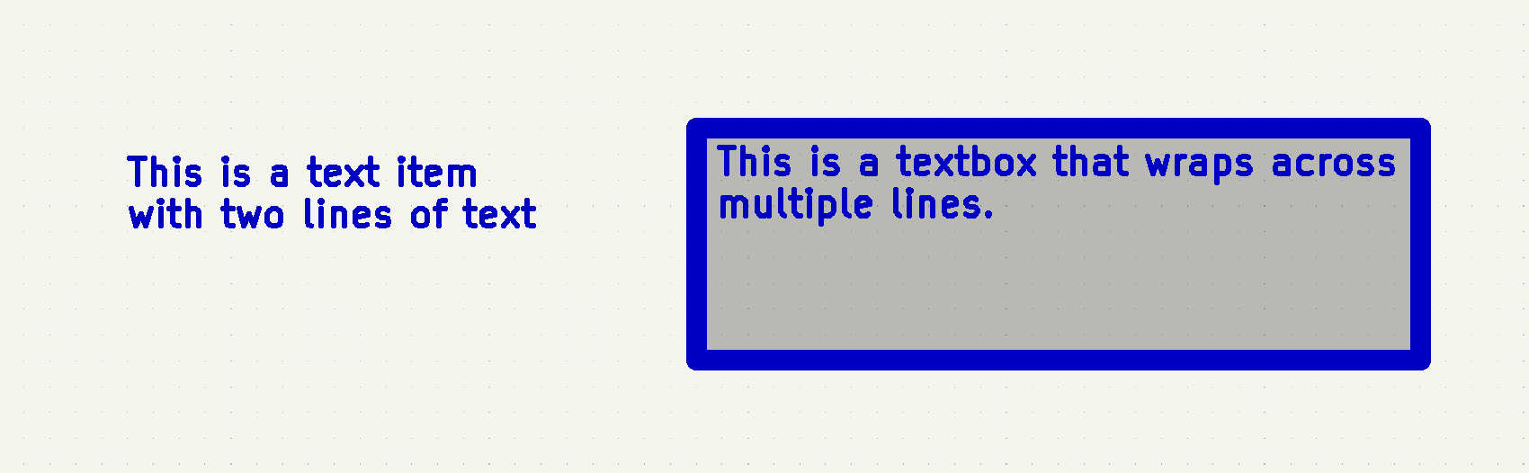
Both kinds of text item support multiline text and basic formatting features, but text boxes wrap text to fit in the outline and have additional formatting options. All text has adjustable fonts, color, size, bold and italic emphasis, left and right alignment, and vertical and horizontal orientation. Text boxes additionally support horizontal centering, vertical alignment options, and colored borders and fill.
| The default text size can be set for a schematic in Schematic Setup, and the default font can be set in Preferences. |
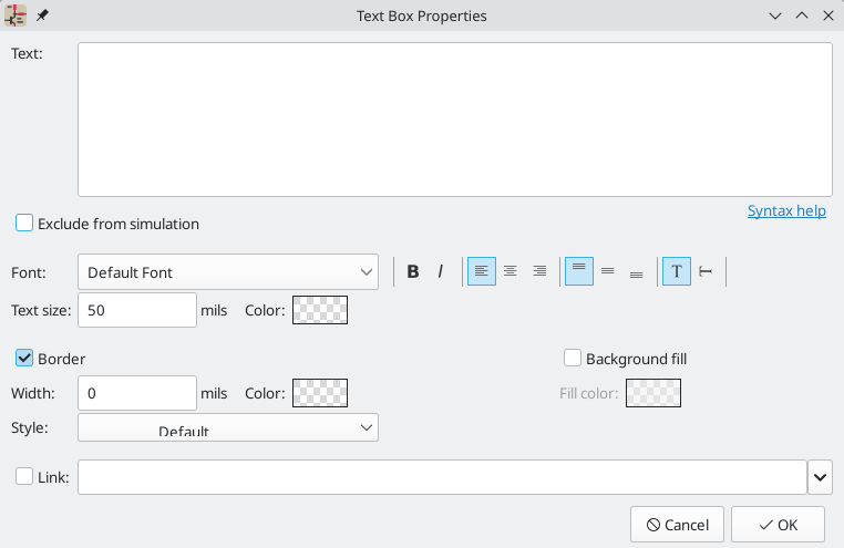
Links
Text and text boxes can be made into a link by entering a target in the Link box in the text properties. The link target can be a local file (using the file:// protocol prefix followed by the file’s path), to a website (using http:// or https:// followed by the rest of the URL), or to another page in the same schematic (using # followed by the page number). These can also be autofilled using the dropdown menu in the link target box.
Fonts
Text and text boxes support custom fonts, which are selectable with the Font dropdown in the properties dialog for the text. In addition to the KiCad font, you can use any TTF font installed on your computer.
| User fonts are not embedded in the project. If the project is opened on another computer that does not have the selected font installed, a different font will be substituted. For maximum compatibility, use the KiCad font. |
Text markup
Text supports markup for superscripts, subscripts, overbars, evaluating project variables, and accessing symbol field values.
| Feature | Markup Syntax | Result |
|---|---|---|
Superscript |
|
textsuperscript |
Subscript |
|
textsubscript |
Overbar |
|
text |
|
variable_value |
|
|
field_value of symbol refdes |
| Variables must be defined in Schematic Setup before they can be used. There are also a number of built-in system text variables. |
Simulation directives
Text and textboxes can contain simulation directives for SPICE simulations. The Exclude from simulation checkbox prevents text from being interpreted as a simulation directive.
Graphic Shapes
Graphic rectangles (![]() ), circles (
), circles (![]() ), arcs (
), arcs (![]() ), and lines (
), and lines (![]() ) can all be added using their respective buttons in the right toolbar.
) can all be added using their respective buttons in the right toolbar.
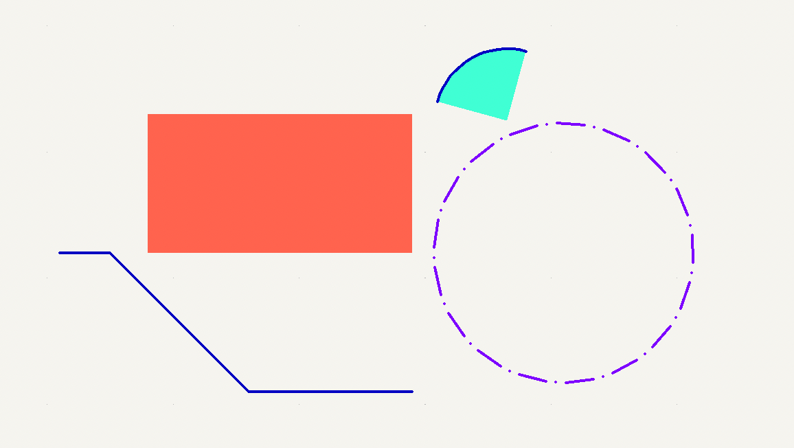
Line width, color, and style (solid, dashed, or dotted) can be configured in the properties dialog for each shape (E). Rectangles, circles, and arcs can also have a fill color set and have their outlines removed.
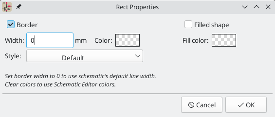
Setting a shape’s line width to 0 uses the schematic default line width, which is configurable in Schematic Setup. Spacing for line dashes is also configurable there. Removing a line or fill color uses the color theme’s graphics color, which is configurable in Preferences.
Like wires, graphic lines obey the line drawing mode setting (90 degree, 45 degree, or free angle), which you can set using the toggle buttons on the left toolbar (![]() ,
, ![]() , and
, and ![]() , respectively). Shift+Space cycles through the modes.
, respectively). Shift+Space cycles through the modes.
As with PCB tracks, the / hotkey switches line posture.
Bitmap Images
Bitmap images can be added to the schematic with the ![]() button. Images in the schematic can be moved and scaled. The properties dialog allows setting a location and scale as well as converting the image to greyscale.
button. Images in the schematic can be moved and scaled. The properties dialog allows setting a location and scale as well as converting the image to greyscale.
Bulk editing text and graphics
Properties of text and graphics can be edited in bulk using the Edit Text and Graphic Properties dialog (Tools → Edit Text and Graphic Properties…). The tool can also modify visual properties of wires and buses.
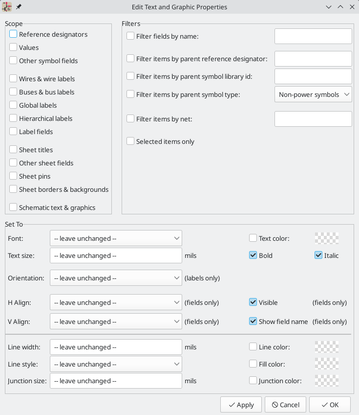
Scope and Filters
Scope settings restrict the tool to editing only certain types of objects. If no scopes are selected, nothing will be edited.
Filters restrict the tool to editing particular objects in the selected scope.
Objects will only be modified if they match all enabled and relevant filters
(some filters do not apply to certain types of objects. For example, symbol
field filters do not apply to wires and are ignored for the purpose of changing
wire properties). If no filters are enabled, all objects in the selected scope
will be modified. For filters with a text box, wildcards are supported: *
matches any number of any characters, including none, and ? matches any single
character.
Filter fields by name filters to the specified symbol, label, or sheet field.
Filter items by parent reference designator filters to fields in the symbol with the specified reference designator. Filter items by parent symbol library id filters to fields in symbols with the specified library identifier. Filter items by parent symbol type filters to fields in symbols of the selected type (power or non-power).
Filter items by net filters to wires and labels on the specified net.
Only include selected items filters to the current selection.
Editable Properties
Properties for filtered objects can be set to new values in the bottom part of the dialog.
Drop-down lists and text boxes can be set to -- leave unchanged -- to preserve existing values. Checkboxes can be checked or unchecked to enable or disable a change, but can also be toggled to a third "leave unchanged" state. Color properties must be checked to change the value; a checkerboard swatch indicates that the color will be inherited from the default value from the the schematic settings or netclass properties.
Text properties that can be modified are font, text size, text orientation (right/up/leftdown), horizontal and vertical alignment, text color, emphasis (bold and italic), and visibility of fields and field names.
Graphic and wire properties that can be modified are line width, line style (solid, dashed, and dotted lines), line color, fill color for shapes, and junction size and junction color for wire junctions.
Bloque de titulo de la hoja
The title block is edited with the Page Settings tool (![]() ).
).
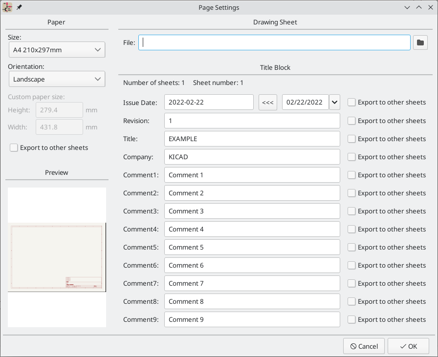
Each field in the title block can be edited, as well as the paper size and orientation. If the Export to other sheets option is checked for a field, that field will be updated in the title block of all sheets, rather than only the current sheet.
You can set the date to today’s or any other date by pressing the left arrow button next to Issue Date. Note that the date in the schematic will not be automatically updated.
A drawing sheet template file can also be selected.
The sheet number (Sheet X/Y) is automatically updated, but sheet page numbers can also be manually set using Edit → Edit Sheet Page Number….
Schematic editing convenience functions
There are several convenience features in the Schematic Editor that make some common editing and connection operations faster.
You can quickly add wires, labels, or no-connection markers to a selection of pins using the Pin Helpers tools in the right-click context menu. This can help you quickly break out unconnected pins from a symbol. By selecting Pin Helpers → Wire, the wire tool will begin drawing a wire from all selected pins at once. If you select No Connect, no-connection markers will be added to the end of each selected pin. And if you choose Net Label, Hierarchical Label, or Global Label, a label of the respective type will be placed at the end of each selected pin. Each label’s name will be set to the corresponding pin name. The new labels will remain selected, so you can easily move them away from the symbol using M or G, depending on whether you wish to maintain a wired connection between the pins and the labels.
| Pin helpers require you to select individual pins, not their parent symbol. Pins cannot be individually selected if the clicking on a pin selects the symbol option is enabled in the Editing Options pane of the Schematic Editor preferences. Therefore, this option must be disabled to use the Pin Helper tools. |
You can swap the position of two selected objects using the Swap command (S; also available in the right-click context menu). This works on symbols, labels, and graphical items. The first object is assigned the location and rotation of the second object, and vice versa. If there are more than two objects selected, the locations are cycled: the last object gets the position of the first object, the first object gets the location of the second, and so on.
| One possible use of the swap command is to exchange two units within a a symbol, for example the two amplifiers in a dual op-amp. You could also use swap with a selection of labels to quickly modify net assignments to symbol pins. In combination with cross-selection from the PCB, this can be a convenient way to make schematic changes for easier routing. This is sometimes known as pin or gate swapping. |
Schematic Setup
The Schematic Setup window is used to set schematic options that are specific to the currently active schematic. For example, the Schematic Setup window contains formatting options, electrical rule configuration, netclass setup, and schematic text variable setup.
You can import schematic settings from an existing project using the Import Settings from Another Project… button. This allows you to choose a project to use as a template and select which settings to import (formatting preferences, field name templates, pin conflict map, violation severities, and net classes).
Schematic formatting
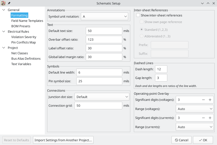
The formatting panel contains settings for the appearance of symbols, text, labels, graphics, and wires.
Symbol unit notation sets how each unit of a multi-unit symbol is referred to
in its reference designator. By default, a different letter for each unit is
appended to the reference designator with no separator, for example U1B for
the second unit of symbol U1, but this can be changed. Numbers can be used
instead of letters, and various separators can be used between the symbol
designator and the unit identifier (., -, _, or none).
Default text size sets the default text height used by the text, text box, and
label tools. Overbar offset ratio controls the vertical spacing between text
and an overbar (~{}) over that text, as a ratio of the text height.
Label offset ratio controls the vertical spacing between a local label’s text
and the attached wire, relative to the label’s text size. This also affects the
spacing between symbol pins and their pin number. Global label margin ratio
defines the size of the box around a global label, relative to the global
label’s text size. Increasing the margin may be useful to avoid overlapping text
with overbars (~{}) or letters with descenders, but this may cause closely
packed global labels to overlap with each other.
Default line width sets the default line width for symbol graphics, if the symbol does not override the default line width. Pin symbol size scales symbol pin graphic style annotations, such as the bubble on an inverted pin.
Junction dot size sets the schematic’s default wire junction dot size. The default size can be overridden by editing an individual junction dot’s properties. Connection width specifies the grid size used for the Symbol pin or wire end off connection grid ERC check. Schematics typically use a 50 mil grid for electrical connections, so this should usually remain set at 50 mils.
The Operating Point Overlay settings configure how operating point simulation results are displayed on the schematic canvas. The significant digits settings control the number of significant digits printed on voltage and current overlays. The range settings control the units used to display voltage and current measurements.
Show inter-sheet references enables or disables the display of
inter-sheet references, which are a list of page
numbers next to a global labels that link to other places in the schematic where
the same global label appears. Show own page reference controls whether the
current page is included in the list of page numbers. Standard and
abbreviated determine whether to display the complete list of page numbers or
only the first and last page numbers. The prefix and suffix fields add
optional characters before and after the list of page numbers. In the image
of an inter-sheet reference below, a prefix and suffix of [ and ],
respectively, have been added.
Dashed line appearance is controlled in the Formatting section. Dash length controls the length of dashes, while Gap length controls the spacing between dashes and dots. The dash and gap lengths are relative to the line width: a gap length of 2 means twice the width of the line.
Field name templates
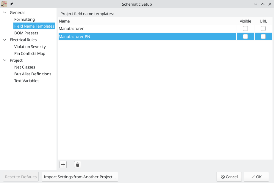
Field name templates are empty symbol fields that are automatically added to all symbols in the schematic. These can be useful when every symbol in the schematic needs additional fields beyond the fields that are defined in the library symbols, for example a field for the manufacturer’s part number.
Template fields can be set as visible or invisible, and can also be set as URL fields.
Field name templates that are defined in schematic setup apply only to the current project. Field name templates can also be defined in Preferences, which apply to all projects edited on your computer.
BOM presets
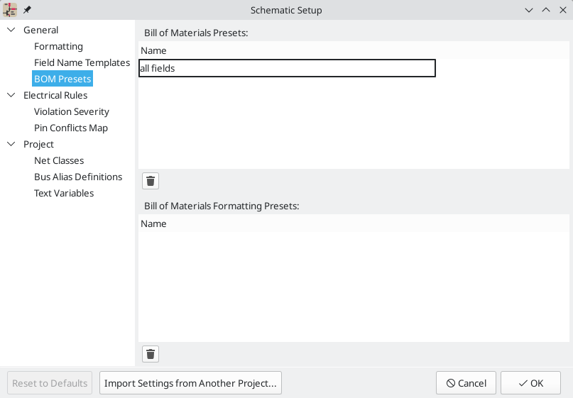
BOM presets are saved configurations for the Symbol Fields Table and BOM export tool. There are two types of presets. BOM presets configure which fields are displayed in the symbol fields table, which order they are displayed in, and how they are used to group symbols. These fields are also directly used in the BOM output. BOM formatting presets configure the output BOM file format, including which separator characters are used to separate fields. Both types of presets are created in the Symbol Fields Table, but can are listed and can be deleted here.
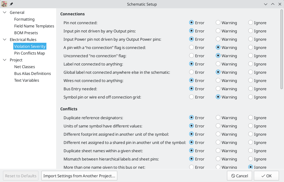
ERC violation severity and pin conflicts map
The Violation Severity panel lets you configure what types of ERC messages should be reported as Errors, Warnings, or ignored.
The Pin Conflicts Map allows you to configure connectivity rules to define electrical conditions for errors and warnings based on what types of pins are connected to each other. For example, by default an error is produced when an output pin is connected to another output pin.
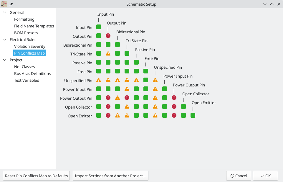
These panels are explained in more detail in the ERC section.
Net classes
The Net Classes panel allows you to manage netclasses for the project and assign nets to netclasses with patterns. Managing netclasses in this panel is equivalent to managing them in the Board Setup dialog. Nets can also be assigned to netclasses in the schematic using graphical assignments with net class directives or net labels.
Pattern-based netclass assigment is explained in more detail in the net classes section.
Bus alias definitions
The Bus Alias Definitions panel allows you to create bus aliases, which are names for groups of signals in a bus. For more information about bus aliases, see the bus alias documentation.
Text variables
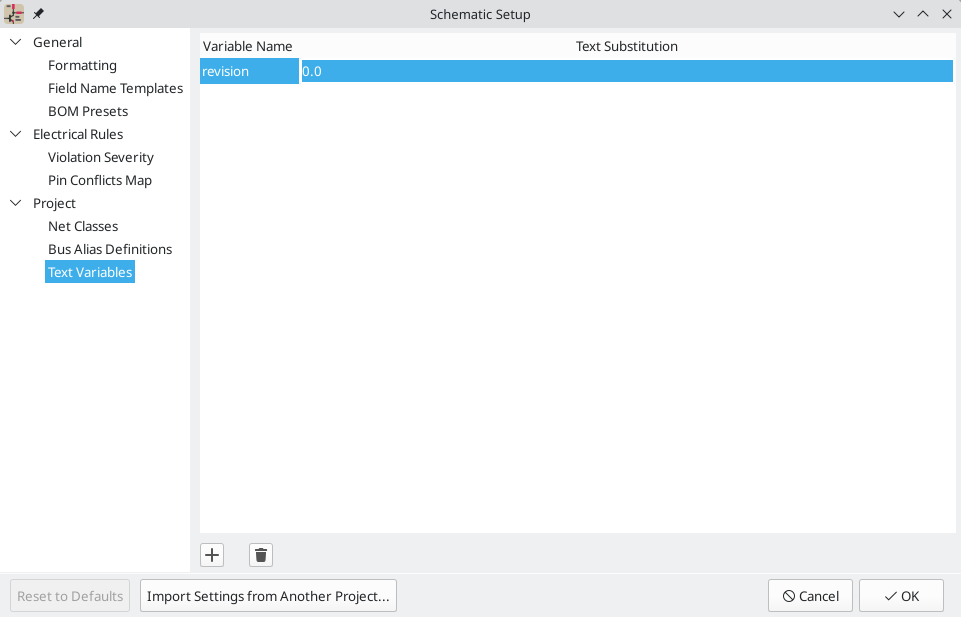
Text replacement variables can be created in the Text Variables section. These variables allow you to substitute the variable name for any text string. This substitution happens anywhere the variable name is used inside the variable replacement syntax of ${VARIABLENAME}.
For example, you could create a variable named VERSION and set the text substitution to 1.0. Now, in any text object on the PCB, you can enter ${VERSION} and KiCad will substitute 1.0. If you change the substitution to 2.0, every text object that includes ${VERSION} will be updated automatically. You can also mix regular text and variables. For example, you can create a text object with the text Version: ${VERSION} which will be substituted as Version: 1.0.
Text variables can also be created in Board Setup. Text variables are project-wide; variables created in the schematic editor are also available in the board editor, and vice versa.
There are also a number of built-in system text variables.
Opening legacy schematics
Modern versions of KiCad can always open projects created in older versions of KiCad. However, schematics created in some older versions of KiCad have special considerations that must be observed when opening them in order to prevent any data loss.
Opening KiCad 5.0 and 5.1 schematics
Modern versions of KiCad can open schematics created in versions prior to KiCad 6.0, but the cache library file (<projectname>-cache.lib) must be present to load the schematic correctly.
Since version 6.0, KiCad stores all symbols used in a project in the schematic. This means that you can open a schematic made in KiCad 6.0 or later on any computer, even if the libraries used in the project are not installed or have changed. Modern KiCad schematic files use the .kicad_sch extension.
Prior to version 6.0, KiCad did not store symbols in the schematic. Instead, KiCad stored references to the symbols and their libraries. It also stored a copy of every symbol used by the project in a separate cache library file (<projectname>-cache.lib). As long as the cache library was included with the project, the project could be distributed without the system library files, because KiCad could load any needed symbols from the cache library as a fallback if the libraries referenced in the schematic were missing. Legacy KiCad schematic files use the .sch extension.
When you open a legacy schematic, KiCad will look in the cache library to find all of the symbols used in the schematic in the cache library. When you save the legacy schematic, KiCad will save it as a new file in the modern schematic format (.kicad_sch), with the necessary symbols embedded in the schematic itself. The original legacy schematic and the cache library will remain, unmodified, but they are no longer necessary once the schematic has been saved in the modern format.
| Projects created in KiCad prior to version 6.0 must have a cache library. If the cache library is missing, the schematic will lose symbol information if the system symbol libraries are modified, reorganized, moved, or deleted. The libraries included with legacy versions of KiCad are substantially different than the modern KiCad libraries, so in practice KiCad will almost always fail to open legacy projects unless the cache library is present. |
When you open a legacy schematic, KiCad may display the Project Rescue Helper dialog. This means that one or more symbols in the cache library do not match the corresponding symbol in the external library. The dialog helps you "rescue" symbols from the cache library into your schematic, if desired. You can also open the rescue dialog at any time using Tools → Rescue Symbols…. The cache library file must be present in order to use the rescue tool.
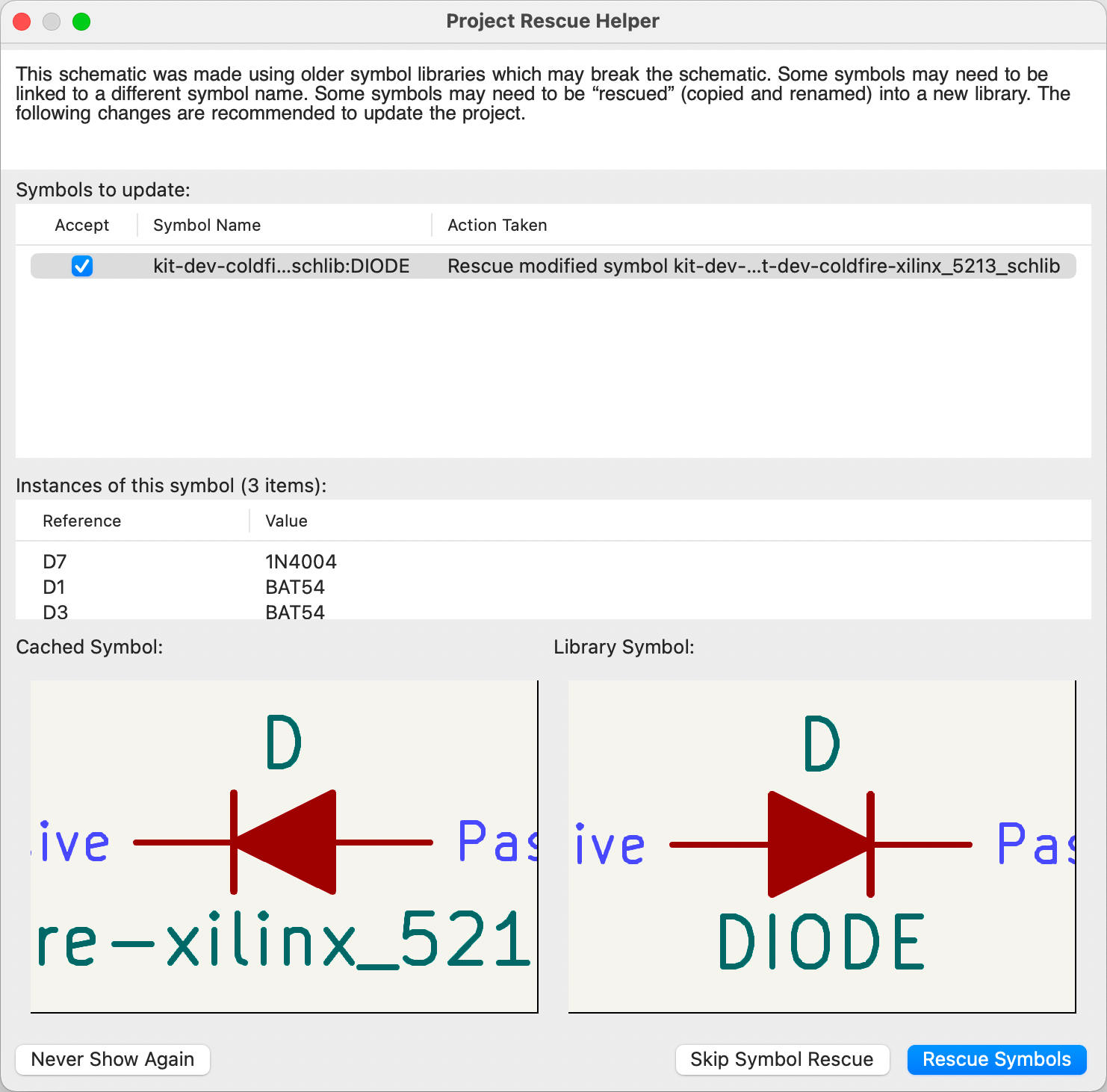
The rescue dialog lists all symbols that don’t match between the cache library and the external symbol library. The discrepancy can be because:
-
the cached symbol or the library symbol has been modified, so the two symbols no longer match, or
-
the cached symbol does not have a corresponding symbol in the symbol library, because the symbol or library was moved, renamed, deleted, or is not present on the current computer.
For each symbol in the list, selecting the symbol displays the reference designator and value for each instance of the symbol, and shows a visual preview of the symbol. If a corresponding symbol exists in the system symbol library, the dialog shows both copies of the symbol for comparison. If the symbol only exists in the cache library, the dialog only shows the cached symbol.
In this example, the project originally used a diode with the cathode facing left, but the library now contains one with the cathode facing right. This change would break the design, so it would be important to use the cached symbol as the original designer intended.
Pressing Rescue Symbols here will cause the selected symbols from the cache library to be saved into a special rescue library (<projectname>-rescue.kicad_sym). The corresponding symbols in the schematic will be updated to use the newly rescued symbols. Any unselected symbols will not be rescued, but their symbol linkage can be updated in the schematic later.
Alternatively, pressing Skip Symbol Rescue will exit the dialog without rescuing any symbols. KiCad will use the versions of the symbols found in the external libraries. You can run the rescue function again with Tools → Rescue Symbols…, or manually edit symbol linkage in the symbol’s properties.
If you would prefer not to see this dialog, you can press Never Show Again. This has the same effect as pressing Skip Symbol Rescue for the current schematic and all future schematics.
If a symbol in a legacy schematic cannot be found in either the cache library or the external library, KiCad cannot rescue that symbol. A placeholder symbol is inserted into the schematic in its place, as shown below.
You can attempt to remap these orphaned symbols using the Change Symbols or Edit Symbol Library Links dialogs, but either option may require manual corrections to the schematic. These tools are explained in more detail in the Updating and exchanging symbols section.
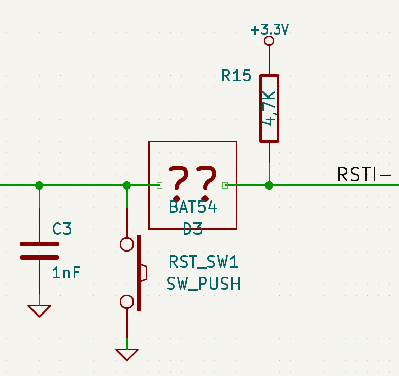
Opening pre-5.0 schematics
Modern versions of KiCad can open schematics created in versions prior to KiCad 5.0, but you will need to go through a symbol remapping process to open the schematic without losing symbol information.
Since version 5.0, KiCad schematics refer to specific symbols using both the symbol and library name. Even if multiple libraries each contain a symbol with the same name, the designer’s intended symbol is unambiguously specified.
Prior to version 5.0, KiCad schematics stored only the symbol name, not the library name. Symbols in the schematic were indirectly mapped back to the original library by searching through the project’s library list for a matching symbol. When you open a pre-5.0 schematic, KiCad will attempt to automatically "remap" the symbols so that each bare symbol name is replaced with a fully-specified symbol library and symbol name pair. The original schematics will be backed up in a rescue-backup folder.
You can skip the automatic remapping, but you will need to remap the symbols yourself using the Change Symbols dialog. You can also re-run the Remap Symbols tool using Tools → Remap Legacy Library Symbols….