sudo add-apt-repository ppa:js-reynaud/ppa-kicad
sudo aptitude update && sudo aptitude safe-upgrade
sudo aptitude install kicad kicad-doc-en
Guía Esencial y concisa para dominar KiCad en el desarrollo exitoso de sofisticadas placas de circuito impreso.
Copyright
This document is Copyright © 2010-2018 by its contributors as listed below. You may distribute it and/or modify it under the terms of either the GNU General Public License (http://www.gnu.org/licenses/gpl.html), version 3 or later, or the Creative Commons Attribution License (http://creativecommons.org/licenses/by/3.0/), version 3.0 or later.
Todas las marcas mencionadas en esta guía pertenecen a sus legítimos propietarios.
Contribuidores
David Jahshan, Phil Hutchinson, Fabrizio Tappero, Christina Jarron, Melroy van den Berg.
Traducción
Antonio Morales <[email protected]>, 2015-2016
Realimentación
Por favor dirija cualquier reporte de fallo, sugerencia o nuevas versiones a:
-
About KiCad documentation: https://gitlab.com/kicad/services/kicad-doc/issues
-
Acerca del software KiCad: https://gitlab.com/kicad/code/kicad/issues
-
About KiCad software internationalization (i18n): https://gitlab.com/kicad/code/kicad-i18n/issues
Fecha de publicación
16 de Mayo de 2015.
Introducción a KiCad
KiCad es una herramienta software open-source para la creación de diagramas electrónicos y diseño de placas de circuito impreso. Bajo su singular fachada, KiCad incorpora un elegante conjunto con las siguientes herramientas de software independientes:
| Program name | Description | File extension |
|---|---|---|
KiCad |
Project manager |
*.pro |
Eeschema |
Schematic and component editor |
*.sch, *.lib, *.net |
Pcbnew |
Circuit board and footprint editor |
*.kicad_pcb, *.kicad_mod |
GerbView |
Gerber and drill file viewer |
\*.g\*, *.drl, etc. |
Bitmap2Component |
Convert bitmap images to components or footprints |
*.lib, *.kicad_mod, *.kicad_wks |
PCB Calculator |
Calculator for components, track width, electrical spacing, color codes, and more… |
None |
Pl Editor |
Page layout editor |
*.kicad_wks |
| The file extension list is not complete and only contains a subset of the files that KiCad supports. It is useful for the basic understanding of which files are used for each KiCad application. |
KiCad puede considerarse lo suficientemente maduro como para ser utilizado en el desarrollo exitoso y mantenimiento de tarjetas electrónicas complejas.
KiCad no presenta ninguna limitación en cuanto al tamaño de la placa de circuito y puede gestionar fácilmente hasta 32 capas de cobre, hasta 14 capas técnicas y hasta 4 capas auxiliares. KiCad puede crear todos los archivos necesarios para la construcción de placas de circuito impreso, archivos Gerber para foto-plotters, archivos para taladrado, archivos de ubicación de los componentes y mucho más.
Al ser de código abierto (licencia GPL), KiCad representa la herramienta ideal para proyectos orientados a la creación de equipos electrónicos con estilo open-source.
On the Internet, the homepage of KiCad is:
Downloading and installing KiCad
KiCad runs on GNU/Linux, Apple macOS and Windows. You can find the most up to date instructions and download links at:
| KiCad stable releases occur periodically per the KiCad Stable Release Policy. New features are continually being added to the development branch. If you would like to take advantage of these new features and help out by testing them, please download the latest nightly build package for your platform. Nightly builds may introduce bugs such as file corruption, generation of bad Gerbers, etc., but it is the goal of the KiCad Development Team to keep the development branch as usable as possible during new feature development. |
Bajo GNU/Linux
Se pueden encontrar Versiones estables de KiCad en la mayoría de los gestores de paquetes de las distintas distribuciones como kicad y kicad-doc. Si su distribución no proporciona la última versión estable, por favor, siga las instrucciones para versiones inestables y seleccione e instale la última versión estable.
En Ubuntu, la forma más fácil de instalar una versión inestable de KiCad es a través PPA y Aptitude. Escriba lo siguiente en una terminal:
Under Debian, the easiest way to install backports build of KiCad is:
# Set up Debian Backports
echo -e "
# stretch-backports
deb http://ftp.us.debian.org/debian/ stretch-backports main contrib non-free
deb-src http://ftp.us.debian.org/debian/ stretch-backports main contrib non-free
" | sudo tee -a /etc/apt/sources.list > /dev/null

# Run an Update & Install KiCad
sudo apt-get update
sudo apt-get install -t stretch-backports kicad
Bajo Fedora la forma más fácil de instalar una versión inestable es a través copr. Para instalar KiCad vía copr escriba lo siguiente dentro de copr:
sudo dnf copr enable @kicad/kicad
sudo dnf install kicad
Como alternativa, puede descargar e instalar una versión pre-compilada de KiCad, o descargar directamente el código fuente, compilar e instalar KiCad.
Under Apple macOS
Stable builds of KiCad for macOS can be found at: https://downloads.kicad.org/kicad/macos/explore/stable
Unstable nightly development builds can be found at: https://downloads.kicad.org/kicad/macos/explore/nightlies
Bajo Windows
Stable builds of KiCad for Windows can be found at: https://downloads.kicad.org/kicad/windows/explore/stable
For Windows you can find nightly development builds at: https://downloads.kicad.org/kicad/windows/explore/nightlies
Soporte
Si tiene ideas, comentarios o preguntas, o si simplemente necesita ayuda:
-
Visit the Forum
-
Join users on IRC or Discord
-
Watch Tutorials
Flujo de trabajo en KiCad
Despite its similarities with other PCB design software, KiCad is characterised by a unique workflow in which schematic components and footprints are separate. Only after creating a schematic are footprints assigned to the components.
Overview
The KiCad workflow is comprised of two main tasks: drawing the schematic and laying out the board. Both a schematic component library and a PCB footprint library are necessary for these two tasks. KiCad includes many components and footprints, and also has the tools to create new ones.
In the picture below, you see a flowchart representing the KiCad workflow. The flowchart explains which steps you need to take, and in which order. When applicable, the icon is added for convenience.
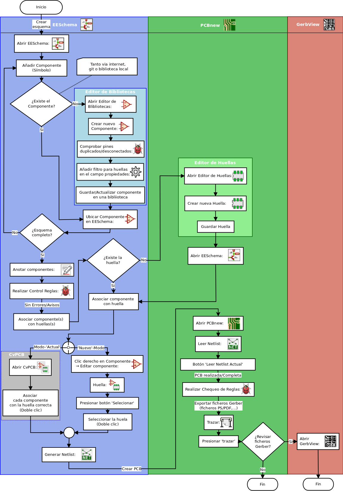
For more information about creating a component, read Making schematic symbols. And for information about how to create a new footprint, see Making component footprints.
Quicklib is a tool that allows you to quickly create KiCad library components with a web-based interface. For more information about Quicklib, refer to Making Schematic Components With Quicklib.
Anotado hacia adelante y hacia atrás
Once an electronic schematic has been fully drawn, the next step is to transfer it to a PCB. Often, additional components might need to be added, parts changed to a different size, net renamed, etc. This can be done in two ways: Forward Annotation or Backward Annotation.
Forward Annotation is the process of sending schematic information to a corresponding PCB layout. This is a fundamental feature because you must do it at least once to initially import the schematic into the PCB. Afterwards, forward annotation allows sending incremental schematic changes to the PCB. Details about Forward Annotation are discussed in the section Forward Annotation.
Backward Annotation is the process of sending a PCB layout change back to its corresponding schematic. Two common causes for Backward Annotation are gate swaps and pin swaps. In these situations, there are gates or pins which are functionally equivalent, but it may only be during layout that there is a strong case for choosing the exact gate or pin. Once the choice is made in the PCB, this change is then pushed back to the schematic.
Using KiCad
Shortcut keys
KiCad has two kinds of related but different shortcut keys: accelerator keys and hotkeys. Both are used to speed up working in KiCad by using the keyboard instead of the mouse to change commands.
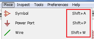
Accelerator keys
Accelerator keys have the same effect as clicking on a menu or toolbar icon: the command will be entered but nothing will happen until the left mouse button is clicked. Use an accelerator key when you want to enter a command mode but do not want any immediate action.
Accelerator keys are shown on the right side of all menu panes:
Hotkeys
A hotkey is equal to an accelerator key plus a left mouse click. Using a hotkey starts the command immediately at the current cursor location. Use a hotkey to quickly change commands without interrupting your workflow.
To view hotkeys within any KiCad tool go to Help → List Hotkeys or press Ctrl+F1:
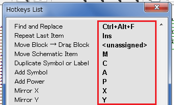
You can edit the assignment of hotkeys, and import or export them, from the Preferences → Hotkeys Options menu.
| In this document, hotkeys are expressed with brackets like this: [a]. If you see [a], just type the "a" key on the keyboard. |
Example
Consider the simple example of adding a wire in a schematic.
To use an accelerator key, press "Shift + W" to invoke the "Add wire" command (note the cursor will change). Next, left click on the desired wire start location to begin drawing the wire.
With a hotkey, simply press [w] and the wire will immediately start from the current cursor location.
Dibujar esquemas electrónicos
En esta sección vamos a aprender a dibujar un esquema electrónico utilizando KiCad.
Usando Eeschema
-
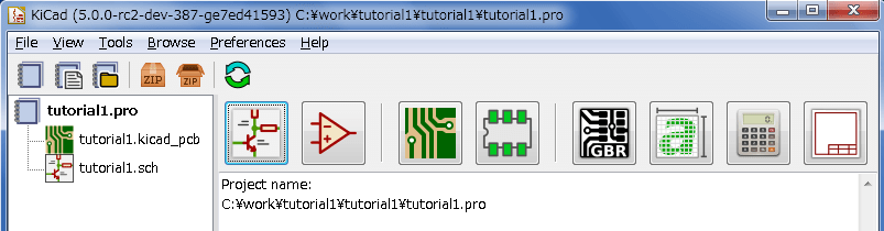
En Windows ejecute kicad.exe. Bajo Linux escriba 'kicad' en una terminal. Ahora se encuentra en la ventana principal del gestor del proyectos de KiCad. Desde aquí tiene acceso a ocho herramientas de software independientes: Eeschema, Schematic Library Editor, Pcbnew, PCB Footprint Editor, GerbView, Bitmap2Component, PCB Calculator y Pl Editor. Consulte la tabla de flujo de trabajo para obtener una idea de cómo se utilizan las principales herramientas.
-
Create a new project: File → New → Project. Name the project file 'tutorial1'. The project file will automatically take the extension ".pro". The exact appearance of the dialog depends on the used platform, but there should be a checkbox for creating a new directory. Let it stay checked unless you already have a dedicated directory. All your project files will be saved there.
-
Comencemos creando un esquema. Inicie el editor de esquemas Eeschema,
 . Es el primer botón de la izquierda.
 -
Click on the 'Page Settings' icon
 on the top toolbar. Set the appropriate 'paper size' ('A4','8.5x11' etc.) and enter the Title as 'Tutorial1'. You will see that more information can be entered here if necessary. Click OK. This information will populate the schematic sheet at the bottom right corner. Use the mouse wheel to zoom in. Save the whole schematic: File → Save
 -
We will now place our first component. Click on the 'Place symbol' icon
 in the right toolbar. You may also press the 'Add Symbol' hotkey [a].
 -
Click on the middle of your schematic sheet. A Choose Symbol window will appear on the screen. We’re going to place a resistor. Search / filter on the 'R' of Resistor. You may notice the 'Device' heading above the Resistor. This 'Device' heading is the name of the library where the component is located, which is quite a generic and useful library.
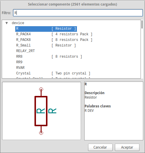
-
Double click on it. This will close the 'Choose Symbol' window. Place the component in the schematic sheet by clicking where you want it to be.
-
Haga clic en el icono de la lupa para hacer zoom sobre el componente. También puede utilizar la rueda del ratón para acercar y alejar la imagen. Pulse el botón central del ratón (rueda) para desplazarse horizontal y verticalmente.
-
Try to hover the mouse over the component 'R' and press [r]. The component should rotate. You do not need to actually click on the component to rotate it.
Sometimes, if your mouse is also over something else, a menu will appear. You will see the Clarify Selection menu often in KiCad; it allows working on objects that are on top of each other. In this case, tell KiCad you want to perform the action on the 'Symbol …R…' if the menu appears. -
Right click in the middle of the component and select Properties → Edit Value. You can achieve the same result by hovering over the component and pressing [v]. Alternatively, [e] will take you to the more general Properties window. Notice how the right-click menu below shows the hotkeys for all available actions.
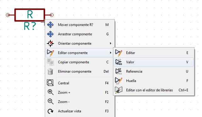
-
The Edit Value Field window will appear. Replace the current value 'R' with '1 k'. Click OK.
Do not change the Reference field (R?), this will be done automatically later on. The value above the resistor should now be '1 k'. 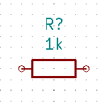
-
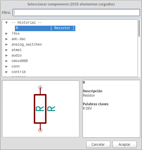
To place another resistor, simply click where you want the resistor to appear. The symbol selection window will appear again.
-
La resistencia que eligió previamente se encuentra ahora en la lista Historial, apareciendo como 'R'. Haga clic en Aceptar y coloque el componente.
-
In case you make a mistake and want to delete a component, right click on the component and click 'Delete'. This will remove the component from the schematic. Alternatively, you can hover over the component you want to delete and press [Delete].
-
You can also duplicate a component already on your schematic sheet by hovering over it and pressing [c]. Click where you want to place the new duplicated component.
-
Right click on the second resistor. Select 'Drag'. Reposition the component and left click to drop. The same functionality can be achieved by hovering over the component and by pressing [g]. [r] will rotate the component while [x] and [y] will flip it about its x- or y-axis.
Right-Click → Move or [m] is also a valuable option for moving anything around, but it is better to use this only for component labels and components yet to be connected. We will see later on why this is the case. -
Edit the second resistor by hovering over it and pressing [v]. Replace 'R' with '100'. You can undo any of your editing actions with Ctrl+Z.
-
Change the grid size. You have probably noticed that on the schematic sheet all components are snapped onto a large pitch grid. You can easily change the size of the grid by Right-Click → Grid. In general, it is recommended to use a grid of 50.0 mils for the schematic sheet.
-
We are going to add a component from a library that may not be configured in the default project. In the menu, choose Preferences → Manage Symbol Libraries. In the Symbol Libraries window you can see two tabs: Global Libraries and Project Specific Libraries. Each one has one sym-lib-table file. For a library (.lib file) to be available it must be in one of those sym-lib-table files. If you have a library file in your file system and it’s not yet available, you can add it to either one of the sym-lib-table files. For practice we will now add a library which already is available.
-
Select the Project Specific table. Click the file browser button below the table. You need to find where the official KiCad libraries are installed on your computer. Look for a
librarydirectory containing a hundred of.dcmand.libfiles. Try inC:\Program Files (x86)\KiCad\share\(Windows) and/usr/share/kicad/library/(Linux). When you have found the directory, choose and add the 'MCU_Microchip_PIC12.lib' library and close the window. It will be added to the end of of the list. Now click its nickname and change it to 'microchip_pic12mcu'. Close the Symbol Libraries window with OK. -
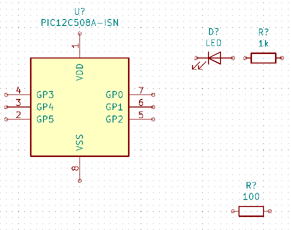
Repeat the add-component steps, however this time select the 'microchip_pic12mcu' library instead of the 'Device' library and pick the 'PIC12C508A-ISN' component.
-
Hover the mouse over the microcontroller component. Notice that [x] and [y] again flip the component. Keep the symbol mirrored around the Y axis so that the pins G0 and G1 point to right.
-
Repeat the add-component steps, this time choosing the 'Device' library and picking the 'LED' component from it.
-
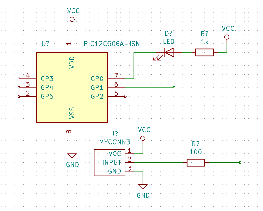
Organice todos los componentes en su esquema con la distribución que se muestra debajo.
-
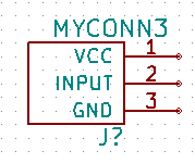
We now need to create the schematic component 'MYCONN3' for our 3-pin connector. You can jump to the section titled Make Schematic Symbols in KiCad to learn how to make this component from scratch and then return to this section to continue with the board.
-
You can now place the freshly made component. Press [a] and pick the 'MYCONN3' component in the 'myLib' library.
-
The component identifier 'J?' will appear under the 'MYCONN3' label. If you want to change its position, right click on 'J?' and click on 'Move Field' (equivalent to [m]). It might be helpful to zoom in before/while doing this. Reposition 'J?' under the component as shown below. Labels can be moved around as many times as you please.
-
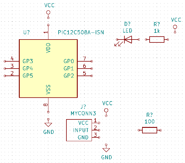
It is time to place the power and ground symbols. Click on the 'Place power port' button
 on the right toolbar. Alternatively, press [p]. In the component selection window, scroll down and select 'VCC' from the 'power' library. Click OK.
 -
Click above the pin of the 1 k resistor to place the VCC part. Click on the area above the microcontroller 'VDD'. In the 'Component Selection history' section select 'VCC' and place it next to the VDD pin. Repeat the add process again and place a VCC part above the VCC pin of 'MYCONN3'. Move references and values out of the way if needed.
-
Repeat the add-pin steps but this time select the GND part. Place a GND part under the GND pin of 'MYCONN3'. Place another GND symbol on the left of the VSS pin of the microcontroller. Your schematic should now look something like this:
-
Ahora, conectaremos todos nuestros componentes. Haga clic en el icono 'Añadir hilo'
 en la barra de herramientas derecha.
Be careful not to pick 'Place bus', which appears directly beneath this button but has thicker lines. The section Bus Connections in KiCad will explain how to use a bus section. -
Click on the little circle at the end of pin 7 of the microcontroller and then click on the little circle on pin 1 of the LED. Click once when you are drawing the wire to create a corner. You can zoom in while you are placing the connection.
If you want to reposition wired components, it is important to use [g] (to grab) and not [m] (to move). Using grab will keep the wires connected. Review step 24 in case you have forgotten how to move a component. 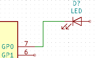
-
Repita este proceso y conecte el resto de componentes como se muestra a continuación. Para terminar un hilo simplemente haga doble clic. Al conectar los símbolos VCC y GND, el hilo debe tocar la parte inferior del símbolo VCC y el centro de la parte superior del símbolo GND. Vea la siguiente imagen.
-
We will now consider an alternative way of making a connection using labels. Pick a net labelling tool by clicking on the 'Place net label' icon
 on the right toolbar. You can also use [l].
 -
Click in the middle of the wire connected to pin 6 of the microcontroller. Name this label 'INPUT'. The label is still an independent item which you can for example move, rotate and delete. The small anchor rectangle of the label must be exactly on a wire or a pin for the label to take effect.
-
Siga el mismo procedimiento para colocar otra etiqueta en el hilo a la derecha de la resistencia de 100 ohmios. Nombrela también como "INPUT". Al tener las dos etiquetas el mismo nombre, se crea una conexión invisible entre el pin 6 del PIC y la resistencia de 100 ohmios. Esta es una técnica útil para conectar hilos en un diseño complejo donde el dibujo de las líneas haría todo el esquema desordenado. Para colocar una etiqueta no necesita necesariamente un hilo, simplemente puede colocar la etiqueta sobre un pin del componente.
-
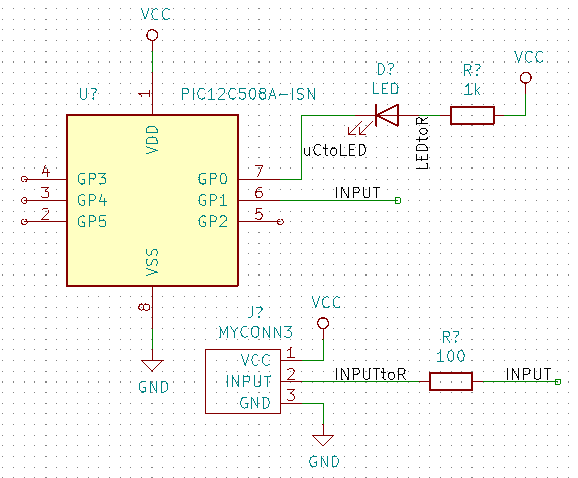
Las etiquetas también pueden ser utilizadas simplemente para etiquetar hilos con fines informativos. Coloque una etiqueta en el pin 7 del PIC. Introduzca el nombre de 'uCtoLED'. Nombre del hilo entre la resistencia y el LED como 'LEDtoR'. Nombre el hilo entre 'MYCONN3' y la resistencia como "INPUTtoR '.
-
No tiene porque etiquetar las líneas de VCC y GND, dado que estas están implícitamente etiquetadas a través de los puertos de alimentación a los que están conectadas.
-
Abajo puede ver como debería ser su resultado final.
-
Tratemos ahora los hilos no conectados. Cualquier pin o hilo que no esté conectado generará una advertencia durante el chequeo realizado por KiCad. Para evitar estas advertencias puede indicar al programa que los cables no conectados son deliberados o indicar manualmente cada cable o pin sin conectar como desconectado.
-
Click on the 'Place no connection flag' icon
 on the right toolbar. Click on pins 2, 3, 4 and 5. An X will appear to signify that the lack of a wire connection is intentional.
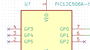
-
Algunos componentes tienen pines de alimentación no visibles. Puede hacerlos visibles haciendo clic en el icono 'Mostrar pines ocultos'
 en la barra de herramientas izquierda. Los pines de alimentación ocultos se conectan automáticamente si se respetan los nombres VCC y GND. En general, debería evitar hacer pines de alimentación ocultos.
 -
It is now necessary to add a 'Power Flag' to indicate to KiCad that power comes in from somewhere. Press [a] and search for 'PWR_FLAG' which is in 'power' library. Place two of them. Connect them to a GND pin and to VCC as shown below.
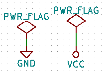
This will avoid the classic schematic checking warning: Pin connected to some other pins but no pin to drive it. -
Sometimes it is good to write comments here and there. To add comments on the schematic use the 'Place text' icon
 on the right toolbar.
 -
All components now need to have unique identifiers. In fact, many of our components are still named 'R?' or 'J?'. Identifier assignation can be done automatically by clicking on the 'Annotate schematic symbols' icon
 on the top toolbar.
 -
In the Annotate Schematic window, select 'Use the entire schematic' and click on the 'Annotate' button. Click 'Close'. Notice how all the '?' have been replaced with numbers. Each identifier is now unique. In our example, they have been named 'R1', 'R2', 'U1', 'D1' and 'J1'.
-
Revisemos ahora los errores de nuestro esquema. Haga clic en el icono 'Comprobar Reglas Eléctricas'
 en la barra de herramientas superior. Haga clic en el botón 'Ejecutar'. Se genera un informe que le muestra los errores o advertencias tales como cables desconectados. Debe tener 0 Errores y 0 Advertencias. En caso de errores o advertencias, una pequeña flecha verde aparecerá en el esquema en la posición donde se encuentra el error o la advertencia. Marque 'Crear archivo de informe ERC' y pulse el botón 'Ejecutar' de nuevo para recibir más información acerca de los errores.
If you have a warning with "No default editor found, you must choose it", try setting the path to c:\windows\notepad.exe(windows) or/usr/bin/gedit(Linux). -
The schematic is now finished. We can now create a Netlist file to which we will add the footprint of each component. Click on the 'Generate netlist' icon
 on the top toolbar. Click on the 'Generate Netlist' button and save under the default file name.
Netlist was necessary in previous versions of KiCad. In the recent versions you can ignore it and instead use Tools → Update PCB from Schematic. If you do that you have to assign footprints to symbols first. -
Después de generar el archivo de Netlist, haga clic en el icono 'Ejecutar Cvpcb'
 en la barra de herramientas superior. Si aparece una ventana de error indicando que falta algún archivo, simplemente ignórela y haga clic en Aceptar.
There are many more ways to add footprints to symbols.
-
Right click on a symbol → Properties → Edit Footprint Double click on a symbol, or right click on a symbol → Properties → Edit Properties → Footprint
-
Tools → Edit Symbol Fields Check Show footprint previews in symbol chooser in Eeschema’s preferences and select the footprint when you select a new symbol to place
-
-
Cvpcb allows you to link all the components in your schematic with footprints in the KiCad library. The pane on the center shows all the components used in your schematic. Here select 'D1'. In the pane on the right you have all the available footprints, here scroll down to 'LED_THT:LED-D5.0mm' and double click on it.
-
Es posible que el panel de la derecha muestre solamente un subgrupo seleccionado de huellas disponibles. Esto se debe a que KiCad está tratando de sugerirle un subconjunto de huellas adecuados. Haga clic en los
 ,
,  y
y  para activar o desactivar estos filtros.
 -
For 'U1' select the 'Package_DIP:DIP-8_W7.62mm' footprint. For 'J1' select the 'Connector:Banana_Jack_3Pin' footprint. For 'R1' and 'R2' select the 'Resistor_THT:R_Axial_DIN0207_L6.3mm_D2.5mm_P2.54mm_Vertical' footprint.
-
If you are interested in knowing what the footprint you are choosing looks like, you can click on the 'View selected footprint' icon
 for a preview of the current footprint.
 -
You are done. You can save the schematic now by clicking File → Save Schematic or with the button 'Apply, Save Schematic & Continue'.
-
You can close Cvpcb and go back to the Eeschema schematic editor. If you didn’t save it in Cvpcb save it now by clicking on File → Save. Create the netlist again. Your netlist file has now been updated with all the footprints. Note that if you are missing the footprint of any device, you will need to make your own footprints. This will be explained in a later section of this document.
Now every symbol has a footprint. Instead of the net list and the next two steps you can use Tools → Update PCB from Schematic. If you do that, Pcbnew is opened with Update PCB from Schematic dialog. Click Update PCB. Then You can follow the instructions in the Pcbnew section of this tutorial. -
Switch to the KiCad project manager. You can see the net list file in the file list.
-
El archivo netlist describe todos los componentes y las conexiones de sus respectivos pines. El archivo netlist es en realidad un archivo de texto que se puede inspeccionar, editar o realizar scripts.
Los archivos de la bibliotecas (*.Lib) son también archivos de texto y por tanto fácilmente editables o analizables mediante scripts. -
To create a Bill Of Materials (BOM), go to the Eeschema schematic editor and click on the 'Generate bill of materials' icon
 on the top toolbar. By default there is no plugin active. You add one, by clicking on Add Plugin button. Select the *.xsl file you want to use, in this case, we select bom2csv.xsl.
Linux:
If xsltproc is missing, you can download and install it with:
sudo apt-get install xsltproc
for a Debian derived distro like Ubuntu, or
sudo yum install xsltproc
for a RedHat derived distro. If you use neither of the two kind of distro, use your distro package manager command to install the xsltproc package.
xsl files are located at: /usr/lib/kicad/plugins/.
Apple OS X:
If xsltproc is missing, you can either install the Apple Xcode tool from the Apple site that should contain it, or download and install it with:
brew install libxslt
xsl files are located at: /Library/Application Support/kicad/plugins/.
Windows:
xsltproc.exe and the included xsl files will be located at <KiCad install directory>\bin and <KiCad install directory>\bin\scripting\plugins, respectively.
All platforms:
You can get the latest bom2csv.xsl via:
KiCad genera automáticamente el comando, por ejemplo:xsltproc -o "%O" "/home/<user>/kicad/eeschema/plugins/bom2csv.xsl" "%I"
Es posible que desee añadir la extensión, cambie esta línea de comandos a:xsltproc -o "%O.csv" "/home/<user>/kicad/eeschema/plugins/bom2csv.xsl" "%I"
Pulse el botón Ayuda para obtener más información.
-
Ahora pulse 'Generar'. El archivo (mismo nombre que su proyecto) se encuentra en la carpeta del proyecto. Abra el archivo *.csv Con LibreOffice Calc o Excel. Aparecerá una ventana de importación, pulse Aceptar.
Ya está listo para pasar a la parte diseño de la PCB, que se presenta en la siguiente sección. Sin embargo, antes de seguir adelante vamos a echar un vistazo rápido a la forma de conectar los pines de componentes utilizando buses.
Conexiones mediante buses en KiCad
A veces, puede que necesite conectar varios pines consecutivos de un componente A con algunos otros pines consecutivos de otro componente B. En este caso, tiene dos opciones: el método de etiquetado que ya hemos visto o el uso de una conexión mediante un bus. Veamos cómo hacerlo.
-
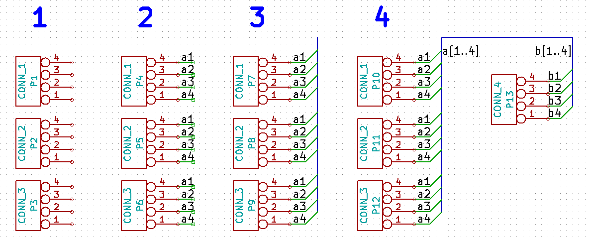
Let us suppose that you have three 4-pin connectors that you want to connect together pin to pin. Use the label option (press [l]) to label pin 4 of the P4 part. Name this label 'a1'. Now press [Insert] to have the same item automatically added on the pin below pin 4 (PIN 3). Notice how the label is automatically renamed 'a2'.
-
Press [Insert] two more times. This key corresponds to the action 'Repeat last item' and it is an infinitely useful command that can make your life a lot easier.
-
Repita la misma acción de etiquetado en los otros dos conectores CONN_2 y CONN_3 y ya está. Si continúa y realiza una PCB verá que los tres conectores están conectados entre sí. La Figura 2 muestra el resultado de lo que hemos descrito. Con fines estéticos también es posible añadir una serie de 'conectores de hilo a bus' utilizando el icono
 y líneas de bus utilizando el icono
  , como se muestra en la Figura 3. Tenga en cuenta, sin embargo, que esto no añade ningún efecto sobre la PCB.
 -
Cabe señalar que los hilos cortos unidos a los pines en la figura 2 no son estrictamente necesarios. De hecho, las etiquetas se podrían haber aplicado directamente a los pines.
-
Demos un paso más allá y supongamos que tenemos un cuarto conector llamado CONN_4 y, por alguna razón, su etiquetado ha de ser un poco diferente (b1, b2, b3, b4). Ahora queremos conectar el Bus a con el Bus b mediante una asignación pin a pin. Queremos realizarlo sin usar etiquetado de pin (que también es posible), sino mediante el etiquetado en la línea del bus, con una etiqueta por bus.
-
Conecte y etiquete CONN_4 utilizando el método de etiquetado explicado anteriormente. Nombre los pines B1, B2, B3 y B4. Conecte los pines a una serie de 'conectores de entrada a bus' utilizando el icono
y a un bus utilizando el icono:  . Vea la Figura 4.
 -
Put a label (press [l]) on the bus of CONN_4 and name it 'b[1..4]'.
-
Put a label (press [l]) on the previous bus and name it 'a[1..4]'.
-
Lo que ahora podemos hacer es conectar el bus a[1..4] con el autobús b[1..4] utilizando una línea de bus con el botón
. -
Mediante la conexión de los dos buses juntos, pin a1 se conectará automáticamente al pin b1, a2 se conectará a b2 y así sucesivamente. La figura 4 muestra como sería el resultado final.
The 'Repeat last item' option accessible via [Insert] can be successfully used to repeat period item insertions. For instance, the short wires connected to all pins in Figure 2, Figure 3 and Figure 4 have been placed with this option. -
The 'Repeat last item' option accessible via [Insert] has also been extensively used to place the many series of 'Wire to bus entry' using the icon
.
Diseño de la placa de circuito impreso
Ahora es el momento de utilizar el archivo de netlist que ha generado para diseñar la PCB. Esto se hace con la herramienta Pcbnew.
| If you used Update PCB from Schematic from Eeschema you don’t need the netlist and step 5. You can now drop the footprints into the board as in steps 6 and 7, then enter sheet information and design rules with steps 2…4. |
Usando Pcbnew
-
From the KiCad project manager, click on the 'Pcb layout editor' icon
 . You can also use the corresponding toolbar button from Eeschema. The 'Pcbnew' window will open. If you get a message saying that a *.kicad_pcb file does not exist and asks if you want to create it, just click Yes.
 -
Begin by entering some schematic information. Click on the 'Page settings' icon
on the top toolbar. Set the appropriate 'paper size' ('A4','8.5x11' etc.) and 'title' as 'Tutorial1'. -
It is a good idea to start by setting the clearance and the minimum track width to those required by your PCB manufacturer. In general you can set the clearance to '0.25' and the minimum track width to '0.25'. Click on the Setup → Design Rules menu. If it does not show already, click on the 'Net Classes Editor' tab. Change the 'Clearance' field at the top of the window to '0.25' and the 'Track Width' field to '0.25' as shown below. Measurements here are in mm.
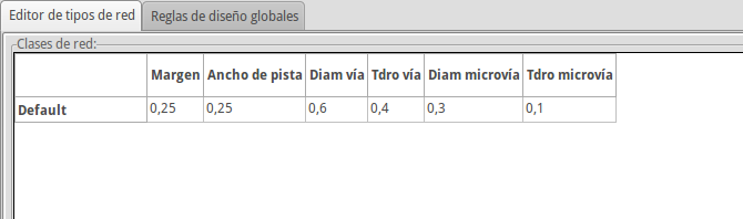
-
Click on the 'Global Design Rules' tab and set 'Minimum track width' to '0.25'. Click the OK button to commit your changes and close the Design Rules Editor window.
-
Now we will import the netlist file if you created one. Click on the 'Read netlist' icon
on the top toolbar. The netlist file 'tutorial1.net' should be selected in the 'Netlist file' field if it was created from Eeschema. Click on 'Read Current Netlist'. Then click the 'Close' button. -
All components should now be visible. They are selected and follow the mouse cursor.
-
Move the components to the middle of the board. If necessary you can zoom in and out while you move the components. Click the left mouse button.
-
All components are connected via a thin group of wires called ratsnest. Make sure that the 'Show/hide board ratsnest' button
 is pressed. In this way you can see the ratsnest linking all components.
 -
You can move each component by hovering over it and pressing [m]. Click where you want to place them. Alternatively you can select a component by clicking on it and then drag it. Press [r] to rotate a component. Move all components around until you minimise the number of wire crossovers.
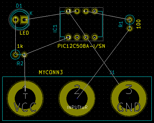
-
Note how one pin of the 100 ohm resistor is connected to pin 6 of the PIC component. This is the result of the labelling method used to connect pins. Labels are often preferred to actual wires because they make the schematic much less messy.
-
Now we will define the edge of the PCB. Select the 'Edge.Cuts' layer from the drop-down menu in the top toolbar. Click on the 'Add graphic lines' icon
 on the right toolbar. Trace around the edge of the board, clicking at each corner, and remember to leave a small gap between the edge of the green and the edge of the PCB.
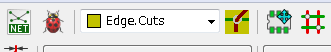
-
A continuación, conecte todos los hilos excepto el de GND. De hecho, vamos a conectar todas las conexiones GND de una sola vez usando un plano de tierra situado en capa de cobre de la parte inferior de la placa (llamada B.Cu).
-
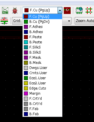
Ahora tenemos que elegir sobre qué capa de cobre que queremos trabajar. Seleccione 'F.Cu (PgUp)' en el menú desplegable de la barra de herramientas superior. Esta es la capa de cobre superior.
-
If you decide, for instance, to do a 4 layer PCB instead, go to Setup → Layers Setup and change 'Copper Layers' to 4. In the 'Layers' table you can name layers and decide what they can be used for. Notice that there are very useful presets that can be selected via the 'Preset Layer Groupings' menu.
-
Click on the 'Route tracks' icon
 on the right toolbar. Click on pin 1 of 'J1' and run a track to pad 'R2'. Double-click to set the point where the track will end. The width of this track will be the default 0.250 mm. You can change the track width from the drop-down menu in the top toolbar. Mind that by default you have only one track width available.
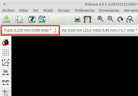
-
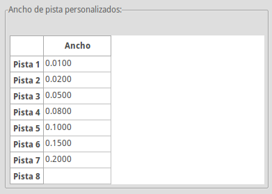
If you would like to add more track widths go to: Setup → Design Rules → Global Design Rules tab and at the bottom right of this window add any other width you would like to have available. You can then choose the widths of the track from the drop-down menu while you lay out your board. See the example below (inches).
-
Alternatively, you can add a Net Class in which you specify a set of options. Go to Setup → Design Rules → Net Classes Editor and add a new class called 'power'. Change the track width from 8 mil (indicated as 0.0080) to 24 mil (indicated as 0.0240). Next, add everything but ground to the 'power' class (select 'default' at left and 'power' at right and use the arrows).
-
If you want to change the grid size, Right click → Grid. Be sure to select the appropriate grid size before or after laying down the components and connecting them together with tracks.
-
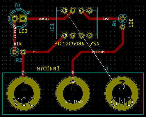
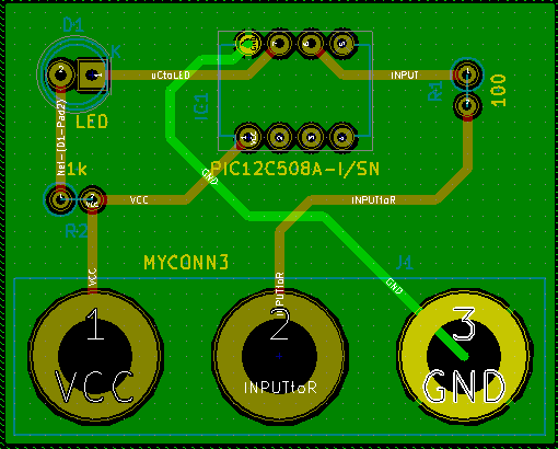
Repita este proceso hasta que todos los cables, excepto el pin 3 de J1, están conectados. Su placa debe ser similar al siguiente ejemplo.
-
Let’s now run a track on the other copper side of the PCB. Select 'B.Cu' in the drop-down menu on the top toolbar. Click on the 'Route tracks' icon
. Draw a track between pin 3 of J1 and pin 8 of U1. This is actually not necessary since we could do this with the ground plane. Notice how the colour of the track has changed. -
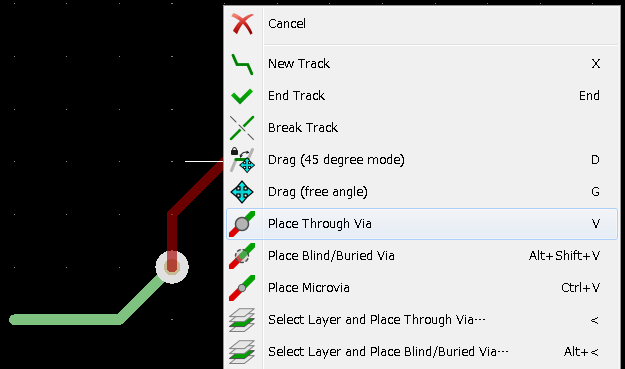
Go from pin A to pin B by changing layer. It is possible to change the copper plane while you are running a track by placing a via. While you are running a track on the upper copper plane, right click and select 'Place Via' or simply press [v]. This will take you to the bottom layer where you can complete your track.
-
When you want to inspect a particular connection you can click on the 'Highlight net' icon
 on the right toolbar. Click on pin 3 of J1. The track itself and all pads connected to it should become highlighted.
 -
Now we will make a ground plane that will be connected to all GND pins. Click on the 'Add filled zones' icon
 on the right toolbar. We are going to trace a rectangle around the board, so click where you want one of the corners to be. In the dialogue that appears, set 'Default pad connection' to 'Thermal relief' and 'Outline slope' to 'H,V and 45 deg only' and click OK.
 -
Trace around the outline of the board by clicking each corner in rotation. Finish your rectangle by clicking the first corner second time. Right click inside the area you have just traced. Click on 'Zones'→'Fill or Refill All Zones'. The board should fill in with green and look something like this:
-
Run the design rules checker by clicking on the 'Perform design rules check' icon
 on the top toolbar. Click on 'Start DRC'. There should be no errors. Click on 'List Unconnected'. There should be no unconnected items. Click OK to close the DRC Control dialogue.
 -
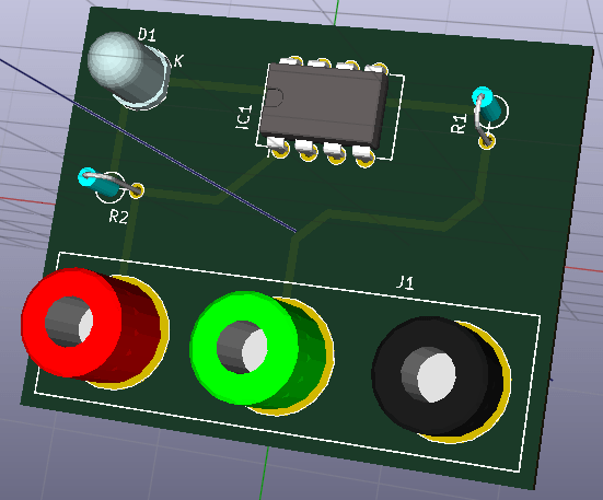
Guarde el archivo haciendo clic en Archivo → Guardar. Para contemplar su placa en 3D, haga clic en Vista → Visor 3D.
-
Puede arrastrar el ratón para rotar la PCB.
-
Su placa está finalizada. Para enviarla a un fabricante tendrá que generar todos los archivos Gerber.
Generar archivos Gerber
Una finalizada la PCB, puede generar archivos Gerber para cada capa y enviarlos a su fabricante de PCB favorito, quien fabricará la placa para usted.
-
From KiCad, open the Pcbnew board editor.
-
Click on File → Plot. Select 'Gerber' as the 'Plot format' and select the folder in which to put all Gerber files. Proceed by clicking on the 'Plot' button.
-
Para generar el archivo de taladrado, desde Pcbnew vaya de nuevo a Archivo → Trazar. Los ajustes por defecto deberían estar bien.
-
Estas son las capas que necesita para seleccionar para realizar una PCB de 2 capas típica:
| Layer | KiCad Layer Name | Default Gerber Extension | "Use Protel filename extensions" is enabled |
|---|---|---|---|
Bottom Layer |
B.Cu |
.GBR |
.GBL |
Top Layer |
F.Cu |
.GBR |
.GTL |
Top Overlay |
F.SilkS |
.GBR |
.GTO |
Bottom Solder Resist |
B.Mask |
.GBR |
.GBS |
Top Solder Resist |
F.Mask |
.GBR |
.GTS |
Edges |
Edge.Cuts |
.GBR |
.GM1 |
Usando GerbView
-
To view all your Gerber files go to the KiCad project manager and click on the 'GerbView' icon. On the drop-down menu or in the Layers manager select 'Graphic layer 1'. Click on File → Open Gerber file(s) or click on the icon
 . Select and open all generated Gerber files. Note how they all get displayed one on top of the other.
 -
Open the drill files with File → Open Excellon Drill File(s).
-
Use the Layers manager on the right to select/deselect which layer to show. Carefully inspect each layer before sending them for production.
-
The view works similarly to Pcbnew. Right click inside the view and click 'Grid' to change the grid.
Trazado automático con FreeRouter
Routing a board by hand is quick and fun, however, for a board with lots of components you might want to use an autorouter. Remember that you should first route critical traces by hand and then set the autorouter to do the boring bits. Its work will only account for the unrouted traces. The autorouter we will use here is FreeRouting.
| FreeRouting is an open source java application. Currently FreeRouting exists in several more or less identical copies which you can find by doing an internet search for "freerouting". It may be found in source only form or as a precompiled java package. |
-
From Pcbnew click on File → Export → Specctra DSN and save the file locally. Launch FreeRouter and click on the 'Open Your Own Design' button, browse for the dsn file and load it.
-
FreeRouter tiene algunas características que KiCad actualmente no tiene, tanto para el trazado manual como para el trazado automático. FreeRouter opera en dos pasos: en primer lugar, traza la placa y luego la optimiza. Una optimización completa puede tardar mucho tiempo, sin embargo se puede detener en cualquier momento cuando lo considere necesario.
-
Puede iniciar el trazado automático haciendo clic en el botón 'Autoruter' en la barra superior. La barra inferior le da información sobre el proceso de trazado en curso. Si el recuento del 'Pass' se pone por encima de 30, tu tabla, probablemente no se puede trazar automáticamente con este router. Separe sus componentes más o gírelos mejor y vuelva a intentarlo. El objetivo de la rotación y la posición de las partes es reducir el número de líneas cruzadas en el ratsnest.
-
Haciendo clic izquierdo con el ratón puede detener el trazado automático e iniciar automáticamente el proceso de optimización. Otro clic izquierdo detendrá el proceso de optimización. A menos que usted realmente necesite detenerlo, es mejor dejar que FreeRouter termine su trabajo.
-
Haga clic en el menú File → Export Specctra Session File y guarde el archivo de placa con la extensión .ses. No necesita guardar el archivo de reglas FreeRouter.
-
Back to Pcbnew. You can import your freshly routed board by clicking on File → Import → Spectra Session and selecting your .ses file.
If there is any routed trace that you do not like, you can delete it and re-route it again, using [Delete] and the routing tool, which is the 'Route tracks' icon ![]() on the right toolbar.
on the right toolbar.
Anotado hacia adelante en KiCad
Una vez que haya completado su esquema electrónico, la asignación de huellas, el diseño de la placa y generado los archivos Gerber, está listo para enviar todo a un fabricante de PCB para que su placa pueda convertirse en realidad.
A menudo, este flujo de trabajo lineal resulta no ser tan unidireccional. Por ejemplo, cuando se tiene que modificar/ampliar una placa que ya haya completado este flujo de trabajo, es posible que necesite mover los componentes alrededor, sustituirlos por otros, cambiar huellas o mucho más. Durante este proceso de modificación, lo que no quiere hacer es modificar de nuevo el trazado de toda la placa desde cero. En su lugar, se realiza del siguiente modo:
-
Supongamos que desea reemplazar el conector CON1 por CON2.
-
Ya tiene un esquema completo y un PCB totalmente trazada.
-
Desde KiCad, inicie Eeschema, haga sus modificaciones suprimiendo CON1 y añadiendo CON2. Guarde su proyecto de esquema mediante el icono
 y haga clic en el icono 'Generar Netlist' en la barra de herramientas superior.
 -
Haga clic en 'Netlist' y después en 'guardar'. Guarde con el nombre de archivo predeterminado. Tiene que volver a escribir el antiguo.
-
Ahora asigne una huella a CON2. Haga clic en el icono 'Run cvpcb'
en la barra de herramientas superior. Asigne la huella al nuevo dispositivo CON2. El resto de los componentes todavía tienen las huellas previamente asignadas. Cerrar Cvpcb. -
De vuelta en el editor de esquemas, guarde el proyecto, haga clic en 'Archivo' → 'Guardar todo el Proyecto de esquema'. Cierre el editor de esquemas.
-
Desde el gestor del proyecto de KiCad, haga clic en el icono 'Pcbnew'. La ventana 'Pcbnew' se abrirá.
-
La vieja placa, ya trazada, se abre automáticamente. Vamos a importar el nuevo archivo netlist. Haga clic en el icono 'Leer Netlist'
en la barra de herramientas superior. -
Haga clic en el botón "Examinar Archivos Netlist", seleccione el archivo netlist en la ventana de selección de archivos y haga clic en 'Leer Netlist actual'. Luego haga clic en el botón "Cerrar".
-
En este punto, debería poder ver un diseño con todos los componentes anteriores ya conectados. En la esquina superior izquierda debería ver todos los componentes no conectados, en nuestro caso CON2. Seleccione CON2 con el ratón. Mueva el componente al centro de la placa.
-
Coloque CON2 y trace sus conexiones. Una vez hecho esto, guarde y continúe con la generación de archivos Gerber, como de costumbre.
El proceso descrito aquí puede ser fácilmente repetir tantas veces como sea necesario. Junto a la técnica de la anotación hacia adelante descrita anteriormente, hay otro método conocido como Anotación hacia atrás. Este método le permite hacer modificaciones a su PCB ya trazada desde Pcbnew y actualizar esas modificaciones en el archivo de esquema y archivo netlist. El método de anotación hacia atrás, sin embargo, no es tan útil y por lo tanto no se describe aquí.
Make schematic symbols in KiCad
Sometimes a symbol that you want to place on your schematic is not in a KiCad library. This is quite normal and there is no reason to worry. In this section we will see how a new schematic symbol can be quickly created with KiCad. Nevertheless, remember that you can always find KiCad components on the Internet.
In KiCad, a symbol is a piece of text that starts with 'DEF' and ends with 'ENDDEF'. One or more symbols are normally placed in a library file with the extension .lib. If you want to add symbols to a library file you can just use the cut and paste commands of a text editor.
Usando el editor de bibliotecas de componentes
-
Podemos utilizar el Editor de Bibliotecas de Componentes _ (parte de Eeschema) para hacer nuevos componentes. En el directorio de nuestro proyecto 'Tutorial1' vamos a crear una carpeta llamada "biblioteca". Dentro pondremos nuestro nuevo archivo de biblioteca _myLib.lib tan pronto como hayamos creado nuestro nuevo componente.
-
Now we can start creating our new component. From KiCad, start Eeschema, click on the 'Library Editor' icon
 and then click on the 'New component' icon
  . The Component Properties window will appear. Name the new component 'MYCONN3', set the 'Default reference designator' as 'J', and the 'Number of units per package' as '1'. Click OK. If the warning appears just click yes. At this point the component is only made of its labels. Let’s add some pins. Click on the 'Add Pins' icon
  on the right toolbar. To place the pin, left click in the centre of the part editor sheet just below the 'MYCONN3' label.
 -
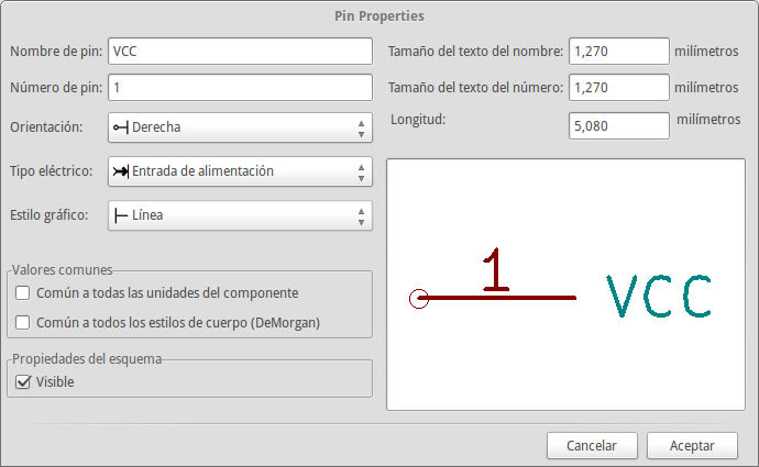
In the Pin Properties window that appears, set the pin name to 'VCC', set the pin number to '1', and the 'Electrical type' to 'Power input' then click OK.
-
Coloque el pin haciendo clic en el lugar donde desee situarlo, justo debajo de la etiqueta 'MYCONN3'.
-
Repita los pasos utilizando esta vez el 'nombre de Pin' 'INPUT', 'número Pin' debe ser '2', y 'Tipo Electrico' a 'Pasivo'.
-
Repita de nuevo los pasos, cree esta vez un Pin con 'nombre' 'GND', 'número Pin' igual a '3' y 'Tipo Electrico' como 'Pasivo'. Coloque los pines uno encima del otro. La etiqueta del componente 'MYCONN3' debe estar en el centro de la página (donde las líneas azules se cruzan).
-
A continuación, dibuje el contorno del componente. Haga clic en el icono 'Añadir rectángulo'
 . Queremos dibujar un rectángulo junto a los pines, como se muestra a continuación. Para ello, haga clic donde desee situar la esquina superior izquierda del rectángulo (no mantenga pulsado el botón del ratón). Haga clic de nuevo para ubicar la esquina inferior derecha del rectángulo.
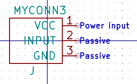
-
If you want to fill the rectangle with yellow, set the fill colour to 'yellow 4' in Preferences → Select color scheme, then select the rectangle in the editing screen with [e], selecting 'Fill background'.
-
Guarde el componente en su biblioteca myLib.lib . Haga clic en el icono 'Nueva Biblioteca' image:images/icons/new_library.png[new_library_png, navegue hasta el directorio tutorial1/biblioteca/ y guarde el nuevo archivo de biblioteca con el nombre myLib.lib.
-
Vaya a Preferencias → Bibliotecas de componentes y añada tutorial1/biblioteca/ en 'ruta de búsqueda definida por el usuario' y myLib.lib en 'archivos de la biblioteca de componentes'.
-
Haga clic en el icono 'Seleccionar biblioteca de trabajo'
 . En la ventana de selección de biblioteca haga clic en myLib y haga clic en Aceptar. Observe cómo la cabecera de la ventana indica la biblioteca actualmente en uso, que ahora debe ser myLib.
 -
Haga clic en el icono "Actualizar componente actual en biblioteca actual'
 en la barra de herramientas superior. Guarde todos los cambios haciendo clic en el icono 'Guardar biblioteca actual en disco'
  en la barra de herramientas superior. Haga clic en "Sí" en los mensajes de confirmación que aparecen. El nuevo símbolo de componente se ha creado y está disponible en la biblioteca indicada en la barra de título de la ventana.
 -
Ahora puede cerrar la ventana del editor de la biblioteca de componentes. Volverá a la ventana del editor de esquema. Su nuevo componente estará disponible en la biblioteca myLib.
-
Puede hacer cualquier archivo de biblioteca file.lib disponible añadiéndolo a la ruta de bibliotecas. Desde Eeschema, vaya a Preferencias → * Biblioteca * y añadir la ruta de acceso a la misma en la 'ruta definida por el usuario de búsqueda "y file.lib en' archivos de la biblioteca de componentes".
Exportar, importar y modificar componentes de la biblioteca
En lugar de crear un componente de biblioteca desde cero a veces es más fácil empezar desde uno ya hecho y modificarlo. En esta sección veremos cómo exportar un componente de la biblioteca "device" estándar de KiCad a su propia biblioteca myOwnLib.lib y luego modificarlo.
-
Desde KiCad, inicie Eeschema, haga clic en el icono 'Editor de Bibliotecas'
, haga clic en el icono 'Seleccionar biblioteca de trabajo' y elija la biblioteca 'device'. Haga clic en el icono 'cargar componente a editar desde la biblioteca actual'  e importe el componente 'RELAY_2RT'.
 -
Haga clic en el icono 'Exportar componente'
 , navegue dentro del directorio library/ y guarde el nuevo archivo de biblioteca con el nombre myOwnLib.lib.
 -
You can make this component and the whole library myOwnLib.lib available to you by adding it to the library path. From Eeschema, go to Preferences → Component Libraries and add both library/ in 'User defined search path' and myOwnLib.lib in the 'Component library files'. Close the window.
-
Haga clic en el icono 'Seleccionar biblioteca de trabajo '
. En la ventana de Selección de Bibliotecas haga clic en myOwnLib y haga clic en Aceptar. Observe cómo el titulo de la ventana indica la biblioteca actualmente en uso, debe ser myOwnLib. -
Haga clic en el icono de "Cargar componente a editar de la biblioteca actual'
e importe el componente 'RELAY_2RT'. -
You can now modify the component as you like. Hover over the label 'RELAY_2RT', press [e] and rename it 'MY_RELAY_2RT'.
-
Haga clic en el icono 'Actualizar componente en biblioteca actual'
en la barra de herramientas superior. Guarde todos los cambios haciendo clic en el icono 'Guardar biblioteca actual en disco' en la barra de herramientas superior.
Hacer símbolos de componentes con quicklib
En esta sección se presenta un método alternativo para crear el símbolo del componente MYCONN3 (ver MYCONN3 arriba) utilizando la herramienta de Internet quicklib.
-
Vaya a la página web de quicklib: http://kicad.rohrbacher.net/quicklib.php
-
Rellene la página con la siguiente información: Component name: MYCONN3, Reference Prefix: J, Pin Layout Style: SIL, Pin Count, N: 3
-
Haga clic en el icono 'Asignar Pines'. Rellene la página con la siguiente información: Pin 1: VCC, Pin 2: INPUT, Pin 3: GND. Tipo: Pasivo para los 3 pines.
-
Haga clic en el icono de 'vista previa' y, si está satisfecho, haga clic en el 'Construir biblioteca de componentes ". Descargue el archivo y cámbiele el nombre por tutorial1/library/myQuickLib.lib.. ¡Ya está listo!
-
Echémosle un vistazo usando KiCad. Desde el gestor del proyecto de KiCad, inicie Eeschema, haga clic en el icono 'Editor de Bibliotecas'
, haga clic en el icono de 'Importar componentes'  , vaya a tutorial1/library/ y seleccione myQuickLib.lib.
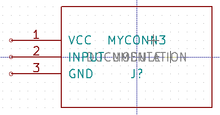
-
Puede disponer de este componente y de toda la biblioteca myQuickLib.lib añadiéndolos a la ruta de bibliotecas de KiCad. Desde Eeschema, vaya a Preferencias → Bibliotecas de componentes y añada library en 'rutas de búsqueda definidas por el usuario' y myQuickLib.lib en 'archivos de la biblioteca de componentes'.
Como puede imaginar, este método de creación de componentes de la biblioteca puede ser muy eficaz cuando se desea crear componentes con un gran número de pines.
Realizar símbolos de componentes con gran número de pines
En la sección titulada Realizar símbolos de componentes en quicklib vimos cómo hacer un símbolo de componente utilizando la herramienta web quicklib. Sin embargo, ocasionalmente puede que necesite crear un símbolo de componente con un alto número de pines (algunos cientos de pines). En KiCad, esto no es muy complicado.
-
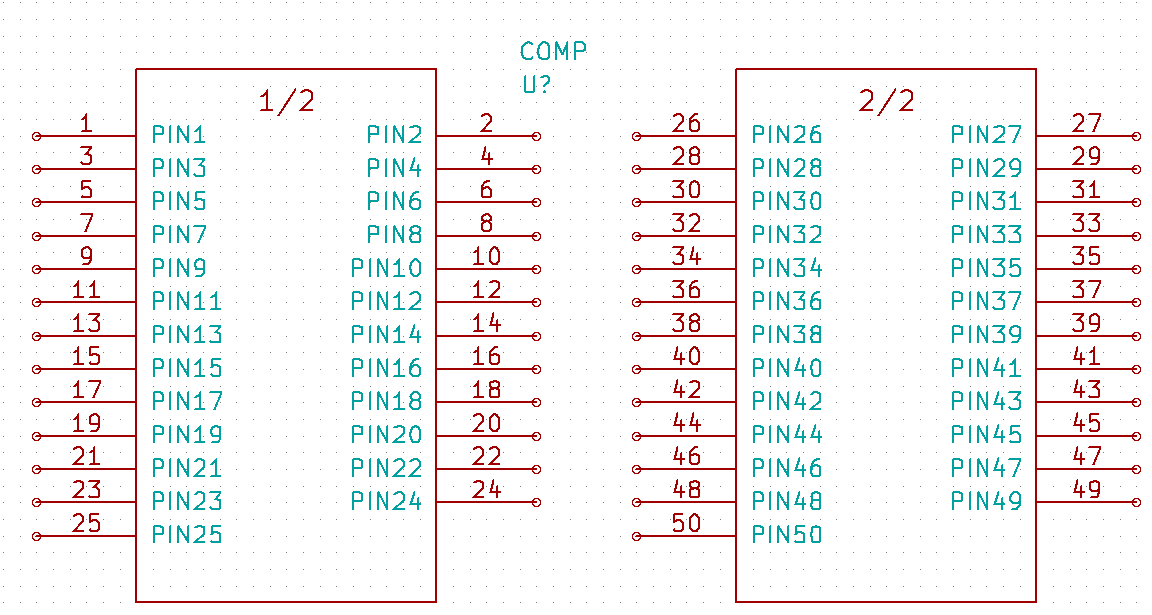
Supongamos que desea crear un símbolo de un dispositivo con 50 pines. Es una práctica común dibujarlo usando varios símbolos de bajo número de pines, por ejemplo dos símbolos con 25 pines cada uno. Esta representación permite una fácil conexión de los pines.
-
La mejor manera de crear nuestro componente es utilizar quicklib para generar dos componentes de 25 pines por separado, re-numerar sus pines utilizando un script de Python y finalmente fusionar los dos mediante el uso de copiar y pegar para convertirlos en un solo componente dentro de la estructura DEF y ENDDEF.
-
A continuación se muestra un ejemplo de un script de Python sencillo que se puede utilizar en combinación con un archivo in.txt y un archivo out.txt para re-numerar la línea: X PIN1 1 -750 600 300 R 50 50 1 1 I en X PIN26 26 -750 600 300 R 50 50 1 1 I esto se hace para todas las líneas en el archivo in.txt.
Script
#!/usr/bin/env python
''' simple script to manipulate KiCad component pins numbering'''
import sys, re
try:
    fin=open(sys.argv[1],'r')
    fout=open(sys.argv[2],'w')
except:
    print "oh, wrong use of this app, try:", sys.argv[0], "in.txt out.txt"
    sys.exit()
for ln in fin.readlines():
    obj=re.search("(X PIN)(\d*)(\s)(\d*)(\s.*)",ln)
if obj:
    num = int(obj.group(2))+25
    ln=obj.group(1) + str(num) + obj.group(3) + str(num) + obj.group(5) +'\n'
    fout.write(ln)
fin.close(); fout.close()
#
# for more info about regular expression syntax and KiCad component generation:
# http://gskinner.com/RegExr/
# http://kicad.rohrbacher.net/quicklib.php-
Mientras fusiona los dos componentes en uno solo, es necesario utilizar el Editor de bibliotecas de Eeschema para mover el primer componente de modo que el segundo no se ubique sobre este. A continuación encontrará el archivo .lib final y su representación en Eeschema.
Contenido del fichero *.lib
EESchema-LIBRARY Version 2.3
#encoding utf-8
# COMP
DEF COMP U 0 40 Y Y 1 F N
F0 "U" -1800 -100 50 H V C CNN
F1 "COMP" -1800 100 50 H V C CNN
DRAW
S -2250 -800 -1350 800 0 0 0 N
S -450 -800 450 800 0 0 0 N
X PIN1 1 -2550 600 300 R 50 50 1 1 I

...

X PIN49 49 750 -500 300 L 50 50 1 1 I
ENDDRAW
ENDDEF
#End Library
-
El script de Python mostrado es una herramienta muy potente para manipular tanto el número del pin como su etiquetas. Tenga en cuenta, sin embargo, que todo su poder viene de la sintaxis de expresiones regulares primitiva y sin embargo increíblemente útil: http: //gskinner.com/RegExr/.
Realizar huellas de componentes
Unlike other EDA software tools, which have one type of library that contains both the schematic symbol and the footprint variations, KiCad .lib files contain schematic symbols and .kicad_mod files contain footprints. Cvpcb is used to map footprints to symbols.
Igual que los archivos .lib, los archivos de biblioteca .kicad_mod son archivos de texto plano que pueden contener cualquier cosa, desde una a varias partes.
Hay una extensa librería de componentes en KiCad, sin embargo, en ocasiones puede encontrarse con que la huella que necesita no está en la biblioteca. Estos son los pasos para crear una nueva huella para PCB en KiCad:
Usando el editor de huellas
-
Desde el gestor del proyecto en KiCad inicie la herramienta Pcbnew. Haga clic en el icono 'Abrir Editor de huellas' images/icons/edit_module.png[edit_module_png] en la barra de herramientas superior. Esto abrirá el 'Editor de Huellas'.
-
We are going to save the new footprint 'MYCONN3' in the new footprint library 'myfootprint'. Create a new folder myfootprint.pretty in the tutorial1/ project folder. Click on the Preferences → Footprint Libraries Manager and press 'Append Library' button. In the table, enter "myfootprint" as Nickname, enter "${KIPRJMOD}/myfootprint.pretty" as Library Path and enter "KiCad" as Plugin Type. Press OK to close the PCB Library Tables window. Click on the 'Select active library' icon
 on the top toolbar. Select the 'myfootprint' library.
 -
Haga clic en el icono de 'Nueva Huella'
 en la barra de herramientas superior. Escriba 'MYCONN3' como 'nombre de huella'. En el centro de la pantalla aparecerá la etiqueta 'MYCONN3'. Bajo esta etiqueta se puede ver la etiqueta 'REF*'. Haga clic derecho sobre 'MYCONN3' y muévalo por encima de 'REF*'. Haga clic derecho sobre 'REF*__', seleccione 'Editar texto' y cambie su nombre por 'SMD'. Establezca el valor de 'Display' a 'invisible'.
 -
Select the 'Add Pads' icon
 on the right toolbar. Click on the working sheet to place the pad. Right click on the new pad and click 'Edit Pad'. You can also use [e].
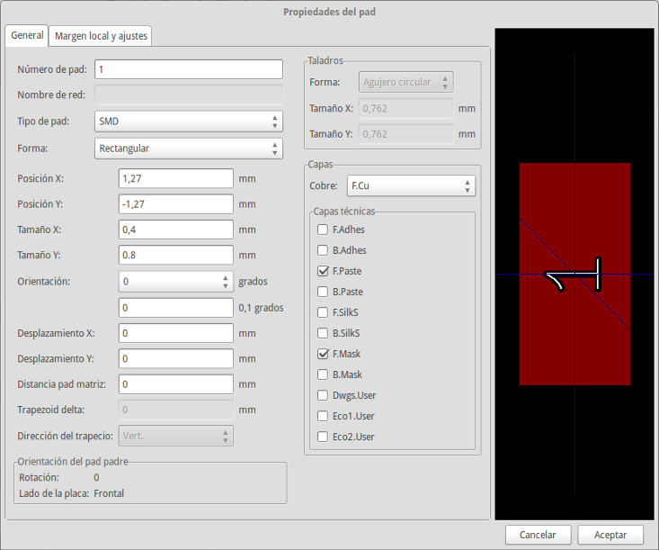
-
Ajuste el 'Número de Pad' a '1', 'Forma del Pad' a 'Rect', 'Tipo de Pad' a 'SMD', 'Tamaño X' a '0.4' y 'Tamaño Y' a '0.8'. Haga clic en Aceptar. Haga clic de nuevo en 'Añadir Pads' y coloque dos pads más.
-
Si desea cambiar el tamaño de la rejilla, Clic derecho → Selección de Rejilla. Asegúrese de seleccionar el tamaño de la rejilla adecuado antes de que se situar los componentes.
-
Mueva la etiquetas 'MYCONN3' y 'SMD' aparte para que se vea como la imagen se mostrada arriba.
-
Al colocar los pads a menudo es necesario medir distancias relativas. Coloque el cursor donde desee situar el punto de coordenada relativa (0,0) y pulse la barra espaciadora. Mientras se mueve el cursor, verá una indicación relativa de la posición del cursor en la parte inferior de la página. Pulse la barra espaciadora en cualquier momento para establecer el nuevo origen.
-
Ahora agregue un contorno para huella. Haga clic en el icono 'Añadir línea gráfica o polígono'
 en la barra de herramientas derecha. Dibuje un esquema del conector alrededor del componente.
 -
Haga clic en el icono 'Guardar Huella en Biblioteca Activa'
en la barra de herramientas superior, utilizando el nombre predeterminado MYCONN3.
Notas sobre portabilidad de los proyectos en KiCad
¿Qué archivos necesita enviar a alguien para que pueda cargar totalmente y utilizar su proyecto en KiCad?
Cuando quiere compartir un proyecto de KiCad con alguien, es importante que el archivo de esquema .Sch, el archivo de diseño de placa .Kicad_pcb, el archivo de proyecto .pro y el archivo netlist .Net, sean enviados junto con el fichero biblioteca de símbolos .lib y el archivo de biblioteca de huellas .kicad_mod. Sólo así la gente tendrá total libertad para modificar el esquema y la placa.
Junto con los esquemas de KiCad, la gente necesitará los archivos .lib que contienen los símbolos. Esos archivos de biblioteca necesitan ser cargados en las preferencias de Eeschema. Por otro lado, con las placas (Archivos .kicad_pcb), las huellas pueden ser almacenados dentro del archivo .kicad_pcb. Puede enviar a alguien un archivo .kicad_pcb y nada más, y todavía sería capaz de ver y editar la placa. Sin embargo, cuando quiera cargar los componentes desde un fichero netlist, las bibliotecas de componentes (.Archivos kicad_mod) tendrán que estar presentes y cargadas en las preferencias de Pcbnew al igual que para los esquemas. Además, es necesario cargar los archivos .kicad_mod en las preferencias de Pcbnew para que esas huellas aparezcan en Cvpcb.
Si alguien le envía un archivo .kicad_pcb con huellas que le gustaría utilizar en la otra placa, puede abrir el Editor de Huellas, cargar una huella de la placa actual, y guardar o exportar en otra biblioteca de componentes. También puede exportar todas las huellas de un archivo .kicad_pcb a la vez a través de Pcbnew → Archivo → Archivar → Huellas → Crear archivo huella, que creará un nuevo archivo .kicad_mod con todas las huellas de la placa.
En otras palabras, si lo único que desea distribuir es la PCB, entonces el fichero .kicad_pcb con la placa es suficiente. Sin embargo, si desea dar a la gente la capacidad completa para usar y modificar su esquema, sus componentes y la PCB, es muy recomendable que usted genere un zip y envíe el siguiente directorio del proyecto:
tutorial1/
|-- tutorial1.pro
|-- tutorial1.sch
|-- tutorial1.kicad_pcb
|-- tutorial1.net
|-- library/
|   |-- myLib.lib
|   |-- myOwnLib.lib
|   \-- myQuickLib.lib
|
|-- myfootprint.pretty/
|   \-- MYCONN3.kicad_mod
|
\-- gerber/
    |-- ...
    \-- ...
Mas sobre la documentación de KiCad
Esta es una guía rápida sobre la mayoría de las características de KiCad. Para obtener instrucciones más detalladas consulte los archivos de ayuda accesibles a través de cada módulo de KiCad. Haga clic en Ayuda → Manual.
KiCad viene con un buen conjunto de manuales en varios idiomas para sus cuatro componentes de software.
La versión en Inglés de todos los manuales KiCad se distribuyen con KiCad.
Además de sus manuales, KiCad se distribuye con este tutorial, que ha sido traducido a otros idiomas. Todas las diferentes versiones de este tutorial se distribuyen de forma gratuita con todas las versiones recientes de KiCad. Este tutorial, así como los manuales, deben empaquetarse con su versión de KiCad en su plataforma determinada.
Por ejemplo, en Linux las ubicaciones típicas son los siguientes directorios, dependiendo de su distribución exacta:
/usr/share/doc/kicad/help/en/
/usr/local/share/doc/kicad/help/en
En Windows se encuentran en:
<directorio de instalación>/share/doc/kicad/help/en
En OS X:
/Library/Application Support/kicad/help/en
Documentación de KiCad en la Web
The latest version of KiCad documentation can be found in multiple languages at http://docs.kicad.org